EP3709538A1 - On-chip phased array calibration systems and methods - Google Patents
On-chip phased array calibration systems and methods Download PDFInfo
- Publication number
- EP3709538A1 EP3709538A1 EP20160945.0A EP20160945A EP3709538A1 EP 3709538 A1 EP3709538 A1 EP 3709538A1 EP 20160945 A EP20160945 A EP 20160945A EP 3709538 A1 EP3709538 A1 EP 3709538A1
- Authority
- EP
- European Patent Office
- Prior art keywords
- channel
- channels
- phase
- gain
- memory
- Prior art date
- Legal status (The legal status is an assumption and is not a legal conclusion. Google has not performed a legal analysis and makes no representation as to the accuracy of the status listed.)
- Granted
Links
Images



Classifications
-
- H—ELECTRICITY
- H04—ELECTRIC COMMUNICATION TECHNIQUE
- H04B—TRANSMISSION
- H04B17/00—Monitoring; Testing
- H04B17/20—Monitoring; Testing of receivers
- H04B17/21—Monitoring; Testing of receivers for calibration; for correcting measurements
- H04B17/22—Monitoring; Testing of receivers for calibration; for correcting measurements for calibration of the receiver components
- H04B17/221—Monitoring; Testing of receivers for calibration; for correcting measurements for calibration of the receiver components of receiver antennas, e.g. as to amplitude or phase
-
- G—PHYSICS
- G01—MEASURING; TESTING
- G01S—RADIO DIRECTION-FINDING; RADIO NAVIGATION; DETERMINING DISTANCE OR VELOCITY BY USE OF RADIO WAVES; LOCATING OR PRESENCE-DETECTING BY USE OF THE REFLECTION OR RERADIATION OF RADIO WAVES; ANALOGOUS ARRANGEMENTS USING OTHER WAVES
- G01S7/00—Details of systems according to groups G01S13/00, G01S15/00, G01S17/00
- G01S7/02—Details of systems according to groups G01S13/00, G01S15/00, G01S17/00 of systems according to group G01S13/00
- G01S7/40—Means for monitoring or calibrating
- G01S7/4004—Means for monitoring or calibrating of parts of a radar system
-
- H—ELECTRICITY
- H01—ELECTRIC ELEMENTS
- H01Q—ANTENNAS, i.e. RADIO AERIALS
- H01Q21/00—Antenna arrays or systems
- H01Q21/06—Arrays of individually energised antenna units similarly polarised and spaced apart
- H01Q21/22—Antenna units of the array energised non-uniformly in amplitude or phase, e.g. tapered array or binomial array
-
- H—ELECTRICITY
- H01—ELECTRIC ELEMENTS
- H01Q—ANTENNAS, i.e. RADIO AERIALS
- H01Q3/00—Arrangements for changing or varying the orientation or the shape of the directional pattern of the waves radiated from an antenna or antenna system
- H01Q3/26—Arrangements for changing or varying the orientation or the shape of the directional pattern of the waves radiated from an antenna or antenna system varying the relative phase or relative amplitude of energisation between two or more active radiating elements; varying the distribution of energy across a radiating aperture
- H01Q3/267—Phased-array testing or checking devices
-
- H—ELECTRICITY
- H01—ELECTRIC ELEMENTS
- H01Q—ANTENNAS, i.e. RADIO AERIALS
- H01Q3/00—Arrangements for changing or varying the orientation or the shape of the directional pattern of the waves radiated from an antenna or antenna system
- H01Q3/26—Arrangements for changing or varying the orientation or the shape of the directional pattern of the waves radiated from an antenna or antenna system varying the relative phase or relative amplitude of energisation between two or more active radiating elements; varying the distribution of energy across a radiating aperture
- H01Q3/28—Arrangements for changing or varying the orientation or the shape of the directional pattern of the waves radiated from an antenna or antenna system varying the relative phase or relative amplitude of energisation between two or more active radiating elements; varying the distribution of energy across a radiating aperture varying the amplitude
-
- H—ELECTRICITY
- H01—ELECTRIC ELEMENTS
- H01Q—ANTENNAS, i.e. RADIO AERIALS
- H01Q3/00—Arrangements for changing or varying the orientation or the shape of the directional pattern of the waves radiated from an antenna or antenna system
- H01Q3/26—Arrangements for changing or varying the orientation or the shape of the directional pattern of the waves radiated from an antenna or antenna system varying the relative phase or relative amplitude of energisation between two or more active radiating elements; varying the distribution of energy across a radiating aperture
- H01Q3/30—Arrangements for changing or varying the orientation or the shape of the directional pattern of the waves radiated from an antenna or antenna system varying the relative phase or relative amplitude of energisation between two or more active radiating elements; varying the distribution of energy across a radiating aperture varying the relative phase between the radiating elements of an array
-
- H—ELECTRICITY
- H04—ELECTRIC COMMUNICATION TECHNIQUE
- H04B—TRANSMISSION
- H04B17/00—Monitoring; Testing
- H04B17/10—Monitoring; Testing of transmitters
- H04B17/11—Monitoring; Testing of transmitters for calibration
- H04B17/13—Monitoring; Testing of transmitters for calibration of power amplifiers, e.g. gain or non-linearity
-
- H—ELECTRICITY
- H04—ELECTRIC COMMUNICATION TECHNIQUE
- H04B—TRANSMISSION
- H04B7/00—Radio transmission systems, i.e. using radiation field
- H04B7/02—Diversity systems; Multi-antenna system, i.e. transmission or reception using multiple antennas
- H04B7/04—Diversity systems; Multi-antenna system, i.e. transmission or reception using multiple antennas using two or more spaced independent antennas
- H04B7/06—Diversity systems; Multi-antenna system, i.e. transmission or reception using multiple antennas using two or more spaced independent antennas at the transmitting station
- H04B7/0613—Diversity systems; Multi-antenna system, i.e. transmission or reception using multiple antennas using two or more spaced independent antennas at the transmitting station using simultaneous transmission
- H04B7/0615—Diversity systems; Multi-antenna system, i.e. transmission or reception using multiple antennas using two or more spaced independent antennas at the transmitting station using simultaneous transmission of weighted versions of same signal
- H04B7/0617—Diversity systems; Multi-antenna system, i.e. transmission or reception using multiple antennas using two or more spaced independent antennas at the transmitting station using simultaneous transmission of weighted versions of same signal for beam forming
Definitions
- the present disclosure relates to an antenna array, in particular to calibration of the antenna array.
- Phased antenna arrays generally refer to a collection of antenna elements that may be used to focus electromagnetic energy in a particular direction creating a main beam. Phased antenna arrays are being used more frequently in a myriad of different applications, such as in military applications, mobile technology, on airplane radar technology, automotive radars, cellular telephone and data, and Wi-Fi technology.
- the individual antenna elements of a phased-antenna array may radiate in a spherical pattern, but collectively generate a wavefront in a particular direction through constructive and destructive interference.
- the relative phases of the signal transmitted at each antenna element can be either fixed or adjusted, allowing the antenna system to steer the wavefront in different directions.
- a phased-antenna array typically includes an oscillator, a plurality of antenna elements, a phase adjuster or shifter, a variable gain amplifier, a receiver, and a control processor.
- a phased antenna array system uses phase adjusters or shifters to control the phase of the signal transmitted by an antenna element.
- the radiated patterns of the antenna elements constructively interfere in a particular direction creating a wavefront in that direction, which may sometimes be referred to as the main beam.
- the phased array can realize increased gain and improved signal to noise ratio in the direction of the main beam.
- the radiation pattern may destructively interfere in one or more additional directions other than the direction of the main beam, and can reduce gain in those
- the amplitude of the signals emanating from the antenna elements affects the side lobe levels, where the side lobes are lobes of the radiation pattern that are not in the direction of the main lobe. It is generally preferable to reduce side lobe levels such that the antenna system can focus transmission in a particular desired direction. As such, the precision of the relative phase and amplitude for the elements determine the precision of the beam direction and the side lobe levels, respectively. Thus, the accuracy of the control of the phase shift and amplitude for the collection of antenna elements is important to the implementation of the phased array.
- Some aspects include a controller configured to calibrate a beamforming integrated circuit, the controller comprising: a non-volatile memory configured to store measured gain data for a plurality of channels of a beamforming integrated circuit; and calibration circuitry configured to: determine a reference gain value based at least in part on the measured gain data for the plurality of channels stored at the non-volatile memory; and for each channel of the plurality of channels: determine a difference between a maximum gain value of the channel obtain from the non-volatile memory and the reference gain value; and copy a portion of a variable gain amplifier configuration attenuation table stored in a shared memory of the beamforming integrated circuit to a channel memory associated with the channel, wherein the variable gain amplifier configuration attenuation table comprises configuration settings for variable gain amplifiers of the beamforming integrated circuit, and wherein the portion of the variable gain amplifier configuration attenuation table copied from the shared memory starts at an address corresponding to the difference between the maximum gain value of the channel and the reference gain value.
- At least one channel supports a different maximum gain value than at least one other channel of the plurality of channels.
- each channel of the plurality of channels supports a maximum gain value.
- At least one channel of the plurality of channels supports a different maximum gain value.
- the reference gain value comprises a lowest common value among a set of maximum gain values supported by the plurality of channels, wherein the set of maximum gain values comprises maximum gain values supported by at least one of the plurality of channels.
- the non-volatile memory is further configured to store measured phase data for the plurality of channels
- the calibration circuitry is further configured to: determine a reference phase value based at least in part on the measured phase data for the plurality of channels stored at the non-volatile memory; and for each channel of the plurality of channels: determine a difference between a phase value of the channel obtain from the non-volatile memory and the reference phase value; and copy a portion of a phase shifter configuration table stored in the shared memory of the beamforming integrated circuit to the channel memory associated with the channel, wherein the phase shifter configuration table comprises configuration settings for phase shifters of the beamforming integrated circuit, and wherein the portion of the phase shifter configuration table copied from the shared memory starts at an address corresponding to the difference between the phase value of the channel and the reference phase value.
- the reference gain value is stored in volatile memory.
- the shared memory is a volatile memory.
- the channel memory corresponding to each of the plurality of channels is a volatile memory.
- Some aspects include a method for calibrating a beamforming integrated circuit, the method comprising: storing, in a non-volatile memory, measured gain data for a plurality of channels of a beamforming integrated circuit; and determining, by calibration circuitry, a reference gain value based at least in part on the measured gain data for the plurality of channels stored at the non-volatile memory; and for each channel of the plurality of channels: determining a difference between a maximum gain value of the channel obtain from the non-volatile memory and the reference gain value; and copying a portion of a variable gain amplifier configuration attenuation table stored in a shared memory of the beamforming integrated circuit to a channel memory associated with the channel, wherein the variable gain amplifier configuration attenuation table comprises configuration settings for variable gain amplifiers of the beamforming integrated circuit, and wherein the portion of the variable gain amplifier configuration attenuation table copied from the shared memory starts at an address corresponding to the difference between the maximum gain value of the channel and the reference gain value.
- At least one channel supports a different maximum gain value than at least one other channel of the plurality of channels.
- each channel of the plurality of channels supports a maximum gain value.
- At least one channel of the plurality of channels supports a different maximum gain value.
- the reference gain value comprises a lowest common value among a set of maximum gain values supported by the plurality of channels, wherein the set of maximum gain values comprises maximum gain values supported by at least one of the plurality of channels.
- the method further comprises: storing, in the non-volatile memory, measured phase data for the plurality of channels; determining a reference phase value based at least in part on the measured phase data for the plurality of channels stored at the non-volatile memory; and for each channel of the plurality of channels: determining a difference between a phase value of the channel obtain from the non-volatile memory and the reference phase value; and copying a portion of a phase shifter configuration table stored in the shared memory of the beamforming integrated circuit to the channel memory associated with the channel, wherein the phase shifter configuration table comprises configuration settings for phase shifters of the beamforming integrated circuit, and wherein the portion of the phase shifter configuration table copied from the shared memory starts at an address corresponding to the difference between the phase value of the channel and the reference phase value.
- the reference gain value is stored in volatile memory.
- the shared memory is a volatile memory.
- the channel memory corresponding to each of the plurality of channels is a volatile memory.
- Some aspects include a controller configured to calibrate a beamforming integrated circuit, the controller comprising: calibration circuitry configured to: determine a reference gain value based at least in part on measured gain data for the plurality of channels stored at a non-volatile memory; and for each channel of the plurality of channels: copy a portion of a variable gain amplifier configuration attenuation table stored in a shared memory of the beamforming integrated circuit to a channel memory associated with the channel, wherein the variable gain amplifier configuration attenuation table comprises configuration settings for variable gain amplifiers of the beamforming integrated circuit, and wherein the portion of the variable gain amplifier configuration attenuation table copied from the shared memory starts at an address corresponding to a difference between a maximum gain value of the channel obtain from the non-volatile memory and the reference gain value.
- the reference gain value is stored in volatile memory.
- An antenna array can enable a beamformer to steer or focus an electromagnetic radiation pattern in a particular direction.
- the beamformer may generate a main beam in a particular direction and may generate side lobes in other directions.
- the main beam of the radiation pattern may be generated based on constructive inference of a plurality of signals output by an antenna array.
- the plurality of signals may be aligned by modifying the phases of at least some of the transmitted signal.
- the side-lobe levels may be controlled by adjusting the phases and amplitudes of the signals output by the antenna elements.
- a beamformer can generate a desired antenna pattern by, for example, configuring one or more phase shifter settings and/or one or more variable gain amplifiers to modify the phase and amplitude of signals output by the antenna elements of the beamformer antenna array.
- Systems and methods disclosed herein may be applicable during the manufacturing test process and can be used to speed up production and lower costs. However, techniques disclosed herein may also be applied subsequent to manufacture, such as during incorporation into a device by a third-party or during use of the beamformer.
- the calibration data may be used by the beamformer in combination with other data, such as pre-calculated or pre-stored antenna pattern data, to generate appropriate or desired settings for particular beamforming implementations or use-cases.
- the maximum supported gain and/or the gain range may vary across different channels of the antenna array.
- the phase for each channel may also differ for different channels of the antenna array.
- two channels may communicate at two slightly different angles due to differences between the channels.
- the variance in the gain and/or phase of the different channels may occur due, for example, to variance in fabrication, which may be due to differences or imperfections in manufacturing conditions, manufacturing process, or materials.
- the present disclosure provides systems and methods for calibration of antenna arrays. These antenna arrays may be used in a variety of technologies, such as fifth generation cellular technology (5G), radar, or any other application of phased antenna arrays.
- the present disclosure enables an antenna array system to perform calibration using raw measurements of phase and/or amplitude data.
- the raw measurements of phase and/or amplitude can be stored in a non-volatile memory.
- calibration can be performed, and the performance variance between components on different channels of a transceiver, receiver, or a transmitter can be accounted for during operation of the beamformer based on raw measurements of signals transmitted using the beamformer.
- the raw measurements of gain and/or phase of a channel in the beamformer can be measured by equipment external to the antenna array system and stored in a memory of the beamformer, such as a non-volatile memory, disposed within the antenna array system.
- a memory of the beamformer such as a non-volatile memory, disposed within the antenna array system.
- the antenna array system of the present disclosure does not require substantial hardware modifications for calibration.
- the antenna array system can store the raw measurements of each channel of the antenna array in a non-volatile memory for persistent storage, and the measurements may be retrieved and used for calibration as needed or desired.
- systems and methods of the present disclosure include storing measurements of a maximum supported gain and/or a deviation from a reference phase for channels of a beamforming chip that can be used to control a beamforming chip.
- the beamforming chips may include aspects of beamforming chips described in U.S. Patent Application No. 15/904,045, filed February 23, 2018 , titled “ANTENNA ARRAY CALIBRATION SYSTEMS AND METHODS," and U.S. Patent Application No. 16/178,303, filed November 1, 2018 , titled “LOW-LOSS VECTOR MODULATOR BASED PHASE SHIFTER,” both of which are previously incorporated by reference as stated above.
- the beamforming chip may include or be incorporated as part of the phase array antenna system 10, the receiver 1006 or the transmitter 1008 of U.S. Patent Application No. 16/178,303 .
- the measurements may be stored in a non-volatile memory, and a controller can use the data to calibrate the channels of the beamforming chip.
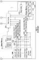
- Figure 1 illustrates an example memory architecture 100 for the beamforming chip according to certain aspects.
- the phase and gain measurements of each of the channels of the beamforming chip can be stored in non-volatile memory (NVM) 104.
- the beamforming chip can identify a reference gain and/or phase 106.
- the reference gain and/or phase 106 can be used to determine a relative variance across the channels of the measured gain and/or phase stored in the non-volatile memory 104.
- the reference gain and reference phase may be stored within the non-volatile memory 104.
- the reference gain and/or phase 106 can be stored in volatile or static memory, such as RAM memory.
- the reference gain and reference phase may be stored within a bypass register or SRAM register of the non-volatile memory.
- the reference gain and reference phase may be stored within a volatile portion of a non-volatile memory system.
- the reference gain and/or phase 106 can be subtracted via a subtractor 108 from the corresponding measurements of gain and/or phase for each of the channels of the beamforming chip can be stored in non-volatile memory 104.
- the subtractor 108 may include or be a substractor.
- the subtractor 108 may include or be replaced by alternative digital logic structures for subtracting the reference gain and/or phase 106 from measurement of gain and/or phase for each of the channels of the beamforming chip.
- the subtractor 108 may include or be replaced with any type of logic that may be generated by a logic design tool, such as an automatic logic generator.
- the reference gain can include a gain measurement of a channel, or be derived from a gain measurement of a channel.
- the reference gain and/or phase 106 can be based on the measurements of gain and/or phase for one or more of the channels of the beamforming chip, and can be stored in non-volatile memory 104.
- the antenna array can include 16 channels, each corresponding to a maximum gain value for the corresponding channel.
- the reference gain can include a lowest common maximum gain value for the channels of the beamforming chip system.
- the reference gain value can be subtracted from the corresponding actual measurements of gain and/or phase for each of the channels of the antenna array and can be stored in non-volatile memory 104.
- the reference gain may be designated as 20 dB as it is the lower maximum among the two channels. It may be desirable to identify the maximum gain that is commonly supported among a set of channels in order to limit a gain of the beamforming chip to a value that can be supported by all channels within the beamformer. For instance, in the previous example it may be undesirable to select a gain of 21 dB because although channel 1 may support such a gain value, channel 0 may not.
- the measurements of maximum gain supported by the channels of the beamforming chip may be obtained during a manufacturing and/or testing process performed with respect to the beamforming chip. It should be understood that each beamforming chip may have different measured maximum gain values due to, for example, variations that may occur during the manufacturing process.
- the reference phase may be selected as an arbitrary angle, for example 0 degrees, 45 degrees, 90 degrees, etc. that can be used to align each of the channels during a calibration process.
- a measurement of the phase of an output signal may be obtained when the input phase of the signal is 0 degrees.
- the channel is set to the desired reference phase of 0 degrees, it may be determined through measurement of the output signal that due, for example, to process variations that the output signal is at 1 degree or 5 degrees. This measurement of phase for each channel may be stored in the NVM 104.
- the measured phase may be subtracted from the selected reference phase (or vice versa) of 0 degrees to obtain an index value for indexing a portion of a phase calibration table stored in a global memory 110.
- This global memory 110 may be shared among channels of the beamforming chip, or in some cases, among multiple beamforming chips.
- the reference phase can include a phase measurement of a channel, or be derived from a phase measurement of a channel.
- the global memory 110 can be used to retrieve calibration data for each of the channels.
- the global memory 110 can be a volatile or static memory.
- the global memory 110 can be used to retrieve gain and/or phase values for each of the channel memory 102.
- the global memory 110 can store a variable gain amplifier configuration table, where the variable gain amplifier configuration table stores configuration settings for variable gain amplifiers of a beamforming integrated circuit.
- the configuration settings can include an attenuation value for the variable gain amplifier for reducing gain from a maximum supported gain to a desired gain.
- the attenuation value stored at an address associated with the common maximum supported gain may be applied to a set of variable gain amplifiers associated with the beamformer channels.
- the maximum supported gain of channel 0 and of the beamformer are the same.
- the attenuation value stored at address 0 of the memory associated with channel 0 is 0 dB.
- the maximum supported gain of channel 1 is 2 dB greater than the common maximum supported gain of the beamformer.
- the attenuation value stored at address 0 of the memory associated with channel 1 is 2 dB.
- the global memory 110 can store a phase shifter configuration table, where the phase shifter configuration table stores configuration settings for phase shifters of a beamforming integrated circuit.
- the configuration settings can include a phase degree for shifting the phase of a signal.
- a portion of the global memory 110 can be copied to corresponding channels of the channel memory 102 as illustrated in Figure 2 .
- the portion of the global memory 110 copied to the channel memory 102 may differ for each channel of the beamforming chip based, at least in part, on a difference between the supported gain of the channel and the reference gain, and/or the difference between a measured phase of the channel and a reference phase when the channel is set at the reference phase.
- the portion of the global memory 110 copied to the channel memory may be associated with the supported gain range of the beamforming chip. Further, the portion of the global memory 110 copied to the channel memory 102 may differ for each channel based at least in part on a difference between the reference gain and the maximum supported gain of the channel.
- each channel may receive the same number of entries from the global memory 110, such as 20, 22, or 25 entries
- the entries received may differ for at least some of the channels based on the maximum supported gain of the channel and the reference gain.
- the portion copied from the variable gain amplifier configuration table of the global memory can start at a start address corresponding to the difference between the maximum gain of the corresponding channel and the reference gain value 106 and may continue for a number of entries associated with the gain range for the beamforming chip.
- the start address can be derived based on the difference between the maximum gain of the corresponding channel and the reference gain value 106.
- a portion of the phase shifter configuration table may be copied from the global memory beginning at a start address corresponding to the difference between the phase offset of the corresponding channel and the reference phase value 106.
- the entire table may be copied with the value associated with the first entry in the calibration table copied to channel memory being selected from the global memory based at least in part on the difference between the reference phase and the measured phase when the channel is configured with the reference phase.
- an entry at address 0 may serve as a start address for a first channel while an entry at address 1 may server as a start address for a second channel with the entry at address 0 being the last entry copied to the channel memory.
- FIG. 3 Another example of the copying of the phase table is illustrated with respect to Figure 3 .
- the antenna array includes 16 channels. In other aspects, the antenna array can include more or less channels.
- the channels can include circuitry to adjust the gain of a signal traveling through the corresponding channel.
- the channels can include circuitry to adjust the phase of a signal traveling through the corresponding channel.
- one or more channels can include a variable gain amplifier and/or a phase shifter for adjusting the gain and/or phase, respectively, of the corresponding channel.
- the beamforming chip can include a channel memory 102 for each of the channels.
- the channel memory 102 can include gain setting data for the circuitry to adjust the gain, such as a variable gain amplifier.
- the gain setting data can be used to control the adjustment of gain within the variable gain amplifier.
- the gain setting data can include a certain amount of signal attenuation for the variable gain amplifier.
- the channel memory 102 can include phase setting data for the circuitry to adjust the phase, such as a phase shifter.
- the phase setting data can be used to control the adjustment of phase within the phase shifter.
- the phase setting data can include a certain amount of phase offset for the phase shifter. For example, assume the maximum gain for channel 0 is 20 dB and for channel 1 is 22 dB.
- a particular address (e.g., address 2) of the channel memory for each channel may be selected.
- address 2 may indicate an attenuation of 2 dB to reduce the 20 dB gain to 18 dB.
- the address 2 may indicate an attenuation of 4 dB to reduce the 22 dB gain to 18 dB.
- the channel memory 102 can adjust for variances between channels, such as variances in components, signal mismatches, signal degradation, and/or the like.
- the channel memory 102 can be a volatile or static memory.
- Figure 2 illustrates an example 200 of the use of a variable gain amplifier configuration table for configuration of variable gain amplifiers for each of the channels of the beamforming chip according to certain aspects.
- maximum gain across channels of a beamforming chip may vary.
- the gain across channels may vary from 20 to 26 dB.
- the gain range may be 34 dB and the VGAs may be capable of adjusting gain in 1 dB steps.
- 6 dB of the gain range may be reserved for calibration. So after calibration, the gain range may be 28 dB.
- channel 0 has a maximum gain of 20 dB
- channel 1 has a maximum gain of 22 dB.
- the other channels of the beamforming chip have maximum gains higher than 20 dB.
- the reference gain can be identified as 20 dB, as the lowest maximum gain across all channels.
- the reference gain can be a desired gain, such as a minimum gain to receive and/or transmit a certain target or signal.
- the reference gain can be subtracted from the maximum gain of the channel.
- the reference gain of 20 dB can be subtracted from the maximum gain of 20 dB.
- the portion of the gain configuration table 202 stored in the global memory can be copied to the channel 0 (ch0) memory 204, starting from the address that corresponds to the 0 dB attenuation. Because the gain range is 28 dB, the copied portion can start at the address corresponding to 0 dB attenuation (address 0 in the global memory 202) and go up to 28 dB (address 28 in the global memory 202), the gain range.
- the portion copied into the channel 0 memory 204 can be copied such that the address corresponding to the 0 dB attenuation is the starting address (address 0) in the channel 0 memory 204, and the address corresponding to the 28 dB attenuation is the last address (address 28) in the channel 0 memory 204.
- the channel 1 (ch1) memory 206 can be populated based on a maximum gain of 22 dB.
- the reference gain of 20 dB can be subtracted from the maximum gain of 22 dB. Accordingly, another portion of the gain configuration table 202 stored in the global memory can be copied to the channel 1 (ch1) memory 206, starting from the address that corresponds to the 2 dB attenuation, which was the difference between the reference gain of 20 dB and the maximum gain of 22 dB for channel 1. Because the gain range is 28 dB, the copied portion can start at the starting address corresponding to 2 dB attenuation (address 2 in the global memory 202) and can end at an end address of 30 dB (address 30 in the global memory 202), the range of the gain supported by channel 1.
- the portion copied into the channel 1 memory 206 can be copied such that the address corresponding to the 2 dB attenuation is the starting address (address 0) in the channel 1 memory 206, and the address corresponding to the 30 dB attenuation is the last address (address 28) in the channel 1 memory 206.
- the channel gain for each channel can be adjusted to account for these variations.
- Figure 3 illustrates an example 300 of the use of a phase shifter configuration table for configuration of phase shifters for each of the channels of the beamforming chip according to an aspect.
- the actual phase for each channel may vary when the beamformer is configured to transmit a signal at a particular phase.
- This variance in phase may, similarly to the variance in gain, be attributable to differences in channels due to the manufacturing process or non-uniformity in the materials (e.g., semiconductor dies).
- the phase when the phase is set to 0 degrees channel 0 may be at 0 degrees while channel 1 may be around 12 degrees. In some cases, the reference phase may be set to 0 degrees.
- the present disclosure is not limited as such, and other phase values may be used.
- the reference phase can be subtracted from the measured phase of the channel.
- the reference phase of 0 degrees can be subtracted from the measured phase of 0 degrees. Accordingly, the portion of the phase configuration table 302 stored in the global memory can be copied to the channel 0 (ch0) memory 304, starting from the address that corresponds to the 0 degrees.
- the granularity of phase adjustments may be 5.625 degrees in this particular non-limiting example.
- 64 entries can be copied into channel 0 table 304.
- the copied portion can start at the address corresponding to 0 degrees (address 0 in the global memory 302) and go up to 354.375 degrees (address 63 in the global memory 302).
- the copied portion into the channel 0 memory 304 can be copied such that the address corresponding to 0 degrees is the starting address (address 0) in the channel 0 memory 304, and the address corresponding to the 374.375 is the last address (address 63) in the channel 0 memory 304.
- the channel 1 (ch1) memory 306 can be populated based the global memory 302.
- channel 1 may have a measured phase difference of 12 degrees compared to channel 0.
- the phase of channel 1 may be adjusted by 348 degrees such that channel 1 and channel 0 are both at 0 degrees.
- the phase of channel 1 may be adjusted by 348.75 degrees due to step-size granularity or resolution being in increments of 5.625 degrees. In some cases, a more fine granularity may be used. However, in such cases, the amount of memory required to store the calibration table is increased.
- the reference phase of 0 degrees can be subtracted from the measured phase of 12 degrees. Accordingly, another portion of the phase configuration table 302 stored in the global memory can be copied to the channel 1 (ch1) memory 306, starting from the address that corresponds to the 348.75 degrees, which was the difference between the reference phase of 0 degrees and the measured of 12 degrees for channel 1. The system can identify that 348.75 degrees is to the closest degree to 348 degrees, which corresponds to -12 degrees (the difference between 0 and 12 degrees).
- the copied portion can start at the address corresponding to 3478.75 degrees (address 62 in the global memory 202) and go up to the last entry in the global memory 302 (address 63), continue from the first address in the global memory 302 (address 0), and up to 343.125 degrees (address 61), totaling 63 addresses.
- the copied portion into the channel 1 memory 306 can be copied such that the address corresponding to the 348.75 degrees is the starting address (address 0) in the channel 1 memory 306, and the address corresponding to the 343.125 degrees is the last address (address 63) in the channel 1 memory 306.
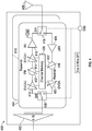
- FIG. 4 illustrates an example beamforming chip architecture 400 with phase shifters and variable gain amplifiers according to an aspect.
- the beamformer chip may include a number of channels. For example, the illustrated embodiments includes 16 channels. Each channel may have a similar architecture or similar components as the channel 404.
- the channel 404 of the beamforming chip 400 can include digital variable gain amplifiers 410, 414, 420, a power amplifier 416, phase shifters 412, 422, a low noise amplifier 424, switches 408, 418, a power divider 402, and a channel memory 426.
- the beamforming chip can set the phase of the signals by sending a phase calibration signal to the phase shifters 412, 422 from the phase configuration table corresponding to the channel.
- the beamforming chip can set the gain of the signals by sending a gain calibration signal to the variable gain amplifiers 410, 414, 420 from the gain configuration table corresponding to the channel.
- the channel memory 426 can include the gain configuration table and/or the phase configuration table corresponding to the channel.
- the power divider 402 can divide input power to 16 channels in the transmit mode and/or combine receiver channel power into 1 output channel in the receive mode.
- the beamforming chip architecture 400 can communicate with an antenna element 406.
- a power divider 402 (or other component such as an adder or splitter) for digital signal processing.
- the signals from the digital signal processor can be sent to a switch 408, which can switch the route of the signals to be transmitted instead of being received by the transceiver.
- a signal on the transmit path may be processed by one or more digital variable gain amplifiers 410, 414, a phase shifter 412, and a power amplifier 416. Then, the signal can be provided to the switch 418 that connects the transmit path with the antenna element 406.
- the signal can be received by the antenna element 406, and the switch 418 can propagate the signal through the receive path.
- the receive path may include a low noise amplifier 424, a phase shifter 422, and a digital variable gain amplifier 420.
- the switch 408 may connect the receive path to the power divider 402 for further signal processing.
- the controller for the antenna array can transmit a signal to a variable gain amplifier corresponding to the channel to adjust the gain of the channel based on the portion of the gain configuration table copied into the channel memory.
- the controller for the antenna array can transmit a signal to a phase shifter corresponding to the channel to adjust the phase of the channel based on the retrieved portion of the phase table.
- FIG. 5 illustrates an example beamforming chip architecture 500 with channels on a single semiconductor chip according to certain aspects.
- a user can program a desired gain and/or phase for each of the channels.
- the user can input the desired gain and/or phase to the single semiconductor chip 502 via an interface, such as a Serial Peripheral Interface (SPI) bus 504.
- SPI Serial Peripheral Interface
- measurements of each channel's gain and phase are stored in Non-Volatile Memory (NVM) 506.
- NVM Non-Volatile Memory
- the measured channel gain for each channel can be subtracted from a reference gain via a corresponding subtractor 508A, 508C, 508E to generate a gain address offset.
- the reference gain can be stored in the NVM 506.
- the measured channel phase for each channel can be subtracted from a reference phase via a corresponding subtractor 508B, 508D, 508F to generate a phase address offset.
- the reference phase can be stored in the NVM 506.
- the gain address offset can be used to determine a start address for copying a portion of a variable gain amplifier configuration attenuation table (or the global gain table 514 stored in the global memory 510).
- the start address can correspond to an entry in the variable gain amplifier configuration attenuation table for a particular gain or a gain attenuation value based on a difference between a reference gain and a maximum gain for the channel. For example, if the difference between the reference gain and the measured gain for a particular channel is 0 (or about 0), the start address may correspond to the address indicating a gain attenuation value of 0 dB.
- a processor or controller may copy a portion of the variable gain amplifier configuration attenuation table starting at the start address and ending at an address that reflects the total gain range of the channel.
- the phase address offset can be used to determine a start address for copying a portion of a phase shifter configuration table (or the global phase table 512 stored in the global memory 510).
- the start address can correspond to a difference in the reference phase and a measured phase for the channel. For example, if the reference phase is 0 (or about 0) and the measured phase is 0 (or about 0), then the start address can correspond to 0 degrees. Is some cases, the entire phase calibration table is copied because all phase values may be supported. However, the starting address of the phase calibration table may vary based on differences between the reference phase and the channel phase at the selected reference setting. The portion of the phase shifter configuration table that is copied can start at the start address and continue through 360 degrees.
- the start address can be 350 degrees.
- the copied portion of the phase shifter configuration table can include 350 and 355, and then wrap back around to 0 degrees.
- the copied portion of the phase shifter configuration table can start at 350, continue to 355, 0, 5, 10, 15... and wrap around to 345.
- the copied portions of the variable gain amplifier configuration attenuation table and the phase shifter configuration table can be stored in the corresponding channel memories.
- the copied portions of the variable gain amplifier configuration attenuation table for channel 1 can be stored into the gain table #1 522A in the channel memory 518A for channel 1.
- the copied portions of the phase shifter configuration table for channel 1 can be stored into the phase table #1 520A in the channel memory 518A for channel 1.
- the copied portions of the variable gain amplifier configuration attenuation table for channel 2 can be stored into the gain table #2 522B in the channel memory 518B for channel 2.
- the copied portions of the phase shifter configuration table for channel 2 can be stored into the phase table #2 520B in the channel memory 518B for channel 2.
- the copied portions of the variable gain amplifier configuration attenuation table for channel N can be stored into the gain table #N 522N in the channel memory 518N for channel N.
- the copied portions of the phase shifter configuration table for channel N can be stored into the phase table #N 520N in the channel memory 518N for channel N.
- the copied portions of the variable gain amplifier configuration attenuation table can be used to determine the change in the variable gain amplifier 524A, 524B, 524N for the corresponding channels.
- the copied portions of the phase shifter configuration table can be used to determine the change in the phase shifter 516A, 516B, 516N for the corresponding channels.
- any of the principles and advantages discussed herein can be implemented in connection with any other systems, apparatus, or methods that benefit could from any of the teachings herein.
- any of the principles and advantages discussed herein can be implemented in connection with any devices with a need to adjust the amplitude or phase of a phased array.
- aspects of this disclosure can be implemented in various electronic devices.
- one or more of the above phased array aspects can be implemented in accordance with any of the principles and advantages discussed herein can be included in various electronic devices.
- the electronic devices can include, but are not limited to, cell phone base stations, radar systems, radar detectors, consumer electronic products, parts of the consumer electronic products such as semiconductor die and/or packaged modules, electronic test equipment, etc.
- Examples of the electronic devices can also include communication networks.
- the consumer electronic products can include, but are not limited to, a phone such as a smart phone, a laptop computer, a tablet computer, a wearable computing device such as a smart watch or an ear piece, an automobile, a camcorder, a camera, a digital camera, a portable memory chip, a washer, a dryer, a washer/dryer, a copier, a facsimile machine, a scanner, a multifunctional peripheral device, a wireless access point, a router, etc.
- the electronic device can include unfinished products, including those for industrial and/or medical applications.
Landscapes
- Engineering & Computer Science (AREA)
- Physics & Mathematics (AREA)
- Computer Networks & Wireless Communication (AREA)
- Signal Processing (AREA)
- Electromagnetism (AREA)
- Radar, Positioning & Navigation (AREA)
- Remote Sensing (AREA)
- General Physics & Mathematics (AREA)
- Nonlinear Science (AREA)
- Variable-Direction Aerials And Aerial Arrays (AREA)
Abstract
Description
- The present application is related to
U.S. Patent Application No. 15/904,045, filed February 23, 2018 U.S. Patent Application No. 16/178,303, filed November 1, 2018 U.S. Provisional Patent Application No. 62/818,397 - The present disclosure relates to an antenna array, in particular to calibration of the antenna array.
- An antenna with a single antenna element will typically broadcast a radiation pattern that radiates equally in all directions in a spherical wavefront. Phased antenna arrays generally refer to a collection of antenna elements that may be used to focus electromagnetic energy in a particular direction creating a main beam. Phased antenna arrays are being used more frequently in a myriad of different applications, such as in military applications, mobile technology, on airplane radar technology, automotive radars, cellular telephone and data, and Wi-Fi technology.
- The individual antenna elements of a phased-antenna array may radiate in a spherical pattern, but collectively generate a wavefront in a particular direction through constructive and destructive interference. The relative phases of the signal transmitted at each antenna element can be either fixed or adjusted, allowing the antenna system to steer the wavefront in different directions. A phased-antenna array typically includes an oscillator, a plurality of antenna elements, a phase adjuster or shifter, a variable gain amplifier, a receiver, and a control processor. A phased antenna array system uses phase adjusters or shifters to control the phase of the signal transmitted by an antenna element. The radiated patterns of the antenna elements constructively interfere in a particular direction creating a wavefront in that direction, which may sometimes be referred to as the main beam. The phased array can realize increased gain and improved signal to noise ratio in the direction of the main beam. The radiation pattern may destructively interfere in one or more additional directions other than the direction of the main beam, and can reduce gain in those directions.
- The amplitude of the signals emanating from the antenna elements affects the side lobe levels, where the side lobes are lobes of the radiation pattern that are not in the direction of the main lobe. It is generally preferable to reduce side lobe levels such that the antenna system can focus transmission in a particular desired direction. As such, the precision of the relative phase and amplitude for the elements determine the precision of the beam direction and the side lobe levels, respectively. Thus, the accuracy of the control of the phase shift and amplitude for the collection of antenna elements is important to the implementation of the phased array.
- The innovations described in the claims each have several aspects, no single one of which is solely responsible for the desirable attributes. Without limiting the scope of the claims, some prominent features of this disclosure will now be briefly described.
- Some aspects include a controller configured to calibrate a beamforming integrated circuit, the controller comprising: a non-volatile memory configured to store measured gain data for a plurality of channels of a beamforming integrated circuit; and calibration circuitry configured to: determine a reference gain value based at least in part on the measured gain data for the plurality of channels stored at the non-volatile memory; and for each channel of the plurality of channels: determine a difference between a maximum gain value of the channel obtain from the non-volatile memory and the reference gain value; and copy a portion of a variable gain amplifier configuration attenuation table stored in a shared memory of the beamforming integrated circuit to a channel memory associated with the channel, wherein the variable gain amplifier configuration attenuation table comprises configuration settings for variable gain amplifiers of the beamforming integrated circuit, and wherein the portion of the variable gain amplifier configuration attenuation table copied from the shared memory starts at an address corresponding to the difference between the maximum gain value of the channel and the reference gain value.
- In some aspects, at least one channel supports a different maximum gain value than at least one other channel of the plurality of channels.
- In some aspects, each channel of the plurality of channels supports a maximum gain value.
- In some aspects, at least one channel of the plurality of channels supports a different maximum gain value.
- In some aspects, the reference gain value comprises a lowest common value among a set of maximum gain values supported by the plurality of channels, wherein the set of maximum gain values comprises maximum gain values supported by at least one of the plurality of channels.
- In some aspects, the non-volatile memory is further configured to store measured phase data for the plurality of channels, wherein the calibration circuitry is further configured to: determine a reference phase value based at least in part on the measured phase data for the plurality of channels stored at the non-volatile memory; and for each channel of the plurality of channels: determine a difference between a phase value of the channel obtain from the non-volatile memory and the reference phase value; and copy a portion of a phase shifter configuration table stored in the shared memory of the beamforming integrated circuit to the channel memory associated with the channel, wherein the phase shifter configuration table comprises configuration settings for phase shifters of the beamforming integrated circuit, and wherein the portion of the phase shifter configuration table copied from the shared memory starts at an address corresponding to the difference between the phase value of the channel and the reference phase value.
- In some aspects, the reference gain value is stored in volatile memory.
- In some aspects, the shared memory is a volatile memory.
- In some aspects, the channel memory corresponding to each of the plurality of channels is a volatile memory.
- Some aspects include a method for calibrating a beamforming integrated circuit, the method comprising: storing, in a non-volatile memory, measured gain data for a plurality of channels of a beamforming integrated circuit; and determining, by calibration circuitry, a reference gain value based at least in part on the measured gain data for the plurality of channels stored at the non-volatile memory; and for each channel of the plurality of channels: determining a difference between a maximum gain value of the channel obtain from the non-volatile memory and the reference gain value; and copying a portion of a variable gain amplifier configuration attenuation table stored in a shared memory of the beamforming integrated circuit to a channel memory associated with the channel, wherein the variable gain amplifier configuration attenuation table comprises configuration settings for variable gain amplifiers of the beamforming integrated circuit, and wherein the portion of the variable gain amplifier configuration attenuation table copied from the shared memory starts at an address corresponding to the difference between the maximum gain value of the channel and the reference gain value.
- In some aspects, at least one channel supports a different maximum gain value than at least one other channel of the plurality of channels.
- In some aspects, each channel of the plurality of channels supports a maximum gain value.
- In some aspects, at least one channel of the plurality of channels supports a different maximum gain value.
- In some aspects, the reference gain value comprises a lowest common value among a set of maximum gain values supported by the plurality of channels, wherein the set of maximum gain values comprises maximum gain values supported by at least one of the plurality of channels.
- In some aspects, the method further comprises: storing, in the non-volatile memory, measured phase data for the plurality of channels; determining a reference phase value based at least in part on the measured phase data for the plurality of channels stored at the non-volatile memory; and for each channel of the plurality of channels: determining a difference between a phase value of the channel obtain from the non-volatile memory and the reference phase value; and copying a portion of a phase shifter configuration table stored in the shared memory of the beamforming integrated circuit to the channel memory associated with the channel, wherein the phase shifter configuration table comprises configuration settings for phase shifters of the beamforming integrated circuit, and wherein the portion of the phase shifter configuration table copied from the shared memory starts at an address corresponding to the difference between the phase value of the channel and the reference phase value.
- In some aspects, the reference gain value is stored in volatile memory.
- In some aspects, the shared memory is a volatile memory.
- In some aspects, the channel memory corresponding to each of the plurality of channels is a volatile memory.
- Some aspects include a controller configured to calibrate a beamforming integrated circuit, the controller comprising: calibration circuitry configured to: determine a reference gain value based at least in part on measured gain data for the plurality of channels stored at a non-volatile memory; and for each channel of the plurality of channels: copy a portion of a variable gain amplifier configuration attenuation table stored in a shared memory of the beamforming integrated circuit to a channel memory associated with the channel, wherein the variable gain amplifier configuration attenuation table comprises configuration settings for variable gain amplifiers of the beamforming integrated circuit, and wherein the portion of the variable gain amplifier configuration attenuation table copied from the shared memory starts at an address corresponding to a difference between a maximum gain value of the channel obtain from the non-volatile memory and the reference gain value.
- In some aspects, the reference gain value is stored in volatile memory.
- For the purposes of summarizing the disclosure, certain aspects, advantages and novel features of the innovations have been described herein. It is to be understood that not necessarily all such advantages may be achieved in accordance with any particular aspect. Thus, the innovations may be embodied or carried out in a manner that achieves or optimizes one advantage or group of advantages as taught herein without necessarily achieving other advantages as may be taught or suggested herein.
- These drawings and the associated description herein are provided to illustrate specific aspects and are not intended to be limiting.
-
Figure 1 illustrates an example memory architecture for a beamforming chip according to certain aspects. -
Figure 2 illustrates an example of the use of a variable gain amplifier configuration table for configuration of variable gain amplifiers for each of the channels of a beamforming chip according to certain aspects. -
Figure 3 illustrates an example of the use of a phase shifter configuration table for configuration of phase shifters for each of the channels of the beamforming chip according to certain aspects. -
Figure 4 illustrates an example beamforming chip architecture with phase shifters and variable gain amplifiers according to certain aspects. -
Figure 5 illustrates an example beamforming chip architecture with channels on a single semiconductor chip according to certain aspects. - The following detailed description of certain aspects presents various descriptions of specific aspects. However, the innovations described herein can be embodied in a multitude of different ways, for example, as defined and covered by the claims. In this description, reference is made to the drawings where like reference numerals can indicate identical or functionally similar elements. It will be understood that elements illustrated in the figures are not necessarily drawn to scale. Moreover, it will be understood that certain aspects can include more elements than illustrated in a drawing and/or a subset of the elements illustrated in a drawing. Further, some aspects can incorporate any suitable combination of features from two or more drawings. The headings provided herein are for convenience only and do not necessarily affect the meaning or scope of the claims.
- An antenna array can enable a beamformer to steer or focus an electromagnetic radiation pattern in a particular direction. The beamformer may generate a main beam in a particular direction and may generate side lobes in other directions. The main beam of the radiation pattern may be generated based on constructive inference of a plurality of signals output by an antenna array. The plurality of signals may be aligned by modifying the phases of at least some of the transmitted signal. Furthermore, the side-lobe levels may be controlled by adjusting the phases and amplitudes of the signals output by the antenna elements. A beamformer can generate a desired antenna pattern by, for example, configuring one or more phase shifter settings and/or one or more variable gain amplifiers to modify the phase and amplitude of signals output by the antenna elements of the beamformer antenna array. Differences in the channels due, for example, to imperfections in the materials or inconsistencies in the manufacturing process may cause inconsistencies in the output of signals from different antennas of the antenna array. Thus the resultant phase and/or output signal strength of the main lobe and side lobes may not match desired specifications. Further, over time, degradation may occur in the channels. To address the inaccuracies innate in the manufacturing process, calibration is often performed in an attempt to align the channels. To perform the calibration, it is desirable to accurately measure and control the phase and amplitude of antenna elements in an array system. The calibration process can be labor intensive, time consuming, and costly. Thus, there is a need for a method of calibration that can be performed without expensive test equipment and facilities. Systems and methods disclosed herein may be applicable during the manufacturing test process and can be used to speed up production and lower costs. However, techniques disclosed herein may also be applied subsequent to manufacture, such as during incorporation into a device by a third-party or during use of the beamformer. In some aspects, the calibration data may be used by the beamformer in combination with other data, such as pre-calculated or pre-stored antenna pattern data, to generate appropriate or desired settings for particular beamforming implementations or use-cases.
- Traditional calibration techniques may use additional circuitry within the antenna array system to capture measurement data, which may be used during calibration. However, such implementations typically require changes to the PCB board to incorporate additional antenna elements and components for calibration of the signal paths, which may cause complications in certain use cases, such as when used with radar systems.
- The maximum supported gain and/or the gain range may vary across different channels of the antenna array. Further, the phase for each channel may also differ for different channels of the antenna array. In other words, when the beaformer is configured to transmit at 0 degrees, two channels may communicate at two slightly different angles due to differences between the channels. The variance in the gain and/or phase of the different channels may occur due, for example, to variance in fabrication, which may be due to differences or imperfections in manufacturing conditions, manufacturing process, or materials.
- The present disclosure provides systems and methods for calibration of antenna arrays. These antenna arrays may be used in a variety of technologies, such as fifth generation cellular technology (5G), radar, or any other application of phased antenna arrays. The present disclosure enables an antenna array system to perform calibration using raw measurements of phase and/or amplitude data. The raw measurements of phase and/or amplitude can be stored in a non-volatile memory. Thus, calibration can be performed, and the performance variance between components on different channels of a transceiver, receiver, or a transmitter can be accounted for during operation of the beamformer based on raw measurements of signals transmitted using the beamformer. In some aspects, the raw measurements of gain and/or phase of a channel in the beamformer can be measured by equipment external to the antenna array system and stored in a memory of the beamformer, such as a non-volatile memory, disposed within the antenna array system. Advantageously, in certain implementations, the antenna array system of the present disclosure does not require substantial hardware modifications for calibration. The antenna array system can store the raw measurements of each channel of the antenna array in a non-volatile memory for persistent storage, and the measurements may be retrieved and used for calibration as needed or desired.
- In some aspects, systems and methods of the present disclosure include storing measurements of a maximum supported gain and/or a deviation from a reference phase for channels of a beamforming chip that can be used to control a beamforming chip. The beamforming chips may include aspects of beamforming chips described in
U.S. Patent Application No. 15/904,045, filed February 23, 2018 U.S. Patent Application No. 16/178,303, filed November 1, 2018 U.S. Patent Application No. 16/178,303 . The measurements may be stored in a non-volatile memory, and a controller can use the data to calibrate the channels of the beamforming chip.Figure 1 illustrates anexample memory architecture 100 for the beamforming chip according to certain aspects. - In some aspects, the phase and gain measurements of each of the channels of the beamforming chip can be stored in non-volatile memory (NVM) 104. The beamforming chip can identify a reference gain and/or
phase 106. The reference gain and/orphase 106 can be used to determine a relative variance across the channels of the measured gain and/or phase stored in thenon-volatile memory 104. The reference gain and reference phase may be stored within thenon-volatile memory 104. Alternatively, the reference gain and/orphase 106 can be stored in volatile or static memory, such as RAM memory. In some aspects, the reference gain and reference phase may be stored within a bypass register or SRAM register of the non-volatile memory. Thus, in certain aspects, the reference gain and reference phase may be stored within a volatile portion of a non-volatile memory system. - In some aspects, the reference gain and/or
phase 106 can be subtracted via asubtractor 108 from the corresponding measurements of gain and/or phase for each of the channels of the beamforming chip can be stored innon-volatile memory 104. Thesubtractor 108 may include or be a substractor. Alternatively, in certain aspects, thesubtractor 108 may include or be replaced by alternative digital logic structures for subtracting the reference gain and/orphase 106 from measurement of gain and/or phase for each of the channels of the beamforming chip. For example, thesubtractor 108 may include or be replaced with any type of logic that may be generated by a logic design tool, such as an automatic logic generator. In some aspects, the reference gain can include a gain measurement of a channel, or be derived from a gain measurement of a channel. - In some aspects, the reference gain and/or
phase 106 can be based on the measurements of gain and/or phase for one or more of the channels of the beamforming chip, and can be stored innon-volatile memory 104. In the example ofFigure 1 , the antenna array can include 16 channels, each corresponding to a maximum gain value for the corresponding channel. The reference gain can include a lowest common maximum gain value for the channels of the beamforming chip system. The reference gain value can be subtracted from the corresponding actual measurements of gain and/or phase for each of the channels of the antenna array and can be stored innon-volatile memory 104. For example for a 2 channel antenna array, ifchannel 0 has a maximum gain of 20 dB andchannel 1 has a maximum gain of 22 dB, the reference gain may be designated as 20 dB as it is the lower maximum among the two channels. It may be desirable to identify the maximum gain that is commonly supported among a set of channels in order to limit a gain of the beamforming chip to a value that can be supported by all channels within the beamformer. For instance, in the previous example it may be undesirable to select a gain of 21 dB because althoughchannel 1 may support such a gain value,channel 0 may not. The measurements of maximum gain supported by the channels of the beamforming chip may be obtained during a manufacturing and/or testing process performed with respect to the beamforming chip. It should be understood that each beamforming chip may have different measured maximum gain values due to, for example, variations that may occur during the manufacturing process. - In some aspects, the reference phase may be selected as an arbitrary angle, for example 0 degrees, 45 degrees, 90 degrees, etc. that can be used to align each of the channels during a calibration process. For example, if the reference phase is specified to be 0 degrees, a measurement of the phase of an output signal may be obtained when the input phase of the signal is 0 degrees. For instance, when the channel is set to the desired reference phase of 0 degrees, it may be determined through measurement of the output signal that due, for example, to process variations that the output signal is at 1 degree or 5 degrees. This measurement of phase for each channel may be stored in the
NVM 104. When attempting to calibrate the beamforming chip, the measured phase may be subtracted from the selected reference phase (or vice versa) of 0 degrees to obtain an index value for indexing a portion of a phase calibration table stored in aglobal memory 110. Thisglobal memory 110 may be shared among channels of the beamforming chip, or in some cases, among multiple beamforming chips. In some aspects, the reference phase can include a phase measurement of a channel, or be derived from a phase measurement of a channel. - In some aspects, the
global memory 110 can be used to retrieve calibration data for each of the channels. Theglobal memory 110 can be a volatile or static memory. Theglobal memory 110 can be used to retrieve gain and/or phase values for each of thechannel memory 102. Theglobal memory 110 can store a variable gain amplifier configuration table, where the variable gain amplifier configuration table stores configuration settings for variable gain amplifiers of a beamforming integrated circuit. The configuration settings can include an attenuation value for the variable gain amplifier for reducing gain from a maximum supported gain to a desired gain. For instance, with reference toFigure 2 , if the desired gain is the common maximum supported gain, then the attenuation value stored at an address associated with the common maximum supported gain (in this case address 0) may be applied to a set of variable gain amplifiers associated with the beamformer channels. In the illustrated example ofFigure 2 , the maximum supported gain ofchannel 0 and of the beamformer are the same. Thus, the attenuation value stored ataddress 0 of the memory associated withchannel 0 is 0 dB. However, the maximum supported gain ofchannel 1 is 2 dB greater than the common maximum supported gain of the beamformer. Thus, the attenuation value stored ataddress 0 of the memory associated withchannel 1 is 2 dB. Theglobal memory 110 can store a phase shifter configuration table, where the phase shifter configuration table stores configuration settings for phase shifters of a beamforming integrated circuit. The configuration settings can include a phase degree for shifting the phase of a signal. - In some aspects, a portion of the
global memory 110 can be copied to corresponding channels of thechannel memory 102 as illustrated inFigure 2 . The portion of theglobal memory 110 copied to thechannel memory 102 may differ for each channel of the beamforming chip based, at least in part, on a difference between the supported gain of the channel and the reference gain, and/or the difference between a measured phase of the channel and a reference phase when the channel is set at the reference phase. The portion of theglobal memory 110 copied to the channel memory may be associated with the supported gain range of the beamforming chip. Further, the portion of theglobal memory 110 copied to thechannel memory 102 may differ for each channel based at least in part on a difference between the reference gain and the maximum supported gain of the channel. Thus, for example, while each channel may receive the same number of entries from theglobal memory 110, such as 20, 22, or 25 entries, the entries received may differ for at least some of the channels based on the maximum supported gain of the channel and the reference gain. The portion copied from the variable gain amplifier configuration table of the global memory can start at a start address corresponding to the difference between the maximum gain of the corresponding channel and thereference gain value 106 and may continue for a number of entries associated with the gain range for the beamforming chip. In some aspects, the start address can be derived based on the difference between the maximum gain of the corresponding channel and thereference gain value 106. - Similarly in some respects to the gain amplifier configuration table, a portion of the phase shifter configuration table may be copied from the global memory beginning at a start address corresponding to the difference between the phase offset of the corresponding channel and the
reference phase value 106. However, in certain aspects, unlike the gain amplifier configuration table, because a particular channel may support a full 360 degrees, the entire table may be copied with the value associated with the first entry in the calibration table copied to channel memory being selected from the global memory based at least in part on the difference between the reference phase and the measured phase when the channel is configured with the reference phase. In other words, in some cases an entry ataddress 0 may serve as a start address for a first channel while an entry ataddress 1 may server as a start address for a second channel with the entry ataddress 0 being the last entry copied to the channel memory. Another example of the copying of the phase table is illustrated with respect toFigure 3 . - In the example of
Figure 1 , the antenna array includes 16 channels. In other aspects, the antenna array can include more or less channels. The channels can include circuitry to adjust the gain of a signal traveling through the corresponding channel. The channels can include circuitry to adjust the phase of a signal traveling through the corresponding channel. For example, one or more channels can include a variable gain amplifier and/or a phase shifter for adjusting the gain and/or phase, respectively, of the corresponding channel. - In some aspects, the beamforming chip can include a
channel memory 102 for each of the channels. Thechannel memory 102 can include gain setting data for the circuitry to adjust the gain, such as a variable gain amplifier. The gain setting data can be used to control the adjustment of gain within the variable gain amplifier. For example, the gain setting data can include a certain amount of signal attenuation for the variable gain amplifier. In some aspects, thechannel memory 102 can include phase setting data for the circuitry to adjust the phase, such as a phase shifter. The phase setting data can be used to control the adjustment of phase within the phase shifter. The phase setting data can include a certain amount of phase offset for the phase shifter. For example, assume the maximum gain forchannel 0 is 20 dB and forchannel 1 is 22 dB. If, in this example, the desired gain is 18 dB, then a particular address (e.g., address 2) of the channel memory for each channel may be selected. Forchannel 0,address 2 may indicate an attenuation of 2 dB to reduce the 20 dB gain to 18 dB. However, forchannel 1, theaddress 2 may indicate an attenuation of 4 dB to reduce the 22 dB gain to 18 dB. Thus, despite different supported maximum gains, both channels can be attenuated to the same gain value when accessing the same address in the correspondingchannel memory 102 for the channel. - In some aspects, the
channel memory 102 can adjust for variances between channels, such as variances in components, signal mismatches, signal degradation, and/or the like. Thechannel memory 102 can be a volatile or static memory. -
Figure 2 illustrates an example 200 of the use of a variable gain amplifier configuration table for configuration of variable gain amplifiers for each of the channels of the beamforming chip according to certain aspects. - In the example of
Figure 2 , maximum gain across channels of a beamforming chip may vary. For instance the gain across channels may vary from 20 to 26 dB. In one non-limiting example, the gain range may be 34 dB and the VGAs may be capable of adjusting gain in 1 dB steps. In this example, 6 dB of the gain range may be reserved for calibration. So after calibration, the gain range may be 28 dB. - In some aspects, channel 0 (ch0) has a maximum gain of 20 dB, and channel 1 (ch1) has a maximum gain of 22 dB. The other channels of the beamforming chip have maximum gains higher than 20 dB. The reference gain can be identified as 20 dB, as the lowest maximum gain across all channels. In some aspects, the reference gain can be a desired gain, such as a minimum gain to receive and/or transmit a certain target or signal.
- In some aspects, the reference gain can be subtracted from the maximum gain of the channel. For channel 0 (ch0), the reference gain of 20 dB can be subtracted from the maximum gain of 20 dB. Accordingly, the portion of the gain configuration table 202 stored in the global memory can be copied to the channel 0 (ch0)
memory 204, starting from the address that corresponds to the 0 dB attenuation. Because the gain range is 28 dB, the copied portion can start at the address corresponding to 0 dB attenuation (address 0 in the global memory 202) and go up to 28 dB (address 28 in the global memory 202), the gain range. The portion copied into thechannel 0memory 204 can be copied such that the address corresponding to the 0 dB attenuation is the starting address (address 0) in thechannel 0memory 204, and the address corresponding to the 28 dB attenuation is the last address (address 28) in thechannel 0memory 204. Likewise, the channel 1 (ch1)memory 206 can be populated based on a maximum gain of 22 dB. - In some aspects, for channel 1 (ch1), the reference gain of 20 dB can be subtracted from the maximum gain of 22 dB. Accordingly, another portion of the gain configuration table 202 stored in the global memory can be copied to the channel 1 (ch1)
memory 206, starting from the address that corresponds to the 2 dB attenuation, which was the difference between the reference gain of 20 dB and the maximum gain of 22 dB forchannel 1. Because the gain range is 28 dB, the copied portion can start at the starting address corresponding to 2 dB attenuation (address 2 in the global memory 202) and can end at an end address of 30 dB (address 30 in the global memory 202), the range of the gain supported bychannel 1. The portion copied into thechannel 1memory 206 can be copied such that the address corresponding to the 2 dB attenuation is the starting address (address 0) in thechannel 1memory 206, and the address corresponding to the 30 dB attenuation is the last address (address 28) in thechannel 1memory 206. Advantageously, even if the supported gain across different channels varies, the channel gain for each channel can be adjusted to account for these variations. -
Figure 3 illustrates an example 300 of the use of a phase shifter configuration table for configuration of phase shifters for each of the channels of the beamforming chip according to an aspect. - In some cases, the actual phase for each channel may vary when the beamformer is configured to transmit a signal at a particular phase. This variance in phase may, similarly to the variance in gain, be attributable to differences in channels due to the manufacturing process or non-uniformity in the materials (e.g., semiconductor dies). For instance, with reference to the tables in
Figure 3 , when the phase is set to 0degrees channel 0 may be at 0 degrees whilechannel 1 may be around 12 degrees. In some cases, the reference phase may be set to 0 degrees. However, the present disclosure is not limited as such, and other phase values may be used. - In some aspects, the reference phase can be subtracted from the measured phase of the channel. For channel 0 (ch0), the reference phase of 0 degrees can be subtracted from the measured phase of 0 degrees. Accordingly, the portion of the phase configuration table 302 stored in the global memory can be copied to the channel 0 (ch0)
memory 304, starting from the address that corresponds to the 0 degrees. - In the illustrated implementation of
Figure 3 , the granularity of phase adjustments may be 5.625 degrees in this particular non-limiting example. Thus, 64 entries can be copied intochannel 0 table 304. The copied portion can start at the address corresponding to 0 degrees (address 0 in the global memory 302) and go up to 354.375 degrees (address 63 in the global memory 302). The copied portion into thechannel 0memory 304 can be copied such that the address corresponding to 0 degrees is the starting address (address 0) in thechannel 0memory 304, and the address corresponding to the 374.375 is the last address (address 63) in thechannel 0memory 304. Likewise, the channel 1 (ch1)memory 306 can be populated based theglobal memory 302. However, in the illustrated example,channel 1 may have a measured phase difference of 12 degrees compared tochannel 0. In some implementations, the phase ofchannel 1 may be adjusted by 348 degrees such thatchannel 1 andchannel 0 are both at 0 degrees. In the illustrated example, the phase ofchannel 1 may be adjusted by 348.75 degrees due to step-size granularity or resolution being in increments of 5.625 degrees. In some cases, a more fine granularity may be used. However, in such cases, the amount of memory required to store the calibration table is increased. - In some aspects, for channel 1 (ch1), the reference phase of 0 degrees can be subtracted from the measured phase of 12 degrees. Accordingly, another portion of the phase configuration table 302 stored in the global memory can be copied to the channel 1 (ch1)
memory 306, starting from the address that corresponds to the 348.75 degrees, which was the difference between the reference phase of 0 degrees and the measured of 12 degrees forchannel 1. The system can identify that 348.75 degrees is to the closest degree to 348 degrees, which corresponds to -12 degrees (the difference between 0 and 12 degrees). - In some aspects, because the resolution is 5.625 degrees, the copied portion can start at the address corresponding to 3478.75 degrees (
address 62 in the global memory 202) and go up to the last entry in the global memory 302 (address 63), continue from the first address in the global memory 302 (address 0), and up to 343.125 degrees (address 61), totaling 63 addresses. The copied portion into thechannel 1memory 306 can be copied such that the address corresponding to the 348.75 degrees is the starting address (address 0) in thechannel 1memory 306, and the address corresponding to the 343.125 degrees is the last address (address 63) in thechannel 1memory 306. -
Figure 4 illustrates an examplebeamforming chip architecture 400 with phase shifters and variable gain amplifiers according to an aspect. The beamformer chip may include a number of channels. For example, the illustrated embodiments includes 16 channels. Each channel may have a similar architecture or similar components as thechannel 404. Thechannel 404 of thebeamforming chip 400 can include digitalvariable gain amplifiers power amplifier 416,phase shifters low noise amplifier 424, switches 408, 418, apower divider 402, and achannel memory 426. The beamforming chip can set the phase of the signals by sending a phase calibration signal to thephase shifters variable gain amplifiers channel memory 426 can include the gain configuration table and/or the phase configuration table corresponding to the channel. Thepower divider 402 can divide input power to 16 channels in the transmit mode and/or combine receiver channel power into 1 output channel in the receive mode. In some aspects, thebeamforming chip architecture 400 can communicate with anantenna element 406. - In some aspects, there are 16
channels 404 that feed into a power divider 402 (or other component such as an adder or splitter) for digital signal processing. The signals from the digital signal processor can be sent to aswitch 408, which can switch the route of the signals to be transmitted instead of being received by the transceiver. A signal on the transmit path may be processed by one or more digitalvariable gain amplifiers phase shifter 412, and apower amplifier 416. Then, the signal can be provided to theswitch 418 that connects the transmit path with theantenna element 406. - In some aspects, if the switch is switched to the receive path, the signal can be received by the
antenna element 406, and theswitch 418 can propagate the signal through the receive path. The receive path may include alow noise amplifier 424, aphase shifter 422, and a digitalvariable gain amplifier 420. Theswitch 408 may connect the receive path to thepower divider 402 for further signal processing. - In some aspects, the controller for the antenna array can transmit a signal to a variable gain amplifier corresponding to the channel to adjust the gain of the channel based on the portion of the gain configuration table copied into the channel memory. The controller for the antenna array can transmit a signal to a phase shifter corresponding to the channel to adjust the phase of the channel based on the retrieved portion of the phase table.
-
Figure 5 illustrates an examplebeamforming chip architecture 500 with channels on a single semiconductor chip according to certain aspects. In some aspects, a user can program a desired gain and/or phase for each of the channels. The user can input the desired gain and/or phase to thesingle semiconductor chip 502 via an interface, such as a Serial Peripheral Interface (SPI)bus 504. - In some aspects, measurements of each channel's gain and phase are stored in Non-Volatile Memory (NVM) 506. In the example of
Figure 5 , there are N total channels, where N may include any positive integer. For instance, there may be 1, 2, 4, 8, 16, 24, 32, 64 channels, any number of channels between the preceding examples, or more channels. The measured channel gain for each channel can be subtracted from a reference gain via acorresponding subtractor NVM 506. The measured channel phase for each channel can be subtracted from a reference phase via acorresponding subtractor NVM 506. - In some aspects, the gain address offset can be used to determine a start address for copying a portion of a variable gain amplifier configuration attenuation table (or the global gain table 514 stored in the global memory 510). The start address can correspond to an entry in the variable gain amplifier configuration attenuation table for a particular gain or a gain attenuation value based on a difference between a reference gain and a maximum gain for the channel. For example, if the difference between the reference gain and the measured gain for a particular channel is 0 (or about 0), the start address may correspond to the address indicating a gain attenuation value of 0 dB. A processor or controller may copy a portion of the variable gain amplifier configuration attenuation table starting at the start address and ending at an address that reflects the total gain range of the channel.
- In some aspects, the phase address offset can be used to determine a start address for copying a portion of a phase shifter configuration table (or the global phase table 512 stored in the global memory 510). The start address can correspond to a difference in the reference phase and a measured phase for the channel. For example, if the reference phase is 0 (or about 0) and the measured phase is 0 (or about 0), then the start address can correspond to 0 degrees. Is some cases, the entire phase calibration table is copied because all phase values may be supported. However, the starting address of the phase calibration table may vary based on differences between the reference phase and the channel phase at the selected reference setting. The portion of the phase shifter configuration table that is copied can start at the start address and continue through 360 degrees. For example, if the reference phase is 0 degrees and the measured phase is 10 degrees, the start address can be 350 degrees. With a resolution of 5 degrees for the phase shifter configuration table, the copied portion of the phase shifter configuration table can include 350 and 355, and then wrap back around to 0 degrees. Thus, the copied portion of the phase shifter configuration table can start at 350, continue to 355, 0, 5, 10, 15... and wrap around to 345.
- In some aspects, the copied portions of the variable gain amplifier configuration attenuation table and the phase shifter configuration table can be stored in the corresponding channel memories. For example, the copied portions of the variable gain amplifier configuration attenuation table for
channel 1 can be stored into thegain table # 1 522A in thechannel memory 518A forchannel 1. The copied portions of the phase shifter configuration table forchannel 1 can be stored into thephase table # 1 520A in thechannel memory 518A forchannel 1. The copied portions of the variable gain amplifier configuration attenuation table forchannel 2 can be stored into thegain table # 2 522B in thechannel memory 518B forchannel 2. The copied portions of the phase shifter configuration table forchannel 2 can be stored into thephase table # 2 520B in thechannel memory 518B forchannel 2. The copied portions of the variable gain amplifier configuration attenuation table for channel N can be stored into the gaintable #N 522N in thechannel memory 518N for channel N. The copied portions of the phase shifter configuration table for channel N can be stored into the phasetable #N 520N in thechannel memory 518N for channel N. - In some aspects, the copied portions of the variable gain amplifier configuration attenuation table can be used to determine the change in the
variable gain amplifier phase shifter - Any of the principles and advantages discussed herein can be applied to other systems, not just to the systems described above. Some aspects can include a subset of features and/or advantages set forth herein. The elements and operations of the various aspects described above can be combined to provide further aspects. The acts of the methods discussed herein can be performed in any order as appropriate. Moreover, the acts of the methods discussed herein can be performed serially or in parallel, as appropriate. While circuits are illustrated in particular arrangements, other equivalent arrangements are possible.
- Any of the principles and advantages discussed herein can be implemented in connection with any other systems, apparatus, or methods that benefit could from any of the teachings herein. For instance, any of the principles and advantages discussed herein can be implemented in connection with any devices with a need to adjust the amplitude or phase of a phased array.
- Aspects of this disclosure can be implemented in various electronic devices. For instance, one or more of the above phased array aspects can be implemented in accordance with any of the principles and advantages discussed herein can be included in various electronic devices. Examples of the electronic devices can include, but are not limited to, cell phone base stations, radar systems, radar detectors, consumer electronic products, parts of the consumer electronic products such as semiconductor die and/or packaged modules, electronic test equipment, etc. Examples of the electronic devices can also include communication networks. The consumer electronic products can include, but are not limited to, a phone such as a smart phone, a laptop computer, a tablet computer, a wearable computing device such as a smart watch or an ear piece, an automobile, a camcorder, a camera, a digital camera, a portable memory chip, a washer, a dryer, a washer/dryer, a copier, a facsimile machine, a scanner, a multifunctional peripheral device, a wireless access point, a router, etc. Further, the electronic device can include unfinished products, including those for industrial and/or medical applications.
- Unless the context clearly requires otherwise, throughout the description and the claims, the words "comprise," "comprising," "include," "including," and the like are to be construed in an inclusive sense, as opposed to an exclusive or exhaustive sense; that is to say, in the sense of "including, but not limited to." The words "coupled" or "connected", as generally used herein, refer to two or more elements that may be either directly connected, or connected by way of one or more intermediate elements. Thus, although the various schematics shown in the figures depict example arrangements of elements and components, additional intervening elements, devices, features, or components may be present in an actual aspect (assuming that the functionality of the depicted circuits is not adversely affected). Additionally, the words "herein," "above," "below," and words of similar import, when used in this application, shall refer to this application as a whole and not to any particular portions of this application. Where the context permits, words in the Detailed Description of Certain Aspects using the singular or plural number may also include the plural or singular number, respectively. The words "or" in reference to a list of two or more items, is intended to cover all of the following interpretations of the word: any of the items in the list, all of the items in the list, and any combination of the items in the list. All numerical values or distances provided herein are intended to include similar values within a measurement error.
- While certain aspects have been described, these aspects have been presented by way of example only, and are not intended to limit the scope of the disclosure. Indeed, the novel apparatus, systems, and methods described herein may be embodied in a variety of other forms. Furthermore, various omissions, substitutions and changes in the form of the methods and systems described herein may be made without departing from the spirit of the disclosure. The accompanying claims and their equivalents are intended to cover such forms or modifications as would fall within the scope and spirit of the disclosure.
Claims (15)
- A controller configured to calibrate a beamforming integrated circuit, the controller comprising:a non-volatile memory configured to store measured gain data for a plurality of channels of a beamforming integrated circuit; andcalibration circuitry configured to:determine a reference gain value based at least in part on the measured gain data for the plurality of channels stored at the non-volatile memory; andfor each channel of the plurality of channels:determine a difference between a maximum gain value of the channel obtain from the non-volatile memory and the reference gain value; andcopy a portion of a variable gain amplifier configuration attenuation table stored in a shared memory of the beamforming integrated circuit to a channel memory associated with the channel, wherein the variable gain amplifier configuration attenuation table comprises configuration settings for variable gain amplifiers of the beamforming integrated circuit, and wherein the portion of the variable gain amplifier configuration attenuation table copied from the shared memory starts at an address corresponding to the difference between the maximum gain value of the channel and the reference gain value.
- The controller of claim 1, wherein at least one channel supports a different maximum gain value than at least one other channel of the plurality of channels.
- The controller of claim 1, wherein each channel of the plurality of channels supports a maximum gain value, and wherein preferably at least one channel of the plurality of channels supports a different maximum gain value.
- The controller of any preceding claim, wherein the reference gain value comprises a lowest common value among a set of maximum gain values supported by the plurality of channels, wherein the set of maximum gain values comprises maximum gain values supported by at least one of the plurality of channels.
- The controller of any preceding claim, wherein the non-volatile memory is further configured to store measured phase data for the plurality of channels, wherein the calibration circuitry is further configured to:determine a reference phase value based at least in part on the measured phase data for the plurality of channels stored at the non-volatile memory; andfor each channel of the plurality of channels:determine a difference between a phase value of the channel obtain from the non-volatile memory and the reference phase value; andcopy a portion of a phase shifter configuration table stored in the shared memory of the beamforming integrated circuit to the channel memory associated with the channel, wherein the phase shifter configuration table comprises configuration settings for phase shifters of the beamforming integrated circuit, and wherein the portion of the phase shifter configuration table copied from the shared memory starts at an address corresponding to the difference between the phase value of the channel and the reference phase value.
- The controller of any preceding claim, wherein the reference gain value is stored in volatile memory.
- The controller of any preceding claim, wherein the shared memory and/or the channel memory corresponding to each of the plurality of channels is a volatile memory.
- A method for calibrating a beamforming integrated circuit, the method comprising:storing, in a non-volatile memory, measured gain data for a plurality of channels of a beamforming integrated circuit; anddetermining, by calibration circuitry, a reference gain value based at least in part on the measured gain data for the plurality of channels stored at the non-volatile memory; andfor each channel of the plurality of channels:determining a difference between a maximum gain value of the channel obtain from the non-volatile memory and the reference gain value; andcopying a portion of a variable gain amplifier configuration attenuation table stored in a shared memory of the beamforming integrated circuit to a channel memory associated with the channel, wherein the variable gain amplifier configuration attenuation table comprises configuration settings for variable gain amplifiers of the beamforming integrated circuit, and wherein the portion of the variable gain amplifier configuration attenuation table copied from the shared memory starts at an address corresponding to the difference between the maximum gain value of the channel and the reference gain value.
- The method of claim 8, wherein at least one channel supports a different maximum gain value than at least one other channel of the plurality of channels.
- The method of claim 8, wherein each channel of the plurality of channels supports a maximum gain value, and wherein preferably at least one channel of the plurality of channels supports a different maximum gain value.
- The method of any of claims 8 to 10, wherein the reference gain value comprises a lowest common value among a set of maximum gain values supported by the plurality of channels, wherein the set of maximum gain values comprises maximum gain values supported by at least one of the plurality of channels.
- The method of any of claims 8 to 11, wherein the method further comprises:storing, in the non-volatile memory, measured phase data for the plurality of channels;determining a reference phase value based at least in part on the measured phase data for the plurality of channels stored at the non-volatile memory; andfor each channel of the plurality of channels:determining a difference between a phase value of the channel obtain from the non-volatile memory and the reference phase value; andcopying a portion of a phase shifter configuration table stored in the shared memory of the beamforming integrated circuit to the channel memory associated with the channel, wherein the phase shifter configuration table comprises configuration settings for phase shifters of the beamforming integrated circuit, and wherein the portion of the phase shifter configuration table copied from the shared memory starts at an address corresponding to the difference between the phase value of the channel and the reference phase value.
- The method of any of claims 8 to 12, wherein the reference gain value is stored in volatile memory.
- The method of any of claims 8 to 13, wherein the shared memory and/or the channel memory corresponding to each of the plurality of channels is a volatile memory.
- A controller configured to calibrate a beamforming integrated circuit, the controller comprising:
calibration circuitry configured to:determine a reference gain value based at least in part on measured gain data for the plurality of channels stored at a non-volatile memory, wherein preferably the reference gain value is stored in volatile memory; andfor each channel of the plurality of channels:
copy a portion of a variable gain amplifier configuration attenuation table stored in a shared memory of the beamforming integrated circuit to a channel memory associated with the channel, wherein the variable gain amplifier configuration attenuation table comprises configuration settings for variable gain amplifiers of the beamforming integrated circuit, and wherein the portion of the variable gain amplifier configuration attenuation table copied from the shared memory starts at an address corresponding to a difference between a maximum gain value of the channel obtain from the non-volatile memory and the reference gain value.
Applications Claiming Priority (2)
| Application Number | Priority Date | Filing Date | Title |
|---|---|---|---|
| US201962818397P | 2019-03-14 | 2019-03-14 | |
| US16/748,030 US11404779B2 (en) | 2019-03-14 | 2020-01-21 | On-chip phased array calibration systems and methods |
Publications (3)
| Publication Number | Publication Date |
|---|---|
| EP3709538A1 true EP3709538A1 (en) | 2020-09-16 |
| EP3709538C0 EP3709538C0 (en) | 2023-06-07 |
| EP3709538B1 EP3709538B1 (en) | 2023-06-07 |
Family
ID=69770633
Family Applications (1)
| Application Number | Title | Priority Date | Filing Date |
|---|---|---|---|
| EP20160945.0A Active EP3709538B1 (en) | 2019-03-14 | 2020-03-04 | On-chip phased array calibration |
Country Status (3)
| Country | Link |
|---|---|
| US (1) | US11404779B2 (en) |
| EP (1) | EP3709538B1 (en) |
| KR (1) | KR102645972B1 (en) |
Families Citing this family (3)
| Publication number | Priority date | Publication date | Assignee | Title |
|---|---|---|---|---|
| US12609741B2 (en) * | 2023-07-17 | 2026-04-21 | International Business Machines Corporation | Configurable beamformer integrated circuit control |
| US12580613B2 (en) | 2024-02-06 | 2026-03-17 | International Business Machines Corporation | Arbitrary spatial filters based on beam transformation |
| WO2025235714A1 (en) * | 2024-05-09 | 2025-11-13 | Ohio State Innovation Foundation | Systems and methods of calibrating a phased array antenna |
Citations (2)
| Publication number | Priority date | Publication date | Assignee | Title |
|---|---|---|---|---|
| EP2285102A2 (en) * | 2007-03-14 | 2011-02-16 | Fresco Microchip | A universal television receiver |
| WO2018119153A2 (en) * | 2016-12-21 | 2018-06-28 | Intel Corporation | Wireless communication technology, apparatuses, and methods |
Family Cites Families (79)
| Publication number | Priority date | Publication date | Assignee | Title |
|---|---|---|---|---|
| US4864315A (en) | 1985-11-05 | 1989-09-05 | Itt Avionics | Phased array antenna testing arrangement |
| US5412414A (en) | 1988-04-08 | 1995-05-02 | Martin Marietta Corporation | Self monitoring/calibrating phased array radar and an interchangeable, adjustable transmit/receive sub-assembly |
| US5235342A (en) | 1989-08-30 | 1993-08-10 | Gec-Marconi, Ltd. | Antenna array with system for locating and adjusting phase centers of elements of the antenna array |
| US5581517A (en) | 1994-08-05 | 1996-12-03 | Acuson Corporation | Method and apparatus for focus control of transmit and receive beamformer systems |
| US5657023A (en) | 1996-05-02 | 1997-08-12 | Hughes Electronics | Self-phase up of array antennas with non-uniform element mutual coupling and arbitrary lattice orientation |
| KR100206468B1 (en) * | 1996-05-31 | 1999-07-01 | 윤종용 | Output controlling apparatus and method of mobile communication system |
| US5864543A (en) | 1997-02-24 | 1999-01-26 | At&T Wireless Services, Inc. | Transmit/receive compensation in a time division duplex system |
| US6104935A (en) | 1997-05-05 | 2000-08-15 | Nortel Networks Corporation | Down link beam forming architecture for heavily overlapped beam configuration |
| US5864317A (en) | 1997-05-23 | 1999-01-26 | Raytheon Company | Simplified quadrant-partitioned array architecture and measure sequence to support mutual-coupling based calibration |
| US6208287B1 (en) | 1998-03-16 | 2001-03-27 | Raytheoncompany | Phased array antenna calibration system and method |
| US6252542B1 (en) | 1998-03-16 | 2001-06-26 | Thomas V. Sikina | Phased array antenna calibration system and method using array clusters |
| CN1118146C (en) | 1999-08-10 | 2003-08-13 | 信息产业部电信科学技术研究院 | Method and device for calibrating intelligent antenna array |
| KR100382454B1 (en) | 1999-12-15 | 2003-05-09 | 니폰덴신뎅와 가부시키가이샤 | Adaptive array antenna transmitting/receiving apparatus |
| US6356233B1 (en) | 2000-12-12 | 2002-03-12 | Lockheed Martin Corporation | Structure for an array antenna, and calibration method therefor |
| US6507315B2 (en) | 2001-05-03 | 2003-01-14 | Lockheed Martin Corporation | System and method for efficiently characterizing the elements in an array antenna |
| DE10237823B4 (en) | 2002-08-19 | 2004-08-26 | Kathrein-Werke Kg | Antenna array with a calibration device and method for operating such an antenna array |
| WO2004025321A1 (en) | 2002-09-11 | 2004-03-25 | Lockheed Martin Corporation | Cce calibration with an array of calibration probes interleaved with the array antenna |
| US7362266B2 (en) | 2004-12-07 | 2008-04-22 | Lockheed Martin Corporation | Mutual coupling method for calibrating a phased array |
| JP4531607B2 (en) | 2005-03-30 | 2010-08-25 | 富士通株式会社 | Calibration device |
| JP4478606B2 (en) | 2005-05-19 | 2010-06-09 | 富士通株式会社 | Calibration apparatus and calibration method for linear array antenna |
| US7904117B2 (en) | 2005-08-12 | 2011-03-08 | Sibeam | Wireless communication device using adaptive beamforming |
| US7471237B2 (en) | 2006-03-22 | 2008-12-30 | The Boeing Company | Built-in missile RADAR calibration verification |
| US7714776B2 (en) | 2006-06-27 | 2010-05-11 | National University Of Ireland Maynooth | Antenna array calibration |
| US7576686B2 (en) | 2006-08-07 | 2009-08-18 | Garmin International, Inc. | Method and system for calibrating an antenna array for an aircraft surveillance system |
| US20080129613A1 (en) | 2006-12-05 | 2008-06-05 | Nokia Corporation | Calibration for re-configurable active antennas |
| US8559571B2 (en) | 2007-08-17 | 2013-10-15 | Ralink Technology Corporation | Method and apparatus for beamforming of multi-input-multi-output (MIMO) orthogonal frequency division multiplexing (OFDM) transceivers |
| WO2009027724A1 (en) | 2007-08-31 | 2009-03-05 | Bae Systems Plc | Antenna calibration |
| US7714775B2 (en) | 2007-12-17 | 2010-05-11 | The Boeing Company | Method for accurate auto-calibration of phased array antennas |
| EP2173010A1 (en) | 2008-10-02 | 2010-04-07 | Nokia Siemens Networks OY | Improved probe calibration for an active antenna |
| US8045926B2 (en) | 2008-10-15 | 2011-10-25 | Nokia Siemens Networks Oy | Multi-transceiver architecture for advanced Tx antenna monitoring and calibration in MIMO and smart antenna communication systems |
| US8193971B2 (en) | 2008-11-10 | 2012-06-05 | Motorola Mobility, Inc. | Antenna reciprocity calibration |
| GB2467773B (en) | 2009-02-13 | 2012-02-01 | Socowave Technologies Ltd | Communication system, apparatus and methods for calibrating an antenna array |
| GB2467772B (en) | 2009-02-13 | 2012-05-02 | Socowave Technologies Ltd | Communication system, network element and method for antenna array calibration |
| US7911376B2 (en) | 2009-04-01 | 2011-03-22 | Sony Corporation | Systems and methods for antenna array calibration |
| US8660500B2 (en) | 2009-06-09 | 2014-02-25 | Broadcom Corporation | Method and system for a voltage-controlled oscillator with a leaky wave antenna |
| US8154452B2 (en) | 2009-07-08 | 2012-04-10 | Raytheon Company | Method and apparatus for phased array antenna field recalibration |
| EP2372836B1 (en) | 2010-03-18 | 2017-05-03 | Alcatel Lucent | Antenna array calibration |
| US9444577B1 (en) | 2010-04-05 | 2016-09-13 | Marvell International Ltd. | Calibration correction for implicit beamformer using an explicit beamforming technique in a wireless MIMO communication system |
| US8897717B2 (en) | 2010-07-28 | 2014-11-25 | Honeywell International Inc. | Dual-feed antenna array with integral comparison circuit for phase and amplitude calibration |
| GB2485543B (en) | 2010-11-17 | 2014-03-12 | Socowave Technologies Ltd | Mimo antenna calibration device,integrated circuit and method for compensating phase mismatch |
| JP5246250B2 (en) | 2010-12-09 | 2013-07-24 | 株式会社デンソー | Phased array antenna phase calibration method and phased array antenna |
| JP5104938B2 (en) | 2010-12-09 | 2012-12-19 | 株式会社デンソー | Phased array antenna phase calibration method and phased array antenna |
| US8199048B1 (en) | 2010-12-15 | 2012-06-12 | University Of Massachusetts | Calibration technique for phased array antennas |
| JP6174574B2 (en) | 2011-06-02 | 2017-08-02 | パーカーヴィジョン インコーポレイテッド | Antenna control |
| US9154969B1 (en) | 2011-09-29 | 2015-10-06 | Marvell International Ltd. | Wireless device calibration for implicit transmit |
| US9124361B2 (en) | 2011-10-06 | 2015-09-01 | Raytheon Company | Scalable, analog monopulse network |
| US9041602B2 (en) | 2011-11-14 | 2015-05-26 | Earl W. McCune, Jr. | Phased array transmission methods and apparatus |
| US9130271B2 (en) | 2012-02-24 | 2015-09-08 | Futurewei Technologies, Inc. | Apparatus and method for an active antenna system with near-field radio frequency probes |
| CN104718713B (en) | 2012-09-13 | 2019-01-01 | 爱立信(中国)通信有限公司 | Method and apparatus for antenna calibration |
| CA2831325A1 (en) | 2012-12-18 | 2014-06-18 | Panasonic Avionics Corporation | Antenna system calibration |
| US9813129B2 (en) | 2013-01-28 | 2017-11-07 | Tubis Technology | Hierarchically elaborated phased-array antenna modules and faster beam steering method of operation |
| GB2517217B (en) | 2013-08-16 | 2018-03-21 | Analog Devices Global | Communication unit, integrated circuit and method for generating a plurality of sectored beams |
| GB2517218B (en) | 2013-08-16 | 2017-10-04 | Analog Devices Global | Communication unit and method of antenna array calibration |
| US9735899B2 (en) | 2013-09-30 | 2017-08-15 | Vayyar Imaging Ltd. | Device and method for calibrating antenna array systems |
| FR3012683B1 (en) | 2013-10-29 | 2017-03-10 | Commissariat Energie Atomique | CALIBRATION OF ANTENNA NETWORK |
| GB2519946A (en) | 2013-10-29 | 2015-05-13 | Socowave Technologies Ltd | Active antenna system and methods of testing |
| KR101564730B1 (en) | 2013-12-27 | 2015-10-30 | 한화탈레스 주식회사 | Method for arranging array plane of phase array antenna |
| US10056685B2 (en) | 2014-03-06 | 2018-08-21 | Samsung Electronics Co., Ltd. | Antenna array self-calibration |
| US9331751B2 (en) | 2014-08-05 | 2016-05-03 | Raytheon Company | Method and system for characterizing an array antenna using near-field measurements |
| US9614279B2 (en) | 2014-08-11 | 2017-04-04 | Raytheon Company | Portable apparatus and associated method for phased array field calibration |
| WO2017001013A1 (en) | 2015-07-01 | 2017-01-05 | Telefonaktiebolaget Lm Ericsson (Publ) | Technique for calibrating an antenna array |
| US9912467B2 (en) | 2015-09-22 | 2018-03-06 | Qualcomm Incorporated | Full duplex technique |
| GB2543563B (en) | 2015-10-23 | 2020-02-12 | Cambium Networks Ltd | Method and Apparatus for Controlling Equivalent Isotropic Radiated Power |
| JP6561867B2 (en) | 2016-02-15 | 2019-08-21 | 株式会社デンソー | Multiple transmitting antenna phase calibration device |
| EP3427417B1 (en) | 2016-03-07 | 2022-05-11 | Satixfy UK Limited | Calibration techniques for an antenna array |
| US9705611B1 (en) | 2016-03-24 | 2017-07-11 | Rockwell Collins, Inc. | Systems and methods for array antenna calibration |
| US10103431B2 (en) | 2016-04-21 | 2018-10-16 | Google Llc | Phased array antenna calibration |
| US10484106B2 (en) | 2016-05-05 | 2019-11-19 | International Business Machines Corporation | Antenna calibration |
| US10148366B2 (en) | 2016-07-29 | 2018-12-04 | Rohde & Schwarz Gmbh & Co. Kg | Calibration systems and methods |
| EP3484070B1 (en) | 2016-07-30 | 2021-05-19 | Huawei Technologies Co., Ltd. | Method and device for calibrating antenna array |
| US20180062260A1 (en) * | 2016-08-26 | 2018-03-01 | Analog Devices Global | Antenna array calibration systems and methods |
| US9876514B1 (en) | 2016-08-31 | 2018-01-23 | Anokiwave, Inc. | Calibration of active electronically steered antennas using on-chip programming |
| US10211527B2 (en) | 2016-10-21 | 2019-02-19 | C-Com Satellite Systems Inc. | Method and apparatus for phased antenna array calibration |
| EP3596780B1 (en) | 2017-03-13 | 2021-06-30 | Telefonaktiebolaget LM Ericsson (PUBL) | Self-calibration of antenna array system |
| US10128894B1 (en) | 2017-05-09 | 2018-11-13 | Analog Devices Global | Active antenna calibration |
| US10305564B1 (en) | 2017-11-13 | 2019-05-28 | Loon Llc | Beamforming calibration |
| US10305608B1 (en) | 2017-11-13 | 2019-05-28 | Loon Llc | Beamforming calibration |
| US11177567B2 (en) | 2018-02-23 | 2021-11-16 | Analog Devices Global Unlimited Company | Antenna array calibration systems and methods |
| TWI678846B (en) | 2018-11-15 | 2019-12-01 | 財團法人工業技術研究院 | Antenna device and method for calibrating antenna device |
-
2020
- 2020-01-21 US US16/748,030 patent/US11404779B2/en active Active
- 2020-02-25 KR KR1020200022906A patent/KR102645972B1/en active Active
- 2020-03-04 EP EP20160945.0A patent/EP3709538B1/en active Active
Patent Citations (2)
| Publication number | Priority date | Publication date | Assignee | Title |
|---|---|---|---|---|
| EP2285102A2 (en) * | 2007-03-14 | 2011-02-16 | Fresco Microchip | A universal television receiver |
| WO2018119153A2 (en) * | 2016-12-21 | 2018-06-28 | Intel Corporation | Wireless communication technology, apparatuses, and methods |
Also Published As
| Publication number | Publication date |
|---|---|
| EP3709538C0 (en) | 2023-06-07 |
| US20200295456A1 (en) | 2020-09-17 |
| KR20200110609A (en) | 2020-09-24 |
| US11404779B2 (en) | 2022-08-02 |
| EP3709538B1 (en) | 2023-06-07 |
| KR102645972B1 (en) | 2024-03-08 |
Similar Documents
| Publication | Publication Date | Title |
|---|---|---|
| US11811147B2 (en) | Method for calibrating phased array antenna and related apparatus | |
| US12095171B2 (en) | Antenna array calibration systems and methods | |
| US11177567B2 (en) | Antenna array calibration systems and methods | |
| US11404779B2 (en) | On-chip phased array calibration systems and methods | |
| US10670712B2 (en) | Methods and apparatus for a MIMO radar | |
| CN108880703B (en) | Active antenna calibration | |
| US10797807B2 (en) | Methods for calibrating millimeter wave antenna arrays | |
| US11158940B2 (en) | Self-calibration of antenna array system | |
| JP5815448B2 (en) | Phased array transmitter | |
| CN1078390C (en) | Antenna array calibration | |
| CN104335507B (en) | Phased Array Transmitter | |
| US20100127932A1 (en) | Method of calibrating an active antenna and active antenna | |
| CN112073097A (en) | Self-calibration device for hybrid beam forming receiving array | |
| US20120178395A1 (en) | Dynamic Impedance Matching with LNA | |
| US20230361888A1 (en) | Calibration circuit for calibrating phases and gains between channels in multi-channel beamforming system, multi-channel beamforming system including the same and channel calibration method using the same | |
| US11450952B2 (en) | Beamformer automatic calibration systems and methods | |
| US11329376B2 (en) | Beamforming device, calibration method and calibration system for the same | |
| CN115882971B (en) | Phased array antenna calibration method, device, electronic device, and readable storage medium | |
| US11239552B2 (en) | Beamforming device, calibration method and calibration system for the same | |
| JP2016225845A (en) | Phased array transmitter | |
| CN112213701B (en) | Radar near-field azimuth calculation method, device, terminal and storage medium | |
| RU2647514C2 (en) | Method and device for calibrating transceiving active phased antenna array | |
| TWI773982B (en) | Beamforming device, calibration method and calibration system for the same | |
| JP7672357B2 (en) | Wireless communication device and calibration method | |
| CN115225126B (en) | Uplink sending method, ABF module, terminal and storage medium |
Legal Events
| Date | Code | Title | Description |
|---|---|---|---|
| PUAI | Public reference made under article 153(3) epc to a published international application that has entered the european phase |
Free format text: ORIGINAL CODE: 0009012 |
|
| STAA | Information on the status of an ep patent application or granted ep patent |
Free format text: STATUS: THE APPLICATION HAS BEEN PUBLISHED |
|
| AK | Designated contracting states |
Kind code of ref document: A1 Designated state(s): AL AT BE BG CH CY CZ DE DK EE ES FI FR GB GR HR HU IE IS IT LI LT LU LV MC MK MT NL NO PL PT RO RS SE SI SK SM TR |
|
| AX | Request for extension of the european patent |
Extension state: BA ME |
|
| STAA | Information on the status of an ep patent application or granted ep patent |
Free format text: STATUS: REQUEST FOR EXAMINATION WAS MADE |
|
| 17P | Request for examination filed |
Effective date: 20210219 |
|
| RBV | Designated contracting states (corrected) |
Designated state(s): AL AT BE BG CH CY CZ DE DK EE ES FI FR GB GR HR HU IE IS IT LI LT LU LV MC MK MT NL NO PL PT RO RS SE SI SK SM TR |
|
| GRAP | Despatch of communication of intention to grant a patent |
Free format text: ORIGINAL CODE: EPIDOSNIGR1 |
|
| STAA | Information on the status of an ep patent application or granted ep patent |
Free format text: STATUS: GRANT OF PATENT IS INTENDED |
|
| INTG | Intention to grant announced |
Effective date: 20220601 |
|
| GRAJ | Information related to disapproval of communication of intention to grant by the applicant or resumption of examination proceedings by the epo deleted |
Free format text: ORIGINAL CODE: EPIDOSDIGR1 |
|
| STAA | Information on the status of an ep patent application or granted ep patent |
Free format text: STATUS: REQUEST FOR EXAMINATION WAS MADE |
|
| GRAP | Despatch of communication of intention to grant a patent |
Free format text: ORIGINAL CODE: EPIDOSNIGR1 |
|
| STAA | Information on the status of an ep patent application or granted ep patent |
Free format text: STATUS: GRANT OF PATENT IS INTENDED |
|
| INTC | Intention to grant announced (deleted) | ||
| INTG | Intention to grant announced |
Effective date: 20221019 |
|
| GRAS | Grant fee paid |
Free format text: ORIGINAL CODE: EPIDOSNIGR3 |
|
| GRAA | (expected) grant |
Free format text: ORIGINAL CODE: 0009210 |
|
| STAA | Information on the status of an ep patent application or granted ep patent |
Free format text: STATUS: THE PATENT HAS BEEN GRANTED |
|
| AK | Designated contracting states |
Kind code of ref document: B1 Designated state(s): AL AT BE BG CH CY CZ DE DK EE ES FI FR GB GR HR HU IE IS IT LI LT LU LV MC MK MT NL NO PL PT RO RS SE SI SK SM TR |
|
| REG | Reference to a national code |
Ref country code: GB Ref legal event code: FG4D |
|
| REG | Reference to a national code |
Ref country code: CH Ref legal event code: EP Ref country code: AT Ref legal event code: REF Ref document number: 1577939 Country of ref document: AT Kind code of ref document: T Effective date: 20230615 Ref country code: DE Ref legal event code: R096 Ref document number: 602020011478 Country of ref document: DE |
|
| U01 | Request for unitary effect filed |
Effective date: 20230621 |
|
| U07 | Unitary effect registered |
Designated state(s): AT BE BG DE DK EE FI FR IT LT LU LV MT NL PT SE SI Effective date: 20230628 |
|
| REG | Reference to a national code |
Ref country code: LT Ref legal event code: MG9D |
|
| PG25 | Lapsed in a contracting state [announced via postgrant information from national office to epo] |
Ref country code: NO Free format text: LAPSE BECAUSE OF FAILURE TO SUBMIT A TRANSLATION OF THE DESCRIPTION OR TO PAY THE FEE WITHIN THE PRESCRIBED TIME-LIMIT Effective date: 20230907 Ref country code: ES Free format text: LAPSE BECAUSE OF FAILURE TO SUBMIT A TRANSLATION OF THE DESCRIPTION OR TO PAY THE FEE WITHIN THE PRESCRIBED TIME-LIMIT Effective date: 20230607 |
|
| PG25 | Lapsed in a contracting state [announced via postgrant information from national office to epo] |
Ref country code: RS Free format text: LAPSE BECAUSE OF FAILURE TO SUBMIT A TRANSLATION OF THE DESCRIPTION OR TO PAY THE FEE WITHIN THE PRESCRIBED TIME-LIMIT Effective date: 20230607 Ref country code: HR Free format text: LAPSE BECAUSE OF FAILURE TO SUBMIT A TRANSLATION OF THE DESCRIPTION OR TO PAY THE FEE WITHIN THE PRESCRIBED TIME-LIMIT Effective date: 20230607 Ref country code: GR Free format text: LAPSE BECAUSE OF FAILURE TO SUBMIT A TRANSLATION OF THE DESCRIPTION OR TO PAY THE FEE WITHIN THE PRESCRIBED TIME-LIMIT Effective date: 20230908 |
|
| PG25 | Lapsed in a contracting state [announced via postgrant information from national office to epo] |
Ref country code: SK Free format text: LAPSE BECAUSE OF FAILURE TO SUBMIT A TRANSLATION OF THE DESCRIPTION OR TO PAY THE FEE WITHIN THE PRESCRIBED TIME-LIMIT Effective date: 20230607 |
|
| PG25 | Lapsed in a contracting state [announced via postgrant information from national office to epo] |
Ref country code: IS Free format text: LAPSE BECAUSE OF FAILURE TO SUBMIT A TRANSLATION OF THE DESCRIPTION OR TO PAY THE FEE WITHIN THE PRESCRIBED TIME-LIMIT Effective date: 20231007 |
|
| PG25 | Lapsed in a contracting state [announced via postgrant information from national office to epo] |
Ref country code: SM Free format text: LAPSE BECAUSE OF FAILURE TO SUBMIT A TRANSLATION OF THE DESCRIPTION OR TO PAY THE FEE WITHIN THE PRESCRIBED TIME-LIMIT Effective date: 20230607 Ref country code: SK Free format text: LAPSE BECAUSE OF FAILURE TO SUBMIT A TRANSLATION OF THE DESCRIPTION OR TO PAY THE FEE WITHIN THE PRESCRIBED TIME-LIMIT Effective date: 20230607 Ref country code: RO Free format text: LAPSE BECAUSE OF FAILURE TO SUBMIT A TRANSLATION OF THE DESCRIPTION OR TO PAY THE FEE WITHIN THE PRESCRIBED TIME-LIMIT Effective date: 20230607 Ref country code: IS Free format text: LAPSE BECAUSE OF FAILURE TO SUBMIT A TRANSLATION OF THE DESCRIPTION OR TO PAY THE FEE WITHIN THE PRESCRIBED TIME-LIMIT Effective date: 20231007 Ref country code: CZ Free format text: LAPSE BECAUSE OF FAILURE TO SUBMIT A TRANSLATION OF THE DESCRIPTION OR TO PAY THE FEE WITHIN THE PRESCRIBED TIME-LIMIT Effective date: 20230607 |
|
| PG25 | Lapsed in a contracting state [announced via postgrant information from national office to epo] |
Ref country code: PL Free format text: LAPSE BECAUSE OF FAILURE TO SUBMIT A TRANSLATION OF THE DESCRIPTION OR TO PAY THE FEE WITHIN THE PRESCRIBED TIME-LIMIT Effective date: 20230607 |
|
| REG | Reference to a national code |
Ref country code: DE Ref legal event code: R097 Ref document number: 602020011478 Country of ref document: DE |
|
| U20 | Renewal fee for the european patent with unitary effect paid |
Year of fee payment: 5 Effective date: 20240220 |
|
| PLBE | No opposition filed within time limit |
Free format text: ORIGINAL CODE: 0009261 |
|
| STAA | Information on the status of an ep patent application or granted ep patent |
Free format text: STATUS: NO OPPOSITION FILED WITHIN TIME LIMIT |
|
| 26N | No opposition filed |
Effective date: 20240308 |
|
| REG | Reference to a national code |
Ref country code: CH Ref legal event code: PL |
|
| PG25 | Lapsed in a contracting state [announced via postgrant information from national office to epo] |
Ref country code: MC Free format text: LAPSE BECAUSE OF FAILURE TO SUBMIT A TRANSLATION OF THE DESCRIPTION OR TO PAY THE FEE WITHIN THE PRESCRIBED TIME-LIMIT Effective date: 20230607 |
|
| PG25 | Lapsed in a contracting state [announced via postgrant information from national office to epo] |
Ref country code: MC Free format text: LAPSE BECAUSE OF FAILURE TO SUBMIT A TRANSLATION OF THE DESCRIPTION OR TO PAY THE FEE WITHIN THE PRESCRIBED TIME-LIMIT Effective date: 20230607 |
|
| PG25 | Lapsed in a contracting state [announced via postgrant information from national office to epo] |
Ref country code: IE Free format text: LAPSE BECAUSE OF NON-PAYMENT OF DUE FEES Effective date: 20240304 |
|
| PG25 | Lapsed in a contracting state [announced via postgrant information from national office to epo] |
Ref country code: IE Free format text: LAPSE BECAUSE OF NON-PAYMENT OF DUE FEES Effective date: 20240304 Ref country code: CH Free format text: LAPSE BECAUSE OF NON-PAYMENT OF DUE FEES Effective date: 20240331 |
|
| U20 | Renewal fee for the european patent with unitary effect paid |
Year of fee payment: 6 Effective date: 20250210 |
|
| PG25 | Lapsed in a contracting state [announced via postgrant information from national office to epo] |
Ref country code: CY Free format text: LAPSE BECAUSE OF FAILURE TO SUBMIT A TRANSLATION OF THE DESCRIPTION OR TO PAY THE FEE WITHIN THE PRESCRIBED TIME-LIMIT; INVALID AB INITIO Effective date: 20200304 |
|
| PG25 | Lapsed in a contracting state [announced via postgrant information from national office to epo] |
Ref country code: HU Free format text: LAPSE BECAUSE OF FAILURE TO SUBMIT A TRANSLATION OF THE DESCRIPTION OR TO PAY THE FEE WITHIN THE PRESCRIBED TIME-LIMIT; INVALID AB INITIO Effective date: 20200304 |
|
| PG25 | Lapsed in a contracting state [announced via postgrant information from national office to epo] |
Ref country code: TR Free format text: LAPSE BECAUSE OF FAILURE TO SUBMIT A TRANSLATION OF THE DESCRIPTION OR TO PAY THE FEE WITHIN THE PRESCRIBED TIME-LIMIT Effective date: 20230607 |
|
| U20 | Renewal fee for the european patent with unitary effect paid |
Year of fee payment: 7 Effective date: 20260219 |
|
| PGFP | Annual fee paid to national office [announced via postgrant information from national office to epo] |
Ref country code: GB Payment date: 20260219 Year of fee payment: 7 |