EP3709129B1 - Chip reset via communication interface terminals - Google Patents
Chip reset via communication interface terminals Download PDFInfo
- Publication number
- EP3709129B1 EP3709129B1 EP20163094.4A EP20163094A EP3709129B1 EP 3709129 B1 EP3709129 B1 EP 3709129B1 EP 20163094 A EP20163094 A EP 20163094A EP 3709129 B1 EP3709129 B1 EP 3709129B1
- Authority
- EP
- European Patent Office
- Prior art keywords
- signal
- reset
- state
- input
- spi
- Prior art date
- Legal status (The legal status is an assumption and is not a legal conclusion. Google has not performed a legal analysis and makes no representation as to the accuracy of the status listed.)
- Active
Links
Images


Classifications
-
- H—ELECTRICITY
- H03—ELECTRONIC CIRCUITRY
- H03K—PULSE TECHNIQUE
- H03K17/00—Electronic switching or gating, i.e. not by contact-making and –breaking
- H03K17/22—Modifications for ensuring a predetermined initial state when the supply voltage has been applied
-
- G—PHYSICS
- G06—COMPUTING OR CALCULATING; COUNTING
- G06F—ELECTRIC DIGITAL DATA PROCESSING
- G06F1/00—Details not covered by groups G06F3/00 - G06F13/00 and G06F21/00
- G06F1/22—Means for limiting or controlling the pin/gate ratio
-
- G—PHYSICS
- G06—COMPUTING OR CALCULATING; COUNTING
- G06F—ELECTRIC DIGITAL DATA PROCESSING
- G06F1/00—Details not covered by groups G06F3/00 - G06F13/00 and G06F21/00
- G06F1/24—Resetting means
-
- G—PHYSICS
- G06—COMPUTING OR CALCULATING; COUNTING
- G06F—ELECTRIC DIGITAL DATA PROCESSING
- G06F9/00—Arrangements for program control, e.g. control units
- G06F9/06—Arrangements for program control, e.g. control units using stored programs, i.e. using an internal store of processing equipment to receive or retain programs
- G06F9/44—Arrangements for executing specific programs
- G06F9/4401—Bootstrapping
-
- G—PHYSICS
- G06—COMPUTING OR CALCULATING; COUNTING
- G06F—ELECTRIC DIGITAL DATA PROCESSING
- G06F9/00—Arrangements for program control, e.g. control units
- G06F9/06—Arrangements for program control, e.g. control units using stored programs, i.e. using an internal store of processing equipment to receive or retain programs
- G06F9/44—Arrangements for executing specific programs
- G06F9/4401—Bootstrapping
- G06F9/4416—Network booting; Remote initial program loading [RIPL]
-
- H—ELECTRICITY
- H03—ELECTRONIC CIRCUITRY
- H03K—PULSE TECHNIQUE
- H03K19/00—Logic circuits, i.e. having at least two inputs acting on one output; Inverting circuits
- H03K19/20—Logic circuits, i.e. having at least two inputs acting on one output; Inverting circuits characterised by logic function, e.g. AND, OR, NOR, NOT circuits
Definitions
- the present disclosure relates generally to an electronic system and method, and, in particular embodiments, to a chip reset via communication interface terminals.
- a circuit such as a system on chip (SoC) or an application-specific integrated circuit (ASIC), has a supply voltage range in which it operates properly. If the system begins operating when the supply voltage is below the operating range, the system may malfunction.
- SoC system on chip
- ASIC application-specific integrated circuit
- a power management integrated circuit may have an operating supply voltage range from 3 V to 5.5 V. Beginning operation of such PMIC at, e.g., 2 V, may cause such PMIC to startup in an unknown state.
- FIG. 1 shows integrated circuit (IC) 102 receiving a reset signal to place IC 102 in a known state after startup.
- IC integrated circuit
- FIG 1 shows RC circuit 106 is used to keep reset voltage V RST low while the supply voltage V DD increases.
- IC 102 is off while the voltage V RST is low.
- RC circuit 106 is designed such that when the reset voltage V RST increases above the threshold, supply voltage VDD is inside the operating voltage supply range of IC 102.
- some ICs include a power-on reset (POR) to detect that power has been applied to the IC. After detecting that power has been applied, the POR circuit internally generates a reset signal that places the IC in a known state.
- POR power-on reset
- US 2017/185548 A1 describes a transmission system that includes master device and a plurality of slave devices.
- US 5 974 561 A describes a method and apparatus for generating a reset signal within an integrated circuit.
- US 2018/276157 A1 describes a serial peripheral interface daisy chain mode system and apparatus.
- US 2016/349326 A1 describes a debug trigger interface for non-debug domain system reset.
- Embodiments of the present invention will be described in specific contexts, such as a chip reset using SPI terminals. Embodiments not falling within the scope of the claims may be used with other communication protocols, such as joint test action group (JTAG), or other serial or parallel communication protocols, for example.
- JTAG joint test action group
- serial or parallel communication protocols for example.
- an IC is capable of being reset to a known state via SPI terminals.
- an internal POR circuit and a dedicated reset terminal may advantageously be avoided.
- an internal POR circuit some embodiments may advantageously reduce the die area, which may result in lower costs per die.
- a dedicated reset terminal some embodiments may advantageously reduce the package size (e.g., because of lower pin count), which may result in lower package costs.
- FIG. 2 shows a schematic diagram of IC 202 having a chip reset by reusing terminals of a communication interface, such as an SPI interface, according to an embodiment of the present invention.
- IC 202 includes SPI slave 208, which forms the communication interface of IC 202, and input circuit 400.
- SPI slave 208 includes chip select terminal CS_N configured to receive signal V CS_N via which selection and unselection of the SPI slave 208 is carried out, a master-out-slave-in (MOSI) terminal MOSI configured to receive signal V MOSI via which data is received by SPI slave 208, a master-in-slave-out (MISO) terminal MISO configured to generate signal V MISO via which data is sent by SPI slave 208, and a clock terminal SCLK configured to receive signal V SCLK , which serves as a clock signal for SPI bus 206.
- Input circuit 400 is configured to receive first and second signals, which may correspond to signals V CS_N and V MOSI , respectively.
- IC 202 includes terminals SCLK, MISO, MOSI and CS_N that corresponds to terminals SCLK, MISO, MOSI and CS_N of SPI slave 208.
- SPI master 204 may initiate SPI communication with IC 202 via SPI bus 206 and IC 202 may communicate with SPI master 204 via SPI bus 206 using SPI slave 208.
- SPI master 204 may assert (i.e., set in its active state) terminal CS_N to select SPI slave 208 to communicate with SPI slave 208 and deassert (i.e., set in its inactive state) terminal CS_N to unselect SPI slave 208 such that SPI slave 208 ignores the communication from SPI bus 206.
- SPI master 204 may assert CS_N terminal by transitioning signal V CSN from high to low and may deassert CS_N terminal by transitioning signal V CS_N from low to high.
- SPI slave 208 When SPI slave 208 is selected, SPI master 204 generates a clock signal at terminal SCLK at a frequency supported by SPI and sends data to SPI slave 208 via terminal MOSI. SPI slave 208 then processes data transferred from SPI master 204 with signal V MOSI via terminal MOSI (e.g., in case a of write command, write the specified register in a register map of IC 202). If applicable (e.g., when SPI slave 208 receives a read command), SPI slave 208 sends data back to SPI master 204 with signal V MISO via terminal MISO. When terminal CS_N is deasserted (e.g., such as when signal V CS_N is high), SPI slave 208 is unselected.
- terminal CS_N When terminal CS_N is deasserted (e.g., such as when signal V CS_N is high), SPI slave 208 is unselected.
- SPI slave 208 When SPI slave 208 is unselected, SPI slave 208 ignores (i.e., does not process) data from SPI bus 206 (e.g., ignores the toggling of signals V SCLK and V MOSI at terminals SCLK and MOSI).
- SPI master 204 may be, for example, a microcontroller, processor, digital signal processor (DSP), ASIC, or other device having an SPI master interface.
- IC 202 may be a PMIC, ASIC, driver, radar circuit, or any other device having an SPI slave interface.
- SPI slave 208 may be implemented in any way known in the art. In some embodiments, SPI slave 208 supports SPI frequencies higher than 1 MHz, such as 10 MHz, 50 MHz, or higher. Frequencies lower than 1 MHz may also be supported by SPI slave 208.
- the chip select terminal and the master-out-slave-in terminal of an SPI communication bus are used to reset an IC to place the IC in a known state.
- the reset may be issued after power-up (e.g., immediately after power is applied to the IC), or at any time during operation.
- asserting the master-out-slave-in terminal e.g., high causes the IC to reset to a known state.
- the known state of the IC may be a predetermined state, e.g., as defined by default values of a register map of the IC. For example, bits on a register map the IC may configure one or more analog or digital blocks. By resetting the register map to default values and providing such default values to the one or more analog or digital blocks, the IC may be placed in known state.
- Figure 3 shows a waveform diagram illustrating SPI signals of SPI terminals of IC 202, according to an embodiment.
- terminal CS_N when terminal CS_N is deasserted (e.g., high), transitioning terminal MOSI to a low state causes an internal reset signal RESET_N to be asserted (e.g., low). Asserting the internal reset signal RESET_N causes IC 202 to be placed in a known state.
- terminal CS_N When terminal CS_N is asserted, active SPI communication may be ongoing between SPI master 204 and SPI slave 208, and transitioning terminal MOSI to a low state does not change the state of the internal reset signal RESET_N. Changes in the state of terminal MOSI also do not cause a change in the state of the internal reset signal RESET_N during a blanking time T blank after deasserting terminal CS_N.
- blanking time T blank may be between 4 ns and 10 ns. In some embodiments, blanking time T blank may be higher than 10 ns, or lower than 4 ns. In some embodiments, blanking time T blank may be at least as long, or longer, than half a period of the frequency of the communication bus, such as half a period of a clock signal at terminal SCLK.
- the internal reset signal RESET_N is illustrated as an active low signal (i.e., asserted when low and deasserted when high), some embodiments may use a reset signal that is active high (i.e., asserted when high and deasserted when low).
- Advantages of some embodiments include the capability of asynchronously resetting an IC to place it in a known state without using a dedicated reset terminal and without using a POR circuit that is internal to the IC.
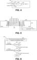
- FIG. 4 shows a schematic diagram of input circuit 400 for generating the internal reset signal RESET_N based on SPI terminals, according to an embodiment of the present invention.
- Input circuit 400 includes delay circuit 402, AND gate 404, NAND gate 406, and inverter 408.
- Input circuit 400 is enabled by default when power is applied to IC 202.
- input circuit may be disabled during normal operation, e.g., when IC 202 goes to a low power mode.
- IC 202 includes additional circuits (not shown), such as an input driver coupled between the chip select terminal CS_N of IC 202 and delay circuit 402, and an input driver coupled between MOSI terminal of IC 202 and AND gate 406, for example. In such embodiments, such input drivers may be enabled by default.
- Delay circuit 402 may be implemented, for example, as a plurality of inverters connected in series. Other implementations are also possible.
- IC 202 may be reset by reusing two terminals of a single SPI communication interface.
- an IC may include a multi-I/O SPI interface, such as a dual SPI interface, quad SPI interface, or octo SPI interface.
- two terminals of such multi-I/O SPI interface may be used to reset the IC to place it in a known state.
- Figure 5 shows a schematic diagram of IC 502, according to an embodiment of the present invention.
- IC 502 includes quad SPI slave 508.
- Quad SPI slave 508 includes chip select terminal CS_N configured to receive signal V CS_N , a input/output terminals IO0, IO1, IO2, and IO3 configured to receive and transmit signals V IO0 , V IO1 , V IO2 , and V IO3 , and a clock terminal SCLK configured to receive signal V SCLK .
- IC 502 includes terminals SCLK, IO0, IO1, IO2, IO3 and CS_N that corresponds to terminals SCLK, IO0, IO1, IO2, IO3 and CS_N of quad SPI slave 508.
- Quad SPI communication bus 506 may have up to 4 times the data bandwidth as a single SPI communication bus 206 when operating at the same SPI clock frequency.
- IC 502 may be reset in a similar manner as IC 202.
- another I/O terminal such as IO2, IO1, or IO0, may be coupled to input circuit 400 used instead of IO3.
- one or more ICs having, e.g., a single SPI interface may be coupled to SPI communication bus 506 without interfering with the reset operation of IC 502.
- Figure 6 shows a schematic diagram of system 600 having IC 502, and having at least one more SPI slave 602 coupled to SPI communication bus 606, according to an embodiment of the present invention.
- SPI slave 602 may operate in a similar manner as SPI slave 208.
- SPI slave 602 when quad SPI slave 508 is not selected (CS_N deasserted), SPI slave 602 may be selected (CS2_N asserted), and SPI master 604 may communicate with SPI slave 602 via SPI communication bus 606 (e.g., using terminals 100 as master-out-slave-in terminal and IO1 as master-in-slave-out terminal).
- SPI communication bus 606 e.g., using terminals 100 as master-out-slave-in terminal and IO1 as master-in-slave-out terminal.
- IC 502 may not be accidentally reset since terminal IO3 is not being used in such communication (i.e., terminal IO3 is not switching during the communication between SPI master 604 and SPI slave 602 via SPI communication bus 606).
- SPI slave 602 Although a single SPI slave 602 is shown coupled to SPI communication bus 606 in Figure 6 , in some embodiments more than one SPI slave may be coupled to SPI communication bus 606.
- an IC having another multi-I/O SPI interface such as an octo SPI interface, may be implemented in a similar manner as IC 502 in system 600.
- FIG. 7 shows a schematic diagram of IC 702 having a chip reset by reusing terminals of a SWD (Serial Wire Debug) interface.
- IC 702 includes SWD interface 708.
- SWD interface 708 includes input clock terminal SWCLK, data in and out terminal SWDIO and serial wire output terminal SWO.
- a reset signal may be generated inside IC 702 without using a dedicated reset terminal by using an input circuit, such as input circuit 400, as shown in Figure 7 .
- Delay circuit 402 may cause a delay of at least a time equal to when SWCLK signal is high (e.g., half a period of SWCLK signal), or longer. Toggling SWCLK during normal debug, therefore, does not cause the internal reset signal RESET_N to be asserted.
- SWCLK is asserted (e.g., high), and SWDIO is asserted for at least a period equal to blanking time T blank .
- SWD is a bidirectional protocol that is generally used for debugging purposes.
- SWCLK terminal is configured to receive a clock signal V SWCLK .
- SWDIO terminal is used to receive and send data by using signal V SWDIO .
- SWO terminal is configured to generate signal V SWO to aid in debug tracing.
- SWD interface 708 may be implemented in any way known in the art.
- Figure 8 shows a flowchart of embodiment method 800 for resetting an integrated circuit, according to an embodiment of the present invention.
- Method 800 may be implemented, for example, by an IC coupled to an SPI communication bus, such as ICs 202 and 502.
- Method 800 may also be implemented, in examples not included in the scope of the claims, by ICs coupled to other types of communication bus, such as IC 702, for example.
- an IC receives first and second signals via first and second terminals of the IC, the first and second terminals of the IC being coupled to first and second terminals of a communication interface of the IC.
- the communication interface is an SPI slave, such as SPI slave 208.
- the first and second signals correspond to signals V CS_N and V MOSI , respectively, and the first and the second terminals correspond to the chip select terminal CS_N and the master-out-slave-in terminal MOSI, respectively.
- the communication interface may be a multi-IO SPI interface, such as SPI slave 508.
- the communication interface may be an SWD interface, such as SWD interface 708. Other communication interfaces may be used.
- a circuit such as input circuit 400 determines the state of the first signal. If the first signal is in a first state of the first signal (e.g., low), the IC returns to step 802. If the first signal is in a second state of the first signal (e.g., high), the input circuit determines the state of the second signal during step 806.
- the IC If the second signal is in a first state of the second signal (e.g., high), the IC returns to step 802. If the second signal is in a second state of the second signal (e.g., low), the IC is reset to a known state during step 808. In some embodiment, the IC is reset when the input circuit asserts a reset signal, such as RESET_N (e.g., transitioning the reset signal from a first state of the reset signal, such as high, to a second state of the reset signal, such as low).
- a reset signal such as RESET_N (e.g., transitioning the reset signal from a first state of the reset signal, such as high, to a second state of the reset signal, such as low).
Landscapes
- Engineering & Computer Science (AREA)
- Theoretical Computer Science (AREA)
- Physics & Mathematics (AREA)
- General Engineering & Computer Science (AREA)
- General Physics & Mathematics (AREA)
- Software Systems (AREA)
- Computer Security & Cryptography (AREA)
- Semiconductor Integrated Circuits (AREA)
- Electronic Switches (AREA)
Description
- The present disclosure relates generally to an electronic system and method, and, in particular embodiments, to a chip reset via communication interface terminals.
- Generally, a circuit, such as a system on chip (SoC) or an application-specific integrated circuit (ASIC), has a supply voltage range in which it operates properly. If the system begins operating when the supply voltage is below the operating range, the system may malfunction. For example, a power management integrated circuit (PMIC) may have an operating supply voltage range from 3 V to 5.5 V. Beginning operation of such PMIC at, e.g., 2 V, may cause such PMIC to startup in an unknown state.
- Circuits generally use a reset signal to bring the system to a defined state during startup. For example,
Figure 1 shows integrated circuit (IC) 102 receiving a reset signal to placeIC 102 in a known state after startup. As shown inFigure 1 ,RC circuit 106 is used to keep reset voltage VRST low while the supply voltage VDD increases. IC 102 is off while the voltage VRST is low. When the reset voltage VRST increases above a threshold, thenIC 102 turns on.RC circuit 106 is designed such that when the reset voltage VRST increases above the threshold, supply voltage VDD is inside the operating voltage supply range ofIC 102. - Instead of using a dedicated reset terminal (e.g., pin or pad), some ICs include a power-on reset (POR) to detect that power has been applied to the IC. After detecting that power has been applied, the POR circuit internally generates a reset signal that places the IC in a known state.
US 2017/185548 A1 describes a transmission system that includes master device and a plurality of slave devices.US 5 974 561 A describes a method and apparatus for generating a reset signal within an integrated circuit.US 2018/276157 A1 describes a serial peripheral interface daisy chain mode system and apparatus.US 2016/349326 A1 describes a debug trigger interface for non-debug domain system reset. - There may be a demand for an integrated circuit and a method of resetting an integrated circuit.
Such a demand may be satisfied by the subject matter of any of the claims. - For a more complete understanding of the present invention, and the advantages thereof, reference is now made to the following descriptions taken in conjunction with the accompanying drawings, in which:
-
Figure 1 shows an IC that receives a reset signal to place the IC in a known state after startup; -
Figure 2 shows a schematic diagram of an IC having a chip reset by reusing terminals of a serial peripheral interface (SPI) interface, according to an embodiment of the present invention; -
Figure 3 shows a waveform diagram illustrating SPI signals of SPI terminals of the IC ofFigure 2 , according to an embodiment; -
Figure 4 shows a schematic diagram of an input circuit for generating an internal reset signal based on SPI terminals, according to an embodiment of the present invention; -
Figure 5 shows a schematic diagram of an IC having a chip reset by reusing terminals of a quad SPI interface, according to an embodiment of the present invention; -
Figure 6 shows a schematic diagram of a system having the IC ofFigure 5 , and having at least one more IC coupled to SPI an SPI communication bus, according to an embodiment of the present invention; -
Figure 7 shows a schematic diagram of an IC having a chip reset by reusing terminals of a serial wire debug (SWD) interface; and -
Figure 8 shows a flowchart of an embodiment method for resetting an integrated circuit, according to an embodiment of the present invention. - Corresponding numerals and symbols in different figures generally refer to corresponding parts unless otherwise indicated. The figures are drawn to clearly illustrate the relevant aspects of the preferred embodiments and are not necessarily drawn to scale.
- The making and using of the embodiments disclosed are discussed in detail below. It should be appreciated, however, that the present invention provides many applicable inventive concepts that can be embodied in a wide variety of specific contexts. The specific embodiments discussed are merely illustrative of specific ways to make and use the invention, and do not limit the scope of the invention.
- The description below illustrates the various specific details to provide an in-depth understanding of several example embodiments according to the description. The embodiments may be obtained without one or more of the specific details, or with other methods, components, materials and the like. In other cases, known structures, materials or operations are not shown or described in detail so as not to obscure the different aspects of the embodiments. References to "an embodiment" in this description indicate that a particular configuration, structure or feature described in relation to the embodiment is included in at least one embodiment. Consequently, phrases such as "in one embodiment" that may appear at different points of the present description do not necessarily refer exactly to the same embodiment. Furthermore, specific formations, structures or features may be combined in any appropriate manner in one or more embodiments.
- Embodiments of the present invention will be described in specific contexts, such as a chip reset using SPI terminals. Embodiments not falling within the scope of the claims may be used with other communication protocols, such as joint test action group (JTAG), or other serial or parallel communication protocols, for example.
- In an embodiment of the present invention, an IC is capable of being reset to a known state via SPI terminals. By resetting the IC by reusing SPI terminals, an internal POR circuit and a dedicated reset terminal may advantageously be avoided. By avoiding an internal POR circuit, some embodiments may advantageously reduce the die area, which may result in lower costs per die. By avoiding a dedicated reset terminal, some embodiments may advantageously reduce the package size (e.g., because of lower pin count), which may result in lower package costs.
-
Figure 2 shows a schematic diagram ofIC 202 having a chip reset by reusing terminals of a communication interface, such as an SPI interface, according to an embodiment of the present invention. As shown inFigure 2 , IC 202 includesSPI slave 208, which forms the communication interface ofIC 202, andinput circuit 400. SPIslave 208 includes chip select terminal CS_N configured to receive signal VCS_N via which selection and unselection of theSPI slave 208 is carried out, a master-out-slave-in (MOSI) terminal MOSI configured to receive signal VMOSI via which data is received bySPI slave 208, a master-in-slave-out (MISO) terminal MISO configured to generate signal VMISO via which data is sent bySPI slave 208, and a clock terminal SCLK configured to receive signal VSCLK, which serves as a clock signal forSPI bus 206.Input circuit 400 is configured to receive first and second signals, which may correspond to signals VCS_N and VMOSI, respectively. As shown inFigure 2 ,IC 202 includes terminals SCLK, MISO, MOSI and CS_N that corresponds to terminals SCLK, MISO, MOSI and CS_N ofSPI slave 208. - During normal operation, SPI
master 204 may initiate SPI communication with IC 202 via SPIbus 206 and IC 202 may communicate with SPImaster 204 via SPIbus 206 using SPIslave 208. For example, SPImaster 204 may assert (i.e., set in its active state) terminal CS_N to selectSPI slave 208 to communicate with SPIslave 208 and deassert (i.e., set in its inactive state) terminal CS_N tounselect SPI slave 208 such that SPIslave 208 ignores the communication from SPIbus 206. For example,SPI master 204 may assert CS_N terminal by transitioning signal VCSN from high to low and may deassert CS_N terminal by transitioning signal VCS_N from low to high. - When SPI
slave 208 is selected, SPImaster 204 generates a clock signal at terminal SCLK at a frequency supported by SPI and sends data toSPI slave 208 via terminal MOSI. SPIslave 208 then processes data transferred fromSPI master 204 with signal VMOSI via terminal MOSI (e.g., in case a of write command, write the specified register in a register map of IC 202). If applicable (e.g., when SPIslave 208 receives a read command), SPIslave 208 sends data back toSPI master 204 with signal VMISO via terminal MISO. When terminal CS_N is deasserted (e.g., such as when signal VCS_N is high), SPIslave 208 is unselected. When SPIslave 208 is unselected, SPIslave 208 ignores (i.e., does not process) data from SPI bus 206 (e.g., ignores the toggling of signals VSCLK and VMOSI at terminals SCLK and MOSI). - SPI
master 204 may be, for example, a microcontroller, processor, digital signal processor (DSP), ASIC, or other device having an SPI master interface. IC 202 may be a PMIC, ASIC, driver, radar circuit, or any other device having an SPI slave interface. - SPI
slave 208 may be implemented in any way known in the art. In some embodiments,SPI slave 208 supports SPI frequencies higher than 1 MHz, such as 10 MHz, 50 MHz, or higher. Frequencies lower than 1 MHz may also be supported bySPI slave 208. - In an embodiment of the present invention, the chip select terminal and the master-out-slave-in terminal of an SPI communication bus are used to reset an IC to place the IC in a known state. The reset may be issued after power-up (e.g., immediately after power is applied to the IC), or at any time during operation. In an embodiment, when the chip select terminal is deasserted (e.g., high), asserting the master-out-slave-in terminal (e.g., high) causes the IC to reset to a known state.
- In some embodiments, the known state of the IC may be a predetermined state, e.g., as defined by default values of a register map of the IC. For example, bits on a register map the IC may configure one or more analog or digital blocks. By resetting the register map to default values and providing such default values to the one or more analog or digital blocks, the IC may be placed in known state.
-
Figure 3 shows a waveform diagram illustrating SPI signals of SPI terminals ofIC 202, according to an embodiment. As shown inFigure 3 , when terminal CS_N is deasserted (e.g., high), transitioning terminal MOSI to a low state causes an internal reset signal RESET_N to be asserted (e.g., low). Asserting the internal reset signal RESET_N causesIC 202 to be placed in a known state. - When terminal CS_N is asserted, active SPI communication may be ongoing between
SPI master 204 andSPI slave 208, and transitioning terminal MOSI to a low state does not change the state of the internal reset signal RESET_N. Changes in the state of terminal MOSI also do not cause a change in the state of the internal reset signal RESET_N during a blanking time Tblank after deasserting terminal CS_N. - In some embodiments, blanking time Tblank may be between 4 ns and 10 ns. In some embodiments, blanking time Tblank may be higher than 10 ns, or lower than 4 ns. In some embodiments, blanking time Tblank may be at least as long, or longer, than half a period of the frequency of the communication bus, such as half a period of a clock signal at terminal SCLK.
- Although the internal reset signal RESET_N is illustrated as an active low signal (i.e., asserted when low and deasserted when high), some embodiments may use a reset signal that is active high (i.e., asserted when high and deasserted when low).
- Advantages of some embodiments include the capability of asynchronously resetting an IC to place it in a known state without using a dedicated reset terminal and without using a POR circuit that is internal to the IC.
-
Figure 4 shows a schematic diagram ofinput circuit 400 for generating the internal reset signal RESET_N based on SPI terminals, according to an embodiment of the present invention.Input circuit 400 includesdelay circuit 402, ANDgate 404,NAND gate 406, andinverter 408. - During normal operation, when signal VCS_N is low, the output of AND
gate 404 is low, which causes reset signal RESET_N at the output ofNAND gate 406 to be high, irrespective of the state of signal VMOSI. When signal VCS_N transitions from low to high, the output ofdelay circuit 402 remains low for blanking time Tblank, which causes the output of ANDgate 404 to be low, which causes reset signal RESET_N at the output ofNAND gate 406 to be high during the blanking time Tblank, irrespective of the state of signal VMOSI . After signal VCS_N is high for a time longer than a blanking time Tblank, the output of ANDgate 404 is high, which causes reset signal RESET_N at the output ofNAND gate 406 to be the equal to signal VMOSI. In such state, when signal VMOSI is high, the reset signal RESET_N is high (deasserted), and when signal VMOSI terminal is low, the reset signal RESET_N is low (asserted). -
Input circuit 400 is enabled by default when power is applied toIC 202. In some embodiments, input circuit may be disabled during normal operation, e.g., whenIC 202 goes to a low power mode. In some embodiments,IC 202 includes additional circuits (not shown), such as an input driver coupled between the chip select terminal CS_N ofIC 202 anddelay circuit 402, and an input driver coupled between MOSI terminal ofIC 202 and ANDgate 406, for example. In such embodiments, such input drivers may be enabled by default. -
Delay circuit 402 may be implemented, for example, as a plurality of inverters connected in series. Other implementations are also possible. - As shown, e.g., in
Figure 2 ,IC 202 may be reset by reusing two terminals of a single SPI communication interface. In some embodiments, an IC may include a multi-I/O SPI interface, such as a dual SPI interface, quad SPI interface, or octo SPI interface. In such embodiments, two terminals of such multi-I/O SPI interface may be used to reset the IC to place it in a known state. For example,Figure 5 shows a schematic diagram ofIC 502, according to an embodiment of the present invention.IC 502 includesquad SPI slave 508.Quad SPI slave 508 includes chip select terminal CS_N configured to receive signal VCS_N, a input/output terminals IO0, IO1, IO2, and IO3 configured to receive and transmit signals VIO0, VIO1, VIO2, and VIO3, and a clock terminal SCLK configured to receive signal VSCLK. As shown inFigure 5 ,IC 502 includes terminals SCLK, IO0, IO1, IO2, IO3 and CS_N that corresponds to terminals SCLK, IO0, IO1, IO2, IO3 and CS_N ofquad SPI slave 508. - Quad
SPI communication bus 506 may have up to 4 times the data bandwidth as a singleSPI communication bus 206 when operating at the same SPI clock frequency. By couplinginput circuit 400 to chip select terminal CS_N and I/O terminal IO3, for example,IC 502 may be reset in a similar manner asIC 202. In some embodiments, another I/O terminal, such as IO2, IO1, or IO0, may be coupled toinput circuit 400 used instead of IO3. - In some embodiments, one or more ICs having, e.g., a single SPI interface may be coupled to
SPI communication bus 506 without interfering with the reset operation ofIC 502. For example,Figure 6 shows a schematic diagram ofsystem 600 havingIC 502, and having at least onemore SPI slave 602 coupled toSPI communication bus 606, according to an embodiment of the present invention.SPI slave 602 may operate in a similar manner asSPI slave 208. - As shown in
Figure 6 , whenquad SPI slave 508 is not selected (CS_N deasserted),SPI slave 602 may be selected (CS2_N asserted), andSPI master 604 may communicate withSPI slave 602 via SPI communication bus 606 (e.g., usingterminals 100 as master-out-slave-in terminal and IO1 as master-in-slave-out terminal). During communication betweenSPI slave 602 andSPI master 604,IC 502 may not be accidentally reset since terminal IO3 is not being used in such communication (i.e., terminal IO3 is not switching during the communication betweenSPI master 604 andSPI slave 602 via SPI communication bus 606). - Although a
single SPI slave 602 is shown coupled toSPI communication bus 606 inFigure 6 , in some embodiments more than one SPI slave may be coupled toSPI communication bus 606. - It is understood that an IC having another multi-I/O SPI interface, such as an octo SPI interface, may be implemented in a similar manner as
IC 502 insystem 600. - It is understood that the mechanism to reset an IC by reusing terminals of a communication interface is not limited to SPI, but, in examples not falling within the scope of the claims, may be extended to other communication protocols in which two terminals may be reused. For example,
Figure 7 shows a schematic diagram ofIC 702 having a chip reset by reusing terminals of a SWD (Serial Wire Debug) interface. As shown inFigure 7 ,IC 702 includesSWD interface 708.SWD interface 708 includes input clock terminal SWCLK, data in and out terminal SWDIO and serial wire output terminal SWO. - A reset signal may be generated inside
IC 702 without using a dedicated reset terminal by using an input circuit, such asinput circuit 400, as shown inFigure 7 .Delay circuit 402 may cause a delay of at least a time equal to when SWCLK signal is high (e.g., half a period of SWCLK signal), or longer. Toggling SWCLK during normal debug, therefore, does not cause the internal reset signal RESET_N to be asserted. To cause a reset, SWCLK is asserted (e.g., high), and SWDIO is asserted for at least a period equal to blanking time Tblank. - SWD is a bidirectional protocol that is generally used for debugging purposes. SWCLK terminal is configured to receive a clock signal VSWCLK. SWDIO terminal is used to receive and send data by using signal VSWDIO. SWO terminal is configured to generate signal VSWO to aid in debug tracing.
SWD interface 708 may be implemented in any way known in the art. -
Figure 8 shows a flowchart ofembodiment method 800 for resetting an integrated circuit, according to an embodiment of the present invention.Method 800 may be implemented, for example, by an IC coupled to an SPI communication bus, such asICs Method 800 may also be implemented, in examples not included in the scope of the claims, by ICs coupled to other types of communication bus, such asIC 702, for example. - During
step 802, an IC receives first and second signals via first and second terminals of the IC, the first and second terminals of the IC being coupled to first and second terminals of a communication interface of the IC. In some embodiments, the communication interface is an SPI slave, such asSPI slave 208. In such embodiments, the first and second signals correspond to signals VCS_N and VMOSI, respectively, and the first and the second terminals correspond to the chip select terminal CS_N and the master-out-slave-in terminal MOSI, respectively. In other embodiments, the communication interface may be a multi-IO SPI interface, such asSPI slave 508. In yet other examples, not falling within the scope of the claims, the communication interface may be an SWD interface, such asSWD interface 708. Other communication interfaces may be used. - During
step 804, a circuit, such asinput circuit 400 determines the state of the first signal. If the first signal is in a first state of the first signal (e.g., low), the IC returns to step 802. If the first signal is in a second state of the first signal (e.g., high), the input circuit determines the state of the second signal duringstep 806. - If the second signal is in a first state of the second signal (e.g., high), the IC returns to step 802. If the second signal is in a second state of the second signal (e.g., low), the IC is reset to a known state during
step 808. In some embodiment, the IC is reset when the input circuit asserts a reset signal, such as RESET_N (e.g., transitioning the reset signal from a first state of the reset signal, such as high, to a second state of the reset signal, such as low).
Claims (9)
- An integrated circuit (202, 502, 602) comprising:a communication interface (208, 508) configured to be coupled to a serial peripheral interface (206, 506), SPI, comprising a chip select terminal, a master-in-slave-out terminal, a master-out-slave-in terminal and an SPI clock terminal, the communication interface having a plurality of terminals; andan input circuit (400) having a first input coupled to the chip select terminal, CS_N, of the plurality of terminals, and a second input coupled to the master out slave in terminal, MOSI,the first input of the input circuit (400) configured to receive a first signal (VCS_N) and the second input of the input circuit (400) configured to receive a second signal (VMOSI), wherein the communication interface (208, 508) is configured to be selected when the first signal (VCS_N) is in an active state and not to be selected when the first signal (VCS_N) is in an inactive state; andwherein the input circuit (400) is configured to generate a reset signal (RESET_N) at an output of the input circuit (400) based on the first and second signals while the communication interface (208, 508) is unselected.
- The integrated circuit (202, 502, 602) of claim 1, wherein the input circuit (400) is configured to:cause the reset signal (RESET_N) to be in a first state of the reset signal when the first signal is in an inactive state andwhen the second signal (VMOSI) is in a first state (high) of the second signal; andcause the reset signal (RESET_N) to be in a second state of the reset signal when the first signal (VCS_N) is in the active state of the first signal for at least a first duration (Tblank) and the second signal (VMOSI) is in a second state of the second signal, wherein the active state of the first signal (VCS_N) is opposite the inactive state of the first signal, wherein the first state of the second signal (VMOSI) is opposite the second state of the second signal, and wherein the first state of the reset signal (RESET_N) is opposite the second state of the reset signal (RESET_N).
- The integrated circuit (202, 502, 602) of claim 2, wherein the inactive state of the first signal (VCS_N) is high, the active state of the first signal (VCS_N) is low, the first state of the second signal (VMOSI) is high, the second state of the second signal is low, the first state of the reset signal (RESET_N) is high, and the second state of the reset signal (RESET_N) is low.
- The integrated circuit (202, 502, 602) of claim 2 or 3, wherein the input circuit (400) comprises:a delay circuit (402) having an input coupled to the first input of the input circuit (400);an AND gate (404) having a first input coupled to an output of the delay circuit (402) and a second input coupled to the first input of the input circuit (400);an inverter (408) having an input coupled to the second input of the input circuit (400); anda NAND gate (406) having a first input coupled to an output of the AND gate (404), a second input coupled to an output of the inverter (408), and an output coupled to the output of the input circuit (400).
- The integrated circuit (202, 502, 602) of any of claims 2 to 4, wherein the first duration (Tblank) is longer than 4 ns.
- The integrated circuit (202, 502, 602) of claim 5, wherein the first duration (Tblank) is about 10 ns.
- The integrated circuit (202, 502, 602) of any one of claims 1 to 6, wherein the communication interface (208, 508) is configured to:be selected when the first signal (VCS_N) is low signaling the active state; andnot be selected when the first signal (VCS_N) is high signaling the inactive state.
- The integrated circuit (202, 502, 602) of any one of claims 1 to 7, wherein the SPI interface is a multi-IO SPI interface comprising a plurality of master-in-slave-out terminals, wherein the second input of the input circuit (400) is coupled to one of the plurality of master-in-slave-out terminals.
- A method of resetting an integrated circuit (202, 502, 602), the method comprising:receiving, at a first input of an input circuit, a first signal (VCS_N) via a chip select terminal, CS_N, of the integrated circuit (202, 502, 602), the chip select terminal coupled between a serial peripheral interface (206, 506) , SPI, and a communication interface (208, 508), the serial peripheral interface comprising the chip select terminal, a master-in-slave-out terminal, a master-out-slave-in terminal and an SPI clock terminal, wherein the communication interface (208, 508) is configured to be selected when the first signal (VCS_N) is in an active state and not to be selected when the first signal (VCS_N) is in an inactive state;receiving, at a second input of the input circuit, a second signal (VMOSI) via a the master-in-slave-out terminal, MOSI, of the integrated circuit (202, 502, 602), the master-in-slave-out terminal coupled between the serial peripheral interface (206, 506) and the communication interface (208, 508);causing a reset signal (RESET_N) to be in a first state of the reset signal when the first signal (VCS_N) is in the active state of the first signal andwhen a second signal (VMOSI) is in a first state of the second signal;causing the reset signal (RESET_N) to be in a second state of the reset signal when the first signal (VCS_N) is in an inactive state of the first signal for at least a first duration (Tblank) and the second signal (VMOSI) is in a second state of the second signal, wherein the active state of the first signal (VCS_N) is opposite the inactive state of the first signal, wherein the first state of the second signal (VMOSI) is opposite the second state of the second signal, and wherein the first state of the reset signal (RESET_N) is opposite the second state of the reset signal (RESET_N); andwhen the reset signal (RESET_N) is in the second state, outputting the reset signal at an output of the input circuit while the communication interface (208, 508) is unselected and resetting the integrated circuit (202, 502, 602) to a known state.
Applications Claiming Priority (1)
| Application Number | Priority Date | Filing Date | Title |
|---|---|---|---|
| US16/353,431 US10979044B2 (en) | 2019-03-14 | 2019-03-14 | Chip reset via communication interface terminals |
Publications (2)
| Publication Number | Publication Date |
|---|---|
| EP3709129A1 EP3709129A1 (en) | 2020-09-16 |
| EP3709129B1 true EP3709129B1 (en) | 2023-03-01 |
Family
ID=69844553
Family Applications (1)
| Application Number | Title | Priority Date | Filing Date |
|---|---|---|---|
| EP20163094.4A Active EP3709129B1 (en) | 2019-03-14 | 2020-03-13 | Chip reset via communication interface terminals |
Country Status (4)
| Country | Link |
|---|---|
| US (1) | US10979044B2 (en) |
| EP (1) | EP3709129B1 (en) |
| KR (1) | KR20200110623A (en) |
| CN (1) | CN111694417B (en) |
Families Citing this family (2)
| Publication number | Priority date | Publication date | Assignee | Title |
|---|---|---|---|---|
| CN113703372A (en) * | 2021-09-06 | 2021-11-26 | 深圳市蓝丝腾科技有限公司 | Multi-way switching value output circuit |
| US11768785B2 (en) * | 2022-02-23 | 2023-09-26 | Prime World International Holdings Ltd. | Serial peripheral interface circuit and calibration method of serial peripheral interface system |
Family Cites Families (19)
| Publication number | Priority date | Publication date | Assignee | Title |
|---|---|---|---|---|
| US8412853B2 (en) * | 2004-10-25 | 2013-04-02 | Texas Instruments Incorporated | Two pin serial bus communication interface |
| US5974561A (en) | 1997-09-29 | 1999-10-26 | Intel Corporation | Method and apparatus for generating a reset signal within an integrated circuit |
| JP3751531B2 (en) * | 2001-03-16 | 2006-03-01 | 沖電気工業株式会社 | JTAG interface circuit and test method and debug method of JTAG compatible semiconductor device using the same |
| KR20030095828A (en) * | 2002-06-14 | 2003-12-24 | 삼성전자주식회사 | Interface device for a phripheral equipment and priority control method therefor |
| US20040008725A1 (en) * | 2002-07-15 | 2004-01-15 | Analog Devices, Inc. | Method and an interface circuit configurable in two communication protocol modes |
| KR100476957B1 (en) * | 2002-07-23 | 2005-03-16 | 삼성전자주식회사 | Power supply controlling device of electronic equipment |
| KR100764743B1 (en) * | 2006-07-12 | 2007-10-08 | 삼성전자주식회사 | Memory card having reset control unit and reset control method thereof |
| US7911190B2 (en) * | 2007-02-14 | 2011-03-22 | Texas Instruments Incorporated | Regulator with automatic power output device detection |
| US8826086B2 (en) * | 2011-02-07 | 2014-09-02 | Sandisk Technologies Inc. | Memory card test interface |
| US8914569B2 (en) * | 2011-02-24 | 2014-12-16 | Winbond Electronics Corp. | Flash memory apparatus with serial interface and reset method thereof |
| US8531194B2 (en) * | 2011-03-24 | 2013-09-10 | Freescale Semiconductor, Inc. | Selectable threshold reset circuit |
| US8680901B2 (en) * | 2012-08-06 | 2014-03-25 | Texas Instruments Incorporated | Power on reset generation circuits in integrated circuits |
| US9158728B2 (en) * | 2012-09-13 | 2015-10-13 | General Electric Company | Systems and methods for improved linking of master and slave devices |
| KR101319981B1 (en) * | 2013-05-22 | 2013-10-18 | (주) 위즈네트 | Communication connector enabling to identify communication status independently and communication apparatus comprising the communication connector |
| JP2016004388A (en) * | 2014-06-16 | 2016-01-12 | 富士通株式会社 | Communication system and electronic circuit |
| US20160349326A1 (en) | 2015-05-26 | 2016-12-01 | Analog Devices Global | Debug trigger interface for non-debug domain system reset |
| JP6652702B2 (en) | 2015-12-25 | 2020-02-26 | 富士通クライアントコンピューティング株式会社 | Transmission system and master device |
| US10642769B2 (en) * | 2017-03-24 | 2020-05-05 | Analog Devices Global Unlimited Company | Serial peripheral interface daisy chain mode system and apparatus |
| US10050618B1 (en) * | 2017-04-13 | 2018-08-14 | Nxp Usa, Inc. | Reset management circuit and method therefor |
-
2019
- 2019-03-14 US US16/353,431 patent/US10979044B2/en active Active
-
2020
- 2020-03-11 KR KR1020200030187A patent/KR20200110623A/en not_active Ceased
- 2020-03-13 EP EP20163094.4A patent/EP3709129B1/en active Active
- 2020-03-13 CN CN202010174801.5A patent/CN111694417B/en active Active
Also Published As
| Publication number | Publication date |
|---|---|
| US10979044B2 (en) | 2021-04-13 |
| KR20200110623A (en) | 2020-09-24 |
| CN111694417B (en) | 2025-02-25 |
| EP3709129A1 (en) | 2020-09-16 |
| CN111694417A (en) | 2020-09-22 |
| US20200295752A1 (en) | 2020-09-17 |
Similar Documents
| Publication | Publication Date | Title |
|---|---|---|
| US10565154B2 (en) | Mobile device and interfacing method thereof that adjusts clock frequency based on access mode | |
| US12554572B2 (en) | Inter-integrated circuit (I2C) device with internal bus stuck recovery | |
| US8904248B2 (en) | Noise rejection for built-in self-test with loopback | |
| EP3709129A1 (en) | Chip reset via communication interface terminals | |
| US10915485B2 (en) | Circuit for asynchronous data transfer | |
| US20160313396A1 (en) | Serial Wire Debug Bridge | |
| CN117648279A (en) | Efficient pin-sharing integrated circuit (IC) devices for multi-protocol communication interfaces | |
| CN107533533A (en) | Communication between integrated circuit | |
| US20260086596A1 (en) | Methods and apparatus to generate waveforms | |
| US20240232125A1 (en) | Serial peripheral interface with multi-controller daisy chain | |
| US12580720B2 (en) | Methods and apparatus to reduce retimer latency and jitter | |
| US20160109519A1 (en) | System and method for eliminating indeterminism in integrated circuit testing | |
| CN106847202B (en) | Signal processing circuit, display device and control method thereof | |
| US20080005408A1 (en) | Method and Apparatus for Increasing Transmission Efficiency of an Electronic Device using a Serial Peripheral Interface | |
| US20100327964A1 (en) | Semiconductor device and method of removing semiconductor device noise | |
| US12130761B2 (en) | Bus clock line handover systems and methods | |
| CN223109978U (en) | Active crystal oscillator circuit with anti-false triggering function | |
| US7246286B2 (en) | Testing methods and chips for preventing asnchronous sampling errors | |
| US12119826B2 (en) | Embedded pattern generator | |
| US20250379566A1 (en) | Serial interface bus with glitch filtering | |
| US20070159210A1 (en) | Operation mode setting circuit, LSI having operation mode setting circuit, and operation mode setting method | |
| Gross et al. | DATA MONITORING AND ACQUISITION SYSTEM FOR THE I2C PROTOCOL | |
| Brezeanu et al. | I2C Controlled Multi-Channel Switch Architecture | |
| CN101686045B (en) | Clock pin setting circuit and clock drive circuit | |
| CN110687438A (en) | Data reading device and data reading method for testability design |
Legal Events
| Date | Code | Title | Description |
|---|---|---|---|
| PUAI | Public reference made under article 153(3) epc to a published international application that has entered the european phase |
Free format text: ORIGINAL CODE: 0009012 |
|
| STAA | Information on the status of an ep patent application or granted ep patent |
Free format text: STATUS: THE APPLICATION HAS BEEN PUBLISHED |
|
| AK | Designated contracting states |
Kind code of ref document: A1 Designated state(s): AL AT BE BG CH CY CZ DE DK EE ES FI FR GB GR HR HU IE IS IT LI LT LU LV MC MK MT NL NO PL PT RO RS SE SI SK SM TR |
|
| AX | Request for extension of the european patent |
Extension state: BA ME |
|
| STAA | Information on the status of an ep patent application or granted ep patent |
Free format text: STATUS: REQUEST FOR EXAMINATION WAS MADE |
|
| 17P | Request for examination filed |
Effective date: 20210311 |
|
| RBV | Designated contracting states (corrected) |
Designated state(s): AL AT BE BG CH CY CZ DE DK EE ES FI FR GB GR HR HU IE IS IT LI LT LU LV MC MK MT NL NO PL PT RO RS SE SI SK SM TR |
|
| GRAP | Despatch of communication of intention to grant a patent |
Free format text: ORIGINAL CODE: EPIDOSNIGR1 |
|
| STAA | Information on the status of an ep patent application or granted ep patent |
Free format text: STATUS: GRANT OF PATENT IS INTENDED |
|
| INTG | Intention to grant announced |
Effective date: 20221012 |
|
| GRAS | Grant fee paid |
Free format text: ORIGINAL CODE: EPIDOSNIGR3 |
|
| GRAA | (expected) grant |
Free format text: ORIGINAL CODE: 0009210 |
|
| STAA | Information on the status of an ep patent application or granted ep patent |
Free format text: STATUS: THE PATENT HAS BEEN GRANTED |
|
| AK | Designated contracting states |
Kind code of ref document: B1 Designated state(s): AL AT BE BG CH CY CZ DE DK EE ES FI FR GB GR HR HU IE IS IT LI LT LU LV MC MK MT NL NO PL PT RO RS SE SI SK SM TR |
|
| REG | Reference to a national code |
Ref country code: GB Ref legal event code: FG4D |
|
| REG | Reference to a national code |
Ref country code: CH Ref legal event code: EP Ref country code: AT Ref legal event code: REF Ref document number: 1551438 Country of ref document: AT Kind code of ref document: T Effective date: 20230315 |
|
| REG | Reference to a national code |
Ref country code: DE Ref legal event code: R096 Ref document number: 602020008369 Country of ref document: DE |
|
| REG | Reference to a national code |
Ref country code: IE Ref legal event code: FG4D |
|
| REG | Reference to a national code |
Ref country code: LT Ref legal event code: MG9D |
|
| REG | Reference to a national code |
Ref country code: NL Ref legal event code: MP Effective date: 20230301 |
|
| P01 | Opt-out of the competence of the unified patent court (upc) registered |
Effective date: 20230528 |
|
| PG25 | Lapsed in a contracting state [announced via postgrant information from national office to epo] |
Ref country code: RS Free format text: LAPSE BECAUSE OF FAILURE TO SUBMIT A TRANSLATION OF THE DESCRIPTION OR TO PAY THE FEE WITHIN THE PRESCRIBED TIME-LIMIT Effective date: 20230301 Ref country code: NO Free format text: LAPSE BECAUSE OF FAILURE TO SUBMIT A TRANSLATION OF THE DESCRIPTION OR TO PAY THE FEE WITHIN THE PRESCRIBED TIME-LIMIT Effective date: 20230601 Ref country code: LV Free format text: LAPSE BECAUSE OF FAILURE TO SUBMIT A TRANSLATION OF THE DESCRIPTION OR TO PAY THE FEE WITHIN THE PRESCRIBED TIME-LIMIT Effective date: 20230301 Ref country code: LT Free format text: LAPSE BECAUSE OF FAILURE TO SUBMIT A TRANSLATION OF THE DESCRIPTION OR TO PAY THE FEE WITHIN THE PRESCRIBED TIME-LIMIT Effective date: 20230301 Ref country code: HR Free format text: LAPSE BECAUSE OF FAILURE TO SUBMIT A TRANSLATION OF THE DESCRIPTION OR TO PAY THE FEE WITHIN THE PRESCRIBED TIME-LIMIT Effective date: 20230301 Ref country code: ES Free format text: LAPSE BECAUSE OF FAILURE TO SUBMIT A TRANSLATION OF THE DESCRIPTION OR TO PAY THE FEE WITHIN THE PRESCRIBED TIME-LIMIT Effective date: 20230301 |
|
| REG | Reference to a national code |
Ref country code: AT Ref legal event code: MK05 Ref document number: 1551438 Country of ref document: AT Kind code of ref document: T Effective date: 20230301 |
|
| PG25 | Lapsed in a contracting state [announced via postgrant information from national office to epo] |
Ref country code: SE Free format text: LAPSE BECAUSE OF FAILURE TO SUBMIT A TRANSLATION OF THE DESCRIPTION OR TO PAY THE FEE WITHIN THE PRESCRIBED TIME-LIMIT Effective date: 20230301 Ref country code: PL Free format text: LAPSE BECAUSE OF FAILURE TO SUBMIT A TRANSLATION OF THE DESCRIPTION OR TO PAY THE FEE WITHIN THE PRESCRIBED TIME-LIMIT Effective date: 20230301 Ref country code: NL Free format text: LAPSE BECAUSE OF FAILURE TO SUBMIT A TRANSLATION OF THE DESCRIPTION OR TO PAY THE FEE WITHIN THE PRESCRIBED TIME-LIMIT Effective date: 20230301 Ref country code: GR Free format text: LAPSE BECAUSE OF FAILURE TO SUBMIT A TRANSLATION OF THE DESCRIPTION OR TO PAY THE FEE WITHIN THE PRESCRIBED TIME-LIMIT Effective date: 20230602 Ref country code: FI Free format text: LAPSE BECAUSE OF FAILURE TO SUBMIT A TRANSLATION OF THE DESCRIPTION OR TO PAY THE FEE WITHIN THE PRESCRIBED TIME-LIMIT Effective date: 20230301 |
|
| PG25 | Lapsed in a contracting state [announced via postgrant information from national office to epo] |
Ref country code: SM Free format text: LAPSE BECAUSE OF FAILURE TO SUBMIT A TRANSLATION OF THE DESCRIPTION OR TO PAY THE FEE WITHIN THE PRESCRIBED TIME-LIMIT Effective date: 20230301 Ref country code: RO Free format text: LAPSE BECAUSE OF FAILURE TO SUBMIT A TRANSLATION OF THE DESCRIPTION OR TO PAY THE FEE WITHIN THE PRESCRIBED TIME-LIMIT Effective date: 20230301 Ref country code: PT Free format text: LAPSE BECAUSE OF FAILURE TO SUBMIT A TRANSLATION OF THE DESCRIPTION OR TO PAY THE FEE WITHIN THE PRESCRIBED TIME-LIMIT Effective date: 20230703 Ref country code: EE Free format text: LAPSE BECAUSE OF FAILURE TO SUBMIT A TRANSLATION OF THE DESCRIPTION OR TO PAY THE FEE WITHIN THE PRESCRIBED TIME-LIMIT Effective date: 20230301 Ref country code: CZ Free format text: LAPSE BECAUSE OF FAILURE TO SUBMIT A TRANSLATION OF THE DESCRIPTION OR TO PAY THE FEE WITHIN THE PRESCRIBED TIME-LIMIT Effective date: 20230301 Ref country code: AT Free format text: LAPSE BECAUSE OF FAILURE TO SUBMIT A TRANSLATION OF THE DESCRIPTION OR TO PAY THE FEE WITHIN THE PRESCRIBED TIME-LIMIT Effective date: 20230301 |
|
| REG | Reference to a national code |
Ref country code: CH Ref legal event code: PL |
|
| PG25 | Lapsed in a contracting state [announced via postgrant information from national office to epo] |
Ref country code: SK Free format text: LAPSE BECAUSE OF FAILURE TO SUBMIT A TRANSLATION OF THE DESCRIPTION OR TO PAY THE FEE WITHIN THE PRESCRIBED TIME-LIMIT Effective date: 20230301 Ref country code: IS Free format text: LAPSE BECAUSE OF FAILURE TO SUBMIT A TRANSLATION OF THE DESCRIPTION OR TO PAY THE FEE WITHIN THE PRESCRIBED TIME-LIMIT Effective date: 20230701 |
|
| REG | Reference to a national code |
Ref country code: BE Ref legal event code: MM Effective date: 20230331 |
|
| REG | Reference to a national code |
Ref country code: DE Ref legal event code: R097 Ref document number: 602020008369 Country of ref document: DE |
|
| PG25 | Lapsed in a contracting state [announced via postgrant information from national office to epo] |
Ref country code: LU Free format text: LAPSE BECAUSE OF NON-PAYMENT OF DUE FEES Effective date: 20230313 |
|
| PLBE | No opposition filed within time limit |
Free format text: ORIGINAL CODE: 0009261 |
|
| STAA | Information on the status of an ep patent application or granted ep patent |
Free format text: STATUS: NO OPPOSITION FILED WITHIN TIME LIMIT |
|
| PG25 | Lapsed in a contracting state [announced via postgrant information from national office to epo] |
Ref country code: MC Free format text: LAPSE BECAUSE OF FAILURE TO SUBMIT A TRANSLATION OF THE DESCRIPTION OR TO PAY THE FEE WITHIN THE PRESCRIBED TIME-LIMIT Effective date: 20230301 |
|
| REG | Reference to a national code |
Ref country code: IE Ref legal event code: MM4A |
|
| PG25 | Lapsed in a contracting state [announced via postgrant information from national office to epo] |
Ref country code: SI Free format text: LAPSE BECAUSE OF FAILURE TO SUBMIT A TRANSLATION OF THE DESCRIPTION OR TO PAY THE FEE WITHIN THE PRESCRIBED TIME-LIMIT Effective date: 20230301 Ref country code: MC Free format text: LAPSE BECAUSE OF FAILURE TO SUBMIT A TRANSLATION OF THE DESCRIPTION OR TO PAY THE FEE WITHIN THE PRESCRIBED TIME-LIMIT Effective date: 20230301 Ref country code: LI Free format text: LAPSE BECAUSE OF NON-PAYMENT OF DUE FEES Effective date: 20230331 Ref country code: IE Free format text: LAPSE BECAUSE OF NON-PAYMENT OF DUE FEES Effective date: 20230313 Ref country code: DK Free format text: LAPSE BECAUSE OF FAILURE TO SUBMIT A TRANSLATION OF THE DESCRIPTION OR TO PAY THE FEE WITHIN THE PRESCRIBED TIME-LIMIT Effective date: 20230301 Ref country code: CH Free format text: LAPSE BECAUSE OF NON-PAYMENT OF DUE FEES Effective date: 20230331 |
|
| 26N | No opposition filed |
Effective date: 20231204 |
|
| PG25 | Lapsed in a contracting state [announced via postgrant information from national office to epo] |
Ref country code: BE Free format text: LAPSE BECAUSE OF NON-PAYMENT OF DUE FEES Effective date: 20230331 |
|
| PG25 | Lapsed in a contracting state [announced via postgrant information from national office to epo] |
Ref country code: IT Free format text: LAPSE BECAUSE OF FAILURE TO SUBMIT A TRANSLATION OF THE DESCRIPTION OR TO PAY THE FEE WITHIN THE PRESCRIBED TIME-LIMIT Effective date: 20230301 |
|
| PG25 | Lapsed in a contracting state [announced via postgrant information from national office to epo] |
Ref country code: BG Free format text: LAPSE BECAUSE OF FAILURE TO SUBMIT A TRANSLATION OF THE DESCRIPTION OR TO PAY THE FEE WITHIN THE PRESCRIBED TIME-LIMIT Effective date: 20230301 |
|
| PG25 | Lapsed in a contracting state [announced via postgrant information from national office to epo] |
Ref country code: BG Free format text: LAPSE BECAUSE OF FAILURE TO SUBMIT A TRANSLATION OF THE DESCRIPTION OR TO PAY THE FEE WITHIN THE PRESCRIBED TIME-LIMIT Effective date: 20230301 |
|
| PG25 | Lapsed in a contracting state [announced via postgrant information from national office to epo] |
Ref country code: CY Free format text: LAPSE BECAUSE OF FAILURE TO SUBMIT A TRANSLATION OF THE DESCRIPTION OR TO PAY THE FEE WITHIN THE PRESCRIBED TIME-LIMIT; INVALID AB INITIO Effective date: 20200313 |
|
| PG25 | Lapsed in a contracting state [announced via postgrant information from national office to epo] |
Ref country code: HU Free format text: LAPSE BECAUSE OF FAILURE TO SUBMIT A TRANSLATION OF THE DESCRIPTION OR TO PAY THE FEE WITHIN THE PRESCRIBED TIME-LIMIT; INVALID AB INITIO Effective date: 20200313 |
|
| PG25 | Lapsed in a contracting state [announced via postgrant information from national office to epo] |
Ref country code: TR Free format text: LAPSE BECAUSE OF FAILURE TO SUBMIT A TRANSLATION OF THE DESCRIPTION OR TO PAY THE FEE WITHIN THE PRESCRIBED TIME-LIMIT Effective date: 20230301 |
|
| PGFP | Annual fee paid to national office [announced via postgrant information from national office to epo] |
Ref country code: GB Payment date: 20260324 Year of fee payment: 7 |
|
| PGFP | Annual fee paid to national office [announced via postgrant information from national office to epo] |
Ref country code: FR Payment date: 20260320 Year of fee payment: 7 |
|
| PGFP | Annual fee paid to national office [announced via postgrant information from national office to epo] |
Ref country code: DE Payment date: 20260520 Year of fee payment: 7 |