EP3708531A1 - Microfluidic chip and microfluidic device - Google Patents
Microfluidic chip and microfluidic device Download PDFInfo
- Publication number
- EP3708531A1 EP3708531A1 EP18876943.4A EP18876943A EP3708531A1 EP 3708531 A1 EP3708531 A1 EP 3708531A1 EP 18876943 A EP18876943 A EP 18876943A EP 3708531 A1 EP3708531 A1 EP 3708531A1
- Authority
- EP
- European Patent Office
- Prior art keywords
- flow passage
- microfluidic
- hole
- plate
- flat plate
- Prior art date
- Legal status (The legal status is an assumption and is not a legal conclusion. Google has not performed a legal analysis and makes no representation as to the accuracy of the status listed.)
- Pending
Links
Images


Classifications
-
- B—PERFORMING OPERATIONS; TRANSPORTING
- B01—PHYSICAL OR CHEMICAL PROCESSES OR APPARATUS IN GENERAL
- B01L—CHEMICAL OR PHYSICAL LABORATORY APPARATUS FOR GENERAL USE
- B01L3/00—Containers or dishes for laboratory use, e.g. laboratory glassware; Droppers
- B01L3/50—Containers for the purpose of retaining a material to be analysed, e.g. test tubes
- B01L3/502—Containers for the purpose of retaining a material to be analysed, e.g. test tubes with fluid transport, e.g. in multi-compartment structures
- B01L3/5027—Containers for the purpose of retaining a material to be analysed, e.g. test tubes with fluid transport, e.g. in multi-compartment structures by integrated microfluidic structures, i.e. dimensions of channels and chambers are such that surface tension forces are important, e.g. lab-on-a-chip
- B01L3/502715—Containers for the purpose of retaining a material to be analysed, e.g. test tubes with fluid transport, e.g. in multi-compartment structures by integrated microfluidic structures, i.e. dimensions of channels and chambers are such that surface tension forces are important, e.g. lab-on-a-chip characterised by interfacing components, e.g. fluidic, electrical, optical or mechanical interfaces
-
- B—PERFORMING OPERATIONS; TRANSPORTING
- B01—PHYSICAL OR CHEMICAL PROCESSES OR APPARATUS IN GENERAL
- B01L—CHEMICAL OR PHYSICAL LABORATORY APPARATUS FOR GENERAL USE
- B01L3/00—Containers or dishes for laboratory use, e.g. laboratory glassware; Droppers
- B01L3/50—Containers for the purpose of retaining a material to be analysed, e.g. test tubes
- B01L3/502—Containers for the purpose of retaining a material to be analysed, e.g. test tubes with fluid transport, e.g. in multi-compartment structures
- B01L3/5027—Containers for the purpose of retaining a material to be analysed, e.g. test tubes with fluid transport, e.g. in multi-compartment structures by integrated microfluidic structures, i.e. dimensions of channels and chambers are such that surface tension forces are important, e.g. lab-on-a-chip
- B01L3/502707—Containers for the purpose of retaining a material to be analysed, e.g. test tubes with fluid transport, e.g. in multi-compartment structures by integrated microfluidic structures, i.e. dimensions of channels and chambers are such that surface tension forces are important, e.g. lab-on-a-chip characterised by the manufacture of the container or its components
-
- B—PERFORMING OPERATIONS; TRANSPORTING
- B81—MICROSTRUCTURAL TECHNOLOGY
- B81B—MICROSTRUCTURAL DEVICES OR SYSTEMS, e.g. MICROMECHANICAL DEVICES
- B81B1/00—Devices without movable or flexible elements, e.g. microcapillary devices
- B81B1/006—Microdevices formed as a single homogeneous piece, i.e. wherein the mechanical function is obtained by the use of the device, e.g. cutters
-
- B—PERFORMING OPERATIONS; TRANSPORTING
- B81—MICROSTRUCTURAL TECHNOLOGY
- B81C—PROCESSES OR APPARATUS SPECIALLY ADAPTED FOR THE MANUFACTURE OR TREATMENT OF MICROSTRUCTURAL DEVICES OR SYSTEMS
- B81C1/00—Manufacture or treatment of devices or systems in or on a substrate
- B81C1/00015—Manufacture or treatment of devices or systems in or on a substrate for manufacturing microsystems
- B81C1/00023—Manufacture or treatment of devices or systems in or on a substrate for manufacturing microsystems without movable or flexible elements
- B81C1/00119—Arrangement of basic structures like cavities or channels, e.g. suitable for microfluidic systems
-
- G—PHYSICS
- G01—MEASURING; TESTING
- G01N—INVESTIGATING OR ANALYSING MATERIALS BY DETERMINING THEIR CHEMICAL OR PHYSICAL PROPERTIES
- G01N37/00—Details not covered by any other group of this subclass
-
- B—PERFORMING OPERATIONS; TRANSPORTING
- B01—PHYSICAL OR CHEMICAL PROCESSES OR APPARATUS IN GENERAL
- B01L—CHEMICAL OR PHYSICAL LABORATORY APPARATUS FOR GENERAL USE
- B01L2200/00—Solutions for specific problems relating to chemical or physical laboratory apparatus
- B01L2200/02—Adapting objects or devices to another
- B01L2200/026—Fluid interfacing between devices or objects, e.g. connectors, inlet details
- B01L2200/027—Fluid interfacing between devices or objects, e.g. connectors, inlet details for microfluidic devices
-
- B—PERFORMING OPERATIONS; TRANSPORTING
- B01—PHYSICAL OR CHEMICAL PROCESSES OR APPARATUS IN GENERAL
- B01L—CHEMICAL OR PHYSICAL LABORATORY APPARATUS FOR GENERAL USE
- B01L2200/00—Solutions for specific problems relating to chemical or physical laboratory apparatus
- B01L2200/06—Fluid handling related problems
- B01L2200/0689—Sealing
-
- B—PERFORMING OPERATIONS; TRANSPORTING
- B01—PHYSICAL OR CHEMICAL PROCESSES OR APPARATUS IN GENERAL
- B01L—CHEMICAL OR PHYSICAL LABORATORY APPARATUS FOR GENERAL USE
- B01L2300/00—Additional constructional details
- B01L2300/04—Closures and closing means
- B01L2300/041—Connecting closures to device or container
-
- B—PERFORMING OPERATIONS; TRANSPORTING
- B01—PHYSICAL OR CHEMICAL PROCESSES OR APPARATUS IN GENERAL
- B01L—CHEMICAL OR PHYSICAL LABORATORY APPARATUS FOR GENERAL USE
- B01L2300/00—Additional constructional details
- B01L2300/08—Geometry, shape and general structure
- B01L2300/0809—Geometry, shape and general structure rectangular shaped
- B01L2300/0816—Cards, e.g. flat sample carriers usually with flow in two horizontal directions
-
- B—PERFORMING OPERATIONS; TRANSPORTING
- B01—PHYSICAL OR CHEMICAL PROCESSES OR APPARATUS IN GENERAL
- B01L—CHEMICAL OR PHYSICAL LABORATORY APPARATUS FOR GENERAL USE
- B01L2300/00—Additional constructional details
- B01L2300/08—Geometry, shape and general structure
- B01L2300/0861—Configuration of multiple channels and/or chambers in a single devices
- B01L2300/0874—Three dimensional network
-
- B—PERFORMING OPERATIONS; TRANSPORTING
- B01—PHYSICAL OR CHEMICAL PROCESSES OR APPARATUS IN GENERAL
- B01L—CHEMICAL OR PHYSICAL LABORATORY APPARATUS FOR GENERAL USE
- B01L2300/00—Additional constructional details
- B01L2300/08—Geometry, shape and general structure
- B01L2300/0887—Laminated structure
-
- B—PERFORMING OPERATIONS; TRANSPORTING
- B01—PHYSICAL OR CHEMICAL PROCESSES OR APPARATUS IN GENERAL
- B01L—CHEMICAL OR PHYSICAL LABORATORY APPARATUS FOR GENERAL USE
- B01L2300/00—Additional constructional details
- B01L2300/12—Specific details about materials
- B01L2300/123—Flexible; Elastomeric
-
- B—PERFORMING OPERATIONS; TRANSPORTING
- B29—WORKING OF PLASTICS; WORKING OF SUBSTANCES IN A PLASTIC STATE IN GENERAL
- B29C—SHAPING OR JOINING OF PLASTICS; SHAPING OF MATERIAL IN A PLASTIC STATE, NOT OTHERWISE PROVIDED FOR; AFTER-TREATMENT OF THE SHAPED PRODUCTS, e.g. REPAIRING
- B29C45/00—Injection moulding, i.e. forcing the required volume of moulding material through a nozzle into a closed mould; Apparatus therefor
- B29C2045/0094—Injection moulding, i.e. forcing the required volume of moulding material through a nozzle into a closed mould; Apparatus therefor injection moulding of small-sized articles, e.g. microarticles, ultra thin articles
-
- B—PERFORMING OPERATIONS; TRANSPORTING
- B29—WORKING OF PLASTICS; WORKING OF SUBSTANCES IN A PLASTIC STATE IN GENERAL
- B29C—SHAPING OR JOINING OF PLASTICS; SHAPING OF MATERIAL IN A PLASTIC STATE, NOT OTHERWISE PROVIDED FOR; AFTER-TREATMENT OF THE SHAPED PRODUCTS, e.g. REPAIRING
- B29C33/00—Moulds or cores; Details thereof or accessories therefor
- B29C33/38—Moulds or cores; Details thereof or accessories therefor characterised by the material or the manufacturing process
- B29C33/3842—Manufacturing moulds, e.g. shaping the mould surface by machining
-
- B—PERFORMING OPERATIONS; TRANSPORTING
- B29—WORKING OF PLASTICS; WORKING OF SUBSTANCES IN A PLASTIC STATE IN GENERAL
- B29C—SHAPING OR JOINING OF PLASTICS; SHAPING OF MATERIAL IN A PLASTIC STATE, NOT OTHERWISE PROVIDED FOR; AFTER-TREATMENT OF THE SHAPED PRODUCTS, e.g. REPAIRING
- B29C45/00—Injection moulding, i.e. forcing the required volume of moulding material through a nozzle into a closed mould; Apparatus therefor
- B29C45/17—Component parts, details or accessories; Auxiliary operations
- B29C45/26—Moulds
- B29C45/2628—Moulds with mould parts forming holes in or through the moulded article, e.g. for bearing cages
-
- B—PERFORMING OPERATIONS; TRANSPORTING
- B29—WORKING OF PLASTICS; WORKING OF SUBSTANCES IN A PLASTIC STATE IN GENERAL
- B29K—INDEXING SCHEME ASSOCIATED WITH SUBCLASSES B29B, B29C OR B29D, RELATING TO MOULDING MATERIALS OR TO MATERIALS FOR MOULDS, REINFORCEMENTS, FILLERS OR PREFORMED PARTS, e.g. INSERTS
- B29K2083/00—Use of polymers having silicon, with or without sulfur, nitrogen, oxygen, or carbon only, in the main chain, as moulding material
- B29K2083/005—LSR, i.e. liquid silicone rubbers, or derivatives thereof
-
- B—PERFORMING OPERATIONS; TRANSPORTING
- B29—WORKING OF PLASTICS; WORKING OF SUBSTANCES IN A PLASTIC STATE IN GENERAL
- B29K—INDEXING SCHEME ASSOCIATED WITH SUBCLASSES B29B, B29C OR B29D, RELATING TO MOULDING MATERIALS OR TO MATERIALS FOR MOULDS, REINFORCEMENTS, FILLERS OR PREFORMED PARTS, e.g. INSERTS
- B29K2863/00—Use of EP, i.e. epoxy resins or derivatives thereof as mould material
-
- B—PERFORMING OPERATIONS; TRANSPORTING
- B29—WORKING OF PLASTICS; WORKING OF SUBSTANCES IN A PLASTIC STATE IN GENERAL
- B29L—INDEXING SCHEME ASSOCIATED WITH SUBCLASS B29C, RELATING TO PARTICULAR ARTICLES
- B29L2031/00—Other particular articles
- B29L2031/756—Microarticles, nanoarticles
-
- B—PERFORMING OPERATIONS; TRANSPORTING
- B81—MICROSTRUCTURAL TECHNOLOGY
- B81B—MICROSTRUCTURAL DEVICES OR SYSTEMS, e.g. MICROMECHANICAL DEVICES
- B81B2201/00—Specific applications of microelectromechanical systems
- B81B2201/05—Microfluidics
- B81B2201/057—Micropipets, dropformers
-
- B—PERFORMING OPERATIONS; TRANSPORTING
- B81—MICROSTRUCTURAL TECHNOLOGY
- B81B—MICROSTRUCTURAL DEVICES OR SYSTEMS, e.g. MICROMECHANICAL DEVICES
- B81B2203/00—Basic microelectromechanical structures
- B81B2203/03—Static structures
- B81B2203/0323—Grooves
- B81B2203/0338—Channels
-
- B—PERFORMING OPERATIONS; TRANSPORTING
- B81—MICROSTRUCTURAL TECHNOLOGY
- B81B—MICROSTRUCTURAL DEVICES OR SYSTEMS, e.g. MICROMECHANICAL DEVICES
- B81B2203/00—Basic microelectromechanical structures
- B81B2203/03—Static structures
- B81B2203/0353—Holes
-
- B—PERFORMING OPERATIONS; TRANSPORTING
- B81—MICROSTRUCTURAL TECHNOLOGY
- B81C—PROCESSES OR APPARATUS SPECIALLY ADAPTED FOR THE MANUFACTURE OR TREATMENT OF MICROSTRUCTURAL DEVICES OR SYSTEMS
- B81C2201/00—Manufacture or treatment of microstructural devices or systems
- B81C2201/03—Processes for manufacturing substrate-free structures
- B81C2201/034—Moulding
Definitions
- the present invention relates to microfluidic chips and to microfluidic devices.
- Microfluidic devices are devices having microminiature flow passages in which liquids flow for analysis or for mixing liquids.
- flow passages of microfluidic devices are designed to have low Reynolds numbers to allow laminar flow, so that controllability and reproducibility of flow is high.
- liquids are treated in microminiature spaces, it is possible to reduce the sizes of the devices, to reduce the amount of reagent used, and to shorten the reaction time (Non-patent Document 1). For these reasons, microfluidic devices have been used and studied in a wide range of fields.
- the flow passages should be designed in view of the uses thereof.
- structures such as pillars, separation walls, flow-straightening plates, filters, and optically driven pumps may be formed.
- Patent Document 1 discloses a biochip substrate manufactured by bonding multiple thin substrata, each having different flow passages. However, none of the above problems can be solved using this technique.
- Patent Document 2 discloses forming a microfluidic chip device by preparing multiple modules having different functions, selecting some of the modules depending on the application, and combining them two-dimensionally. In this case, it is possible to form various microfluidic chip devices appropriate for the application.
- Non-patent Document 1 Yoshinobu Baba (supervisor), "Nanoteku baio MEMS jidai no bunri keisoku gijutsu" ("Technology for Separation and Measurement in the Nanotechnology and Bio-MEMS Era”), Japan, CMC Shuppan (CMC Publishing), February 2006
- the technique disclosed in Patent Document 2 does not solve the problem of the total area of the microfluidic chip device being large.
- the flow passage of each module is formed of a tube, and connectors are used to connect the flow passages of different modules. Therefore, a large number of tubes and connectors are necessary.
- the present invention provides a microfluidic chip having a simple configuration, enabling the easy formation of different microfluidic devices depending on various applications, and enabling minimizing the area of the formed microfluidic devices, and the present invention provides a microfluidic device including multiple microfluidic chips.
- a microfluidic device includes: a flow passage plate in which a recess forming a flow passage for liquid and a communication hole communicating with the recess are formed; a flat plate stacked on or under the flow passage plate to close the recess for defining the flow passage, a communication through-hole communicating with the recess is formed in the flat plate; and an annular seal made of an elastomer located on, or formed on, an outer surface of at least one of the flow passage plate and the flat plate, the annular seal surrounding at least one of the communication hole and the communication through-hole.
- the flow passage of the microfluidic chip is formed easily, without using a tube, by combining the flow passage plate and the flat plate.
- a microfluidic device can be formed by stacking multiple microfluidic chips, each having a different type of flow passage, one on the other, and by aligning the communication hole or the communication through-hole of one microfluidic chip with the communication hole or the communication through-hole of a neighboring microfluidic chip.
- a microfluidic device appropriate to the application can be formed easily.
- each of the microfluidic chips has a different type of flow passage and has a different function.
- microfluidic device multiple flow passages arranged in three dimensions are provided, and these microfluidic chips are stacked in the same two-dimensional region, so that the area of the microfluidic device can be minimized.
- the annular seal surrounding at least one of the communication hole and the communication through-hole is in contact with, and is compressed by, another microfluidic chip, and this allows flow of fluid between the microfluidic chips while preventing or reducing leakage of the fluid. Accordingly, connectors for connecting the flow passages of multiple microfluidic chips are not necessary.
- a microfluidic device includes: multiple microfluidic chips of the above aspect, the microfluidic chips including flow passages of different types, respectively, the multiple microfluidic chips stacked one on top of another, such that the communication hole or the communication through-hole of one of the microfluidic chips is aligned with the communication hole or the communication through-hole of a neighboring microfluidic chip.
- “different type” means that at least one of the kind of liquid flowing through the flow passage, the shape, the position, and dimensions of the flow passage, and the structures arranged in the flow passage is different.
- a microfluidic device 1 has a laminated structure including multiple flat plates stacked one on top of another, more specifically, a supporting flat plate 2, microfluidic chips 3, 4, and 5, and a protection flat plate 6.
- each of the microfluidic chips 3, 4, and 5 also has a laminated structure.
- the microfluidic chip 3 includes a flat plate 7 and a flow passage plate 8 that is also a flat plate.
- the microfluidic chip 4 includes a flat plate 9 and a flow passage plate 10 that is also a flat plate.
- the microfluidic chip 5 includes a flat plate 11 and a flow passage plate 12 that is also a flat plate.
- the supporting flat plate 2, the flat plates 7, 9, and 11, and the protection flat plate 6 are made of a transparent material, for example, acrylic resin or glass.
- the flow passage plates 8, 10, and 12 are made of a transparent elastomer, for example, silicone rubber, in which the principal component is polydimethylsiloxane (PDMS).
- PDMS polydimethylsiloxane
- fixing through-holes 2h are formed. At four corners of each of the flat plates 7, 9, and 11, fixing through-holes 7h, 9h, or 11h are formed. At four corners of each of the flow passage plates 8, 10, and 12, fixing through-holes 8h, 10h, or 12h are formed. At four corners of the protection flat plate 6, fixing through-holes 6h are formed.
- the fixing through-holes 7h and 8h constitute the fixing through-holes 3h of the microfluidic chip 3.
- the fixing through-holes 9h and 10h constitute fixing through-holes 4h of the microfluidic chip 4.
- the fixing through-holes 11h and 12h constitute fixing through-holes 5h of the microfluidic chip 5.
- shanks of pins 16, each having a head 16a are inserted through the fixing through-holes 2h, 3h, 4h, 5h, and 6h, and a nut 18 is attached, as a fixing tool, to a male thread section that is the top section of each of the pins 16.
- the fixing tools are not limited to the nuts 18, and other types of fixing tools may be used.
- the microfluidic chip 5 is used for supplying a type of liquid, and the microfluidic chip 4 is used for passing the liquid and for supplying another type of liquid, whereas the microfluidic chip 3 is used for mixing these liquids.
- the microfluidic chip 5 may be used for supplying a liquid sample, whereas the microfluidic chip 4 may be used for passing the liquid sample and for supplying a reagent.
- FIGs. 1 and 2 through-holes 6A and 6B that are introduction ports for different kinds of liquids are formed in the protection flat plate 6.
- the liquids are introduced into the through-holes 6A and 6B by injectors 19A and 19B for liquids (e.g., pipettes), respectively.
- the protection flat plate 6 is provided for protecting the flow passage plate 12 made of a soft elastomer. However, the protection flat plate 6 is not absolutely necessary.
- the flow of liquid is denoted by arrows F.
- a recess 12Q that forms a flow passage 12P for liquid and a communication hole 12A communicating with one end of the recess 12Q are formed.
- the communication hole 12A is aligned with the through-hole 6A of the protection flat plate 6.
- a through-hole 12B is formed in the flow passage plate 12.
- the through-hole 12B is aligned with the through-hole 6B of the protection flat plate 6.
- the flat plate 11 of the microfluidic chip 5 is stacked under the flow passage plate 12 to close the recess 12Q to define the flow passage 12P.
- a communication through-hole 11A communicating with the other end of the recess 12Q, and a through-hole 11B aligned with the through-hole 12B of the flow passage plate 12, are formed.
- a recess 10Q that forms a flow passage 10P for liquid, and a communication hole 10B communicating with one end of the recess 10Q, are formed in the flow passage plate 10 of the microfluidic chip 4.
- the communication hole 10B is aligned with the through-hole 6B of the protection flat plate 6, the through-hole 12B of the flow passage plate 12, and the through-hole 11B of the flat plate 11.
- a through-hole 10A is formed in flow passage plate 10.
- the through-hole 10A is aligned with the communication through-hole 11A of the flat plate 11.
- the flat plate 9 of the microfluidic chip 4 is stacked under the flow passage plate 10 to close the recess 10Q for defining the flow passage 10P.
- a communication through-hole 9B communicating with the other end of the recess 10Q, and a through-hole 9A aligned with the through-hole 10A of the flow passage plate 10 are formed.
- the communication hole 8A is aligned with the communication through-hole 11A of the flat plate 11, the through-hole 10A of the flow passage plate 10, and the through-hole 9A of the flat plate 9.
- the communication hole 8B is aligned with the communication through-hole 9B of the flat plate 9.
- the flat plate 7 of the microfluidic chip 3 is stacked under the flow passage plate 8 to close the recess 8Q for defining the flow passage 8P.
- a communication through-hole 7C communicating with the other end of the recess 8Q is formed.
- a through-hole 2C aligned with the communication through-hole 7C of the flat plate 7 is formed.
- the communication through-hole 7C and the through-hole 2C are outlet ports for liquid in the microfluidic device 1.
- a liquid suction device 20C e.g., a tube connected with a suction pump (not shown)
- the supporting flat plate 2 is not absolutely necessary.
- the liquid supplied from the injector 19A flows into the flow passage 8P through the through-hole 6A, the communication hole 12A, the flow passage 12P, the communication through-hole 11A, the through-hole 9A, and the communication hole 8A.
- the liquid supplied from the injector 19B flows into the flow passage 8P through the through-hole 6B, the through-hole 12B, the through-hole 11B, the communication hole 10B, the flow passage 10P, the communication through-hole 9B, and the communication hole 8B.
- the two kinds of liquids merging together at the flow passage 8P are mixed in the flow passage 8P, and the reaction state occurring thereat is observed.
- the flow passage plates 8, 10, and 12, the flat plates 9 and 11, and the protection flat plate 6 located above the flow passage 8P are made of transparent materials.
- the flow passage 8P is located at a location that is different from the flow passages 10P and 12P when viewed from above.
- the reaction state of the liquids in the flow passage 8P can be easily observed from above by the human eye or using an optical instrument.
- the flow passages 8P, 10P, and 12P are located at different positions from one another when viewed from above, the flow of liquid in any of the flow passages 8P, 10P, and 12P can be easily observed from above by the human eye or by using an optical instrument.
- annular seals 14A and 14B that are made of an elastomer are fixed to the upper surface of the flow passage plate 10 of the microfluidic chip 4 and surround the through-hole 10A and the communication hole 10B, respectively.
- the annular seals 14A and 14B are located on the upper surface of the flow passage plate 10, i.e., the surface that is in contact with the flat plate 11 of the microfluidic chip 5, and the annular seals 14A and 14B are elastically deformed by compression between the flow passage plate 10 and the flat plate 11, so that leakage of liquid between the microfluidic chips 4 and 5 is prevented or reduced.
- the liquid flowing from the communication through-hole 11A to the through-hole 10A is surrounded by the annular seal 14A and leakage therefrom is prevented or reduced, whereas the liquid flowing from the communication through-hole 11B to the communication hole 10B is surrounded by the annular seal 14B and leakage therefrom is prevented or reduced.
- the elastomer for making the annular seals 14A and 14B may be, for example, silicone rubber.
- the annular seals 14A and 14B are made integrally with the flow passage plate 10.
- annular seals 13A and 13B that are made of an elastomer are fixed to the upper surface of the flow passage plate 8 of the microfluidic chip 3 and surround the communication holes 8A and 8B, respectively.
- the annular seals 13A and 13B are located on the upper surface of the flow passage plate 8, i.e., the surface that is in contact with the flat plate 9 of the microfluidic chip 4, and the annular seals 13A and 13B are elastically deformed by compression between the flow passage plate 8 and the flat plate 9, so that leakage of liquid between the microfluidic chips 3 and 4 is prevented or reduced.
- the liquid flowing from the through-hole 9A to the communication hole 8A is surrounded by the annular seal 13A and leakage therefrom is prevented or reduced, whereas the liquid flowing from the communication through-hole 9B to the communication hole 8B is surrounded by the annular seal 13B and leakage therefrom is prevented or reduced.
- the elastomer for making the annular seals 13A and 13B may be, for example, silicone rubber.
- the annular seals 13A and 13B are made integrally with the flow passage plate 8.
- the flow passage 8P of the microfluidic chip 3 is formed easily, without using a tube, by combining the flow passage plate 8 in which the recess 8Q forming the flow passage 8P for liquid and the communication holes 8A and 8B communicating with the recess 8Q are formed and the flat plate 7 in which the communication through-hole 7C communicating with the recess 8Q is formed.
- the flow passage 10P of the microfluidic chip 4 is formed easily, without using a tube, by combining the flow passage plate 10 in which the recess 10Q forming the flow passage 10P for liquid and the communication hole 10B communicating with the recess 10Q are formed and the flat plate 9 in which the communication through-hole 9B communicating with the recess 10Q is formed.
- the flow passage 12P of the microfluidic chip 5 is formed easily, without using a tube, by combining the flow passage plate 12 in which the recess 12Q forming the flow passage 12P for liquid and the communication hole 12A communicating with the recess 12Q are formed and the flat plate 11 in which the communication through-hole 11A communicating with the recess 12Q is formed.
- the microfluidic device 1 can be formed by stacking multiple microfluidic chips 3, 4, and 5, each having a different type of flow passage, one on top of another, and by aligning the communication hole or the communication through-hole of one microfluidic chip with the communication hole or the communication through-hole of a neighboring microfluidic chip.
- “different type” means that at least one of the kind of liquid flowing through the flow passage, the shape, the position, and the dimensions of the flow passage, and the structures arranged in the flow passage is different.
- a microfluidic device appropriate to the application can be formed easily.
- the microfluidic chip 5 is used for supplying a type of liquid
- the microfluidic chip 4 is used for passing the liquid and for supplying another kind of liquid
- the microfluidic chip 3 is used for mixing these liquids.
- another microfluidic device may be formed including a microfluidic chip for introducing two kinds of liquids, a macrofluidic chip for mixing these liquids, a microfluidic chip for separating a necessary component from these liquids, and a microfluidic chip for analyzing the separated component.
- the microfluidic chip 3 for mixing liquids may be used for these two examples.
- microfluidic device appropriate to the use can be formed by selecting microfluidic chips suitable for processes, even if the type of process using liquids, the order of processes, and the number of processes are changed.
- each of the microfluidic chips 3, 4, and 5 has a different type of flow passage 8P, 10P, or 12P and has a different function.
- multiple flow passages 8P, 10P, and 12P arranged in three dimensions are provided, and these microfluidic chips are stacked in the same two-dimensional region, so that the area of the microfluidic device 1 can be limited.
- the microfluidic device 1 has a laminated structure including multiple plates stacked one on top of another.
- elements made of elastomer reduce or prevent leakage of liquid from the pathway.
- the flow passage plate 8 is made of a soft elastomer. Accordingly, it is easy to form the recess 8Q that forms the flow passage 8P, and when the stacked flow passage plate 8 and the flat plate 7 are compressed, the flat plate 8 adheres tightly to the flat plate 7 for reducing or preventing leakage of liquid therebetween.
- the flow passage plate 10 is made of a soft elastomer.
- the flow passage plate 12 is made of a soft elastomer. Accordingly, it is easy to form the recess 12Q that forms the flow passage 12P, and when the stacked flow passage plate 12 and the flat plate 11 are compressed, the flow passage plate 12 adheres tightly to the flat plate 11 so as to reduce or prevent leakage of liquid therebetween. In addition, when the stacked flow passage plate 12 and the protection flat plate 6 are compressed, the flow passage plate 12 adheres tightly to the protection flat plate 6 to reduce or prevent leakage of liquid therebetween.
- the annular seals 13A and 13B provided on the flow passage plate 8 of the microfluidic chip 3 are in contact with, and are compressed by, the flat plate 9 of the other microfluidic chip 4, and allow the flow of the fluid between the microfluidic chips 3 and 4 while preventing or reducing leakage of the fluid.
- the annular seals 14A and 14B provided on the flow passage plate 10 of the microfluidic chip 4 are in contact with and are compressed by the flat plate 11 of the other microfluidic chip 5, and allow the flow of the fluid between the microfluidic chips 4 and 5 while preventing or reducing leakage of the fluid. Accordingly, connectors for connecting the flow passages of multiple microfluidic chips are not necessary.
- annular seals 13A and 13B are made integrally with the flow passage plate 8
- annular seals 14A and 14B are made integrally with the flow passage plate 10. Accordingly, treatment of the microfluidic chips 3 and 4 is easy, and manufacturing of the microfluidic device 1 is also easy.
- the fixing through-holes 2h, 6h, 7h, 8h, 9h, 10h, 11h, or 12h is formed.
- the microfluidic device 1 is constructed from the multiple microfluidic chips 3, 4, and 5, by inserting the multiple pins 16 into the fixing through-holes 2h, 6h, 7h, 8h, 9h, 10h, 11h, and 12h, multiple microfluidic chips 3, 4, and 5 can be easily positioned relative to one another, and the multiple microfluidic chips 3, 4, and 5 can be easily integrated by fixing tools, for example, the nuts 18.
- elements made of elastomer reduce or prevent leakage of liquid from the pathway.
- the fixing tools for example, nuts 18 attached to the pins 16, compress and elastically deform the elastomer elements for enhancing the sealing capability thereof.
- the plates may be joined together using an adhesive, a chemical reaction, or a thermal reaction.
- the method for producing the microfluidic device 1 according to this embodiment will be described.
- the following manufacturing method is an example, and the microfluidic device 1 may be manufactured by another method.
- the flow passage plates 8, 12, etc. can be manufactured by a similar process.
- an epoxy resin solution 21 was dropped onto a P-type silicon wafer 20 with crystal orientation ⁇ 100>, and was made uniform by spin coating.
- the epoxy resin solution 21 a negative photoresist manufactured by Nippon Kayaku Co., Ltd. (trade name "SU8 3050") was used. Spin coating was carried out at 2000 rpm for 30 seconds.
- pre-baking was carried out for 25 minutes at a temperature of 95 degrees Celsius by means of a heater 24 to form a dried epoxy resin layer 22.
- a mask 26 was placed on the epoxy resin layer 22, and the epoxy resin layer 22 was irradiated with ultraviolet light by the use of a mercury lamp to harden a desired portion of the epoxy resin layer 22.
- the mask 26 is used to form a part in the mold corresponding to the recess 10Q of the flow passage plate 10, and has the same size and the same shape as the recess 10Q.
- pins 29a, 29b, and 29h were joined to the mold 28.
- the pins 29a and 29b correspond to the through-hole 10A and the communication hole 10B of the flow passage plate 10, respectively, whereas the pins 29h correspond to the fixing through-holes 10h of the flow passage plate 10, respectively.
- the recesses 32A and 32B correspond to the annular seals 14A and 14B, respectively.
- the molds 28 and 30 were immersed in a releasing agent (trade name "NOX FREE F-350") manufactured by Unimatec Co., Ltd. for one minute and then sufficiently dried.
- a silicone rubber (trade name "SILPOT 184" manufactured by Dow Corning Toray Co., Ltd.) was injected into the space in the molds 28 and 30, and held at a temperature of 100 degrees Celsius for 0.5 hours to cure the silicone rubber. Thereafter, the cured silicone rubber was peeled off from the molds 28 and 30 to obtain the flow passage plate 10 made of the silicone rubber to which the shapes of the molds 28 and 30 were transferred.
- the through-hole 10A, the communication hole 10B, and the fixing through-holes 10h may be formed after molding of the flow passage plate 10.
- the flat plate 9 made of glass in which the through-holes 9A and 9B and the fixing through-holes 9h were formed was joined to the flow passage plate 10.
- bonding of the flat plate 9 and the flow passage plate 10 is not absolutely necessary. It might be preferable not to join them because it would be easier to clean, wash, or dry the flow passage 10P when removing the microfluidic chip 4 from the pins 16.
- the microfluidic chips 3, 4, and 5 were prepared, and then the supporting flat plate 2, the microfluidic chips 3, 4, and 5, and the protection flat plate 6 were stacked one on top of another.
- the positions of the plates were aligned.
- the nuts 18 by means of the nuts 18, the plates were secured and the flow passage plates 8, 10, and 12, and the annular seals 13A, 13B, 14A, and 14B were compressed adequately for sealing the pathway of fluid.
- the annular seals 13A and 13B are made integrally with the flow passage plate 8
- the annular seals 14A and 14B are made integrally with the flow passage plate 10.
- the annular seals may be joined to the flow passage plate using an adhesive, a chemical reaction, or a thermal reaction.
- the annular seals may be separable from the flow passage plate.
- Fig. 15 shows an annular seal 42 separable from the flow passage plate 40.
- the annular seal 42 is located so as to be in contact with the upper surface of the flow passage plate 40, and surrounds a hole 44 of the flow passage plate 40.
- the annular seal 42 is located between the lower surface of another microfluidic chip and the upper surface of the flow passage plate 40, and is compressed therebetween to be elastically deformed for preventing or reducing leakage of the fluid to the outside.
- An annular seal such as an O-ring or a D-ring, may be used as the annular seal 42.
- a recess 40A that may be used for the seat of the annular seal 42 may be formed on the upper surface of the flow passage plate 40.
- the annular seals are separable from the flow passage plate, it is unnecessary to form the flow passage plate of an elastomer.
- it may be made of glass or a transparent resin.
- the flow passage plate in each microfluidic chip, is located above the flat plate, but the arrangement may be reversed.
- annular seals are provided on the flow passage plate of the microfluidic chip. Instead of, or in addition to this, annular seals may be provided on the flat plate of the microfluidic chip. In the above-described embodiment, the annular seals are provided on the plate of the microfluidic chip in which the liquid introduction ports for liquid are formed. Instead of, or in addition to this, annular seals may be provided on the plate in which outlet ports for liquid are formed.
- Fig. 17 shows a microfluidic device 50 according to a variation in which annular seals are located on the upper and lower surfaces of each microfluidic chip, respectively.
- the microfluidic device 50 includes microfluidic chips 51 and 52, the microfluidic chip 51 including a flow passage plate 53 and a flat plate 54, the microfluidic chip 52 including a flow passage plate 55 and a flat plate 56.
- An annular seal 57 is located on the lower surface of the flat plate 54, whereas an annular seal 58 is located on the upper surface of the flow passage plate 53.
- An annular seal 59 is located on the lower surface of the flat plate 56, whereas an annular seal 60 is located on the upper surface of the flow passage plate 55.
- the annular seals 58 and 59 are in contact with each other and are compressed between the flow passage plate 53 of the microfluidic chip 51 and the flat plate 56 of the microfluidic chip 52 so as to be deformed for preventing or reducing leakage of fluid to the outside.
- recesses that may be used as seats for the annular seals may be formed.
- annular seals are located between the flow passage plate 12 of the microfluidic chip 5 and the protection flat plate 6, but annular seals may be located therebetween.
- no annular seals are located between the supporting flat plate 2 and the flat plate 7 of the microfluidic chip 3, but annular seals may be located therebetween.
- each annular seal is compressed between plates and reduced in the thickness direction thereof.
- the plate is located above an annular seal, and that this fluidic chip cannot be oriented horizontally.
- these concerns may arise in a case in which there are only one of two annular seals in a layer, or the gap between annular seals in a layer is small.
- three or more spacers may be placed in the same layer as the annular seals. These spacers have the same height as one another, this height being less than the height of the annular seals in the uncompressed state and being equivalent to the desired height of the annular seal when compressed.
- Fig. 18 shows an example of microfluidic device 1 in which spacers 62 are provided.
- each spacer 62 is a ring arranged around a pin 16, and four spacers 62 are provided in one layer.
- the spacers do not have to have the shape of ring, and they need not be arranged around the pins 16 if the spacers are arranged at a sufficient distance from each other
- the state of liquid in multiple flow passages can be easily observed by the human eye or by an optical instrument.
Landscapes
- Chemical & Material Sciences (AREA)
- Health & Medical Sciences (AREA)
- Analytical Chemistry (AREA)
- Engineering & Computer Science (AREA)
- Dispersion Chemistry (AREA)
- General Health & Medical Sciences (AREA)
- Hematology (AREA)
- Clinical Laboratory Science (AREA)
- Chemical Kinetics & Catalysis (AREA)
- Microelectronics & Electronic Packaging (AREA)
- Manufacturing & Machinery (AREA)
- Computer Hardware Design (AREA)
- Physics & Mathematics (AREA)
- Life Sciences & Earth Sciences (AREA)
- Biochemistry (AREA)
- General Physics & Mathematics (AREA)
- Immunology (AREA)
- Pathology (AREA)
- Physical Or Chemical Processes And Apparatus (AREA)
- Automatic Analysis And Handling Materials Therefor (AREA)
- Micromachines (AREA)
Abstract
Description
- The present invention relates to microfluidic chips and to microfluidic devices.
- Microfluidic devices are devices having microminiature flow passages in which liquids flow for analysis or for mixing liquids. In general, flow passages of microfluidic devices are designed to have low Reynolds numbers to allow laminar flow, so that controllability and reproducibility of flow is high. In addition, liquids are treated in microminiature spaces, it is possible to reduce the sizes of the devices, to reduce the amount of reagent used, and to shorten the reaction time (Non-patent Document 1). For these reasons, microfluidic devices have been used and studied in a wide range of fields.
- In the manufacturing of microfluidic devices, the flow passages should be designed in view of the uses thereof. In flow passages, structures such as pillars, separation walls, flow-straightening plates, filters, and optically driven pumps may be formed.
- When a multifunctional microfluidic device is formed of one two-dimensional chip, the area of the chip will be large. Furthermore, to satisfy the functions thereof, design of complicated flow passages is accordingly necessary, and it is not likely to be possible to use microfluidic devices designed for a particular application for other purposes.
- Patent Document 1 discloses a biochip substrate manufactured by bonding multiple thin substrata, each having different flow passages. However, none of the above problems can be solved using this technique.
-
Patent Document 2 discloses forming a microfluidic chip device by preparing multiple modules having different functions, selecting some of the modules depending on the application, and combining them two-dimensionally. In this case, it is possible to form various microfluidic chip devices appropriate for the application. -
- Patent Document 1:
JP-A-2011-133402 - Patent Document 2:
JP-A-2015-123012 - Non-patent Document 1: Yoshinobu Baba (supervisor), "Nanoteku baio MEMS jidai no bunri keisoku gijutsu" ("Technology for Separation and Measurement in the Nanotechnology and Bio-MEMS Era"), Japan, CMC Shuppan (CMC Publishing), February 2006
- However, the technique disclosed in
Patent Document 2 does not solve the problem of the total area of the microfluidic chip device being large. In addition, according to the technique disclosed inPatent Document 2, the flow passage of each module is formed of a tube, and connectors are used to connect the flow passages of different modules. Therefore, a large number of tubes and connectors are necessary. - Accordingly, the present invention provides a microfluidic chip having a simple configuration, enabling the easy formation of different microfluidic devices depending on various applications, and enabling minimizing the area of the formed microfluidic devices, and the present invention provides a microfluidic device including multiple microfluidic chips.
- A microfluidic device according to an aspect of the present invention includes: a flow passage plate in which a recess forming a flow passage for liquid and a communication hole communicating with the recess are formed; a flat plate stacked on or under the flow passage plate to close the recess for defining the flow passage, a communication through-hole communicating with the recess is formed in the flat plate; and an annular seal made of an elastomer located on, or formed on, an outer surface of at least one of the flow passage plate and the flat plate, the annular seal surrounding at least one of the communication hole and the communication through-hole.
- In accordance with this aspect, the flow passage of the microfluidic chip is formed easily, without using a tube, by combining the flow passage plate and the flat plate. Then, a microfluidic device can be formed by stacking multiple microfluidic chips, each having a different type of flow passage, one on the other, and by aligning the communication hole or the communication through-hole of one microfluidic chip with the communication hole or the communication through-hole of a neighboring microfluidic chip. By changing the laminated microfluidic chips depending on the application, a microfluidic device appropriate to the application can be formed easily. In the formed microfluidic device, each of the microfluidic chips has a different type of flow passage and has a different function. In the formed microfluidic device, multiple flow passages arranged in three dimensions are provided, and these microfluidic chips are stacked in the same two-dimensional region, so that the area of the microfluidic device can be minimized. The annular seal surrounding at least one of the communication hole and the communication through-hole is in contact with, and is compressed by, another microfluidic chip, and this allows flow of fluid between the microfluidic chips while preventing or reducing leakage of the fluid. Accordingly, connectors for connecting the flow passages of multiple microfluidic chips are not necessary.
- A microfluidic device according to an aspect of the present invention includes: multiple microfluidic chips of the above aspect, the microfluidic chips including flow passages of different types, respectively, the multiple microfluidic chips stacked one on top of another, such that the communication hole or the communication through-hole of one of the microfluidic chips is aligned with the communication hole or the communication through-hole of a neighboring microfluidic chip. Here, "different type" means that at least one of the kind of liquid flowing through the flow passage, the shape, the position, and dimensions of the flow passage, and the structures arranged in the flow passage is different.
-
-
Fig. 1 is a front view showing a microfluidic device according to an embodiment of the present invention; -
Fig. 2 is a plan view showing the microfluidic device ofFig. 1 ; -
Fig. 3 is a plan view showing a flow passage plate of a microfluidic chip of the microfluidic device ofFig. 1 ; -
Fig. 4 is a plan view showing a flow passage plate of another microfluidic chip of the microfluidic device ofFig. 1 ; -
Fig. 5 is a cross-sectional view taken along line V-V inFig. 4 ; -
Fig. 6 is a plan view showing a flow passage plate of another microfluidic chip of the microfluidic device ofFig. 1 ; -
Fig. 7 is a cross-sectional view taken along line VII-VII inFig. 6 ; -
Fig. 8 is a schematic view showing a producing step of a mold for producing the flow passage plate inFig. 5 ; -
Fig. 9 is a schematic view showing a producing step after the step ofFig. 8 ; -
Fig. 10 is a schematic view showing a producing step after the step ofFig. 9 ; -
Fig. 11 is a schematic view showing a producing step after the step ofFig. 10 ; -
Fig. 12 is a schematic view showing the produced mold; -
Fig. 13 is a schematic view showing a producing step of the flow passage plate with the use of the mold; -
Fig. 14 is a schematic view showing a step of sticking the flow passage plate on a flat plate; -
Fig. 15 is a cross-sectional view of a flow passage plate and an annular seal according to a modification; -
Fig. 16 is a cross-sectional view of a flow passage plate and an annular seal according to another modification; -
Fig. 17 is a cross-sectional view showing a part of a microfluidic device according to another modification; and -
Fig. 18 is a front view showing a microfluidic device according to another modification. - Hereinafter, with reference to the accompanying drawings, multiple embodiments according to the present invention will be described. It is noted that the drawings do not necessarily accurately show relative dimensional ratios of various elements in order that certain features of elements may be exaggerated.
- As shown in
Fig. 1 , a microfluidic device 1 according to the embodiment has a laminated structure including multiple flat plates stacked one on top of another, more specifically, a supportingflat plate 2,microfluidic chips flat plate 6. - Each of the
microfluidic chips microfluidic chip 3 includes aflat plate 7 and aflow passage plate 8 that is also a flat plate. Themicrofluidic chip 4 includes a flat plate 9 and aflow passage plate 10 that is also a flat plate. Themicrofluidic chip 5 includes aflat plate 11 and aflow passage plate 12 that is also a flat plate. - The supporting
flat plate 2, theflat plates flat plate 6 are made of a transparent material, for example, acrylic resin or glass. Theflow passage plates - At four corners of the supporting
flat plate 2, fixing through-holes 2h are formed. At four corners of each of theflat plates holes flow passage plates holes flat plate 6, fixing through-holes 6h are formed. The fixing through-holes holes 3h of themicrofluidic chip 3. The fixing through-holes holes 4h of themicrofluidic chip 4. The fixing through-holes holes 5h of themicrofluidic chip 5. - As shown in
Fig. 1 , shanks ofpins 16, each having ahead 16a, are inserted through the fixing through-holes nut 18 is attached, as a fixing tool, to a male thread section that is the top section of each of thepins 16. Thus, the supportingflat plate 2, themicrofluidic chips flat plate 6, are unified. However, the fixing tools are not limited to the nuts 18, and other types of fixing tools may be used. - In this embodiment, the
microfluidic chip 5 is used for supplying a type of liquid, and themicrofluidic chip 4 is used for passing the liquid and for supplying another type of liquid, whereas themicrofluidic chip 3 is used for mixing these liquids. For example, themicrofluidic chip 5 may be used for supplying a liquid sample, whereas themicrofluidic chip 4 may be used for passing the liquid sample and for supplying a reagent. - As shown in
Figs. 1 and 2 , through-holes flat plate 6. The liquids are introduced into the through-holes injectors flat plate 6 is provided for protecting theflow passage plate 12 made of a soft elastomer. However, the protectionflat plate 6 is not absolutely necessary. InFigs. 1 and 2 , the flow of liquid is denoted by arrows F. - As shown in
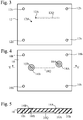
Figs. 1 to 3 , in theflow passage plate 12 of themicrofluidic chip 5, arecess 12Q that forms a flow passage 12P for liquid and acommunication hole 12A communicating with one end of therecess 12Q are formed. Thecommunication hole 12A is aligned with the through-hole 6A of the protectionflat plate 6. A through-hole 12B is formed in theflow passage plate 12. The through-hole 12B is aligned with the through-hole 6B of the protectionflat plate 6. - The
flat plate 11 of themicrofluidic chip 5 is stacked under theflow passage plate 12 to close therecess 12Q to define the flow passage 12P. In theflat plate 11, a communication through-hole 11A communicating with the other end of therecess 12Q, and a through-hole 11B aligned with the through-hole 12B of theflow passage plate 12, are formed. - As shown in
Figs. 1, 2 ,4, and 5 , in theflow passage plate 10 of themicrofluidic chip 4, arecess 10Q that forms aflow passage 10P for liquid, and acommunication hole 10B communicating with one end of therecess 10Q, are formed. Thecommunication hole 10B is aligned with the through-hole 6B of the protectionflat plate 6, the through-hole 12B of theflow passage plate 12, and the through-hole 11B of theflat plate 11. A through-hole 10A is formed inflow passage plate 10. The through-hole 10A is aligned with the communication through-hole 11A of theflat plate 11. - The flat plate 9 of the
microfluidic chip 4 is stacked under theflow passage plate 10 to close therecess 10Q for defining theflow passage 10P. In the flat plate 9, a communication through-hole 9B communicating with the other end of therecess 10Q, and a through-hole 9A aligned with the through-hole 10A of theflow passage plate 10 are formed. - As shown in
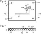
Figs. 1, 2 ,6, and 7 , in theflow passage plate 8 of themicrofluidic chip 3, arecess 8Q that forms aflow passage 8P for liquid, andcommunication holes flow passage 8P, are formed. Thecommunication hole 8A is aligned with the communication through-hole 11A of theflat plate 11, the through-hole 10A of theflow passage plate 10, and the through-hole 9A of the flat plate 9. Thecommunication hole 8B is aligned with the communication through-hole 9B of the flat plate 9. - The
flat plate 7 of themicrofluidic chip 3 is stacked under theflow passage plate 8 to close therecess 8Q for defining theflow passage 8P. In theflat plate 7, a communication through-hole 7C communicating with the other end of therecess 8Q is formed. - In the supporting
flat plate 2, a through-hole 2C aligned with the communication through-hole 7C of theflat plate 7 is formed. The communication through-hole 7C and the through-hole 2C are outlet ports for liquid in the microfluidic device 1. Aliquid suction device 20C (e.g., a tube connected with a suction pump (not shown)) is, for example, connected with the through-hole 2C, respectively. However, the supportingflat plate 2 is not absolutely necessary. - In the above configuration, the liquid supplied from the
injector 19A flows into theflow passage 8P through the through-hole 6A, thecommunication hole 12A, the flow passage 12P, the communication through-hole 11A, the through-hole 9A, and thecommunication hole 8A. The liquid supplied from theinjector 19B flows into theflow passage 8P through the through-hole 6B, the through-hole 12B, the through-hole 11B, thecommunication hole 10B, theflow passage 10P, the communication through-hole 9B, and thecommunication hole 8B. - The two kinds of liquids merging together at the
flow passage 8P are mixed in theflow passage 8P, and the reaction state occurring thereat is observed. In this embodiment, theflow passage plates flat plates 9 and 11, and the protectionflat plate 6 located above theflow passage 8P are made of transparent materials. In addition, as shown inFig. 2 , theflow passage 8P is located at a location that is different from theflow passages 10P and 12P when viewed from above. Thus, the reaction state of the liquids in theflow passage 8P can be easily observed from above by the human eye or using an optical instrument. In addition, since theflow passages flow passages - As shown in
Figs. 1 ,4, and 5 ,annular seals flow passage plate 10 of themicrofluidic chip 4 and surround the through-hole 10A and thecommunication hole 10B, respectively. Theannular seals flow passage plate 10, i.e., the surface that is in contact with theflat plate 11 of themicrofluidic chip 5, and theannular seals flow passage plate 10 and theflat plate 11, so that leakage of liquid between themicrofluidic chips hole 11A to the through-hole 10A is surrounded by theannular seal 14A and leakage therefrom is prevented or reduced, whereas the liquid flowing from the communication through-hole 11B to thecommunication hole 10B is surrounded by theannular seal 14B and leakage therefrom is prevented or reduced. - The elastomer for making the
annular seals annular seals flow passage plate 10. - As shown in
Figs. 1 ,6, and 7 ,annular seals flow passage plate 8 of themicrofluidic chip 3 and surround thecommunication holes annular seals flow passage plate 8, i.e., the surface that is in contact with the flat plate 9 of themicrofluidic chip 4, and theannular seals flow passage plate 8 and the flat plate 9, so that leakage of liquid between themicrofluidic chips hole 9A to thecommunication hole 8A is surrounded by theannular seal 13A and leakage therefrom is prevented or reduced, whereas the liquid flowing from the communication through-hole 9B to thecommunication hole 8B is surrounded by theannular seal 13B and leakage therefrom is prevented or reduced. - The elastomer for making the
annular seals annular seals flow passage plate 8. - In this embodiment, the
flow passage 8P of themicrofluidic chip 3 is formed easily, without using a tube, by combining theflow passage plate 8 in which therecess 8Q forming theflow passage 8P for liquid and thecommunication holes recess 8Q are formed and theflat plate 7 in which the communication through-hole 7C communicating with therecess 8Q is formed. In addition, theflow passage 10P of themicrofluidic chip 4 is formed easily, without using a tube, by combining theflow passage plate 10 in which therecess 10Q forming theflow passage 10P for liquid and thecommunication hole 10B communicating with therecess 10Q are formed and the flat plate 9 in which the communication through-hole 9B communicating with therecess 10Q is formed. Furthermore, the flow passage 12P of themicrofluidic chip 5 is formed easily, without using a tube, by combining theflow passage plate 12 in which therecess 12Q forming the flow passage 12P for liquid and thecommunication hole 12A communicating with therecess 12Q are formed and theflat plate 11 in which the communication through-hole 11A communicating with therecess 12Q is formed. - In this embodiment, the microfluidic device 1 can be formed by stacking multiple
microfluidic chips - By changing the laminated microfluidic chips depending on the application, a microfluidic device appropriate to the application can be formed easily. For example, in the above example, the
microfluidic chip 5 is used for supplying a type of liquid, and themicrofluidic chip 4 is used for passing the liquid and for supplying another kind of liquid, whereas themicrofluidic chip 3 is used for mixing these liquids. However, another microfluidic device may be formed including a microfluidic chip for introducing two kinds of liquids, a macrofluidic chip for mixing these liquids, a microfluidic chip for separating a necessary component from these liquids, and a microfluidic chip for analyzing the separated component. In this case, themicrofluidic chip 3 for mixing liquids may be used for these two examples. - Accordingly, a satisfactory microfluidic device appropriate to the use can be formed by selecting microfluidic chips suitable for processes, even if the type of process using liquids, the order of processes, and the number of processes are changed.
- In the formed microfluidic device, each of the
microfluidic chips flow passage multiple flow passages - In this embodiment, the microfluidic device 1 has a laminated structure including multiple plates stacked one on top of another. In this structure, elements made of elastomer reduce or prevent leakage of liquid from the pathway. Specifically, in the
microfluidic chip 3, theflow passage plate 8 is made of a soft elastomer. Accordingly, it is easy to form therecess 8Q that forms theflow passage 8P, and when the stackedflow passage plate 8 and theflat plate 7 are compressed, theflat plate 8 adheres tightly to theflat plate 7 for reducing or preventing leakage of liquid therebetween. In themicrofluidic chip 4, theflow passage plate 10 is made of a soft elastomer. Accordingly, it is easy to form therecess 10Q that forms theflow passage 10P, and when the stackedflow passage plate 10 and the flat plate 9 are compressed, theflow passage plate 10 adheres tightly to the flat plate 9 for reducing or preventing leakage of liquid therebetween. In themicrofluidic chip 5, theflow passage plate 12 is made of a soft elastomer. Accordingly, it is easy to form therecess 12Q that forms the flow passage 12P, and when the stackedflow passage plate 12 and theflat plate 11 are compressed, theflow passage plate 12 adheres tightly to theflat plate 11 so as to reduce or prevent leakage of liquid therebetween. In addition, when the stackedflow passage plate 12 and the protectionflat plate 6 are compressed, theflow passage plate 12 adheres tightly to the protectionflat plate 6 to reduce or prevent leakage of liquid therebetween. - The
annular seals flow passage plate 8 of themicrofluidic chip 3 are in contact with, and are compressed by, the flat plate 9 of the othermicrofluidic chip 4, and allow the flow of the fluid between themicrofluidic chips annular seals flow passage plate 10 of themicrofluidic chip 4 are in contact with and are compressed by theflat plate 11 of the othermicrofluidic chip 5, and allow the flow of the fluid between themicrofluidic chips - In this embodiment, the
annular seals flow passage plate 8, whereas theannular seals flow passage plate 10. Accordingly, treatment of themicrofluidic chips - In this embodiment, in each
plate holes microfluidic chips multiple pins 16 into the fixing through-holes microfluidic chips microfluidic chips - As described above, in the laminated structure, elements made of elastomer reduce or prevent leakage of liquid from the pathway. The fixing tools, for example, nuts 18 attached to the
pins 16, compress and elastically deform the elastomer elements for enhancing the sealing capability thereof. However, if necessary, the plates may be joined together using an adhesive, a chemical reaction, or a thermal reaction. - Next, the method for producing the microfluidic device 1 according to this embodiment will be described. The following manufacturing method is an example, and the microfluidic device 1 may be manufactured by another method.
- First, the method for producing a mold for manufacturing the
flow passage plate 10 of themicrofluidic chip 4 will be described. Theflow passage plates - As shown in
Fig. 8 , anepoxy resin solution 21 was dropped onto a P-type silicon wafer 20 with crystal orientation <100>, and was made uniform by spin coating. As theepoxy resin solution 21, a negative photoresist manufactured by Nippon Kayaku Co., Ltd. (trade name "SU8 3050") was used. Spin coating was carried out at 2000 rpm for 30 seconds. - Then, in order to dry the solvent of the
epoxy resin solution 21, as shown inFig. 9 , pre-baking was carried out for 25 minutes at a temperature of 95 degrees Celsius by means of aheater 24 to form a driedepoxy resin layer 22. After that, as shown inFig. 10 , amask 26 was placed on theepoxy resin layer 22, and theepoxy resin layer 22 was irradiated with ultraviolet light by the use of a mercury lamp to harden a desired portion of theepoxy resin layer 22. Themask 26 is used to form a part in the mold corresponding to therecess 10Q of theflow passage plate 10, and has the same size and the same shape as therecess 10Q. - Then, in order to complete the polymerization reaction of epoxy resin, baking was carried out for 5 minutes at a temperature of 95 degrees Celsius using the
heater 24 as shown inFig. 11 . After that, the portion that was not in contact with themask 26 and was not hardened was removed by a developer (trade name "SU8 developer") to form a remainingresin protrusion 22a corresponding to therecess 10Q as shown inFig. 12 . Then, thesilicon wafer 20 was cleaned with isopropyl alcohol, resulting in that amold 28 having thesilicon wafer 20 and the remainingresin protrusion 22a was completed. - Then, as shown in
Fig. 13 ,pins 29a, 29b, and 29h were joined to themold 28. The pins 29a and 29b correspond to the through-hole 10A and thecommunication hole 10B of theflow passage plate 10, respectively, whereas thepins 29h correspond to the fixing through-holes 10h of theflow passage plate 10, respectively. - Another
mold 30, havingrecesses recesses annular seals molds molds molds flow passage plate 10 made of the silicone rubber to which the shapes of themolds hole 10A, thecommunication hole 10B, and the fixing through-holes 10h may be formed after molding of theflow passage plate 10. - Furthermore, as shown in
Fig. 14 , the flat plate 9 made of glass in which the through-holes holes 9h were formed was joined to theflow passage plate 10. However, bonding of the flat plate 9 and theflow passage plate 10 is not absolutely necessary. It might be preferable not to join them because it would be easier to clean, wash, or dry theflow passage 10P when removing themicrofluidic chip 4 from thepins 16. - Thus, the
microfluidic chips flat plate 2, themicrofluidic chips flat plate 6 were stacked one on top of another. Next, by insertingmultiple pins 16 through the fixing through-holes flow passage plates annular seals - Although the present invention has been described, the foregoing description is not intended to limit the present invention. Various modifications including one or more deletions, additions, and substitutions of structural elements may be made within the scope of the present invention.
- For example, in the above-described embodiment, the
annular seals flow passage plate 8, whereas theannular seals flow passage plate 10. However, the annular seals may be joined to the flow passage plate using an adhesive, a chemical reaction, or a thermal reaction. - The annular seals may be separable from the flow passage plate.
Fig. 15 shows anannular seal 42 separable from theflow passage plate 40. Theannular seal 42 is located so as to be in contact with the upper surface of theflow passage plate 40, and surrounds ahole 44 of theflow passage plate 40. Theannular seal 42 is located between the lower surface of another microfluidic chip and the upper surface of theflow passage plate 40, and is compressed therebetween to be elastically deformed for preventing or reducing leakage of the fluid to the outside. An annular seal, such as an O-ring or a D-ring, may be used as theannular seal 42. As shown inFig. 16 , arecess 40A that may be used for the seat of theannular seal 42 may be formed on the upper surface of theflow passage plate 40. - In a case in which the annular seals are separable from the flow passage plate, it is unnecessary to form the flow passage plate of an elastomer. For example, it may be made of glass or a transparent resin.
- In the above-described embodiment, in each microfluidic chip, the flow passage plate is located above the flat plate, but the arrangement may be reversed.
- In the above-described embodiment, the annular seals are provided on the flow passage plate of the microfluidic chip. Instead of, or in addition to this, annular seals may be provided on the flat plate of the microfluidic chip. In the above-described embodiment, the annular seals are provided on the plate of the microfluidic chip in which the liquid introduction ports for liquid are formed. Instead of, or in addition to this, annular seals may be provided on the plate in which outlet ports for liquid are formed.
Fig. 17 shows amicrofluidic device 50 according to a variation in which annular seals are located on the upper and lower surfaces of each microfluidic chip, respectively. Themicrofluidic device 50 includesmicrofluidic chips microfluidic chip 51 including aflow passage plate 53 and aflat plate 54, themicrofluidic chip 52 including aflow passage plate 55 and aflat plate 56. Anannular seal 57 is located on the lower surface of theflat plate 54, whereas anannular seal 58 is located on the upper surface of theflow passage plate 53. Anannular seal 59 is located on the lower surface of theflat plate 56, whereas anannular seal 60 is located on the upper surface of theflow passage plate 55. Theannular seals flow passage plate 53 of themicrofluidic chip 51 and theflat plate 56 of themicrofluidic chip 52 so as to be deformed for preventing or reducing leakage of fluid to the outside. In theflow passage plates flat plates - In the above-described embodiment, no annular seals are located between the
flow passage plate 12 of themicrofluidic chip 5 and the protectionflat plate 6, but annular seals may be located therebetween. In the above-described embodiment, no annular seals are located between the supportingflat plate 2 and theflat plate 7 of themicrofluidic chip 3, but annular seals may be located therebetween. - As described above, each annular seal is compressed between plates and reduced in the thickness direction thereof. However, it is likely that the plate is located above an annular seal, and that this fluidic chip cannot be oriented horizontally. For example, such concerns may arise in a case in which there are only one of two annular seals in a layer, or the gap between annular seals in a layer is small. Accordingly, as necessary, preferably, three or more spacers may be placed in the same layer as the annular seals. These spacers have the same height as one another, this height being less than the height of the annular seals in the uncompressed state and being equivalent to the desired height of the annular seal when compressed.
Fig. 18 shows an example of microfluidic device 1 in which spacers 62 are provided. In this example,multiple spacers 62 are arranged in the layer between theflow passage plate 8 and the flat plate 9, andmultiple spacers 62 are also arranged between theflow passage plate 10 and theflat plate 11. In this example, eachspacer 62 is a ring arranged around apin 16, and fourspacers 62 are provided in one layer. However, the spacers do not have to have the shape of ring, and they need not be arranged around thepins 16 if the spacers are arranged at a sufficient distance from each other - Aspects of the present invention are also set out in the following numbered clauses:
- Clause 1. A microfluidic chip comprising:
- a flow passage plate in which a recess forming a flow passage for liquid and a communication hole communicating with the recess are formed;
- a flat plate stacked on or under the flow passage plate to close the recess for defining the flow passage, a communication through-hole communicating with the recess is formed in the flat plate; and
- an annular seal made of an elastomer located on, or formed on, an outer surface of at least one of the flow passage plate and the flat plate, the annular seal surrounding at least one of the communication hole and the communication through-hole.
-
Clause 2. The microfluidic chip according to clause 1, wherein at least one of the flow passage plate and the flat plate is made of the elastomer and formed integrally with the annular seal.
In this case, since the annular seal is integral with at least one of the flow passage plate and the flat plate, treatment of the microfluidic chip is easy, and manufacturing of the microfluidic device is also easy. -
Clause 3. The microfluidic chip according toclause 1 or 2, wherein multiple fixing through-holes are formed in the flow passage plate, and wherein multiple fixing through-holes that are aligned with the multiple fixing through-holes of the flow passage plate, respectively, are formed in the flat plate.
In this case, when the microfluidic device is constructed with multiple microfluidic chips, by inserting the multiple pins into the fixing through-holes of the flow passage plate and the flat plate, multiple microfluidic chips can be easily positioned relative to each other, and the multiple microfluidic chips can be easily integrated by using fixing tools. -
Clause 4. The microfluidic chip according to any one of clauses 1 to 3, wherein at least one of the flow passage plate and the flat plate is transparent.
In this case, the state of liquid in the flow passage can be easily observed by the human eye or by an optical instrument. -
Clause 5. A microfluidic device comprising:- multiple microfluidic chips according to any one of clauses 1 to 4, the microfluidic chips comprising the flow passages of different types, respectively,
- the multiple microfluidic chips stacked one on top of another, such that the communication hole or the communication through-hole of one of the microfluidic chips is aligned with the communication hole or the communication through-hole of a neighboring microfluidic chip.
-
Clause 6. The microfluidic device according toclause 5, wherein the flow passages of the multiple microfluidic chips are located at different positions from each other when viewed from above. - In this case, the state of liquid in multiple flow passages can be easily observed by the human eye or by an optical instrument.
-
- 1, 50: Microfluidic Device
- 2: Supporting Flat Plate
- 2C: Through-Hole
- 3, 4, 5, 51, 52: Microfluidic Chip
- 6: Protection Flat Plate
- 6a, 6b: Through-Hole
- 7, 9, 11, 54, 56: Flat Plate
- 8, 10, 12, 40, 53, 55: Flow Passage Plate
- 2h, 3h, 4h, 5h, 6h, 7h, 8h, 9h, 10h, 11h, 12h: Fixing Through-Hole
- 16: Pin
- 18: Nut 18 (Fixing Tool)
- 8P, 10P, 12P: Flow Passage
- 8Q, 10Q, 12Q: Recess
- 7C, 9B, 11A: Communication Through-Hole
- 8A, 8B, 10B, 12A: Communication Hole
- 9A, 10A, 11B, 12B: Through-Hole
- 13A, 13B, 14A, 14B, 42, 57, 58, 59, 60: Annular Seal
Claims (4)
- A microfluidic chip comprising:a flow passage plate in which a recess forming a flow passage for liquid and a communication hole communicating with the recess are formed;a flat plate stacked on or under the flow passage plate to close the recess for defining the flow passage, a communication through-hole communicating with the recess is formed in the flat plate; andan annular seal made of an elastomer located on, or formed on, an outer surface of at least one of the flow passage plate and the flat plate, the annular seal surrounding at least one of the communication hole and the communication through-hole.
- The microfluidic chip according to claim 1, wherein at least one of the flow passage plate and the flat plate is made of the elastomer and formed integrally with the annular seal.
- The microfluidic chip according to claim 1 or 2, wherein multiple fixing through-holes are formed in the flow passage plate, and wherein multiple fixing through-holes that are aligned with the multiple fixing through-holes of the flow passage plate, respectively, are formed in the flat plate.
- A microfluidic device comprising:multiple microfluidic chips according to any one of claims 1 to 3, the microfluidic chips comprising the flow passages of different types, respectively,the multiple microfluidic chips stacked one on top of another, such that the communication hole or the communication through-hole of one of the microfluidic chips is aligned with the communication hole or the communication through-hole of a neighboring microfluidic chip.
Applications Claiming Priority (2)
| Application Number | Priority Date | Filing Date | Title |
|---|---|---|---|
| JP2017217170 | 2017-11-10 | ||
| PCT/JP2018/034615 WO2019092989A1 (en) | 2017-11-10 | 2018-09-19 | Microfluidic chip and microfluidic device |
Publications (2)
| Publication Number | Publication Date |
|---|---|
| EP3708531A1 true EP3708531A1 (en) | 2020-09-16 |
| EP3708531A4 EP3708531A4 (en) | 2020-09-23 |
Family
ID=66438781
Family Applications (1)
| Application Number | Title | Priority Date | Filing Date |
|---|---|---|---|
| EP18876943.4A Pending EP3708531A4 (en) | 2017-11-10 | 2018-09-19 | Microfluidic chip and microfluidic device |
Country Status (5)
| Country | Link |
|---|---|
| US (1) | US11478790B2 (en) |
| EP (1) | EP3708531A4 (en) |
| JP (1) | JPWO2019092989A1 (en) |
| CN (1) | CN110678414A (en) |
| WO (1) | WO2019092989A1 (en) |
Families Citing this family (3)
| Publication number | Priority date | Publication date | Assignee | Title |
|---|---|---|---|---|
| CN113454437B (en) * | 2019-02-27 | 2024-03-15 | 京瓷株式会社 | Particle separation device and particle separation measuring device |
| WO2022147426A1 (en) * | 2020-12-28 | 2022-07-07 | The Trustees Of The University Of Pennsylvania | Microfluidic platforms for large scale nanoparticle formulations |
| GB202118922D0 (en) * | 2021-12-23 | 2022-02-09 | Osler Diagnostics Ltd | Liquid handling device |
Family Cites Families (21)
| Publication number | Priority date | Publication date | Assignee | Title |
|---|---|---|---|---|
| KR100865105B1 (en) * | 1999-06-28 | 2008-10-24 | 캘리포니아 인스티튜트 오브 테크놀로지 | Microfabricated elastomeric valve and pump systems |
| DE10106996C2 (en) | 2001-02-15 | 2003-04-24 | Merck Patent Gmbh | Device for connecting micro components |
| DE10155010A1 (en) | 2001-11-06 | 2003-05-15 | Cpc Cellular Process Chemistry | Microreactor system |
| WO2004034028A2 (en) | 2002-10-09 | 2004-04-22 | The Board Of Trustees Of The University Of Illinois | Microfluidic systems and components |
| EP1730489B1 (en) * | 2004-01-25 | 2020-03-04 | Fluidigm Corporation | Crystal forming devices and systems and methods for making and using the same |
| GB0421529D0 (en) * | 2004-09-28 | 2004-10-27 | Landegren Gene Technology Ab | Microfluidic structure |
| US7297285B2 (en) * | 2005-08-05 | 2007-11-20 | Roger Chang | Manufacturing process of emboss type flexible or rigid printed circuit board |
| US20070048189A1 (en) * | 2005-08-26 | 2007-03-01 | Applera Corporation | Fluid processing device, system, kit, and method |
| JP2007092904A (en) * | 2005-09-29 | 2007-04-12 | Nichias Corp | Sheet gasket and its manufacturing method |
| JP2007147456A (en) | 2005-11-28 | 2007-06-14 | Seiko Epson Corp | Micro-fluid system, specimen analyzer, and method for detecting or measuring target substance |
| JP5104316B2 (en) * | 2006-01-12 | 2012-12-19 | 住友ベークライト株式会社 | Passive one-way valve and microfluidic device |
| US20080038738A1 (en) * | 2006-05-10 | 2008-02-14 | The Board Of Regents Of The University Of Texas System | Detecting tumor biomarker in oral cancer |
| JP5055617B2 (en) | 2007-05-25 | 2012-10-24 | 地方独立行政法人 東京都立産業技術研究センター | Dispensing device |
| EP2265960A2 (en) | 2008-04-25 | 2010-12-29 | Plexigen, Inc. | Biochips and related automated analyzers and methods |
| JP5399885B2 (en) | 2009-12-25 | 2014-01-29 | 株式会社朝日ラバー | Biochip substrate manufacturing method |
| JP5649930B2 (en) | 2010-11-29 | 2015-01-07 | Udトラックス株式会社 | gasket |
| US20140363838A1 (en) * | 2013-06-11 | 2014-12-11 | William Marsh Rice University | Microperfusion imaging platform |
| JP2013208619A (en) | 2013-06-21 | 2013-10-10 | Nisso Engineering Co Ltd | Microreactor |
| WO2015025424A1 (en) * | 2013-08-23 | 2015-02-26 | 株式会社朝日Fr研究所 | Microchemical chip and reaction device |
| JP6272023B2 (en) | 2013-12-26 | 2018-01-31 | 高砂電気工業株式会社 | Microfluidic chip device |
| WO2016098722A1 (en) | 2014-12-15 | 2016-06-23 | 日本電気株式会社 | Microchip, liquid transfer method and microchip controller |
-
2018
- 2018-09-19 EP EP18876943.4A patent/EP3708531A4/en active Pending
- 2018-09-19 WO PCT/JP2018/034615 patent/WO2019092989A1/en unknown
- 2018-09-19 JP JP2019551902A patent/JPWO2019092989A1/en active Pending
- 2018-09-19 CN CN201880034720.6A patent/CN110678414A/en active Pending
- 2018-09-19 US US16/609,258 patent/US11478790B2/en active Active
Also Published As
| Publication number | Publication date |
|---|---|
| US11478790B2 (en) | 2022-10-25 |
| JPWO2019092989A1 (en) | 2020-10-01 |
| CN110678414A (en) | 2020-01-10 |
| WO2019092989A1 (en) | 2019-05-16 |
| EP3708531A4 (en) | 2020-09-23 |
| US20200061614A1 (en) | 2020-02-27 |
Similar Documents
| Publication | Publication Date | Title |
|---|---|---|
| US11478790B2 (en) | Microfluidic chip and microfluidic device | |
| US9341284B2 (en) | Microfluidic devices with mechanically-sealed diaphragm valves | |
| US7060227B2 (en) | Microfluidic devices with raised walls | |
| EP1545780B1 (en) | Modular microfluidic system | |
| AU2005231431B2 (en) | Microfluidic connections | |
| US20020100714A1 (en) | Microfluidic devices | |
| US8747777B2 (en) | Microfluidic apparatus including microfluidic device | |
| EP3693453B1 (en) | Cell capturing device | |
| Chen et al. | Fit-to-Flow (F2F) interconnects: Universal reversible adhesive-free microfluidic adaptors for lab-on-a-chip systems | |
| CN107413401A (en) | Mixed type flat surface optofluidic integrates | |
| KR20080090410A (en) | Fine line bonding and/or sealing system and method | |
| CN109107623B (en) | Micro-fluidic chip and preparation method thereof | |
| WO2002063288A1 (en) | Microfluidic devices | |
| EP1925364A1 (en) | Multiple microfluidic connector | |
| Sabourin et al. | Interconnection blocks: a method for providing reusable, rapid, multiple, aligned and planar microfluidic interconnections | |
| CN111295591B (en) | microchip | |
| WO2015090339A1 (en) | Fluidic microsystem and method of manufacturing thereof | |
| KR101486413B1 (en) | Microfluidic Chip Using Micro-post And Fabricating Method Thereof | |
| Wagler et al. | General-purpose, parallel and reversible microfluidic interconnects | |
| US8087310B2 (en) | Interconnect for MEMS device including a viscoelastic septum | |
| CN108311177B (en) | Manufacturing method of 3D PDMS micro-fluidic chip alignment assembly structure | |
| EP3878940A1 (en) | Cell culturing chip and production method therefor | |
| CN216756490U (en) | Clamp and microfluidic chip device thereof | |
| US11471883B2 (en) | Fluid chip, fluid device, and method for manufacturing same | |
| Gray | Fluidic Interconnects for Microfluidics: Chip to Chip and World to Chip |
Legal Events
| Date | Code | Title | Description |
|---|---|---|---|
| STAA | Information on the status of an ep patent application or granted ep patent |
Free format text: STATUS: THE INTERNATIONAL PUBLICATION HAS BEEN MADE |
|
| PUAI | Public reference made under article 153(3) epc to a published international application that has entered the european phase |
Free format text: ORIGINAL CODE: 0009012 |
|
| STAA | Information on the status of an ep patent application or granted ep patent |
Free format text: STATUS: REQUEST FOR EXAMINATION WAS MADE |
|
| 17P | Request for examination filed |
Effective date: 20191025 |
|
| AK | Designated contracting states |
Kind code of ref document: A1 Designated state(s): AL AT BE BG CH CY CZ DE DK EE ES FI FR GB GR HR HU IE IS IT LI LT LU LV MC MK MT NL NO PL PT RO RS SE SI SK SM TR |
|
| AX | Request for extension of the european patent |
Extension state: BA ME |
|
| A4 | Supplementary search report drawn up and despatched |
Effective date: 20200826 |
|
| RIC1 | Information provided on ipc code assigned before grant |
Ipc: B81B 1/00 20060101AFI20200820BHEP Ipc: B01L 3/00 20060101ALI20200820BHEP Ipc: G01N 37/00 20060101ALI20200820BHEP |
|
| DAV | Request for validation of the european patent (deleted) | ||
| DAX | Request for extension of the european patent (deleted) | ||
| STAA | Information on the status of an ep patent application or granted ep patent |
Free format text: STATUS: EXAMINATION IS IN PROGRESS |
|
| 17Q | First examination report despatched |
Effective date: 20210923 |