EP3707894B1 - Method and apparatus for performing processing in a camera - Google Patents
Method and apparatus for performing processing in a camera Download PDFInfo
- Publication number
- EP3707894B1 EP3707894B1 EP18876707.3A EP18876707A EP3707894B1 EP 3707894 B1 EP3707894 B1 EP 3707894B1 EP 18876707 A EP18876707 A EP 18876707A EP 3707894 B1 EP3707894 B1 EP 3707894B1
- Authority
- EP
- European Patent Office
- Prior art keywords
- component
- decontaminated
- values
- processor
- visible component
- Prior art date
- Legal status (The legal status is an assumption and is not a legal conclusion. Google has not performed a legal analysis and makes no representation as to the accuracy of the status listed.)
- Active
Links
Images




Classifications
-
- H—ELECTRICITY
- H04—ELECTRIC COMMUNICATION TECHNIQUE
- H04N—PICTORIAL COMMUNICATION, e.g. TELEVISION
- H04N23/00—Cameras or camera modules comprising electronic image sensors; Control thereof
- H04N23/80—Camera processing pipelines; Components thereof
- H04N23/81—Camera processing pipelines; Components thereof for suppressing or minimising disturbance in the image signal generation
-
- H—ELECTRICITY
- H04—ELECTRIC COMMUNICATION TECHNIQUE
- H04N—PICTORIAL COMMUNICATION, e.g. TELEVISION
- H04N5/00—Details of television systems
- H04N5/222—Studio circuitry; Studio devices; Studio equipment
- H04N5/262—Studio circuits, e.g. for mixing, switching-over, change of character of image, other special effects ; Cameras specially adapted for the electronic generation of special effects
- H04N5/265—Mixing
-
- G—PHYSICS
- G06—COMPUTING OR CALCULATING; COUNTING
- G06T—IMAGE DATA PROCESSING OR GENERATION, IN GENERAL
- G06T3/00—Geometric image transformations in the plane of the image
- G06T3/40—Scaling of whole images or parts thereof, e.g. expanding or contracting
- G06T3/4007—Scaling of whole images or parts thereof, e.g. expanding or contracting based on interpolation, e.g. bilinear interpolation
-
- H—ELECTRICITY
- H04—ELECTRIC COMMUNICATION TECHNIQUE
- H04N—PICTORIAL COMMUNICATION, e.g. TELEVISION
- H04N23/00—Cameras or camera modules comprising electronic image sensors; Control thereof
- H04N23/10—Cameras or camera modules comprising electronic image sensors; Control thereof for generating image signals from different wavelengths
- H04N23/11—Cameras or camera modules comprising electronic image sensors; Control thereof for generating image signals from different wavelengths for generating image signals from visible and infrared light wavelengths
-
- H—ELECTRICITY
- H04—ELECTRIC COMMUNICATION TECHNIQUE
- H04N—PICTORIAL COMMUNICATION, e.g. TELEVISION
- H04N23/00—Cameras or camera modules comprising electronic image sensors; Control thereof
- H04N23/80—Camera processing pipelines; Components thereof
-
- H—ELECTRICITY
- H04—ELECTRIC COMMUNICATION TECHNIQUE
- H04N—PICTORIAL COMMUNICATION, e.g. TELEVISION
- H04N23/00—Cameras or camera modules comprising electronic image sensors; Control thereof
- H04N23/80—Camera processing pipelines; Components thereof
- H04N23/84—Camera processing pipelines; Components thereof for processing colour signals
- H04N23/843—Demosaicing, e.g. interpolating colour pixel values
-
- H—ELECTRICITY
- H04—ELECTRIC COMMUNICATION TECHNIQUE
- H04N—PICTORIAL COMMUNICATION, e.g. TELEVISION
- H04N25/00—Circuitry of solid-state image sensors [SSIS]; Control thereof
- H04N25/10—Circuitry of solid-state image sensors [SSIS]; Control thereof for transforming different wavelengths into image signals
- H04N25/11—Arrangement of colour filter arrays [CFA]; Filter mosaics
- H04N25/13—Arrangement of colour filter arrays [CFA]; Filter mosaics characterised by the spectral characteristics of the filter elements
- H04N25/131—Arrangement of colour filter arrays [CFA]; Filter mosaics characterised by the spectral characteristics of the filter elements including elements passing infrared wavelengths
Definitions
- an IR filter and sensor In order to capture infrared (IR) images with a camera, an IR filter and sensor is often implemented along with a visible light (red/green/blue "RGB”) filter and sensor that captures visible light images.
- RGB visible light
- the colors resident in the visible image can be contaminated by the IR energy passing through the IR band of the dual band filter, since RGB pixels also have a spectral response in the IR band. Additionally, the IR image can be contaminated by the visible light energy in a similar manner.
- conventional techniques for acquiring a quality RGB image employ a unique image signal processor (ISP), since the pattern of a pixel array on an RGBIR sensor is different than that of a conventional RGB sensor, which produces a conventional RGB "Bayer" pattern.
- ISP image signal processor
- RGBIR sensor some pixels of a conventional Bayer pattern are replaced by IR pixels.
- a conventional ISP is not able to perform conventional processing on the resulting image that it receives from an RGBIR sensor.
- a method according to claim 1 for receiving and processing an image that includes a visible light (red/green/blue "RGB") component and an infrared (IR) component.
- the method allows a conventional image signal processor (ISP) to perform conventional processing an RGBIR signal with a decontamination function being performed on the signal as well as an interpolation (e.g., red, green, blue light interpolation) being performed on the signal.
- ISP image signal processor
- the contamination in the signal can be due to a number of factors.
- some contamination in a received signal may be due to spectral crosstalk which occurs because of imperfect color filters passing through some amount of unwanted light of the colors being filtered out.
- Optical spatial crosstalk contamination is due to color filters being located at some distance from an image pixel surface due to metal and insulation layers. The light coming at angles other than orthogonal passes through a filter and can partially be absorbed by the adjacent pixel being generated rather than one below. Depending on the f-number of the lens, this portion of the light absorbed by a neighboring pixel can vary significantly and can be big enough for low f-numbers.
- Micro-lenses located on the top of color filters can reduce this component of crosstalk significantly when appropriate form of micro-lenses and optimum position of them are chosen.
- Electrical crosstalk contamination results from photo-generated carriers having the possibility to move to neighboring charge accumulation sites. Electrical crosstalk occurs in both monochrome and color image sensors. The quantity of the carriers that can be accumulated by the neighboring pixel and the corresponding crosstalk depends on the pixel structure, collection area, and distribution of sensitivity inside a pixel. Accordingly, infrared light can contaminate the visible component of a received RGBIR image, and visible light can contaminate the infrared component of the received RGBIR image.
- a method of performing processing in an image capturing device includes receiving an image by the image capturing device that includes an infrared component and a visible component.
- a decontamination is performed to generate a decontaminated infrared component and a decontaminated visible component.
- An interpolation is performed on the decontaminated visible component to generate an interpolated visible component, and the decontaminated infrared component and the decontaminated interpolated visible component are provided to an image signal processor (ISP) for further processing.
- An image capturing device is disclosed, The image capturing device includes a camera module, a processor operatively coupled to the camera module, and an image signal processor (ISP) operatively coupled with the processor.
- the camera module receives an image that includes an infrared component and a visible component and forwards the received image to the processor.
- the processor performs a decontamination to generate a decontaminated infrared component and a decontaminated visible component.
- the processor performs an interpolation on the decontaminated visible component to generate an interpolated visible component, and forwards the decontaminated infrared component and the decontaminated interpolated visible component to the ISP for further processing.
- a non-transitory computer readable medium having instructions recorded thereon, that when executed by a computing device, cause the computing device to perform operations is disclosed.
- the operations include receiving an image that includes an infrared component and a visible component.
- a decontamination is performed to generate a decontaminated infrared component and a decontaminated visible component.
- FIG. 1 is a block diagram of an example system 100 in which one or more disclosed embodiments may be implemented.
- the example system 100 includes an image capturing device, (e.g., camera), 110 that includes at least a lens 123 for capturing an image.
- an image capturing device e.g., camera
- the image shown in Figure 1 is a person.
- the image that is captured by the lens 123 includes both visible (RGB) light and IR light. It should be noted that additional types of light can be captured by the lens 123, but for purposes of example, visible and IR are discussed herein.
- Figure 2A is a block diagram of one of the example devices 110 depicted in Figure 1 in which one or more features of the disclosure can be implemented. More detail regarding the implementation of a method of seam finding as it relates to Figure 2 is described in further detail below.
- the device 110 has been described as an image capturing device, (e.g., camera), it is noted that the device 110 can include, for example, a computer, a gaming device, a handheld device, a set-top box, a television, a mobile phone, or a tablet computer.
- the example device 110 is described as an image capturing device 110, which for example is a camera.
- the device 110 includes a processor 102, a memory 104, a storage 106, one or more input devices 108, a camera module 111, and one or more output devices 119.
- the device 110 can also optionally include an input driver 112 and an output driver 114. It is understood that the device 110 can include additional components not shown in Figure 2A .
- the camera module 111 includes the lens 123 described above, a filter 124, and a sensor 125.
- the filter 124 and sensor 125 are a RGBIR filter/sensor pair that perform filtering for the RGB and IR light bands and generation of an RGBIR pattern, described in more detail below.
- the processor 102 includes a central processing unit (CPU), a graphics processing unit (GPU), a CPU and GPU located on the same die, or one or more processor cores, wherein each processor core can be a CPU or a GPU.
- the memory 104 is be located on the same die as the processor 102, or is located separately from the processor 102.
- the memory 104 includes a volatile or non-volatile memory, for example, random access memory (RAM), dynamic RAM, or a cache.
- a conventional image signal processor (ISP) can be included in the processor 102 to perform RGBIR/Bayer image signal processing described in more detail below.
- the ISP can be included in the APD 116 or as a separate processing unit (not shown).
- the storage 106 includes a fixed or removable storage, for example, a hard disk drive, a solid state drive, an optical disk, or a flash drive.
- the input devices 108 include, without limitation, a keyboard, a keypad, a touch screen, a touch pad, a detector, a microphone, an accelerometer, a gyroscope, a biometric scanner, or a network connection (e.g., a wireless local area network card for transmission and/or reception of wireless IEEE 802 signals).
- the output devices 119 include, without limitation, a display, a speaker, a printer, a haptic feedback device, one or more lights, an antenna, or a network connection (e.g., a wireless local area network card for transmission and/or reception of wireless IEEE 802 signals).
- a network connection e.g., a wireless local area network card for transmission and/or reception of wireless IEEE 802 signals.
- the input driver 112 communicates with the processor 102 the input devices 108, and the lens 111, and permits the processor 102 to receive input from the input devices 108 and the lens 111.
- the output driver 114 communicates with the processor 102 and the output devices 110, and permits the processor 102 to send output to the output devices 119. It is noted that the input driver 112 and the output driver 114 are optional components, and that the device 110 will operate in the same manner if the input driver 112 and the output driver 114 are not present.
- the output driver 114 includes an accelerated processing device ("APD") 116 which is coupled to a display device 118.
- APD accelerated processing device
- the APD is configured to accept compute commands and graphics rendering commands from processor 102, to process those compute and graphics rendering commands, and to provide pixel output to display device 118 for display.
- the APD 116 includes one or more parallel processing units configured to perform computations in accordance with a single-instruction-multiple-data (“SIMD") paradigm.
- SIMD single-instruction-multiple-data
- any processing system that performs processing tasks in accordance with a SIMD paradigm may be configured to perform the functionality described herein.
- computing systems that do not perform processing tasks in accordance with a SIMD paradigm performs the functionality described herein.
- the image signal processing described herein can also be performed by the APD 116.
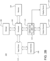
- Figure 2B is a block diagram of an example system 210 in which one or more features of the disclosure can be implemented.
- the system 210 includes substantially similar components to the device 110, except for the camera module 111.
- the system 210 can include, for example, a computer, a gaming device, a handheld device, a set-top box, a television, a mobile phone, or a tablet computer.
- the system 210 can be in communication with the device 110 depicted in Figure 1 and can provide control programming to the device 110 and receive data from the device 110.
- FIG. 3 is a block diagram of the device 110 and system 210, illustrating additional details related to execution of processing tasks on the APD 116. For example, the calibration, decontamination and interpolation operations described below can be performed where appropriate utilizing the parallel SIMD paradigm described herein.
- the processor 102 maintains, in system memory 104, one or more control logic modules for execution by the processor 102.
- the control logic modules include an operating system 120, a kernel mode driver 122, and applications 126. These control logic modules control various features of the operation of the processor 102 and the APD 116.
- the operating system 120 directly communicates with hardware and provides an interface to the hardware for other software executing on the processor 102.
- the kernel mode driver 122 controls operation of the APD 116 by, for example, providing an application programming interface ("API") to software (e.g., applications 126) executing on the processor 102 to access various functionality of the APD 116.
- the kernel mode driver 122 also includes a just-in-time compiler that compiles programs for execution by processing components (such as the SIMD units 138 discussed in further detail below) of the APD 116.
- the APD 116 executes commands and programs for selected functions, such as graphics operations and non-graphics operations that may be suited for parallel processing.
- the APD 116 can be used for executing graphics pipeline operations such as pixel operations, geometric computations, and rendering an image to display device 118 based on commands received from the processor 102.
- the APD 116 also executes compute processing operations that are not directly related to graphics operations, such as operations related to video, physics simulations, computational fluid dynamics, or other tasks, based on commands received from the processor 102.
- the APD 116 includes compute units 132 that include one or more SIMD units 138 that are configured to perform operations at the request of the processor 102 in a parallel manner according to a SIMD paradigm.
- the SIMD paradigm is one in which multiple processing elements share a single program control flow unit and program counter and thus execute the same program but are able to execute that program with different data.
- each SIMD unit 138 includes sixteen lanes, where each lane executes the same instruction at the same time as the other lanes in the SIMD unit 138 but can execute that instruction with different data. Lanes can be switched off with predication if not all lanes need to execute a given instruction. Predication can also be used to execute programs with divergent control flow. More specifically, for programs with conditional branches or other instructions where control flow is based on calculations performed by an individual lane, predication of lanes corresponding to control flow paths not currently being executed, and serial execution of different control flow paths allows for arbitrary control flow.
- the basic unit of execution in compute units 132 is a work-item.
- Each work-item represents a single instantiation of a program that is to be executed in parallel in a particular lane.
- Work-items can be executed simultaneously as a "wavefront" on a single SIMD processing unit 138.
- One or more wavefronts are included in a "work group," which includes a collection of work-items designated to execute the same program.
- a work group can be executed by executing each of the wavefronts that make up the work group.
- the wavefronts are executed sequentially on a single SIMD unit 138 or partially or fully in parallel on different SIMD units 138.
- Wavefronts can be thought of as the largest collection of work-items that can be executed simultaneously on a single SIMD unit 138.
- commands received from the processor 102 indicate that a particular program is to be parallelized to such a degree that the program cannot execute on a single SIMD unit 138 simultaneously, then that program is broken up into wavefronts which are parallelized on two or more SIMD units 138 or serialized on the same SIMD unit 138 (or both parallelized and serialized as needed).
- a scheduler 136 is configured to perform operations related to scheduling various wavefronts on different compute units 132 and SIMD units 138.
- the parallelism afforded by the compute units 132 is suitable for graphics related operations such as pixel value calculations, vertex transformations, and other graphics operations.
- a graphics pipeline 134 which accepts graphics processing commands from the processor 102, provides computation tasks to the compute units 132 for execution in parallel.
- the compute units 132 are also used to perform computation tasks not related to graphics or not performed as part of the "normal" operation of a graphics pipeline 134 (e.g., custom operations performed to supplement processing performed for operation of the graphics pipeline 134).
- An application 126 or other software executing on the processor 102 transmits programs that define such computation tasks to the APD 116 for execution.
- the method described herein (e.g., the decontamination and the interpolation described below), can be performed by sending the instructions to the compute units 132 of the APD 116 for execution.
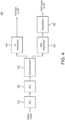
- FIG. 4 is a flow diagram of an example method 400 for performing processing in a camera.
- a captured image that includes an RGB and IR component (e.g., captured by camera 110) undergoes black level correction (BLC).
- BLC is a conventional process for removing the black level in the input RGBIR image.
- DPC defect pixel correction
- the DPC operation is a conventional operation where a pixel is compared to surrounding pixels, and if the differences between the pixel and the surrounding pixels exceeds a pre-defined threshold or is below another pre-defined threshold, the pixel is replaced, (e.g., with a pixel that is derived from the average values of the surrounding pixels).
- These conventional operations, (e.g., steps 410 and 420), can be performed by the processor 102 or APD 116 described above.
- Decontamination is then performed (step 430) to remove IR light energy from the visible component and RGB light energy from the infrared component.
- the decontamination operation can be performed by the processor 102 or the APD 116.
- the RGBIR image is transferred into memory, (e.g., memory 104).
- the image is then fed back into the processor, (e.g., processor 102 or APD 116), to be decontaminated for the generation of a still image or video for output.
- the decontaminated image includes a separate visible component and an infrared component.
- the decontamination may be modeled in accordance with the following.
- a calibration process can be performed prior to decontamination to determine a contamination factor that defines how much contamination exists in the received signal, (e.g., the contamination matrix A) based upon non-contaminated values.
- This calibration can be performed by generating one uniform test chart, which is a diffusor backlighted by narrow spectrum band light, (Red, Green, Blue or NIR), and capturing a series of raw images with an RGBIR camera, (e.g., image device 110), on the test chart.
- the raw data generated can be used to calculate the contamination factor for each channel, (e.g., R/G/B/IR), to form the matrix A for each pixel position.
- matrix A is the contamination matrix representing the contamination that is applied to the ideal non-contaminated values to arrive at the observed, contaminated signal levels.
- the values of the components in the matrix can be utilized to remove unwanted contamination, (e.g., RGB or IR energy), from the image to generate the decontaminated visible component and infrared component.
- unwanted contamination e.g., RGB or IR energy
- the decontamination step removes a portion of the energy from the decontaminated image, potentially producing some level of a distorted component
- an adjustment can be performed on the resultant components to account for the energy loss. Therefore, once decontaminated in step 430, an IR adjustment is performed in step 440, as well as an RGB adjustment in step 450.
- the IR adjustment (step 440) is performed on the infrared component.
- the adjustment operations, e.g., steps 440 and 450
- an example 8 bit pixel has a value between 0-255.
- the value will usually approach the upper boundary 255, therefore the energy removal by decontamination in such an area results in a highlight contour, (i.e., discontinuity), pattern.
- the observed IR image is compared against a pre-defined threshold, and if the value is greater than the pre-defined threshold, the strength of decontamination is degraded gradually towards the upper boundary 255 so that the discontinuity will not happen. That is, less decontamination may be performed, or not performed at all.
- the threshold can be increased or decreased, (e.g., by a programmer), as desired according to the visual effect being rendered.
- the decontaminated RGB component is adjusted, (e.g., by the processor 102 or the APD 116). That is, when removing the IR energy from the RGBIR image, dark areas are left in the image. If the image includes a large percentage of IR energy that is removed, this can lead to a very noticeable difference in the RGB component where the dark regions occur. Accordingly, the output decontaminated RGB image is compared against a pre-defined threshold, and if the value is less than the pre-defined threshold, a portion of the non-decontaminated RGB image is added back to the output RGB component to degrade the strength of decontamination in that portion. This threshold can also be increased or decreased according to the visual effect being rendered.
- FIG. 5A shows an example RGBIR pattern 500. As shown in pattern 500, there are four 2 x 2 RGBIR patterns, each group including a group of B, G, IR, R components. One group is shown in the top left quadrant, one group in the top right quadrant, one group in the bottom left quadrant, and one group in the bottom right quadrant.
- each IR component removed during decontamination is replaced with a G component. Therefore, Figure 5B shows an example interpolated Bayer pattern 500B with IR contamination removed.
- the decontaminated and adjusted IR Image, and the decontaminated, adjusted and interpolated RGB image are both then provided to the conventional ISP for further conventional processing.
- an example 2 x 2 Bayer pattern can include four possible layouts, "RGGB”, “BGGR”, “GRBG” or "GBRG”.
- the example BGGR layout depicted in Figure 5B is one example layout interpolating from that in Figure 5A .
- processors include, by way of example, a general purpose processor, a special purpose processor, a conventional processor, a digital signal processor (DSP), a plurality of microprocessors, graphics processor, one or more microprocessors in association with a DSP core, a controller, a microcontroller, Application Specific Integrated Circuits (ASICs), Field Programmable Gate Arrays (FPGAs) circuits, any other type of integrated circuit (IC), and/or a state machine.
- DSP digital signal processor
- ASICs Application Specific Integrated Circuits
- FPGAs Field Programmable Gate Arrays
- Such processors can be manufactured by configuring a manufacturing process using the results of processed hardware description language (HDL) instructions and other intermediary data including netlists (such instructions capable of being stored on a computer readable media).
- HDL hardware description language
- results of such processing can be maskworks that are then used in a semiconductor manufacturing process to manufacture a processor which implements aspects of the embodiments.
- the above methods can be implemented either in a hardware implementation of a system on chip (SoC), or in the programming of a GPU to compute normal RGB and IR images.
- SoC system on chip
- non-transitory computer-readable storage mediums include a read only memory (ROM), a random access memory (RAM), a register, cache memory, semiconductor memory devices, magnetic media such as internal hard disks and removable disks, magneto-optical media, and optical media such as CD-ROM disks, and digital versatile disks (DVDs).
- ROM read only memory
- RAM random access memory
- register cache memory
- semiconductor memory devices magnetic media such as internal hard disks and removable disks, magneto-optical media, and optical media such as CD-ROM disks, and digital versatile disks (DVDs).
Landscapes
- Engineering & Computer Science (AREA)
- Multimedia (AREA)
- Signal Processing (AREA)
- Physics & Mathematics (AREA)
- Spectroscopy & Molecular Physics (AREA)
- General Physics & Mathematics (AREA)
- Theoretical Computer Science (AREA)
- Image Processing (AREA)
- Color Television Image Signal Generators (AREA)
- Studio Devices (AREA)
Description
- This application claims priority to
Chinese Patent Application No. 201711090962.0, filed November 8, 2017 U.S. Patent Application No. 15/816,537 filed November 17, 2017 - In order to capture infrared (IR) images with a camera, an IR filter and sensor is often implemented along with a visible light (red/green/blue "RGB") filter and sensor that captures visible light images. The use of a dual band RGBIR filter allows a single camera to be utilized to capture both visible light images and IR images. By using a single camera, size and cost can be saved, as well as avoiding the need to do a geometry calibration that is required when two cameras are utilized.
- However, the colors resident in the visible image can be contaminated by the IR energy passing through the IR band of the dual band filter, since RGB pixels also have a spectral response in the IR band. Additionally, the IR image can be contaminated by the visible light energy in a similar manner.
- Accordingly, in a camera that has a dual band RGBIR filter, conventional techniques for acquiring a quality RGB image employ a unique image signal processor (ISP), since the pattern of a pixel array on an RGBIR sensor is different than that of a conventional RGB sensor, which produces a conventional RGB "Bayer" pattern. Using an RGBIR sensor, some pixels of a conventional Bayer pattern are replaced by IR pixels. A conventional ISP is not able to perform conventional processing on the resulting image that it receives from an RGBIR sensor.
US 2015/062347 A1 and Tang Huixuan et al: "High Resolution Photography with an RGB-Infrared Camera", published in proceedings of 2015 IEEE International Conference on Computational Photography (ICCP) disclose and RGB-IR image sensor with image signal decontamination based on cross-talk and providing RGB and IR images for further processing. - A more detailed understanding can be had from the following description, given by way of example in conjunction with the accompanying drawings.
-
Figure 1 is a block diagram of an example system in which one or more disclosed embodiments may be implemented; -
Figure 2A is a block diagram of an example device depicted inFigure 1 in which one or more features of the disclosure can be implemented; -
Figure 2B is a block diagram of an example system in which one or more features of the disclosure can be implemented; -
Figure 3 is a block diagram of the example device ofFigure 2A and example system ofFigure 2B , illustrating additional detail; -
Figure 4 is a flow diagram of an example method for performing processing in a camera; -
Figure 5A shows an example RGBIR pattern including IR contamination; and -
Figure 5B shows an example interpolated Bayer pattern with IR contamination removed. - Although a more detailed description follows, briefly a method according to claim 1, an apparatus according to claim 8, and a computer program according to claim 15 is described herein for receiving and processing an image that includes a visible light (red/green/blue "RGB") component and an infrared (IR) component. The method allows a conventional image signal processor (ISP) to perform conventional processing an RGBIR signal with a decontamination function being performed on the signal as well as an interpolation (e.g., red, green, blue light interpolation) being performed on the signal. The contamination in the signal can be due to a number of factors.
- For example, some contamination in a received signal may be due to spectral crosstalk which occurs because of imperfect color filters passing through some amount of unwanted light of the colors being filtered out. Optical spatial crosstalk contamination is due to color filters being located at some distance from an image pixel surface due to metal and insulation layers. The light coming at angles other than orthogonal passes through a filter and can partially be absorbed by the adjacent pixel being generated rather than one below. Depending on the f-number of the lens, this portion of the light absorbed by a neighboring pixel can vary significantly and can be big enough for low f-numbers. Micro-lenses located on the top of color filters can reduce this component of crosstalk significantly when appropriate form of micro-lenses and optimum position of them are chosen. Electrical crosstalk contamination results from photo-generated carriers having the possibility to move to neighboring charge accumulation sites. Electrical crosstalk occurs in both monochrome and color image sensors. The quantity of the carriers that can be accumulated by the neighboring pixel and the corresponding crosstalk depends on the pixel structure, collection area, and distribution of sensitivity inside a pixel. Accordingly, infrared light can contaminate the visible component of a received RGBIR image, and visible light can contaminate the infrared component of the received RGBIR image.
- A method of performing processing in an image capturing device is disclosed. The method includes receiving an image by the image capturing device that includes an infrared component and a visible component. A decontamination is performed to generate a decontaminated infrared component and a decontaminated visible component. An interpolation is performed on the decontaminated visible component to generate an interpolated visible component, and the decontaminated infrared component and the decontaminated interpolated visible component are provided to an image signal processor (ISP) for further processing. An image capturing device is disclosed, The image capturing device includes a camera module, a processor operatively coupled to the camera module, and an image signal processor (ISP) operatively coupled with the processor. The camera module receives an image that includes an infrared component and a visible component and forwards the received image to the processor. The processor performs a decontamination to generate a decontaminated infrared component and a decontaminated visible component. The processor performs an interpolation on the decontaminated visible component to generate an interpolated visible component, and forwards the decontaminated infrared component and the decontaminated interpolated visible component to the ISP for further processing. A non-transitory computer readable medium having instructions recorded thereon, that when executed by a computing device, cause the computing device to perform operations is disclosed. The operations include receiving an image that includes an infrared component and a visible component. A decontamination is performed to generate a decontaminated infrared component and a decontaminated visible component. An interpolation is performed on the decontaminated visible component to generate an interpolated visible component, and the decontaminated infrared component and the decontaminated interpolated visible component are provided to an image signal processor (ISP) for further processing.
Figure 1 is a block diagram of anexample system 100 in which one or more disclosed embodiments may be implemented. Theexample system 100 includes an image capturing device, (e.g., camera), 110 that includes at least alens 123 for capturing an image. For purposes of example, the image shown inFigure 1 is a person. The image that is captured by thelens 123 includes both visible (RGB) light and IR light. It should be noted that additional types of light can be captured by thelens 123, but for purposes of example, visible and IR are discussed herein. -
Figure 2A is a block diagram of one of theexample devices 110 depicted inFigure 1 in which one or more features of the disclosure can be implemented. More detail regarding the implementation of a method of seam finding as it relates toFigure 2 is described in further detail below. Although thedevice 110 has been described as an image capturing device, (e.g., camera), it is noted that thedevice 110 can include, for example, a computer, a gaming device, a handheld device, a set-top box, a television, a mobile phone, or a tablet computer. For purposes of example herein, theexample device 110 is described as an image capturingdevice 110, which for example is a camera. - Accordingly, the
device 110 includes aprocessor 102, amemory 104, astorage 106, one ormore input devices 108, acamera module 111, and one ormore output devices 119. Thedevice 110 can also optionally include aninput driver 112 and anoutput driver 114. It is understood that thedevice 110 can include additional components not shown inFigure 2A . - The
camera module 111 includes thelens 123 described above, afilter 124, and asensor 125. Thefilter 124 andsensor 125 are a RGBIR filter/sensor pair that perform filtering for the RGB and IR light bands and generation of an RGBIR pattern, described in more detail below. - In various alternatives, the
processor 102 includes a central processing unit (CPU), a graphics processing unit (GPU), a CPU and GPU located on the same die, or one or more processor cores, wherein each processor core can be a CPU or a GPU. In various alternatives, thememory 104 is be located on the same die as theprocessor 102, or is located separately from theprocessor 102. Thememory 104 includes a volatile or non-volatile memory, for example, random access memory (RAM), dynamic RAM, or a cache. A conventional image signal processor (ISP) can be included in theprocessor 102 to perform RGBIR/Bayer image signal processing described in more detail below. Alternatively, the ISP can be included in theAPD 116 or as a separate processing unit (not shown). That is, although the location of the conventional ISP is not specifically shown, it can reside separately from, or be integrated within theprocessor 102 orAPD 116. Thestorage 106 includes a fixed or removable storage, for example, a hard disk drive, a solid state drive, an optical disk, or a flash drive. Theinput devices 108 include, without limitation, a keyboard, a keypad, a touch screen, a touch pad, a detector, a microphone, an accelerometer, a gyroscope, a biometric scanner, or a network connection (e.g., a wireless local area network card for transmission and/or reception of wireless IEEE 802 signals). Theoutput devices 119 include, without limitation, a display, a speaker, a printer, a haptic feedback device, one or more lights, an antenna, or a network connection (e.g., a wireless local area network card for transmission and/or reception of wireless IEEE 802 signals). - The
input driver 112 communicates with theprocessor 102 theinput devices 108, and thelens 111, and permits theprocessor 102 to receive input from theinput devices 108 and thelens 111. Theoutput driver 114 communicates with theprocessor 102 and theoutput devices 110, and permits theprocessor 102 to send output to theoutput devices 119. It is noted that theinput driver 112 and theoutput driver 114 are optional components, and that thedevice 110 will operate in the same manner if theinput driver 112 and theoutput driver 114 are not present. Theoutput driver 114 includes an accelerated processing device ("APD") 116 which is coupled to adisplay device 118. The APD is configured to accept compute commands and graphics rendering commands fromprocessor 102, to process those compute and graphics rendering commands, and to provide pixel output to displaydevice 118 for display. As described in further detail below, theAPD 116 includes one or more parallel processing units configured to perform computations in accordance with a single-instruction-multiple-data ("SIMD") paradigm. Thus, although various functionality is described herein as being performed by or in conjunction with theAPD 116, in various alternatives, the functionality described as being performed by theAPD 116 is additionally or alternatively performed by other computing devices having similar capabilities that are not driven by a host processor (e.g., processor 102) and configured to provide graphical output to adisplay device 118. For example, it is contemplated that any processing system that performs processing tasks in accordance with a SIMD paradigm may be configured to perform the functionality described herein. Alternatively, it is contemplated that computing systems that do not perform processing tasks in accordance with a SIMD paradigm performs the functionality described herein. The image signal processing described herein can also be performed by theAPD 116. -
Figure 2B is a block diagram of anexample system 210 in which one or more features of the disclosure can be implemented. Thesystem 210 includes substantially similar components to thedevice 110, except for thecamera module 111. Thesystem 210 can include, for example, a computer, a gaming device, a handheld device, a set-top box, a television, a mobile phone, or a tablet computer. Thesystem 210 can be in communication with thedevice 110 depicted inFigure 1 and can provide control programming to thedevice 110 and receive data from thedevice 110. -
Figure 3 is a block diagram of thedevice 110 andsystem 210, illustrating additional details related to execution of processing tasks on theAPD 116. For example, the calibration, decontamination and interpolation operations described below can be performed where appropriate utilizing the parallel SIMD paradigm described herein. Theprocessor 102 maintains, insystem memory 104, one or more control logic modules for execution by theprocessor 102. The control logic modules include anoperating system 120, akernel mode driver 122, andapplications 126. These control logic modules control various features of the operation of theprocessor 102 and theAPD 116. For example, theoperating system 120 directly communicates with hardware and provides an interface to the hardware for other software executing on theprocessor 102. Thekernel mode driver 122 controls operation of theAPD 116 by, for example, providing an application programming interface ("API") to software (e.g., applications 126) executing on theprocessor 102 to access various functionality of theAPD 116. Thekernel mode driver 122 also includes a just-in-time compiler that compiles programs for execution by processing components (such as theSIMD units 138 discussed in further detail below) of theAPD 116. - The
APD 116 executes commands and programs for selected functions, such as graphics operations and non-graphics operations that may be suited for parallel processing. TheAPD 116 can be used for executing graphics pipeline operations such as pixel operations, geometric computations, and rendering an image to displaydevice 118 based on commands received from theprocessor 102. TheAPD 116 also executes compute processing operations that are not directly related to graphics operations, such as operations related to video, physics simulations, computational fluid dynamics, or other tasks, based on commands received from theprocessor 102. - The
APD 116 includescompute units 132 that include one ormore SIMD units 138 that are configured to perform operations at the request of theprocessor 102 in a parallel manner according to a SIMD paradigm. The SIMD paradigm is one in which multiple processing elements share a single program control flow unit and program counter and thus execute the same program but are able to execute that program with different data. In one example, eachSIMD unit 138 includes sixteen lanes, where each lane executes the same instruction at the same time as the other lanes in theSIMD unit 138 but can execute that instruction with different data. Lanes can be switched off with predication if not all lanes need to execute a given instruction. Predication can also be used to execute programs with divergent control flow. More specifically, for programs with conditional branches or other instructions where control flow is based on calculations performed by an individual lane, predication of lanes corresponding to control flow paths not currently being executed, and serial execution of different control flow paths allows for arbitrary control flow. - The basic unit of execution in
compute units 132 is a work-item. Each work-item represents a single instantiation of a program that is to be executed in parallel in a particular lane. Work-items can be executed simultaneously as a "wavefront" on a singleSIMD processing unit 138. One or more wavefronts are included in a "work group," which includes a collection of work-items designated to execute the same program. A work group can be executed by executing each of the wavefronts that make up the work group. In alternatives, the wavefronts are executed sequentially on asingle SIMD unit 138 or partially or fully in parallel ondifferent SIMD units 138. Wavefronts can be thought of as the largest collection of work-items that can be executed simultaneously on asingle SIMD unit 138. Thus, if commands received from theprocessor 102 indicate that a particular program is to be parallelized to such a degree that the program cannot execute on asingle SIMD unit 138 simultaneously, then that program is broken up into wavefronts which are parallelized on two ormore SIMD units 138 or serialized on the same SIMD unit 138 (or both parallelized and serialized as needed). Ascheduler 136 is configured to perform operations related to scheduling various wavefronts ondifferent compute units 132 andSIMD units 138. - The parallelism afforded by the
compute units 132 is suitable for graphics related operations such as pixel value calculations, vertex transformations, and other graphics operations. Thus in some instances, agraphics pipeline 134, which accepts graphics processing commands from theprocessor 102, provides computation tasks to thecompute units 132 for execution in parallel. - The
compute units 132 are also used to perform computation tasks not related to graphics or not performed as part of the "normal" operation of a graphics pipeline 134 (e.g., custom operations performed to supplement processing performed for operation of the graphics pipeline 134). Anapplication 126 or other software executing on theprocessor 102 transmits programs that define such computation tasks to theAPD 116 for execution. For purposes of example, the method described herein, (e.g., the decontamination and the interpolation described below), can be performed by sending the instructions to thecompute units 132 of theAPD 116 for execution. -
Figure 4 is a flow diagram of anexample method 400 for performing processing in a camera. Instep 410, a captured image that includes an RGB and IR component, (e.g., captured by camera 110) undergoes black level correction (BLC). BLC is a conventional process for removing the black level in the input RGBIR image. Once the BLC is performed instep 410, defect pixel correction (DPC) is performed on the received RGBIR image (step 420). The DPC operation is a conventional operation where a pixel is compared to surrounding pixels, and if the differences between the pixel and the surrounding pixels exceeds a pre-defined threshold or is below another pre-defined threshold, the pixel is replaced, (e.g., with a pixel that is derived from the average values of the surrounding pixels). These conventional operations, (e.g., steps 410 and 420), can be performed by theprocessor 102 orAPD 116 described above. - Decontamination is then performed (step 430) to remove IR light energy from the visible component and RGB light energy from the infrared component. The decontamination operation can be performed by the
processor 102 or theAPD 116. For example, the RGBIR image is transferred into memory, (e.g., memory 104). The image is then fed back into the processor, (e.g.,processor 102 or APD 116), to be decontaminated for the generation of a still image or video for output. The decontaminated image includes a separate visible component and an infrared component. The decontamination may be modeled in accordance with the following. By taking the vector I = [R,G,B,IR]T for an observed signal level, and the vector


- As described above, a calibration process can be performed prior to decontamination to determine a contamination factor that defines how much contamination exists in the received signal, (e.g., the contamination matrix A) based upon non-contaminated values. This calibration can be performed by generating one uniform test chart, which is a diffusor backlighted by narrow spectrum band light, (Red, Green, Blue or NIR), and capturing a series of raw images with an RGBIR camera, (e.g., image device 110), on the test chart. The raw data generated can be used to calculate the contamination factor for each channel, (e.g., R/G/B/IR), to form the matrix A for each pixel position.
- Accordingly, matrix A is the contamination matrix representing the contamination that is applied to the ideal non-contaminated values to arrive at the observed, contaminated signal levels. The decontamination matrix is then computed as the inverse contamination matrix. That is:

- Once the decontamination matrix is determined, the values of the components in the matrix can be utilized to remove unwanted contamination, (e.g., RGB or IR energy), from the image to generate the decontaminated visible component and infrared component. However, because the decontamination step removes a portion of the energy from the decontaminated image, potentially producing some level of a distorted component, an adjustment can be performed on the resultant components to account for the energy loss. Therefore, once decontaminated in
step 430, an IR adjustment is performed instep 440, as well as an RGB adjustment instep 450. The IR adjustment (step 440) is performed on the infrared component. Again, the adjustment operations, (e.g., steps 440 and 450), can be performed by theprocessor 102 or theAPD 116. That is, an example 8 bit pixel has a value between 0-255. In a highlighted, or saturated area, the value will usually approach the upper boundary 255, therefore the energy removal by decontamination in such an area results in a highlight contour, (i.e., discontinuity), pattern. To counter this effect, the observed IR image is compared against a pre-defined threshold, and if the value is greater than the pre-defined threshold, the strength of decontamination is degraded gradually towards the upper boundary 255 so that the discontinuity will not happen. That is, less decontamination may be performed, or not performed at all. The threshold can be increased or decreased, (e.g., by a programmer), as desired according to the visual effect being rendered. - In
step 450, the decontaminated RGB component is adjusted, (e.g., by theprocessor 102 or the APD 116). That is, when removing the IR energy from the RGBIR image, dark areas are left in the image. If the image includes a large percentage of IR energy that is removed, this can lead to a very noticeable difference in the RGB component where the dark regions occur. Accordingly, the output decontaminated RGB image is compared against a pre-defined threshold, and if the value is less than the pre-defined threshold, a portion of the non-decontaminated RGB image is added back to the output RGB component to degrade the strength of decontamination in that portion. This threshold can also be increased or decreased according to the visual effect being rendered. On the other hand, in a highlighted or saturated area in the RGB image, if the observed RGB value is saturated, the decontamination function is not performed at all since it can be difficult to estimate the value of decontamination to remove the possible added energy by the IR contamination to get correct color. That is, the decontamination on such an area can result in false color. - Once the decontamination and adjustment steps are performed (
steps 430 and 450), interpolation is performed on the adjusted RGB component (step 460) by theprocessor 102 orAPD 116, to prepare the component for conventional processing by a conventional ISP. During interpolation, the IR components of the image that are removed get replaced with visible components, (e.g., R, G, B components).Figure 5A shows an example RGBIR pattern 500. As shown in pattern 500, there are four 2 x 2 RGBIR patterns, each group including a group of B, G, IR, R components. One group is shown in the top left quadrant, one group in the top right quadrant, one group in the bottom left quadrant, and one group in the bottom right quadrant. During interpolation instep 460, each IR component removed during decontamination is replaced with a G component. Therefore,Figure 5B shows an example interpolatedBayer pattern 500B with IR contamination removed. The decontaminated and adjusted IR Image, and the decontaminated, adjusted and interpolated RGB image are both then provided to the conventional ISP for further conventional processing. - Thus, as shown in
Figure 5B , a G component exists in each quadrant where the IR component has been removed. However, it should be noted that an example 2 x 2 Bayer pattern can include four possible layouts, "RGGB", "BGGR", "GRBG" or "GBRG". The example BGGR layout depicted inFigure 5B is one example layout interpolating from that inFigure 5A . - The methods provided can be implemented in a general purpose computer, a processor, or a processor core. Suitable processors include, by way of example, a general purpose processor, a special purpose processor, a conventional processor, a digital signal processor (DSP), a plurality of microprocessors, graphics processor, one or more microprocessors in association with a DSP core, a controller, a microcontroller, Application Specific Integrated Circuits (ASICs), Field Programmable Gate Arrays (FPGAs) circuits, any other type of integrated circuit (IC), and/or a state machine. Such processors can be manufactured by configuring a manufacturing process using the results of processed hardware description language (HDL) instructions and other intermediary data including netlists (such instructions capable of being stored on a computer readable media). The results of such processing can be maskworks that are then used in a semiconductor manufacturing process to manufacture a processor which implements aspects of the embodiments. For example, the above methods can be implemented either in a hardware implementation of a system on chip (SoC), or in the programming of a GPU to compute normal RGB and IR images.
- The methods or flow charts provided herein can be implemented in a computer program, software, or firmware incorporated in a non-transitory computer-readable storage medium for execution by a general purpose computer or a processor. Examples of non-transitory computer-readable storage mediums include a read only memory (ROM), a random access memory (RAM), a register, cache memory, semiconductor memory devices, magnetic media such as internal hard disks and removable disks, magneto-optical media, and optical media such as CD-ROM disks, and digital versatile disks (DVDs).
Claims (15)
- A method of performing processing in an image capturing device, comprising:receiving an image at the image capturing device (110), wherein each pixel of the image includes a value of an infrared component and a value of a visible component;obtaining, by a first processor (102), a contamination matrix that defines relationships between ideal non-contaminated values and the value of the infrared component and the value of the visible component of each pixel;generating, by the first processor (102), decontaminated values of the infrared component and decontaminated values of the visible component for each pixel by performing a decontamination process based on the contamination matrix;performing, by a first processor (102), an adjustment process on the decontaminated values of the visible component, wherein the adjustment process includes adding a portion of non-decontaminated values to values of the visible component of a corresponding portion from the image when the one or more decontaminated values of the visible component are less than a threshold;performing, by the first processor (102), an interpolation on the decontaminated values of the visible component to generate interpolated values of the visible component; andproviding, by the first processor (102), the decontaminated values of the infrared component and the decontaminated interpolated values of the visible component to an image signal processor (ISP) for further processing.
- The method of claim 1 wherein the decontamination removes visible light energy from received image.
- The method of claim 2, further comprising:performing, by the first processor (102), an adjustment on the decontaminated values of the infrared component, orperforming, by the first processor (102), an adjustment on the decontaminated values of the infrared component, wherein if a value of the decontaminated values of the infrared component is greater than a threshold, the decontamination of the infrared component is reduced, orperforming, by the first processor (102), an adjustment on the decontaminated values of the infrared component, wherein if a value of the decontaminated infrared component is greater than a threshold, the decontamination of the infrared component is reduced, wherein the decontamination is reduced by adding a portion of the removed energy to the infrared component, orperforming, by the first processor (102), and adjustment on the decontaminated values of the infrared component, wherein if a value of the decontaminated infrared component is greater than a threshold, the decontamination of the infrared component is reduced, wherein the decontamination is reduced by adding a portion of the removed energy to the infrared component and wherein the threshold is set based upon a desired visual effect to be rendered.
- The method of claim 1 wherein the decontamination removes infrared energy from received image to generate the decontaminated visible component, or
wherein the decontamination removes infrared energy from received image to generate the decontaminated visible component and the decontaminated visible component includes red, blue and green light components - The method of claim 1, wherein if a value of the decontaminated values of the visible component is less than the threshold, the decontamination of the visible component is reduced, and wherein the threshold is set based upon a desired visual effect to be rendered.
- The method of claim 1 wherein the performing an interpolation includes replacing a removed infrared component with a visible component, orwherein the performing an interpolation includes replacing a removed infrared component with a visible component, wherein the visible component includes a Bayer pattern of red (R), blue (B), or green (G) light components, orwherein the performing an interpolation includes replacing a removed infrared component with a visible component, wherein the visible component includes a Bayer pattern of red (R), blue (B) or green (G) light components, and wherein the removed infrared (IR) component is replaced with one of a red (R), blue (B), or green (G) light component depending on which component of the Bayer pattern was occupied by the IR component in the received RGBIR pattern.
- The method of claim 1, further comprising:performing, by the first processor (102), a calibration on the received image to determine a contamination factor of the received image, orperforming, by the first processor (102), a calibration on the received image to determine a contamination factor of the received image, generating, by the first processor, a uniform test chart, which is a diffusor backlighted by narrow spectrum band light, capturing a series of raw images by the image capturing device for use on the test chart, and calculating the contamination factor for each of an R, G, B, and IR channel to form a matrix for each pixel position.
- An image capturing device, comprising:a camera module (111);a first processor (102) operatively coupled to the camera module (111); andan image signal processor (ISP) operatively coupled with the first processor, wherein:the camera module (111) receives an image, wherein each pixel of the image includes a value of an infrared component and a value of a visible component and forwards the received image to the first processor,the first processor (102) obtains a contamination matrix that defines relationships between ideal non-contaminated values and the value of the infrared component and the value of the visible component of each pixel, the first processor generates decontaminated values of the infrared component and decontaminated values of the visible component for each pixel by performing a decontamination process based on the contamination matrix, the first processor (102) performs an adjustment process on the decontaminated values of the visible component, wherein the adjustment process includes adding a portion of non-decontaminated values to values of the visible component of a corresponding portion from the image when the one or more decontaminated values of the visible component are less than a threshold, the first processor (102) performs an interpolation on the decontaminated values of the visible component to generate interpolated values of the visible component, and the first processor forwards the decontaminated values of the infrared component and the decontaminated interpolated values of the visible component to the ISP for further processing.
- The image capturing device of claim 8 wherein the decontamination removes visible light energy from received image.
- The image capturing device of claim 9, wherein if a value of the decontaminated values of the infrared component is greater than the threshold, the decontamination of the infrared component is reduced, and wherein the threshold is set based upon a desired visual effect to be rendered.
- The image capturing device of claim 8 wherein the decontamination removes infrared energy from received image to generate the decontaminated visible component, or
wherein the decontamination removes infrared energy from received image to generate the decontaminated visible component and wherein the decontaminated visible component includes red, blue and green light components. - The image capturing device of claim 8, further comprising:the first processor (102) performing an adjustment on the decontaminated values of the visible component, orthe first processor (102) performing an adjustment on the decontaminated values of the visible component wherein if a value of the decontaminated visible component is less than a threshold, the decontamination of the visible component is reduced, orthe first processor (102) performing an adjustment on the decontaminated values of the visible component wherein if a value of the decontaminated visible component is less than a threshold, the decontamination of the visible component is reduced, wherein the decontamination is reduced by adding a portion of the removed energy to the visible component, orthe first processor (102) performing an adjustment on the decontaminated values of the visible component wherein if a value of the decontaminated values of the visible component is less than a threshold, the decontamination of the visible component is reduced, wherein the decontamination is reduced by adding a portion of the removed energy to the visible component, and wherein the threshold is set based upon a desired visual effect to be rendered, orthe first processor (102) performing an adjustment on the decontaminated values of the visible component wherein if a value of the decontaminated values of the visible component is less than a threshold, the decontamination of the visible component is reduced, wherein the decontamination is reduced by adding a portion of the removed energy to the visible component, and wherein the threshold is set based upon a desired visual effect to be rendered, wherein if an energy value of the visible component is saturated, the decontamination of the visible component is not performed.
- The image capturing device of claim 8 wherein the performing an interpolation includes replacing a removed infrared component with a visible component, orwherein the performing an interpolation includes replacing a removed infrared component with a visible component, and wherein the visible component includes a Bayer pattern of red (R), blue (B), or green (G) light components, orwherein the performing an interpolation includes replacing a removed infrared component with a visible component, and wherein the visible component includes a Bayer pattern of red (R), blue (B), or green (G) light components and wherein the removed infrared (IR) component is replaced with one of a red (R), blue (B), or green (G) light component depending on which component of the Bayer pattern was occupied by the IR component in the received RGBIR pattern.
- The image capturing device of claim 8, wherein the processor (102) performs a calibration on the received image to determine a contamination factor of the received image, or
wherein the processor (102) performs a calibration on the received image to determine a contamination factor of the received image and generates a uniform test chart, which is a diffusor backlighted by narrow spectrum band light, captures a series of raw images for use on the test chart, and calculates the contamination factor for each of an R, G, B, and IR channel to form a matrix for each pixel position. - A non-transitory computer readable medium having instructions recorded thereon, that when executed by a computing device, cause the computing device to perform operations including:receiving an image at an image capturing device (110), wherein each pixel of the image includes a value of an infrared component and a value of a visible component;obtaining, by a first processor (102), a contamination matrix that defines relationships between ideal non-contaminated values and the value of the infrared component and the value of the visible component of each pixel;generating, by the first processor (102), decontaminated values of the infrared component and decontaminated values of the visible component for each pixel by performing a decontamination process based on the contamination matrix;performing, by a first processor (102), an adjustment process on the decontaminated values of the visible component, wherein the adjustment process includes adding a portion of non-decontaminated values to values of the visible component of a corresponding portion from the image when the one or more decontaminated values of the visible component are less than a predetermined threshold;performing, by the first processor (102), an interpolation on the decontaminated values of the visible component to generate interpolated values of the visible component; andproviding, by the first processor (102), the decontaminated values of the infrared component and the decontaminated interpolated values of the visible component to an image signal processor (ISP) for further processing.
Applications Claiming Priority (3)
| Application Number | Priority Date | Filing Date | Title |
|---|---|---|---|
| CN201711090962.0A CN109756713B (en) | 2017-11-08 | 2017-11-08 | Image capturing apparatus, method of performing processing, and computer readable medium |
| US15/816,537 US10728446B2 (en) | 2017-11-08 | 2017-11-17 | Method and apparatus for performing processing in a camera |
| PCT/US2018/050217 WO2019094100A1 (en) | 2017-11-08 | 2018-09-10 | Method and apparatus for performing processing in a camera |
Publications (3)
| Publication Number | Publication Date |
|---|---|
| EP3707894A1 EP3707894A1 (en) | 2020-09-16 |
| EP3707894A4 EP3707894A4 (en) | 2021-06-02 |
| EP3707894B1 true EP3707894B1 (en) | 2024-12-04 |
Family
ID=66329134
Family Applications (1)
| Application Number | Title | Priority Date | Filing Date |
|---|---|---|---|
| EP18876707.3A Active EP3707894B1 (en) | 2017-11-08 | 2018-09-10 | Method and apparatus for performing processing in a camera |
Country Status (6)
| Country | Link |
|---|---|
| US (1) | US10728446B2 (en) |
| EP (1) | EP3707894B1 (en) |
| JP (1) | JP7359759B2 (en) |
| KR (1) | KR102617361B1 (en) |
| CN (1) | CN109756713B (en) |
| WO (1) | WO2019094100A1 (en) |
Families Citing this family (11)
| Publication number | Priority date | Publication date | Assignee | Title |
|---|---|---|---|---|
| CN108900772A (en) * | 2018-07-19 | 2018-11-27 | 维沃移动通信有限公司 | A kind of mobile terminal and image capturing method |
| US10748466B2 (en) * | 2018-09-20 | 2020-08-18 | Wuhan China Star Optoelectronics Semiconductor Display Technology Co., Ltd. | Display panel and method of driving the same |
| US11595625B2 (en) * | 2020-01-02 | 2023-02-28 | Qualcomm Incorporated | Mechanical infrared light filter |
| US11394902B2 (en) * | 2020-03-23 | 2022-07-19 | Qualcomm Incorporated | Sparse infrared pixel design for image sensors |
| US11836888B2 (en) | 2020-12-21 | 2023-12-05 | Texas Instruments Incorporated | Method and apparatus for processing RGB-infrared (RGB-IR) sensor |
| US12501180B2 (en) | 2022-05-25 | 2025-12-16 | Samsung Electronics Co., Ltd. | RGB-NIR processing and calibration |
| US20240187712A1 (en) * | 2022-12-02 | 2024-06-06 | Qualcomm Incorporated | Systems and methods of imaging with multi-domain image sensor |
| US12363451B2 (en) * | 2023-03-24 | 2025-07-15 | Samsung Electronics Co., Ltd. | Color interpolation method for multispectral filter array and image acquisition device |
| WO2024210659A1 (en) * | 2023-04-06 | 2024-10-10 | (주) 픽셀플러스 | Image sensing device and method for image processing |
| WO2024210660A2 (en) * | 2023-04-06 | 2024-10-10 | (주) 픽셀플러스 | Device and method for image sensing |
| KR102892283B1 (en) * | 2023-04-06 | 2025-11-27 | (주) 픽셀플러스 | Image sensing device and method for image processing |
Family Cites Families (18)
| Publication number | Priority date | Publication date | Assignee | Title |
|---|---|---|---|---|
| US20070145273A1 (en) | 2005-12-22 | 2007-06-28 | Chang Edward T | High-sensitivity infrared color camera |
| KR100863497B1 (en) | 2007-06-19 | 2008-10-14 | 마루엘에스아이 주식회사 | Image sensing device, image signal processing method, light sensing element, control method and pixel array |
| KR101437849B1 (en) * | 2007-11-21 | 2014-09-04 | 삼성전자주식회사 | A portable terminal and its shooting mode performing method |
| JP5976676B2 (en) * | 2011-01-14 | 2016-08-24 | ソニー株式会社 | Imaging system using longitudinal chromatic aberration of lens unit and operation method thereof |
| JP2012239103A (en) * | 2011-05-13 | 2012-12-06 | Sony Corp | Image processing device, image processing method, and program |
| FR3004882B1 (en) * | 2013-04-17 | 2015-05-15 | Photonis France | DEVICE FOR ACQUIRING BIMODE IMAGES |
| JP2014241584A (en) * | 2013-05-14 | 2014-12-25 | パナソニックIpマネジメント株式会社 | Image processing method and image processing system |
| US20150062347A1 (en) * | 2013-08-27 | 2015-03-05 | Semiconductor Components Industries, Llc | Image processing methods for visible and infrared imaging |
| US8917327B1 (en) * | 2013-10-04 | 2014-12-23 | icClarity, Inc. | Method to use array sensors to measure multiple types of data at full resolution of the sensor |
| DE102014008686B4 (en) * | 2014-06-13 | 2017-04-06 | Basler Aktiengesellschaft | Method and device for color interpolation |
| JP6404923B2 (en) | 2014-06-24 | 2018-10-17 | マクセル株式会社 | Imaging sensor and imaging apparatus |
| US20160019421A1 (en) * | 2014-07-15 | 2016-01-21 | Qualcomm Incorporated | Multispectral eye analysis for identity authentication |
| JP2016076807A (en) | 2014-10-06 | 2016-05-12 | ソニー株式会社 | Image processing apparatus, imaging device and imaging method |
| US9674466B2 (en) | 2015-02-26 | 2017-06-06 | Dual Aperture International Co., Ltd. | Hybrid image correction for dual-aperture camera |
| TWI568263B (en) | 2015-08-24 | 2017-01-21 | 鈺立微電子股份有限公司 | Image processing method applied to red, green and blue infrared light sensor and related device |
| JP2017092898A (en) | 2015-11-17 | 2017-05-25 | ソニー株式会社 | Imaging apparatus, imaging method, and program |
| US10114465B2 (en) * | 2016-01-15 | 2018-10-30 | Google Llc | Virtual reality head-mounted devices having reduced numbers of cameras, and methods of operating the same |
| US10638060B2 (en) * | 2016-06-28 | 2020-04-28 | Intel Corporation | Color correction of RGBIR sensor stream based on resolution recovery of RGB and IR channels |
-
2017
- 2017-11-08 CN CN201711090962.0A patent/CN109756713B/en active Active
- 2017-11-17 US US15/816,537 patent/US10728446B2/en active Active
-
2018
- 2018-09-10 KR KR1020207011543A patent/KR102617361B1/en active Active
- 2018-09-10 JP JP2020522683A patent/JP7359759B2/en active Active
- 2018-09-10 WO PCT/US2018/050217 patent/WO2019094100A1/en not_active Ceased
- 2018-09-10 EP EP18876707.3A patent/EP3707894B1/en active Active
Also Published As
| Publication number | Publication date |
|---|---|
| WO2019094100A1 (en) | 2019-05-16 |
| KR20200070261A (en) | 2020-06-17 |
| US10728446B2 (en) | 2020-07-28 |
| KR102617361B1 (en) | 2023-12-27 |
| US20190141238A1 (en) | 2019-05-09 |
| EP3707894A1 (en) | 2020-09-16 |
| JP7359759B2 (en) | 2023-10-11 |
| CN109756713A (en) | 2019-05-14 |
| CN109756713B (en) | 2021-12-21 |
| EP3707894A4 (en) | 2021-06-02 |
| JP2021502733A (en) | 2021-01-28 |
Similar Documents
| Publication | Publication Date | Title |
|---|---|---|
| US10728446B2 (en) | Method and apparatus for performing processing in a camera | |
| EP3695375B1 (en) | Image signal processor for processing images | |
| EP3696769B1 (en) | Image filtering based on image gradients | |
| US10298863B2 (en) | Automatic compensation of lens flare | |
| US9305375B2 (en) | High-quality post-rendering depth blur | |
| EP2312858A1 (en) | Image processing apparatus, imaging apparatus, image processing method, and program | |
| JP5709131B2 (en) | Image processing system | |
| US20140267826A1 (en) | Apparatus and techniques for image processing | |
| CN102778201A (en) | Image processing device, image processing method, and program | |
| CN109214996A (en) | A kind of image processing method and device | |
| US12244937B2 (en) | RGB-IR pixel pattern conversion via conversion engine | |
| EP4327547B1 (en) | Selective image signal processing | |
| JP5943393B2 (en) | Imaging device | |
| JP2021533496A (en) | Super-resolution using natural hand-held movements applied to user devices | |
| EP3547251B1 (en) | Dynamic range extension of partially clipped pixels in captured images | |
| US11558592B1 (en) | Detection of false color in an image | |
| US11651479B2 (en) | Unified ISP pipeline for image sensors with various color filter array and high dynamic range schemes | |
| CN102905077B (en) | Image vignetting brightness regulating method and device | |
| US12236555B2 (en) | Device and method for image demosaicing | |
| US20140368701A1 (en) | Cloning image data patch in hole of pixel array (patch and clone) | |
| CN116547979B (en) | Image processing method and related device | |
| CN118972706B (en) | Image processing method, device, equipment and medium | |
| CN121883248A (en) | Image demosaicing method, device and equipment |
Legal Events
| Date | Code | Title | Description |
|---|---|---|---|
| STAA | Information on the status of an ep patent application or granted ep patent |
Free format text: STATUS: THE INTERNATIONAL PUBLICATION HAS BEEN MADE |
|
| PUAI | Public reference made under article 153(3) epc to a published international application that has entered the european phase |
Free format text: ORIGINAL CODE: 0009012 |
|
| STAA | Information on the status of an ep patent application or granted ep patent |
Free format text: STATUS: REQUEST FOR EXAMINATION WAS MADE |
|
| 17P | Request for examination filed |
Effective date: 20200603 |
|
| AK | Designated contracting states |
Kind code of ref document: A1 Designated state(s): AL AT BE BG CH CY CZ DE DK EE ES FI FR GB GR HR HU IE IS IT LI LT LU LV MC MK MT NL NO PL PT RO RS SE SI SK SM TR |
|
| AX | Request for extension of the european patent |
Extension state: BA ME |
|
| RIN1 | Information on inventor provided before grant (corrected) |
Inventor name: ZHOU, HUI Inventor name: YE, JIANGLI Inventor name: LING, YANG Inventor name: RUSH, ALLEN H. |
|
| DAV | Request for validation of the european patent (deleted) | ||
| DAX | Request for extension of the european patent (deleted) | ||
| A4 | Supplementary search report drawn up and despatched |
Effective date: 20210430 |
|
| RIC1 | Information provided on ipc code assigned before grant |
Ipc: H04N 5/232 20060101AFI20210423BHEP Ipc: H04N 5/217 20110101ALI20210423BHEP Ipc: G06T 3/40 20060101ALI20210423BHEP |
|
| STAA | Information on the status of an ep patent application or granted ep patent |
Free format text: STATUS: EXAMINATION IS IN PROGRESS |
|
| 17Q | First examination report despatched |
Effective date: 20230314 |
|
| REG | Reference to a national code |
Ref country code: DE Ref legal event code: R079 Ref document number: 602018077376 Country of ref document: DE Free format text: PREVIOUS MAIN CLASS: H04N0005232000 Ipc: H04N0023840000 |
|
| GRAP | Despatch of communication of intention to grant a patent |
Free format text: ORIGINAL CODE: EPIDOSNIGR1 |
|
| STAA | Information on the status of an ep patent application or granted ep patent |
Free format text: STATUS: GRANT OF PATENT IS INTENDED |
|
| RIC1 | Information provided on ipc code assigned before grant |
Ipc: G06T 3/40 20060101ALI20240701BHEP Ipc: H04N 23/11 20230101ALI20240701BHEP Ipc: H04N 25/131 20230101ALI20240701BHEP Ipc: H04N 23/84 20230101AFI20240701BHEP |
|
| INTG | Intention to grant announced |
Effective date: 20240712 |
|
| GRAS | Grant fee paid |
Free format text: ORIGINAL CODE: EPIDOSNIGR3 |
|
| GRAA | (expected) grant |
Free format text: ORIGINAL CODE: 0009210 |
|
| STAA | Information on the status of an ep patent application or granted ep patent |
Free format text: STATUS: THE PATENT HAS BEEN GRANTED |
|
| AK | Designated contracting states |
Kind code of ref document: B1 Designated state(s): AL AT BE BG CH CY CZ DE DK EE ES FI FR GB GR HR HU IE IS IT LI LT LU LV MC MK MT NL NO PL PT RO RS SE SI SK SM TR |
|
| P01 | Opt-out of the competence of the unified patent court (upc) registered |
Free format text: CASE NUMBER: APP_58154/2024 Effective date: 20241024 |
|
| REG | Reference to a national code |
Ref country code: GB Ref legal event code: FG4D |
|
| REG | Reference to a national code |
Ref country code: CH Ref legal event code: EP |
|
| REG | Reference to a national code |
Ref country code: DE Ref legal event code: R096 Ref document number: 602018077376 Country of ref document: DE |
|
| REG | Reference to a national code |
Ref country code: IE Ref legal event code: FG4D |
|
| REG | Reference to a national code |
Ref country code: LT Ref legal event code: MG9D |
|
| REG | Reference to a national code |
Ref country code: NL Ref legal event code: MP Effective date: 20241204 |
|
| PG25 | Lapsed in a contracting state [announced via postgrant information from national office to epo] |
Ref country code: HR Free format text: LAPSE BECAUSE OF FAILURE TO SUBMIT A TRANSLATION OF THE DESCRIPTION OR TO PAY THE FEE WITHIN THE PRESCRIBED TIME-LIMIT Effective date: 20241204 |
|
| PG25 | Lapsed in a contracting state [announced via postgrant information from national office to epo] |
Ref country code: FI Free format text: LAPSE BECAUSE OF FAILURE TO SUBMIT A TRANSLATION OF THE DESCRIPTION OR TO PAY THE FEE WITHIN THE PRESCRIBED TIME-LIMIT Effective date: 20241204 |
|
| PG25 | Lapsed in a contracting state [announced via postgrant information from national office to epo] |
Ref country code: BG Free format text: LAPSE BECAUSE OF FAILURE TO SUBMIT A TRANSLATION OF THE DESCRIPTION OR TO PAY THE FEE WITHIN THE PRESCRIBED TIME-LIMIT Effective date: 20241204 |
|
| PG25 | Lapsed in a contracting state [announced via postgrant information from national office to epo] |
Ref country code: ES Free format text: LAPSE BECAUSE OF FAILURE TO SUBMIT A TRANSLATION OF THE DESCRIPTION OR TO PAY THE FEE WITHIN THE PRESCRIBED TIME-LIMIT Effective date: 20241204 |
|
| PG25 | Lapsed in a contracting state [announced via postgrant information from national office to epo] |
Ref country code: NO Free format text: LAPSE BECAUSE OF FAILURE TO SUBMIT A TRANSLATION OF THE DESCRIPTION OR TO PAY THE FEE WITHIN THE PRESCRIBED TIME-LIMIT Effective date: 20250304 |
|
| PG25 | Lapsed in a contracting state [announced via postgrant information from national office to epo] |
Ref country code: GR Free format text: LAPSE BECAUSE OF FAILURE TO SUBMIT A TRANSLATION OF THE DESCRIPTION OR TO PAY THE FEE WITHIN THE PRESCRIBED TIME-LIMIT Effective date: 20250305 Ref country code: LV Free format text: LAPSE BECAUSE OF FAILURE TO SUBMIT A TRANSLATION OF THE DESCRIPTION OR TO PAY THE FEE WITHIN THE PRESCRIBED TIME-LIMIT Effective date: 20241204 |
|
| PG25 | Lapsed in a contracting state [announced via postgrant information from national office to epo] |
Ref country code: RS Free format text: LAPSE BECAUSE OF FAILURE TO SUBMIT A TRANSLATION OF THE DESCRIPTION OR TO PAY THE FEE WITHIN THE PRESCRIBED TIME-LIMIT Effective date: 20250304 |
|
| PG25 | Lapsed in a contracting state [announced via postgrant information from national office to epo] |
Ref country code: NL Free format text: LAPSE BECAUSE OF FAILURE TO SUBMIT A TRANSLATION OF THE DESCRIPTION OR TO PAY THE FEE WITHIN THE PRESCRIBED TIME-LIMIT Effective date: 20241204 |
|
| REG | Reference to a national code |
Ref country code: AT Ref legal event code: MK05 Ref document number: 1749415 Country of ref document: AT Kind code of ref document: T Effective date: 20241204 |
|
| PG25 | Lapsed in a contracting state [announced via postgrant information from national office to epo] |
Ref country code: SM Free format text: LAPSE BECAUSE OF FAILURE TO SUBMIT A TRANSLATION OF THE DESCRIPTION OR TO PAY THE FEE WITHIN THE PRESCRIBED TIME-LIMIT Effective date: 20241204 |
|
| PG25 | Lapsed in a contracting state [announced via postgrant information from national office to epo] |
Ref country code: PL Free format text: LAPSE BECAUSE OF FAILURE TO SUBMIT A TRANSLATION OF THE DESCRIPTION OR TO PAY THE FEE WITHIN THE PRESCRIBED TIME-LIMIT Effective date: 20241204 |
|
| PG25 | Lapsed in a contracting state [announced via postgrant information from national office to epo] |
Ref country code: IS Free format text: LAPSE BECAUSE OF FAILURE TO SUBMIT A TRANSLATION OF THE DESCRIPTION OR TO PAY THE FEE WITHIN THE PRESCRIBED TIME-LIMIT Effective date: 20250404 |
|
| PG25 | Lapsed in a contracting state [announced via postgrant information from national office to epo] |
Ref country code: PT Free format text: LAPSE BECAUSE OF FAILURE TO SUBMIT A TRANSLATION OF THE DESCRIPTION OR TO PAY THE FEE WITHIN THE PRESCRIBED TIME-LIMIT Effective date: 20250404 |
|
| PG25 | Lapsed in a contracting state [announced via postgrant information from national office to epo] |
Ref country code: EE Free format text: LAPSE BECAUSE OF FAILURE TO SUBMIT A TRANSLATION OF THE DESCRIPTION OR TO PAY THE FEE WITHIN THE PRESCRIBED TIME-LIMIT Effective date: 20241204 |
|
| PG25 | Lapsed in a contracting state [announced via postgrant information from national office to epo] |
Ref country code: AT Free format text: LAPSE BECAUSE OF FAILURE TO SUBMIT A TRANSLATION OF THE DESCRIPTION OR TO PAY THE FEE WITHIN THE PRESCRIBED TIME-LIMIT Effective date: 20241204 Ref country code: RO Free format text: LAPSE BECAUSE OF FAILURE TO SUBMIT A TRANSLATION OF THE DESCRIPTION OR TO PAY THE FEE WITHIN THE PRESCRIBED TIME-LIMIT Effective date: 20241204 |
|
| PG25 | Lapsed in a contracting state [announced via postgrant information from national office to epo] |
Ref country code: SK Free format text: LAPSE BECAUSE OF FAILURE TO SUBMIT A TRANSLATION OF THE DESCRIPTION OR TO PAY THE FEE WITHIN THE PRESCRIBED TIME-LIMIT Effective date: 20241204 |
|
| PG25 | Lapsed in a contracting state [announced via postgrant information from national office to epo] |
Ref country code: CZ Free format text: LAPSE BECAUSE OF FAILURE TO SUBMIT A TRANSLATION OF THE DESCRIPTION OR TO PAY THE FEE WITHIN THE PRESCRIBED TIME-LIMIT Effective date: 20241204 |
|
| PG25 | Lapsed in a contracting state [announced via postgrant information from national office to epo] |
Ref country code: IT Free format text: LAPSE BECAUSE OF FAILURE TO SUBMIT A TRANSLATION OF THE DESCRIPTION OR TO PAY THE FEE WITHIN THE PRESCRIBED TIME-LIMIT Effective date: 20241204 |
|
| REG | Reference to a national code |
Ref country code: DE Ref legal event code: R097 Ref document number: 602018077376 Country of ref document: DE |
|
| PG25 | Lapsed in a contracting state [announced via postgrant information from national office to epo] |
Ref country code: SE Free format text: LAPSE BECAUSE OF FAILURE TO SUBMIT A TRANSLATION OF THE DESCRIPTION OR TO PAY THE FEE WITHIN THE PRESCRIBED TIME-LIMIT Effective date: 20241204 |
|
| PG25 | Lapsed in a contracting state [announced via postgrant information from national office to epo] |
Ref country code: DK Free format text: LAPSE BECAUSE OF FAILURE TO SUBMIT A TRANSLATION OF THE DESCRIPTION OR TO PAY THE FEE WITHIN THE PRESCRIBED TIME-LIMIT Effective date: 20241204 |
|
| PGFP | Annual fee paid to national office [announced via postgrant information from national office to epo] |
Ref country code: DE Payment date: 20250819 Year of fee payment: 8 |
|
| PLBE | No opposition filed within time limit |
Free format text: ORIGINAL CODE: 0009261 |
|
| STAA | Information on the status of an ep patent application or granted ep patent |
Free format text: STATUS: NO OPPOSITION FILED WITHIN TIME LIMIT |
|
| REG | Reference to a national code |
Ref country code: CH Ref legal event code: L10 Free format text: ST27 STATUS EVENT CODE: U-0-0-L10-L00 (AS PROVIDED BY THE NATIONAL OFFICE) Effective date: 20251015 |
|
| PGFP | Annual fee paid to national office [announced via postgrant information from national office to epo] |
Ref country code: GB Payment date: 20250911 Year of fee payment: 8 |
|
| 26N | No opposition filed |
Effective date: 20250905 |
|
| REG | Reference to a national code |
Ref country code: CH Ref legal event code: H13 Free format text: ST27 STATUS EVENT CODE: U-0-0-H10-H13 (AS PROVIDED BY THE NATIONAL OFFICE) Effective date: 20260504 |