EP3706337B1 - Elektronische vorrichtung und verfahren zur kalibrierung einer kommunikationsvorrichtung einer elektronischen vorrichtung - Google Patents
Elektronische vorrichtung und verfahren zur kalibrierung einer kommunikationsvorrichtung einer elektronischen vorrichtung Download PDFInfo
- Publication number
- EP3706337B1 EP3706337B1 EP18881113.7A EP18881113A EP3706337B1 EP 3706337 B1 EP3706337 B1 EP 3706337B1 EP 18881113 A EP18881113 A EP 18881113A EP 3706337 B1 EP3706337 B1 EP 3706337B1
- Authority
- EP
- European Patent Office
- Prior art keywords
- communication
- signal
- electronic device
- various embodiments
- circuit
- Prior art date
- Legal status (The legal status is an assumption and is not a legal conclusion. Google has not performed a legal analysis and makes no representation as to the accuracy of the status listed.)
- Active
Links
Images


Classifications
-
- H—ELECTRICITY
- H04—ELECTRIC COMMUNICATION TECHNIQUE
- H04B—TRANSMISSION
- H04B1/00—Details of transmission systems, not covered by a single one of groups H04B3/00 - H04B13/00; Details of transmission systems not characterised by the medium used for transmission
- H04B1/02—Transmitters
- H04B1/04—Circuits
-
- H—ELECTRICITY
- H03—ELECTRONIC CIRCUITRY
- H03G—CONTROL OF AMPLIFICATION
- H03G3/00—Gain control in amplifiers or frequency changers
- H03G3/20—Automatic control
- H03G3/30—Automatic control in amplifiers having semiconductor devices
- H03G3/3036—Automatic control in amplifiers having semiconductor devices in high-frequency amplifiers or in frequency-changers
-
- H—ELECTRICITY
- H04—ELECTRIC COMMUNICATION TECHNIQUE
- H04B—TRANSMISSION
- H04B17/00—Monitoring; Testing
- H04B17/10—Monitoring; Testing of transmitters
- H04B17/11—Monitoring; Testing of transmitters for calibration
- H04B17/13—Monitoring; Testing of transmitters for calibration of power amplifiers, e.g. gain or non-linearity
-
- H—ELECTRICITY
- H03—ELECTRONIC CIRCUITRY
- H03F—AMPLIFIERS
- H03F3/00—Amplifiers with only discharge tubes or only semiconductor devices as amplifying elements
- H03F3/20—Power amplifiers, e.g. Class B amplifiers, Class C amplifiers
- H03F3/24—Power amplifiers, e.g. Class B amplifiers, Class C amplifiers of transmitter output stages
- H03F3/245—Power amplifiers, e.g. Class B amplifiers, Class C amplifiers of transmitter output stages with semiconductor devices only
-
- H—ELECTRICITY
- H03—ELECTRONIC CIRCUITRY
- H03G—CONTROL OF AMPLIFICATION
- H03G3/00—Gain control in amplifiers or frequency changers
- H03G3/20—Automatic control
- H03G3/30—Automatic control in amplifiers having semiconductor devices
- H03G3/3036—Automatic control in amplifiers having semiconductor devices in high-frequency amplifiers or in frequency-changers
- H03G3/3042—Automatic control in amplifiers having semiconductor devices in high-frequency amplifiers or in frequency-changers in modulators, frequency-changers, transmitters or power amplifiers
-
- H—ELECTRICITY
- H04—ELECTRIC COMMUNICATION TECHNIQUE
- H04B—TRANSMISSION
- H04B17/00—Monitoring; Testing
- H04B17/10—Monitoring; Testing of transmitters
-
- H—ELECTRICITY
- H04—ELECTRIC COMMUNICATION TECHNIQUE
- H04B—TRANSMISSION
- H04B17/00—Monitoring; Testing
- H04B17/10—Monitoring; Testing of transmitters
- H04B17/101—Monitoring; Testing of transmitters for measurement of specific parameters of the transmitter or components thereof
-
- H—ELECTRICITY
- H03—ELECTRONIC CIRCUITRY
- H03F—AMPLIFIERS
- H03F2200/00—Indexing scheme relating to amplifiers
- H03F2200/451—Indexing scheme relating to amplifiers the amplifier being a radio frequency amplifier
-
- H—ELECTRICITY
- H03—ELECTRONIC CIRCUITRY
- H03G—CONTROL OF AMPLIFICATION
- H03G2201/00—Indexing scheme relating to subclass H03G
- H03G2201/10—Gain control characterised by the type of controlled element
- H03G2201/103—Gain control characterised by the type of controlled element being an amplifying element
Definitions
- Various embodiments of the present disclosure relate to an electronic device and a method for calibrating a communication device in the electronic device.
- the 5G communication system or the pre-5G communication system is also called a beyond-4G-network communication system or a post-long term evolution (LTE) system.
- 5G communication systems are considered to be implemented on ultra high frequency bands (mmWave), such as, e.g., 60GHz.
- mmWave ultra high frequency bands
- MIMO massive multi-input multi-output
- FD-MIMO full dimensional MIMO
- an array antenna analog beamforming, and large-scale antenna technologies have been discussed to alleviate propagation path loss and to increase a propagation distance in the ultra-high frequency band.
- 5G communication system also being developed are various technologies for the 5G communication system to have an enhanced network, such as evolved or advanced small cell, cloud radio access network (cloud RAN), ultra-dense network, device-to-device (D2D) communication, wireless backhaul, moving network, cooperative communication, coordinated multi-point (CoMP), and interference cancellation.
- cloud RAN cloud radio access network
- D2D device-to-device
- CoMP coordinated multi-point
- An electronic device e.g., a terminal including a radio frequency (RF) system equipped with one input/output terminal may have mounted on a main printed circuit board (PCB), a processor (e.g., an application processor (AP)), a communication circuit (e.g., a communication processor (CP) or a modem), a first communication circuit (e.g., a transceiver or a radio frequency integrated circuit (RFIC)), a second communication circuit (e.g., a front end module (FEM)), and so forth.
- the electronic device may perform calibration with respect to the second communication circuit (e.g., RF calibration with respect to a whole RF path immediately before input/output to/from an antenna) by connecting a coaxial cable, etc., between the second communication circuit and the antenna.
- a second communication circuit may be connected, as a separate module, with an antenna without being mounted on a main PCB, and due to issues such as RF capabilities, a module size, etc., calibration may be difficult to perform by connecting a coaxial cable on the second communication circuit.
- an ultra high frequency band a band of several tens of GHz, e.g., 60GHz, etc.
- mmWave millimeter waves
- Various embodiments of the present disclosure may provide an electronic device and a method for calibrating a communication device in the electronic device, in which in an electronic device communicating using an ultra high frequency band such as millimeter waves, and calibration is performed on a second communication circuit or a communication device, thereby improving capabilities of the electronic device and reducing deviation among products of the second communication circuit or the communication device produced in module forms.
- a parameter generated as a result of performing calibration with respect to a second communication circuit or a communication device may be stored in the second communication circuit or the communication device (e.g., in a memory), and current or power of the second communication circuit or the communication device may be controlled by the stored parameter in communication of the electronic device including the second communication circuit or the communication device.
- an electronic device according to claim 1 is provided.
- an operation method of an electronic device according to claim 9 is provided.
- an electronic device communicating using an ultra high frequency band such as millimeter waves may perform calibration on a second communication circuit or a communication device, thereby improving capabilities of the electronic device or the communication device and reducing deviation among products of the communication device produced in module forms.
- an electronic device communicating using an ultra high frequency band such as millimeter waves may perform calibration on a second communication circuit or a communication device and control current or power of the second communication circuit or the communication device to correspond to characteristics of the second communication circuit or the communication device, thereby improving capabilities of the electronic device and reducing deviation among products of the communication device produced in module forms.
- such terms as “1st” and “2nd,” or “first” and “second” may be used to simply distinguish a corresponding component from another, and does not limit the components in other aspect (e.g., importance or order).
- an element such as a first element
- the element can be directly connected to the other element or can be connected to the other element through another element (e.g., a third element).
- the term “plural or a plurality of” may mean at least two.
- an expression “configured to (or set)” used in the present disclosure may be replaced with, for example, “suitable for,” “having the capacity to,” “adapted to,” “made to,” “capable of,” or “designed to” according to a situation.
- an expression “apparatus configured to” may mean that the apparatus “can” operate together with another apparatus or component.
- a phrase “a processor configured (or set) to perform A, B, and C” may be a dedicated processor (e.g., an embedded processor) for performing a corresponding operation or a generic-purpose processor (such as a central processing unit (CPU) or an application processor) that can perform a corresponding operation by executing at least one software program stored at a memory device.
- a dedicated processor e.g., an embedded processor
- a generic-purpose processor such as a central processing unit (CPU) or an application processor
- An electronic device may include at least one of, for example, a smartphone, a tablet personal computer (PC), a mobile phone, a video phone, an electronic-book (e-book) reader, a desktop PC, a laptop PC, a netbook computer, a workstation, a server, a personal digital assistant (PDA), a portable multimedia player (PMP), an MP3 player, a mobile medical equipment, a camera, or an HMD device.
- a smartphone a tablet personal computer (PC)
- a mobile phone a video phone
- e-book electronic-book reader
- desktop PC a laptop PC
- netbook computer a netbook computer
- workstation a server
- PDA personal digital assistant
- PMP portable multimedia player
- MP3 player MP3 player
- the HMD device may include at least one of an accessory-type device (e.g., a watch, a ring, a bracelet, an anklet, a necklace, glasses, contact lenses, a head mounted device (HMD), or a head mounted display (HMD)), a fabric- or clothes-integrated device (e.g., electronic clothes), a body attaching-type device (e.g., a skin pad or tattoo), or a body implantable device.
- an accessory-type device e.g., a watch, a ring, a bracelet, an anklet, a necklace, glasses, contact lenses, a head mounted device (HMD), or a head mounted display (HMD)
- a fabric- or clothes-integrated device e.g., electronic clothes
- a body attaching-type device e.g., a skin pad or tattoo
- a body implantable device e.g., a body implantable device.
- the electronic device may include, for example, at least one of a television (TV), a digital video disk (DVD) player, audio equipment, a refrigerator, an air conditioner, a vacuum cleaner, an oven, a microwave oven, a laundry machine, an air cleaner, a set-top box, a home automation control panel, a security control panel, a media box (e.g., Samsung HomeSync TM , Apple TV TM , or Google TV TM ), a game console (e.g., Xbox TM or PlayStation TM ), an electronic dictionary, an electronic key, a camcorder, or an electronic frame.
- TV television
- DVD digital video disk
- the electronic device may include at least one of various medical equipment (for example, various portable medical measurement devices (blood glucose meter, a heart rate measuring device, a blood pressure measuring device, a body temperature measuring device, etc.), magnetic resonance angiography (MRA), magnetic resonance imaging (MRI), computed tomography (CT), an imaging device, or an ultrasonic device), a navigation system, a global navigation satellite system (GNSS), an event data recorder (EDR), a flight data recorder (FDR), a vehicle infotainment device, electronic equipment for ships (e.g., a navigation system and gyro compass for ships), avionics, a security device, a vehicle head unit, an industrial or home robot, a drone, an automatic teller's machine (ATM), a point of sales (POS), Internet of things (e.g., electric bulbs, various sensors, electricity or gas meters, sprinkler devices, fire alarm devices, thermostats, streetlights, toasters, exercise machines, hot-water tanks, heaters,
- MRA
- the electronic device may include a part of a furniture, building/structure or a part of a vehicle, an electronic board, an electronic signature receiving device, a projector, and various measuring instruments (e.g., a water, electricity, gas, electric wave measuring device, etc.).
- the electronic device according to various embodiments of the present disclosure may be one of the above-listed devices or a combination thereof.
- the electronic device according to some embodiments may be a flexible electronic device.
- the electronic device according to various embodiments of the present disclosure is not limited to the above-listed devices and may include new electronic devices according to technical development.
- a method for performing calibration on a second communication circuit or a communication device in an electronic device e.g., an electronic device communicating using an ultra high frequency band such as millimeter waves
- an electronic device e.g., an electronic device communicating using an ultra high frequency band such as millimeter waves
- a parameter generated as a result of the calibration is stored in the second communication circuit or the communication device (e.g., in a memory).
- the electronic device may control current or power of the second communication circuit or the communication device using the stored parameter.
- Various embodiments of the present disclosure may be applied to various types of electronic devices, as a technique for providing calibration in an electronic device communicating using an ultra high frequency band such as millimeter waves.
- a device according to various embodiments of the present disclosure is described as performing communication, for example, in an ultra high frequency (e.g., mmWave) band for 5 th -Generation (5G) communication, but the present disclosure is not limited to a detailed communication type, and at least some embodiments of the present disclosure may be applied in a device for transmitting a radio signal in various bands through at least two antennas.
- an ultra high frequency e.g., mmWave
- 5G 5 th -Generation
- a wireless communication network may be a specific node in the wireless communication network.
- the wireless communication network may be a base station of the wireless communication network, a subscriber information management node, a mobility management node, etc.
- the wireless communication network may include a home location register (HLR) server and an authentication center (AuC) server connected to a terminal to perform a subscriber authentication function, and may include a network and a server connected after authentication to provide voice communication or data communication.
- HLR home location register
- AuC authentication center
- the term "electronic device”or "user equipment (UE)” used herein may be referred to as a mobile station (MS), a terminal, a user terminal (UT), a wireless terminal, an access terminal (AT), a terminal, a subscriber unit (SU), a subscriber station (SS), a wireless device, a wireless communication device, a wireless transmit/receive unit (WTRU), a mobile node, a mobile, or other terms.
- MS mobile station
- UT user terminal
- AT access terminal
- SU subscriber unit
- SS subscriber station
- WTRU wireless transmit/receive unit
- the terminal may include a cellular phone, a smart phone having a wireless communication function, a tablet having a wireless communication function, a wearable device having a wireless communication function, a personal digital assistant (PDA) having a wireless communication function, a wireless modem, a portable computer having a wireless communication function, a photographing device having a wireless communication function, such as a digital camera, a gaming device having a wireless communication function, a music storage and play home appliance having a wireless communication function and an Internet home appliance capable of wireless Internet connection and browsing, and portable units or terminals having integrated therein combinations of such functions.
- PDA personal digital assistant
- a portable computer having a wireless communication function
- a photographing device having a wireless communication function, such as a digital camera
- gaming device having a wireless communication function
- a music storage and play home appliance having a wireless communication function and an Internet home appliance capable of wireless Internet connection and browsing
- portable units or terminals having integrated therein combinations of such functions.
- an instrument having a communication function may be included in
- the electronic device or the terminal may also include, but not limited to, a machine-to-machine (M2M) terminal and a machine type communication (MTC) terminal/device.
- M2M machine-to-machine
- MTC machine type communication
- FIG. 1 is a block diagram of an electronic device according to various embodiments of the present disclosure.
- an electronic device may include a printed circuit board (PCB) (e.g., a main PCB) 110, and communication devices 120-1 through 120-N of at least one (e.g., a plurality of (e.g., four)) communication device.
- PCB printed circuit board
- Each communication device 120 may include a second communication circuit 121 and an array antenna 122.
- Each array antenna 122 may include a plurality of antenna elements.
- a processor 111 e.g., an application processor (AP)
- a communication module 112 e.g., a communication processor (CP) or a first communication circuit (e.g., a radio frequency integrated circuit (RFIC) or an intermediate frequency IC (IFIC)
- RFIC radio frequency integrated circuit
- IFIC intermediate frequency IC
- the processor 111 may drive, e.g., software (e.g., a program) to control at least one other component (e.g., a hardware or software component) of the electronic device connected with the processor 111 and may process or compute various data.
- the processor 111 may load a command or data received from other elements (e.g., the communication module 112) into a memory to process the command or data, and store result data in the memory.
- the communication module 112 may support establishing a wired or wireless communication channel between an electronic device and an external electronic device and performing communication via the established communication channel.
- the communication module 112 may include one or more communication processors that are operated independently from the processor 111 (e.g., an application processor) and support wired or wireless communication.
- the communication module 112 may include a cellular communication module, a short-range wireless communication module, a GNSS communication module, a long term evolution (LTE) communication module, an LTE-advanced (LTE-A) communication module, a code division multiple access (CDMA) communication, a wideband CDMA (WCDMA) communication module, a universal mobile telecommunication system (UMTS) communication module, a wireless broadband (WiBro) communication module, a global system for mobile communications (GSM) communication module, a 5G communication module, etc., a wireless communication module (e.g., a local area network (LAN) communication module), a power-line communication module, and may communicate with the external electronic device via a first network (e.g., a short-range communication network, such as BluetoothTM, wireless-fidelity (Wi-Fi) direct, or infrared data association (IrDA)) or a second network (e.g., a long-range communication network, such as a cellular network
- the processor 111 and the communication module 112 may be implemented in a single chip, and at least some function of the processor 111 and at least some function of the communication module 112 may be implemented in one chip.
- the first communication circuit 113 may include a modulator or a demodulator.
- the first communication circuit 113 may modulate a transmission signal generated in the communication module 112 or the processor 111 into a signal of a radio frequency (RF) band (RF signal) or a signal of an intermediate frequency (IF)band (IF signal) through the modulator.
- the first communication circuit 113 demodulates the RF signal or IF signal received through the plurality of second communication circuits 121-1 through 121-n into a baseband signal through the demodulator.
- each second communication circuit 121 of the plurality of second communication circuits 121-1 through 121-N receives and amplifies and/or wireless-signal process the RF signal modulated by the first communication circuit 113, and transmit the result signal to a radio space through each array antenna 122.
- the second communication circuit 121 may receive the IF signal modulated by the first communication circuit 113 and convert the IF signal into the RF signal, and then amplify and/or wireless-signal process the converted signal and transmit the result signal to the radio space through the array antenna 122.
- the second communication circuit 121 and each array antenna 122 including a plurality of antenna elements is formed as at least one module, and the formed module may be referred to as the 'communication device 120'.
- the communication device 120 including the second communication circuit 121 and the antenna array 122 may be formed as an independent separate device, module, or circuit, and at least some thereof may be included in the PCB 110.
- the communication device 120 may be modulized to perform calibration according to characteristics of each module or verify a defect of each module.
- at least one parameter generated as a result of calibration on the communication device 120 may be stored in a memory of the communication device 120.
- the communication device 120 when the communication device 120 is mounted in the electronic device and performs wireless communication, the communication device 120 may be controlled using the stored parameter, thereby improving capabilities of the electronic device and reducing deviation between products of the communication device 120 manufactured in a module form.
- the communication device 120 manufactured in the module form may include an mmWave array antenna using an ultra high frequency band such as millimeter waves.
- an mmWave communication device may include an array antenna including a plurality of antenna elements, in which a size of each antenna element is too small to set a calibration point for each antenna element. For example, when a calibration point is set in the middle of a transmission path of the mmWave communication device and calibration is performed, a signal sensitively changes with a probe or a cable due to characteristics of an mmWave frequency, making it difficult to perform normal calibration.
- FIG. 2 is a circuit diagram illustrating a structure of a second communication circuit, according to various embodiments of the present disclosure.
- a second communication circuit 200 (e.g., the second communication circuit 121 of FIG. 1 ) according to various embodiments of the present disclosure may include at least one of a transmission/reception signal processing circuit 210, a combiner 220a, a divider 220b, a receive bi-directional amplifier (RBDA) 221, a reception mixer 222a, a transmission mixer 222b, transmission/reception transition switches 223 and 224, a local oscillator 225, a transition switch 226, a signal divider 227, a controller 230, a power sensor 240, a temperature sensor 242, a serial peripheral interface (SPI) 250, or an RF test SPI 260.
- a transmission/reception signal processing circuit 210 e.g., the second communication circuit 121 of FIG. 1
- RBDA receive bi-directional amplifier
- a reception mixer 222a e.g
- the transmission/reception signal processing circuit 210 may include a plurality of (e.g., 16) transmission/reception signal processing circuits 210-0 through 210-15 depending on the number of antenna elements. Each transmission/reception signal processing circuit 210 may be connected to each antenna element. According to various embodiments, each transmission/reception signal processing circuit 210 may include at least one of a low noise amplifier (LNA) 211, a phase shifter (PS) 212, a phase shifter drive amplifier (PSDA) 213, a PS 214, a pre-power amplifier (PPA) 215, or a power amplifier (PA) 216.
- LNA low noise amplifier
- PS phase shifter
- PSDA phase shifter drive amplifier
- PPA pre-power amplifier
- PA power amplifier
- the second communication circuit 200 supporting an ultra high frequency band may execute a reception function of converting an RF signal in an mmWave band, input from each array antenna (e.g., the array antenna 122 of FIG. 1 ) into an IF signal and transferring the IF signal to a next RF stage (e.g., the first communication circuit 113 of FIG. 1 ) and a transmission function of converting an IF signal input from the RF stage (e.g., the first communication circuit 113 of FIG. 1 ) into an RF signal in the mmWave band and transferring the RF signal to an array antenna (e.g., the array antenna 122 of FIG. 1 ).
- a reception function of converting an RF signal in an mmWave band input from each array antenna (e.g., the array antenna 122 of FIG. 1 ) into an IF signal and transferring the IF signal to a next RF stage (e.g., the first communication circuit 113 of FIG. 1 ) and a transmission function
- the second communication circuit 200 or the transmission/reception signal processing circuit 210 may have a transmission (TX) path and a reception (RX) path to transmit and receive an ultra high frequency radio signal in a time-division multiple access (TDMA) manner.
- a transmission path may include at least one of the PSDA 213, the PS 214, the PPA 215, or the PA 216
- a reception path may include at least one of the LNA 211 or the PS 212.
- the LNA 211 may be positioned at a stage next to an antenna and may be alow-noiseamplifier designed to amplify a received RF signal and to optimize total system noise performance.
- the PS 212 may function to change a phase of an input signal, and may change a phase of 0 - 360 degrees at intervals of 22.5 degrees into a total of 16 stages for 4 bits.
- the PSDA 213 may be positioned at a transmission stage in a multi-chain RF system for a phased array system, and execute an amplification function for compensating for a loss of a power divider located front/back and a loss occurring in a PS.
- the PS 214 may function to change a phase of an input signal, and may change a phase of 0 - 360 degrees at intervals of 22.5 degrees into a total of 16 stages for 4 bits.
- the PPA 215 may include an amplifier positioned in front of the PA 216 to vary a strength of a signal input to the PA 216.
- the PA 216 may include an amplifier positioned in a transmitter terminal to amplify an RF signal, minimize distortion of an output signal, and maintain high-efficiency characteristics.
- a power level detection circuit such as a transmitted signal strength indicator (TSSI) may be embedded in a terminal of the PA 216.
- TSSI transmitted signal strength indicator
- Each transmission/reception signal processing circuit 210 of the second communication circuit 200 may be connected with each of the plurality of antenna elements forming the array antenna, and the array antenna connected to the transmission/reception signal processing circuit 210 may be, for example, a radiation device array (a 4x4 radiation device array) including 16 radiation devices.
- the at least one RF transmission/reception signal processing circuit 210 may include a plurality of, for example, 16 transmission/reception signal processing circuits 210-0, ..., 210-15 to process transmission/reception signals for each antenna element.
- the combiner 220a implemented as, for example, a 16-way combiner/divider, to combine reception signals of the respective reception paths of the 16 transmission/reception signal processing circuits 210-1 through 210-15.
- the divider 220b implemented as, for example, a 16-way combiner/divider, may also be provided to divide transmission signals through the respective transmission paths of the 16 transmission/reception signal processing circuits 210-0 through 210-15.
- each of the plurality of transmission/reception signal processing circuits 210-0 through 210-15 may include the PA 216 for amplifying a transmission signal, the transmission PS 214 for changing a phase of a transmission signal for beam-forming, the LNA 211 for amplifying a reception signal, the reception PS 212 for changing a phase of a reception signal for beam-forming, or the like.
- a configuration and an installation position of an amplification stage for amplifying transmission and reception signals in the second communication circuit 200 may be various.
- the second communication circuit 200 or the transmission/reception signal processing circuit 210 may further include a filter for filtering each of a transmission signal and a reception signal.
- the second communication circuit 200 may include a frequency up/down converter for up-converting a transmission signal (e.g., an IF signal) transmitted from the first communication circuit (e.g., the first communication circuit 113 of FIG. 1 ) into a radio signal (e.g., an RF signal) in an ultra high frequency band or down-converting a reception signal in the ultra high frequency band into an IF signal.
- the frequency up/down converter may include the local oscillator 225, the reception mixer 222a, the transmission mixer 222b, or the like.
- the second communication circuit 200 may not include the frequency up/down converter.
- the local signal generator 225 of the frequency up/down converter that may be included in the second communication circuit 200 may be configured to generate a local signal therein, but may also be configured to generate a local signal LO A by using (e.g., frequency multiplication) a reference local signal transmitted from the first communication circuit included in a main PCB for signal synchronization.
- an IF signal may have 11.x GHz (e.g., 11.2 GHz), a reference local signal may have 5.x GHz (e.g., 5.6 GHz), and the local oscillator 225 may generate a wirelessly transmitted ultra high frequency signal (e.g., 28 GHz) by using a local signal (e.g., 16.8 GHz) resulting from three-time multiplication of the reference local signal.
- the reference local signal may be between, for example, 5 and 6 GHz.
- the IF signal may be between, for example, 10 and 12 GHz.
- the wirelessly transmitted ultra high frequency signal may be between, for example, 25 and 30 GHz.
- a signal sensed in the power sensor 240 or the temperature sensor 242 may be provided to the controller 230.
- the controller 230 may transmit a control signal based on the sensing value to each function value that requires the sensing value.
- the SPI 250 may provide a serial communication interface with a peripheral device, and transmit data received from the peripheral device to the controller 230 or a control signal received from the controller 230 to each peripheral device.
- the RF test SPI 260 may provide an interface for testing or debugging of the second communication circuit 200.
- the second communication circuit 200 may include the controller 230 for controlling an operation of the second communication circuit 200.
- the controller 230 may be provided with a control signal from the first communication circuit (e.g., the first communication circuit 113 of FIG. 1 ) and perform transmission/reception switching control and beam-forming control in the second communication circuit 200.
- the controller 230 may be configured to receive a control signal from a communication module (e.g., the communication module 112 of FIG. 1 ) or a separate processor (e.g., the processor 111 of FIG. 1 ).
- the signal provided from the first communication circuit to the second communication circuit 200 may include an IF signal, a reference local signal, and a control signal.
- the signals may be implemented in different frequency bands and thus may be provided as a frequency signal by being combined through one coaxial cable.
- the second communication circuit 200 may include the signal divider 227 having a filter combiner/divider structure for dividing the frequency-combined signal provided from the first communication circuit into the IF signal, the reference local signal, and the control signal.
- the control signal may be designed to have 2 GHz or lower.
- the signal divider 227 may include a triplexer for frequency-dividing/combining, for example, the IF signal, the reference local signal, and the control signal, and may include a plurality of filters (e.g., a low band filter, a high band filter, a bandpass filter, etc.).
- a triplexer for frequency-dividing/combining, for example, the IF signal, the reference local signal, and the control signal, and may include a plurality of filters (e.g., a low band filter, a high band filter, a bandpass filter, etc.).
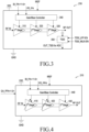
- FIG. 3 is a circuit diagram illustrating a detailed structure of a power amplifier, according to various embodiments of the present disclosure.
- the PA 216 e.g., the PA 216 of FIG. 2
- the PA 216 may include at least one of a plurality of amplifiers 310, 320, and 330, a gain/bias controller 340, or a TSSI 350.
- an RF signal input to the PA 216 may be amplified through the amplifiers 310, 320, and 330 of each stage, and a gain and/or a bias of each of the amplifiers 310, 320, and 330 may be controlled by the gain/bias controller 340.
- the gain/bias controller 340 may receive a control signal from the communication module (e.g., the communication module 112 of FIG. 1 ) or the processor (e.g., the processor 111 of FIG. 1 ) to control the gain and/or the bias of each of the amplifiers 310, 320, and 330.
- control signal provided from the communication module or the processor may be generated based on a parameter stored in the memory as calibration is performed on the second communication circuit (e.g., the second communication circuit 121 of FIG. 1 or the second communication circuit 200 of FIG. 2 ).
- a radio signal amplified by the amplifier 330 of the last stage among the plurality of amplifiers 310, 320, and 330 may be transmitted to a corresponding antenna, and may be provided to the TSSI 350 according to various embodiments.
- the TSSI 350 formed in a terminal of the PA 216 may be a circuit for detecting a power level, and may be used to calibrate the output power of the second communication circuit.
- a signal output from the TSSI 350 may be provided to an analog-to-digital converter (ADC0, and may perform calibration on the second communication circuit by comparing a digital value of a TSSI level with a preset value.
- ADC0 analog-to-digital converter
- FIG. 4 is a circuit diagram illustrating a detailed structure of a pre-processing power amplifier, according to various embodiments of the present disclosure.
- the PPA 215 e.g., the PPA 215 of FIG. 2
- the PPA 215 of FIG. 2 may include at least one of a plurality of amplifiers 410, 420, and 430 or a gain/bias controller 440.
- an RF signal input to the PPA 215 may be amplified through the amplifiers 410, 420, and 430 of each stage.
- a gain and/or a bias of each of the amplifiers 410, 420, and 430 may be controlled by the gain/bias controller 440.
- the gain/bias controller 440 may receive a control signal from the communication module (e.g., the communication module 112 of FIG. 1 ) or the processor (e.g., the processor 111 of FIG. 1 ) to control the gain and/or the bias of each of the amplifiers 410, 420, and 430.
- control signal provided from the communication module or the processor may be generated based on a parameter stored in the memory as calibration is performed on the second communication circuit (e.g., the second communication circuit 121 of FIG. 1 or the second communication circuit 200 of FIG. 2 ).
- a radio signal amplified by the amplifier 430 of the last stage among the plurality of amplifiers 410, 420, and 430 may be provided to an amplifier (e.g., the amplifier 310 of FIG. 3 ) of the first stage among the plurality of amplifiers included in the power amplifier (e.g., the PA 216 of FIG. 3 ).
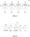
- FIG. 5 is a circuit diagram illustrating a detailed structure of a phase shifter, according to various embodiments of the present disclosure.
- the PS 214 e.g., the PS 214 or the PS 212 of FIG. 2
- the PS 214 may include at least one of a plurality of phase shifters 510, 520, 530, or 540.
- the PS 214 may function to change a phase of an input signal, and may change a phase of 0 - 360 degrees at intervals of 22.5 degrees into a total of 16 stages for 4 bits, as shown in FIG. 5 .
- FIG. 6 illustrates a transmission signal processing circuit according to various embodiments of the present disclosure.
- a transmission/reception signal processing circuit e.g., the transmission/reception processing circuit 210 of FIG. 2
- the divider 220b may divide power for the transmission/reception processing circuit 210 corresponding to each antenna and provide the power to the PSDA 213 of each transmission/reception processing circuit 210.
- a signal provided to the PSDA 213 may be amplified and then provided to the PS 214.
- the PS 214 may change a phase of the received signal based on a control signal and output the phase-changed signal to the PPA 215.
- the PPA 215 may amplify power at a stage previous to the PA 216 and then provide the amplified signal to the PA 216.
- the PA 216 may amplify the signal provided from the PPA 215 and provide the amplified signal to the antenna.
- the control signal generated based on a parameter set through calibration may control a gain and/or a bias of at least one of the PSDA 213, the PPA 215, or the PA 216 that constitute the transmission/reception processing circuit 210.
- the control signal may control a gain and/or a bias for at least one amplifier included in the PSDA 213, a gain and/or a bias for at least one amplifier included in the PPA 215, or a gain and/or a bias for at least one amplifier included in the PA 216.
- the parameter set through calibration may be set based on current and power measured for the entire second communication circuit 200 or may be set separately for each of the plurality of transmission/reception processing circuits 210.
- calibration may be performed on each of the plurality of transmission/reception processing circuits 210 connected to the plurality of antennas, and a parameter corresponding to a gain and/or a bias may be set for each of the plurality of (e.g., 16) transmission/reception processing circuits 210.
- power for each transmission/reception processing circuit 210 measured for calibration, may be obtained from an output signal of the PA 216 included in each transmission/reception processing circuit 210, and the designated transmission/reception processing circuit 210 may operate in calibration to sequentially measure current and/or power for each transmission/reception processing circuit 210.
- each parameter when calibration is performed on each transmission/reception circuit 210, each parameter may be stored in the memory to correspond to each transmission/reception processing circuit 210.
- an electronic device may include a housing, a plurality of antennas arranged on or inside the housing, a second communication circuit positioned inside the housing and electrically connected with the plurality of antennas, a first communication circuit electrically connected with the second communication circuit and configured to generate a signal in a radio frequency (RF) band (RF signal) or a signal in an intermediate frequency (IF) band(IF signal) and transmit the RF signal or the IF signal to the second communication circuit, a memory storing at least one parameter set corresponding to characteristics of the second communication circuit, and a control circuit electrically connected with the first communication circuit, in which the control circuit is configured to transmit a control signal for controlling at least one amplifier included in the second communication circuit to the second communication circuit, based on the at least one parameter stored in the memory.
- RF radio frequency
- IF intermediate frequency
- control signal may include a signal for controlling a gain and/or a bias of the at least one amplifier included in the second communication circuit.
- the electronic device may further include a communication device arranged inside the housing, in which the communication device includes the plurality of antennas and the second communication circuit.
- the memory may be included in the communication device.
- the second communication circuit may include at least one of a phase shifter drive amplifier (PSDA), a phase shifter (PS), a pre-power amplifier (PPA), or a power amplifier (PA).
- PSDA phase shifter drive amplifier
- PS phase shifter
- PPA pre-power amplifier
- PA power amplifier
- control signal may include a signal for controlling a gain and/or a bias of at least one of the PSDA, the PPA, or the PA.
- control signal may include a signal for controlling a gain and/or a bias of at least one amplifier included in the PSDA, a gain and/or a bias of at least one amplifier included in the PPA, or a gain and/or a bias of at least one amplifier included in the PA.
- the electronic device further includes a printed circuit board (PCB) arranged inside the housing, in which the first communication circuit and the control circuit are included in the PCB.
- PCB printed circuit board
- the electronic device further includes a first memory included in the second communication circuit and a second memory arranged on the PCB, in which the control circuit is configured to receive the at least one parameter stored in the memory and store the received at least one parameter in the second memory.
- the IF signal may correspond to a frequency between 8 GHz and 12 GHz and may be a frequency between an RF frequency and a local oscillator (LO) frequency (e.g., 5.x GHz).
- LO local oscillator
- the RF signal may correspond to a frequency between 25 GHz to 60 GHz.
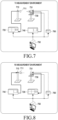
- FIG. 7 illustrates a transmission (TX) measurement environment for calibration, according to various embodiments of the present disclosure
- FIG. 8 illustrates a reception (RX) measurement environment for calibration, according to various embodiments of the present disclosure.
- a communication device 731 e.g., the communication device 120 of FIG. 1
- at least one of a PC 750, a signal generator 740, a signal analyzer 720, or a power supply 760 may be used.
- the communication device 731 in a module form may be fixed on a cradle 730, and a horn antenna 711 may be fixed on a cradle 710 to correspond to the communication device 731.
- a control signal generated through the PC 750 may be transmitted to the signal generator 740 that may generate a corresponding RF signal or IF signal based on the control signal transmitted from the PC 750.
- the RF signal or IF signal generated by the signal generator 740 may be provided to the communication device 731 placed on the cradle 730.
- the communication device 731 may include a second communication circuit (e.g., the second communication circuit 121 of FIG. 1 or the second communication circuit 200 of FIG. 2 ) and a plurality of array antennas (e.g., the array antenna 122 of FIG. 1 ).
- the communication device 731 may be provided with the RF signal or the IF signal from the signal generator 740 and transmit the RF signal or IF signal over the air (OTA) through the array antenna 122.
- the power supply 760 may supply power to each module (e.g., the PC 750, the signal generator 740, the signal analyzer 720, or the communication device 731) and may measure current consumed in each module based on the supplied power.
- the horn antenna 711 fixed on the cradle 710 to correspond to the communication device 731 may receive the RF signal transmitted from the communication device 731 and provide the RF signal received by the horn antenna 711 to the signal analyzer 720.
- the signal analyzer 720 may analyze the RF signal received by the horn antenna 711 and perform calibration on the communication device 731.
- a control signal generated through the PC 750 may be transmitted to the signal generator 740 that may generate a corresponding RF signal or IF signal based on the control signal transmitted from the PC 750.
- the RF signal or IF signal generated by the signal generator 740 may be provided to the horn antenna 711 placed on the cradle 710.
- the horn antenna 711 may transmit the RF signal over the air (OTA).
- the communication device 731 may include at least one array antenna (e.g., the array antenna 122 of FIG. 1 ) through which the communication device 731 may receive the RF signal transmitted from the horn antenna 711.
- the RF signal received by the communication device 731 may be provided to the signal analyzer 720.
- the signal analyzer 720 may analyze the RF signal received by the communication device 731 and perform calibration on the communication device 731.
- calibration may be performed.
- Results measured by the method may be expressed as [Table 1] and may be expressed graphs shown in FIGS. 9 and 10 .
- [Table 1] Initial Value Sample No. Current (A) EIRP(dBm) 1 0.22 23.99 2 0.219 23.87 3 0.235 25.60 4 0.28 28.26 5 0.259 26.44 6 0.246 25.71 7 0.316 29.14 8 0.288 27.98 9 0.228 24.03 10 0.24 25.97 11 0.239 25.87 12 0.286 28.57 13 0.24 25.94 14 0.274 27.91 15 0.236 25.84 16 0.208 22.58 17 0.226 24.13 18 0.203 22.90 19 0.23 24.12 20 0.232 24.60 Average (avg) 0.24525 25.6716 Minimum Value (min) 0.203 22.582 Maximum Value (max) 0.316 29.139
- FIG. 9 is a graph 900 showing current in maximum power for each sample according to various embodiments of the present disclosure
- FIG. 10 is a graph 1000 showing an effective isotopically radiated power (EIRP) for each sample according to various embodiments of the present disclosure.
- EIRP effective isotopically radiated power
- the generated EIRP difference may be reduced, and the EIRP may have a value within a specific range regardless of the second communication circuit or the communication device, thereby improving reliability of the second communication circuit or the communication device.
- FIGS. 11 to 14 a description will be made of a calibration method according to various embodiments of the present disclosure.
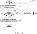
- FIG. 11 is a flowchart of a calibration method in an electronic device, according to various embodiments of the present disclosure.
- a measurement environment for the communication device shown in FIG. 7 or 8 may be set up.
- the electronic device may apply an RF signal or an IF signal to the communication device (e.g., the communication device 731 of FIG. 7 ) and measure power or current flowing in the communication device.
- the electronic device may adjust a gain and/or a bias in operation 1130.
- the measured value When current or power flowing in the communication device is measured in operation 1110, the measured value may change with adjustment of the gain or the bias.
- the changed measured value satisfies the preset condition in operation 1120, a parameter corresponding to a gain and/or a bias in case of satisfaction with the preset condition may be stored in the memory of the communication device in operation 1140.
- the electronic device when the electronic device including the communication device performs communication, the electronic device may control current or power of the communication device by using a parameter stored as a result of performing calibration on the communication device.
- FIG. 12 is a flowchart of a calibration method in an electronic device, according to various embodiments of the present disclosure.
- a measurement environment for the communication device e.g., the communication device 731 of FIG. 7
- a minimum value (min) of current for determining a defect of the communication device may be set.
- a minimum set value (set min) and a maximum set value (set max) for a target current range for performing calibration may be set.
- the electronic device may apply an RF signal or an IF signal to the communication device (e.g., the communication device 731 of FIG. 7 ) and measure power flowing in the communication device.
- measurement of the current may be performed from current consumed upon supply of the power to the communication device.
- the second communication circuit may be processed as a defect in operation 1230 because the second communication circuit is an unavailable communication circuit.
- an operation for calibration may be performed in operation 1240.
- the electronic device may adjust a gain and/or a bias in operation 1250.
- the measured value may change with adjustment of the gain or the bias.
- the changed measured value satisfies the preset condition (e.g., the measured value falls within a designated range) in operation 1240
- a parameter corresponding to a gain and/or a bias in case of satisfaction with the preset condition may be stored in the memory of the communication device in operation 1270.
- the electronic device when the electronic device including the communication device performs communication, the electronic device may control the current of the communication device by using a parameter stored as a result of performing calibration on the communication device.
- FIG. 13 is a flowchart of a calibration method in an electronic device, according to various embodiments of the present disclosure.
- a measurement environment for the communication device e.g., the communication device 731 of FIG. 7
- a maximum value (max) and a minimum value (min) of power for determining a defect of the communication device may be set up.
- a minimum set value (P min) and a maximum set value (P max) for a target power range for performing calibration may be set.
- the electronic device may apply an RF signal or an IF signal to the communication device (e.g., the communication device 731 of FIG. 7 ) and determine an ADC value for a TSSI of a signal output from the communication device.
- measurement of the TSSI may be performed based on a TSSI (e.g., the TSSI 350 of FIG. 3 ) included in the PA (e.g., the PA 216 of FIG. 2 ) included in the communication device.
- the communication device may be processed as a defect in operation 1330 because the communication device is an unavailable communication device.
- an operation for calibration may be performed in operation 1340.
- the electronic device may adjust a gain and/or a bias in operation 1350.
- the measured value may change with adjustment of the gain or the bias.
- the changed measured value satisfies the preset condition (e.g., the measured value falls within a designated range (set min ⁇ P ⁇ set max)) in operation 1340, a parameter corresponding to a gain and/or a bias in case of satisfaction with the preset condition may be stored in the memory of the communication device in operation 1370.
- the electronic device when the electronic device including the communication device performs communication, the electronic device may control the current of the communication device by using a parameter stored as a result of performing calibration on the communication device.
- FIG. 14 is a flowchart of a calibration method in an electronic device, according to various embodiments of the present disclosure.
- a measurement environment for the communication device e.g., the communication device 731 of FIG. 7
- a minimum value (min) of current and power for determining a defect of the communication device may be set respectively.
- the electronic device may apply an RF signal or an IF signal to the communication device (e.g., the communication device 731 of FIG. 7 ) and determine current of the communication device and an ADC value for a TSSI of a signal output from the communication device.
- measurement of the TSSI may be performed based on a TSSI (e.g., the TSSI 350 of FIG. 3 ) included in the PA (e.g., the PA 216 of FIG. 2 ) included in the communication device.
- measurement of the current may be performed by measuring current consumed upon supply of the power to the communication device.
- the second communication circuit may be processed as a defect in operation 1430 because the second communication circuit is an unavailable communication circuit.
- the result of the measurement falls in a range between the maximum value and the minimum value, which is a current condition for normal decision of the communication device in operation 1420, it may be determined whether power of the communication device satisfies the condition for normal decision.
- the communication device may be processed as a defect in operation 1450 because the communication device is an unavailable communication device.
- an operation for calibration may be performed in operation 1460.
- Operations 1420 and 1440 may be processed in an order shown in FIG. 14 , and operation 1440 may be performed first and then operation 1420 may be performed according to various embodiments.
- the electronic device may adjust a gain and/or a bias in operation 1470.
- the measured value may change with adjustment of the gain or the bias.
- the changed measured value satisfies the preset condition (e.g., the measured value falls within a designated range (set min ⁇ P ⁇ set max and/or set min ⁇ I ⁇ set max)) in operation 1460, a parameter corresponding to a gain and/or a bias in case of satisfaction with the preset condition may be stored in the memory of the communication device in operation 1490.
- the electronic device when the electronic device including the communication device performs communication, the electronic device may control the current of the communication device by using a parameter stored as a result of performing calibration on the communication device.
- FIG. 15 is a circuit diagram illustrating a structure of a second communication circuit, according to various embodiments of the present disclosure.
- the second communication circuit 1500 of FIG. 15 may further include a memory 1510 in addition to the above-described components of the second communication circuit 200 of FIG. 2 , and data corresponding to a result of calibration may be stored in the memory 1510.
- reference numerals that are the same as those of the blocks shown in FIG. 2 may perform the same functions and thus will not be described in detail.
- calibration data may be stored using any one of a memory configured in the second communication circuit 200 of FIG. 2 without addition of the memory 1510 in FIG. 15 .
- the memory 1510 capable of storing the calibration data may be added inside the second communication circuit shown in FIG. 2 .
- the memory 1510 included in the shown second communication circuit 1500 may also operate when the second communication circuit 1500 operates in a test mode for calibration.
- the transition switch 226 may switch to the test mode.
- a test signal Ext_Lo may be input to the transition switch 226 and the test signal input to the transition switch 226 may be provided to the transmission/reception signal processing circuit 210.
- the controller 230 may adjust a gain and/or a bias of each amplifier included in the transmission/reception signal processing circuit 210 in the test mode.
- a parameter for adjusting the gain and/or the bias of each amplifier may be stored in the memory 1510.
- the second communication circuit 1500 may be mounted in the electronic device to communicate with a first communication circuit (e.g., the first communication circuit 113 of FIG. 1 ).
- a first communication circuit e.g., the first communication circuit 113 of FIG. 1
- the processor e.g., the processor 111 of FIG. 1
- the communication module e.g., the communication module 112 of FIG. 1
- the processor may adjust a gain and/or a bias of at least one amplifier included in the second communication circuit 1500 based on the parameter stored in the memory 1510 of the second communication circuit 1500.
- the processor e.g., the processor 111 of FIG. 1
- the communication module e.g., the communication module 112 of FIG. 1
- the processor may read the parameter stored in the memory 1510 of the second communication circuit 1500 and store the read parameter in a memory arranged in a PCB (e.g., the PCB 110 of FIG. 1 ).
- the processor e.g., the processor 111 of FIG. 1
- the communication module e.g., the communication module 112 of FIG. 1
- the processor may adjust a gain and/or a bias of at least one amplifier included in the second communication circuit 1500 based on the parameter stored in the memory of the PCB 110.
- FIG. 16 is a flowchart showing operations of an electronic device, according to various embodiments of the present disclosure.
- a communication device on which calibration has been completed may be mounted on an electronic device.
- the electronic device may read a region of a memory (e.g., the memory 1510 of FIG. 15 ) of the second communication circuit (e.g., the second communication circuit 200 of FIG. 2 ).
- a memory e.g., the memory 1510 of FIG. 15
- the second communication circuit e.g., the second communication circuit 200 of FIG. 2 .
- a calibration correction procedure of a second communication circuit may be performed in operation 1630.
- a calibration parameter stored in the memory of the second communication circuit may be stored in a memory of a PCB (e.g., a main PCB) in operation 1640. According to various embodiments, operation 1640 may be omitted.
- the electronic device when the electronic device transmits and receives an RF signal through the second communication circuit, the electronic device may control the second communication circuit by using the calibration parameter stored in the memory of the PCB.
- a communication module (e.g., the communication module 112 of FIG. 1 ) of an electronic device may collect a parameter stored in a calibration data memory region of a second communication circuit and use the parameter in transmission or reception without changing a storage position of the parameter, or store the collected parameter in a memory region of a main PCB (e.g., the PCB 110 of FIG. 1 ) and use the parameter in transmission or reception.
- a main PCB e.g., the PCB 110 of FIG. 1
- an operation method of an electronic device includes generating, by a first communication circuit, a signal in a radio frequency (RF) band (RF signal) or a signal in an intermediate frequency (IF) band (IF signal), transmitting the RF signal or IF signal, generated by the first communication circuit, to a second communication circuit, transmitting a control signal, generated based on at least one parameter set corresponding to characteristics of the second communication circuit, to the second communication circuit, receiving, by the second communication circuit, the control signal and controlling at least one amplifier included in the second communication circuit based on the received control signal, and transmitting, by the second communication circuit, a signal amplified by the at least one amplifier to at least one array antenna.
- RF radio frequency
- IF intermediate frequency
- control signal may include a signal for controlling a gain and/or a bias of the at least one amplifier included in the second communication circuit.
- the electronic device may further include a communication device arranged inside the housing, in which the communication device may include the at least one array antenna and the second communication circuit.
- the at least one parameter may be uniquely set corresponding to the second communication circuit.
- the second communication circuit may include at least one of a phase shifter drive amplifier (PSDA), a phase shifter (PS), a pre-power amplifier (PPA), or a power amplifier (PA).
- PSDA phase shifter drive amplifier
- PS phase shifter
- PPA pre-power amplifier
- PA power amplifier
- control signal may include a signal for controlling a gain and/or a bias of at least one of the PSDA, the PPA, or the PA.
- control signal may include a signal for controlling a gain and/or a bias of at least one amplifier included in the PSDA, a gain and/or a bias of at least one amplifier included in the PPA, or a gain and/or a bias of at least one amplifier included in the PA.
- the electronic device further includes a printed circuit board (PCB) arranged inside the housing, in which the first communication circuit may be included in the PCB.
- PCB printed circuit board
- the electronic device further includes a first memory included in the second communication circuit and a second memory arranged on the PCB, in which the operation method may further include transmitting the at least one parameter stored in the first memory to the second memory.
- the IF signal may correspond to a frequency between 8 GHz and 12 GHz and the RF signal may correspond to a frequency between 25 GHz to 60 GHz.
- a current target set value for the calibration has been set to 240 mA as set min and 260 mA as set max.
- Results of [Table 3] may be expressed as graphs shown in FIGS. 17 and 18 .
- FIG. 17 is a graph 1700 showing calibrated current in maximum power for each sample according to various embodiments of the present disclosure
- FIG. 18 is a graph 1800 showing a calibrated EIRP for each sample according to various embodiments of the present disclosure.
- an EIRP result after calibration with respect to the communication device or the second communication circuit using current shows that a deviation between samples is adjusted from 6dBm or more to 2dBm or less when compared to a result before the calibration.
- an EIRP has a difference of 6.5dBm or more before calibration, but is reduced to 1.6dBm or less after calibration.
- FIG. 19 illustrates a TX measurement environment for calibration, according to various embodiments of the present disclosure.
- calibration may be performed without installation of the above-described equipment shown in FIGS. 7 and 8 .
- a control signal generated through a PC 1950 may be transmitted to a signal generator 1940 that may generate a corresponding RF signal or IF signal based on the control signal transmitted from the PC 1950.
- the RF signal or IF signal generated by the signal generator 1940 may be provided to a communication device 1931 (e.g., the communication device 731 of FIG. 7 or the second communication circuit 1500 of FIG. 15 ) placed on a cradle 1930.
- the communication device 1931 may include at least one array antenna (e.g., the array antenna 122 of FIG. 1 ) and may be provided with the RF signal or the IF signal from the signal generator 1940 and transmit the RF signal or IF signal over the air (OTA) through the array antenna 121.
- OTA air
- a power supply 1960 may supply power to the communication device 1931, and when the power is supplied to the communication device 1931, current flowing in the communication device 1931 through a supply line may be measured.
- a TSSI e.g., the TSSI 350 of FIG. 3
- PA e.g., the PA 216 of FIG. 2
- the calibration experiment has been performed on the twenty samples.
- calibration using current has been performed on twenty 5G mmWave RF modules.
- Current for defect decision has been set to 100 mA as a minimum value (min) and 400 mA as a maximum value (max).
- ACD Code EIRP(dBm) ACD Code EIRP(dBm) 1 34 23.96 48 26.01 2 35 23.81 49 25.61 3 46 25.49 4C 25.91 4 5A 28.11 4D 26.34 5 4E 26.53 4A 25.92 6 4A 25.64 49 25.81 7 60 29.01 4A 26.00 8 58 27.96 4C 26.35 9 35 24.12 48 25.14 10 4B 25.97 4B 26.33 11 49 25.81 49 25.74 12 59 28.61 4A 25.98 13 4A 25.88 4A 26.15 14 54 27.86 48 25.74 15 4B 25.95 4B 26.19 16 2A 22.61 49 24.85 17 38 24.31 49 25.75 18 2E 22.78 4A 25.67 19 3A 24.02 49 24.94 20 41 24.85 49 25.26 Average 25.66 25.78 Minimum Value 22.61 24.85 Maximum Value 29.01 26.35
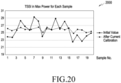
- FIG. 20 is a graph 2000 showing TSSI calibrated in maximum power for each sample, according to various embodiments of the present disclosure.
- an EIRP result after calibration with respect to the communication device using TSSI shows that a deviation between samples is adjusted from 6dBm or more to 2dBm or less when compared to a result before the calibration.
- an EIRP has a difference of 6.4dBm or more before calibration, but is reduced to 1.5dBm or less after calibration.
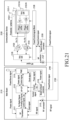
- FIG. 21 illustrates a structure of an electronic device according to various embodiments of the present disclosure.
- an electronic device may include a main board 2110 (e.g., a main PCB (e.g., the PCB 110 of FIG. 1 )) or a communication device 2120 (e.g., the communication device 120 of FIG. 1 or the communication device 731 of FIG. 7 ).
- a main board 2110 e.g., a main PCB (e.g., the PCB 110 of FIG. 1 )
- a communication device 2120 e.g., the communication device 120 of FIG. 1 or the communication device 731 of FIG. 7 .
- the main board 110 may include at least one of a first communication circuit (e.g., an RF transceiver) 2111, a processor (e.g., an AP or a CP) 2112, a power management IC (PMIC) 2113, an RF connector 2115, or a board connector 2116.
- a first communication circuit e.g., an RF transceiver
- a processor e.g., an AP or a CP
- PMIC power management IC
- the processor 2112 may be formed in a single chip or a plurality of chips.
- the processor 2112 may include a communication module (CP) (e.g., the communication module 112 of FIG. 1 ) and an AP (e.g., the processor 111 of FIG. 1 ).
- the processor 2112 may transmit and receive a control signal for power control to and from the PMIC 2113 and be provided with power from the PMIC 2113.
- CP communication module
- AP e.g., the processor 111 of FIG. 1
- the PMIC 2113 may be provided with power from a battery or a charger or from an external device through a power cable and supply power to each module or component included in the electronic device.
- the PMIC 2113 may provide power to the processor 2112, the first communication circuit 2111, or a temperature controlled crystal oscillator/crystal oscillator (TCXO/XO).
- the PMIC 2113 may supply power to the communication device 2120 through the board connector 2116.
- the processor 2112 may generate a signal to be transmitted through wireless communication as an analog I/Q signal and transmit the signal to the first communication circuit 2111.
- the first communication circuit 2111 may receive the analog I/Q signal from the processor 2112 and modulate the analog I/Q signal into an RF signal through a modulator.
- the first communication circuit 2111 may transmit the RF signal modulated by the modulator to the communication device 2120 through the RF connector 2115.
- the processor 2112 may transmit a control signal to the first communication circuit 2111 to control the first communication circuit 2111.
- the main board 2110 and the communication device 2120 may be connected through at least one cable.
- the RF connector 2115 of the main board 2110 may be connected with an RF connector 2127 of the communication device 2120 through a first cable 2130
- the board connector 2116 of the main board 2110 may be connected with a board connector 2128 of the communication device 2120 through a second cable 2140.
- the main board 2110 may transmit and receive the RF signal to and from the communication device 2120 through the first connector 2130.
- the main board 2110 may transmit a control signal and/or power to the communication device 2120 through the second connector 2140.
- the communication device 2120 may include at least one of a plurality of antenna elements 2121 (or array antennas), a plurality of front-end circuits 2122 connected corresponding to the plurality of antenna elements, a PA 2123, an LNA 2124, a transmission/reception switch 2125, or a controller 2126.
- the communication device 2120 may receive an RF signal transmitted from the main board 2110 through the RF connector 2127 and transmit the received RF signal to a transmission line through the transmission/reception switch 2125.
- the transmission/reception switch 2125 may switch to a transmission mode to transmit the received RF signal to the PA 2123.
- the PA 2123 may amplify the received RF signal and transmit the amplified RF signal to the plurality of front-end circuits 2122.
- Each front-end circuit 2122 may perform wireless signal processing through a PS, a PA, a transmission/reception switch, etc., included in the front-end circuit 2122, and then transmit the RF signal to each antenna element 2121.
- Each antenna element 2121 may transmit the RF signal wireless-signal-processed in each front-end circuit 2122 to a radio space.
- each antenna element 2121 When the communication device 2120 operates in a reception mode, the RF signal received through each antenna element 2121 may be transmitted to the front-end circuit 2122 connected to each antenna element 2121.
- Each front-end circuit 2122 may receive the RF signal from the antenna element 2121, perform wireless signal processing through a transmission/reception switch, an LNA, a PS etc., included in the front-end circuit 2122, and then transmit the RF signal to the LNA 2124.
- the LNA 2124 may amplify the received RF signal and low-noise amplify the RF signal for total system noise performance optimization.
- the LNA 2124 may transmit the RF signal to the main board 2110 through the RF connector 2127 via the transmission/reception switch 2125.
- the controller 2126 of the communication device 2120 may be provided with a control signal and power from the main board 2110 through the board connector 2128 and provide the control signal and the power to each component or circuit of the communication device 2120 or perform control.
- the controller 2126 may output the control signal to control at least one of the transmission/reception switch 2125, the PA 2123, the LNA 2124, or the front-end circuit 2122.
- the controller 2126 may generate a control signal based on a parameter set through calibration with respect to each communication device 2120. According to various embodiments, the controller 2126 may transmit the control signal to at least one amplifier included in the front-end circuit 2122 and control a gain and/or a bias of the at least one amplifier. According to various embodiments, the set parameter may be stored in a memory of the main board 2110 or in a memory of the communication device 2120.
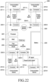
- FIG. 22 illustrates an internal structure of an electronic device according to various embodiments of the present disclosure.
- an electronic device 2200 may include a plurality of communication devices 2210 (e.g., the communication device 120 of FIG. 1 , the communication device 731 of FIG. 7 , or the communication device 2120 of FIG. 21 ), a main board 2220 (e.g., the PCB 110 of FIG. 1 ), and a battery 2230.
- Each of the plurality of communication devices 2210 may include an RF connector 2211 and a board connector 2212 as described above with reference to FIG. 21 , and may communicate in connection with an RF connector 2224 and a board connector 2225 included in the main board 2220.
- the communication device 2210 may include at least one array antenna, and may be formed, for example, in the form of a module including an array antenna.
- the main board 2220 may include at least one of a processor 2221, a PMIC 2222, a first communication circuit 2223, the RF connector 2224, the board connector 2225, or a camera module 2226.
- an analog transmission signal generated by the processor 2221 may be modulated into an RF signal or an IF signal by the first communication circuit 2223.
- the first communication circuit 2223 may transmit the modulated RF signal or IF signal to each communication device 2210 through each RF connector 2224.
- the processor 2221 may generate a control signal and transmit the control signal to each communication device 2210 through the board connector 2225.
- the PMIC 2222 may supply power to each communication device 2210 through the board connector 2225.
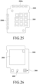
- FIG. 23A is a perspective view of a front surface of an electronic device, according to an embodiment
- FIG. 23B is a perspective view of a rear surface of the electronic device of FIG. 23A
- an electronic device 2300 e.g., the electronic device 2200 of FIG. 22
- the housing may refer to a structure that forms some of the first surface 2310A, the second surface 2310B, and the side surface 2310C of FIG. 23A .
- the first surface 2310A may be formed by a front plate 2302, at least a part of which is substantially transparent (for example, a glass plate including various coating layers or a polymer plate).
- the second surface 2310B is formed by a rear plate 2311 that is substantially opaque.
- the rear plate 2311 is formed by, for example, coated or painted glass, ceramic, polymer, metal (e.g., aluminum, stainless steel (STS), or magnesium) or a combination of at least two of the listed materials.
- the side surface 2310C is coupled with the front plate 2302 and the rear plate 2311, and is formed by a side bezel structure (or a "side member") 2318 including metal and/or polymer.
- the rear plate 2311 and the side bezel structure 2318 may be formed as one piece and may include the same material (e.g., a metal material such as aluminum).
- the electronic device 2300 may include at least one of a display 2301, audio modules 2303, 2307, and 2314, sensor modules 2304 and 2319, camera modules 2305, 2312, and 2313, key input devices 2315, 2316, and 2317, an indicator 2306, and connector holes 2308 and 2309.
- the electronic device 2300 may exclude at least one (e.g., the key input devices 2315, 2316, and 2317 or the indicator 2306) of the components or add other components.
- the display 2301 may be exposed through the most part of, for example, the front plate 2302.
- the display 2301 is coupled with or arranged in adjacent to a touch sensing circuit, a pressure sensor capable of measuring a strength (pressure) of a touch, and/or a digitizer for detecting a magnetic-type stylus pen.
- the audio modules 2303, 2307, and 2314 may include the microphone holes 2303 and the speaker holes 2307 and 2314. Inside the microphone hole 2303 may be arranged a microphone for obtaining external sound, and may also be arranged a plurality of microphones for sensing a direction of the sound in an embodiment. Th speaker holes 2307 and 2314 may include an external speaker hole 2307 and a call receiver hole 2314. In an embodiment, the speaker holes 2307 and 2314 and the microphone hole 2303 may be implemented as one hole or a speaker may be included without the speaker holes 2307 and 2314 (e.g., a piezo speaker).
- the sensor modules 2304 and 2319 generate an electrical signal or data value corresponding to an internal operating state or external environmental state of the electronic device 2300.
- the sensor modules 2304 and 2319 may include a first sensor module 2304 (e.g., a proximity sensor) and/or a second sensor module (not shown, e.g., a fingerprint sensor) arranged on the first surface 2310A of the housing 2310 and/or a third sensor module 2319 (e.g., a heart rate monitor (HRM) sensor) arranged on the second surface 2310B of the housing 2310.
- the fingerprint sensor may be arranged on the second surface 2310B of the housing 2310 as well as the first surface 2310A of the housing 210 (e.g., a home key button 2315).
- the electronic device 2300 may further include at least one of a sensor module not shown, e.g., a gesture sensor, a gyro sensor, an atmospheric pressure sensor, a magnetic sensor, an acceleration sensor, a grip sensor, a color sensor, an infrared (IR) sensor, a bio sensor, a temperature sensor, a humidity sensor, or an illuminance sensor.
- a sensor module not shown, e.g., a gesture sensor, a gyro sensor, an atmospheric pressure sensor, a magnetic sensor, an acceleration sensor, a grip sensor, a color sensor, an infrared (IR) sensor, a bio sensor, a temperature sensor, a humidity sensor, or an illuminance sensor.
- a sensor module not shown, e.g., a gesture sensor, a gyro sensor, an atmospheric pressure sensor, a magnetic sensor, an acceleration sensor, a grip sensor, a color sensor, an infrared (IR) sensor, a bio sensor, a temperature sensor
- the camera modules 2305, 2312, and 2313 may include a first camera device 2305 arranged on the first surface 2310A of the electronic device 2300, a second camera device 2312 arranged on the second surface 2310B, and/or a flash 2313.
- the camera modules 2305 and 2312 may include one lens or a plurality of lenses, an image sensor, and/or an image signal processor.
- a flash 2313 may include, for example, a light-emitting diode or a xenon lamp.
- two or more lenses (a wide lens and a telephoto lens) and image sensors may be arranged on a surface of the electronic device 2300.
- the key input devices 2315, 2316, and 2317 may include the home key button 2315 arranged on the first surface 2310A of the housing 2310, a touch pad 2316 arranged around the home key button 2315, and/or a side key button 2317 arranged on the side surface 2310C of the housing 2310.
- the electronic device 2300 may exclude some or all of the above-mentioned key input devices 2315, 2316, and 2317, and the excluded key input devices 2315, 2316, and 2317 may be implemented in other forms such as a soft key, etc., on the display 2301.
- the indicator 2306 may be arranged, for example, on the first surface 2310A of the housing 2310.
- the indicator 2306 may provide state information of the electronic device 2300 in the form of light, and may include a light-emitting diode (LED).
- LED light-emitting diode
- the connector holes 2308 and 2309 may include a first connector hole 2308 capable of accommodating a connector (e.g., a universal serial bus (USB) connector) for transmitting and receiving power and/or data with an external electronic device and/or a second connector hole (e.g., an earphone jack) 2309 capable of accommodating a connector for transmitting and receiving an audio signal with the external electronic device.
- a connector e.g., a universal serial bus (USB) connector
- USB universal serial bus
- FIG. 24 is a planar perspective view of the electronic device shown in FIGS. 23A and 23B .
- an electronic device 2400 e.g., the electronic device 2200 of FIG. 22
- a side bezel structure 2410 e.g., a first support member 2411 (e.g., a bracket), a front plate 2420, a display 2430, a printed circuit board (PCB) 2440, a battery 2450, a plurality of communication devices 2491, 2492, 2493, and 2494 (e.g., the communication
- the electronic device 2400 may exclude at least one (e.g., the first support member 2411 or the second support member 2460) of the components or add other components.
- the first support member 2411 is arranged inside the electronic device 2400 and is connected with the side bezel structure 2410 or is formed as one piece with the side bezel structure 2410.
- the first support member 2411 may be formed of, for example, a metal material and/or a non-metallic (e.g., polymer) material.
- the first support member 2411 is coupled with the display 2430 on a surface thereof and with the PCB 2440 on another surface thereof.
- On the PCB 2440 are mounted a processor, a memory, and/or an interface.
- the processor may include one or more of, for example, a central processing unit, an application processor, a graphic processor, an image signal processor, a sensor hub processor, or a communication processor.
- the memory may include, for example, a volatile and/or nonvolatile memory.
- An interface may include a high definition multimedia interface (HDMI), a universal serial bus (USB) interface, a secure digital (SD) card interface, and/or an audio interface.
- HDMI high definition multimedia interface
- USB universal serial bus
- SD secure digital
- the interface may electrically or physically connect, for example, the electronic device 2400 with an external electronic device, and may include an USB connector, an SD card/MMC connector, or an audio connector.
- the battery 2450 may be a device for supplying power to at least one component of the electronic device 2400.
- the battery 189 may include, e.g., a primary cell which is not rechargeable, a secondary cell which is rechargeable, or a fuel cell. At least a part of the battery 2400 may be arranged on substantially the same plane as, for example, the PCB 2440.
- the battery 2450 may be arranged as one piece inside the electronic device 2400 or may be arranged removably from the electronic device 2400.
- the antenna 2470 is arranged between the rear plate 2480 and the battery 2450.
- the antenna 2470 may include, for example, a near field communication (NFC) antenna, a wireless charging antenna, and/or a magnetic secure transmission (MST) antenna.
- the antenna 2470 may perform short-range communication or wirelessly transmit and receive power needed for charging, with, for example, an external device.
- an antenna structure may be formed by a part or a combination of the side bezel structure 2410 and/or the first support member 2411.
- the side bezel structure 2410, the first support member 2411, and the second support member 2460 may form a housing (e.g., the housing 2310 of FIG. 23 ) as a whole.
- the housing may support the PCB 2440 and the plurality of antenna modules 2491 through 2494.
- the housing may have the shape of a substantially flat plate.
- a part of the housing, e.g., at least a part of an edge thereof may have the shape of a curved surface.
- the housing may be at least partially formed of a metal material to supplement and improve the rigidity of the electronic device, provide a proper installation position of electronic parts, and provide installation positions for some electronic parts where the electronic parts are installed isolated from each other.
- the rear plate 2480 may be a part of the housing.
- the housing and the rear plate 2480 are described as separate components, but the rear plate 2480 may form a uni-body with the housing or may be a part of the housing.
- the plurality of communication devices 2491 through 2494 may include four communication devices, for example, a first communication device 2491, a second communication device 2492, a third communication device 2493, and a fourth communication device 2493.
- the first communication device 2491 and the second communication device 2492 may be implemented to transmit and receive RF signals (referred to as frequency signals A and B) having different characteristics for MIMO implementation.
- the first communication device 2491 and the third communication device 2493 may be configured to transmit and receive RF signals (referred to as frequency signals A1 and A2) having identical characteristics for diversity implementation, for example, at the same time.
- the second communication device 2492 and the fourth communication device 2494 may be configured to transmit and receive RF signals (referred to as frequency signals B1 and B2) having identical characteristics for diversity implementation, for example, at the same time.
- the plurality of antenna modules may include only two antenna modules, for example, the first communication device 2491 and the second communication device 2492, but in an example illustrated in FIG. 2 and other drawings, four communication devices 2491, 2492, 2493, and 2494 are included to implement MIMO and diversity at the same time.
- the second communication device 2492 when the first communication device 2491 may be arranged at a first position inside or on the housing, the second communication device 2492 may be arranged at a second position that is separated from the first position inside or on the housing.
- the first communication device 2491 and the third communication device 2493 may be arranged considering a distance therebetween corresponding to diversity or MIMO characteristics.
- the second communication device 2492 and the fourth communication device 2494 may also be arranged considering a distance therebetween inside or on the housing 210.
- the housing may include a front plate and a rear plate that is directed opposite to the front plate with respect to a radiation direction of the plurality of communication devices 2491 through 2494.
- the housing may have a rectangular shape including a first side having a first length, a second side having a second length longer than the first length, a third side having the first length, and a fourth side having the second length.
- the first communication device 2491 and the second communication device 2492 are arranged closer to the first side than the third side.
- the third communication device 2493 and the fourth communication device 2494 may be arranged closer to the third side than the first side when viewed from the top of the front plate of the housing.
- the first communication device 2492 and the third communication device 2493 may be arranged diagonally to each other when viewed from the top of the front plate of the housing in the rectangular shape.
- the second communication device 2492 and the fourth communication device 2494 may be arranged diagonally to each other when viewed from the top of the front plate of the housing.
- the plurality of communication devices 2491 through 2494 may be connected with an array antenna and the second communication circuit that is connected with the array antenna to process transmission and reception signals of ultra high frequencies.
- the array antenna may be implemented as, for example, a patch-type radiation element array (e.g., a 4x4 radiation element array).
- a chip having a part of the second communication circuit implemented therein may have a structure in which the chip is coupled for example, through PCB wiring, in a side surface or a lower side (a rear side with respect to the radiation direction) of the patch-type radiation element array.
- FIGS. 25 and 26 are views illustrating a structure of a communication device according to various embodiments of the present disclosure, and show an example of a structure applicable to, for example, the plurality of communication devices 2491 to 2494 of FIG. 24 .
- a communication device e.g., the communication device 120 of FIG. 1 , the communication device 731 of FIG. 7 , or the communication device 2120 of FIG. 21
- at least one array antenna 2591, 2592a, and 2592b may be formed on a first surface of one PCB 2500, and a chip 2693 having implemented therein a part of the second communication circuit may be arranged on a second surface of the one PCB 2500.
- the array antenna formed on the first surface of the PCB 2500 may include a total of 16 radiation elements including 8 patch-type radiation elements 2591 formed around the center of the first surface, 4 dipole-type radiation elements 2592a formed on a widthwise side surface of the PCB 2500, and 4 dipole-type radiation elements 2592b formed on a longitudinal side surface of the PCB 2500.
- the chip 2693 implementing a part of the second communication circuit, a coaxial cable connector 2695 for connection with a main PCB (the PCB 110 of FIG. 1 ), and a board-to-board (B-to-B) connector 2694 may be formed on the second surface of the PCB 2500.
- the PCB 2500 of the communication device may be connected with the main PCB (e.g., the PCB 110 of FIG. 1 ) through the coaxial cable by using the coaxial cable connector 2695, and the coaxial cable may be used mainly for transmission and reception RF signal transfer. Power or other control signals may be transferred through the B-to-B connector 2694.
- FIG. 27 is a block diagram illustrating an electronic device 2710 (e.g., the electronic device 2200 of FIG. 22 or the electronic device 2400 of FIG. 24 ) in a network environment 2700 according to various embodiments.
- the electronic device 2701 in the network environment 2700 may communicate with an electronic device 2702 via a first network 2798 (e.g., a short-range wireless communication network), or an electronic device 2704 or a server 2708 via a second network 2799 (e.g., a long-range wireless communication network).
- the electronic device 2701 may communicate with the electronic device 2704 via the server 2708.
- the electronic device 2701 may include a processor 2720 (e.g., the processor 111 of FIG.
- a memory 2730 an input device 2750, a sound output device 2755, a display device 2760, an audio module 2770, a sensor module 2776, an interface 2777, a haptic module 2779, a camera module 2780, a power management module 2788, a battery 2789, a communication module 2790 (e.g., the communication module 112 of FIG. 1 ), a subscriber identification module (SIM) 2796, and an antenna module 2797.
- at least one (e.g., the display device 2760 or the camera module 2780) of the components may be omitted from the electronic device 2701, or other components may be added in the electronic device 101.
- some components may be implemented to be integrated together, e.g., as if the sensor module 2776 (e.g., a fingerprint sensor, an iris sensor, or an illuminance sensor) is embedded in the display device 2760.
- the processor 2720 may drive, e.g., software (e.g., a program 2740) to control at least one other component (e.g., a hardware or software component) of the electronic device 2701 connected with the processor 2720 and may process or compute various data.
- the processor 2720 may load and process a command or data received from another component (e.g., the sensor module 2776 or the communication module 2790) on a volatile memory 2732, and the processor 120 may store resultant data in a non-volatile memory 2734.
- the processor 2720 may include a main processor 2721 (e.g., a central processing unit (CPU) or an application processor (AP)) and an auxiliary processor 2723 that is operable independently from the main processor 2721, and additionally or alternatively, the auxiliary processor 2723 may include an auxiliary processor 2723 (e.g., a graphics processing unit (GPU), an image signal processor, a sensor hub processor, or a communication processor) that consumes less power than the main processor 2721 or is specified for a designated function.
- the auxiliary processor 2723 may be operated separately from or embedded in the main processor 2721.
- the auxiliary processor 2723 may control at least some of functions or states related to at least one (e.g., the display device 2760, the sensor module 2776, or the communication module 2790) of the components of the electronic device 2701, instead of the main processor 2721 while the main processor 2721 is in an inactive (e.g., sleep) state or along with the main processor 2721 while the main processor 2721 is an active state (e.g., performing an application).
- the auxiliary processor 2723 e.g., an image signal processor or a communication processor
- the auxiliary processor 2723 may be implemented as part of another component (e.g., the camera module 2780 or the communication module 2790) functionally related to the auxiliary processor 2723.
- the memory 2730 may store various data used by at least one component (e.g., the processor 2720 or the sensor module 2776) of the electronic device 2701, e.g., software (e.g., the program 2740) and input data or output data for a command related to the software.
- the memory 2730 may include the volatile memory 2732 or the non-volatile memory 2734.
- the program 2740 may include, e.g., an operating system (OS) 2742, middleware 2744, or an application 2746.
- OS operating system
- middleware middleware
- application 2746 application
- the input device 2750 may be a device for receiving a command or data, which is to be used for a component (e.g., the processor 2720) of the electronic device 2701, from an outside (e.g., a user) of the electronic device 2701.
- the input device 50 may include, e.g., a microphone, a mouse, or a keyboard.
- the sound output device 2755 may be a device for outputting sound signals to the outside of the electronic device 2701, and may include, e.g., a speaker which is used for general purposes, such as playing multimedia or recording and playing, and a receiver used for call receiving purposes only. According to an embodiment, the receiver may be formed integrally or separately from the speaker.
- the display device 2760 may be a device for visually providing information to a user of the electronic device 2701.
- the display device 2760 may include, e.g., a display, a hologram device, or a projector and a control circuit for controlling the display, hologram device, or projector.
- the display 2760 may include a touch circuitry or a pressure sensor capable of measuring the strength of a pressure with respect to a touch.
- the audio module 2770 may convert a sound into an electrical signal and vice versa. According to an embodiment, the audio module 2770 may obtain the sound via the input device 2750, or output the sound via the sound output device 2755 or a headphone of an external electronic device (e.g., an electronic device 2702) wiredly or wirelessly coupled with the electronic device 2701.
- an external electronic device e.g., an electronic device 2702
- the sensor module 2776 may generate an electrical signal or data value corresponding to an internal operating state (e.g., power or temperature) or external environmental state of the electronic device 2701.
- the sensor module 2776 may include, e.g., a gesture sensor, a gyro sensor, an atmospheric pressure sensor, a magnetic sensor, an acceleration sensor, a grip sensor, a proximity sensor, a color sensor, an infrared (IR) sensor, a bio sensor, a temperature sensor, a humidity sensor, or an illuminance sensor.
- the interface 2777 may support a designated protocol enabling a wired or wireless connection with an external electronic device (e.g., the electronic device 2702).
- the interface 2777 may include a high definition multimedia interface (HDMI), a universal serial bus (USB) interface, a secure digital (SD) card interface, or an audio interface.
- HDMI high definition multimedia interface
- USB universal serial bus
- SD secure digital
- a connecting terminal 2778 may include a connector, e.g., an HDMI connector, a USB connector, an SD card connector, or an audio connector (e.g., a headphone connector), which is able to physically connect the electronic device 2701 with an external electronic device (e.g., the electronic device 2702).
- a connector e.g., an HDMI connector, a USB connector, an SD card connector, or an audio connector (e.g., a headphone connector), which is able to physically connect the electronic device 2701 with an external electronic device (e.g., the electronic device 2702).
- the haptic module 2779 may convert an electrical signal into a mechanical stimulus (e.g., a vibration or motion) or electrical stimulus which may be recognized by a user via his tactile sensation or kinesthetic sensation.
- the haptic module 2779 may include, e.g., a motor, a piezoelectric element, or an electric stimulator.
- the camera module 2780 may capture a still image or moving images.
- the camera module 2780 may include one or more lenses, an image sensor, an image signal processor, or a flash.
- the power management module 2788 may be a module for managing power supplied to the electronic device 2701.
- the power management module 188 may be configured as at least part of, e.g., a power management integrated circuit (PMIC).
- PMIC power management integrated circuit
- the battery 2789 may be a device for supplying power to at least one component of the electronic device 2701.
- the battery 2789 may include, e.g., a primary cell which is not rechargeable, a secondary cell which is rechargeable, or a fuel cell.
- the communication module 2790 may support establishing a wired or wireless communication channel between the electronic device 2701 and an external electronic device (e.g., the electronic device 2702, the electronic device 2704, or the server 2708) and performing communication through the established communication channel.
- the communication module 2790 may include one or more communication processors that are operated independently from the processor 2720 (e.g., an application processor) and supports wired or wireless communication.
- the communication module 2790 may include a wireless communication module 2792 (e.g., a cellular communication module, a short-range wireless communication module, or a GNSS communication module) or a wired communication module 2794 (e.g., an LAN communication module or a power-line communication module), and may communicate with the external electronic device via the first network 2798 (e.g., a short-range communication network, such as BluetoothTM, wireless-fidelity (Wi-Fi) direct, or infrared data association (IrDA)) or the second network 2799 (e.g., a long-range communication network, such as a cellular network, the Internet, or a computer network (e.g., an LAN or wide area network (WAN)).
- the above-enumerated types of communication modules 2790 may be implemented in a single chip, where at least some of the modules are integrated, or individually in separate chips.
- the wireless communication module 2792 may differentiate and authenticate the electronic device 2701 in the communication network using user information stored in the subscriber identification module 2796.
- the antenna module 2797 may include one or more antennas for transmitting or receiving a signal or power to/from an outside.
- the communication module 2790 e.g., the wireless communication module 2792
- At least some of the above-described components may be coupled mutually and communicate signals (e.g., commands or data) therebetween via an inter-peripheral communication scheme (e.g., a bus, general purpose input and output (GPIO), serial peripheral interface (SPI), or mobile industry processor interface (MIPI)).
- an inter-peripheral communication scheme e.g., a bus, general purpose input and output (GPIO), serial peripheral interface (SPI), or mobile industry processor interface (MIPI)
- commands or data may be transmitted or received between the electronic device 2701 and the external electronic device 2704 via the server 2708 coupled with the second network 2799.
- Each of the electronic device 2702 and the electronic device 2704 may be a device of the same type as, or a different type, from the electronic device 2701.
- some or all of operations performed by the electronic device 2701 may be performed in another electronic device or a plurality of other electronic devices.
- the electronic device 2701 may request an external electronic device to perform at least some functions associated with the function or the service, instead of or in addition to executing the function or the service.
- the external electronic device having received the request may execute the requested function or additional function and transfer the execution result to the electronic device 2701.
- the electronic device 2701 may then process or further process the received result to provide the requested function or service.
- a cloud computing, distributed computing, or client-server computing technology may be used, for example.
- each of the foregoing elements described in various embodiments of the present disclosure may be configured with one or more components, names of which may vary with a type of the electronic device.
- the electronic device may include at least one of the foregoing elements, some of which may be omitted or to which other elements may be added.
- some of the elements of the electronic device according to various embodiments may be integrated into one entity to perform functions of the corresponding elements in the same manner as before they are integrated.
- a term “module” used herein may mean, for example, a unit including one of or a combination of two or more of hardware, software, and firmware.
- the “module” may be interchangeably used with a unit, a logic, a logical block, a component, or a circuit.
- the “module” may be a minimum unit or a portion of an integrated component.
- the “module” may be a minimum unit or part thereof, adapted to perform one or more functions.
- the “module” may be implemented mechanically or electronically.
- the “module” according to the embodiments may include at least one of an application-specific integrated circuit (ASIC) chip, field-programmable gate arrays (FPGAs), and a programmable-logic device performing certain operations already known or to be developed.
- ASIC application-specific integrated circuit
- FPGAs field-programmable gate arrays
- At least a part of an apparatus e.g., modules or functions thereof
- a method e.g., operations
- a command stored in a computer-readable storage medium in the form of a programming module.
- the one or more processors may perform functions corresponding to the instructions.
- the computer-readable storage medium may be, for example, a memory.
- the computer readable recording medium includes hard disk, floppy disk, or magnetic media (e.g., a magnetic tape, optical media (e.g., compact disc read only memory (CD-ROM) or digital versatile disc (DVD), magneto-optical media (e.g., floptical disk), a hardware device (e.g., read-only memory (ROM), random access memory (RAM), flash memory, etc.), and so forth.
- the program instructions may include a machine language code created by a complier and a high-level language code executable by a computer using an interpreter.
- the foregoing hardware device may be configured to be operated as at least one software module to perform an operation of the present disclosure, or vice versa.
- Modules or programming modules according to various embodiments of the present disclosure may include one or more of the foregoing elements, have some of the foregoing elements omitted, or further include additional other elements. Operations performed by the modules, the programming modules or other elements according to various embodiments may be executed in a sequential, parallel, repetitive or heuristic manner. Also, some of the operations may be executed in different order or omitted, or may have additional different operations.
Landscapes
- Engineering & Computer Science (AREA)
- Physics & Mathematics (AREA)
- Computer Networks & Wireless Communication (AREA)
- Signal Processing (AREA)
- Electromagnetism (AREA)
- Nonlinear Science (AREA)
- Power Engineering (AREA)
- Transceivers (AREA)
Claims (10)
- Elektronische Vorrichtung, umfassend:ein Gehäuse;eine Vielzahl von Antennen (122-1, 122-N), die an oder innerhalb des Gehäuses angeordnet ist;eine Vielzahl von zweiten Kommunikationsschaltungen (121-1, 121-N, 1500), die jeweils innerhalb des Gehäuses positioniert und elektrisch mit der Vielzahl von Antennen verbunden ist;eine Leiterplatte, PCB, (110), die in dem Gehäuse angeordnet ist;eine erste Kommunikationsschaltung (113), die in der PCB enthalten ist, die elektrisch mit den zweiten Kommunikationsschaltungen verbunden und konfiguriert ist, um ein Signal in einem Funkfrequenz-, RF-Band, RF-Signal oder ein Signal in einem Zwischenfrequenz-, IF-Band, IF-Signal zu erzeugen und das RF-Signal oder das IF-Signal an die zweiten Kommunikationsschaltungen zu übertragen;einen ersten Speicher (1510), der in jeder aus der Vielzahl von zweiten Kommunikationsschaltungen enthalten ist und mindestens einen Parameter speichert, der während Kalibrierung von jeder aus der Vielzahl von zweiten Kommunikationsschaltungen erzeugt wird;einen zweiten Speicher, der an der PCB angeordnet ist; undeine Steuerschaltung (111), die in der PCB enthalten ist, die elektrisch mit der ersten Kommunikationsschaltung verbunden ist,wobei die Steuerschaltung für Folgendes konfiguriert ist:Empfangen des mindestens einen Parameters, der in dem ersten Speicher gespeichert ist;Speichern des empfangenen mindestens einen Parameters in dem zweiten Speicher; undÜbertragen eines Steuersignals zum Steuern von mindestens einem Verstärker, der in der Vielzahl von zweiten Kommunikationsschaltungen enthalten ist, an die Vielzahl von zweiten Kommunikationsschaltungen basierend auf dem mindestens einen Parameter, der in dem zweiten Speicher gespeichert ist.
- Elektronische Vorrichtung nach Anspruch 1, wobei das Steuersignal ein Signal zum Steuern einer Verstärkung und/oder einer Vorspannung des mindestens einen Verstärkers umfasst, der in der Vielzahl von zweiten Kommunikationsschaltungen enthalten ist.
- Elektronische Vorrichtung nach Anspruch 1, ferner umfassend eine Vielzahl von Kommunikationsvorrichtungen (120-1, 120-N), die innerhalb des Gehäuses angeordnet ist,
wobei die Vielzahl von Kommunikationsvorrichtungen jeweils die Vielzahl von Antennen und die Vielzahl von zweiten Kommunikationsschaltungen umfasst. - Elektronische Vorrichtung nach Anspruch 3, wobei der erste Speicher in jeder aus der Vielzahl von Kommunikationsvorrichtungen enthalten ist.
- Elektronische Vorrichtung nach Anspruch 1, wobei jede aus der Vielzahl von zweiten Kommunikationsschaltungen mindestens eines von einem Phasenschieber-Treiberverstärker, PSDA, einem Phasenschieber, PS, einem Vorleistungsverstärker, PPA, oder einem Leistungsverstärker, PA, umfasst.
- Elektronische Vorrichtung nach Anspruch 5, wobei das Steuersignal ein Signal zum Steuern einer Verstärkung und/oder einer Vorspannung von mindestens einem von dem PSDA, dem PPA oder dem PA umfasst.
- Elektronische Vorrichtung nach Anspruch 6, wobei das Steuersignal ein Signal zum Steuern einer Verstärkung und/oder einer Vorspannung von mindestens einem Verstärker, der in dem PSDA enthalten ist, einer Verstärkung und/oder einer Vorspannung von mindestens einem Verstärker, der in dem PPA enthalten ist, oder einer Verstärkung und/oder einer Vorspannung von mindestens einem Verstärker, der in dem PA enthalten ist, umfasst.
- Elektronische Vorrichtung nach Anspruch 1, wobei das IF-Signal einer Frequenz zwischen 8 GHz und 12 GHz entspricht und das RF-Signal einer Frequenz zwischen 25 GHz bis 60 GHz entspricht.
- Betriebsverfahren einer elektronischen Vorrichtung, die einen ersten Speicher, der in einer Vielzahl von zweiten Kommunikationsschaltungen enthalten ist, und einen zweiten Speicher beinhaltet, der an einer PCB der elektronischen Vorrichtung angeordnet ist, wobei das Betriebsverfahren Folgendes umfasst:Erzeugen, durch eine erste Kommunikationsschaltung, eines Signals in einem Funkfrequenz-, RF-Band, RF-Signals, oder eines Signals in einem Zwischenfrequenz-, IF-Band, IF-Signals;Übertragen des RF-Signals oder des IF-Signals, das durch die erste Kommunikationsschaltung erzeugt wird, an mindestens eine aus der Vielzahl von zweiten Kommunikationsschaltungen,Übertragen von mindestens einem Parameter, der in dem ersten Speicher gespeichert ist, der während Kalibrierung von jeder aus der Vielzahl von zweiten Kommunikationsschaltungen erzeugt wird, an den zweiten Speicher;Übertragen eines Steuersignals, das basierend auf mindestens einem Parameter aus der Vielzahl von zweiten Kommunikationsschaltungen erzeugt wird, an die Vielzahl von zweiten Kommunikationsschaltungen,Empfangen, durch die Vielzahl von zweiten Kommunikationsschaltungen, des Steuersignals und Steuern von mindestens einem Verstärker, der in der Vielzahl von zweiten Kommunikationsschaltungen enthalten ist, basierend auf dem empfangenen Steuersignal; undÜbertragen, durch die zweiten Kommunikationsschaltungen, eines Signals, das durch den mindestens einen Verstärker verstärkt wird, an eine Vielzahl von Antennen.
- Betriebsverfahren nach Anspruch 9, wobei die elektronische Vorrichtung ferner eine Vielzahl von Kommunikationsvorrichtungen umfasst, die innerhalb des Gehäuses angeordnet ist, und
die Vielzahl von Kommunikationsvorrichtungen jeweils die Vielzahl von Antennen und die Vielzahl von zweiten Kommunikationsschaltungen umfasst.
Applications Claiming Priority (2)
| Application Number | Priority Date | Filing Date | Title |
|---|---|---|---|
| KR1020170159630A KR102402641B1 (ko) | 2017-11-27 | 2017-11-27 | 전자 장치 및 전자 장치에서의 통신 장치 캘리브레이션 방법 |
| PCT/KR2018/014491 WO2019103511A1 (ko) | 2017-11-27 | 2018-11-23 | 전자 장치 및 전자 장치에서의 통신 장치 캘리브레이션 방법 |
Publications (3)
| Publication Number | Publication Date |
|---|---|
| EP3706337A1 EP3706337A1 (de) | 2020-09-09 |
| EP3706337A4 EP3706337A4 (de) | 2020-12-30 |
| EP3706337B1 true EP3706337B1 (de) | 2023-05-17 |
Family
ID=66632035
Family Applications (1)
| Application Number | Title | Priority Date | Filing Date |
|---|---|---|---|
| EP18881113.7A Active EP3706337B1 (de) | 2017-11-27 | 2018-11-23 | Elektronische vorrichtung und verfahren zur kalibrierung einer kommunikationsvorrichtung einer elektronischen vorrichtung |
Country Status (4)
| Country | Link |
|---|---|
| US (1) | US11463115B2 (de) |
| EP (1) | EP3706337B1 (de) |
| KR (1) | KR102402641B1 (de) |
| WO (1) | WO2019103511A1 (de) |
Families Citing this family (4)
| Publication number | Priority date | Publication date | Assignee | Title |
|---|---|---|---|---|
| KR20220008605A (ko) * | 2020-07-14 | 2022-01-21 | 삼성전자주식회사 | 신호 보정을 위한 전자 장치 및 방법 |
| KR102913156B1 (ko) * | 2020-11-11 | 2026-01-14 | 삼성전자 주식회사 | 송수신부 공급 전압을 캘리브레이션하는 통신 장치 및 이의 동작 방법 |
| KR102756543B1 (ko) | 2022-09-02 | 2025-01-21 | 현대모비스 주식회사 | 절연 통신 시 셀프 캘리브레이션 장치 및 방법 |
| WO2024085663A1 (ko) * | 2022-10-19 | 2024-04-25 | 삼성전자 주식회사 | 보안 연결을 제공하는 전자 장치 및 그 동작 방법 |
Citations (1)
| Publication number | Priority date | Publication date | Assignee | Title |
|---|---|---|---|---|
| US20070001756A1 (en) * | 2005-06-29 | 2007-01-04 | Trocke Robert S | System for reducing calibration time of a power amplifier |
Family Cites Families (11)
| Publication number | Priority date | Publication date | Assignee | Title |
|---|---|---|---|---|
| US5644316A (en) * | 1996-05-02 | 1997-07-01 | Hughes Electronics | Active phased array adjustment using transmit amplitude adjustment range measurements |
| US6178313B1 (en) | 1998-12-31 | 2001-01-23 | Nokia Mobile Phones Limited | Control of gain and power consumption in a power amplifier |
| US6812905B2 (en) * | 1999-04-26 | 2004-11-02 | Andrew Corporation | Integrated active antenna for multi-carrier applications |
| US8049662B2 (en) * | 2007-07-23 | 2011-11-01 | Aviation Communication&Surveillance Systems LLC | Systems and methods for antenna calibration |
| US8195118B2 (en) | 2008-07-15 | 2012-06-05 | Linear Signal, Inc. | Apparatus, system, and method for integrated phase shifting and amplitude control of phased array signals |
| US8121557B2 (en) * | 2008-12-02 | 2012-02-21 | Broadcom Corporation | Configurable RF sections for receiver and transmitter and methods for use therewith |
| WO2012125186A1 (en) | 2011-03-15 | 2012-09-20 | Intel Corporation | Conformal phased array antenna with integrated transceiver |
| US8692707B2 (en) | 2011-10-06 | 2014-04-08 | Toyota Motor Engineering & Manufacturing North America, Inc. | Calibration method for automotive radar using phased array |
| US10135482B2 (en) | 2016-03-23 | 2018-11-20 | Avago Technologies General Ip (Singapore) Pte. Ltd. | Wireless transceiver with remote frontend |
| KR102476051B1 (ko) * | 2016-04-22 | 2022-12-09 | 삼성전자주식회사 | 전자 장치 및 전자 장치의 안테나 전환 방법 |
| KR102694249B1 (ko) * | 2019-06-19 | 2024-08-12 | 삼성전자 주식회사 | 복수의 안테나들 중에서 지정된 무선 통신을 지원할 안테나를 선택하기 위한 전자 장치 |
-
2017
- 2017-11-27 KR KR1020170159630A patent/KR102402641B1/ko active Active
-
2018
- 2018-11-23 EP EP18881113.7A patent/EP3706337B1/de active Active
- 2018-11-23 US US16/766,105 patent/US11463115B2/en active Active
- 2018-11-23 WO PCT/KR2018/014491 patent/WO2019103511A1/ko not_active Ceased
Patent Citations (1)
| Publication number | Priority date | Publication date | Assignee | Title |
|---|---|---|---|---|
| US20070001756A1 (en) * | 2005-06-29 | 2007-01-04 | Trocke Robert S | System for reducing calibration time of a power amplifier |
Also Published As
| Publication number | Publication date |
|---|---|
| EP3706337A4 (de) | 2020-12-30 |
| WO2019103511A1 (ko) | 2019-05-31 |
| KR20190061347A (ko) | 2019-06-05 |
| US20210376869A1 (en) | 2021-12-02 |
| KR102402641B1 (ko) | 2022-05-27 |
| EP3706337A1 (de) | 2020-09-09 |
| US11463115B2 (en) | 2022-10-04 |
Similar Documents
| Publication | Publication Date | Title |
|---|---|---|
| US11728563B2 (en) | Antenna for wireless communication and electronic device including the same | |
| US10666327B2 (en) | Electronic device and method for correcting phase in electronic device | |
| EP3379647B1 (de) | Elektronische vorrichtung mit antenne | |
| KR102476765B1 (ko) | 안테나를 구비한 전자 장치 | |
| KR102442573B1 (ko) | 전자 장치 및 전자 장치에서의 전력 제어 방법 | |
| KR20180134528A (ko) | 안테나를 포함하는 전자 장치 | |
| KR20200043735A (ko) | 상향링크 기준 신호를 송신하기 위한 전자 장치 및 방법 | |
| EP3706337B1 (de) | Elektronische vorrichtung und verfahren zur kalibrierung einer kommunikationsvorrichtung einer elektronischen vorrichtung | |
| KR20180109509A (ko) | 다중 급전 안테나 및 그것을 포함하는 전자 장치 | |
| US11114762B2 (en) | Method of outputting a signal using an antenna disposed adjacent to a conductive member of a connector and an electronic device using the same | |
| US20230387573A1 (en) | Electronic device comprising antenna | |
| KR20200122887A (ko) | 5g 통신에서의 전원 제어 방법 및 이를 위한 전자 장치 | |
| US20210013920A1 (en) | Device and method for calibrating communication module | |
| KR20180013099A (ko) | 무선 통신 성능을 개선하기 위한 방법 및 그 전자 장치 | |
| US20190036212A1 (en) | Antenna device and electronic device comprising same | |
| KR102360496B1 (ko) | 신호 위상을 보상하는 전자 장치 및 그 방법 | |
| US20210257748A1 (en) | Device and method for identifying status of external electronic device | |
| KR102844973B1 (ko) | 안테나를 포함하는 전자 장치 및 상기 전자 장치의 전력 백 오프 제어 방법 | |
| EP4037210A1 (de) | Sondenantennenbestimmungsverfahren und -gerät | |
| KR20200070782A (ko) | 외부 물체의 위치 및 접촉 여부를 감지하기 위한 전자 장치 | |
| US12089384B2 (en) | Electronic device | |
| US20240007135A1 (en) | Electronic device for providing dual connectivity | |
| US20230239018A1 (en) | Electronic device comprising antenna | |
| KR20240043020A (ko) | 복수의 안테나들을 포함하는 전자 장치에서 안테나의 설정을 제어하는 방법 및 이를 지원하는 전자 장치 | |
| KR20210116081A (ko) | 빔포밍을 위한 전자 장치 및 그의 동작 방법 |
Legal Events
| Date | Code | Title | Description |
|---|---|---|---|
| STAA | Information on the status of an ep patent application or granted ep patent |
Free format text: STATUS: THE INTERNATIONAL PUBLICATION HAS BEEN MADE |
|
| PUAI | Public reference made under article 153(3) epc to a published international application that has entered the european phase |
Free format text: ORIGINAL CODE: 0009012 |
|
| STAA | Information on the status of an ep patent application or granted ep patent |
Free format text: STATUS: REQUEST FOR EXAMINATION WAS MADE |
|
| 17P | Request for examination filed |
Effective date: 20200601 |
|
| AK | Designated contracting states |
Kind code of ref document: A1 Designated state(s): AL AT BE BG CH CY CZ DE DK EE ES FI FR GB GR HR HU IE IS IT LI LT LU LV MC MK MT NL NO PL PT RO RS SE SI SK SM TR |
|
| AX | Request for extension of the european patent |
Extension state: BA ME |
|
| A4 | Supplementary search report drawn up and despatched |
Effective date: 20201126 |
|
| RIC1 | Information provided on ipc code assigned before grant |
Ipc: H04B 17/13 20150101AFI20201120BHEP Ipc: H04B 17/10 20150101ALI20201120BHEP Ipc: H03G 3/30 20060101ALI20201120BHEP |
|
| DAV | Request for validation of the european patent (deleted) | ||
| DAX | Request for extension of the european patent (deleted) | ||
| STAA | Information on the status of an ep patent application or granted ep patent |
Free format text: STATUS: EXAMINATION IS IN PROGRESS |
|
| 17Q | First examination report despatched |
Effective date: 20211119 |
|
| GRAP | Despatch of communication of intention to grant a patent |
Free format text: ORIGINAL CODE: EPIDOSNIGR1 |
|
| STAA | Information on the status of an ep patent application or granted ep patent |
Free format text: STATUS: GRANT OF PATENT IS INTENDED |
|
| INTG | Intention to grant announced |
Effective date: 20221209 |
|
| GRAS | Grant fee paid |
Free format text: ORIGINAL CODE: EPIDOSNIGR3 |
|
| GRAA | (expected) grant |
Free format text: ORIGINAL CODE: 0009210 |
|
| STAA | Information on the status of an ep patent application or granted ep patent |
Free format text: STATUS: THE PATENT HAS BEEN GRANTED |
|
| AK | Designated contracting states |
Kind code of ref document: B1 Designated state(s): AL AT BE BG CH CY CZ DE DK EE ES FI FR GB GR HR HU IE IS IT LI LT LU LV MC MK MT NL NO PL PT RO RS SE SI SK SM TR |
|
| REG | Reference to a national code |
Ref country code: GB Ref legal event code: FG4D |
|
| REG | Reference to a national code |
Ref country code: DE Ref legal event code: R096 Ref document number: 602018050054 Country of ref document: DE |
|
| REG | Reference to a national code |
Ref country code: CH Ref legal event code: EP |
|
| REG | Reference to a national code |
Ref country code: IE Ref legal event code: FG4D |
|
| REG | Reference to a national code |
Ref country code: AT Ref legal event code: REF Ref document number: 1568830 Country of ref document: AT Kind code of ref document: T Effective date: 20230615 |
|
| REG | Reference to a national code |
Ref country code: LT Ref legal event code: MG9D |
|
| REG | Reference to a national code |
Ref country code: NL Ref legal event code: MP Effective date: 20230517 |
|
| REG | Reference to a national code |
Ref country code: AT Ref legal event code: MK05 Ref document number: 1568830 Country of ref document: AT Kind code of ref document: T Effective date: 20230517 |
|
| PG25 | Lapsed in a contracting state [announced via postgrant information from national office to epo] |
Ref country code: SE Free format text: LAPSE BECAUSE OF FAILURE TO SUBMIT A TRANSLATION OF THE DESCRIPTION OR TO PAY THE FEE WITHIN THE PRESCRIBED TIME-LIMIT Effective date: 20230517 Ref country code: PT Free format text: LAPSE BECAUSE OF FAILURE TO SUBMIT A TRANSLATION OF THE DESCRIPTION OR TO PAY THE FEE WITHIN THE PRESCRIBED TIME-LIMIT Effective date: 20230918 Ref country code: NO Free format text: LAPSE BECAUSE OF FAILURE TO SUBMIT A TRANSLATION OF THE DESCRIPTION OR TO PAY THE FEE WITHIN THE PRESCRIBED TIME-LIMIT Effective date: 20230817 Ref country code: NL Free format text: LAPSE BECAUSE OF FAILURE TO SUBMIT A TRANSLATION OF THE DESCRIPTION OR TO PAY THE FEE WITHIN THE PRESCRIBED TIME-LIMIT Effective date: 20230517 Ref country code: ES Free format text: LAPSE BECAUSE OF FAILURE TO SUBMIT A TRANSLATION OF THE DESCRIPTION OR TO PAY THE FEE WITHIN THE PRESCRIBED TIME-LIMIT Effective date: 20230517 Ref country code: AT Free format text: LAPSE BECAUSE OF FAILURE TO SUBMIT A TRANSLATION OF THE DESCRIPTION OR TO PAY THE FEE WITHIN THE PRESCRIBED TIME-LIMIT Effective date: 20230517 |
|
| PG25 | Lapsed in a contracting state [announced via postgrant information from national office to epo] |
Ref country code: RS Free format text: LAPSE BECAUSE OF FAILURE TO SUBMIT A TRANSLATION OF THE DESCRIPTION OR TO PAY THE FEE WITHIN THE PRESCRIBED TIME-LIMIT Effective date: 20230517 Ref country code: PL Free format text: LAPSE BECAUSE OF FAILURE TO SUBMIT A TRANSLATION OF THE DESCRIPTION OR TO PAY THE FEE WITHIN THE PRESCRIBED TIME-LIMIT Effective date: 20230517 Ref country code: LV Free format text: LAPSE BECAUSE OF FAILURE TO SUBMIT A TRANSLATION OF THE DESCRIPTION OR TO PAY THE FEE WITHIN THE PRESCRIBED TIME-LIMIT Effective date: 20230517 Ref country code: LT Free format text: LAPSE BECAUSE OF FAILURE TO SUBMIT A TRANSLATION OF THE DESCRIPTION OR TO PAY THE FEE WITHIN THE PRESCRIBED TIME-LIMIT Effective date: 20230517 Ref country code: IS Free format text: LAPSE BECAUSE OF FAILURE TO SUBMIT A TRANSLATION OF THE DESCRIPTION OR TO PAY THE FEE WITHIN THE PRESCRIBED TIME-LIMIT Effective date: 20230917 Ref country code: HR Free format text: LAPSE BECAUSE OF FAILURE TO SUBMIT A TRANSLATION OF THE DESCRIPTION OR TO PAY THE FEE WITHIN THE PRESCRIBED TIME-LIMIT Effective date: 20230517 Ref country code: GR Free format text: LAPSE BECAUSE OF FAILURE TO SUBMIT A TRANSLATION OF THE DESCRIPTION OR TO PAY THE FEE WITHIN THE PRESCRIBED TIME-LIMIT Effective date: 20230818 |
|
| PG25 | Lapsed in a contracting state [announced via postgrant information from national office to epo] |
Ref country code: FI Free format text: LAPSE BECAUSE OF FAILURE TO SUBMIT A TRANSLATION OF THE DESCRIPTION OR TO PAY THE FEE WITHIN THE PRESCRIBED TIME-LIMIT Effective date: 20230517 |
|
| PG25 | Lapsed in a contracting state [announced via postgrant information from national office to epo] |
Ref country code: SK Free format text: LAPSE BECAUSE OF FAILURE TO SUBMIT A TRANSLATION OF THE DESCRIPTION OR TO PAY THE FEE WITHIN THE PRESCRIBED TIME-LIMIT Effective date: 20230517 |
|
| PG25 | Lapsed in a contracting state [announced via postgrant information from national office to epo] |
Ref country code: SM Free format text: LAPSE BECAUSE OF FAILURE TO SUBMIT A TRANSLATION OF THE DESCRIPTION OR TO PAY THE FEE WITHIN THE PRESCRIBED TIME-LIMIT Effective date: 20230517 Ref country code: SK Free format text: LAPSE BECAUSE OF FAILURE TO SUBMIT A TRANSLATION OF THE DESCRIPTION OR TO PAY THE FEE WITHIN THE PRESCRIBED TIME-LIMIT Effective date: 20230517 Ref country code: RO Free format text: LAPSE BECAUSE OF FAILURE TO SUBMIT A TRANSLATION OF THE DESCRIPTION OR TO PAY THE FEE WITHIN THE PRESCRIBED TIME-LIMIT Effective date: 20230517 Ref country code: EE Free format text: LAPSE BECAUSE OF FAILURE TO SUBMIT A TRANSLATION OF THE DESCRIPTION OR TO PAY THE FEE WITHIN THE PRESCRIBED TIME-LIMIT Effective date: 20230517 Ref country code: DK Free format text: LAPSE BECAUSE OF FAILURE TO SUBMIT A TRANSLATION OF THE DESCRIPTION OR TO PAY THE FEE WITHIN THE PRESCRIBED TIME-LIMIT Effective date: 20230517 Ref country code: CZ Free format text: LAPSE BECAUSE OF FAILURE TO SUBMIT A TRANSLATION OF THE DESCRIPTION OR TO PAY THE FEE WITHIN THE PRESCRIBED TIME-LIMIT Effective date: 20230517 |
|
| PGFP | Annual fee paid to national office [announced via postgrant information from national office to epo] |
Ref country code: DE Payment date: 20231023 Year of fee payment: 6 |
|
| REG | Reference to a national code |
Ref country code: DE Ref legal event code: R097 Ref document number: 602018050054 Country of ref document: DE |
|
| PLBE | No opposition filed within time limit |
Free format text: ORIGINAL CODE: 0009261 |
|
| STAA | Information on the status of an ep patent application or granted ep patent |
Free format text: STATUS: NO OPPOSITION FILED WITHIN TIME LIMIT |
|
| 26N | No opposition filed |
Effective date: 20240220 |
|
| PG25 | Lapsed in a contracting state [announced via postgrant information from national office to epo] |
Ref country code: SI Free format text: LAPSE BECAUSE OF FAILURE TO SUBMIT A TRANSLATION OF THE DESCRIPTION OR TO PAY THE FEE WITHIN THE PRESCRIBED TIME-LIMIT Effective date: 20230517 |
|
| PG25 | Lapsed in a contracting state [announced via postgrant information from national office to epo] |
Ref country code: SI Free format text: LAPSE BECAUSE OF FAILURE TO SUBMIT A TRANSLATION OF THE DESCRIPTION OR TO PAY THE FEE WITHIN THE PRESCRIBED TIME-LIMIT Effective date: 20230517 Ref country code: IT Free format text: LAPSE BECAUSE OF FAILURE TO SUBMIT A TRANSLATION OF THE DESCRIPTION OR TO PAY THE FEE WITHIN THE PRESCRIBED TIME-LIMIT Effective date: 20230517 |
|
| REG | Reference to a national code |
Ref country code: CH Ref legal event code: PL |
|
| PG25 | Lapsed in a contracting state [announced via postgrant information from national office to epo] |
Ref country code: MC Free format text: LAPSE BECAUSE OF FAILURE TO SUBMIT A TRANSLATION OF THE DESCRIPTION OR TO PAY THE FEE WITHIN THE PRESCRIBED TIME-LIMIT Effective date: 20230517 |
|
| PG25 | Lapsed in a contracting state [announced via postgrant information from national office to epo] |
Ref country code: LU Free format text: LAPSE BECAUSE OF NON-PAYMENT OF DUE FEES Effective date: 20231123 |
|
| PG25 | Lapsed in a contracting state [announced via postgrant information from national office to epo] |
Ref country code: CH Free format text: LAPSE BECAUSE OF NON-PAYMENT OF DUE FEES Effective date: 20231130 |
|
| GBPC | Gb: european patent ceased through non-payment of renewal fee |
Effective date: 20231123 |
|
| PG25 | Lapsed in a contracting state [announced via postgrant information from national office to epo] |
Ref country code: MC Free format text: LAPSE BECAUSE OF FAILURE TO SUBMIT A TRANSLATION OF THE DESCRIPTION OR TO PAY THE FEE WITHIN THE PRESCRIBED TIME-LIMIT Effective date: 20230517 Ref country code: LU Free format text: LAPSE BECAUSE OF NON-PAYMENT OF DUE FEES Effective date: 20231123 Ref country code: CH Free format text: LAPSE BECAUSE OF NON-PAYMENT OF DUE FEES Effective date: 20231130 |
|
| REG | Reference to a national code |
Ref country code: BE Ref legal event code: MM Effective date: 20231130 |
|
| REG | Reference to a national code |
Ref country code: IE Ref legal event code: MM4A |
|
| PG25 | Lapsed in a contracting state [announced via postgrant information from national office to epo] |
Ref country code: IE Free format text: LAPSE BECAUSE OF NON-PAYMENT OF DUE FEES Effective date: 20231123 |
|
| PG25 | Lapsed in a contracting state [announced via postgrant information from national office to epo] |
Ref country code: GB Free format text: LAPSE BECAUSE OF NON-PAYMENT OF DUE FEES Effective date: 20231123 |
|
| PG25 | Lapsed in a contracting state [announced via postgrant information from national office to epo] |
Ref country code: BE Free format text: LAPSE BECAUSE OF NON-PAYMENT OF DUE FEES Effective date: 20231130 |
|
| PG25 | Lapsed in a contracting state [announced via postgrant information from national office to epo] |
Ref country code: FR Free format text: LAPSE BECAUSE OF NON-PAYMENT OF DUE FEES Effective date: 20231130 |
|
| PG25 | Lapsed in a contracting state [announced via postgrant information from national office to epo] |
Ref country code: IE Free format text: LAPSE BECAUSE OF NON-PAYMENT OF DUE FEES Effective date: 20231123 Ref country code: GB Free format text: LAPSE BECAUSE OF NON-PAYMENT OF DUE FEES Effective date: 20231123 Ref country code: FR Free format text: LAPSE BECAUSE OF NON-PAYMENT OF DUE FEES Effective date: 20231130 Ref country code: BE Free format text: LAPSE BECAUSE OF NON-PAYMENT OF DUE FEES Effective date: 20231130 |
|
| PG25 | Lapsed in a contracting state [announced via postgrant information from national office to epo] |
Ref country code: BG Free format text: LAPSE BECAUSE OF FAILURE TO SUBMIT A TRANSLATION OF THE DESCRIPTION OR TO PAY THE FEE WITHIN THE PRESCRIBED TIME-LIMIT Effective date: 20230517 |
|
| PG25 | Lapsed in a contracting state [announced via postgrant information from national office to epo] |
Ref country code: BG Free format text: LAPSE BECAUSE OF FAILURE TO SUBMIT A TRANSLATION OF THE DESCRIPTION OR TO PAY THE FEE WITHIN THE PRESCRIBED TIME-LIMIT Effective date: 20230517 |
|
| REG | Reference to a national code |
Ref country code: DE Ref legal event code: R119 Ref document number: 602018050054 Country of ref document: DE |
|
| PG25 | Lapsed in a contracting state [announced via postgrant information from national office to epo] |
Ref country code: CY Free format text: LAPSE BECAUSE OF FAILURE TO SUBMIT A TRANSLATION OF THE DESCRIPTION OR TO PAY THE FEE WITHIN THE PRESCRIBED TIME-LIMIT; INVALID AB INITIO Effective date: 20181123 |
|
| PG25 | Lapsed in a contracting state [announced via postgrant information from national office to epo] |
Ref country code: HU Free format text: LAPSE BECAUSE OF FAILURE TO SUBMIT A TRANSLATION OF THE DESCRIPTION OR TO PAY THE FEE WITHIN THE PRESCRIBED TIME-LIMIT; INVALID AB INITIO Effective date: 20181123 |
|
| PG25 | Lapsed in a contracting state [announced via postgrant information from national office to epo] |
Ref country code: DE Free format text: LAPSE BECAUSE OF NON-PAYMENT OF DUE FEES Effective date: 20250603 |
|
| PG25 | Lapsed in a contracting state [announced via postgrant information from national office to epo] |
Ref country code: TR Free format text: LAPSE BECAUSE OF FAILURE TO SUBMIT A TRANSLATION OF THE DESCRIPTION OR TO PAY THE FEE WITHIN THE PRESCRIBED TIME-LIMIT Effective date: 20230517 |