EP3704497B1 - Procédé pour effectuer la comparaison entre un signal analogique de valeur continue et un signal numérique de valeur continue et architecture de circuit configurée pour mettre en oeuvre le procédé précité - Google Patents
Procédé pour effectuer la comparaison entre un signal analogique de valeur continue et un signal numérique de valeur continue et architecture de circuit configurée pour mettre en oeuvre le procédé précité Download PDFInfo
- Publication number
- EP3704497B1 EP3704497B1 EP18811347.6A EP18811347A EP3704497B1 EP 3704497 B1 EP3704497 B1 EP 3704497B1 EP 18811347 A EP18811347 A EP 18811347A EP 3704497 B1 EP3704497 B1 EP 3704497B1
- Authority
- EP
- European Patent Office
- Prior art keywords
- value
- signal
- digital
- ramp
- analogue
- Prior art date
- Legal status (The legal status is an assumption and is not a legal conclusion. Google has not performed a legal analysis and makes no representation as to the accuracy of the status listed.)
- Active
Links
Images



Classifications
-
- G—PHYSICS
- G01—MEASURING; TESTING
- G01R—MEASURING ELECTRIC VARIABLES; MEASURING MAGNETIC VARIABLES
- G01R19/00—Arrangements for measuring currents or voltages or for indicating presence or sign thereof
- G01R19/0038—Circuits for comparing several input signals and for indicating the result of this comparison, e.g. equal, different, greater, smaller (comparing pulses or pulse trains according to amplitude)
Definitions
- the invention relates to a method for making the comparison between a continuous value analogue signal and a continuous value digital signal.
- the invention also relates to a circuit architecture configured to carry out the aforesaid method of the invention.
- information within the fields of electronics and informatics may be represented mainly in two ways: by means of analogue type signals or by means of numerical or digital type signals.
- the information content with the first is represented by the values that the physical signal may take on, and therefore it continuously varies within the dynamics of the signal.
- the information content in the case of digital signals instead is again represented by the values that the physical signal may take on, but in this case the significant values are a finite set.
- the processing of digital type signals instead provides acting on the information extracted from the physical signal transporting it.
- the digital (or numerical) processing of the signal therefore intrinsically processes discrete-time and discrete-value signals.
- the analogue processing limits of the analogue signals consist in having to build circuits capable of directly acting on the analogue signals themselves.
- a further limit of this type of processing is due to the presence of the intrinsic noise in the analogue signal or caused by the analogue processing circuit built to process the signal itself.
- the background art possibly also provides carrying out the conversion in opposite direction, and that is to convert the digital signal into a corresponding analogue signal, and then to compare them by means of a conveniently built analogue circuit system.
- Prior art US4484291 and US3409830 teach circuits that compare two analog signals, the latter using ramp signals.
- Prior art WO2017/076748 and US2013/099090 teach ramp-comparator type ADC's for imaging pixel arrays.
- the present invention intends overcoming all the drawbacks mentioned.
- the object of the invention is to define a method and propose a circuit architecture for making the comparison between a continuous value analogue signal and a continuous value digital signal which allows having a smaller voltage consumption with respect to a method and relative comparison circuit of the purely analogue type.
- the object of the invention is to define a method and propose a circuit architecture which allow reducing the silicone area occupied with respect to a method and a relative comparison circuit of the purely digital type.
- the aforesaid objects are achieved by the method of the invention for making the comparison between a continuous value analogue signal and a continuous value digital signal having the features according to independent claim 1.
- Such objects are also achieved by the circuit architecture configured to carry out the aforesaid method of the invention, having the features according to claim 8.
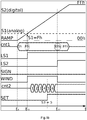
- time diagrams in figures 1a and 1b depict the signals involved in carrying out the method of the invention according to a preferred implementation embodiment thereof
- time diagrams in figures 2a and 2b depict the signals considered during the execution of the method of the invention according to an alternative implementation embodiment thereof.
- figures 1a and 2a hypothesize the execution of the method of the invention with the analogue signal S1 having a greater value with respect to the value of the digital signal S2.
- Figures 1b and 2b instead hypothesize the opposite situation, that is in the case in which the analogue signal S1 has a lesser value with respect to the value of the digital signal S2.
- the analogue signals considered are voltage signals.
- the analogue signals it is not excluded for the analogue signals to be current signals in further implementation embodiments alternative to the ones above.
- ramp analogue signal RAMP having linearly variable value over time.
- ramp analogue signal RAMP in particular is of the type which increases linearly over time.
- Such definition of the ramp analogue signal RAMP requires periodically varying, for each time interval belonging to first predetermined time intervals ck1, a first digital numerical value cnt1 by a predetermined quantity, and also providing to convert such first digital numerical value cnt1 into the aforesaid ramp analogue signal RAMP by means of a digital/analogue converter.
- the ramp analogue signal RAMP of the linearly increasing type is obtained by increasing the first digital numerical value cnt1 - preferably initialized at the value "0" - by such predefined quantity, which usually is selected equal to one unit.
- the ramp analogue signal RAMP is defined so that it is a linearly decreasing ramp analogue signal.
- Such a decreasing trend is obtained by decreasing the aforesaid first digital numerical value cnt1 initialized at a predefined positive value, by such predefined quantity, which preferably is selected equal to one unit.
- the method of the invention also provides simultaneously comparing the value of the ramp analogue signal RAMP with the analogue signal S1 and the first digital numerical value cnt1 with the digital signal S2 at each of such first predetermined time intervals ck1.
- the method of the invention is capable of temporally defining which of the aforesaid equalities occurs first and which occurs second, and is also capable of defining the time window WIND between the first equality and the second equality.
- figure 1a which provides an increase of the first digital numerical value cnt1 and accordingly, a linear increase of the ramp analogue signal RAMP - that the execution of the method of the invention allows identifying the equality of the digital signal S2 with such first digital numerical value cnt1 at a time interval ck1 prior to the time interval ck1 in which the equality occurs between the analogue signal S1 and the ramp analogue signal RAMP.
- figure 1b that is the execution of the method of the invention allows identifying the equality between the analogue signal S1 and the ramp analogue signal RAMP before the equality between the digital signal S2 with such first digital numerical value cnt1.
- FIG 2a which, as mentioned above, depicts the alternative implementation embodiment of the method of the invention with the first digital numerical value cnt1 of decreasing type and accordingly the ramp analogue signal RAMP of increasing type
- the execution of the same method allows first identifying the equality between the analogue signal S1 and the ramp analogue signal RAMP and then the equality between the digital signal S2 with such first digital numerical value cnt1.
- the execution of the method of the invention allows first identifying the equality of the digital signal S2 with the first digital numerical value cnt1 and then the equality between the analogue signal S1 and the ramp analogue signal RAMP.
- the comparison operation at each of the first predetermined time intervals ck1 of the value of the ramp analogue signal RAMP with the analogue signal S1 consists in inputting the aforesaid two analogue signals into an analogue comparator, and it provides commuting, in output, a first output signal LS1 from a first value to a second value at the time interval ck1 in which the value of the ramp analogue signal RAMP equals the analogue signal S1.
- the method of the invention further provides keeping such first output signal LS1 constant at the aforesaid second value following such commutation.
- the alternative implementation embodiment provides carrying out the same comparison method and treating the first output signal LS1 in the same way as the preferred implementation embodiment described above.
- the method provides comparing each bit representing the first digital numerical value cnt1 with the bit in the same position representing the digital signal S2, at each of the predetermined time intervals ck1.
- Such comparison further provides commuting a second output signal LS2 from a first value to a second value at the time interval ck1 in which all the bits of the first digital numerical value cnt1 equal the corresponding bits of the digital signal S2, and keeping the second output signal LS2 constant at such second value following such commutation.
- the alternative implementation embodiment of the method of the invention provides carrying out the same comparison method and treating the second output signal LS2 in the same way as that provided by the preferred implementation embodiment.
- step of defining the time order of the aforesaid equalities it provides comparing the first output signal LS1 and the second output signal LS2 and establishing which of the two output signs LS1 and LS2 commutes first.
- the method of the invention provides defining a time window WIND between the moment in time ck1 in which the first of the aforesaid commutations occurs and the moment in time in which the second commutation occurs.
- the method provides increasing, during the aforesaid time window WIND, a second digital numerical value cnt2, preferably initialized at "0" before the beginning of the same time window WIND.
- a second digital numerical value cnt2 preferably initialized at "0" before the beginning of the same time window WIND.
- Such an increase in particular occurs within the aforesaid time window WIND for each time interval belonging to second predetermined time intervals ck2.
- the duration of each time interval belonging to the aforesaid second predetermined time intervals ck2 could be equal to or less than the duration of each time interval belonging to the first predetermined time intervals ck1.
- such second digital numerical value cnt2 is increased during the time window WIND and at the closing of the latter the same second digital numerical value cnt2 represents the final deviation value between the analogue signal S1 and the digital signal S2.
- the method of the invention provides the further step - always performed at each of the aforesaid second time intervals ck2 - of comparing the second digital numerical value cnt2 with a predetermined threshold value DELTA so as to verify if and when the same second digital numerical value cnt2 equals the predetermined threshold DELTA.
- the comparison operation of the second digital numerical value cnt2 with a predetermined threshold digital value DELTA at each of the second predetermined time intervals ck2 provides comparing each bit representing the second digital numerical value cnt2 with the bit in the same position, which represents the predetermined threshold digital value DELTA.
- the method of the invention provides commuting a third output signal SET from a first value to a second value at the time interval belonging to the second predetermined time intervals ck2 in which all the bits of the second digital numerical value cnt2 equal the corresponding bits of the predetermined threshold digital value DELTA and keeping the third output signal SET constant at the second value following such commutation.
- circuit architecture 1 depicted diagrammatically in figure 3 is now introduced; it is configured to carry out the comparison method of the invention between a continuous value analogue signal S1 and a continuous value digital signal S2.
- such circuit architecture 1 comprises a first binary counter 2 configured to generate and periodically vary at first predetermined time intervals ck1 of the aforesaid first digital numerical value cnt1.
- such first binary counter 2 uses one byte (8 bits) to define the aforesaid first digital numerical value cnt1.
- the circuit architecture 1 also comprises a digital/analogue converter 3 operatively connected at the output of the first binary counter 2 so that the same digital/analogue converter 3 generates, in output, the ramp analogue signal RAMP having linearly variable value over time starting from such first digital numerical value cnt1.
- such first binary counter 2 and the relative digital/analogue converter 3 could already be present and used for other logic functions performed in the chip in which the aforesaid circuit architecture 1 of the invention is implemented.
- the implementation of the circuit architecture 1 of the invention advantageously could take advantage of the common circuit components usually present and used for multiple functions, thus avoiding to make the latter specifically.
- the circuit architecture 1 also comprises a first logical comparison group 4 configured to make the comparison between the value of the ramp analogue signal RAMP with the analogue signal S1 and to verify at which of the first predetermined time intervals ck1 the analogue signals S1 and RAMP equal one other.
- the first logical comparison group 4 in particular comprises an analogue comparator 41 with a first input 41a connected to the digital/analogue converter 3 to receive, in input, the ramp analogue signal RAMP, and with a second input 41b configured to receive, in input, the analogue signal S1.
- a first electronic storage circuit 42 is operatively connected downstream of such analogue comparator 41.
- Such first electronic storage circuit 42 is operatively connected with its input 42a to the output 41c of the analogue comparator 41.
- the first electronic storage circuit 42 is configured to commute the first output signal LS1 from a first value to a second value at the time interval ck1 in which the analogue comparator 41 detects the equality between the value of the ramp analogue signal RAMP and the analogue signal S1. Moreover, such first electronic storage circuit 42 is configured to keep the first output signal LS1 constant at the aforesaid second value following such commutation.
- the first electronic storage circuit 42 is provided with an output 42b for making available the aforesaid first output signal LS1.
- the circuit architecture 1 of the invention also comprises a second logical comparison group 5 configured to make the comparison between the first digital numerical value cnt1 and the digital signal S2, and to verify at which of the first predetermined time intervals ck1 the digital signals S2 and cnt1 equal one other.
- the second logical comparison group 5 comprises a number of logic gates 51 of "XNOR" type equal to the number of bits with which the first digital numerical value cnt1 and the digital signal S2 are defined.
- Each of the aforesaid "XNOR" logic gates 51 is configured to receive, in input, bits having same position as the first digital numerical value cnt1 and the digital signal S2. Moreover, the totality of the "XNOR” logic gates 51 have their own outputs arranged at the input of a logical block 52 of "AND” type so as to obtain, at the output 52a of such logical block 52 of “AND” type, a logical value "1" at the time interval ck1 in which all the bits of the first digital numerical value cnt1 equal the corresponding bits of the digital signal S2. Obviously, also such logical block 52 of "AND” type belongs to the second logical comparison group 5.
- the same second logical comparison group 5 comprises a second electronic storage circuit 53 operatively connected with its input 53a to the output 52a of the logical block 52 of "AND" type.
- the second electronic storage circuit 53 in particular is configured to commute the aforesaid second output signal LS2 from a first value to a second value when the output 52a of the logical block 52 of "AND" type is equal to "1".
- the same second electronic storage circuit 53 is configured to keep the second output signal LS2 constant at such second value following the aforesaid commutation.
- the second electronic storage circuit 53 is provided with an output 53b for making available the second output signal LS2.
- the circuit architecture 1 of the invention comprises also a third logical comparison group 6 configured to temporally define which of the two aforesaid equalities occurs first and which occurs second, and to define, further, the aforesaid time window WIND between the first equality and the second equality.
- the third logical comparison group 6 comprises a first logic gate 61 of "AND” type configured to receive, in input, the first output signal LS1 and the negated of the second output signal LS2N and a second logic gate 62 of "AND” type configured to receive, in input, the negated of the same first output signal LS1N and the second output signal LS2.
- the third logical comparison group 6 comprises a logic gate 63 of "OR” type configured to receive, in input, the outputs of the first logic gate 61 of “AND” type and of the second logic gate 62 of “AND” type so as to obtain the logical value "1" on its output 63a for a time period that defines the time window WIND.
- the third logical comparison group 6 comprises a third storage circuit 64 operatively connected with its input 64a, with the output exclusively of one between the first logic gate 61 of "AND” type and the second logic gate 62 of “AND” type.
- Such third storage circuit 64 is configured to commute its output 64b from a first value to a second value and to keep such output constant to the aforesaid second value in the case in which it receives, in input, the logical value "1" from the logic gate of "AND” type to which it is connected.
- the aforesaid third storage circuit 64 is configured to establish the sign of what was defined above as deviation between the analogue signal S1 and the digital signal S2.
- circuit architecture 1 of the invention provides a fourth logical comparison group 7 comprising a second binary counter 71 configured to generate and periodically vary the aforesaid second digital numerical value cnt2 at second predetermined time intervals ck2 during the time window WIND.
- Such fourth logical comparison group 7 is configured to compare the second digital numerical value cnt2 with a predetermined threshold value DELTA at each of the aforesaid second time intervals ck2 so as to verify if and when the same second digital numerical value cnt2 equals the aforesaid predetermined threshold DELTA.
- such second binary counter 71 is connected with its enabling input 71a with the output 63a of the logic gate 63 of "OR" type of the third logical comparison group 6 so that the same second binary counter 71 generates and periodically varies the value of the second digital numerical value cnt2 exclusively during the aforesaid time window WIND.
- the fourth logical comparison group 7 comprises a number of logic gates 72 of "XNOR" type equal to the number of bits with which the second digital numerical value cnt2 and the predetermined threshold value DELTA are defined.
- Each of the "XNOR” logic gates 72 is configured to receive, in input, the bit of the same position as the second digital numerical value cnt2 and as the predetermined threshold value DELTA.
- such "XNOR" logic gates 72 have their outputs arranged in input at a logical block 73 of "AND” type so as to obtain, in output 73a from the same logical block 73 of "AND” type, a logical value "1" at the time interval belonging to the aforesaid second predetermined time intervals ck2 in which all the bits of the second digital numerical value cnt2 equal the corresponding bits of the predetermined threshold value DELTA.
- the fourth logical comparison group 7 also comprises the aforesaid logical block 73 of "AND” type. Moreover, the fourth logical comparison group 7 comprises a fourth electronic storage circuit 74 operatively connected with its input 74a to the output 73a of the same logical block 73 of "AND” type. According to the invention, such fourth electronic storage circuit 74 is configured to commute the third output signal SET from a first value to a second value when the output 73a of the logical block 73 of "AND" type is equal to "1". Furthermore, the fourth electronic storage circuit 74 is configured to keep such third output signal SET constant at the aforesaid second value following such commutation.
- the fourth electronic storage circuit 74 is provided with an output 74b so as to make such third output signal SET available to the outside for further processing.
- the object is achieved of defining a method and proposing a circuit architecture for making the comparison between a continuous value analogue signal and a continuous value digital signal which allow having a smaller voltage consumption with respect to a method and a relative comparison circuit of the purely analogue type.
- the object is also achieved of defining a method and proposing a relative circuit architecture which allow ensuring increased flexibility in selecting and varying the value of the second signal - for example a threshold value - to be compared with the first signal, with respect to a method and a related comparison circuit of purely analogue type.
- the further object is achieved of defining a method and proposing a circuit architecture which allow reducing the number of integrated electronic components required for the implementation thereof with respect to a method and a relative comparison circuit of purely digital type.
- the object was also achieved of defining a method and proposing a circuit architecture which allow reducing the silicon area occupied with respect to a method and a relative comparison circuit of the purely digital type.
Landscapes
- Physics & Mathematics (AREA)
- General Physics & Mathematics (AREA)
- Analogue/Digital Conversion (AREA)
Claims (13)
- Procédé pour faire la comparaison entre un signal analogique à valeur continue (S1) et un signal numérique à valeur continue (S2), caractérisé en ce qu'il prévoit les étapes suivantes:- définir un signal analogique de rampe (RAMP) ayant une valeur variable linéairement dans le temps, ladite définition prévoyant de varier périodiquement, pour chaque intervalle de temps appartenant à des premiers intervalles de temps (ck1) prédéterminés, une première valeur numérique chiffrée (cnt1) d'une quantité prédéterminée, et prévoyant de convertir ladite première valeur numérique chiffrée (cnt1) en ledit signal analogique de rampe (RAMP) au moyen d'un convertisseur numérique/ analogique;- comparer simultanément, au niveau de chacun desdits premiers intervalles de temps (ck1) prédéterminés, la valeur dudit signal analogique de rampe (RAMP) avec ledit signal analogique (S1) et ladite première valeur numérique chiffrée (cnt1) avec ledit signal numérique (S2);- vérifier au niveau duquel desdits premiers intervalles de temps (ck1) prédéterminés ladite valeur dudit signal analogique de rampe (RAMP) est égale audit signal analogique (S1) et au niveau duquel desdits intervalles de temps (ck1) prédéterminés ladite première valeur numérique chiffrée (cnt1) est égale audit signal numérique (S2);- définir temporairement laquelle desdites égalités se produit en premier et laquelle se produit en deuxième et définir également la plage temporelle (WIND) entre ladite première égalité et ladite deuxième égalité;- augmenter une deuxième valeur numérique chiffrée (cnt2) à l'intérieur de ladite plage temporelle (WIND) pour chaque intervalle de temps appartenant à des deuxièmes intervalles de temps (ck2) prédéterminés, ladite deuxième valeur numérique chiffrée (cnt2) représentant la déviation entre ledit signal analogique (S1) et ledit signal numérique (S2);- comparer, au niveau de chacun desdits deuxièmes intervalles de temps (ck2), ladite deuxième valeur numérique chiffrée (cnt2) avec une valeur de seuil (DELTA) prédéterminée de façon à vérifier si et quand ladite deuxième valeur numérique chiffrée (cnt2) est égale audit seuil (DELTA) prédéterminé.
- Procédé selon la revendication 1, caractérisé en ce que ladite étape de définir ledit signal analogique de rampe (RAMP) prévoit:- d'augmenter ladite première valeur numérique chiffré (cnt1) de ladite quantité prédéfinie;- de convertir ladite première valeur numérique chiffrée (cnt1) de sorte que ledit signal analogique de rampe (RAMP) soit un signal analogique de rampe augmentant linéairement.
- Procédé selon la revendication 1, caractérisé en ce que ladite étape de définir ledit signal analogique de rampe (RAMP) prévoit:- de diminuer ladite première valeur numérique chiffrée (cnt1) à partir d'une valeur positive prédéfinie de ladite quantité prédéfinie;- de convertir ladite première valeur numérique chiffrée (cnt1) de sorte que ledit signal analogique de rampe (RAMP) soit un signal analogique de rampe diminuant linéairement.
- Procédé selon l'une quelconque des revendications précédentes, caractérisé en ce que ladite opération de comparaison au niveau de chacun desdits premiers intervalles de temps (ck1) prédéterminés de la valeur dudit signal analogique de rampe (RAMP) avec ledit signal analogique (S1) prévoit d'introduire lesdits signaux analogiques (S1, RAMP) à l'entrée d'un comparateur analogique, ladite comparaison prévoyant en outre de commuter, à la sortie, un premier signal de sortie (LS1) d'une première valeur à une deuxième valeur au niveau de l'intervalle de temps (ck1) dans lequel la valeur dudit signal analogique de rampe (RAMP) est égal audit signal analogique (S1), et de maintenir ledit premier signal de sortie (LS1) constant à ladite deuxième valeur suite à ladite commutation.
- Procédé selon l'une quelconque des revendications précédentes, caractérisé en ce que ladite opération de comparaison au niveau de chacun desdits premiers intervalles de temps (ck1) prédéterminés de ladite première valeur numérique chiffrée (cnt1) avec ledit signal numérique (S2) prévoit de comparer chaque bit représentant ladite première valeur numérique chiffrée (cnt1) avec le bit dans la même position représentant ledit signal numérique (S2), ladite comparaison prévoyant en outre de commuter un deuxième signal de sortie (LS2) d'une première valeur à une deuxième valeur au niveau de l'intervalle de temps (ck1) dans lequel tous les bits de ladite première valeur numérique chiffrée (cnt1) sont égaux aux bits correspondants dudit signal numérique (S1), et de maintenir ledit deuxième signal de sortie (LS2) constant à ladite deuxième valeur suite à ladite commutation.
- Procédé selon l'une quelconque des revendications précédentes, caractérisé en ce que ladite étape de définir l'ordre temporel desdites égalités prévoit de comparer ledit premier signal de sortie (LS1) et ledit deuxième signal de sortie (LS2) et d'établir lequel desdits signaux de sortie (LS1, LS2) commute en premier.
- Procédé selon l'une quelconque des revendications précédentes, caractérisé en ce que ladite opération de comparaison de ladite deuxième valeur numérique chiffrée (cnt2) avec une valeur numérique de seuil (DELTA) prédéterminée au niveau de chacun desdits deuxièmes intervalles de temps (ck2) prédéterminés prévoit:- de comparer chaque bit représentant ladite deuxième valeur numérique chiffrée (cnt2) avec le bit dans la même position représentant ladite valeur numérique de seuil (DELTA) prédéterminée;- de commuter un troisième signal de sortie (SET) d'une première valeur à une deuxième valeur au niveau de l'intervalle de temps appartenant auxdits deuxièmes intervalles de temps (ck2) prédéterminés dans lequel tous les bits de ladite deuxième valeur numérique chiffrée (cnt2) sont égaux aux bits correspondants de ladite valeur numérique de seuil (DELTA) prédéterminée, et de maintenir ledit troisième signal de sortie (SET) constant à ladite deuxième valeur suite à ladite commutation.
- Architecture de circuit (1) configurée pour réaliser le procédé de comparaison entre un signal analogique à valeur continue (S1) et un signal numérique à valeur continue (S2) selon l'une quelconque des revendications précédentes, caractérisée en ce qu'elle comprend:- un premier compteur binaire (2) configuré pour générer et varier périodiquement au niveau de premiers intervalles de temps (ck1) prédéterminés de ladite première valeur numérique chiffrée (cnt1);- un convertisseur numérique/analogique (3) connecté opérationnellement à la sortie dudit premier compteur binaire (2), ledit convertisseur numérique/ analogique (3) étant configuré pour générer, à la sortie, ledit signal analogique de rampe (RAMP) ayant une valeur variable linéairement dans le temps;- un premier groupe de comparaison logique (4) configuré pour faire la comparaison entre ladite valeur dudit signal analogique de rampe (RAMP) avec ledit signal analogique (S1) et pour vérifier au niveau duquel desdits premiers intervalles de temps (ck1) prédéterminés lesdits signaux analogiques (S1, RAMP) sont égaux entre eux;- un deuxième groupe de comparaison logique (5) configuré pour faire la comparaison entre ladite première valeur numérique chiffrée (cnt1) et ledit signal numérique (S2) et pour vérifier au niveau duquel desdits premiers intervalles de temps (ck1) prédéterminés lesdits signaux numériques (S2, cnt1) sont égaux entre eux;- un troisième groupe de comparaison logique (6) configuré pour définir temporairement laquelle desdites égalités se produit en premier et laquelle se produit en deuxième et pour définir ladite plage temporelle (WIND) entre ladite première égalité et ladite deuxième égalité;- un quatrième groupe de comparaison logique (7) comprenant un deuxième compteur binaire (71) configuré pour générer et varier périodiquement au niveau de deuxièmes intervalles de temps (ck2) prédéterminés de ladite deuxième valeur numérique chiffrée (cnt2) pendant ladite plage temporelle (WIND), ledit quatrième groupe de comparaison logique (7) étant configuré pour comparer, au niveau de chacun desdits deuxièmes intervalles de temps (ck2) prédéterminés, ladite deuxième valeur numérique chiffrée (cnt2) avec une valeur de seuil (DELTA) prédéterminée de façon à vérifier si et quand ladite deuxième valeur numérique chiffrée (cnt2) est égale audit seuil (DELTA) prédéterminé.
- Architecture de circuit (1) selon la revendication 8, caractérisée en ce que ledit premier groupe de comparaison logique (4) comprend:- un comparateur analogique (41) avec une première entrée (41a) connectée audit convertisseur numérique/analogique (3) pour recevoir, en entrée, ledit signal analogique de rampe (RAMP), et avec une deuxième entrée (41b) configurée pour recevoir, en entrée, ledit signal analogique (S1);- un premier circuit électronique de stockage (42) connecté opérationnellement avec son entrée (42a) à la sortie (41c) dudit comparateur analogique (41), ledit premier circuit électronique de stockage (42) étant configuré pour commuter ledit premier signal de sortie (LS1) d'une première valeur à une deuxième valeur au niveau de l'intervalle de temps (ck1) dans lequel un comparateur analogique (41) détecte ladite égalité entre la valeur dudit signal analogique de rampe (RAMP) et ledit signal analogique (S1), et pour maintenir ledit premier signal de sortie (LS1) constant à ladite deuxième valeur suite à ladite commutation, ledit premier circuit électronique de stockage (42) étant pourvu d'une sortie (42b) pour ledit premier signal de sortie (LS1).
- Architecture de circuit selon l'une quelconque des revendications 8 ou 9, caractérisée en ce que ledit deuxième groupe de comparaison logique (5) comprend:- un nombre de portes logiques (51) de type "XNOR" égal au nombre de bits avec lesquels ladite première valeur numérique chiffrée (cnt1) et ledit signal numérique (S2) sont définis, chacune desdites portes logiques (51) "XNOR" étant configurée pour recevoir, en entrée, des bits ayant la même position que ladite première valeur numérique chiffrée (cnt1) et que ledit signal numérique (S2), la totalité desdites portes logiques (51) "XNOR" ayant leurs propres sorties disposées à l'entrée d'un bloc logique (52) de type "AND" de façon à obtenir, à la sortie (52a) dudit bloc logique (52) de type "AND", une valeur logique "1" au niveau de l'intervalle de temps (ck1) dans lequel tous les bits de ladite première valeur numérique chiffrée (cnt1) sont égaux aux bits correspondants dudit signal numérique (S2);- ledit bloc logique (52) de type "AND";- un deuxième circuit électronique de stockage (53) connecté opérationnellement avec son entrée (53a) à la sortie (52a) dudit bloc logique (52) de type "AND", ledit deuxième circuit électronique de stockage (53) étant configuré pour commuter ledit deuxième signal de sortie (LS2) d'une première valeur à une deuxième valeur lorsque ladite sortie (52a) dudit bloc logique (52) de type "AND" est égale à "1", et pour maintenir ledit deuxième signal de sortie (LS2) constant à ladite deuxième valeur suite à ladite commutation, ledit deuxième circuit électronique de stockage (53) étant pourvu d'une sortie (53b) pour ledit deuxième signal de sortie (LS2).
- Architecture de circuit selon l'une quelconque des revendications de 8 à 10, caractérisée en ce que ledit troisième groupe de comparaison logique (6) comprend:- une première porte logique (61) de type "AND" configurée pour recevoir, en entrée, ledit premier signal de sortie (LS1) et le négatif dudit deuxième signal de sortie (LS2N);- une deuxième porte logique (62) de type "AND" configurée pour recevoir, en entrée, le négatif dudit premier signal de sortie (LS1N) et ledit deuxième signal de sortie (LS2);- une porte logique (63) de type "OR" configurée pour recevoir, en entrée, les sorties de ladite première porte logique (61) de type "AND" et de ladite deuxième porte logique (62) de type "AND" de façon à obtenir la valeur logique "1" pour une période de temps qui définit ladite plage temporelle (WIND) en entrée (63a), de ladite porte logique (63) de type "OR";- un troisième circuit de stockage (64) connecté opérationnellement, avec son entrée (64a), à la sortie exclusivement de l'une parmi ladite première porte logique (61) de type "AND" et ladite deuxième porte logique (62) de type "AND", ledit troisième circuit de stockage (64) étant configuré pour commuter sa sortie (64b) d'une première valeur à une deuxième valeur et pour maintenir ladite sortie constante à ladite deuxième valeur si ladite entrée reçoit, en entrée, la valeur logique "1" de la porte logique de type "AND" à laquelle il est connecté.
- Architecture de circuit (1) selon la revendication 11, caractérisée en ce que ledit deuxième compteur binaire (71) est connecté avec son entrée de validation (71a), avec ladite sortie (63a) de ladite porte logique (63) de type "OR" dudit troisième groupe de comparaison logique (6) de façon à générer et varier périodiquement ladite deuxième valeur numérique chiffrée (cnt2) pendant ladite plage temporelle (WIND).
- Architecture de circuit (1) selon l'une quelconque des revendications précédentes, caractérisée en ce que ledit quatrième groupe de comparaison logique (7) comprend:- un nombre de portes logiques (72) de type "XNOR" égal au nombre de bits avec lesquels ladite deuxième valeur numérique chiffrée (cnt2) et ladite valeur de seuil (DELTA) prédéterminée sont définies, chacune desdites portes logiques (72) "XNOR" étant configurée pour recevoir, en entrée, des bits ayant la même position que ladite deuxième valeur numérique chiffrée (cnt2) et que ladite valeur de seuil (DELTA) prédéterminée, la totalité desdites portes logiques (72) "XNOR" ayant leurs propres sorties disposées à l'entrée d'un bloc logique (73) de type "AND" de façon à obtenir, à la sortie (73a) dudit bloc logique (73) de type "AND", une valeur logique "1" au niveau de l'intervalle de temps desdits deuxièmes intervalles de temps (ck2) dans lequel tous les bits de ladite deuxième valeur numérique chiffrée (cnt2) sont égaux aux bits correspondants de ladite valeur de seuil (DELTA) prédéterminée;- ledit bloc logique (73) de type "AND";- un quatrième circuit électronique de stockage (74) connecté opérationnellement avec son entrée (74a) à la sortie (73a) dudit bloc logique (73) de type "AND", ledit quatrième circuit électronique de stockage (74) étant configuré pour commuter ledit troisième signal de sortie (SET) d'une première valeur à une deuxième valeur lorsque ladite sortie (73a) dudit bloc logique (73) de type "AND" est égale à "1", et pour maintenir ledit troisième signal de sortie (SET) constant à ladite deuxième valeur suite à ladite commutation, ledit quatrième circuit électronique de stockage (74) étant pourvu d'une sortie (74b) pour ledit troisième signal de sortie (SET).
Applications Claiming Priority (2)
| Application Number | Priority Date | Filing Date | Title |
|---|---|---|---|
| IT102017000123149A IT201700123149A1 (it) | 2017-10-30 | 2017-10-30 | Metodo per eseguire il confronto tra un segnale analogico a valore costante e un segnale digitale a valore costante e architettura circuitale configurata per eseguire il suddetto metodo |
| PCT/IB2018/058453 WO2019087041A1 (fr) | 2017-10-30 | 2018-10-29 | Procédé pour effectuer la comparaison entre un signal analogique de valeur continue et un signal numérique de valeur continue et architecture de circuit configurée pour mettre en œuvre le procédé précité |
Publications (2)
| Publication Number | Publication Date |
|---|---|
| EP3704497A1 EP3704497A1 (fr) | 2020-09-09 |
| EP3704497B1 true EP3704497B1 (fr) | 2021-07-21 |
Family
ID=61257034
Family Applications (1)
| Application Number | Title | Priority Date | Filing Date |
|---|---|---|---|
| EP18811347.6A Active EP3704497B1 (fr) | 2017-10-30 | 2018-10-29 | Procédé pour effectuer la comparaison entre un signal analogique de valeur continue et un signal numérique de valeur continue et architecture de circuit configurée pour mettre en oeuvre le procédé précité |
Country Status (3)
| Country | Link |
|---|---|
| EP (1) | EP3704497B1 (fr) |
| IT (1) | IT201700123149A1 (fr) |
| WO (1) | WO2019087041A1 (fr) |
Family Cites Families (4)
| Publication number | Priority date | Publication date | Assignee | Title |
|---|---|---|---|---|
| US3409830A (en) * | 1964-07-08 | 1968-11-05 | Air Force Usa | System for determining lowest voltage in a plurality of channels |
| NL8006353A (nl) * | 1980-11-21 | 1982-06-16 | Philips Nv | Signaalvergelijkingsschakeling. |
| KR101647102B1 (ko) * | 2011-10-19 | 2016-08-10 | 삼성전자주식회사 | 2-스텝 아날로그-디지털 변환 회로, 이의 동작 방법, 및 상기 2-스텝 아날로그-디지털 변환 회로를 포함하는 장치들 |
| WO2017076748A1 (fr) * | 2015-11-06 | 2017-05-11 | Cmosis Bvba | Conversion analogique-numérique et procédé de conversion analogique-numérique |
-
2017
- 2017-10-30 IT IT102017000123149A patent/IT201700123149A1/it unknown
-
2018
- 2018-10-29 WO PCT/IB2018/058453 patent/WO2019087041A1/fr not_active Ceased
- 2018-10-29 EP EP18811347.6A patent/EP3704497B1/fr active Active
Also Published As
| Publication number | Publication date |
|---|---|
| IT201700123149A1 (it) | 2019-04-30 |
| WO2019087041A1 (fr) | 2019-05-09 |
| EP3704497A1 (fr) | 2020-09-09 |
Similar Documents
| Publication | Publication Date | Title |
|---|---|---|
| US20220100255A1 (en) | Unit Element for performing Multiply-Accumulate Operations | |
| US7576677B2 (en) | Pipeline A/D converter converting analog signal to digital signal | |
| US9432046B1 (en) | Successive approximation analog-to-digital converter | |
| US10084470B2 (en) | Analogue-digital converter of non-binary capacitor array with redundant bit and its chip | |
| CN104202543A (zh) | 数据处理方法、数据处理设备、半导体装置和电子设备 | |
| CN105490679A (zh) | 连续渐近式模拟数字转换器及其比较器误差的校正方法 | |
| CN110401450B (zh) | 神经网络电路 | |
| US10218376B1 (en) | Capacitive digital-to-analog converter | |
| US20190294957A1 (en) | Arithmetic device and arithmetic method | |
| EP3351948B1 (fr) | Circuit de détection de capacité et système d'identification d'empreintes digitales | |
| US20190332929A1 (en) | Event driven mathematical engine and method | |
| US8106807B2 (en) | Bubble correction in a flash analog-to-digital converter | |
| Ghoshal et al. | A bit swap logic (BSL) based bubble error correction (BEC) method for flash ADCs | |
| US9461664B2 (en) | Imaging pixels with improved analog-to-digital circuitry | |
| WO2019087041A1 (fr) | Procédé pour effectuer la comparaison entre un signal analogique de valeur continue et un signal numérique de valeur continue et architecture de circuit configurée pour mettre en œuvre le procédé précité | |
| CN106464239A (zh) | 使用电容性元件来改善相位内插器的线性度 | |
| US9287888B2 (en) | Converter with an additional DC offset and method thereof | |
| US20170243124A1 (en) | Machine-learning classifier based on comparators for direct inference on analog sensor data | |
| US9886132B2 (en) | Touch panel and correction method thereof | |
| CN106059966B (zh) | 含可编程数字阵列转换开关的电子卡及信号生成获取系统 | |
| US6304203B1 (en) | Successive approximation AD converter and microcomputer incorporating the same | |
| US20130135128A1 (en) | Low Power High Speed A/D Converter | |
| KR102094275B1 (ko) | 이미지 센서 및 이미지 센서를 활용하는 이미지인식장치 | |
| FI105428B (fi) | Menetelmä rinnakkais-A/D-muunnoksen virheen korjaamiseksi, korjain ja rinnakkais-A/D-muunnin | |
| TWI663838B (zh) | 高解析度類比轉數位轉換器 |
Legal Events
| Date | Code | Title | Description |
|---|---|---|---|
| STAA | Information on the status of an ep patent application or granted ep patent |
Free format text: STATUS: UNKNOWN |
|
| STAA | Information on the status of an ep patent application or granted ep patent |
Free format text: STATUS: THE INTERNATIONAL PUBLICATION HAS BEEN MADE |
|
| PUAI | Public reference made under article 153(3) epc to a published international application that has entered the european phase |
Free format text: ORIGINAL CODE: 0009012 |
|
| STAA | Information on the status of an ep patent application or granted ep patent |
Free format text: STATUS: REQUEST FOR EXAMINATION WAS MADE |
|
| 17P | Request for examination filed |
Effective date: 20200507 |
|
| AK | Designated contracting states |
Kind code of ref document: A1 Designated state(s): AL AT BE BG CH CY CZ DE DK EE ES FI FR GB GR HR HU IE IS IT LI LT LU LV MC MK MT NL NO PL PT RO RS SE SI SK SM TR |
|
| AX | Request for extension of the european patent |
Extension state: BA ME |
|
| RIN1 | Information on inventor provided before grant (corrected) |
Inventor name: ZOU, YU Inventor name: GOTTARDI, MASSIMO |
|
| DAV | Request for validation of the european patent (deleted) | ||
| DAX | Request for extension of the european patent (deleted) | ||
| GRAP | Despatch of communication of intention to grant a patent |
Free format text: ORIGINAL CODE: EPIDOSNIGR1 |
|
| STAA | Information on the status of an ep patent application or granted ep patent |
Free format text: STATUS: GRANT OF PATENT IS INTENDED |
|
| INTG | Intention to grant announced |
Effective date: 20210309 |
|
| GRAS | Grant fee paid |
Free format text: ORIGINAL CODE: EPIDOSNIGR3 |
|
| GRAA | (expected) grant |
Free format text: ORIGINAL CODE: 0009210 |
|
| STAA | Information on the status of an ep patent application or granted ep patent |
Free format text: STATUS: THE PATENT HAS BEEN GRANTED |
|
| AK | Designated contracting states |
Kind code of ref document: B1 Designated state(s): AL AT BE BG CH CY CZ DE DK EE ES FI FR GB GR HR HU IE IS IT LI LT LU LV MC MK MT NL NO PL PT RO RS SE SI SK SM TR |
|
| REG | Reference to a national code |
Ref country code: GB Ref legal event code: FG4D |
|
| REG | Reference to a national code |
Ref country code: CH Ref legal event code: EP |
|
| REG | Reference to a national code |
Ref country code: DE Ref legal event code: R096 Ref document number: 602018020572 Country of ref document: DE |
|
| REG | Reference to a national code |
Ref country code: AT Ref legal event code: REF Ref document number: 1413053 Country of ref document: AT Kind code of ref document: T Effective date: 20210815 |
|
| REG | Reference to a national code |
Ref country code: IE Ref legal event code: FG4D |
|
| REG | Reference to a national code |
Ref country code: LT Ref legal event code: MG9D |
|
| REG | Reference to a national code |
Ref country code: NL Ref legal event code: MP Effective date: 20210721 |
|
| REG | Reference to a national code |
Ref country code: AT Ref legal event code: MK05 Ref document number: 1413053 Country of ref document: AT Kind code of ref document: T Effective date: 20210721 |
|
| PG25 | Lapsed in a contracting state [announced via postgrant information from national office to epo] |
Ref country code: FI Free format text: LAPSE BECAUSE OF FAILURE TO SUBMIT A TRANSLATION OF THE DESCRIPTION OR TO PAY THE FEE WITHIN THE PRESCRIBED TIME-LIMIT Effective date: 20210721 Ref country code: ES Free format text: LAPSE BECAUSE OF FAILURE TO SUBMIT A TRANSLATION OF THE DESCRIPTION OR TO PAY THE FEE WITHIN THE PRESCRIBED TIME-LIMIT Effective date: 20210721 Ref country code: RS Free format text: LAPSE BECAUSE OF FAILURE TO SUBMIT A TRANSLATION OF THE DESCRIPTION OR TO PAY THE FEE WITHIN THE PRESCRIBED TIME-LIMIT Effective date: 20210721 Ref country code: SE Free format text: LAPSE BECAUSE OF FAILURE TO SUBMIT A TRANSLATION OF THE DESCRIPTION OR TO PAY THE FEE WITHIN THE PRESCRIBED TIME-LIMIT Effective date: 20210721 Ref country code: AT Free format text: LAPSE BECAUSE OF FAILURE TO SUBMIT A TRANSLATION OF THE DESCRIPTION OR TO PAY THE FEE WITHIN THE PRESCRIBED TIME-LIMIT Effective date: 20210721 Ref country code: BG Free format text: LAPSE BECAUSE OF FAILURE TO SUBMIT A TRANSLATION OF THE DESCRIPTION OR TO PAY THE FEE WITHIN THE PRESCRIBED TIME-LIMIT Effective date: 20211021 Ref country code: LT Free format text: LAPSE BECAUSE OF FAILURE TO SUBMIT A TRANSLATION OF THE DESCRIPTION OR TO PAY THE FEE WITHIN THE PRESCRIBED TIME-LIMIT Effective date: 20210721 Ref country code: PT Free format text: LAPSE BECAUSE OF FAILURE TO SUBMIT A TRANSLATION OF THE DESCRIPTION OR TO PAY THE FEE WITHIN THE PRESCRIBED TIME-LIMIT Effective date: 20211122 Ref country code: NO Free format text: LAPSE BECAUSE OF FAILURE TO SUBMIT A TRANSLATION OF THE DESCRIPTION OR TO PAY THE FEE WITHIN THE PRESCRIBED TIME-LIMIT Effective date: 20211021 Ref country code: NL Free format text: LAPSE BECAUSE OF FAILURE TO SUBMIT A TRANSLATION OF THE DESCRIPTION OR TO PAY THE FEE WITHIN THE PRESCRIBED TIME-LIMIT Effective date: 20210721 Ref country code: HR Free format text: LAPSE BECAUSE OF FAILURE TO SUBMIT A TRANSLATION OF THE DESCRIPTION OR TO PAY THE FEE WITHIN THE PRESCRIBED TIME-LIMIT Effective date: 20210721 |
|
| PG25 | Lapsed in a contracting state [announced via postgrant information from national office to epo] |
Ref country code: PL Free format text: LAPSE BECAUSE OF FAILURE TO SUBMIT A TRANSLATION OF THE DESCRIPTION OR TO PAY THE FEE WITHIN THE PRESCRIBED TIME-LIMIT Effective date: 20210721 Ref country code: LV Free format text: LAPSE BECAUSE OF FAILURE TO SUBMIT A TRANSLATION OF THE DESCRIPTION OR TO PAY THE FEE WITHIN THE PRESCRIBED TIME-LIMIT Effective date: 20210721 Ref country code: GR Free format text: LAPSE BECAUSE OF FAILURE TO SUBMIT A TRANSLATION OF THE DESCRIPTION OR TO PAY THE FEE WITHIN THE PRESCRIBED TIME-LIMIT Effective date: 20211022 |
|
| REG | Reference to a national code |
Ref country code: DE Ref legal event code: R097 Ref document number: 602018020572 Country of ref document: DE |
|
| PG25 | Lapsed in a contracting state [announced via postgrant information from national office to epo] |
Ref country code: DK Free format text: LAPSE BECAUSE OF FAILURE TO SUBMIT A TRANSLATION OF THE DESCRIPTION OR TO PAY THE FEE WITHIN THE PRESCRIBED TIME-LIMIT Effective date: 20210721 |
|
| REG | Reference to a national code |
Ref country code: DE Ref legal event code: R119 Ref document number: 602018020572 Country of ref document: DE |
|
| PLBE | No opposition filed within time limit |
Free format text: ORIGINAL CODE: 0009261 |
|
| STAA | Information on the status of an ep patent application or granted ep patent |
Free format text: STATUS: NO OPPOSITION FILED WITHIN TIME LIMIT |
|
| REG | Reference to a national code |
Ref country code: CH Ref legal event code: PL |
|
| PG25 | Lapsed in a contracting state [announced via postgrant information from national office to epo] |
Ref country code: SM Free format text: LAPSE BECAUSE OF FAILURE TO SUBMIT A TRANSLATION OF THE DESCRIPTION OR TO PAY THE FEE WITHIN THE PRESCRIBED TIME-LIMIT Effective date: 20210721 Ref country code: SK Free format text: LAPSE BECAUSE OF FAILURE TO SUBMIT A TRANSLATION OF THE DESCRIPTION OR TO PAY THE FEE WITHIN THE PRESCRIBED TIME-LIMIT Effective date: 20210721 Ref country code: RO Free format text: LAPSE BECAUSE OF FAILURE TO SUBMIT A TRANSLATION OF THE DESCRIPTION OR TO PAY THE FEE WITHIN THE PRESCRIBED TIME-LIMIT Effective date: 20210721 Ref country code: EE Free format text: LAPSE BECAUSE OF FAILURE TO SUBMIT A TRANSLATION OF THE DESCRIPTION OR TO PAY THE FEE WITHIN THE PRESCRIBED TIME-LIMIT Effective date: 20210721 Ref country code: CZ Free format text: LAPSE BECAUSE OF FAILURE TO SUBMIT A TRANSLATION OF THE DESCRIPTION OR TO PAY THE FEE WITHIN THE PRESCRIBED TIME-LIMIT Effective date: 20210721 Ref country code: AL Free format text: LAPSE BECAUSE OF FAILURE TO SUBMIT A TRANSLATION OF THE DESCRIPTION OR TO PAY THE FEE WITHIN THE PRESCRIBED TIME-LIMIT Effective date: 20210721 |
|
| PGFP | Annual fee paid to national office [announced via postgrant information from national office to epo] |
Ref country code: IT Payment date: 20211102 Year of fee payment: 4 |
|
| REG | Reference to a national code |
Ref country code: BE Ref legal event code: MM Effective date: 20211031 |
|
| 26N | No opposition filed |
Effective date: 20220422 |
|
| PG25 | Lapsed in a contracting state [announced via postgrant information from national office to epo] |
Ref country code: MC Free format text: LAPSE BECAUSE OF FAILURE TO SUBMIT A TRANSLATION OF THE DESCRIPTION OR TO PAY THE FEE WITHIN THE PRESCRIBED TIME-LIMIT Effective date: 20210721 |
|
| PG25 | Lapsed in a contracting state [announced via postgrant information from national office to epo] |
Ref country code: LU Free format text: LAPSE BECAUSE OF NON-PAYMENT OF DUE FEES Effective date: 20211029 Ref country code: DE Free format text: LAPSE BECAUSE OF NON-PAYMENT OF DUE FEES Effective date: 20220503 Ref country code: BE Free format text: LAPSE BECAUSE OF NON-PAYMENT OF DUE FEES Effective date: 20211031 |
|
| PG25 | Lapsed in a contracting state [announced via postgrant information from national office to epo] |
Ref country code: LI Free format text: LAPSE BECAUSE OF NON-PAYMENT OF DUE FEES Effective date: 20211031 Ref country code: CH Free format text: LAPSE BECAUSE OF NON-PAYMENT OF DUE FEES Effective date: 20211031 |
|
| PG25 | Lapsed in a contracting state [announced via postgrant information from national office to epo] |
Ref country code: FR Free format text: LAPSE BECAUSE OF NON-PAYMENT OF DUE FEES Effective date: 20211031 |
|
| PG25 | Lapsed in a contracting state [announced via postgrant information from national office to epo] |
Ref country code: IE Free format text: LAPSE BECAUSE OF NON-PAYMENT OF DUE FEES Effective date: 20211029 |
|
| PGFP | Annual fee paid to national office [announced via postgrant information from national office to epo] |
Ref country code: GB Payment date: 20221020 Year of fee payment: 5 |
|
| PG25 | Lapsed in a contracting state [announced via postgrant information from national office to epo] |
Ref country code: CY Free format text: LAPSE BECAUSE OF FAILURE TO SUBMIT A TRANSLATION OF THE DESCRIPTION OR TO PAY THE FEE WITHIN THE PRESCRIBED TIME-LIMIT Effective date: 20210721 |
|
| P01 | Opt-out of the competence of the unified patent court (upc) registered |
Effective date: 20230530 |
|
| PG25 | Lapsed in a contracting state [announced via postgrant information from national office to epo] |
Ref country code: HU Free format text: LAPSE BECAUSE OF FAILURE TO SUBMIT A TRANSLATION OF THE DESCRIPTION OR TO PAY THE FEE WITHIN THE PRESCRIBED TIME-LIMIT; INVALID AB INITIO Effective date: 20181029 |
|
| PG25 | Lapsed in a contracting state [announced via postgrant information from national office to epo] |
Ref country code: IT Free format text: LAPSE BECAUSE OF NON-PAYMENT OF DUE FEES Effective date: 20221029 |
|
| PG25 | Lapsed in a contracting state [announced via postgrant information from national office to epo] |
Ref country code: MK Free format text: LAPSE BECAUSE OF FAILURE TO SUBMIT A TRANSLATION OF THE DESCRIPTION OR TO PAY THE FEE WITHIN THE PRESCRIBED TIME-LIMIT Effective date: 20210721 |
|
| GBPC | Gb: european patent ceased through non-payment of renewal fee |
Effective date: 20231029 |
|
| PG25 | Lapsed in a contracting state [announced via postgrant information from national office to epo] |
Ref country code: GB Free format text: LAPSE BECAUSE OF NON-PAYMENT OF DUE FEES Effective date: 20231029 |
|
| PG25 | Lapsed in a contracting state [announced via postgrant information from national office to epo] |
Ref country code: GB Free format text: LAPSE BECAUSE OF NON-PAYMENT OF DUE FEES Effective date: 20231029 |
|
| PG25 | Lapsed in a contracting state [announced via postgrant information from national office to epo] |
Ref country code: MT Free format text: LAPSE BECAUSE OF FAILURE TO SUBMIT A TRANSLATION OF THE DESCRIPTION OR TO PAY THE FEE WITHIN THE PRESCRIBED TIME-LIMIT Effective date: 20210721 |
|
| PG25 | Lapsed in a contracting state [announced via postgrant information from national office to epo] |
Ref country code: TR Free format text: LAPSE BECAUSE OF FAILURE TO SUBMIT A TRANSLATION OF THE DESCRIPTION OR TO PAY THE FEE WITHIN THE PRESCRIBED TIME-LIMIT Effective date: 20210721 |