EP3704445B1 - Device and improved method for protecting against lightning for a differential input - Google Patents
Device and improved method for protecting against lightning for a differential input Download PDFInfo
- Publication number
- EP3704445B1 EP3704445B1 EP18799698.8A EP18799698A EP3704445B1 EP 3704445 B1 EP3704445 B1 EP 3704445B1 EP 18799698 A EP18799698 A EP 18799698A EP 3704445 B1 EP3704445 B1 EP 3704445B1
- Authority
- EP
- European Patent Office
- Prior art keywords
- line
- volts
- resistor
- lightning
- maximum voltage
- Prior art date
- Legal status (The legal status is an assumption and is not a legal conclusion. Google has not performed a legal analysis and makes no representation as to the accuracy of the status listed.)
- Active
Links
- 238000000034 method Methods 0.000 title claims description 7
- 239000003990 capacitor Substances 0.000 claims description 10
- 238000005259 measurement Methods 0.000 claims description 6
- 230000010287 polarization Effects 0.000 description 10
- 235000021183 entrée Nutrition 0.000 description 9
- 230000003071 parasitic effect Effects 0.000 description 9
- 238000001914 filtration Methods 0.000 description 8
- 238000011144 upstream manufacturing Methods 0.000 description 4
- 230000008901 benefit Effects 0.000 description 2
- 230000000593 degrading effect Effects 0.000 description 2
- 230000001629 suppression Effects 0.000 description 2
- 230000001052 transient effect Effects 0.000 description 2
- 230000015556 catabolic process Effects 0.000 description 1
- 238000006731 degradation reaction Methods 0.000 description 1
- 238000001514 detection method Methods 0.000 description 1
- 238000006073 displacement reaction Methods 0.000 description 1
- 230000001939 inductive effect Effects 0.000 description 1
Images
Classifications
-
- G—PHYSICS
- G01—MEASURING; TESTING
- G01D—MEASURING NOT SPECIALLY ADAPTED FOR A SPECIFIC VARIABLE; ARRANGEMENTS FOR MEASURING TWO OR MORE VARIABLES NOT COVERED IN A SINGLE OTHER SUBCLASS; TARIFF METERING APPARATUS; MEASURING OR TESTING NOT OTHERWISE PROVIDED FOR
- G01D21/00—Measuring or testing not otherwise provided for
-
- G—PHYSICS
- G01—MEASURING; TESTING
- G01D—MEASURING NOT SPECIALLY ADAPTED FOR A SPECIFIC VARIABLE; ARRANGEMENTS FOR MEASURING TWO OR MORE VARIABLES NOT COVERED IN A SINGLE OTHER SUBCLASS; TARIFF METERING APPARATUS; MEASURING OR TESTING NOT OTHERWISE PROVIDED FOR
- G01D5/00—Mechanical means for transferring the output of a sensing member; Means for converting the output of a sensing member to another variable where the form or nature of the sensing member does not constrain the means for converting; Transducers not specially adapted for a specific variable
- G01D5/12—Mechanical means for transferring the output of a sensing member; Means for converting the output of a sensing member to another variable where the form or nature of the sensing member does not constrain the means for converting; Transducers not specially adapted for a specific variable using electric or magnetic means
- G01D5/14—Mechanical means for transferring the output of a sensing member; Means for converting the output of a sensing member to another variable where the form or nature of the sensing member does not constrain the means for converting; Transducers not specially adapted for a specific variable using electric or magnetic means influencing the magnitude of a current or voltage
- G01D5/20—Mechanical means for transferring the output of a sensing member; Means for converting the output of a sensing member to another variable where the form or nature of the sensing member does not constrain the means for converting; Transducers not specially adapted for a specific variable using electric or magnetic means influencing the magnitude of a current or voltage by varying inductance, e.g. by a movable armature
- G01D5/22—Mechanical means for transferring the output of a sensing member; Means for converting the output of a sensing member to another variable where the form or nature of the sensing member does not constrain the means for converting; Transducers not specially adapted for a specific variable using electric or magnetic means influencing the magnitude of a current or voltage by varying inductance, e.g. by a movable armature differentially influencing two coils
- G01D5/2291—Linear or rotary variable differential transformers (LVDTs/RVDTs) having a single primary coil and two secondary coils
-
- H—ELECTRICITY
- H02—GENERATION; CONVERSION OR DISTRIBUTION OF ELECTRIC POWER
- H02H—EMERGENCY PROTECTIVE CIRCUIT ARRANGEMENTS
- H02H1/00—Details of emergency protective circuit arrangements
- H02H1/04—Arrangements for preventing response to transient abnormal conditions, e.g. to lightning or to short duration over voltage or oscillations; Damping the influence of dc component by short circuits in ac networks
Definitions
- the present invention relates to the field of measurement sensors and more precisely to the acquisition of signals originating from a sensor.
- the sensor is for example a displacement sensor such as a passive sensor of LVDT type (standing for “Linear Variable Differential Transformer”).
- the signals supplied by the sensors generally have a voltage of a few millivolts to a few volts and the differential amplifier used is a standard amplifier suitable for processing signals corresponding to these voltages.
- the differential amplifier used is a standard amplifier suitable for processing signals corresponding to these voltages.
- the first solution consists in dimensioning the components of the filtering circuit so that they withstand the lightning wave, filter it and limit the voltage and the input current of the amplifier at levels that the latter can withstand, namely a few volts or tens of volts and a few milliamps.
- the filter circuit then includes impedances of several tens of kilohms to reduce the input current of the amplifier. Because of these high impedances, the parasitic capacitances of the wiring and of the components of the circuit are no longer negligible and any asymmetry in the values of these parasitic capacitances between the two lines leads to a significant degradation of the characteristics of rejection of the common mode disturbances of the assembly. . Furthermore, the filtering cutoff frequencies necessary for attenuating lightning waves are often difficult to match with operational requirements. In addition, the components of the filter circuit are sized for high voltages, which significantly increases the cost and area.
- the second solution consists in connecting to each of the lines, upstream of the polarization resistors, voltage limiter components capable of maintaining the voltage at the input of the filtering circuit at a maximum voltage of the order of a few volts to a few tens of volts.
- the limiter components are for example transient voltage suppression diodes of the Transil type which absorb the excess current in order to lower the voltage.
- the components used for the filtering circuit are then inexpensive standard components and relatively little disturbing the acquisition.
- the limiter components because of their leakage currents and their parasitic capacitances degrade the accuracy of the acquisition, disturb fault detection, degrade the common mode rejection rate if impedances are formed upstream, degrade input impedance (due to leakage currents in the case of direct current and capacitances interference in the case of alternating current).
- the parasitic capacitances of these clipping components can induce generally unacceptable resonances in the measurement circuit if the sensor has inductive impedance.
- the second solution is known in particular from the document “A Designer's Guide to Instrumentation Amplifiers”, Charles Kitchin and Lew Counts, 3rd Edition, Analog Devices, www.analog.com/inamps , which includes a chapter on the protection of acquisition circuits including a differential amplifier.
- CN203759090 Udescribes a known device for acquiring signals from a current sensor.
- An aim of the invention is to provide a means for protecting the measurement acquisition devices against lightning without degrading their performance.
- the differential amplifier is of the so-called "High Common Mode Range” type accepting voltages in input of several hundred volts, generally between about 100 volts and 500 volts depending on the manufacturer and model. Such an operational amplifier is chosen such that the clipping components are dimensioned to clip the lightning voltage to this maximum value.
- the filter circuit and the bias resistors are sized to withstand the maximum value of clipped voltage. While a conventional type differential amplifier could have been chosen taking into account the voltages to be measured and the input voltages of the circuit, according to the invention an amplifier of the “High Common Mode Range” type is chosen to limit the clipping necessary in lightning strike.
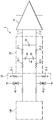
- the device 1 for acquiring signals from a sensor 100 comprising a differential amplifier 10, a filter circuit 20, a bias circuit 30, and a protection circuit 40.
- the differential amplifier 10 has a first input connected to a first line 11.1 and a second input connected to a second line 11.2.
- the first line 11.1 connects a first output of the sensor 100 to the first input of the amplifier 10 and the second line connects a second output of the sensor 100 to the second input of the amplifier 10.
- Amplifier 10 is of the “High Common Mode Range” type.
- the second terminal of the second capacitor 24 and the first terminal of the third capacitor 25 being connected together to ground.
- the polarization member 30 comprises a polarization resistor 31.1 connecting the first line 11.1 to the ground upstream of the second resistor 22.1 and a polarization resistor 31.1 connecting the second line to the ground upstream of the second resistance 22.2.
- the components 40.1, 40.2 are for example transient voltage suppression diodes of the Transil type which absorb the excess current to lower the voltage.
- the components 40.1, 40.2 are dimensioned to clip the lightning voltage to a value just necessary to respect the maximum voltages supported by the “high common mode range” amplifier and the filtering and polarization components of the assembly, that is to say according to the components used of the order of one hundred to three hundred volts.
- Lower clipping voltages would not make it possible to benefit from the reduction in the value of the parasitic currents and capacitance induced on the clipping components.
- Higher clipping voltages would require oversizing the filter components without benefiting from any significant additional reduction in these parasitic elements.
- the device may differ from that described, for example in terms of the number of components, as long as it meets the definition given in the claims.
- the components may have any maximum voltage after clipping between about 100 volts or so and about 300 volts.
- the maximum voltage may be between 150 volts and 200 volts, or even be equal to approximately 200 volts.
Landscapes
- Engineering & Computer Science (AREA)
- Power Engineering (AREA)
- Physics & Mathematics (AREA)
- General Physics & Mathematics (AREA)
- Amplifiers (AREA)
Description
La présente invention concerne le domaine des capteurs de mesure et plus précisément l'acquisition de signaux en provenance d'un capteur. Le capteur est par exemple un capteur de déplacement tel qu'un capteur passif de type LVDT (de l'anglais « Linear Variable Differential Transformer »).The present invention relates to the field of measurement sensors and more precisely to the acquisition of signals originating from a sensor. The sensor is for example a displacement sensor such as a passive sensor of LVDT type (standing for “Linear Variable Differential Transformer”).
Un dispositif d'acquisition de signaux d'un capteur, comprend généralement :
- un amplificateur différentiel standard ayant une première entrée reliée à une première ligne et une deuxième entrée reliée à une deuxième ligne, la première ligne et la deuxième ligne étant destinées à être reliées chacune à une sortie du capteur,
- un circuit de filtrage mode commun et mode différentiel relié à la première ligne et à la deuxième ligne,
- deux résistances de polarisation du capteur reliées respectivement à la première ligne et à la deuxième ligne.
- a standard differential amplifier having a first input connected to a first line and a second input connected to a second line, the first line and the second line being each intended to be connected to an output of the sensor,
- a common mode and differential mode filter circuit connected to the first line and to the second line,
- two polarization resistors of the sensor connected respectively to the first line and to the second line.
Les signaux fournis par les capteurs ont généralement une tension de quelques millivolts à quelques volts et l'amplificateur différentiel utilisé est un amplificateur standard adapté à traiter des signaux correspondant à ces tensions. Pour les applications dans lesquelles le capteur risque d'être frappé par la foudre, il existe actuellement deux solutions pour limiter le risque que la foudre n'entraîne une défaillance du dispositif d'acquisition.The signals supplied by the sensors generally have a voltage of a few millivolts to a few volts and the differential amplifier used is a standard amplifier suitable for processing signals corresponding to these voltages. For applications in which the sensor risks being struck by lightning, there are currently two solutions to limit the risk of lightning causing failure of the acquisition device.
La première solution consiste à dimensionner les composants du circuit de filtrage pour qu'ils supportent l'onde de foudre, la filtrent et limitent la tension et le courant en entrée de l'amplificateur à des niveaux que ce dernier puissent supporter, à savoir quelques volts ou dizaines de volts et quelques milliampères. Le circuit de filtrage comprend alors des impédances de plusieurs dizaines de kilohms pour réduire le courant en entrée de l'amplificateur. Du fait de ces impédances élevées, les capacités parasites de câblage et des composants du circuit ne sont plus négligeables et toute dissymétrie dans les valeurs de ces capacités parasites entre les deux lignes entraînent une dégradation importante des caractéristiques de rejection des perturbations de mode commun du montage. Par ailleurs les fréquences de coupure de filtrage nécessaires à l'atténuation des ondes de foudre est souvent difficile à accorder avec les besoins opérationnels. De plus, les composants du circuit de filtrage sont dimensionnés pour les hautes tensions, ce qui en augmente notablement le coût et la surface.The first solution consists in dimensioning the components of the filtering circuit so that they withstand the lightning wave, filter it and limit the voltage and the input current of the amplifier at levels that the latter can withstand, namely a few volts or tens of volts and a few milliamps. The filter circuit then includes impedances of several tens of kilohms to reduce the input current of the amplifier. Because of these high impedances, the parasitic capacitances of the wiring and of the components of the circuit are no longer negligible and any asymmetry in the values of these parasitic capacitances between the two lines leads to a significant degradation of the characteristics of rejection of the common mode disturbances of the assembly. . Furthermore, the filtering cutoff frequencies necessary for attenuating lightning waves are often difficult to match with operational requirements. In addition, the components of the filter circuit are sized for high voltages, which significantly increases the cost and area.
La deuxième solution consiste à relier à chacune des lignes, en amont des résistances de polarisation, des composants écrêteurs de tension capables de maintenir la tension en entrée du circuit de filtrage à une tension maximale de l'ordre de quelques volts à quelques dizaines de volts. Les composants écrêteurs sont par exemple des diodes de suppression de tensions transitoires de type Transil qui absorbent le courant excédentaire pour abaisser la tension. Les composants utilisés pour le circuit de filtrage sont alors des composants standards peu coûteux et perturbant relativement peu l'acquisition. En revanche, les composants écrêteurs, du fait de leurs courants de fuite et de leurs capacités parasites dégradent la précision de l'acquisition, perturbent les détections de pannes, dégradent le taux de réjection de mode commun si des impédances sont formées en amont, dégradent l'impédance d'entrée (du fait des courants de fuite dans le cas du courant continu et de capacités parasites dans le cas du courant alternatif). Enfin, les capacités parasites de ces composants écrêteurs peuvent induire des résonances en général inacceptables dans le circuit de mesure si le capteur présente une impédance inductive.The second solution consists in connecting to each of the lines, upstream of the polarization resistors, voltage limiter components capable of maintaining the voltage at the input of the filtering circuit at a maximum voltage of the order of a few volts to a few tens of volts. . The limiter components are for example transient voltage suppression diodes of the Transil type which absorb the excess current in order to lower the voltage. The components used for the filtering circuit are then inexpensive standard components and relatively little disturbing the acquisition. On the other hand, the limiter components, because of their leakage currents and their parasitic capacitances degrade the accuracy of the acquisition, disturb fault detection, degrade the common mode rejection rate if impedances are formed upstream, degrade input impedance (due to leakage currents in the case of direct current and capacitances interference in the case of alternating current). Finally, the parasitic capacitances of these clipping components can induce generally unacceptable resonances in the measurement circuit if the sensor has inductive impedance.
La deuxième solution est connue notamment du document
Un but de l'invention est de fournir un moyen pour protéger les dispositifs d'acquisition de mesure contre la foudre sans dégrader leurs performances.An aim of the invention is to provide a means for protecting the measurement acquisition devices against lightning without degrading their performance.
A cet effet, on prévoit, selon l'invention, un dispositif d'acquisition de signaux d'un capteur, comprenant :
- un amplificateur différentiel ayant une première entrée reliée à une première ligne et une deuxième entrée reliée à une deuxième ligne, la première ligne et la deuxième ligne étant destinées à être reliées chacune à une sortie du capteur,
- deux résistances de polarisation du dispositif de mesure reliées respectivement à la première ligne et à la deuxième ligne,
- un circuit de filtrage mode commun et mode différentiel relié à la première ligne et à la deuxième ligne,
- deux composants écrêteurs de foudre reliés respectivement à la première ligne et à la deuxième ligne.
- a differential amplifier having a first input connected to a first line and a second input connected to a second line, the first line and the second line being each intended to be connected to an output of the sensor,
- two polarization resistors of the measuring device connected respectively to the first line and to the second line,
- a common mode and differential mode filter circuit connected to the first line and to the second line,
- two lightning limiter components connected respectively to the first line and to the second line.
L'amplificateur différentiel est de type dit « High Common Mode Range » acceptant des tensions en entrée de plusieurs centaines de volts, généralement comprise entre environ 100 volts et 500 volts selon les fabricants et modèles. Un tel amplificateur opérationnel est choisi de telle manière que les composants écrêteurs soient dimensionnés pour écrêter la tension de foudre à cette valeur maximale. Le circuit de filtrage et les résistances de polarisation sont dimensionnés pour supporter la valeur maximale de tension écrêtée. Alors qu'un amplificateur différentiel de type classique aurait pû être choisi compte tenu des tensions à mesurer et des tensions en entrée du circuit, on choisit selon l'invention un amplificateur de type « High Common Mode Range » pour limiter l'écrêtage nécessaire en cas de foudroiement. En effet, en détournant l'amplificateur de type « High Common Mode Range » de son usage traditionnel, on crée un circuit d'acquisition, soumis au risque de foudre, autorisant en entrée de l'amplificateur une tension maximale de l'ordre d'une centaine de volts, ce qui permet de diminuer les énergies dissipées pendant l'écrêtage, et donc de diminuer la puissance de l'écrêtage. Ceci influe aussi, indirectement, favorablement sur les valeurs des éléments parasites des écrêteurs. En effet, les courants de fuite et la capacité parasite des composants écrêteurs sont proportionnels à la puissance des composants écrêteurs et inversement proportionnels à la tension d'écrêtage des composants écrêteurs. L'augmentation de leur tension d'écrêtage et la réduction de leur puissance permet de ramener ces courants et capacités parasites a des valeurs faibles qui ne dégradent plus les performances du montage. Les impédances et caractéristiques de filtrage mode commun et mode différentiel ne sont pas impactés par la présence des composants écrêteurs.The differential amplifier is of the so-called "High Common Mode Range" type accepting voltages in input of several hundred volts, generally between about 100 volts and 500 volts depending on the manufacturer and model. Such an operational amplifier is chosen such that the clipping components are dimensioned to clip the lightning voltage to this maximum value. The filter circuit and the bias resistors are sized to withstand the maximum value of clipped voltage. While a conventional type differential amplifier could have been chosen taking into account the voltages to be measured and the input voltages of the circuit, according to the invention an amplifier of the “High Common Mode Range” type is chosen to limit the clipping necessary in lightning strike. In fact, by diverting the “High Common Mode Range” type amplifier from its traditional use, an acquisition circuit is created, subject to the risk of lightning, allowing a maximum voltage of the order of d at the input of the amplifier. 'a hundred volts, which makes it possible to reduce the energies dissipated during clipping, and therefore to reduce the power of the clipping. This also influences, indirectly, favorably the values of the parasitic elements of the peakers. Indeed, the leakage currents and the parasitic capacitance of the clipping components are proportional to the power of the clipping components and inversely proportional to the clipping voltage of the clipping components. The increase in their clipping voltage and the reduction in their power makes it possible to reduce these parasitic currents and capacitances to low values which no longer degrade the performance of the assembly. The impedances and characteristics of common mode and differential mode filtering are not affected by the presence of the clipping components.
L'invention concerne également un procédé de protection contre la foudre d'un dispositif d'acquisition de signaux d'un capteur, le dispositif comprenant une première ligne et une deuxième ligne destinées à être reliées chacune à une sortie du capteur, deux résistances de polarisation du dispositif de mesure et deux composants écrêteurs de foudre étant reliés respectivement à la première ligne et à la deuxième ligne, et un circuit de filtrage mode commun et mode différentiel étant relié à la première ligne et à la deuxième ligne. Le procédé comprend les étapes de :
- utiliser, aux lieu et place d'un amplificateur différentiel classique, un amplificateur différentiel de type « High Common Mode Range » en reliant une première entrée de l'amplificateur différentiel à la première ligne et une deuxième entrée à la deuxième ligne,
- dimensionner les composants écrêteurs pour ramener une tension de foudre à une valeur maximale de tension de l'ordre de cent à trois cents volts, et le circuit de filtrage et les résistances de polarisation pour supporter la valeur maximale de tension.
- use, instead of a conventional differential amplifier, a differential amplifier of the “High Common Mode Range” type by connecting a first input of the differential amplifier to the first line and a second input to the second line,
- size the clipping components to reduce a lightning voltage to a maximum voltage value of the order of one hundred to three hundred volts, and the filter circuit and the bias resistors to withstand the maximum voltage value.
D'autres caractéristiques et avantages de l'invention ressortiront à la lecture de la description qui suit de modes de réalisation particuliers non limitatifs de l'invention.Other characteristics and advantages of the invention will emerge on reading the following description of particular non-limiting embodiments of the invention.
Il sera fait référence à la figure unique annexée représentant schématiquement le dispositif d'acquisition selon l'invention.Reference will be made to the single appended figure schematically showing the acquisition device according to the invention.
En référence à la figure, le dispositif 1 d'acquisition de signaux d'un capteur 100, comprenant un amplificateur différentiel 10, un circuit de filtrage 20, un circuit de polarisation 30, et un circuit de protection 40.Referring to the figure, the device 1 for acquiring signals from a
L'amplificateur différentiel 10 a une première entrée reliée à une première ligne 11.1 et une deuxième entrée reliée à une deuxième ligne 11.2. La première ligne 11.1 relie une première sortie du capteur 100 à la première entrée de l'amplificateur 10 et la deuxième ligne relie une deuxième sortie du capteur 100 à la deuxième entrée de l'amplificateur 10.The
L'amplificateur 10 est de type « High Common Mode Range ».
Le circuit de filtrage 20 est agencé pour assurer un filtrage en mode commun et mode différentiel pour réduire les perturbations de haute fréquence sans dégrader la précision des mesures dans la bande utile. Le circuit de filtrage 20 comprend :
- sur chacune de la première ligne 11.1 et la deuxième ligne 11.2, une première résistance 21.1, 21.2 reliée d'une part à l'amplificateur 10 et d'autre part à une deuxième résistance 22.1, 22.2 reliée à une entrée du dispositif d'acquisition 1,
- un
premier condensateur 23 reliant la première ligne 11.1 à la deuxième ligne 11.2 entre la première résistance 21.1, 21.2 et l'amplificateur 10, - un
deuxième condensateur 24 ayant une première borne reliée à la première ligne 11.1 entre la première résistance 21.1 et la deuxième résistance 22.1 et une deuxième borne reliée à une première borne d'untroisième condensateur 25 ayant une deuxième borne reliée à la deuxième ligne 11.2 entre la première résistance 21.2 et la deuxième résistance 22.2.
- on each of the first line 11.1 and the second line 11.2, a first resistor 21.1, 21.2 connected on the one hand to the
amplifier 10 and on the other hand to a second resistor 22.1, 22.2 connected to an input of the acquisition device 1, - a
first capacitor 23 connecting the first line 11.1 to the second line 11.2 between the first resistor 21.1, 21.2 and theamplifier 10, - a
second capacitor 24 having a first terminal connected to the first line 11.1 between the first resistor 21.1 and the second resistor 22.1 and a second terminal connected to a first terminal of athird capacitor 25 having a second terminal connected to the second line 11.2 between the first resistor 21.2 and the second resistor 22.2.
La deuxième borne du deuxième condensateur 24 et la première borne du troisième condensateur 25 étant reliées ensemble à la masse.The second terminal of the
L'organe de polarisation 30 comprend une résistance de polarisation 31.1 reliant la première ligne 11.1 à la masse en amont de la deuxième résistance 22.1 et une résistance de polarisation 31.1 reliant la deuxième ligne à la masse en amont de la deuxième résistance 22.2.The
Le circuit de protection 40 comprend :
- un composant 40.1 écrêteur de foudre reliant la première ligne 11.1 à la masse entre l'organe de
polarisation 30 et le capteur 100 ; - un composant 40.2 écrêteur de foudre reliant la deuxième ligne 11.2 à la masse entre l'organe de
polarisation 30 et le capteur 100.
- a lightning limiter component 40.1 connecting the first line 11.1 to ground between the
polarization member 30 and thesensor 100; - a lightning limiter component 40.2 connecting the second line 11.2 to ground between the
polarization member 30 and thesensor 100.
Les composants 40.1, 40.2 sont par exemple des diodes de suppression de tensions transitoires de type Transil qui absorbent le courant excédentaire pour abaisser la tension. Les composants 40.1, 40.2 sont dimensionnés pour écrêter la tension de foudre à une valeur juste nécessaire au respect des tensions maximales supportées par l'amplificateur « high common mode range » et les composants de filtrage et de polarisation du montage, soit selon les composants utilisés de l'ordre de cent à trois cents volts. Des tensions d'écrêtage plus faibles ne permettraient pas de bénéficier de la réduction de la valeur des courants et capacité parasites induites sur les composants écrêteurs. Des tensions d'écrêtages plus élevées nécessiteraient de sur-dimensionner les composants de filtrage sans pour autant bénéficier de réduction supplémentaires significatives de ces éléments parasites.The components 40.1, 40.2 are for example transient voltage suppression diodes of the Transil type which absorb the excess current to lower the voltage. The components 40.1, 40.2 are dimensioned to clip the lightning voltage to a value just necessary to respect the maximum voltages supported by the “high common mode range” amplifier and the filtering and polarization components of the assembly, that is to say according to the components used of the order of one hundred to three hundred volts. Lower clipping voltages would not make it possible to benefit from the reduction in the value of the parasitic currents and capacitance induced on the clipping components. Higher clipping voltages would require oversizing the filter components without benefiting from any significant additional reduction in these parasitic elements.
L'invention concerne ainsi également un procédé de protection contre la foudre d'un dispositif d'acquisition de signaux d'un capteur, le dispositif comprenant une première ligne et une deuxième ligne destinées à être reliées chacune à une sortie du capteur, deux résistances de polarisation du dispositif de mesure et deux composants écrêteurs de foudre étant reliés respectivement à la première ligne et à la deuxième ligne, et un circuit de filtrage mode commun et mode différentiel étant relié à la première ligne et à la deuxième ligne. Le procédé comprend les étapes de :
- utiliser, aux lieu et place d'un amplificateur différentiel classique, un amplificateur différentiel de type « High Common Mode Range » en reliant une première entrée de l'amplificateur différentiel à la première ligne et une deuxième entrée à la deuxième ligne,
- dimensionner les composants écrêteurs pour ramener une tension de foudre à une valeur maximale de tension de l'ordre de cent à trois cents volts, et le circuit de filtrage et les résistances de polarisation pour supporter la valeur maximale de tension.
- use, instead of a conventional differential amplifier, a differential amplifier of the “High Common Mode Range” type by connecting a first input of the differential amplifier to the first line and a second input to the second line,
- size the clipping components to reduce a lightning voltage to a maximum voltage value of the order of one hundred to three hundred volts, and the filter circuit and the bias resistors to withstand the maximum voltage value.
Bien entendu, l'invention n'est pas limitée aux modes de réalisation décrits mais englobe toute variante entrant dans le champ de l'invention telle que définie par les revendications.Of course, the invention is not limited to the embodiments described but encompasses any variant coming within the scope of the invention as defined by the claims.
En particulier, le dispositif peut présenter des différences par rapport à celui décrit, par exemple au niveau du nombre de composants, tant qu'il répond à la définition donnée dans les revendications.In particular, the device may differ from that described, for example in terms of the number of components, as long as it meets the definition given in the claims.
Il est possible de choisir les composants pour avoir n'importe quelle tension maximale après écrêtage entre environ 100 volts environ et 300 volts environ. La tension maximale peut être comprise entre 150 volts et 200 volts, voire être égale à 200 volts environ.It is possible to choose the components to have any maximum voltage after clipping between about 100 volts or so and about 300 volts. The maximum voltage may be between 150 volts and 200 volts, or even be equal to approximately 200 volts.
Claims (7)
- A device for acquiring signals from a sensor (100), comprising:· a differential amplifier (10) having a first input connected to a first line (11.1) and a second input connected to a second line(11.2), the first line and the second line each being for connection to a respective output of the sensor;· two bias resistors (31.1, 31.2) for biasing the measurement device and connected respectively to the first line and to the second line;· a common mode and differential mode filter circuit (20) connected to the first line and to the second line; and· two lightning limiter components (40.1, 40.2) connected respectively to the first line and to the second line;the device being characterized in that the differential amplifier is of the "high common mode range" type, in that the limiter components (40.1, 40.2) are dimensioned to reduce a lightning voltage to a maximum voltage value of about one hundred to three hundred volts, and in that the filter circuit (20) and the bias resistors (31.1, 31.2) are dimensioned to withstand the maximum voltage value.
- A device according to claim 1, wherein the filter circuit (20) comprises:· on each of the first line and the second line, a first resistor connected firstly to the amplifier and secondly a second resistor that is connected to a respective input of the acquisition device;· a first capacitor connecting the first line to the second line between the first resistor and the amplifier; and· a second capacitor having a first terminal connected to the first line between the first resistor and the second resistor and a second terminal connected to a first terminal of a third capacitor having a second terminal connected to the second line between the first resistor and the second resistor, the second terminal of the second capacitor and the first terminal of the third capacitor being connected to ground.
- A device according to claim 1 or claim 2, wherein the maximum voltage lies in the range approximately 150 volts to approximately 200 volts.
- A device according to claim 3, wherein the maximum voltage is approximately 200 volts.
- A method of providing lightning protection for a device (1) for acquiring signals from a sensor, the device comprising a first line (11.1) and a second line (11.2), each for connection to a respective output of the sensor, two bias resistors (31.1, 31.2) for biasing the measurement device and two lightning limiter components (40.1, 40.2) connected respectively to the first line and to the second line, and a common mode and differential mode filter circuit (20) connected to the first line and to the second line, characterized in that the method comprises the steps of:· using a differential amplifier (10) of "high common mode range" type, connecting a first input of the differential amplifier to the first line and a second input to the second line; and· dimensioning the limiter components (40.1, 40.2) to reduce a lightning voltage to a maximum voltage value of about one hundred to three hundred volts, and dimensioning the filter circuit (20) and the bias resistors (31.1, 31.2) to withstand that maximum voltage value.
- A device according to claim 5, wherein the maximum voltage lies in the range approximately 150 volts to approximately 200 volts.
- A device according to claim 6, wherein the maximum voltage is approximately 200 volts.
Applications Claiming Priority (2)
| Application Number | Priority Date | Filing Date | Title |
|---|---|---|---|
| FR1760358A FR3073283B1 (en) | 2017-11-03 | 2017-11-03 | IMPROVED LIGHTNING PROTECTION DEVICE FOR DIFFERENTIAL ENTRY |
| PCT/EP2018/080048 WO2019086625A1 (en) | 2017-11-03 | 2018-11-02 | Device and improved method for protecting against lightning for a differential input |
Publications (2)
| Publication Number | Publication Date |
|---|---|
| EP3704445A1 EP3704445A1 (en) | 2020-09-09 |
| EP3704445B1 true EP3704445B1 (en) | 2021-09-15 |
Family
ID=61599291
Family Applications (1)
| Application Number | Title | Priority Date | Filing Date |
|---|---|---|---|
| EP18799698.8A Active EP3704445B1 (en) | 2017-11-03 | 2018-11-02 | Device and improved method for protecting against lightning for a differential input |
Country Status (5)
| Country | Link |
|---|---|
| US (1) | US11088529B2 (en) |
| EP (1) | EP3704445B1 (en) |
| CN (1) | CN111295571B (en) |
| FR (1) | FR3073283B1 (en) |
| WO (1) | WO2019086625A1 (en) |
Families Citing this family (2)
| Publication number | Priority date | Publication date | Assignee | Title |
|---|---|---|---|---|
| US11879931B2 (en) * | 2021-08-25 | 2024-01-23 | Hamilton Sundstrand Corporation | Circuit testing and diagnosis |
| US11757281B2 (en) * | 2021-12-07 | 2023-09-12 | Infineon Technologies Ag | Electrostatic discharge protection device with integrated series resistors |
Family Cites Families (8)
| Publication number | Priority date | Publication date | Assignee | Title |
|---|---|---|---|---|
| US6816797B2 (en) * | 2000-09-29 | 2004-11-09 | Hydrogenics Corporation | System and method for measuring fuel cell voltage and high frequency resistance |
| KR100624365B1 (en) * | 2004-12-01 | 2006-09-18 | 주식회사 파워트론 | Battery cell voltage and internal impedance measuring circuit |
| JP5356418B2 (en) * | 2009-01-29 | 2013-12-04 | パナソニック株式会社 | Differential transmission circuit and electronic device including the same |
| FR2973873B1 (en) * | 2011-04-05 | 2013-05-10 | Sagem Defense Securite | METHOD FOR CORRECTING THE MEASUREMENT OF VOLTAGE AT THE TERMINALS OF A SENSOR |
| CN202886495U (en) * | 2012-10-17 | 2013-04-17 | 施杰 | Isolation-type signal testing and analyzing instrument |
| CN203759090U (en) * | 2014-03-14 | 2014-08-06 | 中国铁道科学研究院机车车辆研究所 | Current sampling circuit of rail-transit traction data acquisition system |
| CN204495459U (en) * | 2015-04-09 | 2015-07-22 | 梧州学院 | A kind of weighing data harvester |
| CN106405197B (en) * | 2016-11-25 | 2018-12-11 | 西安微电子技术研究所 | Flouride-resistani acid phesphatase 100V high precision electro current detection circuit |
-
2017
- 2017-11-03 FR FR1760358A patent/FR3073283B1/en active Active
-
2018
- 2018-11-02 WO PCT/EP2018/080048 patent/WO2019086625A1/en unknown
- 2018-11-02 EP EP18799698.8A patent/EP3704445B1/en active Active
- 2018-11-02 CN CN201880071295.8A patent/CN111295571B/en active Active
- 2018-11-02 US US16/761,434 patent/US11088529B2/en active Active
Also Published As
| Publication number | Publication date |
|---|---|
| CN111295571A (en) | 2020-06-16 |
| US11088529B2 (en) | 2021-08-10 |
| EP3704445A1 (en) | 2020-09-09 |
| US20200381912A1 (en) | 2020-12-03 |
| WO2019086625A1 (en) | 2019-05-09 |
| FR3073283A1 (en) | 2019-05-10 |
| CN111295571B (en) | 2021-08-27 |
| FR3073283B1 (en) | 2019-11-15 |
Similar Documents
| Publication | Publication Date | Title |
|---|---|---|
| EP3704445B1 (en) | Device and improved method for protecting against lightning for a differential input | |
| BE1023946B1 (en) | PARTICLE SENSOR IN A FLUID OF A LUBRICATION SYSTEM | |
| EP4127737B1 (en) | Rogowski current sensor which is fast and immune to voltage drifts | |
| EP0768533B1 (en) | Differential charge amplifier for piezoelectric sensor | |
| FR2827962A1 (en) | Hall effect current sensor is chip with opposite bias sensors and calibration circuits | |
| EP2830215B1 (en) | Load preamplifier | |
| EP1762854A2 (en) | Measuring device for very short current impulses | |
| FR2994776A1 (en) | ANALOGUE AMPLIFICATION DEVICE, IN PARTICULAR FOR A LASER ANEMOMETER | |
| EP4127736B1 (en) | Very-wide-bandwidth current sensor | |
| EP0086158B1 (en) | Supply circuit for an eddy current probe | |
| FR2930039A1 (en) | MAGNETIC FIELD MEASURING SYSTEM AND METHOD FOR REMOVING THE OFFSET OF A CORRESPONDING MAGNETIC FIELD SENSOR. | |
| CH692162A5 (en) | Measuring method for detecting a short circuit between turns of a coil integrated on a chip, and integrated circuit structure suitable for such a measuring method. | |
| FR2896882A1 (en) | ELECTROMAGNETIC DETECTOR FOR SPEED OF ROTATION OF ROTATING MEMBER | |
| EP2301164B1 (en) | System for transmitting an electrical signal, in particular frequency-related and radiation measurement device equipped with such a system | |
| WO2023052482A1 (en) | Active probe for measuring voltage at high impedances | |
| CH642205A5 (en) | AMPLIFIER CIRCUIT FOR MEASUREMENT PROBE. | |
| CH696895A5 (en) | Variable capacitor`s contact less measurement device, has electronic measurement circuit with resonant measurement circuit placed between transmission and triaxial cables, where transfer function of electronic circuit presents resonance | |
| WO2021104712A1 (en) | Noise reduction sensor for a motor vehicle | |
| WO2023174572A1 (en) | Magnetic field sensor for measuring a direct current | |
| WO2022069626A1 (en) | System and method for suppressing low-frequency magnetic noise from magneto-resistive sensors | |
| WO2002093687A1 (en) | Antenna quality factor self-adaptive device | |
| FR2919730A1 (en) | CURRENT SENSOR FOR MEASURING CURRENT CIRCULATING IN AT LEAST ONE DRIVER | |
| FR2941305A1 (en) | AMPLIFICATION STRUCTURE AND DETECTION AND MEASURING CHAIN COMPRISING SUCH A STRUCTURE. | |
| CH329786A (en) | Damping device for the oscillating member of an electromechanical device | |
| FR2788344A1 (en) | DEVICE FOR MEASURING A CURRENT FLOWING IN A CONDUCTOR |
Legal Events
| Date | Code | Title | Description |
|---|---|---|---|
| STAA | Information on the status of an ep patent application or granted ep patent |
Free format text: STATUS: UNKNOWN |
|
| STAA | Information on the status of an ep patent application or granted ep patent |
Free format text: STATUS: THE INTERNATIONAL PUBLICATION HAS BEEN MADE |
|
| PUAI | Public reference made under article 153(3) epc to a published international application that has entered the european phase |
Free format text: ORIGINAL CODE: 0009012 |
|
| STAA | Information on the status of an ep patent application or granted ep patent |
Free format text: STATUS: REQUEST FOR EXAMINATION WAS MADE |
|
| 17P | Request for examination filed |
Effective date: 20200429 |
|
| AK | Designated contracting states |
Kind code of ref document: A1 Designated state(s): AL AT BE BG CH CY CZ DE DK EE ES FI FR GB GR HR HU IE IS IT LI LT LU LV MC MK MT NL NO PL PT RO RS SE SI SK SM TR |
|
| AX | Request for extension of the european patent |
Extension state: BA ME |
|
| DAV | Request for validation of the european patent (deleted) | ||
| DAX | Request for extension of the european patent (deleted) | ||
| GRAP | Despatch of communication of intention to grant a patent |
Free format text: ORIGINAL CODE: EPIDOSNIGR1 |
|
| STAA | Information on the status of an ep patent application or granted ep patent |
Free format text: STATUS: GRANT OF PATENT IS INTENDED |
|
| INTG | Intention to grant announced |
Effective date: 20210323 |
|
| GRAS | Grant fee paid |
Free format text: ORIGINAL CODE: EPIDOSNIGR3 |
|
| GRAA | (expected) grant |
Free format text: ORIGINAL CODE: 0009210 |
|
| STAA | Information on the status of an ep patent application or granted ep patent |
Free format text: STATUS: THE PATENT HAS BEEN GRANTED |
|
| RIN1 | Information on inventor provided before grant (corrected) |
Inventor name: LE-MEUNIER, MATHIEU Inventor name: MELINE, OLIVIER |
|
| RAP3 | Party data changed (applicant data changed or rights of an application transferred) |
Owner name: SAFRAN ELECTRONICS & DEFENSE |
|
| AK | Designated contracting states |
Kind code of ref document: B1 Designated state(s): AL AT BE BG CH CY CZ DE DK EE ES FI FR GB GR HR HU IE IS IT LI LT LU LV MC MK MT NL NO PL PT RO RS SE SI SK SM TR |
|
| REG | Reference to a national code |
Ref country code: CH Ref legal event code: EP |
|
| REG | Reference to a national code |
Ref country code: DE Ref legal event code: R096 Ref document number: 602018023708 Country of ref document: DE |
|
| REG | Reference to a national code |
Ref country code: IE Ref legal event code: FG4D Free format text: LANGUAGE OF EP DOCUMENT: FRENCH |
|
| REG | Reference to a national code |
Ref country code: AT Ref legal event code: REF Ref document number: 1430839 Country of ref document: AT Kind code of ref document: T Effective date: 20211015 |
|
| REG | Reference to a national code |
Ref country code: LT Ref legal event code: MG9D |
|
| REG | Reference to a national code |
Ref country code: NL Ref legal event code: MP Effective date: 20210915 |
|
| PG25 | Lapsed in a contracting state [announced via postgrant information from national office to epo] |
Ref country code: HR Free format text: LAPSE BECAUSE OF FAILURE TO SUBMIT A TRANSLATION OF THE DESCRIPTION OR TO PAY THE FEE WITHIN THE PRESCRIBED TIME-LIMIT Effective date: 20210915 Ref country code: FI Free format text: LAPSE BECAUSE OF FAILURE TO SUBMIT A TRANSLATION OF THE DESCRIPTION OR TO PAY THE FEE WITHIN THE PRESCRIBED TIME-LIMIT Effective date: 20210915 Ref country code: RS Free format text: LAPSE BECAUSE OF FAILURE TO SUBMIT A TRANSLATION OF THE DESCRIPTION OR TO PAY THE FEE WITHIN THE PRESCRIBED TIME-LIMIT Effective date: 20210915 Ref country code: SE Free format text: LAPSE BECAUSE OF FAILURE TO SUBMIT A TRANSLATION OF THE DESCRIPTION OR TO PAY THE FEE WITHIN THE PRESCRIBED TIME-LIMIT Effective date: 20210915 Ref country code: BG Free format text: LAPSE BECAUSE OF FAILURE TO SUBMIT A TRANSLATION OF THE DESCRIPTION OR TO PAY THE FEE WITHIN THE PRESCRIBED TIME-LIMIT Effective date: 20211215 Ref country code: LT Free format text: LAPSE BECAUSE OF FAILURE TO SUBMIT A TRANSLATION OF THE DESCRIPTION OR TO PAY THE FEE WITHIN THE PRESCRIBED TIME-LIMIT Effective date: 20210915 Ref country code: NO Free format text: LAPSE BECAUSE OF FAILURE TO SUBMIT A TRANSLATION OF THE DESCRIPTION OR TO PAY THE FEE WITHIN THE PRESCRIBED TIME-LIMIT Effective date: 20211215 |
|
| REG | Reference to a national code |
Ref country code: AT Ref legal event code: MK05 Ref document number: 1430839 Country of ref document: AT Kind code of ref document: T Effective date: 20210915 |
|
| PG25 | Lapsed in a contracting state [announced via postgrant information from national office to epo] |
Ref country code: LV Free format text: LAPSE BECAUSE OF FAILURE TO SUBMIT A TRANSLATION OF THE DESCRIPTION OR TO PAY THE FEE WITHIN THE PRESCRIBED TIME-LIMIT Effective date: 20210915 Ref country code: GR Free format text: LAPSE BECAUSE OF FAILURE TO SUBMIT A TRANSLATION OF THE DESCRIPTION OR TO PAY THE FEE WITHIN THE PRESCRIBED TIME-LIMIT Effective date: 20211216 |
|
| PG25 | Lapsed in a contracting state [announced via postgrant information from national office to epo] |
Ref country code: AT Free format text: LAPSE BECAUSE OF FAILURE TO SUBMIT A TRANSLATION OF THE DESCRIPTION OR TO PAY THE FEE WITHIN THE PRESCRIBED TIME-LIMIT Effective date: 20210915 |
|
| PG25 | Lapsed in a contracting state [announced via postgrant information from national office to epo] |
Ref country code: IS Free format text: LAPSE BECAUSE OF FAILURE TO SUBMIT A TRANSLATION OF THE DESCRIPTION OR TO PAY THE FEE WITHIN THE PRESCRIBED TIME-LIMIT Effective date: 20220115 Ref country code: SM Free format text: LAPSE BECAUSE OF FAILURE TO SUBMIT A TRANSLATION OF THE DESCRIPTION OR TO PAY THE FEE WITHIN THE PRESCRIBED TIME-LIMIT Effective date: 20210915 Ref country code: SK Free format text: LAPSE BECAUSE OF FAILURE TO SUBMIT A TRANSLATION OF THE DESCRIPTION OR TO PAY THE FEE WITHIN THE PRESCRIBED TIME-LIMIT Effective date: 20210915 Ref country code: RO Free format text: LAPSE BECAUSE OF FAILURE TO SUBMIT A TRANSLATION OF THE DESCRIPTION OR TO PAY THE FEE WITHIN THE PRESCRIBED TIME-LIMIT Effective date: 20210915 Ref country code: PT Free format text: LAPSE BECAUSE OF FAILURE TO SUBMIT A TRANSLATION OF THE DESCRIPTION OR TO PAY THE FEE WITHIN THE PRESCRIBED TIME-LIMIT Effective date: 20220117 Ref country code: PL Free format text: LAPSE BECAUSE OF FAILURE TO SUBMIT A TRANSLATION OF THE DESCRIPTION OR TO PAY THE FEE WITHIN THE PRESCRIBED TIME-LIMIT Effective date: 20210915 Ref country code: NL Free format text: LAPSE BECAUSE OF FAILURE TO SUBMIT A TRANSLATION OF THE DESCRIPTION OR TO PAY THE FEE WITHIN THE PRESCRIBED TIME-LIMIT Effective date: 20210915 Ref country code: ES Free format text: LAPSE BECAUSE OF FAILURE TO SUBMIT A TRANSLATION OF THE DESCRIPTION OR TO PAY THE FEE WITHIN THE PRESCRIBED TIME-LIMIT Effective date: 20210915 Ref country code: EE Free format text: LAPSE BECAUSE OF FAILURE TO SUBMIT A TRANSLATION OF THE DESCRIPTION OR TO PAY THE FEE WITHIN THE PRESCRIBED TIME-LIMIT Effective date: 20210915 Ref country code: CZ Free format text: LAPSE BECAUSE OF FAILURE TO SUBMIT A TRANSLATION OF THE DESCRIPTION OR TO PAY THE FEE WITHIN THE PRESCRIBED TIME-LIMIT Effective date: 20210915 Ref country code: AL Free format text: LAPSE BECAUSE OF FAILURE TO SUBMIT A TRANSLATION OF THE DESCRIPTION OR TO PAY THE FEE WITHIN THE PRESCRIBED TIME-LIMIT Effective date: 20210915 |
|
| REG | Reference to a national code |
Ref country code: DE Ref legal event code: R097 Ref document number: 602018023708 Country of ref document: DE |
|
| PG25 | Lapsed in a contracting state [announced via postgrant information from national office to epo] |
Ref country code: MC Free format text: LAPSE BECAUSE OF FAILURE TO SUBMIT A TRANSLATION OF THE DESCRIPTION OR TO PAY THE FEE WITHIN THE PRESCRIBED TIME-LIMIT Effective date: 20210915 |
|
| REG | Reference to a national code |
Ref country code: CH Ref legal event code: PL |
|
| PLBE | No opposition filed within time limit |
Free format text: ORIGINAL CODE: 0009261 |
|
| STAA | Information on the status of an ep patent application or granted ep patent |
Free format text: STATUS: NO OPPOSITION FILED WITHIN TIME LIMIT |
|
| PG25 | Lapsed in a contracting state [announced via postgrant information from national office to epo] |
Ref country code: LU Free format text: LAPSE BECAUSE OF NON-PAYMENT OF DUE FEES Effective date: 20211102 Ref country code: DK Free format text: LAPSE BECAUSE OF FAILURE TO SUBMIT A TRANSLATION OF THE DESCRIPTION OR TO PAY THE FEE WITHIN THE PRESCRIBED TIME-LIMIT Effective date: 20210915 Ref country code: BE Free format text: LAPSE BECAUSE OF NON-PAYMENT OF DUE FEES Effective date: 20211130 |
|
| REG | Reference to a national code |
Ref country code: BE Ref legal event code: MM Effective date: 20211130 |
|
| 26N | No opposition filed |
Effective date: 20220616 |
|
| PG25 | Lapsed in a contracting state [announced via postgrant information from national office to epo] |
Ref country code: SI Free format text: LAPSE BECAUSE OF FAILURE TO SUBMIT A TRANSLATION OF THE DESCRIPTION OR TO PAY THE FEE WITHIN THE PRESCRIBED TIME-LIMIT Effective date: 20210915 |
|
| PG25 | Lapsed in a contracting state [announced via postgrant information from national office to epo] |
Ref country code: IE Free format text: LAPSE BECAUSE OF NON-PAYMENT OF DUE FEES Effective date: 20211102 |
|
| PG25 | Lapsed in a contracting state [announced via postgrant information from national office to epo] |
Ref country code: IT Free format text: LAPSE BECAUSE OF FAILURE TO SUBMIT A TRANSLATION OF THE DESCRIPTION OR TO PAY THE FEE WITHIN THE PRESCRIBED TIME-LIMIT Effective date: 20210915 |
|
| PG25 | Lapsed in a contracting state [announced via postgrant information from national office to epo] |
Ref country code: CY Free format text: LAPSE BECAUSE OF FAILURE TO SUBMIT A TRANSLATION OF THE DESCRIPTION OR TO PAY THE FEE WITHIN THE PRESCRIBED TIME-LIMIT Effective date: 20210915 |
|
| PG25 | Lapsed in a contracting state [announced via postgrant information from national office to epo] |
Ref country code: LI Free format text: LAPSE BECAUSE OF NON-PAYMENT OF DUE FEES Effective date: 20220630 Ref country code: HU Free format text: LAPSE BECAUSE OF FAILURE TO SUBMIT A TRANSLATION OF THE DESCRIPTION OR TO PAY THE FEE WITHIN THE PRESCRIBED TIME-LIMIT; INVALID AB INITIO Effective date: 20181102 Ref country code: CH Free format text: LAPSE BECAUSE OF NON-PAYMENT OF DUE FEES Effective date: 20220630 |
|
| PGFP | Annual fee paid to national office [announced via postgrant information from national office to epo] |
Ref country code: GB Payment date: 20231019 Year of fee payment: 6 |
|
| PGFP | Annual fee paid to national office [announced via postgrant information from national office to epo] |
Ref country code: FR Payment date: 20231019 Year of fee payment: 6 Ref country code: DE Payment date: 20231019 Year of fee payment: 6 |
|
| PG25 | Lapsed in a contracting state [announced via postgrant information from national office to epo] |
Ref country code: MK Free format text: LAPSE BECAUSE OF FAILURE TO SUBMIT A TRANSLATION OF THE DESCRIPTION OR TO PAY THE FEE WITHIN THE PRESCRIBED TIME-LIMIT Effective date: 20210915 |