EP3702123A1 - Injection molded article - Google Patents
Injection molded article Download PDFInfo
- Publication number
- EP3702123A1 EP3702123A1 EP18888242.7A EP18888242A EP3702123A1 EP 3702123 A1 EP3702123 A1 EP 3702123A1 EP 18888242 A EP18888242 A EP 18888242A EP 3702123 A1 EP3702123 A1 EP 3702123A1
- Authority
- EP
- European Patent Office
- Prior art keywords
- region
- molded article
- injection molded
- base
- mold
- Prior art date
- Legal status (The legal status is an assumption and is not a legal conclusion. Google has not performed a legal analysis and makes no representation as to the accuracy of the status listed.)
- Granted
Links
Images



Classifications
-
- B—PERFORMING OPERATIONS; TRANSPORTING
- B29—WORKING OF PLASTICS; WORKING OF SUBSTANCES IN A PLASTIC STATE IN GENERAL
- B29C—SHAPING OR JOINING OF PLASTICS; SHAPING OF MATERIAL IN A PLASTIC STATE, NOT OTHERWISE PROVIDED FOR; AFTER-TREATMENT OF THE SHAPED PRODUCTS, e.g. REPAIRING
- B29C45/00—Injection moulding, i.e. forcing the required volume of moulding material through a nozzle into a closed mould; Apparatus therefor
- B29C45/0025—Preventing defects on the moulded article, e.g. weld lines, shrinkage marks
-
- B—PERFORMING OPERATIONS; TRANSPORTING
- B29—WORKING OF PLASTICS; WORKING OF SUBSTANCES IN A PLASTIC STATE IN GENERAL
- B29C—SHAPING OR JOINING OF PLASTICS; SHAPING OF MATERIAL IN A PLASTIC STATE, NOT OTHERWISE PROVIDED FOR; AFTER-TREATMENT OF THE SHAPED PRODUCTS, e.g. REPAIRING
- B29C45/00—Injection moulding, i.e. forcing the required volume of moulding material through a nozzle into a closed mould; Apparatus therefor
- B29C45/17—Component parts, details or accessories; Auxiliary operations
- B29C45/26—Moulds
- B29C45/27—Sprue channels ; Runner channels or runner nozzles
- B29C45/2701—Details not specific to hot or cold runner channels
- B29C45/2708—Gates
-
- B—PERFORMING OPERATIONS; TRANSPORTING
- B01—PHYSICAL OR CHEMICAL PROCESSES OR APPARATUS IN GENERAL
- B01L—CHEMICAL OR PHYSICAL LABORATORY APPARATUS FOR GENERAL USE
- B01L3/00—Containers or dishes for laboratory use, e.g. laboratory glassware; Droppers
- B01L3/50—Containers for the purpose of retaining a material to be analysed, e.g. test tubes
- B01L3/502—Containers for the purpose of retaining a material to be analysed, e.g. test tubes with fluid transport, e.g. in multi-compartment structures
- B01L3/5027—Containers for the purpose of retaining a material to be analysed, e.g. test tubes with fluid transport, e.g. in multi-compartment structures by integrated microfluidic structures, i.e. dimensions of channels and chambers are such that surface tension forces are important, e.g. lab-on-a-chip
-
- B—PERFORMING OPERATIONS; TRANSPORTING
- B29—WORKING OF PLASTICS; WORKING OF SUBSTANCES IN A PLASTIC STATE IN GENERAL
- B29C—SHAPING OR JOINING OF PLASTICS; SHAPING OF MATERIAL IN A PLASTIC STATE, NOT OTHERWISE PROVIDED FOR; AFTER-TREATMENT OF THE SHAPED PRODUCTS, e.g. REPAIRING
- B29C33/00—Moulds or cores; Details thereof or accessories therefor
- B29C33/42—Moulds or cores; Details thereof or accessories therefor characterised by the shape of the moulding surface, e.g. ribs or grooves
-
- B—PERFORMING OPERATIONS; TRANSPORTING
- B29—WORKING OF PLASTICS; WORKING OF SUBSTANCES IN A PLASTIC STATE IN GENERAL
- B29C—SHAPING OR JOINING OF PLASTICS; SHAPING OF MATERIAL IN A PLASTIC STATE, NOT OTHERWISE PROVIDED FOR; AFTER-TREATMENT OF THE SHAPED PRODUCTS, e.g. REPAIRING
- B29C45/00—Injection moulding, i.e. forcing the required volume of moulding material through a nozzle into a closed mould; Apparatus therefor
- B29C45/0046—Details relating to the filling pattern or flow paths or flow characteristics of moulding material in the mould cavity
-
- B—PERFORMING OPERATIONS; TRANSPORTING
- B29—WORKING OF PLASTICS; WORKING OF SUBSTANCES IN A PLASTIC STATE IN GENERAL
- B29C—SHAPING OR JOINING OF PLASTICS; SHAPING OF MATERIAL IN A PLASTIC STATE, NOT OTHERWISE PROVIDED FOR; AFTER-TREATMENT OF THE SHAPED PRODUCTS, e.g. REPAIRING
- B29C45/00—Injection moulding, i.e. forcing the required volume of moulding material through a nozzle into a closed mould; Apparatus therefor
- B29C45/17—Component parts, details or accessories; Auxiliary operations
- B29C45/26—Moulds
- B29C45/2628—Moulds with mould parts forming holes in or through the moulded article, e.g. for bearing cages
-
- B—PERFORMING OPERATIONS; TRANSPORTING
- B29—WORKING OF PLASTICS; WORKING OF SUBSTANCES IN A PLASTIC STATE IN GENERAL
- B29C—SHAPING OR JOINING OF PLASTICS; SHAPING OF MATERIAL IN A PLASTIC STATE, NOT OTHERWISE PROVIDED FOR; AFTER-TREATMENT OF THE SHAPED PRODUCTS, e.g. REPAIRING
- B29C45/00—Injection moulding, i.e. forcing the required volume of moulding material through a nozzle into a closed mould; Apparatus therefor
- B29C45/17—Component parts, details or accessories; Auxiliary operations
- B29C45/26—Moulds
- B29C45/263—Moulds with mould wall parts provided with fine grooves or impressions, e.g. for record discs
-
- B—PERFORMING OPERATIONS; TRANSPORTING
- B29—WORKING OF PLASTICS; WORKING OF SUBSTANCES IN A PLASTIC STATE IN GENERAL
- B29C—SHAPING OR JOINING OF PLASTICS; SHAPING OF MATERIAL IN A PLASTIC STATE, NOT OTHERWISE PROVIDED FOR; AFTER-TREATMENT OF THE SHAPED PRODUCTS, e.g. REPAIRING
- B29C33/00—Moulds or cores; Details thereof or accessories therefor
- B29C33/42—Moulds or cores; Details thereof or accessories therefor characterised by the shape of the moulding surface, e.g. ribs or grooves
- B29C2033/422—Moulding surfaces provided with a shape to promote flow of material in the mould cavity
-
- B—PERFORMING OPERATIONS; TRANSPORTING
- B29—WORKING OF PLASTICS; WORKING OF SUBSTANCES IN A PLASTIC STATE IN GENERAL
- B29C—SHAPING OR JOINING OF PLASTICS; SHAPING OF MATERIAL IN A PLASTIC STATE, NOT OTHERWISE PROVIDED FOR; AFTER-TREATMENT OF THE SHAPED PRODUCTS, e.g. REPAIRING
- B29C45/00—Injection moulding, i.e. forcing the required volume of moulding material through a nozzle into a closed mould; Apparatus therefor
- B29C45/0025—Preventing defects on the moulded article, e.g. weld lines, shrinkage marks
- B29C2045/0043—Preventing defects on the moulded article, e.g. weld lines, shrinkage marks preventing shrinkage by reducing the wall thickness of the moulded article
-
- G—PHYSICS
- G01—MEASURING; TESTING
- G01N—INVESTIGATING OR ANALYSING MATERIALS BY DETERMINING THEIR CHEMICAL OR PHYSICAL PROPERTIES
- G01N33/00—Investigating or analysing materials by specific methods not covered by groups G01N1/00 - G01N31/00
- G01N33/48—Biological material, e.g. blood, urine; Haemocytometers
- G01N33/50—Chemical analysis of biological material, e.g. blood, urine; Testing involving biospecific ligand binding methods; Immunological testing
- G01N33/53—Immunoassay; Biospecific binding assay; Materials therefor
- G01N33/5302—Apparatus specially adapted for immunological test procedures
Definitions
- the present invention relates to an injection molded article that has a plurality of protrusions, so-called bosses and ribs, with different inner diameters on its substrate, and that is formed by injection molding involving separating the plurality of protrusions from a mold.
- a sink mark is formed, for example, on the surface of a portion where the thickness of the product greatly varies.
- a sink mark is caused by the following reason. A molten thermoplastic shrinks while being cooled and solidified in a mold. In this process, a portion with a greater thickness than the neighboring portion is cooled more slowly, and therefore solidifies and shrinks after the neighboring portion solidifies.
- the core-side portion in the fixed mold defining the product visible portion of a plastic product is generally flat and more quickly cooled than the cavity-side portion in the movable mold having complicated structures such as a boss and a rib. Therefore, the core-side portion in the fixed mold is separated from the mold earlier than the cavity-side portion in the movable mold including the project invisible portion, and causes post-shrinkage, which is likely to result in a sink mark.
- a sink mark is a recessed depression on the surface of a product. Sink marks not only reduce the visual quality of the product and lower the value, but also prevent uniform painting and impair the appearance. This may increase the repair cost.
- Patent Document 1 JP H6-315955 A
- the product visible surface of a component of a micro fluid chip is required to prevent leakage of liquid and achieve the accuracy in height of a flow channel for fluid when an optical component is joined thereto. This is because the flow channel is formed by joining the optical component thereto.
- An object of the present invention is to provide an injection molded article that can prevent leakage of liquid and achieve the required accuracy in height of a flow channel.
- an invention recited in claim 1 is an injection molded article that is obtained by injection molding a molten resin into a mold, the injection molded article including:
- the invention recited in claim 2 is the injection molded article according to claim 1, wherein the thickness of the thickest portion is two or more times greater than the plate thickness of the base.
- the invention recited in claim 3 is the injection molded article according to claim 1 or 2, wherein the surface roughness of the processed region is 1 to 2 ⁇ m in Ra.
- the invention recited in claim 4 is the injection molded article according to any one of claims 1 to 3, wherein when an area of a smallest circle containing the projected region is defined as 100%, the injection molded article is obtained from the mold roughened to make a surface roughness greater than the surface roughness of the mirror surface region, in an area that is within the smallest circle and is 50 to 100% of an area of the smallest circle.
- the invention recited in claim 5 is the injection molded article according to any one of claims 1 to 4, wherein a region where a surface accuracy of the mold is not achieved is formed in a region where a region of the thickest portion is projected on an invisible surface defining a surface other than the base.
- the invention recited in claim 6 is the injection molded article according to any one of claims 1 to 5, wherein the mirror surface region is included in a region where a region having a thickness value of 70 to 95% is projected on the base.
- a test chip 10 is a chip (micro fluid chip) used for test, analysis, and so on of a biological material based on an antigen-antibody reaction. As illustrated in FIGS. 1 and 2 , the test chip 10 includes a test chip substrate 12, a first protrusion 13, and a second protrusion 14.
- the test chip substrate 12 is made of a resin.
- the requirements for the resin are high formability (transformability and releasability), high transparency, and low self-fluorescence with respect to the ultraviolet ray and visible ray.
- the test chip substrate 12 has a flow channel 11 through which liquid or the like injected by a non-illustrated liquid feeder flows.
- the test chip substrate 12 includes a first substrate (base) 12a as a thin plate-shaped member, a flow channel seal (not illustrated), and a second substrate 12b (optical component such as a prism).
- the flow channel 11 is formed in a region defined by the first substrate 12a and the second substrate 12b attached together with a flow channel seal.
- the first substrate 12a and the second substrate 12b of the test chip substrate 12 are manufactured by a method such as injection molding, press molding, and machine processing. At least one of the first substrate 12a and the second substrate 12b may be microfabricated.
- the first substrate 12a has a gate GA.
- the gate GA serves as an inlet when injecting a resin material into the mold.
- the gate GA has a bridging function for filling the cavity with the resin material injected through a sprue.
- the test chip substrate 12 is formed by joining the first substrate 12a and the second substrate 12b. When the first substrate 12a and the second substrate 12b are joined, the flow channel 11 is formed therebetween.
- the substrates may be joined by a welding method that joins resin-made substrates by heating them using a heat plate, hot air, a heating roller, ultrasonic wave, vibration, laser, double-sided seal, or the like, a bonding method that joins resin-made substrates using adhesive or solution, a method that joins resin-made substrates utilizing their own adhesiveness, or a method that joins substrates by applying surface treatment such as plasma treatment to resin-made substrates. In this manner, the test chip 10 having the flow channel 11 therein is manufactured.
- the flow channel 11 includes a reaction channel 15 extending in a predetermined direction (direction along an upper surface 12c of the test chip substrate 12 in FIG. 2 ) inside the test chip substrate 12, a communication channel 16 for communication between the reaction channel 15 and the first protrusion 13, and a communication channel 17 for communication between the reaction channel 15 and the second protrusion 14.
- a groove for a flow channel (a part corresponding to the reaction channel 15 in FIG. 2 ) is formed in the second substrate 12b. Then, the first substrate 12a serving as a cover is joined to the second substrate 12b having the flow channel groove, in a manner such that the flow channel groove faces inward. In this way, the flow channel 11 is formed.
- the flow channel i i may be formed by joining the first substrate 12a and the second substrate 12b, in a manner such that a double-sided seal having the flow channel 11 is interposed therebetween.
- the plate thickness of the second substrate 12b having the flow channel groove is preferably 0.2 mm to 5 mm, more preferably 0.5 mm to 2 mm.
- the plate thickness of the first substrate 12a serving as a lid (cover) for the flow channel groove is preferably 0.2 mm to 5 mm, more preferably 0.5 mm to 2 mm, taking into account the formability.
- the test chip substrate 12 is made of a low-cost, disposable resin, specifically a thermoplastic resin.
- thermoplastic resins are polycarbonate, polymethylmethacrylate, polystyrene, polyacrylonitrile, polyvinyl chloride, polyethylene terephthalate, nylon 6, nylon 66, polyvinyl acetate, polyvinylidene chloride, polypropylene, polypropylene, polyisoprene, polyethylene, polydimethylsiloxane, and cyclic polyolefin.
- Particularly preferred examples are polymethylmethacrylate and cyclic polyolefin.
- the first protrusion 13 is integrally formed on the upper surface of the test chip substrate 12 (first substrate 12a).
- the first protrusion 13 has an inner diameter portion 21, and serves as a reagent mixer and a reagent reactor for mixing and reacting a reagent in the inner diameter portion 21. Techniques for mixing and reacting a reagent are well known in the art, and will not be described herein.
- the inner diameter portion 21 communicates with the communication channel 16 of the flow channel 11.
- the second protrusion 14 is integrally formed on the upper surface of the test chip substrate 12, but in a region different from the region where the first protrusion 13 is formed.
- the second protrusion 14 has an inner diameter portion 22.
- the inner diameter portion 22 communicates with the communication channel 17 of the flow channel 11.
- the first protrusion 13 and the second protrusion 14 respectively have holes 13a and 14a each extending through the first substrate 12a.
- the holes 13a and 14a in the respective protrusions (first protrusion 13 and second protrusion 14) are connected through another component (second substrate 12b) to form the flow channel 11.
- Each of the first protrusion 13 and the second protrusion 14 is formed to have a thickness greater than a plate thickness of the first substrate 12a.
- the thickness of the thickest portion of the protrusions is two or more times greater than the plate thickness of the first substrate 12a.
- the thickest portion of the protrusions is the center of a sphere BA that is the largest imaginary sphere located inside the injection molded article (inside the first protrusion 13 in the present embodiment) and tangent to the wall surface thereof.
- the thickest portion of the protrusion can be calculated with, for example, the maximum ball algorithm used in 3D shape analysis software.
- a processed region processed to have a surface roughness greater (by several nanometers to several tens of nanometers in Ra) than the surface roughness of a mirror surface region E2 including a region between the holes 13a and 14a on the first substrate 12a is formed in a projected region E1 (that is, a region where a perpendicular line is drawn from a region having a thickness value of 95 to 100% to the first substrate 12a) where a region having a thickness value of 95 to 100% is projected on the first substrate 12a.
- the surface roughness of the processed region is 1 to 2 ⁇ m in Ra (arithmetic average roughness).
- the injection molded article of the present invention is the test chip 10 excluding the second substrate 12b that is an optical component.
- the projected region E1 is circular, and the projected region E1 and the smallest circle C1 exactly coincide.
- the present invention is not limited thereto. That is, the projected region E1 is not always circular, and hence the projected region E1 and the smallest circle C1 do not always coincide.
- the processed region E3 is not always circular, and may have any shape as long as its area is in the range of 50 to 100% of the area of the smallest circle C1.
- the injection molded article of the present invention is obtained by injection molding a molten resin into a mold that is processed such that the mirror surface region E2 and the projected region E1 are located close to each other.
- the mirror surface region E2 is included in a region E4 (a region adjacent to the projected region E1) where a region having a thickness value of 70 to 95% is projected on the first substrate 12a. That is, the mirror surface E2 is located close to the projected region E1 where sink marks are likely to be formed.
- sink marks are likely to be formed.
- roughening cannot be applied to the mirror surface region E2 because flatness and specularity are required there. Accordingly, in the present embodiment, roughening is applied to the region close to the mirror surface region E2.
- the present invention even when the region (projected region E1) where sink marks are likely to be formed and the region (mirror surface region E2) requiring flatness and specularity are close to each other, formation of sink marks on the visible surface of the first substrate 12a is prevented.
- FIG. 7 is a schematic diagram illustrating a so-called "mold clamping step” for forming a cavity by clamping two molds (movable mold 31 and fixed mold 32).
- FIG. 8 is a schematic diagram illustrating a so-called "ejection step” for removing an injection molded article 40 from the injection mold 30.
- the injection mold 30 includes the movable mold 31 with a recess (cavity) 310 in the shape of the injection molded article 40, the fixed mold 32 against which the movable mold 31 is pressed so as to close the recess 310, an ejector pin 33 that pushes the injection molded article 40 outward (in the direction of the arrow X in FIG. 8 ), an ejector member 34, core pins 35 each defining the internal shape of a protrusion, and a cylinder unit 36 that supplies a resin material (not illustrated) as the material of the injection molded article 40 to the cavity.
- the injection molding process includes a mold clamping step, an injection step, a pressure holding step, a cooling step, a mold opening step, and an ejection step. Injection molding is performed in this order.
- the mold clamping step the movable mold 31 and the fixed mold 32 are clamped together to close the recess 310 formed in the movable mold 31, thereby forming a cavity.
- a resin material molten resin
- the resin material flows through a sprue SP (unwanted portion of the injection molded article 40) and the gate GA, and is filled in the cavity.
- the resin material When filled in the cavity of the mold, the resin material is cooled and shrinks in the mold. Since the shrinkage causes a change in the volume, this shrinkage action results in a dimensional change of a molded article, a shape transfer failure, and the like. To prevent these issues, the volume of resin reduced due to the shrinkage is compensated for by applying a holding pressure on the molding machine side (pressure holding step). Then, the resin material is cooled in the mold until its temperature decreases to a level at which it can be extracted from the mold (cooling step).
- the movable mold 31 is separated from the fixed mold 32 (mold opening step) as illustrated in FIG. 8 .
- the molded article comes with the movable mold 31.
- the injection molded article 40 is demolded (ejection step).
- the second substrate 12b is joined to the injection molded article 40 to obtain a test chip 10.
- the predetermined region (the region corresponding to the processed region of the first substrate 12a) of the surface of the fixed mold 32 is roughened (sandblasted)
- resin is not easily separated from the fixed mold 32 during cooling and shrinkage. This prevents formation of sink marks on the visible surface of the injection molded article 40 (first substrate 12a).
- test chip substrate 12 first substrate 12a
- Comparative Examples 1 to 3 of the test chip substrate 12 (first substrate 12a) according to the present invention will be described with reference to FIG. 9 .
- a test chip substrate 12 of Comparative Example 1 is configured such that the plate thickness of a first substrate 12a (base plate thickness) is 1.3 mm, and the thickness value of the thickest portion of the first substrate 12a is 4.2 mm.
- the area of a smallest circle C1 containing a projected region E1 is 1.4n mm 2 ; the area of a processed region E3 is 1 ⁇ mm 2 ; and the ratio (percentage) of the area of a processed region E3 to the area of the smallest circle C1 is 71%.
- the surface roughness of the processed region E3 is 0.5 ⁇ m in Ra.
- a test chip substrate 12 of Comparative Example 2 is configured such that the plate thickness of a first substrate 12a (base plate thickness) is 1.3 mm, and the thickness value of the thickest portion of the first substrate 12a is 4.2 mm.
- the area of a smallest circle C1 containing a projected region E1 is 1.4 ⁇ mm 2 ; the area of a processed region E3 is 1 ⁇ mm 2 ; and the ratio (percentage) of the area of a processed region E3 to the area of the smallest circle C1 is 71%.
- the surface roughness of the processed region E3 is 3 ⁇ m in Ra.
- a test chip substrate 12 of Comparative Example 3 is configured such that the plate thickness of a first substrate 12a (base plate thickness) is 1.3 mm, and the thickness value of the thickest portion of the first substrate 12a is 4.2 mm.
- the area of a smallest circle C1 containing a projected region E1 is 1.4 ⁇ mm 2 ; the area of a processed region E3 is 0.5 ⁇ mm 2 ; and the ratio (percentage) of the area of a processed region E3 to the area of the smallest circle C1 is 36%.
- the surface roughness of the processed region E3 is 1 ⁇ m in Ra.
- a test chip substrate 12 of Example 1 is configured such that the plate thickness of a first substrate 12a (base plate thickness) is 1.3 mm, and the thickness value of the thickest portion of the first substrate 12a is 4.2 mm.
- the area of a smallest circle C1 containing a projected region E1 is 1.4 ⁇ mm 2 ; the area of a processed region E3 is 1 ⁇ mm 2 ; and the ratio (percentage) of the area of a processed region E3 to the area of the smallest circle C1 is 71 %.
- the surface roughness of the processed region E3 is 1 ⁇ m in Ra.
- a test chip substrate 12 of Example 2 is configured such that the plate thickness of a first substrate 12a (base plate thickness) is 1.3 mm, and the thickness value of the thickest portion of the first substrate 12a is 4.2 mm.
- the area of a smallest circle C1 containing a projected region E1 is 1.4 ⁇ mm 2 ; the area of a processed region E3 is 1 ⁇ mm 2 ; and the ratio (percentage) of the area of a processed region E3 to the area of the sm allest circle C1 is 71%.
- the surface roughness of the processed region E3 is 2 ⁇ m in Ra.
- a test chip substrate 12 of Example 3 is configured such that the plate thickness of a first substrate 12a (base plate thickness) is 1.3 mm, and the thickness value of the thickest portion of the first substrate 12a is 4.2 mm.
- the area of a smallest circle C1 containing a projected region E1 is 1.4 ⁇ mm 2 ; the area of a processed region E3 is 0.7 ⁇ mm 2 ; and the ratio (percentage) of the area of a processed region E3 to the area of the smallest circle C1 is 50%.
- the surface roughness of the processed region E3 is 1 ⁇ m in Ra.
- test chip substrate 12 is configured such that the surface roughness of the processed region E3 is 1 to 2 ⁇ m in Ra, satisfactory results are obtained. It was also found that when the test chip substrate 12 is configured such that the ratio (percentage) of the area of the processed region E3 to the area of the smallest circle C1 is 50 to 100%, satisfactory results are obtained.
- a region where the surface accuracy of the mold is not achieved is formed in a region where the region of the thickest portion is projected on the invisible surface (for example, the side wall of the protrusion) defining the surface other than the visible surface.
- the region where the surface accuracy of the mold is not achieved is a region where the shape of the mold is not accurately transferred, and is a region where a so-called sink mark is formed. That is, in the present embodiment, formation of sink marks on the visible surface of the first substrate 12a is prevented by guiding sink marks to the invisible surface.
- the injection molded article according to the present embodiment includes: a base (first substrate 12a) as a thin plate-shaped member that is connected to the gate GA of a mold (injection mold 30); and a plurality of protrusions (first protrusion 13 and second protrusion 14) each integrally molded on the base and having a thickness greater than a plate thickness of the base.
- the plurality of protrusions have holes 13a and 14a each extending through the base, and the holes 13a and 14a in the respective protrusions are connected through another component to form a flow channel.
- the processed region E3 processed to have a surface roughness greater than the surface roughness of the mirror surface region E2 including a region between the holes 13a and 14a on the base is formed in the projected region E1 where a region having a thickness value of 95 to 100% is projected on the base.
- the injection molded article is obtained from the mold processed such that the mirror surface region E2 and the projected region E1 are located close to each other.
- the region of the product visible surface in which sink marks are likely to be formed is processed such that resin is not easily separated, so that formation of sink marks on the product visible surface is prevented. Accordingly, the surface properties of the product visible surface are sufficiently secured. Therefore, it is possible to prevent leakage of liquid, and achieve the required accuracy in height of the flow channel.
- the thickness of the thickest portion is two or more times greater than the plate thickness of the base.
- the injection molded article of the present embodiment even when the molded artic has a large thickness, formation of sink marks on the visible surface is prevented. Therefore, it is possible to prevent leakage of liquid, and achieve the required accuracy in height of the flow channel.
- the surface roughness of the processed region E3 is 1 - 2 ⁇ m in Ra.
- the resin on the product visible surface side adheres sufficiently well, so that formation of sink marks on the product visible surface is more reliably prevented.
- the injection molded article of the present embodiment when the area of the smallest circle C1 containing the projected region E1 is defined as 100%, the injection molded article is obtained from a mold roughened to make the surface roughness greater than the surface roughness of the mirror surface region E2, in an area that is within the smallest circle C1 and that is 50 to 100% of the area of the smallest circle C1.
- the resin on the product visible surface side adheres sufficiently well, so that formation of sink marks on the product visible surface is more reliably prevented.
- a region where a surface accuracy of the mold is not achieved is formed in a region where a region of the thickest portion is projected on an invisible surface defining a surface other than the base.
- sink marks are guided to the invisible surface, so that formation of sink marks on the product visible surface is prevented.
- the mirror surface region E2 is included in a region where a region having a thickness value of 70 to 95% is projected on the base.
- the injection molded article of the present embodiment even when the region (projected region E1) where sink marks are likely to be formed and the region (mirror surface region E2) requiring flatness and specularity are close to each other, formation of sink marks on the visible surface is prevented. Therefore, it is possible to prevent leakage of liquid, and achieve the required accuracy in height of the flow channel.
- the thickness of the thickest portion of the protrusions is two or more times greater than the plate thickness of the first substrate 12a.
- the present invention is not limited thereto. That is, the thickness of the thickest portion of the protrusions only needs to be greater than the plate thickness of the first substrate 12a.
- the thickness of the thickest portion of the protrusions may be less than twice the thickness of the first substrate 12a.
- surface roughening is performed by sandblasting.
- the present invention is not limited thereto.
- surface roughening is performed by rubbing with sand paper or etching, in place of sandblasting.
- fine indentations may be formed on the surface by using a processing machine capable of high precision processing so as to have a desired surface roughness (Ra).
- the present invention is applicable to injection molded articles.
Landscapes
- Engineering & Computer Science (AREA)
- Mechanical Engineering (AREA)
- Manufacturing & Machinery (AREA)
- Chemical & Material Sciences (AREA)
- Health & Medical Sciences (AREA)
- Dispersion Chemistry (AREA)
- Analytical Chemistry (AREA)
- General Health & Medical Sciences (AREA)
- Hematology (AREA)
- Clinical Laboratory Science (AREA)
- Chemical Kinetics & Catalysis (AREA)
- Moulds For Moulding Plastics Or The Like (AREA)
Abstract
Description
- The present invention relates to an injection molded article that has a plurality of protrusions, so-called bosses and ribs, with different inner diameters on its substrate, and that is formed by injection molding involving separating the plurality of protrusions from a mold.
- There is known an injection molded article that has protrusions with different inner diameters on its substrate, and that is formed by injection molding involving separating the plurality of protrusions from a mold.
- When injection molding a plastic product having a relatively thin base (plate thickness) part that is connected to a gate of a mold, and a protrusion (such as a boss and a rib) or an uneven thickness part, a sink mark is formed, for example, on the surface of a portion where the thickness of the product greatly varies. A sink mark is caused by the following reason. A molten thermoplastic shrinks while being cooled and solidified in a mold. In this process, a portion with a greater thickness than the neighboring portion is cooled more slowly, and therefore solidifies and shrinks after the neighboring portion solidifies. In particular, the core-side portion in the fixed mold defining the product visible portion of a plastic product is generally flat and more quickly cooled than the cavity-side portion in the movable mold having complicated structures such as a boss and a rib. Therefore, the core-side portion in the fixed mold is separated from the mold earlier than the cavity-side portion in the movable mold including the project invisible portion, and causes post-shrinkage, which is likely to result in a sink mark.
- A sink mark is a recessed depression on the surface of a product. Sink marks not only reduce the visual quality of the product and lower the value, but also prevent uniform painting and impair the appearance. This may increase the repair cost.
- To solve this problem, there is disclosed a technique that controls the location of sink marks such that sink marks are formed on the invisible surface. This is achieved by performing injection molding using a mold configured such that the mold surface on the product visible surface side that would cause sink marks has a higher adhesion force to resin than the mold surface on the invisible surface side (see, for example, PTL 1).
- Patent Document 1:
JP H6-315955 A - The product visible surface of a component of a micro fluid chip is required to prevent leakage of liquid and achieve the accuracy in height of a flow channel for fluid when an optical component is joined thereto. This is because the flow channel is formed by joining the optical component thereto.
- However, according to the technique disclosed in
PTL 1, since roughening is applied to the entire region of the product visible surface where sink marks would be formed, roughening is applied even to the region requiring accuracy in specularity that affects the height of the flow channel and leakage of liquid. That is, according to the technique disclosed inPTL 1, there are variations in the surface properties of the product visible surface, which results in leakage of liquid and variations in the height of the flow channel. - An object of the present invention is to provide an injection molded article that can prevent leakage of liquid and achieve the required accuracy in height of a flow channel.
- In order to achieve the above-described object, an invention recited in
claim 1 is an injection molded article that is obtained by injection molding a molten resin into a mold, the injection molded article including: - a base as a thin plate-shaped member that is connected to a gate of the mold; and
- a plurality of protrusions each integrally molded on the base and having a thickness greater than a plate thickness of the base;
- wherein the plurality of protrusions have holes each extending through the base, and the holes in the respective protrusions are connected through another component to form a flow channel;
- wherein when a thickness value of a thickest portion of the protrusions is defined as 100%, a processed region processed to have a surface roughness greater than a surface roughness of a mirror surface region including a region between the holes on the base is formed in a projected region where a region having a thickness value of 95 to 100% is projected on the base; and
- wherein the injection molded article is obtained from the mold processed such that the mirror surface region and the projected region are located close to each other.
- The invention recited in
claim 2 is the injection molded article according toclaim 1,
wherein the thickness of the thickest portion is two or more times greater than the plate thickness of the base. - The invention recited in
claim 3 is the injection molded article according toclaim
wherein the surface roughness of the processed region is 1 to 2 µm in Ra. - The invention recited in
claim 4 is the injection molded article according to any one ofclaims 1 to 3,
wherein when an area of a smallest circle containing the projected region is defined as 100%, the injection molded article is obtained from the mold roughened to make a surface roughness greater than the surface roughness of the mirror surface region, in an area that is within the smallest circle and is 50 to 100% of an area of the smallest circle. - The invention recited in
claim 5 is the injection molded article according to any one ofclaims 1 to 4,
wherein a region where a surface accuracy of the mold is not achieved is formed in a region where a region of the thickest portion is projected on an invisible surface defining a surface other than the base. - The invention recited in claim 6 is the injection molded article according to any one of
claims 1 to 5,
wherein the mirror surface region is included in a region where a region having a thickness value of 70 to 95% is projected on the base. - According to the present invention, it is possible to achieve the required accuracy in height of the flow channel.
-
-
FIG. 1 is a plan view of a test chip called a micro fluid chip according to an embodiment. -
FIG. 2 is a cross-sectional view taken along the line A--A ofFIG. 1 . -
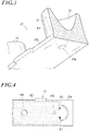
FIG. 3 is a cross-sectional view of a main part illustrating an example in which a sphere is located inside a first protrusion so as to be tangent to the wall surface. -
FIG. 4 is a bottom view illustrating an example of a projected region and a mirror surface region of a first substrate. -
FIG. 5 is an enlarged view of a main part illustrating an example of a projected region and a processed region of a first substrate. -
FIG. 6 is a bottom view illustrating an example in which the mirror surface region is included in a region where a region having a thickness value of 70 to 95% is projected on the first substrate. -
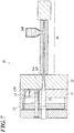
FIG. 7 is a schematic diagram illustrating a mold clamping step. -
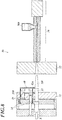
FIG. 8 is a schematic diagram illustrating an ejection step. -
FIG. 9 illustrates examples and comparative examples of test chip substrates. - Hereinafter, embodiments of the present invention will be described with reference to the accompanying drawings.
- A
test chip 10 according to the present embodiment is a chip (micro fluid chip) used for test, analysis, and so on of a biological material based on an antigen-antibody reaction. As illustrated inFIGS. 1 and 2 , thetest chip 10 includes atest chip substrate 12, afirst protrusion 13, and asecond protrusion 14. - The
test chip substrate 12 is made of a resin. The requirements for the resin are high formability (transformability and releasability), high transparency, and low self-fluorescence with respect to the ultraviolet ray and visible ray. Thetest chip substrate 12 has aflow channel 11 through which liquid or the like injected by a non-illustrated liquid feeder flows. - As illustrated in
FIG. 2 , thetest chip substrate 12 includes a first substrate (base) 12a as a thin plate-shaped member, a flow channel seal (not illustrated), and asecond substrate 12b (optical component such as a prism). Theflow channel 11 is formed in a region defined by thefirst substrate 12a and thesecond substrate 12b attached together with a flow channel seal. Thefirst substrate 12a and thesecond substrate 12b of thetest chip substrate 12 are manufactured by a method such as injection molding, press molding, and machine processing. At least one of thefirst substrate 12a and thesecond substrate 12b may be microfabricated. - The
first substrate 12a has a gate GA. The gate GA serves as an inlet when injecting a resin material into the mold. The gate GA has a bridging function for filling the cavity with the resin material injected through a sprue. - The
test chip substrate 12 is formed by joining thefirst substrate 12a and thesecond substrate 12b. When thefirst substrate 12a and thesecond substrate 12b are joined, theflow channel 11 is formed therebetween. The substrates may be joined by a welding method that joins resin-made substrates by heating them using a heat plate, hot air, a heating roller, ultrasonic wave, vibration, laser, double-sided seal, or the like, a bonding method that joins resin-made substrates using adhesive or solution, a method that joins resin-made substrates utilizing their own adhesiveness, or a method that joins substrates by applying surface treatment such as plasma treatment to resin-made substrates. In this manner, thetest chip 10 having theflow channel 11 therein is manufactured. - The
flow channel 11 includes areaction channel 15 extending in a predetermined direction (direction along anupper surface 12c of thetest chip substrate 12 inFIG. 2 ) inside thetest chip substrate 12, acommunication channel 16 for communication between thereaction channel 15 and thefirst protrusion 13, and acommunication channel 17 for communication between thereaction channel 15 and thesecond protrusion 14. - The following describes how the
flow channel 11 is formed. A groove for a flow channel (a part corresponding to thereaction channel 15 inFIG. 2 ) is formed in thesecond substrate 12b. Then, thefirst substrate 12a serving as a cover is joined to thesecond substrate 12b having the flow channel groove, in a manner such that the flow channel groove faces inward. In this way, theflow channel 11 is formed. Alternatively, the flow channel i i may be formed by joining thefirst substrate 12a and thesecond substrate 12b, in a manner such that a double-sided seal having theflow channel 11 is interposed therebetween. - The plate thickness of the
second substrate 12b having the flow channel groove is preferably 0.2 mm to 5 mm, more preferably 0.5 mm to 2 mm. The plate thickness of thefirst substrate 12a serving as a lid (cover) for the flow channel groove is preferably 0.2 mm to 5 mm, more preferably 0.5 mm to 2 mm, taking into account the formability. - The
test chip substrate 12 is made of a low-cost, disposable resin, specifically a thermoplastic resin. Preferred examples of thermoplastic resins are polycarbonate, polymethylmethacrylate, polystyrene, polyacrylonitrile, polyvinyl chloride, polyethylene terephthalate, nylon 6, nylon 66, polyvinyl acetate, polyvinylidene chloride, polypropylene, polypropylene, polyisoprene, polyethylene, polydimethylsiloxane, and cyclic polyolefin. Particularly preferred examples are polymethylmethacrylate and cyclic polyolefin. - The
first protrusion 13 is integrally formed on the upper surface of the test chip substrate 12 (first substrate 12a). Thefirst protrusion 13 has aninner diameter portion 21, and serves as a reagent mixer and a reagent reactor for mixing and reacting a reagent in theinner diameter portion 21. Techniques for mixing and reacting a reagent are well known in the art, and will not be described herein. Theinner diameter portion 21 communicates with thecommunication channel 16 of theflow channel 11. - The
second protrusion 14 is integrally formed on the upper surface of thetest chip substrate 12, but in a region different from the region where thefirst protrusion 13 is formed. Thesecond protrusion 14 has aninner diameter portion 22. Theinner diameter portion 22 communicates with thecommunication channel 17 of theflow channel 11. - The
first protrusion 13 and thesecond protrusion 14 respectively haveholes first substrate 12a. Theholes first protrusion 13 and second protrusion 14) are connected through another component (second substrate 12b) to form theflow channel 11. - Each of the
first protrusion 13 and thesecond protrusion 14 is formed to have a thickness greater than a plate thickness of thefirst substrate 12a. In the present embodiment, the thickness of the thickest portion of the protrusions is two or more times greater than the plate thickness of thefirst substrate 12a. - As illustrated in
FIG. 3 , the thickest portion of the protrusions is the center of a sphere BA that is the largest imaginary sphere located inside the injection molded article (inside thefirst protrusion 13 in the present embodiment) and tangent to the wall surface thereof. The thickest portion of the protrusion can be calculated with, for example, the maximum ball algorithm used in 3D shape analysis software. - As illustrated in
FIG. 4 , when a thickness value of the thickest portion of the protrusions (in the present embodiment, the thickest portion of the first protrusion 13) is defined as 100%, a processed region processed to have a surface roughness greater (by several nanometers to several tens of nanometers in Ra) than the surface roughness of a mirror surface region E2 including a region between theholes first substrate 12a is formed in a projected region E1 (that is, a region where a perpendicular line is drawn from a region having a thickness value of 95 to 100% to thefirst substrate 12a) where a region having a thickness value of 95 to 100% is projected on thefirst substrate 12a. In the present embodiment, the surface roughness of the processed region is 1 to 2 µm in Ra (arithmetic average roughness). - The injection molded article of the present invention is the
test chip 10 excluding thesecond substrate 12b that is an optical component. - As illustrated in
FIG. 5 , when the area of a smallest circle C1 containing the projected region E1 is defined as 100%, the injection molded article of the present invention is obtained from a mold roughened (for example, sandblasted) to make the surface roughness greater than the surface roughness of the mirror surface region E2, in an area of a circle (= processed region E3) that is within the smallest circle C1 and is 50 to 100% of the area of the smallest circle C1. In the present embodiment, for purposes of explanation, the projected region E1 is circular, and the projected region E1 and the smallest circle C1 exactly coincide. However, the present invention is not limited thereto. That is, the projected region E1 is not always circular, and hence the projected region E1 and the smallest circle C1 do not always coincide. Also, the processed region E3 is not always circular, and may have any shape as long as its area is in the range of 50 to 100% of the area of the smallest circle C1. - The injection molded article of the present invention is obtained by injection molding a molten resin into a mold that is processed such that the mirror surface region E2 and the projected region E1 are located close to each other. Specifically, as illustrated in
FIG. 6 , the mirror surface region E2 is included in a region E4 (a region adjacent to the projected region E1) where a region having a thickness value of 70 to 95% is projected on thefirst substrate 12a. That is, the mirror surface E2 is located close to the projected region E1 where sink marks are likely to be formed. Although it is necessary to prevent formation of sink marks, roughening cannot be applied to the mirror surface region E2 because flatness and specularity are required there. Accordingly, in the present embodiment, roughening is applied to the region close to the mirror surface region E2. That is, according to the present invention, even when the region (projected region E1) where sink marks are likely to be formed and the region (mirror surface region E2) requiring flatness and specularity are close to each other, formation of sink marks on the visible surface of thefirst substrate 12a is prevented. - The
test chip 10 is produced through a predetermined process by using an injection molding machine (injection mold 30). Hereafter, the injection molding process using theinjection mold 30 will be described with reference toFIGS. 7 and8 .FIG. 7 is a schematic diagram illustrating a so-called "mold clamping step" for forming a cavity by clamping two molds (movable mold 31 and fixed mold 32).FIG. 8 is a schematic diagram illustrating a so-called "ejection step" for removing an injection moldedarticle 40 from theinjection mold 30. - As illustrated in
FIG. 7 , theinjection mold 30 includes themovable mold 31 with a recess (cavity) 310 in the shape of the injection moldedarticle 40, the fixedmold 32 against which themovable mold 31 is pressed so as to close therecess 310, anejector pin 33 that pushes the injection moldedarticle 40 outward (in the direction of the arrow X inFIG. 8 ), anejector member 34, core pins 35 each defining the internal shape of a protrusion, and acylinder unit 36 that supplies a resin material (not illustrated) as the material of the injection moldedarticle 40 to the cavity. - The injection molding process includes a mold clamping step, an injection step, a pressure holding step, a cooling step, a mold opening step, and an ejection step. Injection molding is performed in this order. As illustrated in
FIG. 7 , in the mold clamping step, themovable mold 31 and the fixedmold 32 are clamped together to close therecess 310 formed in themovable mold 31, thereby forming a cavity. Then, a resin material (molten resin) is injected from a resinmaterial supply furnace 360 to fill the cavity therewith (injection step). The resin material flows through a sprue SP (unwanted portion of the injection molded article 40) and the gate GA, and is filled in the cavity. When filled in the cavity of the mold, the resin material is cooled and shrinks in the mold. Since the shrinkage causes a change in the volume, this shrinkage action results in a dimensional change of a molded article, a shape transfer failure, and the like. To prevent these issues, the volume of resin reduced due to the shrinkage is compensated for by applying a holding pressure on the molding machine side (pressure holding step). Then, the resin material is cooled in the mold until its temperature decreases to a level at which it can be extracted from the mold (cooling step). - When the resin material is sufficiently cooled after a lapse of a predetermined time, the
movable mold 31 is separated from the fixed mold 32 (mold opening step) as illustrated inFIG. 8 . In this step, the molded article comes with themovable mold 31. Then, by moving theejector pin 33 and theejector member 34 outward, the injection moldedarticle 40 is demolded (ejection step). Thesecond substrate 12b is joined to the injection moldedarticle 40 to obtain atest chip 10. - In the present embodiment, since the predetermined region (the region corresponding to the processed region of the
first substrate 12a) of the surface of the fixedmold 32 is roughened (sandblasted), resin is not easily separated from the fixedmold 32 during cooling and shrinkage. This prevents formation of sink marks on the visible surface of the injection molded article 40 (first substrate 12a). - In the following, Examples 1 to 3 and Comparative Examples 1 to 3 of the test chip substrate 12 (
first substrate 12a) according to the present invention will be described with reference toFIG. 9 . - A
test chip substrate 12 of Comparative Example 1 is configured such that the plate thickness of afirst substrate 12a (base plate thickness) is 1.3 mm, and the thickness value of the thickest portion of thefirst substrate 12a is 4.2 mm. The area of a smallest circle C1 containing a projected region E1 is 1.4n mm2; the area of a processed region E3 is 1π mm2; and the ratio (percentage) of the area of a processed region E3 to the area of the smallest circle C1 is 71%. The surface roughness of the processed region E3 is 0.5 µm in Ra. - A
test chip substrate 12 of Comparative Example 2 is configured such that the plate thickness of afirst substrate 12a (base plate thickness) is 1.3 mm, and the thickness value of the thickest portion of thefirst substrate 12a is 4.2 mm. The area of a smallest circle C1 containing a projected region E1 is 1.4π mm2; the area of a processed region E3 is 1π mm2; and the ratio (percentage) of the area of a processed region E3 to the area of the smallest circle C1 is 71%. The surface roughness of the processed region E3 is 3 µm in Ra. - A
test chip substrate 12 of Comparative Example 3 is configured such that the plate thickness of afirst substrate 12a (base plate thickness) is 1.3 mm, and the thickness value of the thickest portion of thefirst substrate 12a is 4.2 mm. The area of a smallest circle C1 containing a projected region E1 is 1.4π mm2; the area of a processed region E3 is 0.5π mm2; and the ratio (percentage) of the area of a processed region E3 to the area of the smallest circle C1 is 36%. The surface roughness of the processed region E3 is 1 µm in Ra. - A
test chip substrate 12 of Example 1 is configured such that the plate thickness of afirst substrate 12a (base plate thickness) is 1.3 mm, and the thickness value of the thickest portion of thefirst substrate 12a is 4.2 mm. The area of a smallest circle C1 containing a projected region E1 is 1.4π mm2; the area of a processed region E3 is 1π mm2; and the ratio (percentage) of the area of a processed region E3 to the area of the smallest circle C1 is 71 %. The surface roughness of the processed region E3 is 1 µm in Ra. - A
test chip substrate 12 of Example 2 is configured such that the plate thickness of afirst substrate 12a (base plate thickness) is 1.3 mm, and the thickness value of the thickest portion of thefirst substrate 12a is 4.2 mm. The area of a smallest circle C1 containing a projected region E1 is 1.4π mm2; the area of a processed region E3 is 1π mm2; and the ratio (percentage) of the area of a processed region E3 to the area of the sm allest circle C1 is 71%. The surface roughness of the processed region E3 is 2 µm in Ra. - A
test chip substrate 12 of Example 3 is configured such that the plate thickness of afirst substrate 12a (base plate thickness) is 1.3 mm, and the thickness value of the thickest portion of thefirst substrate 12a is 4.2 mm. The area of a smallest circle C1 containing a projected region E1 is 1.4π mm2; the area of a processed region E3 is 0.7π mm2; and the ratio (percentage) of the area of a processed region E3 to the area of the smallest circle C1 is 50%. The surface roughness of the processed region E3 is 1 µm in Ra. - In the case of the
test chip substrate 12 of Comparative Example 1 configured such that the surface roughness of the processed region E3 is 0.5 µm in Ra, since the roughness was too low, the resin did not properly stick to the mold. Accordingly, satisfactory results were not obtained. - In the case of the
test chip substrate 12 of Comparative Example 2 configured such that the surface roughness of the processed region E3 is 3 µm in Ra, since the roughness was too high, the resin remained in the mold. Accordingly, satisfactory results were not obtained. - In the case of the
test chip substrate 12 of Comparative Example 3 configured such that the ratio (percentage) of the area of the processed region E3 to the area of the smallest circle C1 is 36%, since the area was too small, the resin did not properly stick to the mold. Accordingly, satisfactory results were not obtained. - Meanwhile, in the case of the
test chip substrates 12 of Examples 1 to 3, satisfactory results were obtained. - It was found from the above that when the
test chip substrate 12 is configured such that the surface roughness of the processed region E3 is 1 to 2 µm in Ra, satisfactory results are obtained. It was also found that when thetest chip substrate 12 is configured such that the ratio (percentage) of the area of the processed region E3 to the area of the smallest circle C1 is 50 to 100%, satisfactory results are obtained. - With any of the configurations of Examples 1 to 3, it is possible to prevent formation of sink marks on the visible surface of the
first substrate 12a. - Meanwhile, a region where the surface accuracy of the mold is not achieved is formed in a region where the region of the thickest portion is projected on the invisible surface (for example, the side wall of the protrusion) defining the surface other than the visible surface. The region where the surface accuracy of the mold is not achieved is a region where the shape of the mold is not accurately transferred, and is a region where a so-called sink mark is formed. That is, in the present embodiment, formation of sink marks on the visible surface of the
first substrate 12a is prevented by guiding sink marks to the invisible surface. - As described above, the injection molded article according to the present embodiment includes: a base (
first substrate 12a) as a thin plate-shaped member that is connected to the gate GA of a mold (injection mold 30); and a plurality of protrusions (first protrusion 13 and second protrusion 14) each integrally molded on the base and having a thickness greater than a plate thickness of the base. The plurality of protrusions haveholes holes holes - Accordingly, according to the injection molded article of the present embodiment, the region of the product visible surface in which sink marks are likely to be formed is processed such that resin is not easily separated, so that formation of sink marks on the product visible surface is prevented. Accordingly, the surface properties of the product visible surface are sufficiently secured. Therefore, it is possible to prevent leakage of liquid, and achieve the required accuracy in height of the flow channel.
- According to the injection molded article of the present embodiment, the thickness of the thickest portion is two or more times greater than the plate thickness of the base.
- Accordingly, according to the injection molded article of the present embodiment, even when the molded artic has a large thickness, formation of sink marks on the visible surface is prevented. Therefore, it is possible to prevent leakage of liquid, and achieve the required accuracy in height of the flow channel.
- According to the injection molded article of the present embodiment, the surface roughness of the processed region E3 is 1 - 2 µm in Ra.
- Accordingly, according to the injection molded article of the present embodiment, the resin on the product visible surface side adheres sufficiently well, so that formation of sink marks on the product visible surface is more reliably prevented.
- According to the injection molded article of the present embodiment, when the area of the smallest circle C1 containing the projected region E1 is defined as 100%, the injection molded article is obtained from a mold roughened to make the surface roughness greater than the surface roughness of the mirror surface region E2, in an area that is within the smallest circle C1 and that is 50 to 100% of the area of the smallest circle C1.
- Accordingly, according to the injection molded article of the present embodiment, the resin on the product visible surface side adheres sufficiently well, so that formation of sink marks on the product visible surface is more reliably prevented.
- According to the injection molded article of the present embodiment, a region where a surface accuracy of the mold is not achieved is formed in a region where a region of the thickest portion is projected on an invisible surface defining a surface other than the base.
- Accordingly, according to the injection molded article of the present embodiment, sink marks are guided to the invisible surface, so that formation of sink marks on the product visible surface is prevented.
- According to the injection molded article of the present embodiment, the mirror surface region E2 is included in a region where a region having a thickness value of 70 to 95% is projected on the base.
- Accordingly, according to the injection molded article of the present embodiment, even when the region (projected region E1) where sink marks are likely to be formed and the region (mirror surface region E2) requiring flatness and specularity are close to each other, formation of sink marks on the visible surface is prevented. Therefore, it is possible to prevent leakage of liquid, and achieve the required accuracy in height of the flow channel.
- Although the present invention has been described in conjunction with the specific embodiment, the present invention is not limited to the above embodiment, and changes and modifications may be made without departing from the scope of the present invention.
- For example, in the above embodiment, the thickness of the thickest portion of the protrusions is two or more times greater than the plate thickness of the
first substrate 12a. However, the present invention is not limited thereto. That is, the thickness of the thickest portion of the protrusions only needs to be greater than the plate thickness of thefirst substrate 12a. The thickness of the thickest portion of the protrusions may be less than twice the thickness of thefirst substrate 12a. - In the above embodiment, surface roughening is performed by sandblasting. However, the present invention is not limited thereto. For example, surface roughening is performed by rubbing with sand paper or etching, in place of sandblasting. Alternatively, fine indentations may be formed on the surface by using a processing machine capable of high precision processing so as to have a desired surface roughness (Ra).
- Other changes and modifications may also be made to the configuration and operation of the devices included in the test chip without departing from the scope of the present invention.
- The present invention is applicable to injection molded articles.
-
- 10
- test chip
- 11
- flow path
- 12
- test chip substrate
- 12a
- first substrate (base)
- 12b
- second substrate
- 13
- first protrusion (protrusion)
- 14
- second protrusion (protrusion)
- 13a, 14a
- hole
- 15
- reaction channel
- 16, 17
- communication channel
- 21, 22
- inner diameter portion
- 30
- injection mold
- 31
- movable mold
- 310
- recess
- 32
- fixed mold
- 33
- ejector pin
- 34
- ejector member
- 35
- core pin
- 36
- cylinder unit
- 360
- resin material supply furnace
- 40
- injection molded article
- GA
- gate
- BA
- sphere
- E1
- projected region
- E2
- mirror surface region
- E3
- processed region
- C1
- smallest circle
Claims (6)
- An injection molded article that is obtained by injection molding a molten resin into a mold, the injection molded article comprising:a base as a thin plate-shaped member that is connected to a gate of the mold; anda plurality of protrusions each integrally molded on the base and having a thickness greater than a plate thickness of the base;wherein the plurality of protrusions have holes each extending through the base, and the holes in the respective protrusions are connected through another component to form a flow channel;wherein when a thickness value of a thickest portion of the protrusions is defined as 100%, a processed region processed to have a surface roughness greater than a surface roughness of a mirror surface region including a region between the holes on the base is formed in a projected region where a region having a thickness value of 95 to 100% is projected on the base; andwherein the injection molded article is obtained from the mold processed such that the mirror surface region and the projected region are located close to each other.
- The injection molded article according to claim 1, wherein the thickness of the thickest portion is two or more times greater than the plate thickness of the base.
- The injection molded article according to claim 1 or 2, wherein the surface roughness of the processed region is 1 to 2 µm in Ra.
- The injection molded article according to any one of claims 1 to 3, wherein when an area of a smallest circle containing the projected region is defined as 100%, the injection molded article is obtained from the mold roughened to make a surface roughness greater than the surface roughness of the mirror surface region, in an area that is within the smallest circle and is 50 to 100% of an area of the smallest circle.
- The injection molded article according to any one of claims 1 to 4, wherein a region where a surface accuracy of the mold is not achieved is formed in a region where a region of the thickest portion is projected on an invisible surface defining a surface other than the base.
- The injection molded article according to any one of claims 1 to 5, wherein the mirror surface region is included in a region where a region having a thickness value of 70 to 95% is projected on the base.
Applications Claiming Priority (2)
| Application Number | Priority Date | Filing Date | Title |
|---|---|---|---|
| JP2017240129 | 2017-12-15 | ||
| PCT/JP2018/036216 WO2019116680A1 (en) | 2017-12-15 | 2018-09-28 | Injection molded article |
Publications (3)
| Publication Number | Publication Date |
|---|---|
| EP3702123A1 true EP3702123A1 (en) | 2020-09-02 |
| EP3702123A4 EP3702123A4 (en) | 2020-12-09 |
| EP3702123B1 EP3702123B1 (en) | 2024-09-11 |
Family
ID=66819603
Family Applications (1)
| Application Number | Title | Priority Date | Filing Date |
|---|---|---|---|
| EP18888242.7A Active EP3702123B1 (en) | 2017-12-15 | 2018-09-28 | Injection molded article |
Country Status (5)
| Country | Link |
|---|---|
| US (1) | US11565450B2 (en) |
| EP (1) | EP3702123B1 (en) |
| JP (1) | JP7104719B2 (en) |
| ES (1) | ES2989354T3 (en) |
| WO (1) | WO2019116680A1 (en) |
Families Citing this family (6)
| Publication number | Priority date | Publication date | Assignee | Title |
|---|---|---|---|---|
| CN112522913B (en) * | 2020-11-30 | 2024-06-21 | 无锡小天鹅电器有限公司 | Appearance part, household appliance and mold |
| WO2022110497A1 (en) * | 2020-11-30 | 2022-06-02 | 无锡小天鹅电器有限公司 | Appearance part, household appliance and mold |
| CN112522914B (en) * | 2020-11-30 | 2024-06-25 | 无锡小天鹅电器有限公司 | Appearance part, household appliance and mold |
| WO2022110498A1 (en) * | 2020-11-30 | 2022-06-02 | 无锡小天鹅电器有限公司 | Appearance part, household appliance and mold |
| JP7605055B2 (en) * | 2021-07-21 | 2024-12-24 | 住友電装株式会社 | Injection moldings and sensor modules |
| CN113619145A (en) * | 2021-08-10 | 2021-11-09 | 广州精诚橡塑制品有限公司 | Forming process of lining-containing shoe |
Family Cites Families (10)
| Publication number | Priority date | Publication date | Assignee | Title |
|---|---|---|---|---|
| JPH06315955A (en) * | 1993-05-10 | 1994-11-15 | Tohoku Munekata Kk | Method and apparatus for manufacturing injection-molded plastic product that does not cause sink mark on visible surface |
| JP2003139065A (en) | 2001-11-02 | 2003-05-14 | Kawamura Inst Of Chem Res | Microfluid device having diaphragm type pump mechanism, pump driving device and fluid transfer method |
| JP2005163585A (en) | 2003-12-01 | 2005-06-23 | Kawamura Inst Of Chem Res | Micro fluid device pump and fluid transfer method |
| JP2005231239A (en) * | 2004-02-20 | 2005-09-02 | Ricoh Co Ltd | Molding method, injection molding apparatus, injection compression molding apparatus, molding die, optical disc master, and optical disc |
| JPWO2010016372A1 (en) | 2008-08-06 | 2012-01-19 | コニカミノルタオプト株式会社 | Microchip |
| JP5282273B2 (en) | 2008-08-08 | 2013-09-04 | コニカミノルタ株式会社 | Microchip and manufacturing method of microchip |
| JP2012098074A (en) | 2010-10-29 | 2012-05-24 | Konica Minolta Opto Inc | Method for producing microchip |
| JP2013176958A (en) * | 2012-01-31 | 2013-09-09 | Technocrats Corp | Molding |
| JP5838863B2 (en) * | 2012-03-05 | 2016-01-06 | コニカミノルタ株式会社 | Injection molded products and inspection chips |
| JP6412435B2 (en) | 2015-02-06 | 2018-10-24 | 信越ポリマー株式会社 | Microchannel chip |
-
2018
- 2018-09-28 ES ES18888242T patent/ES2989354T3/en active Active
- 2018-09-28 JP JP2019558924A patent/JP7104719B2/en active Active
- 2018-09-28 US US16/765,316 patent/US11565450B2/en active Active
- 2018-09-28 EP EP18888242.7A patent/EP3702123B1/en active Active
- 2018-09-28 WO PCT/JP2018/036216 patent/WO2019116680A1/en not_active Ceased
Also Published As
| Publication number | Publication date |
|---|---|
| ES2989354T3 (en) | 2024-11-26 |
| JP7104719B2 (en) | 2022-07-21 |
| EP3702123B1 (en) | 2024-09-11 |
| EP3702123A4 (en) | 2020-12-09 |
| WO2019116680A1 (en) | 2019-06-20 |
| US20200353658A1 (en) | 2020-11-12 |
| JPWO2019116680A1 (en) | 2020-12-03 |
| US11565450B2 (en) | 2023-01-31 |
Similar Documents
| Publication | Publication Date | Title |
|---|---|---|
| EP3702123B1 (en) | Injection molded article | |
| US20100327470A1 (en) | Process and apparatus for producing thick-walled plastic components | |
| JP2008279784A (en) | Plastic molded product | |
| US7615274B2 (en) | Storage magazine for microstructured molded parts and fabrication procedure | |
| JPWO2004103682A1 (en) | MOLDING METHOD, MOLD FOR MOLDING, MOLDED ARTICLE, AND MOLDING MACHINE | |
| AU758228B2 (en) | Insert part stuck cylindrical article, its forming method, and its forming device | |
| US8377362B2 (en) | Method for manufacturing micro-channel, die for molding micro-channel chip, and micro-channel chip | |
| JPWO2010016359A1 (en) | Microchip and manufacturing method of microchip | |
| CN115256819B (en) | Substrate injection mold, microfluidic chip injection mold and bonding method | |
| US10160145B2 (en) | Microfluidic device | |
| US20100237536A1 (en) | Mold for in-mold coating and in-mold coating method | |
| JP4312675B2 (en) | Method and apparatus for producing molded body | |
| JP4108269B2 (en) | Resin molding apparatus and resin molding method | |
| JP5637649B2 (en) | Injection mold, thin plate-shaped molded product | |
| JP5838863B2 (en) | Injection molded products and inspection chips | |
| JP2004155018A (en) | Resin molding method and resin molding machine | |
| CN109421206A (en) | The mold and insert-molded article of insert molding method, insert-molding | |
| KR102133679B1 (en) | Biochip quick delivery molding based on mold base standardized by the biochip size | |
| JP2008290335A (en) | Method for forming fine pattern | |
| Yoon et al. | Enhancement of surface replication by gas assisted microinjection moulding | |
| JP2010195000A (en) | In-mold transfer mold and method for manufacturing in-molded transferred article | |
| CN118456995A (en) | Flexible film, in-mold insert injection structure, equipment with structure and processing method of equipment | |
| Kolew et al. | Multi-component hot embossing of micro-and nanosystems | |
| Kosse et al. | Microthermoforming and Sealing of COP Films to Form Thin Walled Lab-On-A-Chip Cartridges | |
| JP2008062400A (en) | Mold |
Legal Events
| Date | Code | Title | Description |
|---|---|---|---|
| STAA | Information on the status of an ep patent application or granted ep patent |
Free format text: STATUS: THE INTERNATIONAL PUBLICATION HAS BEEN MADE |
|
| PUAI | Public reference made under article 153(3) epc to a published international application that has entered the european phase |
Free format text: ORIGINAL CODE: 0009012 |
|
| STAA | Information on the status of an ep patent application or granted ep patent |
Free format text: STATUS: REQUEST FOR EXAMINATION WAS MADE |
|
| 17P | Request for examination filed |
Effective date: 20200527 |
|
| AK | Designated contracting states |
Kind code of ref document: A1 Designated state(s): AL AT BE BG CH CY CZ DE DK EE ES FI FR GB GR HR HU IE IS IT LI LT LU LV MC MK MT NL NO PL PT RO RS SE SI SK SM TR |
|
| AX | Request for extension of the european patent |
Extension state: BA ME |
|
| A4 | Supplementary search report drawn up and despatched |
Effective date: 20201109 |
|
| RIC1 | Information provided on ipc code assigned before grant |
Ipc: B29C 33/42 20060101AFI20201103BHEP Ipc: B29C 45/26 20060101ALI20201103BHEP Ipc: B29C 45/00 20060101ALI20201103BHEP |
|
| DAV | Request for validation of the european patent (deleted) | ||
| DAX | Request for extension of the european patent (deleted) | ||
| STAA | Information on the status of an ep patent application or granted ep patent |
Free format text: STATUS: EXAMINATION IS IN PROGRESS |
|
| 17Q | First examination report despatched |
Effective date: 20220215 |
|
| RAP1 | Party data changed (applicant data changed or rights of an application transferred) |
Owner name: OTSUKA PHARMACEUTICAL CO., LTD. |
|
| GRAP | Despatch of communication of intention to grant a patent |
Free format text: ORIGINAL CODE: EPIDOSNIGR1 |
|
| STAA | Information on the status of an ep patent application or granted ep patent |
Free format text: STATUS: GRANT OF PATENT IS INTENDED |
|
| INTG | Intention to grant announced |
Effective date: 20240531 |
|
| GRAS | Grant fee paid |
Free format text: ORIGINAL CODE: EPIDOSNIGR3 |
|
| GRAA | (expected) grant |
Free format text: ORIGINAL CODE: 0009210 |
|
| STAA | Information on the status of an ep patent application or granted ep patent |
Free format text: STATUS: THE PATENT HAS BEEN GRANTED |
|
| P01 | Opt-out of the competence of the unified patent court (upc) registered |
Free format text: CASE NUMBER: APP_40305/2024 Effective date: 20240707 |
|
| AK | Designated contracting states |
Kind code of ref document: B1 Designated state(s): AL AT BE BG CH CY CZ DE DK EE ES FI FR GB GR HR HU IE IS IT LI LT LU LV MC MK MT NL NO PL PT RO RS SE SI SK SM TR |
|
| REG | Reference to a national code |
Ref country code: GB Ref legal event code: FG4D |
|
| REG | Reference to a national code |
Ref country code: CH Ref legal event code: EP |
|
| REG | Reference to a national code |
Ref country code: DE Ref legal event code: R096 Ref document number: 602018074385 Country of ref document: DE |
|
| REG | Reference to a national code |
Ref country code: IE Ref legal event code: FG4D |
|
| REG | Reference to a national code |
Ref country code: ES Ref legal event code: FG2A Ref document number: 2989354 Country of ref document: ES Kind code of ref document: T3 Effective date: 20241126 |
|
| REG | Reference to a national code |
Ref country code: LT Ref legal event code: MG9D |
|
| PG25 | Lapsed in a contracting state [announced via postgrant information from national office to epo] |
Ref country code: NO Free format text: LAPSE BECAUSE OF FAILURE TO SUBMIT A TRANSLATION OF THE DESCRIPTION OR TO PAY THE FEE WITHIN THE PRESCRIBED TIME-LIMIT Effective date: 20241211 |
|
| REG | Reference to a national code |
Ref country code: NL Ref legal event code: MP Effective date: 20240911 |
|
| PG25 | Lapsed in a contracting state [announced via postgrant information from national office to epo] |
Ref country code: GR Free format text: LAPSE BECAUSE OF FAILURE TO SUBMIT A TRANSLATION OF THE DESCRIPTION OR TO PAY THE FEE WITHIN THE PRESCRIBED TIME-LIMIT Effective date: 20241212 Ref country code: FI Free format text: LAPSE BECAUSE OF FAILURE TO SUBMIT A TRANSLATION OF THE DESCRIPTION OR TO PAY THE FEE WITHIN THE PRESCRIBED TIME-LIMIT Effective date: 20240911 |
|
| PG25 | Lapsed in a contracting state [announced via postgrant information from national office to epo] |
Ref country code: BG Free format text: LAPSE BECAUSE OF FAILURE TO SUBMIT A TRANSLATION OF THE DESCRIPTION OR TO PAY THE FEE WITHIN THE PRESCRIBED TIME-LIMIT Effective date: 20240911 |
|
| PG25 | Lapsed in a contracting state [announced via postgrant information from national office to epo] |
Ref country code: LV Free format text: LAPSE BECAUSE OF FAILURE TO SUBMIT A TRANSLATION OF THE DESCRIPTION OR TO PAY THE FEE WITHIN THE PRESCRIBED TIME-LIMIT Effective date: 20240911 |
|
| PG25 | Lapsed in a contracting state [announced via postgrant information from national office to epo] |
Ref country code: HR Free format text: LAPSE BECAUSE OF FAILURE TO SUBMIT A TRANSLATION OF THE DESCRIPTION OR TO PAY THE FEE WITHIN THE PRESCRIBED TIME-LIMIT Effective date: 20240911 |
|
| PG25 | Lapsed in a contracting state [announced via postgrant information from national office to epo] |
Ref country code: RS Free format text: LAPSE BECAUSE OF FAILURE TO SUBMIT A TRANSLATION OF THE DESCRIPTION OR TO PAY THE FEE WITHIN THE PRESCRIBED TIME-LIMIT Effective date: 20241211 |
|
| PG25 | Lapsed in a contracting state [announced via postgrant information from national office to epo] |
Ref country code: RS Free format text: LAPSE BECAUSE OF FAILURE TO SUBMIT A TRANSLATION OF THE DESCRIPTION OR TO PAY THE FEE WITHIN THE PRESCRIBED TIME-LIMIT Effective date: 20241211 Ref country code: NO Free format text: LAPSE BECAUSE OF FAILURE TO SUBMIT A TRANSLATION OF THE DESCRIPTION OR TO PAY THE FEE WITHIN THE PRESCRIBED TIME-LIMIT Effective date: 20241211 Ref country code: LV Free format text: LAPSE BECAUSE OF FAILURE TO SUBMIT A TRANSLATION OF THE DESCRIPTION OR TO PAY THE FEE WITHIN THE PRESCRIBED TIME-LIMIT Effective date: 20240911 Ref country code: HR Free format text: LAPSE BECAUSE OF FAILURE TO SUBMIT A TRANSLATION OF THE DESCRIPTION OR TO PAY THE FEE WITHIN THE PRESCRIBED TIME-LIMIT Effective date: 20240911 Ref country code: GR Free format text: LAPSE BECAUSE OF FAILURE TO SUBMIT A TRANSLATION OF THE DESCRIPTION OR TO PAY THE FEE WITHIN THE PRESCRIBED TIME-LIMIT Effective date: 20241212 Ref country code: FI Free format text: LAPSE BECAUSE OF FAILURE TO SUBMIT A TRANSLATION OF THE DESCRIPTION OR TO PAY THE FEE WITHIN THE PRESCRIBED TIME-LIMIT Effective date: 20240911 Ref country code: BG Free format text: LAPSE BECAUSE OF FAILURE TO SUBMIT A TRANSLATION OF THE DESCRIPTION OR TO PAY THE FEE WITHIN THE PRESCRIBED TIME-LIMIT Effective date: 20240911 |
|
| REG | Reference to a national code |
Ref country code: AT Ref legal event code: MK05 Ref document number: 1722321 Country of ref document: AT Kind code of ref document: T Effective date: 20240911 |
|
| PG25 | Lapsed in a contracting state [announced via postgrant information from national office to epo] |
Ref country code: NL Free format text: LAPSE BECAUSE OF FAILURE TO SUBMIT A TRANSLATION OF THE DESCRIPTION OR TO PAY THE FEE WITHIN THE PRESCRIBED TIME-LIMIT Effective date: 20240911 |
|
| PG25 | Lapsed in a contracting state [announced via postgrant information from national office to epo] |
Ref country code: IS Free format text: LAPSE BECAUSE OF FAILURE TO SUBMIT A TRANSLATION OF THE DESCRIPTION OR TO PAY THE FEE WITHIN THE PRESCRIBED TIME-LIMIT Effective date: 20250111 Ref country code: PT Free format text: LAPSE BECAUSE OF FAILURE TO SUBMIT A TRANSLATION OF THE DESCRIPTION OR TO PAY THE FEE WITHIN THE PRESCRIBED TIME-LIMIT Effective date: 20250113 |
|
| PG25 | Lapsed in a contracting state [announced via postgrant information from national office to epo] |
Ref country code: SM Free format text: LAPSE BECAUSE OF FAILURE TO SUBMIT A TRANSLATION OF THE DESCRIPTION OR TO PAY THE FEE WITHIN THE PRESCRIBED TIME-LIMIT Effective date: 20240911 Ref country code: RO Free format text: LAPSE BECAUSE OF FAILURE TO SUBMIT A TRANSLATION OF THE DESCRIPTION OR TO PAY THE FEE WITHIN THE PRESCRIBED TIME-LIMIT Effective date: 20240911 |
|
| PG25 | Lapsed in a contracting state [announced via postgrant information from national office to epo] |
Ref country code: EE Free format text: LAPSE BECAUSE OF FAILURE TO SUBMIT A TRANSLATION OF THE DESCRIPTION OR TO PAY THE FEE WITHIN THE PRESCRIBED TIME-LIMIT Effective date: 20240911 Ref country code: AT Free format text: LAPSE BECAUSE OF FAILURE TO SUBMIT A TRANSLATION OF THE DESCRIPTION OR TO PAY THE FEE WITHIN THE PRESCRIBED TIME-LIMIT Effective date: 20240911 |
|
| PG25 | Lapsed in a contracting state [announced via postgrant information from national office to epo] |
Ref country code: PL Free format text: LAPSE BECAUSE OF FAILURE TO SUBMIT A TRANSLATION OF THE DESCRIPTION OR TO PAY THE FEE WITHIN THE PRESCRIBED TIME-LIMIT Effective date: 20240911 Ref country code: CZ Free format text: LAPSE BECAUSE OF FAILURE TO SUBMIT A TRANSLATION OF THE DESCRIPTION OR TO PAY THE FEE WITHIN THE PRESCRIBED TIME-LIMIT Effective date: 20240911 |
|
| PG25 | Lapsed in a contracting state [announced via postgrant information from national office to epo] |
Ref country code: SK Free format text: LAPSE BECAUSE OF FAILURE TO SUBMIT A TRANSLATION OF THE DESCRIPTION OR TO PAY THE FEE WITHIN THE PRESCRIBED TIME-LIMIT Effective date: 20240911 |
|
| REG | Reference to a national code |
Ref country code: CH Ref legal event code: PL |
|
| PG25 | Lapsed in a contracting state [announced via postgrant information from national office to epo] |
Ref country code: LU Free format text: LAPSE BECAUSE OF NON-PAYMENT OF DUE FEES Effective date: 20240928 |
|
| REG | Reference to a national code |
Ref country code: DE Ref legal event code: R097 Ref document number: 602018074385 Country of ref document: DE |
|
| PG25 | Lapsed in a contracting state [announced via postgrant information from national office to epo] |
Ref country code: MC Free format text: LAPSE BECAUSE OF FAILURE TO SUBMIT A TRANSLATION OF THE DESCRIPTION OR TO PAY THE FEE WITHIN THE PRESCRIBED TIME-LIMIT Effective date: 20240911 |
|
| PG25 | Lapsed in a contracting state [announced via postgrant information from national office to epo] |
Ref country code: DK Free format text: LAPSE BECAUSE OF FAILURE TO SUBMIT A TRANSLATION OF THE DESCRIPTION OR TO PAY THE FEE WITHIN THE PRESCRIBED TIME-LIMIT Effective date: 20240911 |
|
| REG | Reference to a national code |
Ref country code: BE Ref legal event code: MM Effective date: 20240930 |
|
| PG25 | Lapsed in a contracting state [announced via postgrant information from national office to epo] |
Ref country code: BE Free format text: LAPSE BECAUSE OF NON-PAYMENT OF DUE FEES Effective date: 20240930 |
|
| PLBE | No opposition filed within time limit |
Free format text: ORIGINAL CODE: 0009261 |
|
| STAA | Information on the status of an ep patent application or granted ep patent |
Free format text: STATUS: NO OPPOSITION FILED WITHIN TIME LIMIT |
|
| PG25 | Lapsed in a contracting state [announced via postgrant information from national office to epo] |
Ref country code: CH Free format text: LAPSE BECAUSE OF NON-PAYMENT OF DUE FEES Effective date: 20240930 |
|
| PG25 | Lapsed in a contracting state [announced via postgrant information from national office to epo] |
Ref country code: IE Free format text: LAPSE BECAUSE OF NON-PAYMENT OF DUE FEES Effective date: 20240928 |
|
| 26N | No opposition filed |
Effective date: 20250612 |
|
| PG25 | Lapsed in a contracting state [announced via postgrant information from national office to epo] |
Ref country code: SE Free format text: LAPSE BECAUSE OF FAILURE TO SUBMIT A TRANSLATION OF THE DESCRIPTION OR TO PAY THE FEE WITHIN THE PRESCRIBED TIME-LIMIT Effective date: 20240911 |
|
| PGFP | Annual fee paid to national office [announced via postgrant information from national office to epo] |
Ref country code: DE Payment date: 20250820 Year of fee payment: 8 |
|
| PGFP | Annual fee paid to national office [announced via postgrant information from national office to epo] |
Ref country code: IT Payment date: 20250820 Year of fee payment: 8 |
|
| PGFP | Annual fee paid to national office [announced via postgrant information from national office to epo] |
Ref country code: GB Payment date: 20250822 Year of fee payment: 8 |
|
| PGFP | Annual fee paid to national office [announced via postgrant information from national office to epo] |
Ref country code: FR Payment date: 20250821 Year of fee payment: 8 |
|
| PG25 | Lapsed in a contracting state [announced via postgrant information from national office to epo] |
Ref country code: CY Free format text: LAPSE BECAUSE OF FAILURE TO SUBMIT A TRANSLATION OF THE DESCRIPTION OR TO PAY THE FEE WITHIN THE PRESCRIBED TIME-LIMIT; INVALID AB INITIO Effective date: 20180928 |
|
| PGFP | Annual fee paid to national office [announced via postgrant information from national office to epo] |
Ref country code: ES Payment date: 20251001 Year of fee payment: 8 |
|
| PG25 | Lapsed in a contracting state [announced via postgrant information from national office to epo] |
Ref country code: HU Free format text: LAPSE BECAUSE OF FAILURE TO SUBMIT A TRANSLATION OF THE DESCRIPTION OR TO PAY THE FEE WITHIN THE PRESCRIBED TIME-LIMIT; INVALID AB INITIO Effective date: 20180928 |