EP3700191A1 - Imaging device, exposure control method, program, and imaging element - Google Patents
Imaging device, exposure control method, program, and imaging element Download PDFInfo
- Publication number
- EP3700191A1 EP3700191A1 EP18869368.3A EP18869368A EP3700191A1 EP 3700191 A1 EP3700191 A1 EP 3700191A1 EP 18869368 A EP18869368 A EP 18869368A EP 3700191 A1 EP3700191 A1 EP 3700191A1
- Authority
- EP
- European Patent Office
- Prior art keywords
- pixel
- imaging
- directive
- pixel output
- light
- Prior art date
- Legal status (The legal status is an assumption and is not a legal conclusion. Google has not performed a legal analysis and makes no representation as to the accuracy of the status listed.)
- Granted
Links
- 238000003384 imaging method Methods 0.000 title claims abstract description 559
- 238000000034 method Methods 0.000 title claims abstract description 87
- 238000001514 detection method Methods 0.000 claims abstract description 265
- 230000008569 process Effects 0.000 claims description 54
- 230000035945 sensitivity Effects 0.000 claims description 36
- 230000003287 optical effect Effects 0.000 claims description 21
- 238000000605 extraction Methods 0.000 claims description 7
- 238000003780 insertion Methods 0.000 claims description 7
- 230000037431 insertion Effects 0.000 claims description 7
- 230000007935 neutral effect Effects 0.000 claims description 6
- 230000000875 corresponding effect Effects 0.000 description 50
- 239000011159 matrix material Substances 0.000 description 42
- 238000012545 processing Methods 0.000 description 42
- 230000014509 gene expression Effects 0.000 description 29
- 230000001276 controlling effect Effects 0.000 description 22
- 230000008859 change Effects 0.000 description 20
- 238000012546 transfer Methods 0.000 description 18
- 230000007423 decrease Effects 0.000 description 16
- 238000004891 communication Methods 0.000 description 14
- 230000006870 function Effects 0.000 description 11
- 230000004044 response Effects 0.000 description 11
- 238000003860 storage Methods 0.000 description 11
- 230000003321 amplification Effects 0.000 description 10
- 238000004364 calculation method Methods 0.000 description 10
- 238000006243 chemical reaction Methods 0.000 description 10
- 230000004048 modification Effects 0.000 description 10
- 238000012986 modification Methods 0.000 description 10
- 238000003199 nucleic acid amplification method Methods 0.000 description 10
- 238000005516 engineering process Methods 0.000 description 8
- 230000009467 reduction Effects 0.000 description 7
- 238000010586 diagram Methods 0.000 description 6
- 238000009826 distribution Methods 0.000 description 6
- 229910052774 Proactinium Inorganic materials 0.000 description 5
- 230000000694 effects Effects 0.000 description 5
- 229910052745 lead Inorganic materials 0.000 description 5
- NRNCYVBFPDDJNE-UHFFFAOYSA-N pemoline Chemical compound O1C(N)=NC(=O)C1C1=CC=CC=C1 NRNCYVBFPDDJNE-UHFFFAOYSA-N 0.000 description 5
- 238000013461 design Methods 0.000 description 4
- 230000007246 mechanism Effects 0.000 description 4
- 229920006395 saturated elastomer Polymers 0.000 description 4
- 230000002776 aggregation Effects 0.000 description 3
- 238000004220 aggregation Methods 0.000 description 3
- 230000005540 biological transmission Effects 0.000 description 3
- 238000004519 manufacturing process Methods 0.000 description 3
- 239000004065 semiconductor Substances 0.000 description 3
- 101100010712 Caenorhabditis elegans dyn-1 gene Proteins 0.000 description 2
- 230000002238 attenuated effect Effects 0.000 description 2
- 230000006835 compression Effects 0.000 description 2
- 238000007906 compression Methods 0.000 description 2
- 239000010949 copper Substances 0.000 description 2
- 238000012937 correction Methods 0.000 description 2
- 230000002596 correlated effect Effects 0.000 description 2
- 238000009792 diffusion process Methods 0.000 description 2
- 239000006185 dispersion Substances 0.000 description 2
- 238000007667 floating Methods 0.000 description 2
- 229910052751 metal Inorganic materials 0.000 description 2
- 239000002184 metal Substances 0.000 description 2
- 238000005096 rolling process Methods 0.000 description 2
- 238000005070 sampling Methods 0.000 description 2
- 239000007787 solid Substances 0.000 description 2
- 230000000007 visual effect Effects 0.000 description 2
- RYGMFSIKBFXOCR-UHFFFAOYSA-N Copper Chemical compound [Cu] RYGMFSIKBFXOCR-UHFFFAOYSA-N 0.000 description 1
- 230000001133 acceleration Effects 0.000 description 1
- 238000009825 accumulation Methods 0.000 description 1
- 239000000956 alloy Substances 0.000 description 1
- 229910045601 alloy Inorganic materials 0.000 description 1
- 230000004075 alteration Effects 0.000 description 1
- 229910052782 aluminium Inorganic materials 0.000 description 1
- XAGFODPZIPBFFR-UHFFFAOYSA-N aluminium Chemical compound [Al] XAGFODPZIPBFFR-UHFFFAOYSA-N 0.000 description 1
- 230000009194 climbing Effects 0.000 description 1
- 230000000295 complement effect Effects 0.000 description 1
- 229910052802 copper Inorganic materials 0.000 description 1
- 238000013135 deep learning Methods 0.000 description 1
- 230000007613 environmental effect Effects 0.000 description 1
- 238000002474 experimental method Methods 0.000 description 1
- 238000005286 illumination Methods 0.000 description 1
- 230000006872 improvement Effects 0.000 description 1
- 238000009434 installation Methods 0.000 description 1
- 238000005259 measurement Methods 0.000 description 1
- 229910044991 metal oxide Inorganic materials 0.000 description 1
- 150000004706 metal oxides Chemical class 0.000 description 1
- 239000000203 mixture Substances 0.000 description 1
- 230000000704 physical effect Effects 0.000 description 1
- 238000000926 separation method Methods 0.000 description 1
- 239000000126 substance Substances 0.000 description 1
- 230000007704 transition Effects 0.000 description 1
- WFKWXMTUELFFGS-UHFFFAOYSA-N tungsten Chemical compound [W] WFKWXMTUELFFGS-UHFFFAOYSA-N 0.000 description 1
- 229910052721 tungsten Inorganic materials 0.000 description 1
- 239000010937 tungsten Substances 0.000 description 1
Images


Classifications
-
- G—PHYSICS
- G03—PHOTOGRAPHY; CINEMATOGRAPHY; ANALOGOUS TECHNIQUES USING WAVES OTHER THAN OPTICAL WAVES; ELECTROGRAPHY; HOLOGRAPHY
- G03B—APPARATUS OR ARRANGEMENTS FOR TAKING PHOTOGRAPHS OR FOR PROJECTING OR VIEWING THEM; APPARATUS OR ARRANGEMENTS EMPLOYING ANALOGOUS TECHNIQUES USING WAVES OTHER THAN OPTICAL WAVES; ACCESSORIES THEREFOR
- G03B7/00—Control of exposure by setting shutters, diaphragms or filters, separately or conjointly
- G03B7/08—Control effected solely on the basis of the response, to the intensity of the light received by the camera, of a built-in light-sensitive device
-
- H—ELECTRICITY
- H04—ELECTRIC COMMUNICATION TECHNIQUE
- H04N—PICTORIAL COMMUNICATION, e.g. TELEVISION
- H04N23/00—Cameras or camera modules comprising electronic image sensors; Control thereof
- H04N23/70—Circuitry for compensating brightness variation in the scene
- H04N23/73—Circuitry for compensating brightness variation in the scene by influencing the exposure time
-
- G—PHYSICS
- G02—OPTICS
- G02B—OPTICAL ELEMENTS, SYSTEMS OR APPARATUS
- G02B5/00—Optical elements other than lenses
- G02B5/20—Filters
-
- G—PHYSICS
- G02—OPTICS
- G02B—OPTICAL ELEMENTS, SYSTEMS OR APPARATUS
- G02B5/00—Optical elements other than lenses
- G02B5/20—Filters
- G02B5/205—Neutral density filters
-
- G—PHYSICS
- G03—PHOTOGRAPHY; CINEMATOGRAPHY; ANALOGOUS TECHNIQUES USING WAVES OTHER THAN OPTICAL WAVES; ELECTROGRAPHY; HOLOGRAPHY
- G03B—APPARATUS OR ARRANGEMENTS FOR TAKING PHOTOGRAPHS OR FOR PROJECTING OR VIEWING THEM; APPARATUS OR ARRANGEMENTS EMPLOYING ANALOGOUS TECHNIQUES USING WAVES OTHER THAN OPTICAL WAVES; ACCESSORIES THEREFOR
- G03B11/00—Filters or other obturators specially adapted for photographic purposes
-
- G—PHYSICS
- G03—PHOTOGRAPHY; CINEMATOGRAPHY; ANALOGOUS TECHNIQUES USING WAVES OTHER THAN OPTICAL WAVES; ELECTROGRAPHY; HOLOGRAPHY
- G03B—APPARATUS OR ARRANGEMENTS FOR TAKING PHOTOGRAPHS OR FOR PROJECTING OR VIEWING THEM; APPARATUS OR ARRANGEMENTS EMPLOYING ANALOGOUS TECHNIQUES USING WAVES OTHER THAN OPTICAL WAVES; ACCESSORIES THEREFOR
- G03B7/00—Control of exposure by setting shutters, diaphragms or filters, separately or conjointly
- G03B7/08—Control effected solely on the basis of the response, to the intensity of the light received by the camera, of a built-in light-sensitive device
- G03B7/091—Digital circuits
-
- H—ELECTRICITY
- H01—ELECTRIC ELEMENTS
- H01L—SEMICONDUCTOR DEVICES NOT COVERED BY CLASS H10
- H01L27/00—Devices consisting of a plurality of semiconductor or other solid-state components formed in or on a common substrate
- H01L27/14—Devices consisting of a plurality of semiconductor or other solid-state components formed in or on a common substrate including semiconductor components sensitive to infrared radiation, light, electromagnetic radiation of shorter wavelength or corpuscular radiation and specially adapted either for the conversion of the energy of such radiation into electrical energy or for the control of electrical energy by such radiation
- H01L27/144—Devices controlled by radiation
- H01L27/146—Imager structures
- H01L27/14601—Structural or functional details thereof
- H01L27/1462—Coatings
- H01L27/14621—Colour filter arrangements
-
- H—ELECTRICITY
- H01—ELECTRIC ELEMENTS
- H01L—SEMICONDUCTOR DEVICES NOT COVERED BY CLASS H10
- H01L27/00—Devices consisting of a plurality of semiconductor or other solid-state components formed in or on a common substrate
- H01L27/14—Devices consisting of a plurality of semiconductor or other solid-state components formed in or on a common substrate including semiconductor components sensitive to infrared radiation, light, electromagnetic radiation of shorter wavelength or corpuscular radiation and specially adapted either for the conversion of the energy of such radiation into electrical energy or for the control of electrical energy by such radiation
- H01L27/144—Devices controlled by radiation
- H01L27/146—Imager structures
- H01L27/14643—Photodiode arrays; MOS imagers
-
- H—ELECTRICITY
- H04—ELECTRIC COMMUNICATION TECHNIQUE
- H04N—PICTORIAL COMMUNICATION, e.g. TELEVISION
- H04N23/00—Cameras or camera modules comprising electronic image sensors; Control thereof
- H04N23/60—Control of cameras or camera modules
- H04N23/695—Control of camera direction for changing a field of view, e.g. pan, tilt or based on tracking of objects
-
- H—ELECTRICITY
- H04—ELECTRIC COMMUNICATION TECHNIQUE
- H04N—PICTORIAL COMMUNICATION, e.g. TELEVISION
- H04N23/00—Cameras or camera modules comprising electronic image sensors; Control thereof
- H04N23/70—Circuitry for compensating brightness variation in the scene
- H04N23/72—Combination of two or more compensation controls
-
- H—ELECTRICITY
- H04—ELECTRIC COMMUNICATION TECHNIQUE
- H04N—PICTORIAL COMMUNICATION, e.g. TELEVISION
- H04N23/00—Cameras or camera modules comprising electronic image sensors; Control thereof
- H04N23/70—Circuitry for compensating brightness variation in the scene
- H04N23/75—Circuitry for compensating brightness variation in the scene by influencing optical camera components
-
- H—ELECTRICITY
- H04—ELECTRIC COMMUNICATION TECHNIQUE
- H04N—PICTORIAL COMMUNICATION, e.g. TELEVISION
- H04N23/00—Cameras or camera modules comprising electronic image sensors; Control thereof
- H04N23/80—Camera processing pipelines; Components thereof
Definitions
- the present disclosure relates to an imaging apparatus, an exposure controlling method, a program, and an imaging device, and particularly to an imaging apparatus, an exposure controlling method, a program, and an imaging device by which the restoration accuracy of an image can be improved.
- an imaging apparatus in which, without using an imaging lens, light from an imaging target is modulated and imaged by an optical filter including a lattice optical filter or a diffraction grating that covers a light reception face of an imaging device and the image in which an image of the imaging target is formed is restored by a predetermined calculation process (refer to, for example, NPL 1, PTL 1, and PTL 2).
- the present disclosure has been made in view of such a situation as described above and contemplates improvement of the restoration accuracy of an image.
- An imaging apparatus of a first aspect of the present disclosure includes: an imaging device including a plurality of directive pixel output units that receives incident light from an imaging target entering without intervention of any of an imaging lens and a pinhole and has a configuration capable of independently setting an incident angle directivity indicative of a directivity to an incident angle of the incident light and a non-directive pixel output unit that receives the incident light entering without the intervention of any of an imaging lens and a pinhole and does not have a configuration for providing the incident angle directivity; and an exposure controlling section configured to perform exposure control of the plurality of directive pixel output units on the basis of a non-directive detection signal that is a detection signal outputted from the non-directive pixel output unit.
- An exposure controlling method of a second aspect of the present disclosure includes an exposure controlling step of performing exposure control of a plurality of directive pixel output units, which receives incident light from an imaging target entering without intervention of any of an imaging lens and a pinhole and has a configuration capable of independently setting an incident angle directivity indicative of a directivity to an incident angle of the incident light, on the basis of a non-directive detection signal that is a detection signal outputted from a non-directive pixel output unit that receives the incident light entering without the intervention of any of an imaging lens and a pinhole and does not have a configuration for providing the incident angle directivity.
- a program of a third aspect of the present disclosure causes a computer of an imaging apparatus, which includes an imaging device including a plurality of directive pixel output units that receives incident light from an imaging target entering without intervention of any of an imaging lens and a pinhole and has a configuration capable of independently setting an incident angle directivity indicative of a directivity to an incident angle of the incident light and a non-directive pixel output unit that receives the incident light entering without the intervention of any of an imaging lens and a pinhole and does not have a configuration for providing the incident angle directivity, to execute a process including an exposure controlling step of performing exposure control of the plurality of directive pixel output units on the basis of a non-directive detection signal that is a detection signal outputted from the non-directive pixel output unit.
- An imaging device of a fourth aspect of the present disclosure includes: a plurality of directive pixel output units that receives incident light from an imaging target entering without intervention of any of an imaging lens and a pinhole and has a configuration capable of independently setting an incident angle directivity indicative of a directivity to an incident angle of the incident light; and a non-directive pixel output unit that receives the incident light entering without the intervention of any of an imaging lens and a pinhole and does not have a configuration for providing the incident angle directivity, has a light reception sensitivity higher than that of the directive pixel output units, and is used for exposure control of the plurality of directive pixel output units.
- exposure control of a plurality of directive pixel output units which receives incident light from an imaging target entering without intervention of any of an imaging lens and a pinhole and has a configuration capable of independently setting an incident angle directivity indicative of a directivity to an incident angle of the incident light is performed on the basis of a non-directive detection signal that is a detection signal outputted from a non-directive pixel output unit that receives the incident light entering without the intervention of any of an imaging lens and a pinhole and does not have a configuration for providing the incident angle directivity.
- a plurality of directive pixel output units having a configuration capable of independently setting an incident angle directivity indicative of a directivity to an incident angle of incident light from an imaging target and a non-directive pixel output unit that does not have a configuration for providing the incident angle directivity, has a light reception sensitivity higher than that of the directive pixel output units, and is used for exposure control of the plurality of directive pixel output units, the incident light is received without the intervention of any of an imaging lens and a pinhole.
- the restoration accuracy of an image can be improved.
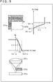
- the imaging apparatus of the present disclosure uses an imaging device 51 in which the detection sensitivity of each pixel has incident angle directivity as depicted in the upper left of FIG. 1 .
- the detection sensitivity of each pixel has incident angle directivity signifies that the light reception sensitivity characteristic according to the incident angle of incident light to a pixel is made different for each pixel.
- the light reception sensitivity need not be fully different among all pixels but may be same in some of the pixels.
- imaging targets are a set of point light sources and light is emitted in every direction from each point light source.
- an imaging target face 31 of an imaging target in the upper left of FIG. 1 includes a point light source PA to a point light source PC and the point light sources PA to PC emit a plurality of rays of light of a light intensity a to a light intensity c around.
- the imaging device 51 includes, at positions Pa to Pc thereof, pixels having incident angle directivities different from one another (hereinafter referred to as pixels Pa to Pc).
- rays of light of a same light intensity emitted from the same point light source enter pixels of the imaging device 51.
- rays of light of the light intensity a emitted from the point light source PA individually enter the pixels Pa to Pc of the imaging device 51.
- rays of light emitted from a same point light source enter the pixels at incident angles different from one another.
- rays of light of the point light source PA enter the pixels Pa to Pc at incident angles different from one another.
- the incident angle directivities of the pixels Pa to Pc are different from one another, rays of light of a same light intensity emitted from the same point light source are detected with sensitivities different among the different pixels.
- the rays of light of the same light intensity are detected at signal levels different from one another by the different pixels.
- the detection signal level in regard to a ray of light of the light intensity a from the point light source PA has different values from one another at the pixels Pa to Pc.
- the light reception sensitivity level of each pixel for a ray of light from each point light source is calculated by multiplying the light intensity of the ray of light by a coefficient indicative of a light reception sensitivity (namely, incident angle directivity) at the incident angle of the ray of light.
- the detection signal level of the pixel Pa for a ray of light from the point light source PA is calculated by multiplying the light intensity a of the ray of light of the point light source PA by a coefficient indicative of the incident angle directivity of the pixel Pa at the incident angle of the ray of light to the pixel Pa.
- the detection signal levels DA, DB, and DC at the pixels Pc, Pb, and Pa are represented by the following expressions (1) to (3), respectively.
- DA ⁇ 1 ⁇ a + ⁇ 1 ⁇ b + ⁇ 1 ⁇ c
- DB ⁇ 2 ⁇ a + ⁇ 2 ⁇ b + ⁇ 2 ⁇ c
- DC ⁇ 3 ⁇ a + ⁇ 3 ⁇ b + ⁇ 3 ⁇ c
- the coefficient ⁇ 1 is a coefficient indicative of the incident angle directivity of the pixel Pc at the incident angle of a ray of light from the point light source PA to the pixel Pc, and is set according to the incident angle. Further, ⁇ 1 ⁇ a indicates the detection signal level at the pixel Pc for the ray of light from the point light source PA.
- the coefficient ⁇ 1 is a coefficient indicative of the incident angle directivity of the pixel Pc at the incident angle of a ray of light from the point light source PB to the pixel Pc, and is set according to the incident angle. Further, ⁇ 1 ⁇ b indicates the detection signal level at the pixel Pc for the ray of light from the point light source PB.
- the coefficient ⁇ 1 is a coefficient indicative of the incident angle directivity of the pixel Pc at the incident angle of a ray of light y from the point light source PC to the pixel Pc, and is set according to the incident angle. Further, ⁇ 1 ⁇ c indicates the detection signal level at the pixel Pc for the ray of light from the point light source PC.
- the detection signal level DA of the pixel Pa is calculated by the product sum of the light intensities a, b, and c of light rays at the pixel Pc from the point light sources PA, PB, and PC and the coefficients ⁇ 1, ⁇ 1, and ⁇ 1 indicative of the incident angle directivities according to the respective incident angles.
- the detection signal level DB of the pixel Pb is calculated by the product sum of the light intensities a, b, and c of rays of light at the pixel Pb from the point light sources PA, PB, and PC and the coefficients ⁇ 2, ⁇ 2, and ⁇ 2 indicative of the incident angle directivities according to the respective incident angles as indicated by the expression (2).
- the detection signal level DC of the pixel Pc is calculated by the product sum of the light intensities a, b, and c of rays of light at the pixel Pa from the point light sources PA, PB, and PC and the coefficients ⁇ 2, ⁇ 2, and ⁇ 2 indicative of the incident angle directivities according to the respective incident angles as indicated by the expression (3).
- the detection signal levels DA, DB, and DC at the pixels Pa, Pb, and Pc are mixtures of the light intensities a, b, and c of rays of light emitted from the point light sources PA, PB, and PC as indicated by the expressions (1) to (3). Accordingly, as indicated at the upper right of FIG. 1 , the detection signal level at the imaging device 51 is different from the light intensities of the point light sources on the imaging target face 31. Accordingly, the image obtained by the imaging device 51 is different from an image in which an image of the imaging target face 31 is formed.
- the light intensities a to c of light rays of the point light sources PA to PC are found. Then, by arranging the pixels having pixel values according to the calculated light intensities a to c in accordance with the arrangement (relative positions) of the point light sources PA to PC, a restoration image in which the image of the imaging target face 31 is formed as depicted in the lower right of FIG. 1 is restored.
- coefficient set an aggregation of coefficients (for example, the coefficients ⁇ 1, ⁇ 1, and ⁇ 1) for each expression configuring simultaneous equations.
- coefficient set group an aggregation of a plurality of coefficient sets corresponding to a plurality of expressions included in simultaneous equations (for example, the coefficient set ⁇ 1, ⁇ 1, and ⁇ 1, coefficient set ⁇ 2, ⁇ 2, and ⁇ 2 and coefficient set ⁇ 3, ⁇ 3, and ⁇ 3) is hereinafter referred to as coefficient set group.
- an imaging apparatus that includes, as essential components, the imaging device 51 having an incident angle directivity at each pixel without the necessity for an imaging lens, a pinhole and the optical filter disclosed in PTL 1 and NPL 1 (hereinafter referred to as patent document and so forth).
- an imaging lens, a pinhole and the optical filter disclosed in the patent document and so forth do not become essential components, reduction in height of the imaging apparatus, namely, in thickness of the configuration for implementing an imaging function in the entering direction of light, becomes possible.
- the essential component is only the imaging device 51, it is possible to improve the degree of freedom in design.
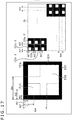
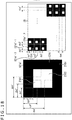
- a conventional imaging apparatus that uses an imaging lens it is necessary to arrange a plurality of pixels of an imaging device in a two-dimensional array in accordance with a position at which an image of an imaging target is to be formed by the imaging lens, an imaging apparatus that uses the imaging device 51 does not have the necessity. Therefore, the degree of freedom in arrangement of pixels is improved, and it is possible to freely arrange pixels, for example, within a range into which light from an imaging target enters. Accordingly, it is possible to arrange pixels in a circular range, to arrange pixels in a hollow square region or to arrange pixels dispersedly in a plurality of regions.
- FIGS. 2 to 25 An example of a basic configuration of the imaging apparatus of the present disclosure is described with reference to FIGS. 2 to 25 .
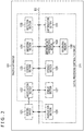
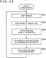
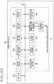
- FIG. 2 is a block diagram depicting an example of a configuration of the imaging apparatus 101 that is a basic imaging apparatus to which the technology of the present disclosure is applied.
- the imaging apparatus 101 includes an imaging device 121, a restoration section 122, a control section 123, an inputting section 124, a detection section 125, an association section 126, a display section 127, a storage section 128, a recording and reproduction section 129, a recording medium 130, and a communication section 131.
- a signal processing controlling section 111 that performs signal processing, control of the imaging apparatus 101, and so forth includes the restoration section 122, the control section 123, the inputting section 124, the detection section 125, the association section 126, the display section 127, the storage section 128, the recording and reproduction section 129, the recording medium 130, and the communication section 131. It is to be noted that the imaging apparatus 101 does not include any imaging lens (imaging lens-free).
- the imaging device 121, the restoration section 122, the control section 123, the inputting section 124, the detection section 125, the association section 126, the display section 127, the storage section 128, the recording and reproduction section 129, and the communication section 131 are connected to one another through a bus B1 such that they perform transmission, reception, and so forth of data through the bus B1.
- a bus B1 such that they perform transmission, reception, and so forth of data through the bus B1.
- description of the bus B1 in the case where the components of the imaging apparatus 101 perform transmission, reception, and so forth of data through the bus B1 is omitted.
- the inputting section 124 data supplies to the control section 123 through the bus B1
- this is described such that the inputting section 124 supplies data to the control section 123.
- the imaging device 121 corresponds to the imaging device 51 described hereinabove with reference to FIG. 1 and is an imaging device that includes pixels having an incident angle directivity and outputs an image including a detection signal indicative of a detection signal level according to a light amount of incident light to the restoration section 122 or the bus B1.
- the imaging device 121 may be, in a basic structure, an imaging device similar to an imaging device of a general, for example, CMOS (Complementary Metal Oxide Semiconductor) image sensor or the like.
- the imaging device 121 is different in configuration of pixels configuring a pixel array from a general one and has a configuration that pixels have an incident angle directivity as hereinafter described, for example, with reference to FIGS. 3 to 5 .
- the imaging device 121 is different in (changes) light reception sensitivity in response to the incident angle of incident light for each pixel and has an incident angle directivity for an incident angle of incident light in a unit of a pixel.
- an image outputted from the imaging device 121 is an image including detection signals in which an image of an imaging target is not formed as depicted, for example, in the upper right of FIG. 1 described hereinabove, the imaging target cannot be recognized visually.
- a detection image including detection signals outputted from the imaging device 121 is an aggregation of pixel signals, it is an image on which the imaging target cannot be recognized, even if the user sees, by the user (image on which the imaging target cannot be visually recognized).
- detection image an image including a detection signal where an image of an imaging target is not formed as depicted in the upper right of FIG. 1 , namely, an image captured by the imaging device 121, is referred to as detection image.
- the imaging device 121 may not be configured as a pixel array and, for example, may be configured as a line sensor. Further, the incident angle directivity need not be all different in a unit of a pixel, but some pixels may have a same incident angle directivity.
- the restoration section 122 acquires, from the storage section 128, a coefficient set group corresponding to an imaging target distance corresponding to a distance from the imaging device 51 to the imaging target face 31 (imaging target face corresponding to a restoration image) in FIG. 1 and corresponding to the coefficients ⁇ 1 to ⁇ 3, ⁇ 1 to ⁇ 3, and ⁇ 1 to ⁇ 3 described hereinabove. Further, the restoration section 122 creates such simultaneous equations as indicated by the expressions (1) to (3) given hereinabove using detection signal levels of the pixels of a detection image outputted from the imaging device 121 and the acquired coefficient set group.
- the restoration section 122 solves the created simultaneous equations to calculate pixel values of the pixels configuring the image in which an image of the imaging target depicted at the right lower portion of FIG. 1 is formed. Consequently, an image in which the imaging target can be recognized by visual observation of the user (imaging target can be visually recognized) is restored from the detection image.
- the image restored from the detection image is referred to as restoration image.
- the imaging device 121 has sensitivity only to light other than that in a visually recognizable frequency band such as ultraviolet light
- the restored image does not become an image on which an imaging target can be identified as in an ordinary image
- restoration image is referred to as restoration image.
- a restoration image that is an image in a state in which an image of an imaging target is formed but is an image before color separation such as a demosaic process or a synchronization process is referred to as RAW image
- a detection image captured by the imaging device 121 is distinguished not as a RAW image although it is an image according to an array of color filters.
- the number of pixels of the imaging device 121 and the pixel number of pixels that configure a restoration image need not necessary be equal to each other.
- the restoration section 122 performs, for a restoration image, a demosaic process, ⁇ correction, white balance adjustment, a conversion process into a predetermined compression format and so forth as occasion demands. Then, the restoration section 122 outputs the restoration image to the bus B1.
- the control section 123 includes, for example, various types of processors and controls the components of the imaging apparatus 101.
- the inputting section 124 includes inputting devices for performing an operation of the imaging apparatus 101 and inputting of data to be used for processing and so forth (for example, keys, switches, buttons, dials, a touch panel, a remote controller, and so forth).
- the inputting section 124 outputs an operation signal, inputted data, and so forth to the bus B1.
- the detection section 125 includes various types of sensors and so forth to be used for detection of a state of the imaging apparatus 101 and an imaging target.
- the detection section 125 includes an acceleration sensor and a gyro sensor for detecting the posture or a movement of the imaging apparatus 101, a position detection sensor for detecting the position of the imaging apparatus 101 (for example, a GNSS (Global Navigation Satellite System) receiver and so forth), a distance measurement sensor for detecting an imaging target distance and so forth.
- the detection section 125 outputs a signal representative of a result of the detection to the bus B1.
- the association section 126 performs association between a detection image obtained by the imaging device 121 and metadata corresponding to the detection image.
- the metadata includes, for example, a coefficient set group, an imaging target distance and so forth for restoring a restoration image using a detection image that is a target.
- the method for associating a detection image and metadata with each other is not specifically restricted if it can specify a corresponding relation between the detection image and the metadata.
- the detection image and the metadata can be associated with each other.
- the display section 127 is configured, for example, from a display and performs display of various kinds of information (for example, a restoration image or the like). It is to be noted that also it is possible to configure the display section 127 such that it includes a sound outputting section such as a speaker to perform outputting of sound.
- the storage section 128 includes one or more storage devices such as a ROM (Read Only Memory), a RAM (Random Access Memory) and a flash memory and stores a program, data and so forth used, for example, in processing of the imaging apparatus 101.
- the storage section 128 stores coefficient set groups corresponding to the coefficients ⁇ 1 to ⁇ 3, ⁇ 1 to ⁇ 3, and ⁇ 1 to ⁇ 3 described hereinabove in an associated relation with various imaging target distances. More particularly, for each of imaging target faces 31 at different imaging target distances, the storage section 128 stores a coefficient set group including coefficients for the pixels 121a of the imaging device 121 with respect to each point light source set on the imaging target face 31.
- the recording and reproduction section 129 performs recording of data into the recording medium 130 and reproduction (reading out) of data recorded in the recording medium 130.
- the recording and reproduction section 129 records a restoration image into the recording medium 130 and reads out the restoration image from the recording medium 130.
- the recording and reproduction section 129 records a detection image and corresponding metadata into the recording medium 130 and reads out them from the recording medium 130.
- the recording medium 130 is one or a combination of, for example, an HDD (Hard Disk Drive), an SSD (Solid State Drive), a magnetic disk, an optical disk, a magneto-optical disk, a semiconductor memory, and so forth.
- an HDD Hard Disk Drive
- SSD Solid State Drive
- magnetic disk an optical disk
- optical disk an optical disk
- magneto-optical disk a magneto-optical disk
- semiconductor memory and so forth.
- the communication section 131 performs communication with a different apparatus (for example, a different imaging apparatus, a signal processing apparatus or the like) by a predetermined communication method. It is to be noted that the communication method of the communication section 131 may be any of wired communication and wireless communication. Also it is possible for the communication section 131 to be made ready for a plurality of communication methods.
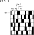
- FIGS. 3 and 4 a first example of a configuration of the imaging device 121 of the imaging apparatus 101 of FIG. 2 is described with reference to FIGS. 3 and 4 .
- FIG. 3 depicts a front elevational view of part of the pixel array section of the imaging device 121. It is to be noted that, although FIG. 3 depicts an example of a case in which the number of pixels of the pixel array section is vertical six pixels ⁇ horizontal six pixels, the pixel number of the pixel array section is not limited to this.
- a light shielding film 121b that is one of modulation elements is provided for each pixel 121a such that it covers part of a light reception region (light reception face) of the photodiode of the pixel 121a, and incident light entering each pixel 121a is optically modulated in response to an incident angle. Then, for example, by providing the light shielding film 121b for a range different for each pixel 121a, the light reception sensitivity to the incident angle of incident light becomes different for each pixel 121a, and the pixels 121a have incident angle directivities different from one another.
- the pixel 121a-1 and the pixel 121a-2 are different from each other in range over which the light reception region of the photodiode is shielded by the light shielding film 121b-1 and the light shielding film 121b-2 (different in at least one of the shielded region (position) and the shielded area).
- the light shielding film 121b-1 is provided such that it shields a left side portion of the light reception region of the photodiode with a predetermined width.
- the light shielding film 121b-2 is provided such that it shields a right side portion of the light reception region with a predetermined width.
- the width over which the light reception region of the photodiode is shielded by the light shielding film 121b-1 and the width over which the light reception region of the photodiode is shielded by the light shielding film 121b-2 may be different from each other or may be equal to each other.
- the light shielding films 121b are arrayed at random in the pixel array such that the pixels are shielded over the ranges of the light reception regions different from one another.
- the area of the light shielding film 121b is preferably made an area of such a degree that a desired light amount can be assured, and for example, the area may be restricted such that it is approximately 3/4 the light reception region in the maximum. This makes it possible to assure a light amount equal to or greater than a desired amount.
- a non-shielded range of a width corresponding to the wavelength of light to be received is provided for each pixel, then it is possible to receive a minimal light amount. That is, for example, in the case of a B pixel (blue pixel), although the wavelength is approximately 500 nm, it is possible to receive a minimal light amount if it is not shielded to an extent of the width corresponding to the wavelength or more.
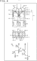
- An upper stage of FIG. 4 is a side elevational sectional view of the first configuration example of the imaging device 121
- a middle stage of FIG. 4 is a top plan view of the first configuration example of the imaging device 121.
- the side elevational sectional view at the upper stage of FIG. 4 is an AB cross section at the middle stage of FIG. 4 .
- a lower stage of FIG. 4 depicts an example of a circuit configuration of the imaging device 121.
- the pixels 121a-1 and 121a-2 adjacent each other have a wiring layer Z12 in a lowermost layer in the figure and a photoelectric conversion layer Z11 is provided on the wiring layer Z12 such that they are configured as those of the so-called backside illumination type.
- each of them is referred to merely as pixel 121a with the number at the end of the reference sign omitted.
- reference signs with the number at the end of the reference sign omitted.
- FIG. 4 only a side elevational view and a top plan view for two pixels configuring the pixel array of the imaging device 121 are depicted, and needless to say, although a greater number of pixels 121a are arranged, illustration of them is omitted.
- the pixels 121a-1 and 121a-2 include photodiodes 121e-1 and 121e-2 in the photoelectric conversion layer Z11, respectively. Further, on the photodiodes 121e-1 and 121e-2, on-chip lenses 121c-1 and 121c-2 and color filters 121d-1 and 121d-2 are stacked from above, respectively.
- the on-chip lenses 121c-1 and 121c-2 condense incident light on the photodiodes 121e-1 and 121e-2.
- the color filters 121d-1 and 121d-2 are optical filters each of which transmits light of a specific wavelength such as, for example, red, green, blue, infrared, or white. It is to be noted that, in the case of white, the color filters 121d-1 and 121d-2 may be transparent filters or may not be provided.
- light shielding films 121g-1 to 121g-3 are formed and suppress incident light L from entering an adjacent pixel as depicted, for example, in FIG. 4 thereby to suppress occurrence of crosstalk.
- the light shielding films 121b-1 and 121b-2 shield part of a light reception face S as viewed from above.
- the range to be shielded need not be differ among all pixels 121a of the imaging device 121, and pixels 121a that are shielded over a same range may exist partly.
- the light shielding film 121b-1 and the light shielding film 121g-1 are connected to each other and are configured in an L shape as viewed from the side.
- the light shielding film 121b-2 and the light shielding film 121g-2 are connected to each other and are configured in an L shape as viewed from the side.
- the light shielding film 121b-1, the light shielding film 121b-2, and the light shielding films 121g-1 to 121g-3 include metal and, for example, include tungsten (W), aluminum (Al) or an alloy of Al and copper (Cu).
- the light shielding film 121b-1, the light shielding film 121b-2, and the light shielding films 121g-1 to 121g-3 may be formed simultaneously from a metal same as that of wires by a process same as a process by which the wires are formed in a semiconductor process. It is to be noted that the film thicknesses of the light shielding film 121b-1, the light shielding film 121b-2, and the light shielding films 121g-1 to 121g-3 may not be a same thickness depending upon the position.
- the pixel 121a includes a photodiode 161 (corresponding to the photodiode 121e), a transfer transistor 162, an FD (Floating Diffusion) portion 163, a selection transistor 164, an amplification transistor 165 and a reset transistor 166 and is connected to a current source 168 through a vertical signal line 167.
- a photodiode 161 corresponding to the photodiode 121e
- FD Floating Diffusion
- the photodiode 161 is grounded at the anode electrode thereof and connected at the cathode electrode thereof to the gate electrode of the amplification transistor 165 through the transfer transistor 162.
- the transfer transistor 162 is driven in accordance with a transfer signal TG. If the transfer signal TG supplied to the gate electrode of the transfer transistor 162 becomes the high level, then the transfer transistor 162 is turned on. Consequently, charge accumulated in the photodiode 161 is transferred to the FD portion 163 through the transfer transistor 162.
- the amplification transistor 165 serves as an inputting portion of a source follower circuit that is a reading out circuit for reading out a signal obtained by photoelectric conversion by the photodiode 161, and outputs a pixel signal of a level according to the charge accumulated in the FD portion 163 to the vertical signal line 167.
- the amplification transistor 165 is connected at the drain terminal thereof to the power supply VDD and connected at the source terminal thereof to the vertical signal line 167 through the selection transistor 164 such that it cooperates with the current source 168 connected at one end of the vertical signal line 167 to configure a source follower.
- the FD portion 163 is a floating diffusion region having charge capacitance C1 provided between the transfer transistor 162 and the amplification transistor 165 and temporarily accumulates charge transferred from the photodiode 161 through the transfer transistor 162.
- the FD portion 163 is a charge detection portion for converting charge into a voltage, and the charge accumulated in the FD portion 163 is converted into a voltage by the amplification transistor 165.
- the selection transistor 164 is driven in accordance with a selection signal SEL such that, when the selection signal SEL supplied to the gate electrode thereof becomes the high level, then the selection transistor 164 is turned on to connect the amplification transistor 165 and the vertical signal line 167 to each other.
- the reset transistor 166 is driven in accordance with a reset signal RST. For example, if the reset signal RST supplied to the gate electrode of the reset transistor 166 becomes the high level, then the reset transistor 166 is turned on and discharges charge accumulated in the FD portion 163 to the power supply VDD to reset the FD portion 163.
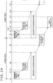
- the pixel circuit depicted at the lower stage of FIG. 4 operates in the following manner.
- the reset transistor 166 and the transfer transistor 162 are turned off to enter an exposure period, within which charge according to the light amount of incident light is accumulated by the photodiode 161.
- the reset transistor 166 is turned on to reset the FD portion 163, whereafter the reset transistor 166 is turned off.
- the FD portion 163 is set to a reference potential.
- the potential of the FD portion 163 in the reset state is outputted as a reference potential from the amplification transistor 165.
- the transfer transistor 162 is turned on and charge accumulated in the photodiode 161 is transferred to the FD portion 163.
- the potential of the FD portion 163 to which the charge of the photodiode is transferred is outputted as a signal potential from the amplification transistor 165.
- a signal when the reference potential is subtracted from the signal potential by CDS is outputted as a detection signal (pixel signal) of the pixel 121a.
- This value of the detection signal (output pixel value) is modulated in accordance with the incident angle of incident light from the imaging target and differs in characteristic (directivity) depending upon the incident angle (has an incident angle directivity).
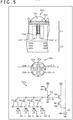
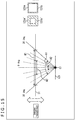
- FIG. 5 is a view depicting a second example of a configuration of the imaging device 121.
- a side elevational sectional view of a pixel 121a of the imaging device 121 of the second example of a configuration is depicted, and at a middle stage of FIG. 5 , a top plan view of the imaging device 121 is depicted.
- the side elevational view at the upper stage of FIG. 5 depicts an AB cross section at the middle stage of FIG. 5 .
- a lower stage of FIG. 5 depicts an example of a circuit configuration of the imaging device 121.
- the imaging device 121 of FIG. 5 is different in configuration from the imaging device 121 of FIG. 4 in that four photodiodes 121f-1 to 121f-4 are formed on one pixel 121a and a light shielding film 121g is formed in a region that separates the photodiodes 121f-1 to 121f-4 from each other.
- the light shielding film 121g is formed in a "+" shape as viewed from above. It is to be noted that such common components as described above are denoted by the same reference signs to those of FIG. 4 and detailed description of them is omitted.
- the photodiodes 121f-1 to 121f-4 are separated from each other by the light shielding film 121g to prevent occurrence of electric and optical crosstalk between the photodiodes 121f-1 to 121f-4.
- the light shielding film 121g of FIG. 5 is provided to prevent crosstalk similarly to the light shielding film 121g of the imaging device 121 of FIG. 4 but not to provide an incident angle directivity.
- one FD portion 163 is shared by the four photodiodes 121f-1 to 121f-4.
- a lower stage of FIG. 5 depicts an example of a circuit configuration in which the one FD portion 163 is shared by the four photodiodes 121f-1 to 121f-4. It is to be noted that description of the same components at the lower stage of FIG. 5 as those at the lower stage of FIG. 4 is omitted.
- the circuit configuration is different from the circuit configuration at the lower stage of FIG. 4 in that, in place of the photodiode 161 (corresponding to the photodiode 121e at the upper stage of FIG. 4 ) and the transfer transistor 162, photodiodes 161-1 to 161-4 (corresponding to the photodiodes 121f-1 to 121f-4 at the upper stage of FIG. 5 ) and transfer transistors 162-1 to 162-4 are provided and the FD portion 163 is shared.
- charge accumulated in the photodiodes 121f-1 to 121f-4 is transferred to the common FD portion 163 provided at the connection portion between the photodiodes 121f-1 to 121f-4 and the gate electrode of the amplification transistor 165 and having a predetermined capacitance. Then, a signal according to the level of the charge held in the FD portion 163 is read out as a detection signal (pixel signal) (it is to be noted, however, that a CDS process is performed as described above).
- charge accumulated in the photodiodes 121f-1 to 121f-4 can selectively contribute in various combinations to an output of the pixel 121a, namely, to the detection signal.
- the photodiodes 121f-1 to 121f-4 such that charge can be read out from them independently of each other and making the photodiodes 121f-1 to 121f-4 that contribute to the output (degrees with which the photodiodes 121f-1 to 121f-4 contribute to the output) different from each other, a different incident angle directivity can be obtained.
- an incident angle directivity in the leftward and rightward direction can be obtained.
- an incident angle directivity in the upward and downward direction can be obtained.
- a signal obtained based on charge selectively read out independently from the four photodiodes 121f-1 to 121f-4 becomes a detection signal corresponding to one pixel configuring a detection image.
- each photodiode 121f can be implemented not only, for example, by whether or not charge (detection value) of each photodiode 121f is to be transferred to the FD portion 163 but also by resetting the charge accumulated in the photodiodes 121f before the charge is transferred to the FD portion 163 using an electronic shutter function. For example, if the charge of a photodiode 121f is reset immediately before transfer to the FD portion 163, then the photodiode 121f does not at all contribute to the detection signal. On the other hand, by providing a period of time between resetting of charge of a photodiode 121f and transfer of the charge to the FD portion 163, the photodiode 121f partially contributes to the detection signal.
- the imaging device 121 of FIG. 5 by changing the combination of those of the four photodiodes 121f-1 to 121f-4 that are to be used for a detection signal, a different incident angle directivity can be provided to each pixel. Further, the detection signal outputted from each pixel 121a of the imaging device 121 of FIG. 5 has a value (output pixel value) modulated in response to the incident angle of incident light from an imaging target, and the characteristic (directivity) differs (has a different incident angle directivity) depending upon the incident angle.
- pixel output unit a unit with which a detection signal corresponding to one pixel of a detection image is hereinafter referred to as pixel output unit.
- the pixel output unit includes at least one or more photodiodes, and normally, each pixel 121a of the imaging device 121 corresponds to one pixel output unit.
- each one pixel output unit includes one photodiode 121e.
- one pixel output unit includes one photodiode 121e.
- the incident angle directivities of the pixel output units can be made different from each other.
- the incident light to each pixel 121a is optically modulated using the light shielding film 121b, and as a result, from signals outputted from the photodiodes 121e of the pixels 121a, a detection signal for one pixel of the detection image that reflects an incident angle directivity is obtained.
- the imaging device 121 of FIG. 4 the imaging device 121 of FIG.
- each of the pixel output units includes one photodiode 121e and a characteristic (incident angle directivity) of incident light from an imaging target to the incident angle is set for each pixel output unit.
- one pixel output unit includes the four photodiodes 121e.
- one pixel output unit includes the four photodiodes 121f.
- an individual pixel output unit is not configured from a single substance of each photodiode 121e.
- the incident angle directivity for each pixel output unit becomes different.
- a range that does not contribute to an output (detection signal) among the four photodiodes 121f-1 to 121f-4 functions similarly to the shielded region.
- a detection signal for one pixel of a detection image that reflects an incident angle directivity is obtained.
- the imaging device 121 of FIG. 5 the imaging device 121 of FIG.
- each pixel output unit includes a plurality of photodiodes (for example, the photodiodes 121f-1 to 121f-4) and, by making (the degree of) the photodiodes that contribute to an output different, characteristics (incident angle directivities) of the pixel output units of incident light from an imaging target to the incident angle become different from each other.
- the detection signal is not a signal obtained by optical modulation.
- the photodiode 121f that does not contribute to a detection signal is referred to also as photodiode 121f that does not contribute to a pixel output unit or an output.
- FIG. 5 depicts an example in which the light reception face of a pixel output unit (pixel 121a) is equally divided into four and photodiodes 121f having a light reception face of an equal magnitude are arranged in each pixel output unit, namely, an example in which a photodiode is equally divided into four, the dividing number and the dividing position of a photodiode can be set arbitrarily.
- a photodiode need not necessarily be divided equally, and the dividing position of the photodiode may be made different for each pixel output unit. This makes it possible to make the incident angle directivity different in different pixel output units even if the photodiodes 121f at same positions are made contribute to an output between a plurality of pixel output units. Further, for example, by making the dividing number different between different pixel output units, it becomes possible to set the incident angle directivity more freely. Furthermore, for example, both the dividing number and the dividing position may be made different between different pixel output units.
- both the imaging device 121 of FIG. 4 and the imaging device 121 of FIG. 5 are configured such that each pixel output unit can set an incident angle directivity independently.
- the imaging apparatus disclosed in NPL 1, PTL 1, and PTL 2 described hereinabove are not configured such that each pixel output unit of an imaging device can set an incident angle directivity independently. It is to be noted that, in the imaging device 121 of FIG. 4 , the incident angle directivity of each pixel output unit is set by the light shielding film 121b upon manufacturing. On the other hand, in the imaging device 121 of FIG.
- the incident angle directivity of each pixel output unit can be set at the time of use (for example, at the time of imaging). It is to be noted that both the imaging device 121 of FIG. 4 and the imaging device 121 of FIG. 5 need not have a configuration for causing all pixel output units to have an incident angle directivity.
- each pixel of an imaging device usually corresponds to one pixel output unit
- one pixel output unit sometimes includes a plurality of pixels. The following description is given assuming that, unless otherwise specified, each pixel of an imaging device corresponds to one pixel output unit.
- each pixel of the imaging device 121 is generated, for example, by such a principle as depicted in FIG. 6 . It is to be noted that that an upper left portion and an upper right portion of FIG. 6 are views illustrating a generation principle of an incident angle directivity in the imaging device 121 of FIG. 4 , and a left lower portion and a right lower portion of FIG. 6 are views illustrating a generation principle of an incident angle directivity in the imaging device 121 of FIG. 5 .
- Each of pixels at the upper left portion and the upper right portion of FIG. 6 includes one photodiode 121e.
- each of pixels at the left lower portion and the right lower portion of FIG. 6 includes two photodiodes 121f. It is to be noted that, although an example in which one pixel includes two photodiodes 121f is depicted here, this is for the convenience of description, and the number of photodiodes 121f provided in one pixel may be any other number.
- the light shielding film 121b-11 is formed such that it shields a right half of the light reception face of the photodiode 121e-11. Meanwhile, in the pixel at the upper right portion of FIG. 6 , the light shielding film 121b-12 is formed such that it shields a left half of the light reception face of the photodiode 121e-12. It is to be noted that a chain line in the figure is an auxiliary line that passes the center of the light reception face of the photodiode 121e in the horizontal direction and is perpendicular to the light reception face.
- the pixel at the upper left portion of FIG. 6 has an incident angle directivity that is high in light reception sensitivity to incident light from the upper right of the figure but is low in light reception sensitivity to incident light from the upper left.
- the pixel at the upper right portion of FIG. 6 incident light from the upper right direction having an incident angle ⁇ 1 is less liable to be received by the left half range of the photodiode 121e-12 that is shielded by the light shielding film 121b-12.
- incident light from the upper left direction having an incident angle ⁇ 2 is liable to be received by the right half range of the photodiode 121e-12 that is not shielded by the light shielding film 121b-12.
- the pixel at the upper right portion of FIG. 6 has an incident angle directivity that it is low in light reception sensitivity to incident light from the upper right of the figure but is high in light reception sensitivity to incident light from the upper left.
- the pixel at the lower left portion of FIG. 6 is configured such that it has photodiodes 121f-11 and 121f-12 on the left and right in the figure and, by reading a detection signal of any one of them, an incident angle directivity is provided without the provision of the light shielding film 121b.
- a pixel includes two photodiodes 121f-13 and 121f-14 like the pixel at the lower right portion of FIG. 6
- an incident angle directivity similar to that of the pixel at the upper right portion of FIG. 6 can be obtained.
- incident light from the upper right direction having the incident angle ⁇ 1 enters the photodiode 121f-13, since a signal is not read out from the photodiode 121f-13, this does not contribute to a detection signal to be outputted from this pixel.
- the pixels at the upper portion of FIG. 6 indicate examples in which a range that is shielded and a range that is not shielded are separated at a central position of the pixel (light reception face of the photodiode 121e) in the horizontal direction, the ranges may be separated at a different position.
- the pixels at the lower portion of FIG. 6 indicate examples in which the two photodiodes 121f are separated at a central position of the pixel in the horizontal direction, they may be separated at a different position.
- a graph at an upper stage of FIG. 7 indicates incident angle directivities of pixels at middle and lower stages of FIG. 7 .
- the axis of abscissa indicates the incident angle ⁇ and the axis of ordinate indicates the detection signal level.
- the incident angle ⁇ is defined such that it is 0 degrees where the direction of incident light coincides with a chain line on the left side at the middle stage of FIG. 7 and the incident angle ⁇ 21 side on the left side at the middle stage of FIG. 7 is the positive direction while the incident angle ⁇ 22 side on the right side at the middle stage of FIG. 7 is the negative direction.
- incident light entering the on-chip lens 121c from the upper right has an incident angle greater than that of incident light entering from the upper left.
- the incident angle ⁇ increases (increases in the positive direction) as the advancing direction of incident light is inclined to the left and decreases (increases in the negative direction) as the advancing direction of incident light is inclined to the right.
- the pixel at the left portion at the middle stage of FIG. 7 is configured such that an on-chip lens 121c-11 that condenses incident light and a color filter 121d-11 that passes light of a predetermined wavelength are added to the pixel at the left portion at the upper stage of FIG. 6 .
- the on-chip lens 121c-11, color filter 121d-11, light shielding film 121b-11, and photodiode 121e-11 are stacked in order from the entering direction of light in the upper portion in the figure.
- the pixel at the right portion at the middle stage of FIG. 7 , the pixel at the left portion at the lower stage of FIG. 7 and the pixel at the right portion at the lower state of FIG. 7 are configured such that the on-chip lens 121c-11 and the color filter 121d-11 or an on-chip lens 121c-12 and a color filter 121d-12 are added to the pixel at the right portion at the upper stage of FIG. 6 , the pixel at the left portion at the lower stage of FIG. 6 and the pixel at the right portion at the lower stage of FIG. 6 , respectively.
- the detection signal level (light reception sensitivity) of the photodiode 121e-11 changes in response to the incident angle ⁇ of incident light as indicated by a solid line waveform at the upper state of FIG. 7 .
- the detection signal level of the photodiode 121e-11 increases because light is condensed to a range in which the light shielding film 121b-11 is not provided.
- the detection signal level of the photodiode 121e-11 decreases because light is condensed to a range in which the light shielding film 121b-11 is provided.
- the detection signal level (light reception sensitivity) of the photodiode 121e-12 changes in response to the incident angle ⁇ of incident light as indicated by a broken line waveform at the upper stage of FIG. 7 .
- the detection signal level of the photodiode 121e-12 decreases because light is condensed to a range in which the light shielding film 121b-12 is provided.
- the detection signal level of the photodiode 121e-12 increases because light enters a range in which the light shielding film 121b-12 is not provided.
- the incident angle directivity is a characteristic of the light reception sensitivity of each pixel according to the incident angle ⁇ as described hereinabove, it can be considered that, in regard to the pixels at the middle stage of FIG. 7 , this is a characteristic of the light shielding value according to the incident angle ⁇ .
- the light shielding film 121b shields incident light in a specific direction at a high level, it cannot sufficiently shield incident light from any other direction.
- the change of the level at which incident light can be shielded gives rise to a different detection signal level according to the incident angle ⁇ as depicted at the upper stage of FIG. 7 .
- a direction in which incident light to each pixel in a direction in which it can be shielded at the highest level is defined as a light shielding direction of the pixel, then that pixels have incident angle directivities different from each other in a unit of a pixel is, in other words, that different pixels have light shielding directions different from each other in a unit of a pixel.
- the detection signal level increases because light is condensed to a range of the photodiode 121f-11 from which a signal is read out.
- the detection signal level decreases because light is condensed to a range of the photodiode 121f-12 from which a signal is not read out.
- an incident angle directivity similar to that of the pixel at the right portion at the middle stage of FIG. 7 can be obtained.
- the detection signal level in a unit of a pixel decreases because light is condensed to a range of the photodiode 121f-13 that does not contribute to an output (detection signal).
- the detection signal level in a unit of a pixel increases because light is condensed to a range of the photodiode 121f-14 that contributes to an output (detection signal).
- the on-chip lens 121c is an essential component for each pixel.
- the incident angle directivity preferably has a high degree of randomness in a unit of a pixel.
- the expressions (1) to (3) given hereinabove or expressions (4) to (6) hereinafter described may become a same expression, and as a result, there is the possibility that the number of expressions may become insufficient for a number of unknowns that become solutions to the simultaneous equations and it may become impossible to calculate pixel values that configure a restoration image.
- the light shielding film 121b of each pixel 121a of the imaging device 121 is configured such that it shields the entire light reception face in the vertical direction but changes the light shielding width or position in the horizontal direction.
- the entire light reception face is shielded in the horizontal direction such that the width (weight) or position in the vertical direction is changed to provide an incident angle directivity to each pixel 121a.
- a light shielding film 121b that shields the entire light reception face of a pixel 121a in the vertical direction and shields the light reception face with a predetermined width in the horizontal direction as in the example of FIG. 3 is referred to as light shielding film 121b of the horizontal belt type.
- a light shielding film 121b that shields the entire light reception face of a pixel 121a in the horizontal direction and shields the light reception face at a predetermined height in the vertical direction is referred to as light shielding film 121b of the vertical belt type.
- light shielding films 121b of the vertical belt type and the horizontal belt type may be combined such that an L-shaped light shielding film 121b is provided for each of pixels, for example, of the Bayer array.
- a black range represents a light shielding film 121b, and unless otherwise specified, similar representation is applied also to the succeeding figures.
- L-shaped light shielding films 121b-21 to 121b-24 are provided for pixels 121a-21 and 121a-24 of G (green) pixels, a pixel 121a-22 of an R (red) pixel, and a pixel 121a-23 of a B (blue) pixel of the Bayer array, respectively.
- each pixel 121a has such an incident angle directivity as indicated at a right portion of FIG. 8 .
- a distribution of light reception sensitivities of the pixels 121a is depicted, and the axis of abscissa represents the incident angle ⁇ x in the horizontal direction (x direction) of incident light and the axis of ordinate represents the incident angle ⁇ y in the vertical direction (y direction) of incident light.
- the light reception sensitivity in a range C4 is higher than that outside the range C4; the light reception sensitivity in a range C3 is higher than that outside the range C3; the light reception sensitivity in a range C2 is higher than that outside the range C2; and the light reception sensitivity in a range C1 is higher than that outside the range C1.
- each pixel 121a indicates the highest detection signal level in regard to incident light that has the incident angle ⁇ x in the horizontal direction (x direction) and the incident angle ⁇ y in the vertical direction (y direction) that are included in the range C1. Further, the detection signal level decreases in the order of incident light whose incident angle ⁇ x and incident angle ⁇ y are included in the range C2, in the range C3, in the range C4, and in the range outside the range C4. It is to be noted that the intensity distribution of the light reception sensitivity depicted at the right portion of FIG. 8 is determined by the range shielded by the light shielding film 121b in each pixel 121a independently of the Bayer array.
- the light shielding range of a light shielding film 121b in the horizontal direction is a range from a left end portion of the pixel 121a to a position A and the light shielding range in the vertical direction is a range from an upper end portion of the pixel 121a to a position B.
- weights Wx and Wy change like those in the graph of FIG. 9 in the case where an ideal condition is satisfied.
- a coefficient of the incident angle directivity, namely, the light reception sensitivity characteristic, of each pixel 121a can be calculated. For example, a value obtained by multiplication of a weight Wx corresponding to the incident angle ⁇ x of incident light and a weight Wy corresponding to the incident angle ⁇ y of incident light from a certain point light source on the imaging target face 31 is set to the coefficient for the point light source.
- the inclination (1/2 ⁇ ) indicative of a change of the weight within a range within which the weight Wx in the horizontal direction and the weight Wy in the vertical direction are around 0.5 can be set by using on-chip lenses 121c having different focal distances.
- the inclinations (1/2 ⁇ ) of the weight Wx in the horizontal direction and the weight Wy in the vertical direction are steep.
- the focal distance of an on-chip lens 121c corresponds the surface of a photodiode 121e as indicated by a broken line at the lower stage of FIG. 9
- the inclinations (1/2 ⁇ ) of the weight Wx in the horizontal direction and the weight Wy in the vertical direction are gentle.
- the focal distance of the on-chip lens 121c changes depending upon the curvature of the on-chip lens 121c. Accordingly, by making the focal distances of the on-chip lenses 121c different from each other using the on-chip lenses 121c having curvatures different from each other, different incident angle directivities, namely, different light reception sensitivity characteristics, can be obtained.
- the incident angle directivity of a pixel 121a can be adjusted by a combination of the range within which the photodiode 121e is shielded by the light shielding film 121b and the curvature of the on-chip lens 121c. It is to be noted that the curvature of the on-chip lens may be equal among all of the pixels 121a of the imaging device 121 or may be different in some of the pixels 121a.
- each pixel 121a On the basis of the position of each pixel 121a, the shape, position, and range of the light shielding film 121b of each pixel 121a, the curvature of the on-chip lens 121c, and so forth as indices representative of the incident angle directivity of each pixel 121a of the imaging device 121, such characteristics of the weight Wx and the weight Wy as depicted in the graph of FIG. 9 are set for each pixel 121a. Further, on the basis of the positional relation between a certain point light source on the imaging target face 31 at a predetermined imaging target distance and a certain pixel 121a of the imaging device 121, the incident angle of a ray of light from the point light source to the pixel 121a is calculated. Then, on the basis of the calculated incident angle and the characteristics of the weight Wx and the weight Wy of the pixel 121a, a coefficient of the pixel 121a with respect to the point light source is calculated.
- a coefficient set group of the imaging device 121 with respect to the imaging target face 31 like a coefficient set ⁇ 1, ⁇ 1, and ⁇ 1, another coefficient set ⁇ 2, ⁇ 2, and ⁇ 2 and a further coefficient set ⁇ 3, ⁇ 3, and ⁇ 3, of the expressions (1) to (3) described hereinabove can be calculated.
- the imaging target face 31 of a same imaging target distance if the number or arrangement of point light sources to be set differs, the incident angle of a ray of light from each point light source to the imaging device 121 differs. Accordingly, a plurality of coefficient set groups is sometimes required for the imaging target face 31 of a same imaging target distance. Further, it is necessary to set the incident angle directivity of each pixel 121a such that the independence of the simultaneous equations described above can be assured.
- the imaging device 121 is configured such that it does not require an optical block including an imaging lens or a pinhole
- the on-chip lens 121c is provided as described above.
- the on-chip lens 121c and the imaging lens are different in physical action from each other.
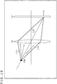
- light entering an imaging lens 152 from within diffuse light emitted from a point light source P101 is condensed at a pixel position P111 on an imaging device 151.
- the imaging lens 152 is designed such that diffuse light entering at a different angle from the point light source P101 is condensed at the pixel position P111 to form an image of the point light source P101.
- the pixel position P111 is specified by a principal ray L101 that passes the point light source P101 and the center of the imaging lens 152.
- light entering the imaging lens 152 from within diffuse light emitted from a point light source P102 different from the point light source P101 is condensed at a pixel position P112 different from the pixel position P111 on the imaging device 151.
- the imaging lens 152 is designed such that diffuse light entering at a different angle from the point light source P102 is condensed at the pixel position P112 to form an image of the point light source P102.
- This pixel position P112 is specified by a principal ray L102 that passes the point light source P102 and the center of the imaging lens 152.
- the imaging lens 152 forms images of the point light sources P101 and P102 whose principal rays are different from each other at the pixel positions P111 and P112 different from each other on the imaging device 151, respectively.
- part of diffuse light emitted from the point light source P101 enters as parallel light parallel to the principal ray L101 into the imaging lens 152.
- parallel light including rays of light between a ray L121 and another ray L122 parallel to the principal ray L101 enters the imaging lens 152.
- the parallel light entering the imaging lens 152 is condensed at the pixel position P111 on the imaging device 151.
- the imaging lens 152 is designed such that parallel light from the point light source P101 existing in the infinity is condensed at the pixel position P111 to form an image of the point light source P101.
- the imaging lens 152 has a light condensing function for introducing diffuse light from a point light source having, for example, a principal ray incident angle ⁇ 1 into a pixel (pixel output unit) P1 and introducing diffuse light from a point light source having a principal ray incident angle ⁇ 2 different from the principal ray incident angle ⁇ 1 into a pixel (pixel output unit) P2 different from the pixel P1.
- the imaging lens 152 has a light condensing function for introducing diffuse light from light sources having different incident angles of principal rays of light to a plurality of pixels (pixel output units) adjacent each other.
- light for example, from point light sources adjacent each other or from point light sources existing in the infinity and substantially adjacent each other sometimes enters the same pixel (pixel output unit).
- light passing the on-chip lens 121c enters only the light reception face of the photodiode 121e or the photodiode 121f configuring the corresponding pixel (pixel output unit).
- the on-chip lens 121c is provided for each pixel (pixel output unit) and condenses incident light entering the on-chip lens 121c itself only at the corresponding pixel (pixel output unit).
- the on-chip lens 121c does not have a condensing function for causing light from different point light sources to enter different pixels (pixel output units).
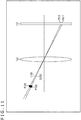
- the detection signal levels DA, DB, and DC at the pixels Pc, Pb, and Pa on the imaging device 121 are represented by expressions same as the expressions (1) to (3) given hereinabove.
- the detection signal levels at the pixels Pc, Pb, and Pa on the imaging device 121 are the detection signal levels DA, DB, and DC as depicted at a middle portion at the lower stage of FIG. 13 and similar to those described above.
- the detection signal levels DA, DB, and DC at the pixels Pa, Pb, and Pc are represented, for example, by the following expressions (4) to (6).
- the coefficient set group including the coefficient set ⁇ 11, ⁇ 11, and ⁇ 11, the coefficient set ⁇ 12, ⁇ 12, and ⁇ 12, and the coefficient set ⁇ 13, ⁇ 13, and ⁇ 13 is a coefficient set group for the imaging target face 31' corresponding to the coefficient set ⁇ 1, ⁇ 1, and ⁇ 1, the coefficient set ⁇ 2, ⁇ 2, and ⁇ 2, and the coefficient set ⁇ 3, ⁇ 3, and ⁇ 3 for the imaging target face 31.
- the light intensities a', b', and c' of rays of light from the point light sources PA', PB', and PC' of the imaging target face 31' can be found as indicated in the lower right of FIG. 13 by a method similar to that in the case where the light intensities a, b, and c of rays of light from the point light sources PA, PB, and PC of the imaging target face 31 are found.
- a restoration image of the imaging target face 31' can be restored.
- the imaging apparatus 101 of FIG. 2 by preparing a coefficient set group for each distance (imaging target distance) from the imaging device 121 to the imaging target face in advance and switching a coefficient set group for each imaging target distance to create simultaneous equations and then solving the created simultaneous equations, it is possible to obtain restoration images of imaging target faces at various imaging target distances on the basis of a single detection image. For example, by capturing and recording a detection image once and then using the recorded detection image to switch the coefficient set group in response to the distance to the imaging target face to restore a restoration image, a restoration image of an imaging target face at an arbitrary imaging target distance can be generated.
- detection signals not of all pixels but of pixels having incident angle directivities suitable for imaging of the imaging target face corresponding to the specified imaging target distance or angle of view may be used to generate a restoration image. This makes it possible to generate a restoration image using detection signals of pixels suitable for imaging of an imaging target face corresponding to the specified imaging target distance or angle of view.
- a pixel 121a shielded at portions thereof at the distance d1 from individual end portions of the four sides by the light shielding film 121b as depicted at an upper stage of FIG. 14 and a pixel 121a' shielded at portions thereof at the distance d2 (> d1) from individual end portions of the four sides by the light shielding film 121b as depicted at a lower stage of FIG. 14 are considered.
- FIG. 15 depicts an example of an incident angle of incident light from the imaging target face 31 to the central position C1 of the imaging device 121. It is to be noted that, although FIG. 15 depicts an example of the incident angle of incident light in the horizontal direction, this also applies similarly in regard to the vertical direction. Further, at a right portion of FIG. 15 , the pixels 121a and 121a' in FIG. 14 are depicted.
- the range of the incident angle of incident light from the imaging target face 31 to the pixel 121a is an angle A1 as indicated at a left portion of FIG. 15 . Accordingly, the pixel 121a can receive incident light for a width W1 in the horizontal direction of the imaging target face 31.
- the pixel 121a' of FIG. 14 is arranged at the central position C1 of the imaging device 121, since the pixel 121a' has a greater shielded range than the pixel 121a, the range of the incident angle of incident light from the imaging target face 31 to the pixel 121a' is an angle A2 ( ⁇ A1) as indicated at a left portion of FIG. 15 . Accordingly, the pixel 121a' can receive incident light for a width W2 ( ⁇ W1) in the horizontal direction of the imaging target face 31.
- the pixel 121a having a narrow light shielding range is a wide angle-of-view pixel suitable to image a wide range on the imaging target face 31
- the pixel 121a' having a wide light shielding range is a narrow angle-of-view pixel suitable to image a narrow range on the imaging target face 31.
- the wide angle-of-view pixel and the narrow angle-of-view pixel here are representations for comparison between the pixels 121a and 121a' of FIG. 14 and are not restrictive in comparison between pixels of other angles of view.
- the pixel 121a is used to restore an image I1 of FIG. 14 .
- the image I1 is an image of an angle SQ1 of view corresponding to the imaging target width W1 including an entire person H101 that is an imaging target at an upper stage of FIG. 16 .
- the pixel 121a' is used to restore an image I2 of FIG. 14 .
- the image I2 is an image of an angle SQ2 of view corresponding to the imaging target width W2 in which an area around the face of the person H101 at the upper stage of FIG. 16 is zoomed up.
- a restoration image of higher image quality can be obtained where an image of a narrower angle of view is restored.
- a right portion of FIG. 17 depicts an image of a configuration in the range ZA of the imaging device 121 of FIG. 16 .
- a left portion of FIG. 17 depicts an example of a configuration of the pixel 121a in the range ZA.
- a range indicated by black represents the light shielding film 121b, and the light shielding range of each pixel 121a is determined, for example, in accordance with a rule indicated at the left portion of FIG. 17 .
- a main light shielding portion Z101 of the left portion of FIG. 17 indicates a range shielded in common in the pixels 121a.
- the main light shielding portion Z101 has a range of a width dx1 from the left side and the right side of the pixel 121a toward the inner side of the pixel 121a and a range of a height dy1 from the upper side and the lower side of the pixel 121a toward the inner side of the pixel 121a.
- a rectangular opening Z111 that is not shielded by the light shielding film 121b is provided within a range Z102 on the inner side of the main light shielding portion Z101. Accordingly, in each pixel 121a, the range other than the opening Z111 is shielded by the light shielding film 121b.
- the openings Z111 of the pixels 121a are arranged regularly.
- the positions of the openings Z111 in the pixels 121a in the horizontal direction are same in the pixels 121a in a same vertical column.
- the positions of the openings Z111 in the pixels 121a in the vertical direction are same in the pixels 121a in a same horizontal row.
- the positions of the openings Z111 in the pixels 121a in the horizontal direction are displaced by a predetermined distance according to the positions of the pixels 121a in the horizontal direction.
- the left side of the opening Z111 moves to a position displaced by the width dx1, dx2, ..., dxn in the rightward direction from the left side of the pixel 121a.
- the distance between the width dx1 and the width dx2, the distance between the width dx2 and the width dx3, ..., and the distance between the dxn-1 and the width dxn are values given by dividing the length when the width of the opening Z111 is subtracted respectively from the width of the range Z102 in the horizontal direction by the pixel number n-1 in the horizontal direction.
- the position of the opening Z111 in the pixel 121a in the vertical direction is displaced by a predetermined distance in response to the position of the pixel 121a in the vertical direction.
- the upper side of the opening Z111 moves to a position displaced by the height dy1, dy2, ..., dyn from the upper side of the pixel 121a.
- the distance between the height dy1 and the height dy2, the distance between the height dy2 and the height dy3, ..., the distance between the height dyn-1 and the height dyn are values obtained by dividing the length when the height of the opening Z111 is subtracted from the height of the range Z102 in the vertical direction by the pixel number m-1 in the vertical direction.
- FIG. 18 depicts an example of a configuration in the range ZB of the imaging device 121 of FIG. 16 .
- a left portion of FIG. 18 depicts an example of a configuration of the pixels 121a' in the range ZB.
- a range indicated by black represents a light shielding film 121b', and the light shielding ranges of the pixels 121a' are determined, for example, in accordance with a rule indicated at a left portion of FIG. 18 .
- a main light shielding portion Z151 at a left portion of FIG. 18 is a range shielded in common in the pixels 121a'.
- the main light shielding portion Z151 is a range of a width dx1' from the left side and the right side of the pixel 121a' toward the inner side of the pixel 121a' and a range of a height dy1' from the upper side and the lower side of the pixel 121a' toward the inner side of the pixel 121a'.
- each pixel 121a' a rectangular opening Z161 that is not shielded by the light shielding film 121b' is provided in a range Z152 on the inner side of the main light shielding portion Z151. Accordingly, in each pixel 121a', the range other than the opening Z161 is shielded by the light shielding film 121b'.
- the openings Z161 of the pixels 121a' are arranged regularly similarly to the openings Z111 of the pixels 121a of FIG. 17 .
- the positions of the openings Z161 in the pixels 121a' in the horizontal direction are same in the pixels 121a' in a same vertical column.
- the positions of the openings Z161 in the pixels 121a' in the vertical direction are same in the pixels 121a' in a same horizontal row.
- the positions of the openings Z161 in the horizontal direction in the pixels 121a' are displaced by a predetermined distance in response to the position of the pixel 121a' in the horizontal direction.
- the left side of the opening Z161 moves to a position individually displaced in the rightward direction by the width dx1', dx2', ..., dzn' from the left side of the pixel 121a'.
- the distance between the width dx1' and the width dx2', the distance between the width dx2' and the width dx3', ..., the distance between the width dxn-1' and the width dxn' are values obtained by dividing the length when the width of the opening Z161 is subtracted from the width of the range Z152 in the horizontal direction by the pixel number n-1 in the horizontal direction.
- the positions of the openings Z161 in the pixels 121a' in the vertical direction are displaced by a predetermined distance according to the positions of the pixels 121a' in the vertical direction.
- the upper side of the opening Z161 moves to a position displaced by the width dy1', dy2', ..., dyn' in the downward direction from the upper side of the pixel 121a'.
- the distance between the width dy1' and the width dy2', the distance between the width dy2' and the width dy3', ..., and the distance between the dyn-1' and the width dyn' are values given by dividing the length when the height of the opening Z161 is subtracted respectively from the height of the range Z152 in the vertical direction by the pixel number m-1 in the vertical direction.
- the length when the width of the opening Z111 is subtracted from the width of the range Z102 of the pixel 121a of FIG. 17 in the horizontal direction is greater than the width when the width of the opening Z161 is subtracted from the width of the range Z152 of the pixel 121a' of FIG. 18 in the horizontal direction. Accordingly, the distance of the change of the widths dx1, dx2, ..., dxn of FIG. 17 is greater than the distance of the change of the widths dx1', dx2', ..., dxn' of FIG. 18 .
- the length when the height of the opening Z111 is subtracted from the height of the range Z102 of the pixel 121a of FIG. 17 in the vertical direction is greater than the length when the height of the opening Z161 is subtracted from the height of the range Z152 of the pixel 121a' of FIG. 18 in the vertical direction. Accordingly, the distance of the change of the heights dy1, dy2, ..., dyn of FIG. 17 is greater than the distance of the change of the heights dy1', dy2', ..., dyn' of FIG. 18 .
- the distances of the change of the positions in the horizontal direction and the vertical direction of the opening Z111 of the light shielding film 121b of the pixel 121a of FIG. 17 and the distances of the change of the positions in the horizontal direction and the vertical direction of the opening Z161 of the light shielding film 121b' of the pixel 121a' of FIG. 18 are different from each other. Then, the difference in distance becomes a distance of the imaging target resolution (angular resolute) in a restoration image. In particular, the distances of the change of the positions in the horizontal direction and the vertical direction of the opening Z161 of the light shielding film 121b' of the pixel 121a' of FIG.
- a restoration image restored using detection signals of the pixels 121a' of FIG. 18 is higher in imaging target resolution and higher in image quality than a restoration image restored using detection signals of the pixels 121a of FIG. 17 .
- an imaging device 121 including pixels of various angles of view (having various incident angle directivities) can be implemented.
- each unit U includes four pixels of a pixel 121a-W of a wide angle of view, a pixel 121a-M of a medium angle of view, a pixel 121a-N of a narrow angle of view and a pixel 121a-AN of a very narrow angle of view.
- the pixel number of all pixels 121a is X
- four coefficient set groups different from one another are used for each angle of view, and restoration images of angles of view different from one another are restored by four different kinds of simultaneous equations.
- images of intermediate angles of view among four angles of view and/or images of angles of view around the intermediate angles of view may be generated by interpolation from the images of the four angles of view, and by generating images of various angles of view seamlessly, pseudo optical zooming may be implemented.
- all wide angle-of-view pixels may be used or some of wide angle-of-view pixels may be used.
- all narrow angle-of-view pixels may be used or some of the narrow angle-of-view pixels may be used.
- the imaging device 121 performs imaging of an imaging target. Consequently, a detection signal indicative of a detection signal level according to a light amount of incident light from the imaging target is outputted from each of the pixels 121a of the imaging device 121 that have different incident angle directivities.
- the imaging device 121 supplies a detection image including the detection signals of the pixels 121a to the restoration section 122.
- the restoration section 122 calculates a coefficient to be used for restoration of an image.
- the restoration section 122 sets a distance to the imaging target face 31 that is a restoration target, namely, an imaging target distance.
- an arbitrary method can be adopted as the setting method of an imaging target distance.
- the restoration section 122 sets an imaging target distance inputted through the inputting section 124 by the user or an imaging target distance detected by the detection section 125 as the distance to the imaging target face 31 of the restoration target.
- the restoration section 122 reads out a coefficient set group associated with the set imaging target distance from the storage section 128.
- the restoration section 122 performs restoration of an image using the detection image and the coefficient.
- the restoration section 122 uses the detection signal levels of the pixels of the detection image and the coefficient set group acquired by the process at step S2 to create simultaneous equations described hereinabove with reference to the expressions (1) to (3) or the expressions (4) to (6) described hereinabove.
- the restoration section 122 solves the created simultaneous equations to calculate a light intensity of each point light source on the imaging target face 31 corresponding to the set imaging target distance.
- the restoration section 122 arranges the pixels having pixel values according to the calculated light intensities in accordance with the arrangement of the point light sources of the imaging target face 31 to generate a restoration image in which an image of the imaging target is formed.
- the imaging apparatus 101 performs various processes for the restoration image.
- the restoration section 122 performs a demosaic process, ⁇ correction, white balance adjustment, a conversion process into a predetermined compression format and so forth for the restoration image as occasion demands.
- the restoration section 122 supplies the restoration image to the display section 127 so as to be displayed or to the recording and reproduction section 129 so as to be recorded in the recording medium 130, or supplies the restoration image to a different apparatus through the communication section 131 as occasion demands.
- coefficient set groups corresponding to angles of view of the restoration image in addition to the imaging target distance may be prepared further in such a manner as described above such that a restoration image is restored using a coefficient set group according to an imaging target distance and an angle of view. It is to be noted that the resolution for an imaging target distance and an angle of view depends upon the number of coefficient set groups to be prepared.
- a detection image including detection signals of pixels having an incident angle directivity corresponding to a specified imaging target distance and angle of view from among the pixels configuring the imaging device 121 may be generated such that a restoration image is restored using this detection image.
- Such a process as just described makes it possible to restore a restoration image from a detection image suitable for an imaging target distance and an angle of view of a restoration image to be determined, and the restoration accuracy and the image quality of the restoration image are improved.
- an image corresponding to a specified imaging target distance and angle of view is an example corresponding, for example, to the angle SQ1 of view in FIG.
- the imaging apparatus 101 that includes, as an essential component, the imaging device 121 in which an incident angle directivity is provided to each pixel can be implemented.
- an imaging lens, a pinhole and an optical filter described in the patent documents and so forth become unnecessary, it is possible to raise the degree of freedom in apparatus design. Further, since an optical device that is configured as a separate body from the imaging device 121 and is incorporated together with the imaging device 121 at a stage at which an imaging apparatus is configured, it is possible to implement downsizing of the apparatus in the incident direction of incident light and to reduce the manufacturing cost. Further a lens corresponding to an imaging lens for forming an optical image like a focusing lens becomes unnecessary. However, a zoom lens for changing the magnification may be provided.
- a restoration image may be restored, for example, using a detection image at a desired timing after the detection image is recorded into the recording medium 130 or is outputted to a different apparatus through the communication section 131 without performing the restoration process immediately.
- the restoration of the restoration image may be performed by the imaging apparatus 101 or may be performed by a different apparatus.
- a restoration image for an imaging target face of the arbitrary imaging target distance or angle of view can be obtained, and refocus and so forth can be implemented.
- Metadata to be used for restoration may be associated with the detection image when an imaging target distance or angle of view upon restoration is determined.
- a detection image and metadata can be associated with each other, for example, by applying the metadata to image data including the detection image, applying a same ID to the detection image and the metadata or recording the detection image and the metadata into a same recording medium 130.
- the metadata may include or may not include a coefficient set group to be used for restoration.
- a coefficient set group to be used for restoration for example, an imaging target distance and an angle of view upon restoration are included in the metadata, and at the time of restoration, a coefficient set group corresponding to the imaging target distance and the angle of view is acquired from the storage section 128 or the like.
- restoration of a restoration image is performed immediately upon imaging, for example, it is possible to select, for example, an image to be recorded or to be outputted to the outside from between the detection image and the restoration image.
- both images may be recorded or outputted to the outside or only one of the images may be recorded or outputted to the outside.
- a moving image it is possible to select whether or not restoration of a restoration image is to be performed at the time of imaging or select an image to be recorded or outputted to the outside. For example, it is possible to restore, while capturing of a moving image is performed, a restoration image of each frame immediately and record or output to the outside both or one of the restoration image and a detection image before the restoration. In this case, also it is possible to display, at the time of imaging, a restoration image of each frame as a through image. Alternatively, at the time of imaging, for example, it is possible to record or output to the outside a detection image of each frame without performing a restoration process.
- selection of whether or not restoration of a restoration image is to be performed or of an image to be recorded or to be outputted to the outside can be performed for each frame. For example, whether or not restoration of a restoration image is to be performed can be switched for each frame. Further, it is possible to individually switch whether or not recording of a detection image is to be performed and whether or not recording of a restoration image is to be performed for each frame. Further, for example, detection images of all frames may be recorded while metadata is applied to a detection image of a useful frame that may possibly be used later.
- an autofocus function like that in an imaging apparatus that uses an imaging lens. For example, by determining an optimum imaging target distance by a mountain climbing method similar to a contrast AF (Auto Focus) method on the basis of a restoration image, the autofocus function can be implemented.
- a restoration image can be generated using a detection image captured by the imaging device 121 having an incident angle directivity in a unit of a pixel in comparison with an imaging apparatus including the optical filter described in the patent documents and so forth and a conventional imaging device, it is possible to implement increase of the number of pixels or to obtain a restoration image of a high resolution and a high angular resolution.
- an imaging apparatus that includes an optical filter and a conventional imaging device, even if pixels are refined, since refinement of optical filters is difficult, it is difficult to achieve implementation of a high resolution and so forth of a restoration image.
- the imaging apparatus 101 of the present disclosure includes the imaging device 121 as an essential component and does not require, for example, the optical filter and so forth described in the patent documents and so forth mentioned hereinabove, such a situation that the use environment becomes hot and the optical filter is distorted by heat does not occur, and it is possible to implement an imaging apparatus of high environmental resistance.
- the imaging apparatus 101 of the present disclosure since an imaging lens, a pinhole and the optical filter described in the patent documents and so forth mentioned hereinabove are not required, it is possible to improve the degree of freedom in design of a configuration including an imaging function.
- the processing load may be reduced by making part of a change of the light shielding range of the light shielding film 121b of each pixel 121a regular to reduce the disorder.
- L-shaped light shielding films 121b in which the vertical belt type and the horizontal belt type are combined are configured such that, in a predetermined column direction, light shielding films 121b of the horizontal belt type having an equal width are combined while, in a predetermined row direction, light shielding films 121b of the vertical belt type having an equal height are combined.
- the light shielding ranges of the light shielding films 121b of the pixels 121a come to change at random in a pixel unit while they keep regularity in the column direction and the row direction.
- light shielding films 121b of the horizontal belt type having an equal width X1 are used, and for pixels in a same row indicated by a range Z151 next to the range Z150, light shielding films 121b of the vertical belt type of an equal height Y1 are used.
- light shielding films 121b of the L-shaped type in which they are combined are used.
- light shielding films 121b of the horizontal belt type having an equal width X2 are used, and for pixels in a same row indicated by a range Z152 next to the range Z151, light shielding films 121b of the vertical belt type of an equal height Y2 are used.
- light shielding films 121b of the L-shaped type in which they are combined are used.
- the range of the light shielding film can be set to a different value in a unit of a pixel, and therefore, the disorder of the change of the incident angle directivity can be suppressed. As a result, it is possible to reduce patterns of the coefficient set and reduce the processing load of calculation process in the restoration section 122.
- a restoration image of N ⁇ N pixels is to be found from a detection image Pic of N pixels ⁇ N pixels as depicted at an upper right portion of FIG. 22 , such a relation as depicted at a left portion of FIG. 22 is satisfied from a vector X including pixel values of pixels of a restoration image of (N ⁇ N) rows ⁇ 1 column as elements, a vector Y including pixel values of pixels of a detection image of (N ⁇ N) rows ⁇ 1 column as elements, and a matrix A of (N ⁇ N) rows ⁇ (N ⁇ N) columns including a coefficient set group.
- the elements in the first column indicated by a range Z201 of the matrix A corresponds to elements of the first low of the vector X
- the elements of the (N ⁇ N)th column indicated by a range Z202 of the matrix A corresponds to the elements of (N ⁇ N)th row of the vector X.
- a restoration image is found by solving the simultaneous equations based on the determinant depicted in FIG. 22 to find elements of the vector X.
- the determinant of FIG. 22 is transformed as depicted in FIG. 23 by multiplying both sides by an inverse matrix A -1 of the matrix A from the left, and by multiplying the vector Y of the detection image by the inverse matrix A -1 from the left, elements of the vector X that is the detection image are found.
- the matrix A cannot be calculated accurately, sometimes the matrix A cannot be measured accurately, sometimes the matrix A cannot be solved in a case in which the basis vector thereof is near to linear dependency, and sometimes noise is included in the elements of a detection image. Then, from any one of the reasons described, or from a combination of them, sometimes the simultaneous equations cannot be solved.
- x having " ⁇ " added thereto in the expression (7) represents the vector X
- A represents the matrix A
- Y represents the vector Y
- ⁇ represents a parameter
- ⁇ A ⁇ represents an L2 norm (root-sum-square).
- the first term on the right side is a norm when both sides of FIG. 22 are minimized
- the second term on the right side is a regularization term.
- a t is a transverse matrix of the matrix A
- I is a unit matrix.
- the matrix A is decomposed into a matrix AL of N rows ⁇ N columns and a matrix AR T of N rows ⁇ N columns such that a result of multiplication of them by the matrix X of N rows ⁇ N columns representative of a restoration image from the front stage and the rear stage becomes the matrix Y of N rows ⁇ N columns representative of a detection image.
- the matrix A of the element number (N ⁇ N) ⁇ (N ⁇ N) becomes matrices AL and AR T whose pixel number is (N ⁇ N) and the element number of each matrix becomes 1/(N ⁇ N).
- the calculation amount and the required memory amount can be reduced.
- the determinant depicted in FIG. 24 is implemented, for example, by setting the matrix in the parentheses of the expression (8) to the matrix AL and setting the inverse matrix of the transverse matrix of the matrix A to the matrix AR T .
- an element group Z222 is calculated by multiplying a noticed element Xp in the matrix X by each element group Z221 of a corresponding column of the matrix AL as depicted in FIG. 25 . Further, by multiplying the element group Z222 by an element of a row corresponding to the noticed element Xp in the matrix AR T , a two-dimensional response Z224 corresponding to the noticed element Xp is calculated. Then, to all elements of the matrix X, the corresponding two-dimensional responses Z224 are integrated to calculate a matrix Y.
- a coefficient corresponding to the incident angle directivity of the pixels 121a of the horizontal belt type set to an equal width for each column of the imaging device 121 depicted in FIG. 21 is used.
- a coefficient corresponding to the incident angle directivity of the pixels 121a of the vertical belt type set to an equal height for each row of the imaging device 121 depicted in FIG. 21 is used.
- FIG. 21 depicts an example in which the light shielding range (light reception range) is changed in a unit of a pixel while predetermined regularity is provided in the horizontal direction and the vertical direction, in the present disclosure, even where the light shielding range (light reception range) is set in a unit of a pixel not fully at random but at random to some degree, it is deemed that the light shielding range (light reception range) is set at random.
- the light shielding range (light reception range) is set fully at random in a unit of a pixel, but also in the case where the light shielding range (light reception range) is set at random to some degree (for example, although, from among all pixels, some pixels belong to a region in which the light shielding range (light reception range) has regularity, the other pixels belong to the other region in which the light shielding range (light reception range) is set at random) or the light shielding range (light reception range) seems having no regularity to some degree (in the case of arrangement in which it cannot be confirmed that the light shielding range (light reception range) is arranged in accordance with such a rule as described hereinabove with reference to FIG. 21 ), it is deemed that the light shielding range (light reception range) is set at random.
- FIGS. 26 to 31 a first embodiment of the present disclosure is described with reference to FIGS. 26 to 31 .
- the imaging apparatus 101 calculates the pixel value of each pixel of a restoration image by solving such simultaneous equations as indicated by the expressions (1) to (3) or the expressions (4) to (6) given hereinabove. Accordingly, for example, if the light intensity of incident light from an imaging target is high and even one of the pixels 121a of the imaging device 121 is saturated, then the influence of this is had on all pixels of the restoration image and the restoration accuracy of the restoration image degrades. As a result, the image quality of the restoration image degrades.
- exposure control of the imaging apparatus 101 is performed such that occurrence of saturation of the pixels 121a of the imaging device 121 is suppressed.
- the imaging apparatus 101 of FIG. 2 is used.
- the configuration and so forth of the pixel array section are changed as hereinafter described.
- FIG. 26 is a block diagram depicting an example of a circuit configuration of the imaging device 121 of FIG. 2 .
- the imaging device 121 includes a pixel array section 301, a vertical driving circuit 302, a column signal processing circuit 303, a horizontal driving circuit 304, an outputting circuit 305, and a control circuit 306.
- pixels 121a having an incident angle directivity are arranged in a matrix as described hereinabove with reference to FIG. 3 .
- a pixel 121a having no incident angle directivity is arranged at part of the pixel array section 301.
- the pixels 121a of the pixel array section 301 are connected to the vertical driving circuit 302 through a horizontal signal line 311 for each row and are connected to the column signal processing circuit 303 through a vertical signal line 312 for each column.
- Each of the pixel 121a outputs a detection signal as described hereinabove.
- the vertical driving circuit 302 supplies a driving signal, for example, to the pixels 121a through the horizontal signal lines 311 to drive the pixels 121a of the pixel array section 301 for the individual rows (for transfer, selection, reset or the like) to perform control of exposure time, reading out scanning and so forth of the pixels 121a.
- the vertical driving circuit 302 can perform collective exposure of starting exposure of the pixels 121a in a plurality of rows of the pixel array section 301 all at once and stopping the exposure all at once. Further, the vertical driving circuit 302 can control the exposure time of the pixels 121a individually and control reading out timings of detection signals of the pixels 121a individually.
- the exposure method of the imaging device 121 may be any of the rolling shutter method and the global shutter method.
- the global shutter method is applied to the exposure method of the imaging device 121 .
- individual control of the exposure time of each pixel 121a is described, for example, in Japanese Patent Laid-Open No. 2015-121751 .
- individual control of the reading out timing of a signal of each pixel 121a is described, for example, in Japanese Patent Laid-Open No. 2013-223054 .
- the column signal processing circuit 303 performs CDS (Correlated Double Sampling) for a detection signal outputted through the vertical signal line 312 from each pixel 121a of the pixel array section 301 to perform AD conversion of the detection signal and remove reset noise from the detection signal.
- the column signal processing circuit 303 includes a plurality of column processing sections (not depicted) according to the number of columns of the pixels 121a and can perform CDS in parallel for the individual columns of the pixel array section 301.
- the horizontal driving circuit 304 supplies, for example, a driving signal to the column signal processing circuit 303 to cause the column signal processing circuit 303 to sequentially output a detection signal to the output signal line 313 for each column.
- the outputting circuit 305 amplifies a detection signal supplied from the column signal processing circuit 303 through the output signal line 313 at a timing based on a driving signal from the horizontal driving circuit 304 and outputs the amplified detection signal to the succeeding stage (for example, to the restoration section 122 or the bus B1 of FIG. 2 .)
- the control circuit 306 performs control of the components in the imaging device 121.
- FIG. 27 depicts a front elevational view of part of the pixel array section 301 of FIG. 26 similarly to FIG. 3 . It is to be noted that, although FIG. 27 depicts an example in which the pixels 121a of vertical six pixels ⁇ horizontal six pixels are arrayed in the pixel array section 301, the array of pixels is not restricted to this.
- pixels 121aA for restoration and pixels 121aB for exposure are arranged in a mixed manner.
- the pixels 121aA for restoration include a directive pixel.
- the directive pixel is a pixel that includes a configuration for providing an incident angle directivity like the pixel 121a of FIG. 4 or 5 described hereinabove. Further, the pixels 121aA for restoration individually include color filters for red, green, blue and so forth as occasion demands.
- the pixels 121aB for exposure include a non-directive pixel.
- the non-directive pixel is a pixel that does not include a configuration for providing an incident angle directivity.
- a pixel obtained by deleting a portion for light shielding the light reception face S of the light shielding film 121b from the pixel 121a of FIG. 4 is used as the non-directive pixel.
- a pixel that includes a plurality of photodiodes therein and outputs one detection signal to which all of the plurality of photodiodes contribute, like the pixel 121a of FIG. 5 is used as the non-directive pixel.
- the pixels 121aB for exposure have a white or transparent color filter is provided or no color filter is provided. Accordingly, the pixels 121aB for exposure have a light reception sensitivity higher than that of the pixels 121aA for restoration. It is to be noted that, if the pixels 121aB for exposure have a light reception sensitivity higher than that of the pixels 121aA for restoration, then a color filter other than a white or transparent filter may be provided in the pixels 121aB for exposure.
- a detection signal of the pixels 121aA for restoration is referred to as restoring signal and a detection signal of the pixels 121aB for exposure is referred to as exposing signal.
- an imaging process executed by the imaging device 121 of the imaging apparatus 101 is described with reference to a flow chart of FIG. 28 and a timing chart of FIG. 29 . It is to be noted that this process is started when the power supply to the imaging apparatus 101 is turned on and is ended when the power supply is turned off.
- the imaging device 121 starts exposure.
- the vertical driving circuit 302 starts exposure of the pixels 121a of the pixel array section 301, namely, exposure of the pixels 121aA for restoration and the pixels 121aB for exposure, under the control of the control circuit 306. Consequently, accumulation of charge is started all at once into the pixels 121a of the pixel array section 301.
- the imaging device 121 stops the exposure of the pixels 121aB for exposure.
- the vertical driving circuit 302 stops exposure of the pixels 121aB for exposure of the pixel array section 301 all at once under the control of the control circuit 306.
- the imaging device 121 outputs detection signals of the pixels 121aB for exposure. For example, during a period from time t2 to time t3 of FIG. 29 , the imaging device 121 performs the following process.
- the vertical driving circuit 302 causes the pixels 121aB for exposure of the pixel array section 301 to output a detection signal (namely, an exposing signal) in a unit of a row to the column signal processing circuit 303 under the control of the control circuit 306.
- the column signal processing circuit 303 performs CDS for the exposing signal of each pixel 121aB for exposure to perform AD conversion of the exposing signal and removal of reset noise under the control of the control circuit 306.
- the horizontal driving circuit 304 causes the column signal processing circuit 303 to sequentially output exposing signals to the outputting circuit 305 through the output signal line 313 under the control of the control circuit 306.
- the outputting circuit 305 amplifies and supplies the exposing signals of the pixels 121aB for exposure to the control section 123.
- the control section 123 acquires the exposing signals of the pixels 121aB for exposure at step S121 of FIG. 30 hereinafter described, and sets an exposure time period for a pixel for restoration on the basis of the acquired exposing signal at step S122. Further, at step S123, the control section 123 supplies, at a point of time at which the set exposure time period elapses, a signal for the instruction to stop exposure of the pixels 121aA for restoration to the control circuit 306 of the imaging device 121.
- the imaging device 121 stops the exposure of the pixels 121aA for restoration in accordance with the instruction. For example, at time t5 at which the exposure time period set by the control section 123 elapses after time t1 of FIG. 29 , the control circuit 306 acquires a signal for the instruction to stop exposure of the pixels 121aA for restoration from the control section 123. The vertical driving circuit 302 stops exposure of the pixels 121aA for restoration of the pixel array section 301 all at once under the control of the control circuit 306.
- the imaging device 121 performs a process similar to that at step S103 to output detection signals (restoring signals) of the pixels 121aA for restoration. However, different from the process at step S103, the restoring signal of each pixels 121aA for restoration is supplied to the restoration section 122.
- step S101 the processing returns to step S101, and the processes at the steps beginning with step S101 are executed repeatedly. Consequently, for example, at time t7 to time t14 of FIG. 29 , processes similar to those at time t1 to time t5 are executed by the imaging device 121.
- exposure of the pixels 121aA for restoration and the pixels 121aB for exposure is sequentially started in a unit of a row. Further, exposure of the pixels 121aB for exposure is sequentially stopped in a unit of a row. Furthermore, exposure of the pixels 121aA for restoration is sequentially stopped in a unit of a row.
- the control section 123 acquires detection signals of the pixels 121aB for exposure.
- the control section 123 acquires exposing signals of the pixels 121aB for exposure outputted from the imaging device 121 at step S103 of FIG. 28 described hereinabove.
- the control section 123 sets an exposure time period for the pixels 121aA for restoration on the basis of the detection signals of the pixels 121aB for exposure. For example, during a period from time t3 to time t4 of FIG. 29 , the control section 123 performs the following processes.
- control section 123 calculates an average value of detection signal levels of the exposing signals of the pixels 121aB for exposure.
- control section 123 calculates an increasing rate of the detection signal level of the exposing signal on the basis of the average value of the detection signal levels of the exposing signals.
- FIG. 31 depicts an example of a transition of the detection signal level of the pixels 121aA for restoration and the pixels 121aB for exposure.
- the axis of abscissa of FIG. 31 indicates the exposing time period and the axis of ordinate indicates the detection signal level.
- the increasing rate of the detection signal level of the exposing signal is L1/T1.
- the control section 123 infers an increasing rate of the detection signal level of the restoring signal on the basis of the increasing rate of the detection signal level of the exposing signal.
- the ratio between the increasing rate of the detection signal level of the exposing signal and the increasing rate of the detection signal level of the restoring signal (hereinafter referred to as increasing rate ratio) is set in advance by an experiment, calculation or the like.
- the control section 123 estimates an increasing rate of the detection signal level of the restoring signal on the basis of the calculated increasing rate of the detection signal level of the exposing signal and the increasing rate ratio set in advance.
- the increasing rate ratio is set, for example, with reference to the pixel 121aA for restoration having the highest sensitivity among the pixels 121aA for restoration.
- the pixel 121aA for restoration having the highest sensitivity is, for example, a pixel 121aA for restoration in which the light shielding area of the light shielding film 121b is smallest.
- the control section 123 predicts an exposure time period T2 in which the detection signal level of the pixel 121aA for restoration reaches a predetermined level L2 on the basis of the estimated increasing rate of the detection signal level of the restoring signal.
- the level L2 is set, for example, to a value lower than a detection signal level Lsat in the case where the pixel 121a is saturated. It is to be noted that the level L2 is preferably set to a value as high as possible within a range within which the pixel 121aA for restoration is not saturated.
- control section 123 sets the calculated exposure time period T2 to an exposure time period for the pixels 121aA for restoration.
- the control section 123 causes the exposure of the pixels 121aA for restoration to stop at a point of time at which the set exposure time period elapses.
- the control section 123 supplies a signal for the instruction to stop the exposure of the pixels 121aA for restoration to the control circuit 306 of the imaging device 121 at time t5 at which the exposure time period T2 of FIG. 31 elapses after time t1 of FIG. 29 .
- the control circuit 306 of the imaging device 121 stops the exposure of the pixels 121aA for restoration.
- the restoration section 122 acquires the detection signals of the pixels 121aA for restoration.
- the restoration section 122 acquires a detection image including restoring signals of the pixels 121aA for restoration outputted from the imaging device 121.
- the restoration section 122 performs restoration of an image using the detection signals (detection image) and the coefficient of the pixels 121aA for restoration similarly as in the process at step S103 of FIG. 20 described hereinabove.
- step S126 various processes are performed for the restoration image similarly to the processes at step S104 of FIG. 20 described hereinabove.
- FIG. 29 depicts an example in which a restoration process of a restoration image is performed within a period from time t6 to time t8 and various processes are performed for the restoration image within a period from time t11 to time t13.
- processing of the imaging device 121 and processing of the restoration section 122 can be executed independently of and in parallel to each other, the timings at which the restoration process of a restoration image and the various processes for the restoration image are performed are not restricted to those in the present example.
- the restoration process of a restoration image need not necessarily be performed at the time of imaging, and, for example, a detection image may be recorded into the storage section 128 such that, at a desired timing after imaging, a restoration process is performed.
- step S121 Thereafter, the processing returns to step S121 and the processes at the steps beginning with step S121 are executed.
- the restoration accuracy of the restoration image is improved. Further, by appropriately adjusting the level L2 of FIG. 31 , the light reception amount of the pixels 121aA for restoration can be increased as far as possible within a range within which the pixels 121aA for restoration are not saturated, and the SN ratio of the restoration image (detection image) is improved. As a result, the image quality of the restoration image is improved.
- the light intensity of incident light to the pixels 121a of the imaging device 121 is almost uninform irrespective of the distribution of the luminance of the imaging target or the position of the pixel 121a.
- the distribution of the luminance of the imaging target little dispersion of the light intensity of incident light to the pixels 121a occurs. Accordingly, by controlling the exposure time period for the pixels 121aA for restoration on the basis of the detection signal level of the pixel 121aB for exposure having a sensitivity higher than that of the pixels 121aA for restoration, occurrence of saturation of the pixels 121aA for restoration can be suppressed with certainty irrespective of the distribution of the luminance of the imaging target.
- the light intensity of incident light entering the pixels 121a of the pixel array section 301 is almost uniform in principle, the light intensity of incident light is sometimes higher toward the middle of the pixel array section 301. Accordingly, it is preferable to dispose the pixel 121aB for exposure at a position near to the middle of the pixel array section 301. Further, in the case where a plurality of pixels 121aB for exposure is provided, it is preferable to arrange the pixels 121aB for exposure in a somewhat spaced relation to each other without arranging them at positions very near to each other.
- the present disclosure can be applied to both the case where a monochromatic image is to be captured and the case where a color image is to be captured. Further, in the case where a color filter is provided for each pixel 121a, it is preferable to arrange the pixel 121aB for exposure at a position of a pixel 121a of a color having a low influence when a restoration image is restored.
- FIG. 32 depicts an example of arrangement of the pixel 121aB for exposure in the case where the pixels 121aA for restoration are arranged in accordance with the Bayer array.
- a pixel 121aA for restoration denoted by R in the figure is a pixel 121aA for restoration on which a red color filter is provided and is hereinafter referred to merely as red pixel 121aA for restoration.
- a pixel 121aA for restoration denoted by G is a pixel 121aA for restoration on which a green color filter is provided and is hereinafter referred to merely as green pixel 121aA for restoration.
- a pixel 121aA for restoration denoted by B is a pixel 121aA for restoration on which a blue color filter is provided and is hereinafter referred to merely as blue pixel 121aA for restoration. Further, a black portion in FIG. 32 denotes the light shielding film 121b.
- a pixel 121aB for exposure is arranged in place of a blue pixel 121aA for restoration at some of positions at which the blue pixels 121aA for restoration are arranged in the Bayer array. This is because the blue pixel 121aA for restoration is low in contribution to the luminance and, even if the restoration accuracy of a blue pixel in the restoration pixels decreases a little, this is less likely to stand out.
- the pixels 121aA for restoration may be arranged in a rectangular region in the pixel array section 301 while the pixel 121aB for exposure is arranged around the region.
- the foregoing description is directed to an example in which the exposure periods of the pixels 121aA for restoration are adjusted to each other, the present disclosure can be applied also in the case where the exposure period of the pixels 121aA for restoration is shifted for one row or for a plurality of rows.
- the exposure time period of the pixels 121aA for restoration may be controlled on the basis of an exposing signal outputted from the pixel 121aB for exposure within a frame period preceding by one or more frame periods.
- the exposure time period of the pixels 121aA for restoration may be controlled, for example, for each pixel or for each row.
- restoration of the image is performed after the detection signal level of the pixels 121aA for restoration is multiplied by the (maximum exposure time period/actual exposure time period) to convert (normalize) the detection signal level of the pixels 121aA for restoration into a level in the case where the pixels 121aA for restoration are exposed for a maximum exposure time period.
- the exposing signal of the pixel 121aB for exposure may be used for restoration of an image.
- restoration of the image is performed after the detection signal level of the pixel 121aB for exposure is converted into a level in the case where the pixel 121aB for exposure is exposed for a period of time equal to the exposure period of time of the pixels 121aA for restoration, for example, by multiplying the detection signal level of the pixel 121aB for exposure by the (exposure time period of the pixels 121aA for restoration/exposure time period of the pixel 121aB for exposure).
- occurrence of saturation of the pixels 121aA for restoration is suppressed by performing exposure control using an ND (Neutral Density) filter.
- FIG. 33 is a block diagram depicting an example of a configuration of an imaging apparatus 401 according to the second embodiment of the preset disclosure. It is to be noted that, in the figure, elements corresponding to those of the imaging apparatus 101 of FIG. 2 are denoted by the same reference signs and description of them is omitted suitably.
- the imaging apparatus 401 is different in comparison with the imaging apparatus 101 in that it includes an ND (Neutral Density) filter 411.
- the ND filter 411 is arranged between an imaging target and the light reception face of the imaging device 121 and decreases the light intensity of incident light in almost all wavelength bands entering the imaging device 121 substantially equally.
- the ND filter 411 may have a dimming rate of any of the fixed type and the variable type.
- the dimming rate is variable
- the ND filter 411 is configured, for example, from an electronic variable ND filter whose dimming rate can be changed by electronic control.
- an insertion/extraction mechanism (not depicted) is provided which is operable to insert the ND filter 411 between the imaging target and the light reception face of the imaging device 121 and retract the ND filter 411 from between the imaging target and the light reception face of the imaging device 121.
- the control section 123 controls the insertion/extraction mechanism on the basis of a detection signal level of an exposing signal of the pixel 121aB for exposure to control insertion/extraction of the ND filter 411.
- the control section 123 controls the insertion/extraction mechanism to remove the ND filter 411 from between the imaging target and the light reception face of the imaging device 121.
- the control section 123 controls the insertion/extraction mechanism to remove the ND filter 411 from between the imaging target and the light reception face of the imaging device 121.
- the control section 123 controls the insertion/extraction mechanism to insert the ND filter 411 between the imaging target and the light reception face of the imaging device 121.
- the light intensity of incident light to the imaging device 121 decreases, and occurrence of saturation of the pixels 121aA for restoration of the imaging device 121 is suppressed.
- the control section 123 controls the dimming rate of the ND filter 411 on the basis of the detection signal level of the exposing signal of the pixel 121aB for exposure.
- the control section 123 sets the dimming rate for the ND filter 411 to 0 such that incident light to the ND filter 411 enters as it is into the imaging device 121 without dimming the same. Consequently, the light reception amount of the pixels 121aA for restoration is attenuated by the ND filter 411, and as a result, the SN ratio of the detection image (restoration image) is suppressed from being lowered.
- the control section 123 adjusts the dimming rate of the ND filter 411 on the basis of the average value. Consequently, the light intensity of incident light to the imaging device 121 decreases and occurrence of saturation of the pixels 121aA for restoration of the imaging device 121 is suppressed. Further, by adjusting the dimming rate of the ND filter 411 appropriately, the light reception amount of the pixels 121aA for restoration can be increased as much as possible, and the SN ratio of the detection image (restoration image) is improved.
- the ND filter 411 may be provided solely or may be provided together with an exchangeable lens such as a zoom lens. In the latter case, for example, the ND filter 411 is provided in the exchangeable lens or is mounted between the exchangeable lens and the imaging apparatus 401. It is to be noted that, in the case where the ND filter 411 includes an electronic variable ND filter, the ND filter 411 need not necessarily be insertable/extractable into/from the imaging apparatus 401 but may be provided fixedly to the imaging apparatus 401.
- control section 123 or the control circuit 306 of the imaging device 121 may adjust the value of an analog gain to be applied, before a restoring signal outputted from each pixel 121aA for restoration is inputted to the AD conversion section (not depicted) of the column signal processing circuit 303, to the restoring signal on the basis of an average value of the detection signal level of the exposing signals of the pixels 121aB for exposure. This suppresses such a situation that the light intensity of incident light from an imaging target is so high that the detection signal level of the restoring signal after amplified with the analog gain exceeds the dynamic range of the AD conversion section to cause saturation of the restoring signal.
- the exposure control described above may be performed using a value other than the average value of the detection signal level of the exposing signals, for example, a maximum value or an intermediate value of the detection signal level of the exposing signals.
- the exposure control of the imaging device 121 (pixels 121aA for restoration) is performed mainly by the control section 123
- the exposure control may otherwise be performed mainly, for example, by the control circuit 306 of the imaging device 121 (pixels 121aA for restoration).
- each pixel 121a a shape of a type other than the horizontal belt type, vertical belt type, L-shaped type and type having a rectangular opening.
- the imaging device 121 described hereinabove with reference to FIG. 5 is directed to an example in which four photodiodes 121f in two rows ⁇ two columns are provided in one pixel 121a, the number and arrangement of the photodiodes 121f are not restricted to those of the example.
- one pixel 121a may include nine photodiodes 121f-111 to 121f-119 lined up in three rows ⁇ three columns may be provided for one on-chip lens 121c.
- one pixel output unit may include nine photodiodes 121f.
- an incident angle characteristic substantially similar to that of a pixel 121a that includes an L-shaped light shielding film 121b that is set to the range of the photodiodes 121f-111, 121f-114, and 121f-117 to 121f-119 can be obtained.
- an incident angle characteristic similar to that in the case where the light shielding film 121b is provided can be obtained without providing the light shielding film 121b. Further, by switching the pattern of the photodiodes 121f from which a signal is not read out, the incident angle directivity can be changed similarly to that in the case where the position and the range shielded by the light shielding film 121b are changed.
- one pixel output unit includes one pixel 121a
- each of the pixels 121a-111 to 121a-119 includes, for example, one photodiode but does not include an on-chip lens.
- an incident angle directivity of the pixel output unit 501b by adding pixel signals from the pixels 121a to generate a detection signal for one pixel of a detection image and stopping outputting or avoiding addition of pixel signals from some of the pixels 121a.
- an incident angle directivity can be obtained which is similar to that in the case where the L-shaped light shielding film 121b is provided in the range of the pixels 121a-111, 121a-114, and 121a-117 to 121a-119.
- the incident angle directivity can be set to a different value similarly as in the case where the position and the range shielded by the light shielding film 121b are changed.
- a pixel output unit 501s can have pixels 121a of two rows ⁇ two columns including the pixels 121a-111, 121a-112, 121a-114, and 121a-115.
- a range of a pixel output unit later, for example, by recording pixel signals of all pixels 121a in advance and setting a combination of the pixels 121a later. Furthermore, by selecting, from among the pixels 121a in the set pixel output unit, a pixel 121a whose pixel signal is to be added to the detection signal, an incident angle directivity of a pixel output unit can be set later.
- the present disclosure also to an imaging apparatus or an imaging device that performs imaging of light of a wavelength other than visible rays such as infrared rays.
- the restoration image does not become an image in which an imaging target can be recognized by visual observation of the user but becomes an image in which the user cannot view the imaging target.
- the restoration image since an ordinary imaging lens is difficult to transmit far infrared light, the present technology is effective, for example, in the case where imaging of far infrared light is to be performed.
- the restoration image may be an image of far infrared light and may be an image not of far infrared light but of other visible light or non-visible light.
- the series of processes described above not only can be executed by hardware but also can be executed by software.
- a program that constructs the software is installed into a computer.
- the computer includes a computer incorporated in hardware for exclusive use (for example, the control section 123 and so forth).
- the program to be executed by a computer is recorded on and provided as, for example, a recording medium (such as the recording medium 130 or the like) as a package medium or the like. Further, the program may be provided through a wired or wireless transmission medium such as a local area network, the Internet or a digital broadcast.
- the program to be executed by the computer may be a program by which processing is performed in a time series in accordance with the sequence described in the present specification or may be a program by which processing is performed in parallel or at a necessary timing such as when the program is called.
- the present technology can assume a configuration for cloud computing in which one function is shared and processed cooperatively by a plurality of devices through a network.
- steps described hereinabove in connection with the flow charts can be executed by a single apparatus or can be executed by sharing by a plurality of apparatus.
- one step includes a plurality of processes
- the plurality of processes included in the one step can be executed by a single device and also can be executed by sharing by a plurality of devices.
- 101 Imaging apparatus 111 Signal processing controlling section, 121 Imaging device, 121a, 121a' Pixel, 121aA Pixel for restoration, 121aB Pixel for exposure, 121A Light reception face, 121b Light shielding film, 121c On-chip lens, 121e, 121f Photodiode, 122 Restoration section, 123 Control section, 125 Detection section, 126 Association section, 301 Pixel array section, 302 Vertical driving circuit, 303 Column signal processing circuit, 304 Horizontal driving circuit, 306 Control circuit, 401 Imaging apparatus, 411 ND filter, 501b, 501s Pixel output unit
Landscapes
- Physics & Mathematics (AREA)
- Engineering & Computer Science (AREA)
- General Physics & Mathematics (AREA)
- Multimedia (AREA)
- Signal Processing (AREA)
- Power Engineering (AREA)
- Electromagnetism (AREA)
- Condensed Matter Physics & Semiconductors (AREA)
- Computer Hardware Design (AREA)
- Microelectronics & Electronic Packaging (AREA)
- Optics & Photonics (AREA)
- Studio Devices (AREA)
- Transforming Light Signals Into Electric Signals (AREA)
- Solid State Image Pick-Up Elements (AREA)
Abstract
Description
- The present disclosure relates to an imaging apparatus, an exposure controlling method, a program, and an imaging device, and particularly to an imaging apparatus, an exposure controlling method, a program, and an imaging device by which the restoration accuracy of an image can be improved.
- Conventionally, an imaging apparatus is proposed in which, without using an imaging lens, light from an imaging target is modulated and imaged by an optical filter including a lattice optical filter or a diffraction grating that covers a light reception face of an imaging device and the image in which an image of the imaging target is formed is restored by a predetermined calculation process (refer to, for example,
NPL 1,PTL 1, and PTL 2). - M. Salman Asif and four others, "Flatcam: Replacing lenses with masks and computation," "2015 IEEE International Conference on Computer Vision Workshop (ICCVW)," 2015, pp.663-666
-
JP-T-2016-510910 - PCT Patent Publication No.
WO2016/123529 - Incidentally, in the imaging apparatus exemplified in
NPL 1,PTL 1, andPTL 2, since a calculation process is performed using all detection signals outputted from pixels of an imaging device, if saturation occurs even with one pixel, the influence of this is had on the overall imaging apparatus and the restoration accuracy of the image degrades. As a result, the image quality of the restored image degrades. - The present disclosure has been made in view of such a situation as described above and contemplates improvement of the restoration accuracy of an image.
- An imaging apparatus of a first aspect of the present disclosure includes: an imaging device including a plurality of directive pixel output units that receives incident light from an imaging target entering without intervention of any of an imaging lens and a pinhole and has a configuration capable of independently setting an incident angle directivity indicative of a directivity to an incident angle of the incident light and a non-directive pixel output unit that receives the incident light entering without the intervention of any of an imaging lens and a pinhole and does not have a configuration for providing the incident angle directivity; and an exposure controlling section configured to perform exposure control of the plurality of directive pixel output units on the basis of a non-directive detection signal that is a detection signal outputted from the non-directive pixel output unit.
- An exposure controlling method of a second aspect of the present disclosure includes an exposure controlling step of performing exposure control of a plurality of directive pixel output units, which receives incident light from an imaging target entering without intervention of any of an imaging lens and a pinhole and has a configuration capable of independently setting an incident angle directivity indicative of a directivity to an incident angle of the incident light, on the basis of a non-directive detection signal that is a detection signal outputted from a non-directive pixel output unit that receives the incident light entering without the intervention of any of an imaging lens and a pinhole and does not have a configuration for providing the incident angle directivity.
- A program of a third aspect of the present disclosure causes a computer of an imaging apparatus, which includes an imaging device including a plurality of directive pixel output units that receives incident light from an imaging target entering without intervention of any of an imaging lens and a pinhole and has a configuration capable of independently setting an incident angle directivity indicative of a directivity to an incident angle of the incident light and a non-directive pixel output unit that receives the incident light entering without the intervention of any of an imaging lens and a pinhole and does not have a configuration for providing the incident angle directivity, to execute a process including an exposure controlling step of performing exposure control of the plurality of directive pixel output units on the basis of a non-directive detection signal that is a detection signal outputted from the non-directive pixel output unit.
- An imaging device of a fourth aspect of the present disclosure includes: a plurality of directive pixel output units that receives incident light from an imaging target entering without intervention of any of an imaging lens and a pinhole and has a configuration capable of independently setting an incident angle directivity indicative of a directivity to an incident angle of the incident light; and a non-directive pixel output unit that receives the incident light entering without the intervention of any of an imaging lens and a pinhole and does not have a configuration for providing the incident angle directivity, has a light reception sensitivity higher than that of the directive pixel output units, and is used for exposure control of the plurality of directive pixel output units.
- In the first to third aspects of the present disclosure, exposure control of a plurality of directive pixel output units, which receives incident light from an imaging target entering without intervention of any of an imaging lens and a pinhole and has a configuration capable of independently setting an incident angle directivity indicative of a directivity to an incident angle of the incident light is performed on the basis of a non-directive detection signal that is a detection signal outputted from a non-directive pixel output unit that receives the incident light entering without the intervention of any of an imaging lens and a pinhole and does not have a configuration for providing the incident angle directivity.
- In the fourth aspect of the present disclosure, by a plurality of directive pixel output units having a configuration capable of independently setting an incident angle directivity indicative of a directivity to an incident angle of incident light from an imaging target and a non-directive pixel output unit that does not have a configuration for providing the incident angle directivity, has a light reception sensitivity higher than that of the directive pixel output units, and is used for exposure control of the plurality of directive pixel output units, the incident light is received without the intervention of any of an imaging lens and a pinhole.
- According to the first to fourth aspects of the present disclosure, the restoration accuracy of an image can be improved.
- It is to be noted that the advantageous effect described here is not necessarily restrictive, and other advantageous effects described in the present disclosure may be applicable.
-
- [
FIG. 1 ]
FIG. 1 is a view illustrating a principle of imaging by an imaging apparatus to which the technology of the present disclosure is applied. - [
FIG. 2 ]
FIG. 2 is a block diagram depicting an example of a basic configuration of the imaging apparatus to which the technology of the present disclosure is applied. - [
FIG. 3 ]
FIG. 3 is a view depicting an example of a configuration of a pixel array section of an imaging device ofFIG. 2 . - [
FIG. 4 ]
FIG. 4 is a view illustrating a first example of a configuration of the imaging device ofFIG. 2 . - [
FIG. 5 ]
FIG. 5 is a view illustrating a second example of a configuration of the imaging device ofFIG. 2 . - [
FIG. 6 ]
FIG. 6 is a view illustrating a principle of generation of incident angle directivity. - [
FIG. 7 ]
FIG. 7 is a view illustrating a change of incident angle directivity utilizing an on-chip lens. - [
FIG. 8 ]
FIG. 8 is a view depicting an example of a type of a light shielding film. - [
FIG. 9 ]
FIG. 9 is a view illustrating design of incident angle directivity. - [
FIG. 10 ]
FIG. 10 is a view illustrating a difference between an on-chip lens and an imaging lens. - [
FIG. 11 ]
FIG. 11 is a view illustrating another difference between an on-chip lens and an imaging lens. - [
FIG. 12 ]
FIG. 12 is a view illustrating a further difference between an on-chip lens and an imaging lens. - [
FIG. 13 ]
FIG. 13 is a view illustrating a relation between an imaging target distance and a coefficient indicative of incident angle directivity. - [
FIG. 14 ]
FIG. 14 is a view illustrating a relation between a narrow angle-of-view pixel and a wide angle-of-view pixel. - [
FIG. 15 ]
FIG. 15 is a view illustrating another relation between a narrow angle-of-view pixel and a wide angle-of-view pixel. - [
FIG. 16 ]
FIG. 16 is a view illustrating a further relation between a narrow angle-of-view pixel and a wide angle-of-view pixel. - [
FIG. 17 ]
FIG. 17 is a view illustrating a difference in image quality between a narrow angle-of-view pixel and a wide angle-of-view pixel. - [
FIG. 18 ]
FIG. 18 is a view illustrating another difference in image quality between a narrow angle-of-view pixel and a wide angle-of-view pixel. - [
FIG. 19 ]
FIG. 19 is a view illustrating an example in which a plurality of pixels of different angles of view is combined. - [
FIG. 20 ]
FIG. 20 is a flow chart illustrating an imaging process by the imaging apparatus ofFIG. 2 . - [
FIG. 21 ]
FIG. 21 is a view illustrating a reduction method of a processing load. - [
FIG. 22 ]
FIG. 22 is a view illustrating another reduction method of a processing load. - [
FIG. 23 ]
FIG. 23 is a view illustrating a further reduction method of a processing load. - [
FIG. 24 ]
FIG. 24 is a view illustrating a still further reduction method of a processing load. - [
FIG. 25 ]
FIG. 25 is a view illustrating a yet further reduction method of a processing load. - [
FIG. 26 ]
FIG. 26 is a block diagram depicting an example of a circuit configuration of the imaging device ofFIG. 2 . - [
FIG. 27 ]
FIG. 27 is a view depicting an example of a configuration of a pixel array section ofFIG. 26 . - [
FIG. 28 ]
FIG. 28 is a flow chart illustrating an imaging process executed by the imaging device ofFIG. 26 . - [
FIG. 29 ]
FIG. 29 is a timing chart illustrating processing of the imaging apparatus ofFIG. 2 . - [
FIG. 30 ]
FIG. 30 is a flow chart illustrating exposure control and a restoration process executed by a signal processing controlling section ofFIG. 2 . - [
FIG. 31 ]
FIG. 31 is a view illustrating a setting method of an exposure time period for a pixel for restoration. - [
FIG. 32 ]
FIG. 32 is a view depicting a modification of a configuration of the pixel array section ofFIG. 26 . - [
FIG. 33 ]
FIG. 33 is a block diagram depicting an example of a configuration of a second embodiment of an imaging apparatus. - [
FIG. 34 ]
FIG. 34 is a view depicting a modification of the imaging device ofFIG. 5 . - [
FIG. 35 ]
FIG. 35 is a view illustrating a modification of a pixel output unit. - In the following, preferred embodiments of the present disclosure are described with reference to the accompanying drawings. It is to be noted that components having a substantially same functional configuration are denoted by the same reference signs and overlapping description of them is suitably omitted.
- Further, the description is given in the following order.
- 1. Overview of Imaging Apparatus of Present Disclosure
- 2. Example of Basic Configuration of Imaging Apparatus of Present Disclosure
- 3. First Embodiment: Example in Which Exposure Time of Imaging Device Is Controlled
- 4. Second Embodiment: Example in Which ND Filter Is Used
- 5. Modifications
- 6. Others
- First, an overview of the imaging apparatus of the present disclosure is described.
- The imaging apparatus of the present disclosure uses an
imaging device 51 in which the detection sensitivity of each pixel has incident angle directivity as depicted in the upper left ofFIG. 1 . Here, that the detection sensitivity of each pixel has incident angle directivity signifies that the light reception sensitivity characteristic according to the incident angle of incident light to a pixel is made different for each pixel. However, the light reception sensitivity need not be fully different among all pixels but may be same in some of the pixels. - Here, it is assumed that, for example, all imaging targets are a set of point light sources and light is emitted in every direction from each point light source. For example, it is assumed that, for example, an imaging target face 31 of an imaging target in the upper left of
FIG. 1 includes a point light source PA to a point light source PC and the point light sources PA to PC emit a plurality of rays of light of a light intensity a to a light intensity c around. Further, in the following description, it is assumed that theimaging device 51 includes, at positions Pa to Pc thereof, pixels having incident angle directivities different from one another (hereinafter referred to as pixels Pa to Pc). - In this case, as indicated in the upper left of
FIG. 1 , rays of light of a same light intensity emitted from the same point light source enter pixels of theimaging device 51. For example, rays of light of the light intensity a emitted from the point light source PA individually enter the pixels Pa to Pc of theimaging device 51. On the other hand, rays of light emitted from a same point light source enter the pixels at incident angles different from one another. For example, rays of light of the point light source PA enter the pixels Pa to Pc at incident angles different from one another. - Here, since the incident angle directivities of the pixels Pa to Pc are different from one another, rays of light of a same light intensity emitted from the same point light source are detected with sensitivities different among the different pixels. As a result, the rays of light of the same light intensity are detected at signal levels different from one another by the different pixels. For example, the detection signal level in regard to a ray of light of the light intensity a from the point light source PA has different values from one another at the pixels Pa to Pc.
- Then, the light reception sensitivity level of each pixel for a ray of light from each point light source is calculated by multiplying the light intensity of the ray of light by a coefficient indicative of a light reception sensitivity (namely, incident angle directivity) at the incident angle of the ray of light. For example, the detection signal level of the pixel Pa for a ray of light from the point light source PA is calculated by multiplying the light intensity a of the ray of light of the point light source PA by a coefficient indicative of the incident angle directivity of the pixel Pa at the incident angle of the ray of light to the pixel Pa.
- Accordingly, the detection signal levels DA, DB, and DC at the pixels Pc, Pb, and Pa are represented by the following expressions (1) to (3), respectively.


- Here, the coefficient α1 is a coefficient indicative of the incident angle directivity of the pixel Pc at the incident angle of a ray of light from the point light source PA to the pixel Pc, and is set according to the incident angle. Further, α1 × a indicates the detection signal level at the pixel Pc for the ray of light from the point light source PA.
- The coefficient β1 is a coefficient indicative of the incident angle directivity of the pixel Pc at the incident angle of a ray of light from the point light source PB to the pixel Pc, and is set according to the incident angle. Further, β1 × b indicates the detection signal level at the pixel Pc for the ray of light from the point light source PB.
- The coefficient γ1 is a coefficient indicative of the incident angle directivity of the pixel Pc at the incident angle of a ray of light y from the point light source PC to the pixel Pc, and is set according to the incident angle. Further, γ1 × c indicates the detection signal level at the pixel Pc for the ray of light from the point light source PC.
- In this manner, the detection signal level DA of the pixel Pa is calculated by the product sum of the light intensities a, b, and c of light rays at the pixel Pc from the point light sources PA, PB, and PC and the coefficients α1, β1, and γ1 indicative of the incident angle directivities according to the respective incident angles.
- Similarly, the detection signal level DB of the pixel Pb is calculated by the product sum of the light intensities a, b, and c of rays of light at the pixel Pb from the point light sources PA, PB, and PC and the coefficients α2, β2, and γ2 indicative of the incident angle directivities according to the respective incident angles as indicated by the expression (2). Further, the detection signal level DC of the pixel Pc is calculated by the product sum of the light intensities a, b, and c of rays of light at the pixel Pa from the point light sources PA, PB, and PC and the coefficients α2, β2, and γ2 indicative of the incident angle directivities according to the respective incident angles as indicated by the expression (3).
- However, the detection signal levels DA, DB, and DC at the pixels Pa, Pb, and Pc are mixtures of the light intensities a, b, and c of rays of light emitted from the point light sources PA, PB, and PC as indicated by the expressions (1) to (3). Accordingly, as indicated at the upper right of
FIG. 1 , the detection signal level at theimaging device 51 is different from the light intensities of the point light sources on theimaging target face 31. Accordingly, the image obtained by theimaging device 51 is different from an image in which an image of the imaging target face 31 is formed. - On the other hand, by creating simultaneous equations including the expressions (1) to (3) and solving the created simultaneous equations, the light intensities a to c of light rays of the point light sources PA to PC are found. Then, by arranging the pixels having pixel values according to the calculated light intensities a to c in accordance with the arrangement (relative positions) of the point light sources PA to PC, a restoration image in which the image of the imaging target face 31 is formed as depicted in the lower right of
FIG. 1 is restored. - It is to be noted that an aggregation of coefficients (for example, the coefficients α1, β1, and γ1) for each expression configuring simultaneous equations is hereinafter referred to as coefficient set. Further, an aggregation of a plurality of coefficient sets corresponding to a plurality of expressions included in simultaneous equations (for example, the coefficient set α1, β1, and γ1, coefficient set α2, β2, and γ2 and coefficient set α3, β3, and γ3) is hereinafter referred to as coefficient set group.
- In this manner, it becomes possible to implement an imaging apparatus that includes, as essential components, the
imaging device 51 having an incident angle directivity at each pixel without the necessity for an imaging lens, a pinhole and the optical filter disclosed inPTL 1 and NPL 1 (hereinafter referred to as patent document and so forth). As a result, since an imaging lens, a pinhole and the optical filter disclosed in the patent document and so forth do not become essential components, reduction in height of the imaging apparatus, namely, in thickness of the configuration for implementing an imaging function in the entering direction of light, becomes possible. - Further, since the essential component is only the
imaging device 51, it is possible to improve the degree of freedom in design. For example, although, in a conventional imaging apparatus that uses an imaging lens, it is necessary to arrange a plurality of pixels of an imaging device in a two-dimensional array in accordance with a position at which an image of an imaging target is to be formed by the imaging lens, an imaging apparatus that uses theimaging device 51 does not have the necessity. Therefore, the degree of freedom in arrangement of pixels is improved, and it is possible to freely arrange pixels, for example, within a range into which light from an imaging target enters. Accordingly, it is possible to arrange pixels in a circular range, to arrange pixels in a hollow square region or to arrange pixels dispersedly in a plurality of regions. - Then, by creating such simultaneous equations as indicated by the expressions (1) to (3) given hereinabove using coefficients according to incident angles of rays of light from point light sources on the imaging target face 31 to pixels irrespective of the arrangement of the pixels and solving the simultaneous equations, the light intensity of the light ray from each point light source can be found. Then, by arranging the pixels having the pixel values according to the calculated light intensities of the point light sources in accordance with the arrangement of the point light sources on the
imaging target face 31, a restoration image in which an image of the imaging target face 31 is formed can be restored. - Now, an example of a basic configuration of the imaging apparatus of the present disclosure is described with reference to
FIGS. 2 to 25 . -
FIG. 2 is a block diagram depicting an example of a configuration of theimaging apparatus 101 that is a basic imaging apparatus to which the technology of the present disclosure is applied. - The
imaging apparatus 101 includes animaging device 121, arestoration section 122, acontrol section 123, aninputting section 124, adetection section 125, anassociation section 126, adisplay section 127, astorage section 128, a recording andreproduction section 129, arecording medium 130, and acommunication section 131. Further, a signalprocessing controlling section 111 that performs signal processing, control of theimaging apparatus 101, and so forth includes therestoration section 122, thecontrol section 123, theinputting section 124, thedetection section 125, theassociation section 126, thedisplay section 127, thestorage section 128, the recording andreproduction section 129, therecording medium 130, and thecommunication section 131. It is to be noted that theimaging apparatus 101 does not include any imaging lens (imaging lens-free). - Further, the
imaging device 121, therestoration section 122, thecontrol section 123, theinputting section 124, thedetection section 125, theassociation section 126, thedisplay section 127, thestorage section 128, the recording andreproduction section 129, and thecommunication section 131 are connected to one another through a bus B1 such that they perform transmission, reception, and so forth of data through the bus B1. It is to be noted that, in order to simplify description, description of the bus B1 in the case where the components of theimaging apparatus 101 perform transmission, reception, and so forth of data through the bus B1 is omitted. For example, in the case where theinputting section 124 data supplies to thecontrol section 123 through the bus B1, this is described such that theinputting section 124 supplies data to thecontrol section 123. - The
imaging device 121 corresponds to theimaging device 51 described hereinabove with reference toFIG. 1 and is an imaging device that includes pixels having an incident angle directivity and outputs an image including a detection signal indicative of a detection signal level according to a light amount of incident light to therestoration section 122 or the bus B1. - More particularly, the
imaging device 121 may be, in a basic structure, an imaging device similar to an imaging device of a general, for example, CMOS (Complementary Metal Oxide Semiconductor) image sensor or the like. However, theimaging device 121 is different in configuration of pixels configuring a pixel array from a general one and has a configuration that pixels have an incident angle directivity as hereinafter described, for example, with reference toFIGS. 3 to 5 . Further, theimaging device 121 is different in (changes) light reception sensitivity in response to the incident angle of incident light for each pixel and has an incident angle directivity for an incident angle of incident light in a unit of a pixel. - It is to be noted that, since an image outputted from the
imaging device 121 is an image including detection signals in which an image of an imaging target is not formed as depicted, for example, in the upper right ofFIG. 1 described hereinabove, the imaging target cannot be recognized visually. In other words, although a detection image including detection signals outputted from theimaging device 121 is an aggregation of pixel signals, it is an image on which the imaging target cannot be recognized, even if the user sees, by the user (image on which the imaging target cannot be visually recognized). - Therefore, in the following description, an image including a detection signal where an image of an imaging target is not formed as depicted in the upper right of
FIG. 1 , namely, an image captured by theimaging device 121, is referred to as detection image. - It is to be noted that the
imaging device 121 may not be configured as a pixel array and, for example, may be configured as a line sensor. Further, the incident angle directivity need not be all different in a unit of a pixel, but some pixels may have a same incident angle directivity. - The
restoration section 122 acquires, from thestorage section 128, a coefficient set group corresponding to an imaging target distance corresponding to a distance from theimaging device 51 to the imaging target face 31 (imaging target face corresponding to a restoration image) inFIG. 1 and corresponding to the coefficients α1 to α3, β1 to β3, and γ1 to γ3 described hereinabove. Further, therestoration section 122 creates such simultaneous equations as indicated by the expressions (1) to (3) given hereinabove using detection signal levels of the pixels of a detection image outputted from theimaging device 121 and the acquired coefficient set group. Then, therestoration section 122 solves the created simultaneous equations to calculate pixel values of the pixels configuring the image in which an image of the imaging target depicted at the right lower portion ofFIG. 1 is formed. Consequently, an image in which the imaging target can be recognized by visual observation of the user (imaging target can be visually recognized) is restored from the detection image. In the following description, the image restored from the detection image is referred to as restoration image. However, in the case where theimaging device 121 has sensitivity only to light other than that in a visually recognizable frequency band such as ultraviolet light, although also the restored image does not become an image on which an imaging target can be identified as in an ordinary image, also in this instance, the restored image is referred to as restoration image. - Further, in the following description, a restoration image that is an image in a state in which an image of an imaging target is formed but is an image before color separation such as a demosaic process or a synchronization process is referred to as RAW image, and a detection image captured by the
imaging device 121 is distinguished not as a RAW image although it is an image according to an array of color filters. - It is to be noted that the number of pixels of the
imaging device 121 and the pixel number of pixels that configure a restoration image need not necessary be equal to each other. - Further, the
restoration section 122 performs, for a restoration image, a demosaic process, γ correction, white balance adjustment, a conversion process into a predetermined compression format and so forth as occasion demands. Then, therestoration section 122 outputs the restoration image to the bus B1. - The
control section 123 includes, for example, various types of processors and controls the components of theimaging apparatus 101. - The
inputting section 124 includes inputting devices for performing an operation of theimaging apparatus 101 and inputting of data to be used for processing and so forth (for example, keys, switches, buttons, dials, a touch panel, a remote controller, and so forth). Theinputting section 124 outputs an operation signal, inputted data, and so forth to the bus B1. - The
detection section 125 includes various types of sensors and so forth to be used for detection of a state of theimaging apparatus 101 and an imaging target. For example, thedetection section 125 includes an acceleration sensor and a gyro sensor for detecting the posture or a movement of theimaging apparatus 101, a position detection sensor for detecting the position of the imaging apparatus 101 (for example, a GNSS (Global Navigation Satellite System) receiver and so forth), a distance measurement sensor for detecting an imaging target distance and so forth. Thedetection section 125 outputs a signal representative of a result of the detection to the bus B1. - The
association section 126 performs association between a detection image obtained by theimaging device 121 and metadata corresponding to the detection image. The metadata includes, for example, a coefficient set group, an imaging target distance and so forth for restoring a restoration image using a detection image that is a target. - It is to be noted that the method for associating a detection image and metadata with each other is not specifically restricted if it can specify a corresponding relation between the detection image and the metadata. For example, by applying metadata to image data including a detection image, by applying a same ID to a detection image and metadata, or by recording a detection image and metadata into a
same recording medium 130, the detection image and the metadata can be associated with each other. - The
display section 127 is configured, for example, from a display and performs display of various kinds of information (for example, a restoration image or the like). It is to be noted that also it is possible to configure thedisplay section 127 such that it includes a sound outputting section such as a speaker to perform outputting of sound. - The
storage section 128 includes one or more storage devices such as a ROM (Read Only Memory), a RAM (Random Access Memory) and a flash memory and stores a program, data and so forth used, for example, in processing of theimaging apparatus 101. For example, thestorage section 128 stores coefficient set groups corresponding to the coefficients α1 to α3, β1 to β3, and γ1 to γ3 described hereinabove in an associated relation with various imaging target distances. More particularly, for each of imaging target faces 31 at different imaging target distances, thestorage section 128 stores a coefficient set group including coefficients for thepixels 121a of theimaging device 121 with respect to each point light source set on theimaging target face 31. - The recording and
reproduction section 129 performs recording of data into therecording medium 130 and reproduction (reading out) of data recorded in therecording medium 130. For example, the recording andreproduction section 129 records a restoration image into therecording medium 130 and reads out the restoration image from therecording medium 130. Further, the recording andreproduction section 129 records a detection image and corresponding metadata into therecording medium 130 and reads out them from therecording medium 130. - The
recording medium 130 is one or a combination of, for example, an HDD (Hard Disk Drive), an SSD (Solid State Drive), a magnetic disk, an optical disk, a magneto-optical disk, a semiconductor memory, and so forth. - The
communication section 131 performs communication with a different apparatus (for example, a different imaging apparatus, a signal processing apparatus or the like) by a predetermined communication method. It is to be noted that the communication method of thecommunication section 131 may be any of wired communication and wireless communication. Also it is possible for thecommunication section 131 to be made ready for a plurality of communication methods. - Now, a first example of a configuration of the
imaging device 121 of theimaging apparatus 101 ofFIG. 2 is described with reference toFIGS. 3 and4 . -
FIG. 3 depicts a front elevational view of part of the pixel array section of theimaging device 121. It is to be noted that, althoughFIG. 3 depicts an example of a case in which the number of pixels of the pixel array section is vertical six pixels × horizontal six pixels, the pixel number of the pixel array section is not limited to this. - In the
imaging device 121 ofFIG. 3 , alight shielding film 121b that is one of modulation elements is provided for eachpixel 121a such that it covers part of a light reception region (light reception face) of the photodiode of thepixel 121a, and incident light entering eachpixel 121a is optically modulated in response to an incident angle. Then, for example, by providing thelight shielding film 121b for a range different for eachpixel 121a, the light reception sensitivity to the incident angle of incident light becomes different for eachpixel 121a, and thepixels 121a have incident angle directivities different from one another. - For example, the
pixel 121a-1 and thepixel 121a-2 are different from each other in range over which the light reception region of the photodiode is shielded by thelight shielding film 121b-1 and thelight shielding film 121b-2 (different in at least one of the shielded region (position) and the shielded area). In particular, in thepixel 121a-1, thelight shielding film 121b-1 is provided such that it shields a left side portion of the light reception region of the photodiode with a predetermined width. On the other hand, in thepixel 121a-2, thelight shielding film 121b-2 is provided such that it shields a right side portion of the light reception region with a predetermined width. It is to be noted that the width over which the light reception region of the photodiode is shielded by thelight shielding film 121b-1 and the width over which the light reception region of the photodiode is shielded by thelight shielding film 121b-2 may be different from each other or may be equal to each other. Also in theother pixels 121a, thelight shielding films 121b are arrayed at random in the pixel array such that the pixels are shielded over the ranges of the light reception regions different from one another. - It is to be noted that, as the ratio at which the
light shielding film 121b covers the light reception region of a pixel increases, the amount of light that can be received by the photodiode decreases. Accordingly, the area of thelight shielding film 121b is preferably made an area of such a degree that a desired light amount can be assured, and for example, the area may be restricted such that it is approximately 3/4 the light reception region in the maximum. This makes it possible to assure a light amount equal to or greater than a desired amount. However, if a non-shielded range of a width corresponding to the wavelength of light to be received is provided for each pixel, then it is possible to receive a minimal light amount. That is, for example, in the case of a B pixel (blue pixel), although the wavelength is approximately 500 nm, it is possible to receive a minimal light amount if it is not shielded to an extent of the width corresponding to the wavelength or more. - An upper stage of
FIG. 4 is a side elevational sectional view of the first configuration example of theimaging device 121, and a middle stage ofFIG. 4 is a top plan view of the first configuration example of theimaging device 121. Further, the side elevational sectional view at the upper stage ofFIG. 4 is an AB cross section at the middle stage ofFIG. 4 . Further, a lower stage ofFIG. 4 depicts an example of a circuit configuration of theimaging device 121. - In the
imaging device 121 at the upper stage ofFIG. 4 , incident light enters from above to below in the figure. Thepixels 121a-1 and 121a-2 adjacent each other have a wiring layer Z12 in a lowermost layer in the figure and a photoelectric conversion layer Z11 is provided on the wiring layer Z12 such that they are configured as those of the so-called backside illumination type. - It is to be noted that, in the case where there is no necessity to distinguish the
pixels 121a-1 and 121a-2 from each other, each of them is referred to merely aspixel 121a with the number at the end of the reference sign omitted. In the following description of the specification, also other components are sometimes denoted by reference signs with the number at the end of the reference sign omitted. - Further, in
FIG. 4 , only a side elevational view and a top plan view for two pixels configuring the pixel array of theimaging device 121 are depicted, and needless to say, although a greater number ofpixels 121a are arranged, illustration of them is omitted. - Further, the
pixels 121a-1 and 121a-2 includephotodiodes 121e-1 and 121e-2 in the photoelectric conversion layer Z11, respectively. Further, on thephotodiodes 121e-1 and 121e-2, on-chip lenses 121c-1 and 121c-2 andcolor filters 121d-1 and 121d-2 are stacked from above, respectively. - The on-
chip lenses 121c-1 and 121c-2 condense incident light on thephotodiodes 121e-1 and 121e-2. - The
color filters 121d-1 and 121d-2 are optical filters each of which transmits light of a specific wavelength such as, for example, red, green, blue, infrared, or white. It is to be noted that, in the case of white, thecolor filters 121d-1 and 121d-2 may be transparent filters or may not be provided. - On a boundary between pixels in the photoelectric conversion layer Z11 of the
pixels 121a-1 and 121a-2,light shielding films 121g-1 to 121g-3 are formed and suppress incident light L from entering an adjacent pixel as depicted, for example, inFIG. 4 thereby to suppress occurrence of crosstalk. - Further, as depicted at the upper and middle stages of
FIG. 4 , thelight shielding films 121b-1 and 121b-2 shield part of a light reception face S as viewed from above. In the light reception face S of thephotodiodes 121e-1 and 121e-2 of thepixels 121a-1 and 121a-2, different ranges are shielded by thelight shielding films 121b-1 and 121b-2, and consequently, incident angle directivities different from each other are set independently for each pixel. However, the range to be shielded need not be differ among allpixels 121a of theimaging device 121, andpixels 121a that are shielded over a same range may exist partly. - It is to be noted that, as depicted at the upper stage of
FIG. 4 , thelight shielding film 121b-1 and thelight shielding film 121g-1 are connected to each other and are configured in an L shape as viewed from the side. Similarly, thelight shielding film 121b-2 and thelight shielding film 121g-2 are connected to each other and are configured in an L shape as viewed from the side. Further, thelight shielding film 121b-1, thelight shielding film 121b-2, and thelight shielding films 121g-1 to 121g-3 include metal and, for example, include tungsten (W), aluminum (Al) or an alloy of Al and copper (Cu). Further, thelight shielding film 121b-1, thelight shielding film 121b-2, and thelight shielding films 121g-1 to 121g-3 may be formed simultaneously from a metal same as that of wires by a process same as a process by which the wires are formed in a semiconductor process. It is to be noted that the film thicknesses of thelight shielding film 121b-1, thelight shielding film 121b-2, and thelight shielding films 121g-1 to 121g-3 may not be a same thickness depending upon the position. - Further as depicted at the lower stage of
FIG. 4 , thepixel 121a includes a photodiode 161 (corresponding to thephotodiode 121e), atransfer transistor 162, an FD (Floating Diffusion)portion 163, aselection transistor 164, anamplification transistor 165 and areset transistor 166 and is connected to acurrent source 168 through avertical signal line 167. - The
photodiode 161 is grounded at the anode electrode thereof and connected at the cathode electrode thereof to the gate electrode of theamplification transistor 165 through thetransfer transistor 162. - The
transfer transistor 162 is driven in accordance with a transfer signal TG. If the transfer signal TG supplied to the gate electrode of thetransfer transistor 162 becomes the high level, then thetransfer transistor 162 is turned on. Consequently, charge accumulated in thephotodiode 161 is transferred to theFD portion 163 through thetransfer transistor 162. - The
amplification transistor 165 serves as an inputting portion of a source follower circuit that is a reading out circuit for reading out a signal obtained by photoelectric conversion by thephotodiode 161, and outputs a pixel signal of a level according to the charge accumulated in theFD portion 163 to thevertical signal line 167. In particular, theamplification transistor 165 is connected at the drain terminal thereof to the power supply VDD and connected at the source terminal thereof to thevertical signal line 167 through theselection transistor 164 such that it cooperates with thecurrent source 168 connected at one end of thevertical signal line 167 to configure a source follower. - The
FD portion 163 is a floating diffusion region having charge capacitance C1 provided between thetransfer transistor 162 and theamplification transistor 165 and temporarily accumulates charge transferred from thephotodiode 161 through thetransfer transistor 162. TheFD portion 163 is a charge detection portion for converting charge into a voltage, and the charge accumulated in theFD portion 163 is converted into a voltage by theamplification transistor 165. - The
selection transistor 164 is driven in accordance with a selection signal SEL such that, when the selection signal SEL supplied to the gate electrode thereof becomes the high level, then theselection transistor 164 is turned on to connect theamplification transistor 165 and thevertical signal line 167 to each other. - The
reset transistor 166 is driven in accordance with a reset signal RST. For example, if the reset signal RST supplied to the gate electrode of thereset transistor 166 becomes the high level, then thereset transistor 166 is turned on and discharges charge accumulated in theFD portion 163 to the power supply VDD to reset theFD portion 163. - For example, the pixel circuit depicted at the lower stage of
FIG. 4 operates in the following manner. - In particular, as first operation, the
reset transistor 166 and thetransfer transistor 162 are turned on to discharge charge accumulated in theFD portion 163 to the power supply VDD to reset theFD portion 163. - As second operation, the
reset transistor 166 and thetransfer transistor 162 are turned off to enter an exposure period, within which charge according to the light amount of incident light is accumulated by thephotodiode 161. - As third operation, the
reset transistor 166 is turned on to reset theFD portion 163, whereafter thereset transistor 166 is turned off. By this operation, theFD portion 163 is set to a reference potential. - As fourth operation, the potential of the
FD portion 163 in the reset state is outputted as a reference potential from theamplification transistor 165. - As fifth operation, the
transfer transistor 162 is turned on and charge accumulated in thephotodiode 161 is transferred to theFD portion 163. - As sixth operation, the potential of the
FD portion 163 to which the charge of the photodiode is transferred is outputted as a signal potential from theamplification transistor 165. - Then, a signal when the reference potential is subtracted from the signal potential by CDS (correlated double sampling) is outputted as a detection signal (pixel signal) of the
pixel 121a. This value of the detection signal (output pixel value) is modulated in accordance with the incident angle of incident light from the imaging target and differs in characteristic (directivity) depending upon the incident angle (has an incident angle directivity). -
FIG. 5 is a view depicting a second example of a configuration of theimaging device 121. At an upper stage ofFIG. 5 , a side elevational sectional view of apixel 121a of theimaging device 121 of the second example of a configuration is depicted, and at a middle stage ofFIG. 5 , a top plan view of theimaging device 121 is depicted. Further, the side elevational view at the upper stage ofFIG. 5 depicts an AB cross section at the middle stage ofFIG. 5 . Further, a lower stage ofFIG. 5 depicts an example of a circuit configuration of theimaging device 121. - The
imaging device 121 ofFIG. 5 is different in configuration from theimaging device 121 ofFIG. 4 in that fourphotodiodes 121f-1 to 121f-4 are formed on onepixel 121a and alight shielding film 121g is formed in a region that separates thephotodiodes 121f-1 to 121f-4 from each other. In particular, in theimaging device 121 ofFIG. 5 , thelight shielding film 121g is formed in a "+" shape as viewed from above. It is to be noted that such common components as described above are denoted by the same reference signs to those ofFIG. 4 and detailed description of them is omitted. - In the
imaging device 121 ofFIG. 5 , thephotodiodes 121f-1 to 121f-4 are separated from each other by thelight shielding film 121g to prevent occurrence of electric and optical crosstalk between thephotodiodes 121f-1 to 121f-4. In other words, thelight shielding film 121g ofFIG. 5 is provided to prevent crosstalk similarly to thelight shielding film 121g of theimaging device 121 ofFIG. 4 but not to provide an incident angle directivity. - Further, in the
imaging device 121 ofFIG. 5 , oneFD portion 163 is shared by the fourphotodiodes 121f-1 to 121f-4. A lower stage ofFIG. 5 depicts an example of a circuit configuration in which the oneFD portion 163 is shared by the fourphotodiodes 121f-1 to 121f-4. It is to be noted that description of the same components at the lower stage ofFIG. 5 as those at the lower stage ofFIG. 4 is omitted. - At the lower stage of
FIG. 5 , the circuit configuration is different from the circuit configuration at the lower stage ofFIG. 4 in that, in place of the photodiode 161 (corresponding to thephotodiode 121e at the upper stage ofFIG. 4 ) and thetransfer transistor 162, photodiodes 161-1 to 161-4 (corresponding to thephotodiodes 121f-1 to 121f-4 at the upper stage ofFIG. 5 ) and transfer transistors 162-1 to 162-4 are provided and theFD portion 163 is shared. - By such a configuration as just described, charge accumulated in the
photodiodes 121f-1 to 121f-4 is transferred to thecommon FD portion 163 provided at the connection portion between thephotodiodes 121f-1 to 121f-4 and the gate electrode of theamplification transistor 165 and having a predetermined capacitance. Then, a signal according to the level of the charge held in theFD portion 163 is read out as a detection signal (pixel signal) (it is to be noted, however, that a CDS process is performed as described above). - Therefore, charge accumulated in the
photodiodes 121f-1 to 121f-4 can selectively contribute in various combinations to an output of thepixel 121a, namely, to the detection signal. In particular, by configuring thephotodiodes 121f-1 to 121f-4 such that charge can be read out from them independently of each other and making thephotodiodes 121f-1 to 121f-4 that contribute to the output (degrees with which thephotodiodes 121f-1 to 121f-4 contribute to the output) different from each other, a different incident angle directivity can be obtained. - For example, by transferring charge of the
photodiode 121f-1 and thephotodiode 121f-3 to theFD portion 163 and adding signals obtained by reading out the charge, an incident angle directivity in the leftward and rightward direction can be obtained. Similarly, by transferring charge of thephotodiode 121f-1 and thephotodiode 121f-2 to theFD portion 163 and adding signals obtained by reading out the charge, an incident angle directivity in the upward and downward direction can be obtained. - Further, a signal obtained based on charge selectively read out independently from the four
photodiodes 121f-1 to 121f-4 becomes a detection signal corresponding to one pixel configuring a detection image. - It is to be noted that the contribution of (charge of) each
photodiode 121f to the detection signal can be implemented not only, for example, by whether or not charge (detection value) of eachphotodiode 121f is to be transferred to theFD portion 163 but also by resetting the charge accumulated in thephotodiodes 121f before the charge is transferred to theFD portion 163 using an electronic shutter function. For example, if the charge of aphotodiode 121f is reset immediately before transfer to theFD portion 163, then thephotodiode 121f does not at all contribute to the detection signal. On the other hand, by providing a period of time between resetting of charge of aphotodiode 121f and transfer of the charge to theFD portion 163, thephotodiode 121f partially contributes to the detection signal. - As described above, in the case of the
imaging device 121 ofFIG. 5 , by changing the combination of those of the fourphotodiodes 121f-1 to 121f-4 that are to be used for a detection signal, a different incident angle directivity can be provided to each pixel. Further, the detection signal outputted from eachpixel 121a of theimaging device 121 ofFIG. 5 has a value (output pixel value) modulated in response to the incident angle of incident light from an imaging target, and the characteristic (directivity) differs (has a different incident angle directivity) depending upon the incident angle. - It is to be noted that a unit with which a detection signal corresponding to one pixel of a detection image is hereinafter referred to as pixel output unit. The pixel output unit includes at least one or more photodiodes, and normally, each
pixel 121a of theimaging device 121 corresponds to one pixel output unit. - For example, in the
imaging device 121 ofFIG. 4 , since onephotodiode 121e is provided for each onepixel 121a, each one pixel output unit includes onephotodiode 121e. In other words, one pixel output unit includes onephotodiode 121e. - Further, by making the light shielding states of the
pixels 121a by thelight shielding films 121b different from each other, the incident angle directivities of the pixel output units can be made different from each other. Further, in theimaging device 121 ofFIG. 4 , the incident light to eachpixel 121a is optically modulated using thelight shielding film 121b, and as a result, from signals outputted from thephotodiodes 121e of thepixels 121a, a detection signal for one pixel of the detection image that reflects an incident angle directivity is obtained. In other words, theimaging device 121 ofFIG. 4 includes a plurality of pixel output units for receiving incident light from an imaging target, which enters without the intervention of any of an imaging lens and a pinhole, and each of the pixel output units includes onephotodiode 121e and a characteristic (incident angle directivity) of incident light from an imaging target to the incident angle is set for each pixel output unit. - On the other hand, in the
imaging device 121 ofFIG. 5 , since fourphotodiodes 121f-1 to 121f-4 are provided for onepixel 121a, one pixel output unit includes the fourphotodiodes 121e. In other words, one pixel output unit includes the fourphotodiodes 121f. On the other hand, an individual pixel output unit is not configured from a single substance of each photodiode 121e. - Further, by making the
photodiodes 121f that contribute to a detection signal from among the fourphotodiodes 121f-1 to 121f-4 are made different for eachpixel 121a as described above, the incident angle directivity for each pixel output unit becomes different. In other words, in theimaging device 121 ofFIG. 5 , a range that does not contribute to an output (detection signal) among the fourphotodiodes 121f-1 to 121f-4 functions similarly to the shielded region. Then, by a combination of signals outputted from thephotodiodes 121f-1 to 121f-4, a detection signal for one pixel of a detection image that reflects an incident angle directivity is obtained. In particular, theimaging device 121 ofFIG. 5 includes a plurality of pixel output units for receiving incident light from an imaging target, which enters without the intervention of any of an imaging lens and a pinhole, and each pixel output unit includes a plurality of photodiodes (for example, thephotodiodes 121f-1 to 121f-4) and, by making (the degree of) the photodiodes that contribute to an output different, characteristics (incident angle directivities) of the pixel output units of incident light from an imaging target to the incident angle become different from each other. - It is to be noted that, since, in the
imaging device 121 ofFIG. 5 , incident light enters all of thephotodiodes 121f-1 to 121f-4 without being optically modulated, the detection signal is not a signal obtained by optical modulation. Further, in the following description, thephotodiode 121f that does not contribute to a detection signal is referred to also asphotodiode 121f that does not contribute to a pixel output unit or an output. - It is to be noted that, while
FIG. 5 depicts an example in which the light reception face of a pixel output unit (pixel 121a) is equally divided into four andphotodiodes 121f having a light reception face of an equal magnitude are arranged in each pixel output unit, namely, an example in which a photodiode is equally divided into four, the dividing number and the dividing position of a photodiode can be set arbitrarily. - For example, a photodiode need not necessarily be divided equally, and the dividing position of the photodiode may be made different for each pixel output unit. This makes it possible to make the incident angle directivity different in different pixel output units even if the
photodiodes 121f at same positions are made contribute to an output between a plurality of pixel output units. Further, for example, by making the dividing number different between different pixel output units, it becomes possible to set the incident angle directivity more freely. Furthermore, for example, both the dividing number and the dividing position may be made different between different pixel output units. - Further, both the
imaging device 121 ofFIG. 4 and theimaging device 121 ofFIG. 5 are configured such that each pixel output unit can set an incident angle directivity independently. Meanwhile, the imaging apparatus disclosed inNPL 1,PTL 1, andPTL 2 described hereinabove are not configured such that each pixel output unit of an imaging device can set an incident angle directivity independently. It is to be noted that, in theimaging device 121 ofFIG. 4 , the incident angle directivity of each pixel output unit is set by thelight shielding film 121b upon manufacturing. On the other hand, in theimaging device 121 ofFIG. 5 , although the dividing number or the dividing position of a photodiode of each pixel output unit is set upon manufacturing, the incident angle directivity of each pixel output unit (combination of photodiodes that are made contribute to an output) can be set at the time of use (for example, at the time of imaging). It is to be noted that both theimaging device 121 ofFIG. 4 and theimaging device 121 ofFIG. 5 need not have a configuration for causing all pixel output units to have an incident angle directivity. - It is to be noted that, as described hereinabove, although each pixel of an imaging device usually corresponds to one pixel output unit, one pixel output unit sometimes includes a plurality of pixels. The following description is given assuming that, unless otherwise specified, each pixel of an imaging device corresponds to one pixel output unit.
- The incident angle directivity of each pixel of the
imaging device 121 is generated, for example, by such a principle as depicted inFIG. 6 . It is to be noted that that an upper left portion and an upper right portion ofFIG. 6 are views illustrating a generation principle of an incident angle directivity in theimaging device 121 ofFIG. 4 , and a left lower portion and a right lower portion ofFIG. 6 are views illustrating a generation principle of an incident angle directivity in theimaging device 121 ofFIG. 5 . - Each of pixels at the upper left portion and the upper right portion of
FIG. 6 includes onephotodiode 121e. In contrast, each of pixels at the left lower portion and the right lower portion ofFIG. 6 includes twophotodiodes 121f. It is to be noted that, although an example in which one pixel includes twophotodiodes 121f is depicted here, this is for the convenience of description, and the number ofphotodiodes 121f provided in one pixel may be any other number. - In the pixel at the upper left portion of
FIG. 6 , thelight shielding film 121b-11 is formed such that it shields a right half of the light reception face of the photodiode 121e-11. Meanwhile, in the pixel at the upper right portion ofFIG. 6 , thelight shielding film 121b-12 is formed such that it shields a left half of the light reception face of the photodiode 121e-12. It is to be noted that a chain line in the figure is an auxiliary line that passes the center of the light reception face of thephotodiode 121e in the horizontal direction and is perpendicular to the light reception face. - For example, at the pixel at the upper left portion of
FIG. 6 , incident light from the upper right direction having an incident angle Θ1 to the chain line in the figure is liable to be received by a left half range of the photodiode 121e-11 that is not shielded by thelight shielding film 121b-11. In contrast, incident light from the upper left direction having an incident angle Θ2 to the chain line in the figure is less liable to be received by the left half range of the photodiode 121e-11 that is not shielded by thelight shielding film 121b-11. Accordingly, the pixel at the upper left portion ofFIG. 6 has an incident angle directivity that is high in light reception sensitivity to incident light from the upper right of the figure but is low in light reception sensitivity to incident light from the upper left. - On the other hand, for example, in the pixel at the upper right portion of
FIG. 6 , incident light from the upper right direction having an incident angle Θ1 is less liable to be received by the left half range of the photodiode 121e-12 that is shielded by thelight shielding film 121b-12. In contrast, incident light from the upper left direction having an incident angle Θ2 is liable to be received by the right half range of the photodiode 121e-12 that is not shielded by thelight shielding film 121b-12. Accordingly, the pixel at the upper right portion ofFIG. 6 has an incident angle directivity that it is low in light reception sensitivity to incident light from the upper right of the figure but is high in light reception sensitivity to incident light from the upper left. - Meanwhile, the pixel at the lower left portion of
FIG. 6 is configured such that it hasphotodiodes 121f-11 and 121f-12 on the left and right in the figure and, by reading a detection signal of any one of them, an incident angle directivity is provided without the provision of thelight shielding film 121b. - In particular, at the pixel at the lower left portion of
FIG. 6 , by reading out a signal only of thephotodiode 121f-11 provided on the left side in the figure, an incident angle directivity similar to that of the pixel at the upper left portion ofFIG. 6 can be obtained. In particular, since incident light from the upper right direction having the incident angle Θ1 to the chain line in the figure enters thephotodiode 121f-11 and a signal corresponding to the reception light amount is read out from thephotodiode 121f-11, this contributes to a detection signal to be outputted from this pixel. In contrast, although incident light from the upper left direction having the incident angle θ2 to the chain line in the figure enters thephotodiode 121f-12, since it is not read out from thephotodiode 121f-12, it does not contribute to a detection signal to be outputted from this pixel. - Similarly, in the case where a pixel includes two
photodiodes 121f-13 and 121f-14 like the pixel at the lower right portion ofFIG. 6 , by reading only a signal of thephotodiode 121f-14 provided on the right side in the figure, an incident angle directivity similar to that of the pixel at the upper right portion ofFIG. 6 can be obtained. In particular, although incident light from the upper right direction having the incident angle Θ1 enters thephotodiode 121f-13, since a signal is not read out from thephotodiode 121f-13, this does not contribute to a detection signal to be outputted from this pixel. In contrast, since incident light from the upper left direction having the incident angle Θ2 enters thephotodiode 121f-14 and a signal corresponding to the received light amount is read out from thephotodiode 121f-14, this contributes to a detection signal to be outputted from this pixel. - It is to be noted that, while the pixels at the upper portion of
FIG. 6 indicate examples in which a range that is shielded and a range that is not shielded are separated at a central position of the pixel (light reception face of the photodiode 121e) in the horizontal direction, the ranges may be separated at a different position. Further, although the pixels at the lower portion ofFIG. 6 indicate examples in which the twophotodiodes 121f are separated at a central position of the pixel in the horizontal direction, they may be separated at a different position. By changing the position at which the light shielding ranges or thephotodiodes 121f are separated in this manner, it is possible to generate different incident angle directivities from each other. - Now, an incident angle directivity in a configuration including an on-
chip lens 121c is described with reference toFIG. 7 . - A graph at an upper stage of
FIG. 7 indicates incident angle directivities of pixels at middle and lower stages ofFIG. 7 . It is to be noted that the axis of abscissa indicates the incident angle θ and the axis of ordinate indicates the detection signal level. It is to be noted that the incident angle θ is defined such that it is 0 degrees where the direction of incident light coincides with a chain line on the left side at the middle stage ofFIG. 7 and the incident angle θ21 side on the left side at the middle stage ofFIG. 7 is the positive direction while the incident angle θ22 side on the right side at the middle stage ofFIG. 7 is the negative direction. Accordingly, incident light entering the on-chip lens 121c from the upper right has an incident angle greater than that of incident light entering from the upper left. In particular, the incident angle θ increases (increases in the positive direction) as the advancing direction of incident light is inclined to the left and decreases (increases in the negative direction) as the advancing direction of incident light is inclined to the right. - Further, the pixel at the left portion at the middle stage of
FIG. 7 is configured such that an on-chip lens 121c-11 that condenses incident light and acolor filter 121d-11 that passes light of a predetermined wavelength are added to the pixel at the left portion at the upper stage ofFIG. 6 . In particular, in this pixel, the on-chip lens 121c-11,color filter 121d-11,light shielding film 121b-11, andphotodiode 121e-11 are stacked in order from the entering direction of light in the upper portion in the figure. - Similarly, the pixel at the right portion at the middle stage of
FIG. 7 , the pixel at the left portion at the lower stage ofFIG. 7 and the pixel at the right portion at the lower state ofFIG. 7 are configured such that the on-chip lens 121c-11 and thecolor filter 121d-11 or an on-chip lens 121c-12 and acolor filter 121d-12 are added to the pixel at the right portion at the upper stage ofFIG. 6 , the pixel at the left portion at the lower stage ofFIG. 6 and the pixel at the right portion at the lower stage ofFIG. 6 , respectively. - In the pixel at the left portion at the middle stage of
FIG. 7 , the detection signal level (light reception sensitivity) of the photodiode 121e-11 changes in response to the incident angle θ of incident light as indicated by a solid line waveform at the upper state ofFIG. 7 . In particular, as the incident angle θ that is an angle of incident light to the chain line in the figure increases (as the incident angle θ increases in the positive direction (as the incident angle θ is increased toward the rightward direction in the figure)), the detection signal level of the photodiode 121e-11 increases because light is condensed to a range in which thelight shielding film 121b-11 is not provided. In contrast, as the incident angle θ of incident light decreases (as the incident angle θ increases in the negative direction (as the incident angle θ is increased toward the leftward direction in the figure)), the detection signal level of the photodiode 121e-11 decreases because light is condensed to a range in which thelight shielding film 121b-11 is provided. - Further, at the pixel at the right portion at the middle stage of
FIG. 7 , the detection signal level (light reception sensitivity) of the photodiode 121e-12 changes in response to the incident angle θ of incident light as indicated by a broken line waveform at the upper stage ofFIG. 7 . In particular, as the incident angle θ of incident light increases (as the incident angle θ increases in the positive direction), the detection signal level of the photodiode 121e-12 decreases because light is condensed to a range in which thelight shielding film 121b-12 is provided. In contrast, as the incident angle θ of incident light decreases (as the incident angle θ increases in the negative direction), the detection signal level of the photodiode 121e-12 increases because light enters a range in which thelight shielding film 121b-12 is not provided. - It is possible to change the solid and broken line waveforms depicted at the upper stage of
FIG. 7 in response to the range of thelight shielding film 121b. Accordingly, it is possible to provide incident angle directivities different from each other to pixels in a unit of a pixel through the range of thelight shielding film 121b. - Although the incident angle directivity is a characteristic of the light reception sensitivity of each pixel according to the incident angle θ as described hereinabove, it can be considered that, in regard to the pixels at the middle stage of
FIG. 7 , this is a characteristic of the light shielding value according to the incident angle θ. In particular, although thelight shielding film 121b shields incident light in a specific direction at a high level, it cannot sufficiently shield incident light from any other direction. The change of the level at which incident light can be shielded gives rise to a different detection signal level according to the incident angle θ as depicted at the upper stage ofFIG. 7 . Accordingly, if a direction in which incident light to each pixel in a direction in which it can be shielded at the highest level is defined as a light shielding direction of the pixel, then that pixels have incident angle directivities different from each other in a unit of a pixel is, in other words, that different pixels have light shielding directions different from each other in a unit of a pixel. - Further, at the pixel at the left portion at the lower stage of
FIG. 7 , similarly to the pixel at the left portion at the lower stage ofFIG. 6 , by using a signal only of thephotodiode 121f-11 at the left portion of in the figure, it is possible to obtain an incident angle directivity similar to that of the pixel at the left portion at the middle stage ofFIG. 7 . In particular, as the incident angle θ of incident light increases (as the incident angle θ increases in the positive direction), the detection signal level increases because light is condensed to a range of thephotodiode 121f-11 from which a signal is read out. In contrast, as the incident angle θ of incident light decreases (as the incident angle θ increases in the negative direction), the detection signal level decreases because light is condensed to a range of thephotodiode 121f-12 from which a signal is not read out. - Further, similarly, in the case of the pixel at the right portion at the lower stage of
FIG. 7 , similarly to the pixel at the right portion at the lower stage ofFIG. 6 , by using a signal only of thephotodiode 121f-14 at the right portion in in the figure, an incident angle directivity similar to that of the pixel at the right portion at the middle stage ofFIG. 7 can be obtained. In particular, as the incident angle θ of incident light increases (as the incident angle θ increases in the positive direction), the detection signal level in a unit of a pixel decreases because light is condensed to a range of thephotodiode 121f-13 that does not contribute to an output (detection signal). In contrast, as the incident angle θ of incident light decreases (as the incident angle θ increases in the negative direction), the detection signal level in a unit of a pixel increases because light is condensed to a range of thephotodiode 121f-14 that contributes to an output (detection signal). - It is to be noted that, in order to generate an incident angle directivity in a unit of a pixel by causing, in a pixel in which a plurality of photodiodes is provided like the pixel at the lower stage of
FIG. 7 such that a photodiode that is to contribute to an output can be changed, each of the photodiodes to have a directivity to an incident angle of incident light, the on-chip lens 121c is an essential component for each pixel. - It is to be noted that the incident angle directivity preferably has a high degree of randomness in a unit of a pixel. For example, if adjacent pixels have a same incident angle directivity, then there is the possibility that the expressions (1) to (3) given hereinabove or expressions (4) to (6) hereinafter described may become a same expression, and as a result, there is the possibility that the number of expressions may become insufficient for a number of unknowns that become solutions to the simultaneous equations and it may become impossible to calculate pixel values that configure a restoration image.
- It is to be noted that, in the following description, an example in a case using a
pixel 121a in which alight shielding film 121b is used to implement an incident angle directivity like thepixel 121a ofFIG. 4 is described mainly. However, except a case in which thelight shielding film 121b is essentially required, it is basically possible to use apixel 121a in which a photodiode is divided to implement an incident angle directivity. - The foregoing description is directed to an example in which, as depicted in
FIG. 3 , thelight shielding film 121b of eachpixel 121a of theimaging device 121 is configured such that it shields the entire light reception face in the vertical direction but changes the light shielding width or position in the horizontal direction. However, naturally the entire light reception face is shielded in the horizontal direction such that the width (weight) or position in the vertical direction is changed to provide an incident angle directivity to eachpixel 121a. - It is to be noted that, in the following description, a
light shielding film 121b that shields the entire light reception face of apixel 121a in the vertical direction and shields the light reception face with a predetermined width in the horizontal direction as in the example ofFIG. 3 is referred to aslight shielding film 121b of the horizontal belt type. Meanwhile, alight shielding film 121b that shields the entire light reception face of apixel 121a in the horizontal direction and shields the light reception face at a predetermined height in the vertical direction is referred to aslight shielding film 121b of the vertical belt type. - Further, as depicted at a left portion of
FIG. 8 ,light shielding films 121b of the vertical belt type and the horizontal belt type may be combined such that an L-shapedlight shielding film 121b is provided for each of pixels, for example, of the Bayer array. - It is to be noted that, in
FIG. 8 , a black range represents alight shielding film 121b, and unless otherwise specified, similar representation is applied also to the succeeding figures. Further, in the example ofFIG. 8 , L-shapedlight shielding films 121b-21 to 121b-24 are provided forpixels 121a-21 and 121a-24 of G (green) pixels, apixel 121a-22 of an R (red) pixel, and apixel 121a-23 of a B (blue) pixel of the Bayer array, respectively. - In this case, each
pixel 121a has such an incident angle directivity as indicated at a right portion ofFIG. 8 . In particular, at the right portion ofFIG. 8 , a distribution of light reception sensitivities of thepixels 121a is depicted, and the axis of abscissa represents the incident angle θx in the horizontal direction (x direction) of incident light and the axis of ordinate represents the incident angle θy in the vertical direction (y direction) of incident light. Thus, the light reception sensitivity in a range C4 is higher than that outside the range C4; the light reception sensitivity in a range C3 is higher than that outside the range C3; the light reception sensitivity in a range C2 is higher than that outside the range C2; and the light reception sensitivity in a range C1 is higher than that outside the range C1. - Accordingly, each
pixel 121a indicates the highest detection signal level in regard to incident light that has the incident angle θx in the horizontal direction (x direction) and the incident angle θy in the vertical direction (y direction) that are included in the range C1. Further, the detection signal level decreases in the order of incident light whose incident angle θx and incident angle θy are included in the range C2, in the range C3, in the range C4, and in the range outside the range C4. It is to be noted that the intensity distribution of the light reception sensitivity depicted at the right portion ofFIG. 8 is determined by the range shielded by thelight shielding film 121b in eachpixel 121a independently of the Bayer array. - It is to be noted that, in the following description, a
light shielding film 121b of such a shape that light shielding films of the vertical belt type and light shielding films of the horizontal belt type are connected to each other at individual end portions, like the L-shapedlight shielding films 121b-21 to 121b-24 ofFIG. 8 , is totally referred to as L-shapedlight shielding film 121b. - Now, an example of a setting method of an incident angle directivity is described with reference to
FIG. 9 . - For example, a case is considered in which, as depicted at an upper stage of
FIG. 9 , the light shielding range of alight shielding film 121b in the horizontal direction is a range from a left end portion of thepixel 121a to a position A and the light shielding range in the vertical direction is a range from an upper end portion of thepixel 121a to a position B. - In this case, a weight Wx is set which is a weight according to the incident angle θx (deg) from a central position of each pixel in the horizontal direction and ranges from 0 to 1 and serves as an index to the incident angle directivity in the horizontal direction. More particularly, in the case where it is assumed that the weight Wx is 0.5 at the incident angle θx = θa corresponding to the position A, the weight Wx is set such that it is 1 at the incident angle θx <θa - α; it is (-(θx - θa)/2α + 0.5) where θa- α ≤ incident angle θx ≤ θa+ α; and it is 0 at the incident angle θx > θa + α.
- Similarly, a weight Wy is set which is a weight according to the incident angle θy (deg) from a central position of each pixel in the vertical direction and ranges from 0 to 1 and serves as an index to the incident angle directivity in the vertical direction. More particularly, in the case where it is assumed that the weight Wy is 0.5 at the incident angle θy = θb corresponding to the position B, the weight Wy is set such that it is 0 at the incident angle θy <θb - α; it is ((θy - θb)/2α + 0.5) where θb - α ≤ incident angle θy ≤ θb + α; and it is 1 at the incident angle θy > θb + α.
- It is to be noted that the weights Wx and Wy change like those in the graph of
FIG. 9 in the case where an ideal condition is satisfied. - Then, by using the weights Wx and Wy calculated in this manner, a coefficient of the incident angle directivity, namely, the light reception sensitivity characteristic, of each
pixel 121a can be calculated. For example, a value obtained by multiplication of a weight Wx corresponding to the incident angle θx of incident light and a weight Wy corresponding to the incident angle θy of incident light from a certain point light source on the imaging target face 31 is set to the coefficient for the point light source. - Further, at this time, the inclination (1/2α) indicative of a change of the weight within a range within which the weight Wx in the horizontal direction and the weight Wy in the vertical direction are around 0.5 can be set by using on-
chip lenses 121c having different focal distances. - For example, in the case where the focal distance of an on-
chip lens 121c corresponds to the surface of alight shielding film 121b as indicated by a solid line at a lower stage ofFIG. 9 , the inclinations (1/2α) of the weight Wx in the horizontal direction and the weight Wy in the vertical direction are steep. In particular, the weight Wx and the weight Wy change rapidly to 0 or 1 in the proximity of the boundaries of the incident angle θx = θa in the horizontal direction and the incident angle θy = θb in the vertical direction at which the values are around 0.5. - On the other hand, in the case where the focal distance of an on-
chip lens 121c corresponds the surface of aphotodiode 121e as indicated by a broken line at the lower stage ofFIG. 9 , the inclinations (1/2α) of the weight Wx in the horizontal direction and the weight Wy in the vertical direction are gentle. In particular, the weight Wx and the weight Wy change moderately to 0 or 1 in the proximity of the boundaries of the incident angle θx = θa in the horizontal direction and the incident angle θy = θb in the vertical direction at which the values are around 0.5. - For example, the focal distance of the on-
chip lens 121c changes depending upon the curvature of the on-chip lens 121c. Accordingly, by making the focal distances of the on-chip lenses 121c different from each other using the on-chip lenses 121c having curvatures different from each other, different incident angle directivities, namely, different light reception sensitivity characteristics, can be obtained. - Accordingly, the incident angle directivity of a
pixel 121a can be adjusted by a combination of the range within which thephotodiode 121e is shielded by thelight shielding film 121b and the curvature of the on-chip lens 121c. It is to be noted that the curvature of the on-chip lens may be equal among all of thepixels 121a of theimaging device 121 or may be different in some of thepixels 121a. - For example, on the basis of the position of each
pixel 121a, the shape, position, and range of thelight shielding film 121b of eachpixel 121a, the curvature of the on-chip lens 121c, and so forth as indices representative of the incident angle directivity of eachpixel 121a of theimaging device 121, such characteristics of the weight Wx and the weight Wy as depicted in the graph ofFIG. 9 are set for eachpixel 121a. Further, on the basis of the positional relation between a certain point light source on the imaging target face 31 at a predetermined imaging target distance and acertain pixel 121a of theimaging device 121, the incident angle of a ray of light from the point light source to thepixel 121a is calculated. Then, on the basis of the calculated incident angle and the characteristics of the weight Wx and the weight Wy of thepixel 121a, a coefficient of thepixel 121a with respect to the point light source is calculated. - Similarly, by calculating a coefficient in such a manner as described for a combination of each point light source on the
imaging target face 31 and eachpixel 121a of theimaging device 121, a coefficient set group of theimaging device 121 with respect to the imaging target face 31 like a coefficient set α1, β1, and γ1, another coefficient set α2, β2, and γ2 and a further coefficient set α3, β3, and γ3, of the expressions (1) to (3) described hereinabove can be calculated. - It is to be noted that, as hereinafter described with reference to
FIG. 13 , if the imaging target distance from the imaging target face 31 to the light reception face of theimaging device 121 differs, then since the incident angle of a ray of light from each point light source of the imaging target face 31 to theimaging device 121 differs, a coefficient set group that is different for each different imaging target distance is required. - Further, even with the imaging target face 31 of a same imaging target distance, if the number or arrangement of point light sources to be set differs, the incident angle of a ray of light from each point light source to the
imaging device 121 differs. Accordingly, a plurality of coefficient set groups is sometimes required for the imaging target face 31 of a same imaging target distance. Further, it is necessary to set the incident angle directivity of eachpixel 121a such that the independence of the simultaneous equations described above can be assured. - In the
imaging apparatus 101 of the present disclosure, although theimaging device 121 is configured such that it does not require an optical block including an imaging lens or a pinhole, the on-chip lens 121c is provided as described above. Here, the on-chip lens 121c and the imaging lens are different in physical action from each other. - For example, as depicted in
FIG. 10 , light entering animaging lens 152 from within diffuse light emitted from a point light source P101 is condensed at a pixel position P111 on animaging device 151. In particular, theimaging lens 152 is designed such that diffuse light entering at a different angle from the point light source P101 is condensed at the pixel position P111 to form an image of the point light source P101. The pixel position P111 is specified by a principal ray L101 that passes the point light source P101 and the center of theimaging lens 152. - Further, for example, as depicted in
FIG. 11 , light entering theimaging lens 152 from within diffuse light emitted from a point light source P102 different from the point light source P101 is condensed at a pixel position P112 different from the pixel position P111 on theimaging device 151. In particular, theimaging lens 152 is designed such that diffuse light entering at a different angle from the point light source P102 is condensed at the pixel position P112 to form an image of the point light source P102. This pixel position P112 is specified by a principal ray L102 that passes the point light source P102 and the center of theimaging lens 152. - In this manner, the
imaging lens 152 forms images of the point light sources P101 and P102 whose principal rays are different from each other at the pixel positions P111 and P112 different from each other on theimaging device 151, respectively. - Furthermore, as depicted in
FIG. 12 , in the case where the point light source P101 exists in the infinity, part of diffuse light emitted from the point light source P101 enters as parallel light parallel to the principal ray L101 into theimaging lens 152. For example, parallel light including rays of light between a ray L121 and another ray L122 parallel to the principal ray L101 enters theimaging lens 152. Then, the parallel light entering theimaging lens 152 is condensed at the pixel position P111 on theimaging device 151. In other words, theimaging lens 152 is designed such that parallel light from the point light source P101 existing in the infinity is condensed at the pixel position P111 to form an image of the point light source P101. - Accordingly, the
imaging lens 152 has a light condensing function for introducing diffuse light from a point light source having, for example, a principal ray incident angle Θ1 into a pixel (pixel output unit) P1 and introducing diffuse light from a point light source having a principal ray incident angle Θ2 different from the principal ray incident angle Θ1 into a pixel (pixel output unit) P2 different from the pixel P1. In other words, theimaging lens 152 has a light condensing function for introducing diffuse light from light sources having different incident angles of principal rays of light to a plurality of pixels (pixel output units) adjacent each other. However, light, for example, from point light sources adjacent each other or from point light sources existing in the infinity and substantially adjacent each other sometimes enters the same pixel (pixel output unit). - In contrast, for example, as described hereinabove with reference to
FIGS. 4 and5 , light passing the on-chip lens 121c enters only the light reception face of thephotodiode 121e or thephotodiode 121f configuring the corresponding pixel (pixel output unit). In other words, the on-chip lens 121c is provided for each pixel (pixel output unit) and condenses incident light entering the on-chip lens 121c itself only at the corresponding pixel (pixel output unit). In other words, the on-chip lens 121c does not have a condensing function for causing light from different point light sources to enter different pixels (pixel output units). - It is to be noted that, in the case where a pinhole is used, the relation between the position of each pixel (pixel output unit) and the incident angle of light is determined uniquely. Accordingly, in the case of the configuration that uses a pinhole and a conventional imaging device, the incident angle directivity cannot be set independently and freely for each pixel.
- Now, a relation between an imaging target face and the distance to the
imaging device 121 is described with reference toFIG. 13 . - It is to be noted that, in the case where the imaging target distance from the imaging device 121 (similar to the
imaging device 51 ofFIG. 1 ) to the imaging target face 31 is a distance d1 as depicted in the upper left ofFIG. 13 , it is assumed that the detection signal levels DA, DB, and DC at the pixels Pc, Pb, and Pa on theimaging device 121 are represented by expressions same as the expressions (1) to (3) given hereinabove.


- Also in the case where an imaging target face 31' whose distance to the
imaging device 121 is a distance d2 that is greater by d than the distance d1 as depicted in the lower left ofFIG. 13 , namely, the imaging target face 31' deeper than the imaging target face 31 as viewed from theimaging device 121, is considered, the detection signal levels at the pixels Pc, Pb, and Pa on theimaging device 121 are the detection signal levels DA, DB, and DC as depicted at a middle portion at the lower stage ofFIG. 13 and similar to those described above. - However, in this case, rays of light of light intensities a', b', and c' from the point light sources PA', PB', and PC' on the imaging target face 31' are received by the pixels of the
imaging device 121. Further, since the incident angles of the rays of light of the light intensities a', b', and c' to theimaging device 121 are different (change), coefficient set groups different from each other are required. Accordingly, the detection signal levels DA, DB, and DC at the pixels Pa, Pb, and Pc are represented, for example, by the following expressions (4) to (6).


- Here, the coefficient set group including the coefficient set α11, β11, and γ11, the coefficient set α12, β12, and γ12, and the coefficient set α13, β13, and γ13 is a coefficient set group for the imaging target face 31' corresponding to the coefficient set α1, β1, and γ1, the coefficient set α2, β2, and γ2, and the coefficient set α3, β3, and γ3 for the
imaging target face 31. - Accordingly, by solving the simultaneous equations including the expressions (4) to (6) using the coefficient set group α11, β11, γ11, α12, β12, γ12, α13, β13, and γ13, the light intensities a', b', and c' of rays of light from the point light sources PA', PB', and PC' of the imaging target face 31' can be found as indicated in the lower right of
FIG. 13 by a method similar to that in the case where the light intensities a, b, and c of rays of light from the point light sources PA, PB, and PC of the imaging target face 31 are found. As a result, a restoration image of the imaging target face 31' can be restored. - Accordingly, in the
imaging apparatus 101 ofFIG. 2 , by preparing a coefficient set group for each distance (imaging target distance) from theimaging device 121 to the imaging target face in advance and switching a coefficient set group for each imaging target distance to create simultaneous equations and then solving the created simultaneous equations, it is possible to obtain restoration images of imaging target faces at various imaging target distances on the basis of a single detection image. For example, by capturing and recording a detection image once and then using the recorded detection image to switch the coefficient set group in response to the distance to the imaging target face to restore a restoration image, a restoration image of an imaging target face at an arbitrary imaging target distance can be generated. - Further, in such a case that an imaging target distance or an angle of view can be specified, detection signals not of all pixels but of pixels having incident angle directivities suitable for imaging of the imaging target face corresponding to the specified imaging target distance or angle of view may be used to generate a restoration image. This makes it possible to generate a restoration image using detection signals of pixels suitable for imaging of an imaging target face corresponding to the specified imaging target distance or angle of view.
- For example, a
pixel 121a shielded at portions thereof at the distance d1 from individual end portions of the four sides by thelight shielding film 121b as depicted at an upper stage ofFIG. 14 and apixel 121a' shielded at portions thereof at the distance d2 (> d1) from individual end portions of the four sides by thelight shielding film 121b as depicted at a lower stage ofFIG. 14 are considered. -
FIG. 15 depicts an example of an incident angle of incident light from the imaging target face 31 to the central position C1 of theimaging device 121. It is to be noted that, althoughFIG. 15 depicts an example of the incident angle of incident light in the horizontal direction, this also applies similarly in regard to the vertical direction. Further, at a right portion ofFIG. 15 , thepixels FIG. 14 are depicted. - For example, in the case where the
pixel 121a ofFIG. 14 is arranged at the central position C1 of theimaging device 121, the range of the incident angle of incident light from the imaging target face 31 to thepixel 121a is an angle A1 as indicated at a left portion ofFIG. 15 . Accordingly, thepixel 121a can receive incident light for a width W1 in the horizontal direction of theimaging target face 31. - In contrast, in the case where the
pixel 121a' ofFIG. 14 is arranged at the central position C1 of theimaging device 121, since thepixel 121a' has a greater shielded range than thepixel 121a, the range of the incident angle of incident light from the imaging target face 31 to thepixel 121a' is an angle A2 (< A1) as indicated at a left portion ofFIG. 15 . Accordingly, thepixel 121a' can receive incident light for a width W2 (< W1) in the horizontal direction of theimaging target face 31. - In short, while the
pixel 121a having a narrow light shielding range is a wide angle-of-view pixel suitable to image a wide range on theimaging target face 31, thepixel 121a' having a wide light shielding range is a narrow angle-of-view pixel suitable to image a narrow range on theimaging target face 31. It is to be noted that the wide angle-of-view pixel and the narrow angle-of-view pixel here are representations for comparison between thepixels FIG. 14 and are not restrictive in comparison between pixels of other angles of view. - Accordingly, for example, the
pixel 121a is used to restore an image I1 ofFIG. 14 . The image I1 is an image of an angle SQ1 of view corresponding to the imaging target width W1 including an entire person H101 that is an imaging target at an upper stage ofFIG. 16 . In contrast, for example, thepixel 121a' is used to restore an image I2 ofFIG. 14 . The image I2 is an image of an angle SQ2 of view corresponding to the imaging target width W2 in which an area around the face of the person H101 at the upper stage ofFIG. 16 is zoomed up. - Further, it is conceivable, for example, to collect and place each predetermined number of
pixels 121a ofFIG. 14 in a range ZA surrounded by a broken line and collect and place each predetermined number ofpixels 121a' in a range ZB surrounded by a chain line of theimaging device 121 as depicted at a lower stage ofFIG. 16 . Then, for example, when an image of an angle SQ1 of view corresponding to the imaging target width W1 is to be restored, by using detection signals of thepixels 121a in the range ZA, an image of the angle SQ1 of view can be restored appropriately. On the other hand, in the case where an image of an angle SQ2 of view corresponding to the imaging target width W2 is to be restored, by using detection signals of thepixels 121a' in the range ZB, an image of the angle SQ2 of view can be restored appropriately. - It is to be noted that, since the angle SQ2 of view is narrower than the angle SQ1 of view, in the case where images of the angle SQ2 of view and the angle SQ1 of view are to be restored with an equal pixel number, a restoration image of higher image quality can be restored by restoration of an image of the angle SQ2 of view than by restoration of an image of the angle SQ1 of view.
- In short, in the case where it is considered to obtain a restoration image using a same pixel number, a restoration image of higher image quality can be obtained where an image of a narrower angle of view is restored.
- For example, a right portion of
FIG. 17 depicts an image of a configuration in the range ZA of theimaging device 121 ofFIG. 16 . A left portion ofFIG. 17 depicts an example of a configuration of thepixel 121a in the range ZA. - Referring to
FIG. 17 , a range indicated by black represents thelight shielding film 121b, and the light shielding range of eachpixel 121a is determined, for example, in accordance with a rule indicated at the left portion ofFIG. 17 . - A main light shielding portion Z101 of the left portion of
FIG. 17 (black portion at the left portion ofFIG. 17 ) indicates a range shielded in common in thepixels 121a. In particular, the main light shielding portion Z101 has a range of a width dx1 from the left side and the right side of thepixel 121a toward the inner side of thepixel 121a and a range of a height dy1 from the upper side and the lower side of thepixel 121a toward the inner side of thepixel 121a. Further, in eachpixel 121a, a rectangular opening Z111 that is not shielded by thelight shielding film 121b is provided within a range Z102 on the inner side of the main light shielding portion Z101. Accordingly, in eachpixel 121a, the range other than the opening Z111 is shielded by thelight shielding film 121b. - Here, the openings Z111 of the
pixels 121a are arranged regularly. In particular, the positions of the openings Z111 in thepixels 121a in the horizontal direction are same in thepixels 121a in a same vertical column. Further, the positions of the openings Z111 in thepixels 121a in the vertical direction are same in thepixels 121a in a same horizontal row. - On the other hand, the positions of the openings Z111 in the
pixels 121a in the horizontal direction are displaced by a predetermined distance according to the positions of thepixels 121a in the horizontal direction. In particular, as the position of thepixel 121a is displaced toward the rightward direction, the left side of the opening Z111 moves to a position displaced by the width dx1, dx2, ..., dxn in the rightward direction from the left side of thepixel 121a. The distance between the width dx1 and the width dx2, the distance between the width dx2 and the width dx3, ..., and the distance between the dxn-1 and the width dxn are values given by dividing the length when the width of the opening Z111 is subtracted respectively from the width of the range Z102 in the horizontal direction by the pixel number n-1 in the horizontal direction. - Further, the position of the opening Z111 in the
pixel 121a in the vertical direction is displaced by a predetermined distance in response to the position of thepixel 121a in the vertical direction. In particular, as the position of thepixel 121a is displaced in the downward direction, the upper side of the opening Z111 moves to a position displaced by the height dy1, dy2, ..., dyn from the upper side of thepixel 121a. The distance between the height dy1 and the height dy2, the distance between the height dy2 and the height dy3, ..., the distance between the height dyn-1 and the height dyn are values obtained by dividing the length when the height of the opening Z111 is subtracted from the height of the range Z102 in the vertical direction by the pixel number m-1 in the vertical direction. - A right portion of
FIG. 18 depicts an example of a configuration in the range ZB of theimaging device 121 ofFIG. 16 . A left portion ofFIG. 18 depicts an example of a configuration of thepixels 121a' in the range ZB. - Referring to
FIG. 18 , a range indicated by black represents alight shielding film 121b', and the light shielding ranges of thepixels 121a' are determined, for example, in accordance with a rule indicated at a left portion ofFIG. 18 . - A main light shielding portion Z151 at a left portion of
FIG. 18 (black portion at the left portion ofFIG. 18 ) is a range shielded in common in thepixels 121a'. In particular, the main light shielding portion Z151 is a range of a width dx1' from the left side and the right side of thepixel 121a' toward the inner side of thepixel 121a' and a range of a height dy1' from the upper side and the lower side of thepixel 121a' toward the inner side of thepixel 121a'. Further, in eachpixel 121a', a rectangular opening Z161 that is not shielded by thelight shielding film 121b' is provided in a range Z152 on the inner side of the main light shielding portion Z151. Accordingly, in eachpixel 121a', the range other than the opening Z161 is shielded by thelight shielding film 121b'. - Here, the openings Z161 of the
pixels 121a' are arranged regularly similarly to the openings Z111 of thepixels 121a ofFIG. 17 . In particular, the positions of the openings Z161 in thepixels 121a' in the horizontal direction are same in thepixels 121a' in a same vertical column. Meanwhile, the positions of the openings Z161 in thepixels 121a' in the vertical direction are same in thepixels 121a' in a same horizontal row. - On the other hand, the positions of the openings Z161 in the horizontal direction in the
pixels 121a' are displaced by a predetermined distance in response to the position of thepixel 121a' in the horizontal direction. In particular, as the position of thepixel 121a' is displaced toward the rightward direction, the left side of the opening Z161 moves to a position individually displaced in the rightward direction by the width dx1', dx2', ..., dzn' from the left side of thepixel 121a'. The distance between the width dx1' and the width dx2', the distance between the width dx2' and the width dx3', ..., the distance between the width dxn-1' and the width dxn' are values obtained by dividing the length when the width of the opening Z161 is subtracted from the width of the range Z152 in the horizontal direction by the pixel number n-1 in the horizontal direction. - On the other hand, the positions of the openings Z161 in the
pixels 121a' in the vertical direction are displaced by a predetermined distance according to the positions of thepixels 121a' in the vertical direction. In particular, as the position of thepixel 121a' is displaced toward the downward direction, the upper side of the opening Z161 moves to a position displaced by the width dy1', dy2', ..., dyn' in the downward direction from the upper side of thepixel 121a'. The distance between the width dy1' and the width dy2', the distance between the width dy2' and the width dy3', ..., and the distance between the dyn-1' and the width dyn' are values given by dividing the length when the height of the opening Z161 is subtracted respectively from the height of the range Z152 in the vertical direction by the pixel number m-1 in the vertical direction. - Here, the length when the width of the opening Z111 is subtracted from the width of the range Z102 of the
pixel 121a ofFIG. 17 in the horizontal direction is greater than the width when the width of the opening Z161 is subtracted from the width of the range Z152 of thepixel 121a' ofFIG. 18 in the horizontal direction. Accordingly, the distance of the change of the widths dx1, dx2, ..., dxn ofFIG. 17 is greater than the distance of the change of the widths dx1', dx2', ..., dxn' ofFIG. 18 . - Further, the length when the height of the opening Z111 is subtracted from the height of the range Z102 of the
pixel 121a ofFIG. 17 in the vertical direction is greater than the length when the height of the opening Z161 is subtracted from the height of the range Z152 of thepixel 121a' ofFIG. 18 in the vertical direction. Accordingly, the distance of the change of the heights dy1, dy2, ..., dyn ofFIG. 17 is greater than the distance of the change of the heights dy1', dy2', ..., dyn' ofFIG. 18 . - In this manner, the distances of the change of the positions in the horizontal direction and the vertical direction of the opening Z111 of the
light shielding film 121b of thepixel 121a ofFIG. 17 and the distances of the change of the positions in the horizontal direction and the vertical direction of the opening Z161 of thelight shielding film 121b' of thepixel 121a' ofFIG. 18 are different from each other. Then, the difference in distance becomes a distance of the imaging target resolution (angular resolute) in a restoration image. In particular, the distances of the change of the positions in the horizontal direction and the vertical direction of the opening Z161 of thelight shielding film 121b' of thepixel 121a' ofFIG. 18 is smaller than the distances of the change of the positions in the horizontal direction and the vertical direction of the opening Z111 of thelight shielding film 121b of thepixel 121a ofFIG. 17 . Accordingly, a restoration image restored using detection signals of thepixels 121a' ofFIG. 18 is higher in imaging target resolution and higher in image quality than a restoration image restored using detection signals of thepixels 121a ofFIG. 17 . - By changing the combination of a light shielding range of a main light shielding portion and an opening range of an opening in this manner, an
imaging device 121 including pixels of various angles of view (having various incident angle directivities) can be implemented. - It is to be noted that, while the foregoing description is directed to an example in which the
pixels 121a and thepixels 121a' are arranged separately in the range ZA and the range ZB, respectively, such description is intended for simplified description, and it is desirable for thepixels 121a, which correspond to different angles of view, to be arranged in a mixed manner in the same region. - For example, as depicted in
FIG. 19 , forming one unit U from four pixels of two pixels × two pixels indicated by broken lines, each unit U includes four pixels of apixel 121a-W of a wide angle of view, apixel 121a-M of a medium angle of view, apixel 121a-N of a narrow angle of view and apixel 121a-AN of a very narrow angle of view. - In this case, for example, in the case where the pixel number of all
pixels 121a is X, it is possible to restore a restoration image using detection images each having X/4 pixels for each of the four angles of view. At this time, four coefficient set groups different from one another are used for each angle of view, and restoration images of angles of view different from one another are restored by four different kinds of simultaneous equations. - Accordingly, by restoring a restoration image using a detection image obtained from pixels suitable for imaging of an angle of view of the restoration image to be restored, appropriate restoration images according to four different angles of view can be obtained.
- Further, images of intermediate angles of view among four angles of view and/or images of angles of view around the intermediate angles of view may be generated by interpolation from the images of the four angles of view, and by generating images of various angles of view seamlessly, pseudo optical zooming may be implemented.
- It is to be noted that, for example, in the case of obtaining an image of a wide angle of view as a restoration image, all wide angle-of-view pixels may be used or some of wide angle-of-view pixels may be used. Further, for example, in the case of obtaining an image of a narrow angle of view as a restoration image, all narrow angle-of-view pixels may be used or some of the narrow angle-of-view pixels may be used.
- Now, an imaging process by the
imaging apparatus 101 ofFIG. 2 is described with reference to a flow chart ofFIG. 20 . - At step S1, the
imaging device 121 performs imaging of an imaging target. Consequently, a detection signal indicative of a detection signal level according to a light amount of incident light from the imaging target is outputted from each of thepixels 121a of theimaging device 121 that have different incident angle directivities. Theimaging device 121 supplies a detection image including the detection signals of thepixels 121a to therestoration section 122. - At step S2, the
restoration section 122 calculates a coefficient to be used for restoration of an image. In particular, therestoration section 122 sets a distance to the imaging target face 31 that is a restoration target, namely, an imaging target distance. It is to be noted that an arbitrary method can be adopted as the setting method of an imaging target distance. For example, therestoration section 122 sets an imaging target distance inputted through theinputting section 124 by the user or an imaging target distance detected by thedetection section 125 as the distance to the imaging target face 31 of the restoration target. - Then, the
restoration section 122 reads out a coefficient set group associated with the set imaging target distance from thestorage section 128. - At step S3, the
restoration section 122 performs restoration of an image using the detection image and the coefficient. In particular, therestoration section 122 uses the detection signal levels of the pixels of the detection image and the coefficient set group acquired by the process at step S2 to create simultaneous equations described hereinabove with reference to the expressions (1) to (3) or the expressions (4) to (6) described hereinabove. Then, therestoration section 122 solves the created simultaneous equations to calculate a light intensity of each point light source on the imaging target face 31 corresponding to the set imaging target distance. Then, therestoration section 122 arranges the pixels having pixel values according to the calculated light intensities in accordance with the arrangement of the point light sources of the imaging target face 31 to generate a restoration image in which an image of the imaging target is formed. - At step S4, the
imaging apparatus 101 performs various processes for the restoration image. For example, therestoration section 122 performs a demosaic process, γ correction, white balance adjustment, a conversion process into a predetermined compression format and so forth for the restoration image as occasion demands. Further, for example, therestoration section 122 supplies the restoration image to thedisplay section 127 so as to be displayed or to the recording andreproduction section 129 so as to be recorded in therecording medium 130, or supplies the restoration image to a different apparatus through thecommunication section 131 as occasion demands. - Thereafter, the imaging process ends.
- It is to be noted that, although the foregoing description is directed to an example in which a restoration image is restored from a detection image using a coefficient set group associated with the
imaging device 121 and the imaging target distance, for example, coefficient set groups corresponding to angles of view of the restoration image in addition to the imaging target distance may be prepared further in such a manner as described above such that a restoration image is restored using a coefficient set group according to an imaging target distance and an angle of view. It is to be noted that the resolution for an imaging target distance and an angle of view depends upon the number of coefficient set groups to be prepared. - Further, while the description of the processing using the flow chart of
FIG. 20 is directed to an example in which detection signals of all pixels included in a detection image are used, a detection image including detection signals of pixels having an incident angle directivity corresponding to a specified imaging target distance and angle of view from among the pixels configuring theimaging device 121 may be generated such that a restoration image is restored using this detection image. Such a process as just described makes it possible to restore a restoration image from a detection image suitable for an imaging target distance and an angle of view of a restoration image to be determined, and the restoration accuracy and the image quality of the restoration image are improved. In particular, in the case where an image corresponding to a specified imaging target distance and angle of view is an example corresponding, for example, to the angle SQ1 of view inFIG. 16 , by selecting thepixels 121a having an incident angle directivity corresponding to the angle SQ1 of view and restoring a restoration image from a detection image obtained from the selectedpixels 121a, an image of the angle SQ1 of view can be restored with high accuracy. - By the processes described above, the
imaging apparatus 101 that includes, as an essential component, theimaging device 121 in which an incident angle directivity is provided to each pixel can be implemented. - As a result, since an imaging lens, a pinhole and an optical filter described in the patent documents and so forth become unnecessary, it is possible to raise the degree of freedom in apparatus design. Further, since an optical device that is configured as a separate body from the
imaging device 121 and is incorporated together with theimaging device 121 at a stage at which an imaging apparatus is configured, it is possible to implement downsizing of the apparatus in the incident direction of incident light and to reduce the manufacturing cost. Further a lens corresponding to an imaging lens for forming an optical image like a focusing lens becomes unnecessary. However, a zoom lens for changing the magnification may be provided. - It is to be noted that, although the foregoing description is given of a process for restoring a restoration image corresponding to a predetermined imaging target distance immediately after capturing of a detection image is performed, a restoration image may be restored, for example, using a detection image at a desired timing after the detection image is recorded into the
recording medium 130 or is outputted to a different apparatus through thecommunication section 131 without performing the restoration process immediately. In this case, the restoration of the restoration image may be performed by theimaging apparatus 101 or may be performed by a different apparatus. In this case, by finding the restoration image, for example, by solving simultaneous equations created using a coefficient set group according to an arbitrary imaging target distance or angle of view, a restoration image for an imaging target face of the arbitrary imaging target distance or angle of view can be obtained, and refocus and so forth can be implemented. - For example, in the case where an imaging apparatus including an imaging lens and a conventional imaging device is used, in order to obtain images of various focal distances and angles of view, it is necessary to perform imaging while the focal distance and the angle of view are changed variously. On the other hand, in the
imaging apparatus 101, since a restoration image of an arbitrary imaging target distance or angle of view can be restored by switching the coefficient set group in this manner, such a process as to repetitively perform imaging while the focal distance (namely, the imaging target distance) or the angle of view is changed variously becomes unnecessary. - In this case, for example, also it is possible for the user to obtain a restoration image of a desired imaging target distance or angle of view by displaying restoration images restored by successively switching the coefficient set group corresponding to a different imaging target distance or angle of view on the
display section 127. - It is to be noted that, in the case where a detection image is recorded, metadata to be used for restoration may be associated with the detection image when an imaging target distance or angle of view upon restoration is determined. A detection image and metadata can be associated with each other, for example, by applying the metadata to image data including the detection image, applying a same ID to the detection image and the metadata or recording the detection image and the metadata into a
same recording medium 130. - It is to be noted that, in the case where a same ID is applied to the detection image and the metadata, it is possible to record the detection image and the metadata into different recording media or to individually output them from the
imaging apparatus 101. - Further, the metadata may include or may not include a coefficient set group to be used for restoration. In the latter case, for example, an imaging target distance and an angle of view upon restoration are included in the metadata, and at the time of restoration, a coefficient set group corresponding to the imaging target distance and the angle of view is acquired from the
storage section 128 or the like. - Furthermore, in the case where restoration of a restoration image is performed immediately upon imaging, for example, it is possible to select, for example, an image to be recorded or to be outputted to the outside from between the detection image and the restoration image. For example, both images may be recorded or outputted to the outside or only one of the images may be recorded or outputted to the outside.
- Also in the case where a moving image is captured, it is possible to select whether or not restoration of a restoration image is to be performed at the time of imaging or select an image to be recorded or outputted to the outside. For example, it is possible to restore, while capturing of a moving image is performed, a restoration image of each frame immediately and record or output to the outside both or one of the restoration image and a detection image before the restoration. In this case, also it is possible to display, at the time of imaging, a restoration image of each frame as a through image. Alternatively, at the time of imaging, for example, it is possible to record or output to the outside a detection image of each frame without performing a restoration process.
- Furthermore, at the time of capturing of a moving image, for example, selection of whether or not restoration of a restoration image is to be performed or of an image to be recorded or to be outputted to the outside can be performed for each frame. For example, whether or not restoration of a restoration image is to be performed can be switched for each frame. Further, it is possible to individually switch whether or not recording of a detection image is to be performed and whether or not recording of a restoration image is to be performed for each frame. Further, for example, detection images of all frames may be recorded while metadata is applied to a detection image of a useful frame that may possibly be used later.
- Also it is possible to implement an autofocus function like that in an imaging apparatus that uses an imaging lens. For example, by determining an optimum imaging target distance by a mountain climbing method similar to a contrast AF (Auto Focus) method on the basis of a restoration image, the autofocus function can be implemented.
- Further, since a restoration image can be generated using a detection image captured by the
imaging device 121 having an incident angle directivity in a unit of a pixel in comparison with an imaging apparatus including the optical filter described in the patent documents and so forth and a conventional imaging device, it is possible to implement increase of the number of pixels or to obtain a restoration image of a high resolution and a high angular resolution. On the other hand, in an imaging apparatus that includes an optical filter and a conventional imaging device, even if pixels are refined, since refinement of optical filters is difficult, it is difficult to achieve implementation of a high resolution and so forth of a restoration image. - Further, since the
imaging apparatus 101 of the present disclosure includes theimaging device 121 as an essential component and does not require, for example, the optical filter and so forth described in the patent documents and so forth mentioned hereinabove, such a situation that the use environment becomes hot and the optical filter is distorted by heat does not occur, and it is possible to implement an imaging apparatus of high environmental resistance. - Furthermore, in the
imaging apparatus 101 of the present disclosure, since an imaging lens, a pinhole and the optical filter described in the patent documents and so forth mentioned hereinabove are not required, it is possible to improve the degree of freedom in design of a configuration including an imaging function. - Incidentally, in the case where the light shielding range (namely, the incident angle directivity) of the
light shielding film 121b of eachpixel 121a of theimaging device 121 has randomness, as the disorder of difference of the light shielding range increases, the load of processing by therestoration section 122 increases. Therefore, the processing load may be reduced by making part of a change of the light shielding range of thelight shielding film 121b of eachpixel 121a regular to reduce the disorder. - For example, L-shaped
light shielding films 121b in which the vertical belt type and the horizontal belt type are combined are configured such that, in a predetermined column direction, light shieldingfilms 121b of the horizontal belt type having an equal width are combined while, in a predetermined row direction, light shieldingfilms 121b of the vertical belt type having an equal height are combined. By this, the light shielding ranges of thelight shielding films 121b of thepixels 121a come to change at random in a pixel unit while they keep regularity in the column direction and the row direction. As a result, it is possible to reduce differences in light shielding range of thelight shielding films 121b of thepixels 121a, namely, the disorder of differences of incident angle directivities, thereby to reduce the processing load of therestoration section 122. - In particular, for example, as depicted by an
imaging device 121" ofFIG. 21 , for pixels in a same column indicated by a range Z130, light shieldingfilms 121b of the horizontal belt type having an equal width X0 are used, and for pixels in a same row indicated by a range Z150, light shieldingfilms 121b of the vertical belt type of an equal height Y0 are used. As a result, forpixels 121a specified by each row and column, light shieldingfilms 121b of the L-shaped type in which they are combined are used. - Similarly, for pixels in a same column indicated by a range Z131 next to the range Z130, light shielding
films 121b of the horizontal belt type having an equal width X1 are used, and for pixels in a same row indicated by a range Z151 next to the range Z150, light shieldingfilms 121b of the vertical belt type of an equal height Y1 are used. As a result, forpixels 121a specified by each row and column, light shieldingfilms 121b of the L-shaped type in which they are combined are used. - Further, for pixels in a same column indicated by a range Z132 next to the range Z131, light shielding
films 121b of the horizontal belt type having an equal width X2 are used, and for pixels in a same row indicated by a range Z152 next to the range Z151, light shieldingfilms 121b of the vertical belt type of an equal height Y2 are used. As a result, forpixels 121a specified by each row and column, light shieldingfilms 121b of the L-shaped type in which they are combined are used. - By doing this, while the width and the position in the horizontal direction and the height and position in the vertical direction of the
light shielding films 121b have regularity, the range of the light shielding film can be set to a different value in a unit of a pixel, and therefore, the disorder of the change of the incident angle directivity can be suppressed. As a result, it is possible to reduce patterns of the coefficient set and reduce the processing load of calculation process in therestoration section 122. - More particularly, in the case where a restoration image of N × N pixels is to be found from a detection image Pic of N pixels × N pixels as depicted at an upper right portion of
FIG. 22 , such a relation as depicted at a left portion ofFIG. 22 is satisfied from a vector X including pixel values of pixels of a restoration image of (N × N) rows × 1 column as elements, a vector Y including pixel values of pixels of a detection image of (N × N) rows × 1 column as elements, and a matrix A of (N × N) rows × (N × N) columns including a coefficient set group. - In particular, in
FIG. 22 , it is indicated that a result of multiplication of the elements of the matrix A of the (N × N) rows × (N × N) columns including a coefficient set group and the vector X of the (N × N) rows × 1 column representative of a restoration image becomes the vector Y of (N × N) rows × 1 column representative of a detection image. Then, from this relation, simultaneous equations corresponding to the expressions (1) to (3) or the expressions (4) to (6) are configured. - It is to be noted that, in
FIG. 22 , the elements in the first column indicated by a range Z201 of the matrix A corresponds to elements of the first low of the vector X, and the elements of the (N × N)th column indicated by a range Z202 of the matrix A corresponds to the elements of (N × N)th row of the vector X. - It is to be noted that, in the case where a pinhole is used and in the case where a condensing function for introducing incident light entering from a same direction of an imaging lens or the like to both of pixel output units adjacent each other is used, since the relation between the position of each pixel and the incident angle of light is determined uniquely, the matrix A becomes a diagonal matrix in which all downward diagonal components are 1. In contrast, in the case where none of a pinhole and an imaging lens is used as in the
imaging apparatus 101 ofFIG. 2 , since the relation between the position of each pixel and the incident angle of light is not determined uniquely, the matrix A does not become a diagonal matrix. - In other words, a restoration image is found by solving the simultaneous equations based on the determinant depicted in
FIG. 22 to find elements of the vector X. - Incidentally, generally the determinant of
FIG. 22 is transformed as depicted inFIG. 23 by multiplying both sides by an inverse matrix A-1 of the matrix A from the left, and by multiplying the vector Y of the detection image by the inverse matrix A-1 from the left, elements of the vector X that is the detection image are found. - However, in reality, sometimes the matrix A cannot be calculated accurately, sometimes the matrix A cannot be measured accurately, sometimes the matrix A cannot be solved in a case in which the basis vector thereof is near to linear dependency, and sometimes noise is included in the elements of a detection image. Then, from any one of the reasons described, or from a combination of them, sometimes the simultaneous equations cannot be solved.
- Therefore, for example, considering a configuration that is robust against various errors, the following expression (7) that uses a concept of a regularized least squares method is used.
[Math. 1]
- Here, x having "^" added thereto in the expression (7) represents the vector X, A represents the matrix A, Y represents the vector Y, γ represents a parameter, and ∥A∥ represents an L2 norm (root-sum-square). Here, the first term on the right side is a norm when both sides of
FIG. 22 are minimized, and the second term on the right side is a regularization term. - If this expression (7) is solved for x, then the following expression (8) is obtained.
[Math. 2]
- Here, At is a transverse matrix of the matrix A, and I is a unit matrix.
- However, since the matrix A has a huge size, the calculation amount and the required memory amount are great.
- Therefore, for example, as depicted in
FIG. 24 , the matrix A is decomposed into a matrix AL of N rows × N columns and a matrix ART of N rows × N columns such that a result of multiplication of them by the matrix X of N rows × N columns representative of a restoration image from the front stage and the rear stage becomes the matrix Y of N rows × N columns representative of a detection image. By this, the matrix A of the element number (N × N) × (N × N) becomes matrices AL and ART whose pixel number is (N × N) and the element number of each matrix becomes 1/(N × N). As a result, the calculation amount and the required memory amount can be reduced. - The determinant depicted in
FIG. 24 is implemented, for example, by setting the matrix in the parentheses of the expression (8) to the matrix AL and setting the inverse matrix of the transverse matrix of the matrix A to the matrix ART. - In such calculation as depicted in
FIG. 24 , an element group Z222 is calculated by multiplying a noticed element Xp in the matrix X by each element group Z221 of a corresponding column of the matrix AL as depicted inFIG. 25 . Further, by multiplying the element group Z222 by an element of a row corresponding to the noticed element Xp in the matrix ART, a two-dimensional response Z224 corresponding to the noticed element Xp is calculated. Then, to all elements of the matrix X, the corresponding two-dimensional responses Z224 are integrated to calculate a matrix Y. - Therefore, for example, for the element group Z221 of each column of the matrix AL, a coefficient corresponding to the incident angle directivity of the
pixels 121a of the horizontal belt type set to an equal width for each column of theimaging device 121 depicted inFIG. 21 is used. - Similarly, for example, for an element group Z223 of each row of the matrix ART, a coefficient corresponding to the incident angle directivity of the
pixels 121a of the vertical belt type set to an equal height for each row of theimaging device 121 depicted inFIG. 21 is used. - As a result, it becomes possible to reduce a matrix to be utilized when a restoration image is to be restored on the basis of a detection image, and therefore, the calculation amount decreases. Consequently, it is possible to improve the processing speed and reduce the power consumption required for the calculation. Further, since the matrix can be reduced in size, it becomes possible to reduce the capacity of the memory to be used for the calculation and becomes possible to reduce the apparatus cost.
- It is to be noted that, although
FIG. 21 depicts an example in which the light shielding range (light reception range) is changed in a unit of a pixel while predetermined regularity is provided in the horizontal direction and the vertical direction, in the present disclosure, even where the light shielding range (light reception range) is set in a unit of a pixel not fully at random but at random to some degree, it is deemed that the light shielding range (light reception range) is set at random. In other words, in the present disclosure, not only in the case where the light shielding range (light reception range) is set fully at random in a unit of a pixel, but also in the case where the light shielding range (light reception range) is set at random to some degree (for example, although, from among all pixels, some pixels belong to a region in which the light shielding range (light reception range) has regularity, the other pixels belong to the other region in which the light shielding range (light reception range) is set at random) or the light shielding range (light reception range) seems having no regularity to some degree (in the case of arrangement in which it cannot be confirmed that the light shielding range (light reception range) is arranged in accordance with such a rule as described hereinabove with reference toFIG. 21 ), it is deemed that the light shielding range (light reception range) is set at random. - Now, a first embodiment of the present disclosure is described with reference to
FIGS. 26 to 31 . - As describe hereinabove, the
imaging apparatus 101 calculates the pixel value of each pixel of a restoration image by solving such simultaneous equations as indicated by the expressions (1) to (3) or the expressions (4) to (6) given hereinabove. Accordingly, for example, if the light intensity of incident light from an imaging target is high and even one of thepixels 121a of theimaging device 121 is saturated, then the influence of this is had on all pixels of the restoration image and the restoration accuracy of the restoration image degrades. As a result, the image quality of the restoration image degrades. - In contrast, in the present first embodiment, exposure control of the
imaging apparatus 101 is performed such that occurrence of saturation of thepixels 121a of theimaging device 121 is suppressed. - It is to be noted that, in the first embodiment, the
imaging apparatus 101 ofFIG. 2 is used. However, in the first embodiment, the configuration and so forth of the pixel array section are changed as hereinafter described. -
FIG. 26 is a block diagram depicting an example of a circuit configuration of theimaging device 121 ofFIG. 2 . - The
imaging device 121 includes apixel array section 301, avertical driving circuit 302, a columnsignal processing circuit 303, ahorizontal driving circuit 304, anoutputting circuit 305, and acontrol circuit 306. - In the
pixel array section 301,pixels 121a having an incident angle directivity are arranged in a matrix as described hereinabove with reference toFIG. 3 . However, as hereinafter descried with reference toFIG. 27 , apixel 121a having no incident angle directivity is arranged at part of thepixel array section 301. - The
pixels 121a of thepixel array section 301 are connected to thevertical driving circuit 302 through ahorizontal signal line 311 for each row and are connected to the columnsignal processing circuit 303 through avertical signal line 312 for each column. Each of thepixel 121a outputs a detection signal as described hereinabove. - The
vertical driving circuit 302 supplies a driving signal, for example, to thepixels 121a through thehorizontal signal lines 311 to drive thepixels 121a of thepixel array section 301 for the individual rows (for transfer, selection, reset or the like) to perform control of exposure time, reading out scanning and so forth of thepixels 121a. For example, thevertical driving circuit 302 can perform collective exposure of starting exposure of thepixels 121a in a plurality of rows of thepixel array section 301 all at once and stopping the exposure all at once. Further, thevertical driving circuit 302 can control the exposure time of thepixels 121a individually and control reading out timings of detection signals of thepixels 121a individually. - It is to be noted that the exposure method of the
imaging device 121 may be any of the rolling shutter method and the global shutter method. In the following description, principally a case in which the global shutter method is applied to the exposure method of theimaging device 121 is described. Further, individual control of the exposure time of eachpixel 121a is described, for example, in Japanese Patent Laid-Open No.2015-121751 pixel 121a is described, for example, in Japanese Patent Laid-Open No.2013-223054 - The column
signal processing circuit 303 performs CDS (Correlated Double Sampling) for a detection signal outputted through thevertical signal line 312 from eachpixel 121a of thepixel array section 301 to perform AD conversion of the detection signal and remove reset noise from the detection signal. For example, the columnsignal processing circuit 303 includes a plurality of column processing sections (not depicted) according to the number of columns of thepixels 121a and can perform CDS in parallel for the individual columns of thepixel array section 301. - The
horizontal driving circuit 304 supplies, for example, a driving signal to the columnsignal processing circuit 303 to cause the columnsignal processing circuit 303 to sequentially output a detection signal to theoutput signal line 313 for each column. - The outputting
circuit 305 amplifies a detection signal supplied from the columnsignal processing circuit 303 through theoutput signal line 313 at a timing based on a driving signal from thehorizontal driving circuit 304 and outputs the amplified detection signal to the succeeding stage (for example, to therestoration section 122 or the bus B1 ofFIG. 2 .) - The
control circuit 306 performs control of the components in theimaging device 121. -
FIG. 27 depicts a front elevational view of part of thepixel array section 301 ofFIG. 26 similarly toFIG. 3 . It is to be noted that, althoughFIG. 27 depicts an example in which thepixels 121a of vertical six pixels × horizontal six pixels are arrayed in thepixel array section 301, the array of pixels is not restricted to this. - In the
pixel array section 301, pixels 121aA for restoration and pixels 121aB for exposure are arranged in a mixed manner. - The pixels 121aA for restoration include a directive pixel. The directive pixel is a pixel that includes a configuration for providing an incident angle directivity like the
pixel 121a ofFIG. 4 or5 described hereinabove. Further, the pixels 121aA for restoration individually include color filters for red, green, blue and so forth as occasion demands. - The pixels 121aB for exposure include a non-directive pixel. The non-directive pixel is a pixel that does not include a configuration for providing an incident angle directivity. For example, a pixel obtained by deleting a portion for light shielding the light reception face S of the
light shielding film 121b from thepixel 121a ofFIG. 4 is used as the non-directive pixel. As an alternative, for example, a pixel that includes a plurality of photodiodes therein and outputs one detection signal to which all of the plurality of photodiodes contribute, like thepixel 121a ofFIG. 5 is used as the non-directive pixel. Meanwhile, in the pixels 121aB for exposure, a white or transparent color filter is provided or no color filter is provided. Accordingly, the pixels 121aB for exposure have a light reception sensitivity higher than that of the pixels 121aA for restoration. It is to be noted that, if the pixels 121aB for exposure have a light reception sensitivity higher than that of the pixels 121aA for restoration, then a color filter other than a white or transparent filter may be provided in the pixels 121aB for exposure. - It is to be noted that, in the following description, a detection signal of the pixels 121aA for restoration is referred to as restoring signal and a detection signal of the pixels 121aB for exposure is referred to as exposing signal.
- Now, processing of the
imaging apparatus 101 is described with reference toFIGS. 28 and31 . - First, an imaging process executed by the
imaging device 121 of theimaging apparatus 101 is described with reference to a flow chart ofFIG. 28 and a timing chart ofFIG. 29 . It is to be noted that this process is started when the power supply to theimaging apparatus 101 is turned on and is ended when the power supply is turned off. - At step S101, the
imaging device 121 starts exposure. For example, at time t1 ofFIG. 29 , thevertical driving circuit 302 starts exposure of thepixels 121a of thepixel array section 301, namely, exposure of the pixels 121aA for restoration and the pixels 121aB for exposure, under the control of thecontrol circuit 306. Consequently, accumulation of charge is started all at once into thepixels 121a of thepixel array section 301. - At step S102, the
imaging device 121 stops the exposure of the pixels 121aB for exposure. For example, at time t2 ofFIG. 29 , thevertical driving circuit 302 stops exposure of the pixels 121aB for exposure of thepixel array section 301 all at once under the control of thecontrol circuit 306. - At step S103, the
imaging device 121 outputs detection signals of the pixels 121aB for exposure. For example, during a period from time t2 to time t3 ofFIG. 29 , theimaging device 121 performs the following process. - The
vertical driving circuit 302 causes the pixels 121aB for exposure of thepixel array section 301 to output a detection signal (namely, an exposing signal) in a unit of a row to the columnsignal processing circuit 303 under the control of thecontrol circuit 306. - The column
signal processing circuit 303 performs CDS for the exposing signal of each pixel 121aB for exposure to perform AD conversion of the exposing signal and removal of reset noise under the control of thecontrol circuit 306. - The
horizontal driving circuit 304 causes the columnsignal processing circuit 303 to sequentially output exposing signals to theoutputting circuit 305 through theoutput signal line 313 under the control of thecontrol circuit 306. - The outputting
circuit 305 amplifies and supplies the exposing signals of the pixels 121aB for exposure to thecontrol section 123. - The
control section 123 acquires the exposing signals of the pixels 121aB for exposure at step S121 ofFIG. 30 hereinafter described, and sets an exposure time period for a pixel for restoration on the basis of the acquired exposing signal at step S122. Further, at step S123, thecontrol section 123 supplies, at a point of time at which the set exposure time period elapses, a signal for the instruction to stop exposure of the pixels 121aA for restoration to thecontrol circuit 306 of theimaging device 121. - At step S104, the
imaging device 121 stops the exposure of the pixels 121aA for restoration in accordance with the instruction. For example, at time t5 at which the exposure time period set by thecontrol section 123 elapses after time t1 ofFIG. 29 , thecontrol circuit 306 acquires a signal for the instruction to stop exposure of the pixels 121aA for restoration from thecontrol section 123. Thevertical driving circuit 302 stops exposure of the pixels 121aA for restoration of thepixel array section 301 all at once under the control of thecontrol circuit 306. - At step S105, the
imaging device 121 performs a process similar to that at step S103 to output detection signals (restoring signals) of the pixels 121aA for restoration. However, different from the process at step S103, the restoring signal of each pixels 121aA for restoration is supplied to therestoration section 122. - Thereafter, the processing returns to step S101, and the processes at the steps beginning with step S101 are executed repeatedly. Consequently, for example, at time t7 to time t14 of
FIG. 29 , processes similar to those at time t1 to time t5 are executed by theimaging device 121. - It is to be noted that, in the case where the rolling shutter method is applied to the exposure method of the
imaging device 121, exposure of the pixels 121aA for restoration and the pixels 121aB for exposure is sequentially started in a unit of a row. Further, exposure of the pixels 121aB for exposure is sequentially stopped in a unit of a row. Furthermore, exposure of the pixels 121aA for restoration is sequentially stopped in a unit of a row. - Now, exposure control and restoration processes executed by the signal
processing controlling section 111 of theimaging apparatus 101 corresponding to the imaging process ofFIG. 28 are described with reference to a flow chart ofFIG. 30 and a timing chart ofFIG. 29 . - At step S121, the
control section 123 acquires detection signals of the pixels 121aB for exposure. In particular, thecontrol section 123 acquires exposing signals of the pixels 121aB for exposure outputted from theimaging device 121 at step S103 ofFIG. 28 described hereinabove. - At step S122, the
control section 123 sets an exposure time period for the pixels 121aA for restoration on the basis of the detection signals of the pixels 121aB for exposure. For example, during a period from time t3 to time t4 ofFIG. 29 , thecontrol section 123 performs the following processes. - For example, the
control section 123 calculates an average value of detection signal levels of the exposing signals of the pixels 121aB for exposure. - Then, the
control section 123 calculates an increasing rate of the detection signal level of the exposing signal on the basis of the average value of the detection signal levels of the exposing signals. -
FIG. 31 depicts an example of a transition of the detection signal level of the pixels 121aA for restoration and the pixels 121aB for exposure. The axis of abscissa ofFIG. 31 indicates the exposing time period and the axis of ordinate indicates the detection signal level. - For example, in the case where the average value of the detection signal levels of the exposing signals reaches a level L1 in an exposure period T1 (for example, from time t1 to time t2 of
FIG. 29 ) of the pixels 121aB for exposure ofFIG. 31 , the increasing rate of the detection signal level of the exposing signal is L1/T1. - Then, the
control section 123 infers an increasing rate of the detection signal level of the restoring signal on the basis of the increasing rate of the detection signal level of the exposing signal. For example, the ratio between the increasing rate of the detection signal level of the exposing signal and the increasing rate of the detection signal level of the restoring signal (hereinafter referred to as increasing rate ratio) is set in advance by an experiment, calculation or the like. Thecontrol section 123 estimates an increasing rate of the detection signal level of the restoring signal on the basis of the calculated increasing rate of the detection signal level of the exposing signal and the increasing rate ratio set in advance. - It is to be noted that the increasing rate ratio is set, for example, with reference to the pixel 121aA for restoration having the highest sensitivity among the pixels 121aA for restoration. Here, the pixel 121aA for restoration having the highest sensitivity is, for example, a pixel 121aA for restoration in which the light shielding area of the
light shielding film 121b is smallest. - Then, the
control section 123 predicts an exposure time period T2 in which the detection signal level of the pixel 121aA for restoration reaches a predetermined level L2 on the basis of the estimated increasing rate of the detection signal level of the restoring signal. The level L2 is set, for example, to a value lower than a detection signal level Lsat in the case where thepixel 121a is saturated. It is to be noted that the level L2 is preferably set to a value as high as possible within a range within which the pixel 121aA for restoration is not saturated. - Then, the
control section 123 sets the calculated exposure time period T2 to an exposure time period for the pixels 121aA for restoration. - At step S123, the
control section 123 causes the exposure of the pixels 121aA for restoration to stop at a point of time at which the set exposure time period elapses. For example, thecontrol section 123 supplies a signal for the instruction to stop the exposure of the pixels 121aA for restoration to thecontrol circuit 306 of theimaging device 121 at time t5 at which the exposure time period T2 ofFIG. 31 elapses after time t1 ofFIG. 29 . Then, at step S104 ofFIG. 28 described hereinabove, thecontrol circuit 306 of theimaging device 121 stops the exposure of the pixels 121aA for restoration. - At step S124, the
restoration section 122 acquires the detection signals of the pixels 121aA for restoration. In particular, at step S105 ofFIG. 28 described hereinabove, therestoration section 122 acquires a detection image including restoring signals of the pixels 121aA for restoration outputted from theimaging device 121. - At step S125, the
restoration section 122 performs restoration of an image using the detection signals (detection image) and the coefficient of the pixels 121aA for restoration similarly as in the process at step S103 ofFIG. 20 described hereinabove. - At step S126, various processes are performed for the restoration image similarly to the processes at step S104 of
FIG. 20 described hereinabove. - It is to be noted that
FIG. 29 depicts an example in which a restoration process of a restoration image is performed within a period from time t6 to time t8 and various processes are performed for the restoration image within a period from time t11 to time t13. However, since processing of theimaging device 121 and processing of therestoration section 122 can be executed independently of and in parallel to each other, the timings at which the restoration process of a restoration image and the various processes for the restoration image are performed are not restricted to those in the present example. - Further, the restoration process of a restoration image need not necessarily be performed at the time of imaging, and, for example, a detection image may be recorded into the
storage section 128 such that, at a desired timing after imaging, a restoration process is performed. - Thereafter, the processing returns to step S121 and the processes at the steps beginning with step S121 are executed.
- Since occurrence of saturation of the pixels 121aA for restoration is suppressed in such a manner as described above, the restoration accuracy of the restoration image is improved. Further, by appropriately adjusting the level L2 of
FIG. 31 , the light reception amount of the pixels 121aA for restoration can be increased as far as possible within a range within which the pixels 121aA for restoration are not saturated, and the SN ratio of the restoration image (detection image) is improved. As a result, the image quality of the restoration image is improved. - Further, since an imaging lens is not provided in the
imaging apparatus 101 as described above, the light intensity of incident light to thepixels 121a of theimaging device 121 is almost uninform irrespective of the distribution of the luminance of the imaging target or the position of thepixel 121a. In other words, due to the distribution of the luminance of the imaging target, little dispersion of the light intensity of incident light to thepixels 121a occurs. Accordingly, by controlling the exposure time period for the pixels 121aA for restoration on the basis of the detection signal level of the pixel 121aB for exposure having a sensitivity higher than that of the pixels 121aA for restoration, occurrence of saturation of the pixels 121aA for restoration can be suppressed with certainty irrespective of the distribution of the luminance of the imaging target. - It is sufficient if at least only one pixel 121aB for exposure is provided in the
pixel array section 301. However, in order to avoid influence of noise and so forth, it is preferable to provide a plurality of pixels 121aB for exposure. On the other hand, since the light intensity of incident light to thepixels 121a of theimaging device 121 is substantially uniform irrespective of the distribution of the luminance of the imaging target as described hereinabove, there is little necessity to take the dispersion of the light reception amount of the pixel 121aB for exposure into consideration. Accordingly, the number of pixels 121aB for exposure can be suppressed small. - Further, although the light intensity of incident light entering the
pixels 121a of thepixel array section 301 is almost uniform in principle, the light intensity of incident light is sometimes higher toward the middle of thepixel array section 301. Accordingly, it is preferable to dispose the pixel 121aB for exposure at a position near to the middle of thepixel array section 301. Further, in the case where a plurality of pixels 121aB for exposure is provided, it is preferable to arrange the pixels 121aB for exposure in a somewhat spaced relation to each other without arranging them at positions very near to each other. - Furthermore, the present disclosure can be applied to both the case where a monochromatic image is to be captured and the case where a color image is to be captured. Further, in the case where a color filter is provided for each
pixel 121a, it is preferable to arrange the pixel 121aB for exposure at a position of apixel 121a of a color having a low influence when a restoration image is restored. - For example,
FIG. 32 depicts an example of arrangement of the pixel 121aB for exposure in the case where the pixels 121aA for restoration are arranged in accordance with the Bayer array. It is to be noted that a pixel 121aA for restoration denoted by R in the figure is a pixel 121aA for restoration on which a red color filter is provided and is hereinafter referred to merely as red pixel 121aA for restoration. A pixel 121aA for restoration denoted by G is a pixel 121aA for restoration on which a green color filter is provided and is hereinafter referred to merely as green pixel 121aA for restoration. A pixel 121aA for restoration denoted by B is a pixel 121aA for restoration on which a blue color filter is provided and is hereinafter referred to merely as blue pixel 121aA for restoration. Further, a black portion inFIG. 32 denotes thelight shielding film 121b. - In this example, a pixel 121aB for exposure is arranged in place of a blue pixel 121aA for restoration at some of positions at which the blue pixels 121aA for restoration are arranged in the Bayer array. This is because the blue pixel 121aA for restoration is low in contribution to the luminance and, even if the restoration accuracy of a blue pixel in the restoration pixels decreases a little, this is less likely to stand out.
- Further, for example, the pixels 121aA for restoration may be arranged in a rectangular region in the
pixel array section 301 while the pixel 121aB for exposure is arranged around the region. - Although the foregoing description is given of an example in which exposure of the pixels 121aA for restoration and exposure of the pixel 121aB for exposure is started at the same time, they need not necessarily be started at the same time. For example, after exposure of the pixel 121aB for exposure is performed first and then the exposure of the pixel 121aB for exposure is stopped, exposure of the pixel 121aA for restoration may be performed.
- Further, although the foregoing description is directed to an example in which the exposure periods of the pixels 121aA for restoration are adjusted to each other, the present disclosure can be applied also in the case where the exposure period of the pixels 121aA for restoration is shifted for one row or for a plurality of rows.
- Furthermore, although the foregoing description is directed to an example in which the exposure time period of the pixels 121aA for restoration is controlled on the basis of an exposing signal outputted from the pixel 121aB for exposure within a same frame period, the exposure time period of the pixels 121aA for restoration may be controlled on the basis of an exposing signal outputted from the pixel 121aB for exposure within a frame period preceding by one or more frame periods.
- Further, the exposure time period of the pixels 121aA for restoration may be controlled, for example, for each pixel or for each row. In this case, restoration of the image is performed after the detection signal level of the pixels 121aA for restoration is multiplied by the (maximum exposure time period/actual exposure time period) to convert (normalize) the detection signal level of the pixels 121aA for restoration into a level in the case where the pixels 121aA for restoration are exposed for a maximum exposure time period.
- Furthermore, the exposing signal of the pixel 121aB for exposure may be used for restoration of an image. In this case, restoration of the image is performed after the detection signal level of the pixel 121aB for exposure is converted into a level in the case where the pixel 121aB for exposure is exposed for a period of time equal to the exposure period of time of the pixels 121aA for restoration, for example, by multiplying the detection signal level of the pixel 121aB for exposure by the (exposure time period of the pixels 121aA for restoration/exposure time period of the pixel 121aB for exposure).
- Now, a second embodiment of the present disclosure is described with reference to
FIG. 33 . - While the first embodiment described above is directed to an example in which the exposure time period for the pixels 121aA for restoration is controlled to suppress occurrence of saturation of the pixels 121aA for restoration, in the second embodiment, occurrence of saturation of the pixels 121aA for restoration is suppressed by performing exposure control using an ND (Neutral Density) filter.
-
FIG. 33 is a block diagram depicting an example of a configuration of animaging apparatus 401 according to the second embodiment of the preset disclosure. It is to be noted that, in the figure, elements corresponding to those of theimaging apparatus 101 ofFIG. 2 are denoted by the same reference signs and description of them is omitted suitably. - The
imaging apparatus 401 is different in comparison with theimaging apparatus 101 in that it includes an ND (Neutral Density)filter 411. - The
ND filter 411 is arranged between an imaging target and the light reception face of theimaging device 121 and decreases the light intensity of incident light in almost all wavelength bands entering theimaging device 121 substantially equally. - It is to be noted that the
ND filter 411 may have a dimming rate of any of the fixed type and the variable type. In the case where the dimming rate is variable, theND filter 411 is configured, for example, from an electronic variable ND filter whose dimming rate can be changed by electronic control. - For example, in the case where the dimming rate of the
ND filter 411 is fixed, an insertion/extraction mechanism (not depicted) is provided which is operable to insert theND filter 411 between the imaging target and the light reception face of theimaging device 121 and retract theND filter 411 from between the imaging target and the light reception face of theimaging device 121. Thus, thecontrol section 123 controls the insertion/extraction mechanism on the basis of a detection signal level of an exposing signal of the pixel 121aB for exposure to control insertion/extraction of theND filter 411. - For example, in the case where the average value of the detection signal level of exposing signals of the pixels 121aB for exposure is lower than a predetermined threshold value, the
control section 123 controls the insertion/extraction mechanism to remove theND filter 411 from between the imaging target and the light reception face of theimaging device 121. By this, it is prevented that the light reception amount of the pixels 121aA for restoration is attenuated by theND filter 411, and as a result, the SN ratio of the detection image (restoration image) is improved. - On the other hand, in the case where the average value of the detection signal level of exposing signals of the pixels 121aB for exposure is equal to or higher than the predetermined threshold value, the
control section 123 controls the insertion/extraction mechanism to insert theND filter 411 between the imaging target and the light reception face of theimaging device 121. By this, the light intensity of incident light to theimaging device 121 decreases, and occurrence of saturation of the pixels 121aA for restoration of theimaging device 121 is suppressed. - In contrast, in the case where the
ND filter 411 includes an electronic variable ND filter, for example, thecontrol section 123 controls the dimming rate of theND filter 411 on the basis of the detection signal level of the exposing signal of the pixel 121aB for exposure. - For example, in the case where the average value of the detection signal level of exposing signals of the pixels 121aB for exposure is equal to or higher than a predetermined threshold value, the
control section 123 sets the dimming rate for theND filter 411 to 0 such that incident light to theND filter 411 enters as it is into theimaging device 121 without dimming the same. Consequently, the light reception amount of the pixels 121aA for restoration is attenuated by theND filter 411, and as a result, the SN ratio of the detection image (restoration image) is suppressed from being lowered. - On the other hand, in the case where the average value of the detection signal level of the exposing signals of the pixels 121aB for exposure is lower than a predetermined threshold value, the
control section 123 adjusts the dimming rate of theND filter 411 on the basis of the average value. Consequently, the light intensity of incident light to theimaging device 121 decreases and occurrence of saturation of the pixels 121aA for restoration of theimaging device 121 is suppressed. Further, by adjusting the dimming rate of theND filter 411 appropriately, the light reception amount of the pixels 121aA for restoration can be increased as much as possible, and the SN ratio of the detection image (restoration image) is improved. - It is to be noted that the
ND filter 411 may be provided solely or may be provided together with an exchangeable lens such as a zoom lens. In the latter case, for example, theND filter 411 is provided in the exchangeable lens or is mounted between the exchangeable lens and theimaging apparatus 401. It is to be noted that, in the case where theND filter 411 includes an electronic variable ND filter, theND filter 411 need not necessarily be insertable/extractable into/from theimaging apparatus 401 but may be provided fixedly to theimaging apparatus 401. - In the following, modifications of the embodiments of the present disclosure described above are described.
- For example, the
control section 123 or thecontrol circuit 306 of theimaging device 121 may adjust the value of an analog gain to be applied, before a restoring signal outputted from each pixel 121aA for restoration is inputted to the AD conversion section (not depicted) of the columnsignal processing circuit 303, to the restoring signal on the basis of an average value of the detection signal level of the exposing signals of the pixels 121aB for exposure. This suppresses such a situation that the light intensity of incident light from an imaging target is so high that the detection signal level of the restoring signal after amplified with the analog gain exceeds the dynamic range of the AD conversion section to cause saturation of the restoring signal. - Further, the exposure control described above may be performed using a value other than the average value of the detection signal level of the exposing signals, for example, a maximum value or an intermediate value of the detection signal level of the exposing signals.
- Furthermore, although the foregoing description is given of an example in which the exposure control of the imaging device 121 (pixels 121aA for restoration) is performed mainly by the
control section 123, the exposure control may otherwise be performed mainly, for example, by thecontrol circuit 306 of the imaging device 121 (pixels 121aA for restoration). - For example, it is possible to adopt, as the shape of the
light shielding film 121b of eachpixel 121a, a shape of a type other than the horizontal belt type, vertical belt type, L-shaped type and type having a rectangular opening. - Further, although, for example, the
imaging device 121 described hereinabove with reference toFIG. 5 is directed to an example in which fourphotodiodes 121f in two rows × two columns are provided in onepixel 121a, the number and arrangement of thephotodiodes 121f are not restricted to those of the example. - For example, as depicted in
FIG. 34 , onepixel 121a may include ninephotodiodes 121f-111 to 121f-119 lined up in three rows × three columns may be provided for one on-chip lens 121c. In other words, one pixel output unit may include ninephotodiodes 121f. - Then, for example, by not reading out signals of five pixels of the
photodiodes 121f-111, 121f-114, and 121f-117 to 121f-119, an incident angle characteristic substantially similar to that of apixel 121a that includes an L-shapedlight shielding film 121b that is set to the range of thephotodiodes 121f-111, 121f-114, and 121f-117 to 121f-119 can be obtained. - In this manner, an incident angle characteristic similar to that in the case where the
light shielding film 121b is provided can be obtained without providing thelight shielding film 121b. Further, by switching the pattern of thephotodiodes 121f from which a signal is not read out, the incident angle directivity can be changed similarly to that in the case where the position and the range shielded by thelight shielding film 121b are changed. - Further, while the foregoing description is directed to an example in which one pixel output unit includes one
pixel 121a, also it is possible to configure one pixel output unit from a plurality ofpixels 121a. - For example, it is possible to configure one
pixel output unit 501b frompixels 121a-111 to 121a-119 lined up in three rows × three columns as depicted inFIG. 35 . It is to be noted that each of thepixels 121a-111 to 121a-119 includes, for example, one photodiode but does not include an on-chip lens. - For example, it is possible to implement an incident angle directivity of the
pixel output unit 501b by adding pixel signals from thepixels 121a to generate a detection signal for one pixel of a detection image and stopping outputting or avoiding addition of pixel signals from some of thepixels 121a. For example, by adding pixel signals of thepixels 121a-112, 121a-113, 121a-115, and 121a-116 to generate a detection signal, an incident angle directivity can be obtained which is similar to that in the case where the L-shapedlight shielding film 121b is provided in the range of thepixels 121a-111, 121a-114, and 121a-117 to 121a-119. - Further, by switching the pattern of the
pixels 121a in which a pixel signal is added to a detection signal, the incident angle directivity can be set to a different value similarly as in the case where the position and the range shielded by thelight shielding film 121b are changed. - Furthermore, in this case, it is possible to change the range of a pixel output unit, for example, by changing the combination of the
pixels 121a. For example, apixel output unit 501s can havepixels 121a of two rows × two columns including thepixels 121a-111, 121a-112, 121a-114, and 121a-115. - Further, it is possible to set a range of a pixel output unit later, for example, by recording pixel signals of all
pixels 121a in advance and setting a combination of thepixels 121a later. Furthermore, by selecting, from among thepixels 121a in the set pixel output unit, apixel 121a whose pixel signal is to be added to the detection signal, an incident angle directivity of a pixel output unit can be set later. - Further, it is possible to apply the present disclosure also to an imaging apparatus or an imaging device that performs imaging of light of a wavelength other than visible rays such as infrared rays. In this case, the restoration image does not become an image in which an imaging target can be recognized by visual observation of the user but becomes an image in which the user cannot view the imaging target. It is to be noted that, since an ordinary imaging lens is difficult to transmit far infrared light, the present technology is effective, for example, in the case where imaging of far infrared light is to be performed. Accordingly, the restoration image may be an image of far infrared light and may be an image not of far infrared light but of other visible light or non-visible light.
- Furthermore, for example, by applying mechanical learning such as deep learning, also it is possible to perform image recognition and so forth without using a restoration image after restoration but using a detection image before restoration. Also in this case, by using the present technology, the accuracy in image recognition using a detection image before restoration is improved. In other words, the image quality of a detection image before restoration is improved.
- The series of processes described above not only can be executed by hardware but also can be executed by software. In the case where the series of processes is executed by software, a program that constructs the software is installed into a computer. Here, the computer includes a computer incorporated in hardware for exclusive use (for example, the
control section 123 and so forth). - The program to be executed by a computer is recorded on and provided as, for example, a recording medium (such as the
recording medium 130 or the like) as a package medium or the like. Further, the program may be provided through a wired or wireless transmission medium such as a local area network, the Internet or a digital broadcast. - It is to be noted that the program to be executed by the computer may be a program by which processing is performed in a time series in accordance with the sequence described in the present specification or may be a program by which processing is performed in parallel or at a necessary timing such as when the program is called.
- Further, the embodiment of the present technology is not limited to the embodiments described hereinabove, and various alterations can be made without departing from the subject matter of the present technology.
- For example, the present technology can assume a configuration for cloud computing in which one function is shared and processed cooperatively by a plurality of devices through a network.
- Further, the steps described hereinabove in connection with the flow charts can be executed by a single apparatus or can be executed by sharing by a plurality of apparatus.
- Furthermore, where one step includes a plurality of processes, the plurality of processes included in the one step can be executed by a single device and also can be executed by sharing by a plurality of devices.
- It is to be noted that the present disclosure can take such configurations as described below.
-
- (1) An imaging apparatus including:
- an imaging device including a plurality of directive pixel output units that receives incident light from an imaging target entering without intervention of any of an imaging lens and a pinhole and has a configuration capable of independently setting an incident angle directivity indicative of a directivity to an incident angle of the incident light and a non-directive pixel output unit that receives the incident light entering without the intervention of any of an imaging lens and a pinhole and does not have a configuration for providing the incident angle directivity; and
- an exposure controlling section configured to perform exposure control of the plurality of directive pixel output units on the basis of a non-directive detection signal that is a detection signal outputted from the non-directive pixel output unit.
- (2) The imaging apparatus according to (1) above, in which
the non-directive pixel output unit has a light reception sensitivity higher than that of the directive pixel output units. - (3) The imaging apparatus according to (1) or (2) above, in which
the exposure controlling section controls insertion/extraction of an ND (Neutral Density) filter between/from between the imaging target and a light reception face of the imaging device on the basis of the non-directive detection signal. - (4) The imaging apparatus according to (1) or (2) above, in which
the exposure controlling section adjusts a dimming degree of a variable ND (Neutral Density) filter that dims incident light to the imaging device on the basis of the non-directive detection signal. - (5) The imaging apparatus according to any one of (1) to (4) above, in which
the exposure controlling section controls exposure time of the plurality of directive pixel output units on the basis of the non-directive detection signal. - (6) The imaging apparatus according to any one of (1) to (5) above, in which
the exposure controlling section controls a gain for a detection signal outputted from the plurality of directive pixel output units on the basis of the non-directive detection signal. - (7) The imaging apparatus according to any one of (1) to (6) above, in which
the directive pixel output units each include- one photodiode, and
- a light shielding film configured to intercept incidence of part of the incident light to the photodiode, and
- (8) The imaging apparatus according to any one of (1) to (6) above, in which
the directive pixel output units each include a plurality of photodiodes and output one detection signal to which some of the plurality of photodiodes contribute, and
the non-directive pixel output unit includes a plurality of photodiodes and outputs one detection signal to which all of the plurality of photodiodes contribute. - (9) An exposure controlling method including:
an exposure controlling step of performing exposure control of a plurality of directive pixel output units, which receives incident light from an imaging target entering without intervention of any of an imaging lens and a pinhole and has a configuration capable of independently setting an incident angle directivity indicative of a directivity to an incident angle of the incident light, on the basis of a non-directive detection signal that is a detection signal outputted from a non-directive pixel output unit that receives the incident light entering without the intervention of any of an imaging lens and a pinhole and does not have a configuration for providing the incident angle directivity. - (10) A program for causing a computer of an imaging apparatus, which includes an imaging device including a plurality of directive pixel output units that receives incident light from an imaging target entering without intervention of any of an imaging lens and a pinhole and has a configuration capable of independently setting an incident angle directivity indicative of a directivity to an incident angle of the incident light and a non-directive pixel output unit that receives the incident light entering without the intervention of any of an imaging lens and a pinhole and does not have a configuration for providing the incident angle directivity, to execute a process including: an exposure controlling step of performing exposure control of the plurality of directive pixel output units on the basis of a non-directive detection signal that is a detection signal outputted from the non-directive pixel output unit.
- (11) An imaging device including:
- a plurality of directive pixel output units that receives incident light from an imaging target entering without intervention of any of an imaging lens and a pinhole and has a configuration capable of independently setting an incident angle directivity indicative of a directivity to an incident angle of the incident light; and
- a non-directive pixel output unit that receives the incident light entering without the intervention of any of an imaging lens and a pinhole and does not have a configuration for providing the incident angle directivity, has a light reception sensitivity higher than that of the directive pixel output units, and is used for exposure control of the plurality of directive pixel output units.
- (12) The imaging device according to (11) above, in which
a detection image in which an image of the imaging target is not formed is generated from a detection signal outputted from the plurality of directive pixel output units. - (13) The imaging device according to (11) or (12) above, in which
the directive pixel output units each include- one photodiode, and
- a light shielding film configured to intercept incidence of part of the incident light to the photodiode, and
- (14) The imaging device according to (11) or (12) above, in which
the directive pixel output units each include a plurality of photodiodes and output one detection signal to which some of the plurality of photodiodes contribute, and
the non-directive pixel output unit includes a plurality of photodiodes and outputs one detection signal to which all of the plurality of photodiodes contribute. - (15) The imaging device according to any one of (11) to (14) above, in which
the plurality of directive pixel output units has respective color filters provided therein, and
the non-directive pixel output unit either has a white or transparent optical filter provided therein or does not have a color filter provided therein. - (16) The imaging device according to (15) above, in which
each of the plurality of directive pixel output units has any one of red, green, or blue color filters provided therein, and the plurality of directive pixel output units is arranged at positions in accordance with a predetermined array, and
the non-directive pixel output unit is arranged at some of the positions at which the directive pixel output unit in which the blue color filter is provided is arranged in the predetermined array, in place of the directive pixel output unit. - (17) The imaging device according to any one of (11) to (16) above, further including:
an exposure controlling section configured to perform exposure control of the plurality of directive pixel output units on the basis of a non-directive detection signal that is a detection signal outputted from the non-directive pixel output unit. - (18) The imaging device according to (17) above, in which
the exposure controlling section controls exposure time of the plurality of directive pixel output units on the basis of the non-directive detection signal. - (19) The imaging device according to (17) or (18) above, in which
the exposure controlling section controls a gain for a detection signal outputted from the plurality of directive pixel output units on the basis of the non-directive detection signal. - It is to be noted that the advantageous effects described in the present specification are exemplary to the last and are not restrictive, and other advantageous effects may be applicable.
- 101 Imaging apparatus, 111 Signal processing controlling section, 121 Imaging device, 121a, 121a' Pixel, 121aA Pixel for restoration, 121aB Pixel for exposure, 121A Light reception face, 121b Light shielding film, 121c On-chip lens, 121e, 121f Photodiode, 122 Restoration section, 123 Control section, 125 Detection section, 126 Association section, 301 Pixel array section, 302 Vertical driving circuit, 303 Column signal processing circuit, 304 Horizontal driving circuit, 306 Control circuit, 401 Imaging apparatus, 411 ND filter, 501b, 501s Pixel output unit
Claims (19)
- An imaging apparatus comprising:an imaging device including a plurality of directive pixel output units that receives incident light from an imaging target entering without intervention of any of an imaging lens and a pinhole and has a configuration capable of independently setting an incident angle directivity indicative of a directivity to an incident angle of the incident light and a non-directive pixel output unit that receives the incident light entering without the intervention of any of an imaging lens and a pinhole and does not have a configuration for providing the incident angle directivity; andan exposure controlling section configured to perform exposure control of the plurality of directive pixel output units on a basis of a non-directive detection signal that is a detection signal outputted from the non-directive pixel output unit.
- The imaging apparatus according to claim 1, wherein
the non-directive pixel output unit has a light reception sensitivity higher than that of the directive pixel output units. - The imaging apparatus according to claim 1, wherein the exposure controlling section controls insertion/extraction of an ND (Neutral Density) filter between/from between the imaging target and a light reception face of the imaging device on the basis of the non-directive detection signal.
- The imaging apparatus according to claim 1, wherein the exposure controlling section adjusts a dimming degree of a variable ND (Neutral Density) filter that dims incident light to the imaging device on the basis of the non-directive detection signal.
- The imaging apparatus according to claim 1, wherein the exposure controlling section controls exposure time of the plurality of directive pixel output units on the basis of the non-directive detection signal.
- The imaging apparatus according to claim 1, wherein the exposure controlling section controls a gain for a detection signal outputted from the plurality of directive pixel output units on the basis of the non-directive detection signal.
- The imaging apparatus according to claim 1, wherein
the directive pixel output units each includeone photodiode, anda light shielding film configured to intercept incidence of part of the incident light to the photodiode, andthe non-directive pixel output unit includes one photodiode. - The imaging apparatus according to claim 1, wherein
the directive pixel output units each include a plurality of photodiodes and output one detection signal to which some of the plurality of photodiodes contribute, and
the non-directive pixel output unit includes a plurality of photodiodes and outputs one detection signal to which all of the plurality of photodiodes contribute. - An exposure controlling method comprising:
an exposure controlling step of performing exposure control of a plurality of directive pixel output units, which receives incident light from an imaging target entering without intervention of any of an imaging lens and a pinhole and has a configuration capable of independently setting an incident angle directivity indicative of a directivity to an incident angle of the incident light, on a basis of a non-directive detection signal that is a detection signal outputted from a non-directive pixel output unit that receives the incident light entering without the intervention of any of an imaging lens and a pinhole and does not have a configuration for providing the incident angle directivity. - A program for causing a computer of an imaging apparatus, which includes an imaging device including a plurality of directive pixel output units that receives incident light from an imaging target entering without intervention of any of an imaging lens and a pinhole and has a configuration capable of independently setting an incident angle directivity indicative of a directivity to an incident angle of the incident light and a non-directive pixel output unit that receives the incident light entering without the intervention of any of an imaging lens and a pinhole and does not have a configuration for providing the incident angle directivity, to execute a process comprising:
an exposure controlling step of performing exposure control of the plurality of directive pixel output units on a basis of a non-directive detection signal that is a detection signal outputted from the non-directive pixel output unit. - An imaging device comprising:a plurality of directive pixel output units that receives incident light from an imaging target entering without intervention of any of an imaging lens and a pinhole and has a configuration capable of independently setting an incident angle directivity indicative of a directivity to an incident angle of the incident light; anda non-directive pixel output unit that receives the incident light entering without the intervention of any of an imaging lens and a pinhole and does not have a configuration for providing the incident angle directivity, has a light reception sensitivity higher than that of the directive pixel output units, and is used for exposure control of the plurality of directive pixel output units.
- The imaging device according to claim 11, wherein
a detection image in which an image of the imaging target is not formed is generated from a detection signal outputted from the plurality of directive pixel output units. - The imaging device according to claim 11, wherein
the directive pixel output units each includeone photodiode, anda light shielding film configured to intercept incidence of part of the incident light to the photodiode, andthe non-directive pixel output unit includes one photodiode. - The imaging device according to claim 11, wherein
the directive pixel output units each include a plurality of photodiodes and output one detection signal to which some of the plurality of photodiodes contribute, and
the non-directive pixel output unit includes a plurality of photodiodes and outputs one detection signal to which all of the plurality of photodiodes contribute. - The imaging device according to claim 11, wherein
the plurality of directive pixel output units has respective color filters provided therein, and
the non-directive pixel output unit either has a white or transparent optical filter provided therein or does not have a color filter provided therein. - The imaging device according to claim 15, wherein
each of the plurality of directive pixel output units has any one of red, green, or blue color filters provided therein, and the plurality of directive pixel output units is arranged at positions in accordance with a predetermined array, and
the non-directive pixel output unit is arranged at some of the positions at which the directive pixel output unit in which the blue color filter is provided is arranged in the predetermined array, in place of the directive pixel output unit. - The imaging device according to claim 11, further comprising:
an exposure controlling section configured to perform exposure control of the plurality of directive pixel output units on a basis of a non-directive detection signal that is a detection signal outputted from the non-directive pixel output unit. - The imaging device according to claim 17, wherein
the exposure controlling section controls exposure time of the plurality of directive pixel output units on the basis of the non-directive detection signal. - The imaging device according to claim 17, wherein
the exposure controlling section controls a gain for a detection signal outputted from the plurality of directive pixel output units on the basis of the non-directive detection signal.
Applications Claiming Priority (2)
| Application Number | Priority Date | Filing Date | Title |
|---|---|---|---|
| JP2017202771 | 2017-10-19 | ||
| PCT/JP2018/038940 WO2019078333A1 (en) | 2017-10-19 | 2018-10-19 | Imaging device, exposure control method, program, and imaging element |
Publications (3)
| Publication Number | Publication Date |
|---|---|
| EP3700191A4 EP3700191A4 (en) | 2020-08-26 |
| EP3700191A1 true EP3700191A1 (en) | 2020-08-26 |
| EP3700191B1 EP3700191B1 (en) | 2023-08-02 |
Family
ID=66173326
Family Applications (1)
| Application Number | Title | Priority Date | Filing Date |
|---|---|---|---|
| EP18869368.3A Active EP3700191B1 (en) | 2017-10-19 | 2018-10-19 | Imaging device, exposure control method, program, and imaging element |
Country Status (5)
| Country | Link |
|---|---|
| US (1) | US11451715B2 (en) |
| EP (1) | EP3700191B1 (en) |
| JP (1) | JP7156299B2 (en) |
| CN (1) | CN111201778B (en) |
| WO (1) | WO2019078333A1 (en) |
Cited By (2)
| Publication number | Priority date | Publication date | Assignee | Title |
|---|---|---|---|---|
| EP3780576A4 (en) * | 2018-03-29 | 2021-04-21 | Sony Corporation | Information processing device, information processing method, program, and information processing system |
| EP3965159A4 (en) * | 2019-06-04 | 2022-06-15 | Sony Group Corporation | Imaging element, signal processing device, signal processing method, program, and imaging device |
Families Citing this family (1)
| Publication number | Priority date | Publication date | Assignee | Title |
|---|---|---|---|---|
| CN111741239B (en) * | 2020-06-29 | 2022-04-12 | 深圳市汇顶科技股份有限公司 | Image sensor and electronic device |
Family Cites Families (17)
| Publication number | Priority date | Publication date | Assignee | Title |
|---|---|---|---|---|
| JP4588428B2 (en) * | 2004-12-09 | 2010-12-01 | 富士フイルム株式会社 | Image exposure method and apparatus |
| GB0510470D0 (en) * | 2005-05-23 | 2005-06-29 | Qinetiq Ltd | Coded aperture imaging system |
| EP3836215A1 (en) | 2008-07-25 | 2021-06-16 | Cornell University | Light field image sensor, method and applications |
| US8054355B2 (en) * | 2008-10-16 | 2011-11-08 | Omnivision Technologies, Inc. | Image sensor having multiple sensing layers |
| JP5371858B2 (en) * | 2009-09-29 | 2013-12-18 | 富士フイルム株式会社 | Electronic endoscope device |
| CN104012076B (en) * | 2011-12-21 | 2017-11-17 | 夏普株式会社 | Imaging device and electronic information instrument |
| JP6019692B2 (en) | 2012-04-16 | 2016-11-02 | ソニー株式会社 | Image pickup device, image pickup device control method, and image pickup apparatus |
| JP6103877B2 (en) * | 2012-10-22 | 2017-03-29 | キヤノン株式会社 | Image processing apparatus and control method thereof |
| US9971078B2 (en) | 2013-03-05 | 2018-05-15 | Rambus Inc. | Phase gratings with odd symmetry for high-resolution lensless optical sensing |
| JP6187244B2 (en) | 2013-12-25 | 2017-08-30 | ソニー株式会社 | Control apparatus, control method, and exposure control system |
| WO2015157097A1 (en) * | 2014-04-09 | 2015-10-15 | Rambus Inc. | Low-power image change detector |
| EP3251338A1 (en) | 2015-01-29 | 2017-12-06 | William Marsh Rice University | Lensless imaging system using an image sensor with one or more attenuating layers |
| JP2017011513A (en) * | 2015-06-23 | 2017-01-12 | ソニー株式会社 | Imaging device and imaging method |
| US10274652B2 (en) * | 2016-02-05 | 2019-04-30 | Rambus Inc. | Systems and methods for improving resolution in lensless imaging |
| US10911643B2 (en) | 2016-02-26 | 2021-02-02 | Hitachi, Ltd. | Imaging device modulating intensity of light with grating pattern |
| WO2017149687A1 (en) * | 2016-03-02 | 2017-09-08 | 株式会社日立製作所 | Imaging device |
| KR102577844B1 (en) * | 2016-08-09 | 2023-09-15 | 삼성전자주식회사 | Image sensor |
-
2018
- 2018-10-19 US US16/755,324 patent/US11451715B2/en active Active
- 2018-10-19 EP EP18869368.3A patent/EP3700191B1/en active Active
- 2018-10-19 CN CN201880066128.4A patent/CN111201778B/en active Active
- 2018-10-19 JP JP2019549363A patent/JP7156299B2/en active Active
- 2018-10-19 WO PCT/JP2018/038940 patent/WO2019078333A1/en unknown
Cited By (3)
| Publication number | Priority date | Publication date | Assignee | Title |
|---|---|---|---|---|
| EP3780576A4 (en) * | 2018-03-29 | 2021-04-21 | Sony Corporation | Information processing device, information processing method, program, and information processing system |
| US11470247B2 (en) | 2018-03-29 | 2022-10-11 | Sony Corporation | Information processing device, information processing method, program, and information processing system |
| EP3965159A4 (en) * | 2019-06-04 | 2022-06-15 | Sony Group Corporation | Imaging element, signal processing device, signal processing method, program, and imaging device |
Also Published As
| Publication number | Publication date |
|---|---|
| JPWO2019078333A1 (en) | 2020-11-05 |
| WO2019078333A1 (en) | 2019-04-25 |
| US11451715B2 (en) | 2022-09-20 |
| EP3700191A4 (en) | 2020-08-26 |
| US20210203829A1 (en) | 2021-07-01 |
| EP3700191B1 (en) | 2023-08-02 |
| CN111201778B (en) | 2022-02-08 |
| CN111201778A (en) | 2020-05-26 |
| JP7156299B2 (en) | 2022-10-19 |
Similar Documents
| Publication | Publication Date | Title |
|---|---|---|
| EP3678365A1 (en) | Imaging element, image processing device, image processing method, and program | |
| KR20190022619A (en) | Image pickup device, image pickup device, and image processing device | |
| EP3700191B1 (en) | Imaging device, exposure control method, program, and imaging element | |
| EP3700192B1 (en) | Imaging device and signal processing device | |
| EP3700197B1 (en) | Imaging device and method, and image processing device and method | |
| EP3700194A1 (en) | Imaging device and method, and image processing device and method | |
| JP2023041751A (en) | Imaging device and signal processing device | |
| EP3780580B1 (en) | Image capture element and image processing method | |
| EP3780594B1 (en) | Imaging device and method, image processing device and method, and imaging element |
Legal Events
| Date | Code | Title | Description |
|---|---|---|---|
| STAA | Information on the status of an ep patent application or granted ep patent |
Free format text: STATUS: THE INTERNATIONAL PUBLICATION HAS BEEN MADE |
|
| PUAI | Public reference made under article 153(3) epc to a published international application that has entered the european phase |
Free format text: ORIGINAL CODE: 0009012 |
|
| STAA | Information on the status of an ep patent application or granted ep patent |
Free format text: STATUS: REQUEST FOR EXAMINATION WAS MADE |
|
| 17P | Request for examination filed |
Effective date: 20200403 |
|
| A4 | Supplementary search report drawn up and despatched |
Effective date: 20200709 |
|
| AK | Designated contracting states |
Kind code of ref document: A1 Designated state(s): AL AT BE BG CH CY CZ DE DK EE ES FI FR GB GR HR HU IE IS IT LI LT LU LV MC MK MT NL NO PL PT RO RS SE SI SK SM TR |
|
| AX | Request for extension of the european patent |
Extension state: BA ME |
|
| DAV | Request for validation of the european patent (deleted) | ||
| DAX | Request for extension of the european patent (deleted) | ||
| STAA | Information on the status of an ep patent application or granted ep patent |
Free format text: STATUS: EXAMINATION IS IN PROGRESS |
|
| 17Q | First examination report despatched |
Effective date: 20210601 |
|
| RAP3 | Party data changed (applicant data changed or rights of an application transferred) |
Owner name: SONY GROUP CORPORATION |
|
| REG | Reference to a national code |
Ref document number: 602018054764 Country of ref document: DE Ref country code: DE Ref legal event code: R079 Free format text: PREVIOUS MAIN CLASS: H04N0005235000 Ipc: H04N0023955000 |
|
| GRAP | Despatch of communication of intention to grant a patent |
Free format text: ORIGINAL CODE: EPIDOSNIGR1 |
|
| STAA | Information on the status of an ep patent application or granted ep patent |
Free format text: STATUS: GRANT OF PATENT IS INTENDED |
|
| RIC1 | Information provided on ipc code assigned before grant |
Ipc: H04N 25/706 20230101ALI20230131BHEP Ipc: H04N 23/955 20230101AFI20230131BHEP |
|
| INTG | Intention to grant announced |
Effective date: 20230227 |
|
| GRAS | Grant fee paid |
Free format text: ORIGINAL CODE: EPIDOSNIGR3 |
|
| GRAA | (expected) grant |
Free format text: ORIGINAL CODE: 0009210 |
|
| STAA | Information on the status of an ep patent application or granted ep patent |
Free format text: STATUS: THE PATENT HAS BEEN GRANTED |
|
| AK | Designated contracting states |
Kind code of ref document: B1 Designated state(s): AL AT BE BG CH CY CZ DE DK EE ES FI FR GB GR HR HU IE IS IT LI LT LU LV MC MK MT NL NO PL PT RO RS SE SI SK SM TR |
|
| REG | Reference to a national code |
Ref country code: GB Ref legal event code: FG4D |
|
| REG | Reference to a national code |
Ref country code: CH Ref legal event code: EP |
|
| REG | Reference to a national code |
Ref country code: DE Ref legal event code: R096 Ref document number: 602018054764 Country of ref document: DE |
|
| REG | Reference to a national code |
Ref country code: IE Ref legal event code: FG4D |
|
| REG | Reference to a national code |
Ref country code: LT Ref legal event code: MG9D |
|
| REG | Reference to a national code |
Ref country code: NL Ref legal event code: MP Effective date: 20230802 |
|
| REG | Reference to a national code |
Ref country code: AT Ref legal event code: MK05 Ref document number: 1596180 Country of ref document: AT Kind code of ref document: T Effective date: 20230802 |
|
| PG25 | Lapsed in a contracting state [announced via postgrant information from national office to epo] |
Ref country code: GR Free format text: LAPSE BECAUSE OF FAILURE TO SUBMIT A TRANSLATION OF THE DESCRIPTION OR TO PAY THE FEE WITHIN THE PRESCRIBED TIME-LIMIT Effective date: 20231103 |
|
| PG25 | Lapsed in a contracting state [announced via postgrant information from national office to epo] |
Ref country code: IS Free format text: LAPSE BECAUSE OF FAILURE TO SUBMIT A TRANSLATION OF THE DESCRIPTION OR TO PAY THE FEE WITHIN THE PRESCRIBED TIME-LIMIT Effective date: 20231202 |
|
| PG25 | Lapsed in a contracting state [announced via postgrant information from national office to epo] |
Ref country code: SE Free format text: LAPSE BECAUSE OF FAILURE TO SUBMIT A TRANSLATION OF THE DESCRIPTION OR TO PAY THE FEE WITHIN THE PRESCRIBED TIME-LIMIT Effective date: 20230802 Ref country code: RS Free format text: LAPSE BECAUSE OF FAILURE TO SUBMIT A TRANSLATION OF THE DESCRIPTION OR TO PAY THE FEE WITHIN THE PRESCRIBED TIME-LIMIT Effective date: 20230802 Ref country code: PT Free format text: LAPSE BECAUSE OF FAILURE TO SUBMIT A TRANSLATION OF THE DESCRIPTION OR TO PAY THE FEE WITHIN THE PRESCRIBED TIME-LIMIT Effective date: 20231204 Ref country code: NO Free format text: LAPSE BECAUSE OF FAILURE TO SUBMIT A TRANSLATION OF THE DESCRIPTION OR TO PAY THE FEE WITHIN THE PRESCRIBED TIME-LIMIT Effective date: 20231102 Ref country code: NL Free format text: LAPSE BECAUSE OF FAILURE TO SUBMIT A TRANSLATION OF THE DESCRIPTION OR TO PAY THE FEE WITHIN THE PRESCRIBED TIME-LIMIT Effective date: 20230802 Ref country code: LV Free format text: LAPSE BECAUSE OF FAILURE TO SUBMIT A TRANSLATION OF THE DESCRIPTION OR TO PAY THE FEE WITHIN THE PRESCRIBED TIME-LIMIT Effective date: 20230802 Ref country code: LT Free format text: LAPSE BECAUSE OF FAILURE TO SUBMIT A TRANSLATION OF THE DESCRIPTION OR TO PAY THE FEE WITHIN THE PRESCRIBED TIME-LIMIT Effective date: 20230802 Ref country code: IS Free format text: LAPSE BECAUSE OF FAILURE TO SUBMIT A TRANSLATION OF THE DESCRIPTION OR TO PAY THE FEE WITHIN THE PRESCRIBED TIME-LIMIT Effective date: 20231202 Ref country code: HR Free format text: LAPSE BECAUSE OF FAILURE TO SUBMIT A TRANSLATION OF THE DESCRIPTION OR TO PAY THE FEE WITHIN THE PRESCRIBED TIME-LIMIT Effective date: 20230802 Ref country code: GR Free format text: LAPSE BECAUSE OF FAILURE TO SUBMIT A TRANSLATION OF THE DESCRIPTION OR TO PAY THE FEE WITHIN THE PRESCRIBED TIME-LIMIT Effective date: 20231103 Ref country code: FI Free format text: LAPSE BECAUSE OF FAILURE TO SUBMIT A TRANSLATION OF THE DESCRIPTION OR TO PAY THE FEE WITHIN THE PRESCRIBED TIME-LIMIT Effective date: 20230802 Ref country code: AT Free format text: LAPSE BECAUSE OF FAILURE TO SUBMIT A TRANSLATION OF THE DESCRIPTION OR TO PAY THE FEE WITHIN THE PRESCRIBED TIME-LIMIT Effective date: 20230802 |
|
| PGFP | Annual fee paid to national office [announced via postgrant information from national office to epo] |
Ref country code: DE Payment date: 20230920 Year of fee payment: 6 |
|
| PG25 | Lapsed in a contracting state [announced via postgrant information from national office to epo] |
Ref country code: PL Free format text: LAPSE BECAUSE OF FAILURE TO SUBMIT A TRANSLATION OF THE DESCRIPTION OR TO PAY THE FEE WITHIN THE PRESCRIBED TIME-LIMIT Effective date: 20230802 |
|
| PG25 | Lapsed in a contracting state [announced via postgrant information from national office to epo] |
Ref country code: ES Free format text: LAPSE BECAUSE OF FAILURE TO SUBMIT A TRANSLATION OF THE DESCRIPTION OR TO PAY THE FEE WITHIN THE PRESCRIBED TIME-LIMIT Effective date: 20230802 |
|
| PG25 | Lapsed in a contracting state [announced via postgrant information from national office to epo] |
Ref country code: SM Free format text: LAPSE BECAUSE OF FAILURE TO SUBMIT A TRANSLATION OF THE DESCRIPTION OR TO PAY THE FEE WITHIN THE PRESCRIBED TIME-LIMIT Effective date: 20230802 Ref country code: RO Free format text: LAPSE BECAUSE OF FAILURE TO SUBMIT A TRANSLATION OF THE DESCRIPTION OR TO PAY THE FEE WITHIN THE PRESCRIBED TIME-LIMIT Effective date: 20230802 Ref country code: ES Free format text: LAPSE BECAUSE OF FAILURE TO SUBMIT A TRANSLATION OF THE DESCRIPTION OR TO PAY THE FEE WITHIN THE PRESCRIBED TIME-LIMIT Effective date: 20230802 Ref country code: EE Free format text: LAPSE BECAUSE OF FAILURE TO SUBMIT A TRANSLATION OF THE DESCRIPTION OR TO PAY THE FEE WITHIN THE PRESCRIBED TIME-LIMIT Effective date: 20230802 Ref country code: DK Free format text: LAPSE BECAUSE OF FAILURE TO SUBMIT A TRANSLATION OF THE DESCRIPTION OR TO PAY THE FEE WITHIN THE PRESCRIBED TIME-LIMIT Effective date: 20230802 Ref country code: CZ Free format text: LAPSE BECAUSE OF FAILURE TO SUBMIT A TRANSLATION OF THE DESCRIPTION OR TO PAY THE FEE WITHIN THE PRESCRIBED TIME-LIMIT Effective date: 20230802 Ref country code: SK Free format text: LAPSE BECAUSE OF FAILURE TO SUBMIT A TRANSLATION OF THE DESCRIPTION OR TO PAY THE FEE WITHIN THE PRESCRIBED TIME-LIMIT Effective date: 20230802 |