EP3700085A1 - Oscillator and imaging device - Google Patents
Oscillator and imaging device Download PDFInfo
- Publication number
- EP3700085A1 EP3700085A1 EP20158189.9A EP20158189A EP3700085A1 EP 3700085 A1 EP3700085 A1 EP 3700085A1 EP 20158189 A EP20158189 A EP 20158189A EP 3700085 A1 EP3700085 A1 EP 3700085A1
- Authority
- EP
- European Patent Office
- Prior art keywords
- oscillator
- shunt
- negative resistance
- frequency
- oscillation
- Prior art date
- Legal status (The legal status is an assumption and is not a legal conclusion. Google has not performed a legal analysis and makes no representation as to the accuracy of the status listed.)
- Pending
Links
Images




Classifications
-
- H—ELECTRICITY
- H03—ELECTRONIC CIRCUITRY
- H03B—GENERATION OF OSCILLATIONS, DIRECTLY OR BY FREQUENCY-CHANGING, BY CIRCUITS EMPLOYING ACTIVE ELEMENTS WHICH OPERATE IN A NON-SWITCHING MANNER; GENERATION OF NOISE BY SUCH CIRCUITS
- H03B5/00—Generation of oscillations using amplifier with regenerative feedback from output to input
- H03B5/20—Generation of oscillations using amplifier with regenerative feedback from output to input with frequency-determining element comprising resistance and either capacitance or inductance, e.g. phase-shift oscillator
-
- H—ELECTRICITY
- H03—ELECTRONIC CIRCUITRY
- H03B—GENERATION OF OSCILLATIONS, DIRECTLY OR BY FREQUENCY-CHANGING, BY CIRCUITS EMPLOYING ACTIVE ELEMENTS WHICH OPERATE IN A NON-SWITCHING MANNER; GENERATION OF NOISE BY SUCH CIRCUITS
- H03B7/00—Generation of oscillations using active element having a negative resistance between two of its electrodes
- H03B7/02—Generation of oscillations using active element having a negative resistance between two of its electrodes with frequency-determining element comprising lumped inductance and capacitance
- H03B7/06—Generation of oscillations using active element having a negative resistance between two of its electrodes with frequency-determining element comprising lumped inductance and capacitance active element being semiconductor device
- H03B7/08—Generation of oscillations using active element having a negative resistance between two of its electrodes with frequency-determining element comprising lumped inductance and capacitance active element being semiconductor device being a tunnel diode
-
- H—ELECTRICITY
- H01—ELECTRIC ELEMENTS
- H01Q—ANTENNAS, i.e. RADIO AERIALS
- H01Q23/00—Antennas with active circuits or circuit elements integrated within them or attached to them
-
- H—ELECTRICITY
- H03—ELECTRONIC CIRCUITRY
- H03B—GENERATION OF OSCILLATIONS, DIRECTLY OR BY FREQUENCY-CHANGING, BY CIRCUITS EMPLOYING ACTIVE ELEMENTS WHICH OPERATE IN A NON-SWITCHING MANNER; GENERATION OF NOISE BY SUCH CIRCUITS
- H03B5/00—Generation of oscillations using amplifier with regenerative feedback from output to input
- H03B5/08—Generation of oscillations using amplifier with regenerative feedback from output to input with frequency-determining element comprising lumped inductance and capacitance
- H03B5/12—Generation of oscillations using amplifier with regenerative feedback from output to input with frequency-determining element comprising lumped inductance and capacitance active element in amplifier being semiconductor device
- H03B5/1237—Generation of oscillations using amplifier with regenerative feedback from output to input with frequency-determining element comprising lumped inductance and capacitance active element in amplifier being semiconductor device comprising means for varying the frequency of the generator
- H03B5/1275—Generation of oscillations using amplifier with regenerative feedback from output to input with frequency-determining element comprising lumped inductance and capacitance active element in amplifier being semiconductor device comprising means for varying the frequency of the generator having further means for varying a parameter in dependence on the frequency
- H03B5/129—Generation of oscillations using amplifier with regenerative feedback from output to input with frequency-determining element comprising lumped inductance and capacitance active element in amplifier being semiconductor device comprising means for varying the frequency of the generator having further means for varying a parameter in dependence on the frequency the parameter being a bias voltage or a power supply
-
- H—ELECTRICITY
- H03—ELECTRONIC CIRCUITRY
- H03B—GENERATION OF OSCILLATIONS, DIRECTLY OR BY FREQUENCY-CHANGING, BY CIRCUITS EMPLOYING ACTIVE ELEMENTS WHICH OPERATE IN A NON-SWITCHING MANNER; GENERATION OF NOISE BY SUCH CIRCUITS
- H03B7/00—Generation of oscillations using active element having a negative resistance between two of its electrodes
- H03B7/12—Generation of oscillations using active element having a negative resistance between two of its electrodes with frequency-determining element comprising distributed inductance and capacitance
- H03B7/14—Generation of oscillations using active element having a negative resistance between two of its electrodes with frequency-determining element comprising distributed inductance and capacitance active element being semiconductor device
Definitions
- the present technology relates to an oscillator and an imaging device.
- An oscillation circuit including a negative resistance element such as a resonant tunnel diode (RTD) may be used as a small oscillator that generates a terahertz wave, which is a predetermined electromagnetic wave in a frequency band of 30 GHz to 30 THz.
- This oscillation circuit is connected to a voltage bias circuit that, for example, applies to the negative resistance element a voltage value to enable the negative resistance element to have negative resistance characteristics.
- the negative resistance element has a gain in a wide frequency band as well as a predetermined electromagnetic wave frequency (predetermined frequency). For this reason, connecting the negative resistance element and the voltage bias circuit causes an oscillation of an electromagnetic wave at a resonance point lower than the predetermined frequency (hereinafter referred to as the "parasitic oscillation"), which should be suppressed.
- Japanese Patent No. 5717336 and Japanese Patent No. 5612842 disclose an oscillator including an oscillation circuit 100 with a negative resistance element 101 and also including a voltage bias circuit 200.
- Japanese Patent No. 5717336 discloses a configuration in which a resistive element 301 (shunt resistance element; resistor) is arranged in parallel with the negative resistance element 101 to suppress parasitic oscillation.
- Japanese Patent No. 5612842 discloses a configuration in which a capacitive element 302 (shunt capacitance element; capacitor) is arranged in parallel with the negative resistance element 101 to suppress parasitic oscillation.
- the oscillator according to Japanese Patent No. 5612842 includes the resistive element 301, so the voltage bias circuit 200 needs to constantly pass a direct current. This causes a problem that the oscillator needs to continue to consume power in order to stabilize the oscillation of a predetermined electromagnetic wave.
- the oscillator according to Japanese Patent No. 5612842 requires just an instantaneous current but no direct current to flow through the voltage bias circuit 200. This makes it possible to reduce power consumption as compared with the oscillator according to Japanese Patent No. 5612842 .
- an oscillator provides stable suppression of parasitic oscillation while preventing an increase in power consumption.
- the present invention in its first aspect provides an oscillator as specified in claims 1to 16.
- the present invention in its second aspect provides an imaging device as specified in claim 17.
- An oscillator includes a voltage bias circuit that applies a voltage to a negative resistance element.
- the negative resistance element and a shunt element in which a resistor and a capacitor are arranged in series are electrically connected in parallel to the voltage bias circuit. This realizes an oscillator that is capable of providing stable suppression of parasitic oscillation while preventing an increase in power consumption.
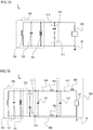
- FIG. 1A illustrates a simple circuit configuration (minimum circuit configuration) of the oscillator 1
- FIG. 1B illustrates a more detailed circuit configuration of the oscillator 1.
- the oscillator 1 includes an oscillation circuit 100, a voltage bias circuit 200, and a shunt element 310.
- the oscillation circuit 100 is a resonator (terahertz oscillation circuit) including elements such as a negative resistance element 101, a capacitor 102, and an inductor 103. More specifically, the negative resistance element 101, and the capacitor 102 and the inductor 103 which are connected in parallel to the negative resistance element 101 constitute the oscillation circuit 100.
- the oscillation circuit 100 causes the voltage bias circuit 200 to apply a predetermined voltage to the negative resistance element 101 to produce an oscillation of electromagnetic wave with a predetermined frequency of 30 GHz to 30 THz (a terahertz wave; a predetermined electromagnetic wave). That is, the predetermined electromagnetic wave is an electromagnetic wave that is mainly determined based on design parameters of the oscillation circuit 100 to cause the oscillation circuit 100 to oscillate (resonate). It is to be noted that the oscillation of the predetermined electromagnetic wave (terahertz wave) by the oscillation circuit 100 is hereinafter referred to as the "terahertz oscillation”.
- a voltage-controlled negative resistor may be used as the negative resistance element 101.
- a current-injection resonant tunnelling diode RTD
- This resonant tunnelling diode is composed of a GaAS and InP substrate and a quantum well made of GaAs/AlGaAs and InGaAs/InAlAs epitaxially grown in a lattice matching system on the GaAS and InP substrate.
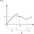
- FIG. 2 illustrates voltage-current characteristics of the negative resistance element (RTD) 101 when a voltage V is applied across both terminals (anode and cathode) of the negative resistance element 101 and accordingly, a current I flows through the negative resistance element 101.
- This voltage-current characteristic can be divided into two regions: a region PR in which the current value increases with increasing voltage and a region NR in which the current value decreases with increasing voltage.
- the region NR in which the current value decreases according to the increased voltage is a region having negative resistance characteristics, and is hereinafter referred to as the "negative resistance region".
- a voltage value Vop within the negative resistance region when a voltage value Vop within the negative resistance region is applied across both terminals of the negative resistance element 101, an electromagnetic wave (terahertz wave) oscillates with a terahertz frequency ft through the negative resistance element 101, the capacitor 102, and the inductor 103.
- the voltage value Vop to be applied is preferably set to a value of or around the center of the voltage range of the negative resistance region NR in order to enhance the stability of oscillation.
- the voltage is not limited to this, and any other voltage may be applied as long as it is within the negative resistance region.
- the current value flowing through the negative resistance element 101 when the voltage value Vop is applied is referred to as lop.
- a specific value of the voltage value Vop varies depending on the parameters of the negative resistance element 101, and is generally in a range of about 0.5 to 1.5 V (voltages) (at least 0.5 V and not more than 1.5 V) in many cases.
- a specific value of the current value lop varies depending on the parameters of the negative resistance element 101, and is generally in a range of about 20 to 150 mA (milliamperes) (at least 20 mA and not more than 150 mA) in many cases.
- the value ranges are not limited to such voltage value range and current value range, and any range out of such a range may be applied so that the same advantageous effect can be obtained.
- the voltage bias circuit 200 is a circuit for applying the voltage value Vop (DC voltage) in the negative resistance region to the negative resistance element (RTD) 101.
- the voltage bias circuit 200 includes, for example, an ideal voltage source 201, a parasitic inductor 411, a parasitic resistor 412, a parasitic capacitor 413, and the like as illustrated in FIG. 1B . Further, the voltage bias circuit 200 itself is not an ideal voltage source because it includes parasitic elements such as the parasitic inductor 411, the parasitic resistor 412, and the parasitic capacitor 413. Therefore, electromagnetic wave oscillation (parasitic oscillation) at a frequency other than the terahertz frequency ft may occur across the elements included in the oscillation circuit 100 and the parasitic elements included in the voltage bias circuit 200.
- a wiring section 400 is located between the oscillation circuit 100 and the voltage bias circuit 200 in many cases in order to implement various functions of the oscillator 1.
- the wiring section 400 is arranged between the oscillation circuit 100 and the voltage bias circuit 200, and includes, for example, four parasitic elements: a parasitic inductor 401, a parasitic inductor 402, a parasitic resistor 403, and a parasitic capacitor 404. Accordingly, parasitic oscillation may occur across the elements included in the oscillation circuit 100 and the parasitic elements included in the wiring section 400 at a frequency different from the terahertz frequency ft.
- the shunt element 310 prevents parasitic oscillation caused by the elements included in the oscillation circuit 100 described above and other parasitic elements.
- the shunt element 310 is composed of a resistive element 311 (shunt resistance element) and a capacitive element 312 (shunt capacitance element), which are arranged in series. It is to be noted that in the present embodiment, the "shunt element" has one terminal connected to a common wire (substrate; ground 20) and the other terminal connected to a wire between the oscillation circuit 100 and the voltage bias circuit 200.
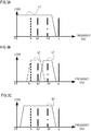
- FIGS. 3A and 3B illustrate loss characteristics (cut-off characteristics) of electromagnetic wave in a shunt element included in an oscillator of a comparative example.
- FIG. 3C illustrates loss characteristics of electromagnetic wave in the shunt element 310 of the oscillator 1 according to the present embodiment.
- FIGS. 3A to 3C are schematic diagrams illustrating the loss characteristics of the electromagnetic wave for each frequency in the shunt element.
- the horizontal axis indicates the frequency
- the vertical axis indicates an example of the magnitude of electromagnetic wave loss in the shunt element.
- the loss increases, it is possible to suppress the oscillation of the electromagnetic wave.
- the frequency at a boundary of the range where the shunt element has a loss is hereinafter referred to as the "cut-off frequency”.
- the shunt element can suppress the oscillation of electromagnetic waves in a frequency band between the cut-off frequency on the higher frequency side and the cut-off frequency on the lower frequency side.
- ft is a terahertz frequency (at least 30 GHz and not more than 30 THz)
- fp1, fp2, and fv are each a parasitic oscillation frequency.
- the parasitic oscillation frequencies fp1 and fp2 are oscillation frequencies of electromagnetic waves produced by the oscillation circuit 100 and the parasitic elements of the wiring section 400.
- the parasitic oscillation frequency fv is an oscillation frequency of an electromagnetic wave produced by the oscillation circuit 100 and the parasitic elements in the voltage bias circuit 200.
- FIG. 3A illustrates an example of loss characteristics in the case where a "resistive element (resistor)" is used as the shunt element.
- the shunt element has a loss L1 at all frequencies slightly lower than the terahertz frequency ft, and thus makes it possible to suppress the parasitic oscillation at the parasitic oscillation frequencies fp1, fp2, and fv. That is, in the present example, the oscillator has a loss in a wide frequency band, and thus makes it possible to sufficiently suppress the parasitic oscillation.
- the oscillator of the present example allows a current to flow through the resistive element constantly, which may cause unnecessary power consumption.
- FIG. 3B illustrates an example of loss characteristics in the case where "capacitive elements (capacitors)" are used as the shunt element.
- FIG. 3B also illustrates an example of a configuration of the oscillator including two capacitive elements. More specifically, the oscillator includes a capacitive element having a predetermined capacitance value (a capacitive element having a small capacitance value) and a capacitive element having a larger capacitance value.
- the capacitive element having a small capacitance value has a loss L3 around fp2, which is a frequency lower than the terahertz frequency ft, and suppresses the parasitic oscillation at the parasitic oscillation frequency fp2.
- the oscillator further includes the capacitive element having a large capacitance value.
- the capacitive element having a large capacitance value has a loss L2 around the parasitic oscillation frequencies fp1 and fv, which are lower than the parasitic oscillation frequency fp2, and suppresses the parasitic oscillation at the parasitic oscillation frequencies fp1 and fv.
- the parasitic oscillation frequency fv when the parasitic oscillation frequency fv is a low frequency, or when a parasitic oscillation frequency component lower than fv is included, it is difficult to generate a loss by the capacitive element in a low frequency range, making it difficult to suppress the parasitic oscillation. This is because it is easy to reduce the impedance of the capacitive element in a high frequency range, but it is difficult to reduce the impedance of the capacitive element in a low frequency range. Further, resonance may occur in the capacitive element used as the shunt element and the parasitic inductor 402 included in the wiring section 400, which even causes the capacitive element to generate parasitic oscillation.
- FIG. 3C illustrates an example of loss characteristics when an element in which the resistive element 311 (resistor) and the capacitive element 312 (capacitance) are connected in series is used as the shunt element 310, as in the present embodiment.
- the resistive element 311 has a loss L0.
- the resistive element 311 acts as a shunt element that suppresses the parasitic oscillation.
- unnecessary energy generated in the oscillation circuit 100 is appropriately lost by the resistive element 311.
- the parasitic elements of the wiring section 400 or the voltage bias circuit 200 and the oscillation circuit 100 from being coupled, and thus to suppress the parasitic oscillation.
- the impedance of the capacitive element 312 is large at not more than the cut-off frequency on the low frequency side of the shunt element 310. Accordingly, there is no loss generated by the shunt element 310 at the low frequency. In other words, the shunt element 310 is in an open state around the direct current and no loss is also generated by the resistive element 311, so that the power consumption of the entire oscillator 1 can be suppressed. Accordingly, the cut-off frequency on the low frequency side is set to be lower than the lowest parasitic oscillation frequency fv in the oscillation circuit 100, thereby making it possible to suppress the power consumption of the oscillator 1. It is to be noted that the cut-off frequency on the low frequency side is a frequency determined by the time constant of the capacitive element 312 and the resistive element 311, and can be adjusted to a very low frequency by adjusting their respective resistance value and capacitance value.
- the shunt element 310 includes the resistive element 311 (resistor) that suppresses the parasitic oscillation and the capacitive element 312 (capacitor) that suppresses the power consumption around a direct current. This makes it possible to suppress both the parasitic oscillation and unnecessary power.
- of the impedance of the negative resistance element 101 in the negative resistance region in order to stabilize the oscillation of terahertz waves.
- is preferably selected as the resistance value.
- the resistance value is 0.8 to 1.2 times (at least 0.8 and not more than 1.2 times) of
- of impedance in the negative resistance region of the resistive element 311 is typically in a range of several ohms to several tens of ohms. Further, depending on the oscillation frequency of the oscillator 1, the absolute value
- the capacitance value of the capacitive element 312 is preferably set to a value such that the cut-off frequency f0 on the low frequency side (frequency determined by the time constant of the resistive element 311 and the capacitive element 312) is not more than a lower limit frequency for suppressing the parasitic oscillation.
- the capacitance value C of the capacitive element 312 is set such that the impedance 1/(2 ⁇ f0 ⁇ C) of the capacitive element 312 at the frequency f0 is sufficiently lower than the resistance value R of the resistive element 311.
- the capacitance value C is set such that the impedance 1/(2 ⁇ f0 ⁇ C) preferably has at least the value of a fraction, more preferably at least the value of 1/10, of the resistance value R. In other words, it is desirable to satisfy R/10 ⁇ 1/(2 ⁇ f0 ⁇ C). For example, if the resistance value R is 10 ⁇ and the frequency f0 is 1 MHz, the capacitance value C of the capacitive element 312 is preferably at least 160 pF.
- the capacitance value C is as large as possible unless there is any problem with mounting size restrictions and the switching speed in an AC bias circuit used in a sixth embodiment described later.
- the values of the resistive element 311 and the capacitive element 312 are preferably set to optimum values based on the relationship between the parameters of the oscillation circuit and the parasitic oscillation frequency to be suppressed.
- the shunt element 310 it is necessary to carefully determine the position where the shunt element 310 is disposed. Specifically, it is necessary to set the length of a wire connecting the negative resistance element 101 and the shunt element 310 to not more than 1/4 of a wavelength ⁇ of an electromagnetic wave having the maximum parasitic oscillation frequency the parasitic oscillation of which is to be suppressed by the shunt element 310 (which has a loss). In the example illustrated in FIG. 3C , the length of the wire needs to be 1/4 of the wavelength of the electromagnetic wave having the parasitic oscillation frequency fp2. This is because, if the wavelength of an AC signal is short, its phase changes greatly only by slightly changing the position of the wire, and an equivalent capacitor or an equivalent inductor is generated due to reflection at the end of the wire.
- the shunt element 310 in order to suppress parasitic oscillation from gigahertz, which is a shorter wavelength, to terahertz, it is necessary to dispose the shunt element 310 closer to the negative resistance element 101. As described above, if the length of the wire connecting the negative resistance element 101 and the shunt element 310 is not more than 1/4 of the wavelength ⁇ , it is possible to prevent an equivalent capacitor or an equivalent inductor due to reflection at the end of the wire from being generated, and to suppress parasitic oscillation.
- the wavelength of the electromagnetic wave having the maximum parasitic oscillation frequency the parasitic oscillation of which is to be suppressed by the shunt element 310 may be referred to as a wavelength corresponding to the cut-off frequency on the high frequency side of the shunt element 310.
- the length of the wire connecting the negative resistance element 101 and the shunt element 310 may be set to not more than 1/4 of a wavelength ⁇ m of the predetermined electromagnetic wave (terahertz wave). This setting makes it possible to prevent an equivalent capacitor or an equivalent inductor due to reflection at the end of the wire from being generated at all the parasitic oscillation frequencies lower than the terahertz frequency ft of the predetermined electromagnetic wave, resulting in more effective suppression of the parasitic oscillation.
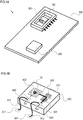
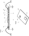
- FIG. 4A is a schematic diagram illustrating an external configuration of the oscillator 1 of the present embodiment
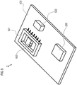
- FIG. 4B is a schematic diagram illustrating a chip 600 included in the oscillator 1 and its periphery in more detail.
- the oscillator 1 includes a printed circuit board (PCB) 500, a package (PKG) 501, a chip 600, and the voltage bias circuit 200, as illustrated in FIG. 4A .
- the chip 600 As illustrated in FIG. 4B , the chip 600, a wire 611, a wire 612, and electrodes 641 for wire bonding are formed on the chip 600 and its periphery.
- the chip 600 includes the oscillation circuit 100 including the negative resistance element 101, the shunt element 310, an antenna 602, a wire 603, a wire 605, and two electrodes 640 for wire bonding. Therefore, in the present embodiment, the oscillator 1 has a circuit configuration as illustrated in FIG. 7A , the oscillation circuit 100 and the shunt element 310 are formed on the chip 600, and the voltage bias circuit 200 is formed on the printed circuit board 500.
- the chip 600 is mounted in the package 501. As illustrated in FIG. 4B , the two electrodes 640 of the chip 600 are electrically connected to the two electrodes 641 included in the package 501 by wire bonding using the wires 611 and 612, respectively. It is to be noted that as the chip 600 is typically a slightly less than 1 mm square to several mm square chip when used, but may be as large as a 10 mm square chip.
- the package 501 and the voltage bias circuit 200 are mounted as illustrated in FIG. 4A . Accordingly, the oscillation circuit 100 and the voltage bias circuit 200 in the chip 600 are electrically connected via the wires of the printed circuit board 500 and the package 501. As a result, a DC voltage of voltage value Vop is applied from the voltage bias circuit 200 to the oscillation circuit 100, so that the oscillation circuit 100 is set to perform terahertz oscillation at the terahertz frequency ft.
- FIG. 5A is a diagram schematically illustrating an A1-A2-A3-A4 cross section of the chip 600 of FIG. 4B .
- an insulating film 620 is formed on the chip 600.
- the oscillation circuit 100 is formed on the chip 600 so as to be embedded in the depth direction of the insulating film 620, and one terminal of the oscillation circuit 100 is connected to the chip 600 (a substrate potential of the chip 600).
- the other terminal of the oscillation circuit 100 is connected to the antenna 602 formed on the chip 600.
- the substrate potential of the chip 600 is connected to the electrode 640 by a wire 613 penetrating the insulating film 620.
- the wire 603 is a wire for connecting the shunt element 310 and the oscillation circuit 100 (the negative resistance element 101).
- the size of the antenna 602 may be set to an optimum size according to the terahertz frequency ft.
- the size of the antenna 602 ranges from a hundred ⁇ m square to a few hundred ⁇ m square. It is to be noted that as the antenna 602, a larger antenna of several mm square can be used depending on the terahertz frequency ft.
- the antenna 602 of the oscillator 1 according to the present embodiment is not limited to a square antenna, and may have any antenna shape as long as it can output the predetermined electromagnetic wave (terahertz wave).
- FIG. 6A is an enlarged schematic diagram of the vicinity of the shunt element 310 illustrated in FIG. 4B .
- the shunt element 310 is connected to a contact point B0 between the wire 603 extending to the antenna 602 and the wire 605 extending to the electrode 640. As illustrated in FIG. 6A , a resistor part 631 of the resistive element 311 is connected to the contact point B0, and an upper electrode 632 of the capacitive element 312 is connected at the distal end of the resistor part 631.
- FIG. 6B is a schematic diagram of the shunt element 310 when cut along the B1-B2 cross section of FIG. 6A .
- a lower electrode 633 having the same size as the upper electrode 632 is formed on the chip 600, and a capacitor is formed by sequentially stacking the lower electrode 633, a dielectric film 634, and the upper electrode 632.
- the shunt element 310 includes, as the capacitive element 312, a MIM (Metal-Insulator-Metal) capacitor having a structure in which the dielectric film 634 (insulating film) is sandwiched between the metal lower electrode 633 and the metal upper electrode 632.
- MIM Metal-Insulator-Metal
- the shunt element 310 is electrically arranged in parallel to both terminals of the negative resistance element 101.
- the resistor part 631 can be easily formed by forming a pattern on a metal thin film so that it has a long wiring length.
- the configuration in which the configuration with the long wiring length is a meander wiring configuration in the example illustrated in FIG. 6A .
- the metal thin film any type of thin film can be used as long as it is a metal used for semiconductor wiring, such as aluminum. Further, the resistance value (sheet resistance value) of the metal thin film can be easily adjusted by adjusting the type of metal, the width, thickness, length, etc. of the wiring. It is to be noted that instead of the metal thin film, any resistor may be used as long as it can be formed into a desired resistor on the chip 600, including a polysilicon resistor whose resistance value is controlled by adjusting the doping amount to polysilicon.
- the dielectric film 634 can be easily formed using a silicon oxide film, a silicon nitride film, or the like. Specifically, the dielectric film 634 can be formed by selecting a low dielectric constant material or a high dielectric constant material in accordance with a desired dielectric constant.
- the upper electrode 632 and the lower electrode 633 can be easily formed from a metal material such as aluminum.
- a material that can withstand a temperature generated in a step of forming the dielectric film 634 it is necessary to select a material that can withstand a temperature generated in a step of forming the dielectric film 634.
- any type may be used as long as one having a desired capacitance value, including a capacitor using polysilicon as upper and lower electrodes and a MOS capacitor can be provided on the chip 600.
- a configuration not including the lower electrode 633 can be similarly used by substituting the chip 600 for the lower electrode 633.
- the insulating film 620 and the dielectric film 634 are formed of different materials, but are not limited to this.
- the same insulating film such as a silicon oxide film or a silicon nitride film may be used for the insulating film 620 and the dielectric film 634 as long as they have a desired capacitance value.
- Using the same insulating film does not require to form different insulating films (dielectric films) on the same chip 600, which makes it possible to form the chip 600 with a simpler structure and a simple manufacturing process.
- the oscillation circuit 100 and the shunt element 310 are formed on the chip 600 that is the same member, it is possible to shorten the length of the wire between the negative resistance element 101 and the shunt element 310 (length of the wire 603). In other words, it is possible to easily set the length of the wire 603 connecting the negative resistance element 101 and the shunt element 310 to be not more than the length of 1/4 of the wavelength ⁇ m of the predetermined electromagnetic wave. Accordingly, with such a small size configuration of the oscillator 1, it is possible to provide stable suppression of parasitic oscillation while preventing an increase in power consumption.
- the present invention is not limited to this configuration.
- a configuration in which the chip 600 is formed directly on the printed circuit board 500 without the package 501 may be used. This makes it possible to eliminate the package 501 in the oscillator 1, thereby configuring the oscillator 1 with fewer components.
- an oscillator that causes an oscillation circuit including a negative resistance element to oscillate at a predetermined frequency, it is possible to prevent an increase in power consumption and provide stable suppression of parasitic oscillation.
- An oscillator 2 according to a second embodiment is the same as the oscillator 1 according to the first embodiment except for the number of shunt elements and their arrangement place.
- the oscillator 2 according to the present embodiment will be described below with reference to FIG. 8 .
- two shunt elements are formed on different members (the chip and the printed circuit board).
- the oscillator 2 includes a shunt element 520 on the printed circuit board 500 in addition to the printed circuit board 500, the package 501, the chip 600, and the voltage bias circuit 200 included in the oscillator 1 according to the first embodiment.
- the chip 600 includes a capacitive element 302 as a shunt element in place of the shunt element 310 of the first embodiment.
- the capacitive element 302 is designed such that the length of the wire connecting the capacitive element 302 and the oscillation circuit 100 (negative resistance element 101) is within 1/4 of ⁇ m, to suppress parasitic oscillation with a high frequency not more than the terahertz frequency ft.
- the capacitive element 302 has a loss L4 around the parasitic oscillation frequency fp2 which is not more than the terahertz frequency ft.
- the length of the wire connecting the capacitive element 302 and the oscillation circuit 100 is not necessarily within ⁇ m/4. That length has only to be not more than 1/4 of the wavelength of an electromagnetic wave having the maximum parasitic oscillation frequency fp2 the oscillation of which is to be suppressed by the capacitive element 302 (which has a loss).
- the capacitive element 302 cannot sufficiently suppress parasitic oscillation at not more than a specific frequency (e.g., the parasitic oscillation frequency fp1).
- the shunt element 520 that suppresses the parasitic oscillation at not more than such a specific frequency is formed on the printed circuit board 500.
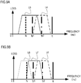
- the shunt element 520 has a loss L5 around the parasitic oscillation frequencies fp1 and fv as illustrated in FIG. 9A .
- the shunt element 520 is set such that the length of the wire connecting the shunt element 520 and the oscillation circuit 100 (negative resistance element 101) is within 1/4 of a wavelength ⁇ p1 of the parasitic oscillation frequency fp1. It is to be noted that the shunt element 520 includes the resistive element 311 and the capacitive element 312 in the same manner as the shunt element 310 described in the first embodiment, as illustrated in FIG. 7B , in order to obtain the effect of preventing an increase in power consumption. In addition, the resistive element 311 and the capacitive element 312 included in the shunt element 520 are preferably designed to satisfy the conditions on resistance value and capacitance value described in the first embodiment.
- the capacitive element 302 suppresses high-frequency parasitic oscillation, it is possible to dispose the shunt element 520 farther from the oscillation circuit 100. Therefore, even when a large component that is difficult to form on the chip 600 is used for the shunt element 520, the shunt element 520 can be disposed at an appropriate position.
- the shunt element 520 is preferably formed using a surface mount chip component such as a chip resistor or a chip capacitor. This is because the resistance value of the resistive element 311 and the capacitance value of the capacitive element 312 can be selected as any value.
- the chip resistor is formed by screen-printing a resistor such as a metal thin film on an alumina substrate, so that various resistance values and accuracy can be realized.
- the chip capacitor is formed by laminating several layers each having a structure in which a dielectric sheet is sandwiched between internal electrodes, and pressing and baking the laminate. Accordingly, the chip capacitor can have a small capacitance value (e.g., several pF) to a large capacitance value (e.g., several hundred ⁇ F) depending on the selection of the number of laminated layers and/or the dielectric sheet to be used.
- the present embodiment it is possible to easily select a large capacitance value for the shunt element 520, thereby providing more stable suppression of parasitic oscillation in a case where parasitic oscillation occurs at a lower frequency.
- the form in which the shunt element 520 is provided on a member different from the chip 600 on which the oscillation circuit 100 is formed has advantages of easy improvement of yield, easily change in the design of the shunt element 520, and easy customization.
- the capacitive element 302 is used as the shunt element formed in the chip 600.
- an element in which the capacitive element and the resistive element are electrically connected in series may be used as the shunt element.
- the shunt element 520 is formed on the printed circuit board 500.
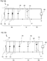
- the shunt element 520 is formed in the package 501 as illustrated in a circuit configuration diagram of FIG. 10A .
- the following description for the oscillator 3 according to the third embodiment will focus on different parts from the second embodiment with reference to FIGS. 11A and 11B .
- FIG. 11A is a schematic diagram illustrating the oscillator 3 of the present embodiment.
- the package 501 includes pins 503, and the printed circuit board 500 includes a pin socket 504 for the pins 503. Accordingly, the package 501 including the chip 600 can be inserted into and removed from the printed circuit board 500 as illustrated in FIG. 11B .
- the package 501 including the chip 600 can be inserted into and removed from the printed circuit board 500 as illustrated in FIG. 11B .
- the wire connecting the package 501 and the printed circuit board 500 includes a parasitic element, such as a parasitic inductor or a parasitic capacitor, caused by the pin socket 504.
- a parasitic element such as a parasitic inductor or a parasitic capacitor
- the terahertz wave oscillation can be stabilized even when a parasitic element is added outside the package 501.
- the loss of electromagnetic waves even at a sufficiently low frequency can occur in the package 501, making it possible to suppress the parasitic oscillation.
- the shunt element is not limited to the capacitive element 302. An element in which a capacitive element and a resistive element are electrically connected in series may be used as the shunt element in place of the capacitive element 302.
- the oscillator according to the present embodiment can be easily replaced, and can prevent an increase in power consumption and provide stable suppression of parasitic oscillation.
- a fourth embodiment is an embodiment in which the second embodiment and the third embodiment are combined. More specifically, in the present embodiment, three shunt elements are formed on different members (chip, package, printed circuit board). As illustrated in FIG. 12A , an oscillator 4 according to the present embodiment includes a capacitive element 502 having the same configuration as the capacitive element 302 on the printed circuit board 500 as in the second embodiment. Further, in the oscillator 4, the package 501 can be inserted into and removed from the printed circuit board 500 as in the third embodiment.
- the capacitive element 302 is formed as a shunt element.
- the capacitive element 502 is formed as a shunt element in the package 501.
- the shunt element 520 having the resistive element 311 and the capacitive element 312 is formed on the printed circuit board 500.
- the capacitive elements 302 and 502 and the shunt element 520 each have a parameter set so as to suppress different parasitic oscillations, and the frequency characteristics of loss are continuous as illustrated in FIG. 9B .
- the capacitive element 302 connected to the oscillation circuit 100 by a short wire has a loss L6 that suppresses the oscillation of the electromagnetic wave having the parasitic oscillation frequency fp2 which is a high-frequency.
- the capacitive element 502 connected to the oscillation circuit 100 by a wire having a long wire has a loss L7 that suppresses the oscillation of the electromagnetic wave having the parasitic oscillation frequency fp1.
- the shunt element 520 that requires a longer wire than the wire for the capacitive element 502 has a loss L8 that suppresses the oscillation of the electromagnetic wave having the parasitic oscillation frequency fv.
- the capacitive elements 302 and 502 and the shunt element 520 each suppress the oscillation of the electromagnetic wave in a higher frequency band as the wire for connection to the oscillation circuit 100 (negative resistance element 101) is shorter. Further, the capacitive elements 302 and 502 and the shunt element 520 are each connected to the oscillation circuit 100 (negative resistance element 101) by a wire having a length not more than 1/4 of the wavelength of an electromagnetic wave having the maximum frequency the parasitic oscillation of which is to be suppressed by the element itself (which has a loss). It is to be noted that as described above, the wavelength of an electromagnetic wave having the maximum frequency the parasitic oscillation of which is to be suppressed (which has a loss) may be referred to as a cut-off frequency on the high frequency side.
- the shunt element is not limited to the capacitive elements 302 and 502.
- An element in which a capacitive element and a resistive element are electrically connected in series may be used as the shunt element in place of the capacitive elements 302 and 502.
- the oscillator according to the present embodiment it is possible to suppress the parasitic oscillation for each portion to be connected (chip to package, package to printed circuit board, printed circuit board to voltage bias circuit) by using a plurality of shunt elements. Therefore, the parameter of each shunt element can be set to a more optimal parameter, which results in required minimum design values.
- An oscillator 5 according to a fifth embodiment is the same as the oscillator 1 according to the first embodiment except that the arrangement place of the voltage bias circuit is different from that of the oscillator 1 according to the first embodiment.
- the voltage bias circuit 200 is not formed on the printed circuit board 500 including the package 501, but is formed on another printed circuit board 510.
- the printed circuit board 500 and the printed circuit board 510 are electrically connected by a cable 513.
- a connector 511 on the printed circuit board 500 and a connector 512 on the printed circuit board 510 are connected by a cable 513.
- the voltage bias circuit 200 formed on the printed circuit board 510 can apply the voltage Vop to the chip 600 in the package 501 via the cable 513.
- the shunt element 310 makes it possible to suppress the parasitic oscillation. Accordingly, even if the voltage bias circuit 200 is separately disposed on the other printed circuit board 510, the oscillator 5 can produce the predetermined electromagnetic wave (terahertz wave) through the cable 513.
- a section where the predetermined electromagnetic wave is produced (a section having the oscillation circuit) and the voltage bias circuit can be separated, and thus it is possible to set the arrangement more feely with less restrictions on design for the section where the predetermined electromagnetic wave is produced.
- the voltage bias circuit applies a DC voltage across the negative resistance element.
- the voltage bias circuit applies an AC voltage across the negative resistance element. It is to be noted that the oscillator 6 has the same configuration as the oscillator 1 according to the first embodiment except for the application of an AC voltage.
- a voltage bias circuit 210 applies an alternating current voltage (AC voltage) to the oscillation circuit 100 (negative resistance element 101).
- AC voltage alternating current voltage
- a voltage changing with a certain frequency is used as the AC voltage, which is between a voltage value Vop for producing a predetermined electromagnetic wave and a voltage value Voff for stopping the production of the predetermined electromagnetic wave.
- the voltage value Voff has only to be a voltage value outside the negative resistance region, and is 0 V, for example.
- a voltage changing between two values: the voltage value Vop and the voltage value Voff by way of transition of pulse wave can be used as the AC voltage.
- the frequency with which the voltage changes a frequency that is sufficiently lower than the oscillation frequency of the predetermined electromagnetic wave is used.
- the voltage bias circuit 210 operates more complicatedly than the voltage bias circuit 200 according to the first embodiment because of generating an AC voltage. Therefore, the voltage bias circuit 210 includes a larger element than the parasitic element included in the voltage bias circuit 200 according to the first embodiment, in which parasitic oscillation due to the voltage bias circuit 210 and the oscillation circuit 100 is likely to occur. However, the oscillator 6 can effectively suppress the parasitic oscillation by including the shunt element 310 even in such a configuration in which the parasitic oscillation is more likely to occur.
- the frequency determined by the time constant of the capacitive element 312 and the resistive element 311 (the cut-off frequency on the low frequency side) needs to be higher than the frequency at which voltage bias circuit 210 changes voltage.
- the frequency determined by the time constant is preferably at least several times of the frequency at which voltage bias circuit 210 changes voltage.
- the voltage bias circuit 210 for alternating current in which parasitic oscillation is more likely to occur is used, it is possible to prevent an increase in power consumption and provide stable suppression of parasitic oscillation.
- the oscillator 1 according to the first embodiment is applicable to an imaging device (image acquisition device). Accordingly, an imaging device 10 using the oscillator 1 will be described in the present embodiment.
- the imaging device 10 includes an illumination 801 and an imaging element 802.
- the illumination 801 is an illumination device that includes the oscillator 1 according to the first embodiment to irradiate a subject 800 with a terahertz wave 811 (the predetermined electromagnetic wave).
- the image element 802 acquires (images) a terahertz wave 812 reflected from the subject 800.
- the image element 802 can acquire, as an image, information on the subject 800 that changes depending on the shape and/or physical property value of the subject 800.
- the oscillator 1 also when used for the illumination 801, makes it possible to prevent an increase in power consumption and provide stable suppression of parasitic oscillation in the imaging device 10. Accordingly, it is possible to perform stable irradiation with terahertz waves with little variation in properties due to heat generation or the like. Therefore, according to the present embodiment, it is possible to provide the imaging device 10 that can acquire accurate information on the subject 800.
- the illumination 801 is not limited to that used for the imaging device 10 according to the seventh embodiment, but may be used for an imaging device 11 including the oscillator 6 using the voltage bias circuit 210 of the sixth embodiment, as illustrated in FIG. 14B .
- the imaging device 11 includes the illumination 801 using the oscillator 6, the imaging element 802, and a timing generation unit 803.
- the timing generation unit 803 inputs a timing signal 810 to the illumination 801 using the oscillator 6 and to the imaging element 802.
- the illumination 801 adjusts the voltage change timing of the voltage bias circuit 210 based on the input timing signal 810.
- the illumination 801 when repeatedly producing and stopping the terahertz wave 811 at the adjusted timing in a cycle, causes a period in which the subject 800 is irradiated with the terahertz wave 811 and a period in which the subject 800 is not irradiated with the terahertz wave 811.
- the imaging element 802 performs imaging of the subject 800 in a period in which the illumination 801 emits the terahertz wave and a period in which the illumination 801 does not emit the terahertz wave, based on the input timing signal 810. Then, the imaging element 802 determines a difference between pieces of information imaged in the two periods. Based on the difference, the imaging element 802 can remove an electromagnetic wave component (noise component) that has not been intentionally emitted, thereby making it possible to improve the SN ratio (Signal to Noise Ratio) of the acquired image.
- an electromagnetic wave component noise component
- an imaging device (terahertz imaging device) that can acquire image information with a higher SN ratio.
- An oscillator (1) comprising: a resonator (100) including a negative resistance element (101); a voltage bias circuit (200, 210) configured to apply a voltage across the negative resistance element (101); and a first shunt element in which a resistor and a capacitor are electrically connected in series, wherein the negative resistance element (101) and the first shunt element are electrically connected in parallel to the voltage bias circuit (200, 210).
Landscapes
- Inductance-Capacitance Distribution Constants And Capacitance-Resistance Oscillators (AREA)
- Investigating Or Analysing Materials By Optical Means (AREA)
Abstract
Description
- The present technology relates to an oscillator and an imaging device.
- An oscillation circuit (resonator) including a negative resistance element such as a resonant tunnel diode (RTD) may be used as a small oscillator that generates a terahertz wave, which is a predetermined electromagnetic wave in a frequency band of 30 GHz to 30 THz. This oscillation circuit is connected to a voltage bias circuit that, for example, applies to the negative resistance element a voltage value to enable the negative resistance element to have negative resistance characteristics. It is to be noted that the negative resistance element has a gain in a wide frequency band as well as a predetermined electromagnetic wave frequency (predetermined frequency). For this reason, connecting the negative resistance element and the voltage bias circuit causes an oscillation of an electromagnetic wave at a resonance point lower than the predetermined frequency (hereinafter referred to as the "parasitic oscillation"), which should be suppressed.
- In this regard, Japanese Patent No.
5717336 5612842 oscillation circuit 100 with anegative resistance element 101 and also including avoltage bias circuit 200. As illustrated inFIG. 15A , Japanese Patent No.5717336 negative resistance element 101 to suppress parasitic oscillation. On the other hand, as illustrated inFIG. 15B , Japanese Patent No.5612842 negative resistance element 101 to suppress parasitic oscillation. - However, the oscillator according to Japanese Patent No.
5612842 resistive element 301, so thevoltage bias circuit 200 needs to constantly pass a direct current. This causes a problem that the oscillator needs to continue to consume power in order to stabilize the oscillation of a predetermined electromagnetic wave. On the other hand, the oscillator according to Japanese Patent No.5612842 voltage bias circuit 200. This makes it possible to reduce power consumption as compared with the oscillator according to Japanese Patent No.5612842 capacitive element 302. - Therefore, an oscillator provides stable suppression of parasitic oscillation while preventing an increase in power consumption.
- The present invention in its first aspect provides an oscillator as specified in claims 1to 16. The present invention in its second aspect provides an imaging device as specified in claim 17.
- According to the present technology, it is possible to provide stable suppression of parasitic oscillation in the oscillator while preventing an increase in power consumption.
- Further features of the present invention will become apparent from the following description of exemplary embodiments with reference to the attached drawings.
-
-
FIGS. 1A and 1B are each a circuit configuration diagram of an oscillator according to a first embodiment; -
FIG. 2 is a diagram for explaining voltage-current characteristics in a negative resistance element; -
FIGS. 3A and 3B each illustrate a loss of electromagnetic waves according to a comparative example; -
FIG. 3C illustrates a loss of electromagnetic waves according to the first embodiment; -
FIGS. 4A and 4B are diagrams each illustrating an external configuration of the oscillator according to the first embodiment; -
FIGS. 5A and 5B are diagrams each illustrating an external configuration of the oscillator according to the first embodiment; -
FIGS. 6A and 6B are diagrams each illustrating an external configuration of a shunt element according to the first embodiment; -
FIG. 7A is a circuit configuration diagram of the oscillator according to the first embodiment; -
FIG. 7B is a circuit configuration diagram of an oscillator according to a second embodiment; -
FIG. 8 is a diagram illustrating an external configuration of the oscillator according to the second embodiment; -
FIG. 9A illustrates a loss of electromagnetic waves according to the second embodiment; -
FIG. 9B illustrates a loss of electromagnetic waves according to a third embodiment; -
FIG. 10A is a circuit configuration diagram of an oscillator according to the third embodiment; -
FIG. 10B is a circuit configuration diagram of an oscillator according to a fourth embodiment; -
FIGS. 11A and 11B are diagrams each illustrating an external configuration of the oscillator according to the third embodiment; -
FIG. 12A is a diagram illustrating an external configuration of the oscillator according to the fourth embodiment; -
FIG. 12B is a diagram illustrating an external configuration of an oscillator according to a fifth embodiment; -
FIGS. 13A and 13B are for explaining the oscillator according to a fifth embodiment; -
FIG. 14A is a diagram illustrating an imaging device according to a sixth embodiment; -
FIG. 14B is a diagram illustrating an imaging device according to a first modification; and -
FIGS. 15A and 15B are circuit configuration diagrams each illustrating a conventional oscillator. - Hereinafter, embodiments of the disclosure of the present technology will be described with reference to the drawings. However, the disclosure of the present technology is not limited to the embodiments, and various modifications and changes are possible within the scope and spirit of the technology.
- An oscillator according to the present embodiment includes a voltage bias circuit that applies a voltage to a negative resistance element. The negative resistance element and a shunt element in which a resistor and a capacitor are arranged in series are electrically connected in parallel to the voltage bias circuit. This realizes an oscillator that is capable of providing stable suppression of parasitic oscillation while preventing an increase in power consumption.
- A circuit configuration of an
oscillator 1 according to the present embodiment will be described with reference toFIGS. 1A and 1B. FIG. 1A illustrates a simple circuit configuration (minimum circuit configuration) of theoscillator 1, andFIG. 1B illustrates a more detailed circuit configuration of theoscillator 1. Theoscillator 1 includes anoscillation circuit 100, avoltage bias circuit 200, and ashunt element 310. - The
oscillation circuit 100 is a resonator (terahertz oscillation circuit) including elements such as anegative resistance element 101, acapacitor 102, and aninductor 103. More specifically, thenegative resistance element 101, and thecapacitor 102 and theinductor 103 which are connected in parallel to thenegative resistance element 101 constitute theoscillation circuit 100. Theoscillation circuit 100 causes thevoltage bias circuit 200 to apply a predetermined voltage to thenegative resistance element 101 to produce an oscillation of electromagnetic wave with a predetermined frequency of 30 GHz to 30 THz (a terahertz wave; a predetermined electromagnetic wave). That is, the predetermined electromagnetic wave is an electromagnetic wave that is mainly determined based on design parameters of theoscillation circuit 100 to cause theoscillation circuit 100 to oscillate (resonate). It is to be noted that the oscillation of the predetermined electromagnetic wave (terahertz wave) by theoscillation circuit 100 is hereinafter referred to as the "terahertz oscillation". - As the
negative resistance element 101, a voltage-controlled negative resistor may be used. Specifically, using a current-injection resonant tunnelling diode (RTD) makes it possible to configure theoscillation circuit 100 with an electromagnetic wave of a predetermined frequency (terahertz frequency). This resonant tunnelling diode is composed of a GaAS and InP substrate and a quantum well made of GaAs/AlGaAs and InGaAs/InAlAs epitaxially grown in a lattice matching system on the GaAS and InP substrate. -
FIG. 2 illustrates voltage-current characteristics of the negative resistance element (RTD) 101 when a voltage V is applied across both terminals (anode and cathode) of thenegative resistance element 101 and accordingly, a current I flows through thenegative resistance element 101. This voltage-current characteristic can be divided into two regions: a region PR in which the current value increases with increasing voltage and a region NR in which the current value decreases with increasing voltage. The region NR in which the current value decreases according to the increased voltage is a region having negative resistance characteristics, and is hereinafter referred to as the "negative resistance region". Here, when a voltage value Vop within the negative resistance region is applied across both terminals of thenegative resistance element 101, an electromagnetic wave (terahertz wave) oscillates with a terahertz frequency ft through thenegative resistance element 101, thecapacitor 102, and theinductor 103. It is to be noted that the voltage value Vop to be applied is preferably set to a value of or around the center of the voltage range of the negative resistance region NR in order to enhance the stability of oscillation. However, the voltage is not limited to this, and any other voltage may be applied as long as it is within the negative resistance region. - The current value flowing through the
negative resistance element 101 when the voltage value Vop is applied is referred to as lop. It is to be noted that a specific value of the voltage value Vop varies depending on the parameters of thenegative resistance element 101, and is generally in a range of about 0.5 to 1.5 V (voltages) (at least 0.5 V and not more than 1.5 V) in many cases. On the other hand, a specific value of the current value lop varies depending on the parameters of thenegative resistance element 101, and is generally in a range of about 20 to 150 mA (milliamperes) (at least 20 mA and not more than 150 mA) in many cases. However, the value ranges are not limited to such voltage value range and current value range, and any range out of such a range may be applied so that the same advantageous effect can be obtained. - The
voltage bias circuit 200 is a circuit for applying the voltage value Vop (DC voltage) in the negative resistance region to the negative resistance element (RTD) 101. Thevoltage bias circuit 200 includes, for example, anideal voltage source 201, aparasitic inductor 411, aparasitic resistor 412, aparasitic capacitor 413, and the like as illustrated inFIG. 1B . Further, thevoltage bias circuit 200 itself is not an ideal voltage source because it includes parasitic elements such as theparasitic inductor 411, theparasitic resistor 412, and theparasitic capacitor 413. Therefore, electromagnetic wave oscillation (parasitic oscillation) at a frequency other than the terahertz frequency ft may occur across the elements included in theoscillation circuit 100 and the parasitic elements included in thevoltage bias circuit 200. - Although omitted in
FIG. 1A , as illustrated inFIG. 1B , awiring section 400 is located between theoscillation circuit 100 and thevoltage bias circuit 200 in many cases in order to implement various functions of theoscillator 1. - The
wiring section 400 is arranged between theoscillation circuit 100 and thevoltage bias circuit 200, and includes, for example, four parasitic elements: aparasitic inductor 401, aparasitic inductor 402, aparasitic resistor 403, and aparasitic capacitor 404. Accordingly, parasitic oscillation may occur across the elements included in theoscillation circuit 100 and the parasitic elements included in thewiring section 400 at a frequency different from the terahertz frequency ft. - The
shunt element 310 prevents parasitic oscillation caused by the elements included in theoscillation circuit 100 described above and other parasitic elements. Theshunt element 310 is composed of a resistive element 311 (shunt resistance element) and a capacitive element 312 (shunt capacitance element), which are arranged in series. It is to be noted that in the present embodiment, the "shunt element" has one terminal connected to a common wire (substrate; ground 20) and the other terminal connected to a wire between theoscillation circuit 100 and thevoltage bias circuit 200. - Next, the effect of the
shunt element 310 of the present embodiment suppressing the parasitic oscillation will be described with reference toFIGS. 3A to 3C. FIGS. 3A and 3B illustrate loss characteristics (cut-off characteristics) of electromagnetic wave in a shunt element included in an oscillator of a comparative example.FIG. 3C illustrates loss characteristics of electromagnetic wave in theshunt element 310 of theoscillator 1 according to the present embodiment. - Here,
FIGS. 3A to 3C are schematic diagrams illustrating the loss characteristics of the electromagnetic wave for each frequency in the shunt element. In the graphs illustrated inFIGS. 3A to 3C , the horizontal axis indicates the frequency, and the vertical axis indicates an example of the magnitude of electromagnetic wave loss in the shunt element. Here, as the loss (loss amount) increases, it is possible to suppress the oscillation of the electromagnetic wave. It is to be noted that the frequency at a boundary of the range where the shunt element has a loss is hereinafter referred to as the "cut-off frequency". Specifically, the shunt element can suppress the oscillation of electromagnetic waves in a frequency band between the cut-off frequency on the higher frequency side and the cut-off frequency on the lower frequency side. - In
FIGS. 3A to 3C , ft is a terahertz frequency (at least 30 GHz and not more than 30 THz), and fp1, fp2, and fv are each a parasitic oscillation frequency. The parasitic oscillation frequencies fp1 and fp2 are oscillation frequencies of electromagnetic waves produced by theoscillation circuit 100 and the parasitic elements of thewiring section 400. The parasitic oscillation frequency fv is an oscillation frequency of an electromagnetic wave produced by theoscillation circuit 100 and the parasitic elements in thevoltage bias circuit 200. - First,
FIG. 3A illustrates an example of loss characteristics in the case where a "resistive element (resistor)" is used as the shunt element. In this case, the shunt element has a loss L1 at all frequencies slightly lower than the terahertz frequency ft, and thus makes it possible to suppress the parasitic oscillation at the parasitic oscillation frequencies fp1, fp2, and fv. That is, in the present example, the oscillator has a loss in a wide frequency band, and thus makes it possible to sufficiently suppress the parasitic oscillation. On the other hand, the oscillator of the present example allows a current to flow through the resistive element constantly, which may cause unnecessary power consumption. -
FIG. 3B illustrates an example of loss characteristics in the case where "capacitive elements (capacitors)" are used as the shunt element.FIG. 3B also illustrates an example of a configuration of the oscillator including two capacitive elements. More specifically, the oscillator includes a capacitive element having a predetermined capacitance value (a capacitive element having a small capacitance value) and a capacitive element having a larger capacitance value. - The capacitive element having a small capacitance value has a loss L3 around fp2, which is a frequency lower than the terahertz frequency ft, and suppresses the parasitic oscillation at the parasitic oscillation frequency fp2. However, any loss at a lower frequency cannot be generated only by the capacitive element. For this reason, the oscillator further includes the capacitive element having a large capacitance value. The capacitive element having a large capacitance value has a loss L2 around the parasitic oscillation frequencies fp1 and fv, which are lower than the parasitic oscillation frequency fp2, and suppresses the parasitic oscillation at the parasitic oscillation frequencies fp1 and fv.
- However, in the present example, when the parasitic oscillation frequency fv is a low frequency, or when a parasitic oscillation frequency component lower than fv is included, it is difficult to generate a loss by the capacitive element in a low frequency range, making it difficult to suppress the parasitic oscillation. This is because it is easy to reduce the impedance of the capacitive element in a high frequency range, but it is difficult to reduce the impedance of the capacitive element in a low frequency range. Further, resonance may occur in the capacitive element used as the shunt element and the
parasitic inductor 402 included in thewiring section 400, which even causes the capacitive element to generate parasitic oscillation. -
FIG. 3C illustrates an example of loss characteristics when an element in which the resistive element 311 (resistor) and the capacitive element 312 (capacitance) are connected in series is used as theshunt element 310, as in the present embodiment. As illustrated inFIG. 3C , at a high frequency, theresistive element 311 has a loss L0. In other words, theresistive element 311 acts as a shunt element that suppresses the parasitic oscillation. In this manner, unnecessary energy generated in theoscillation circuit 100 is appropriately lost by theresistive element 311. Thereby making it possible to prevent the parasitic elements of thewiring section 400 or thevoltage bias circuit 200 and theoscillation circuit 100 from being coupled, and thus to suppress the parasitic oscillation. - On the other hand, the impedance of the
capacitive element 312 is large at not more than the cut-off frequency on the low frequency side of theshunt element 310. Accordingly, there is no loss generated by theshunt element 310 at the low frequency. In other words, theshunt element 310 is in an open state around the direct current and no loss is also generated by theresistive element 311, so that the power consumption of theentire oscillator 1 can be suppressed. Accordingly, the cut-off frequency on the low frequency side is set to be lower than the lowest parasitic oscillation frequency fv in theoscillation circuit 100, thereby making it possible to suppress the power consumption of theoscillator 1. It is to be noted that the cut-off frequency on the low frequency side is a frequency determined by the time constant of thecapacitive element 312 and theresistive element 311, and can be adjusted to a very low frequency by adjusting their respective resistance value and capacitance value. - It is to be noted that in the present embodiment, even if there is resonance between the
parasitic inductor 401 or theparasitic inductor 411 and thecapacitive element 312 in theshunt element 310, the loss of theresistive element 311 in theshunt element 310 makes it possible to suppress the parasitic oscillation. - As described above, the
shunt element 310 according to the present embodiment includes the resistive element 311 (resistor) that suppresses the parasitic oscillation and the capacitive element 312 (capacitor) that suppresses the power consumption around a direct current. This makes it possible to suppress both the parasitic oscillation and unnecessary power. - It is to be noted that it is preferable to select, for the
resistive element 311, a resistance value close to an absolute value |Zrtd| of the impedance of thenegative resistance element 101 in the negative resistance region, in order to stabilize the oscillation of terahertz waves. Specifically, a value of half to two times (at least 1/2 and not more than 2 times) of |Zrtd| is preferably selected as the resistance value. More preferably, the resistance value is 0.8 to 1.2 times (at least 0.8 and not more than 1.2 times) of |Zrtd|. - Selecting the resistance value in this way makes it possible to suppress the parasitic oscillation due to the parasitic elements more effectively and to stabilize the terahertz oscillation in the
oscillation circuit 100. It is to be noted that the absolute value |Zrtd| of impedance in the negative resistance region of theresistive element 311 is typically in a range of several ohms to several tens of ohms. Further, depending on the oscillation frequency of theoscillator 1, the absolute value |Zrtd| may be as large as about hundred ohms. - On the other hand, the capacitance value of the
capacitive element 312 is preferably set to a value such that the cut-off frequency f0 on the low frequency side (frequency determined by the time constant of theresistive element 311 and the capacitive element 312) is not more than a lower limit frequency for suppressing the parasitic oscillation. Specifically, the capacitance value C of thecapacitive element 312 is set such that theimpedance 1/(2πf0 × C) of thecapacitive element 312 at the frequency f0 is sufficiently lower than the resistance value R of theresistive element 311. The capacitance value C is set such that theimpedance 1/(2πf0 × C) preferably has at least the value of a fraction, more preferably at least the value of 1/10, of the resistance value R. In other words, it is desirable to satisfy R/10 ≥ 1/(2πf0 × C). For example, if the resistance value R is 10 Ω and the frequency f0 is 1 MHz, the capacitance value C of thecapacitive element 312 is preferably at least 160 pF. - It is to be noted that it is desirable that the capacitance value C is as large as possible unless there is any problem with mounting size restrictions and the switching speed in an AC bias circuit used in a sixth embodiment described later. The values of the
resistive element 311 and thecapacitive element 312 are preferably set to optimum values based on the relationship between the parameters of the oscillation circuit and the parasitic oscillation frequency to be suppressed. - In addition, it is necessary to carefully determine the position where the
shunt element 310 is disposed. Specifically, it is necessary to set the length of a wire connecting thenegative resistance element 101 and theshunt element 310 to not more than 1/4 of a wavelength λ of an electromagnetic wave having the maximum parasitic oscillation frequency the parasitic oscillation of which is to be suppressed by the shunt element 310 (which has a loss). In the example illustrated inFIG. 3C , the length of the wire needs to be 1/4 of the wavelength of the electromagnetic wave having the parasitic oscillation frequency fp2. This is because, if the wavelength of an AC signal is short, its phase changes greatly only by slightly changing the position of the wire, and an equivalent capacitor or an equivalent inductor is generated due to reflection at the end of the wire. In particular, in order to suppress parasitic oscillation from gigahertz, which is a shorter wavelength, to terahertz, it is necessary to dispose theshunt element 310 closer to thenegative resistance element 101. As described above, if the length of the wire connecting thenegative resistance element 101 and theshunt element 310 is not more than 1/4 of the wavelength λ, it is possible to prevent an equivalent capacitor or an equivalent inductor due to reflection at the end of the wire from being generated, and to suppress parasitic oscillation. It is to be noted that the wavelength of the electromagnetic wave having the maximum parasitic oscillation frequency the parasitic oscillation of which is to be suppressed by theshunt element 310 may be referred to as a wavelength corresponding to the cut-off frequency on the high frequency side of theshunt element 310. - It is to be noted that the length of the wire connecting the
negative resistance element 101 and theshunt element 310 may be set to not more than 1/4 of a wavelength λm of the predetermined electromagnetic wave (terahertz wave). This setting makes it possible to prevent an equivalent capacitor or an equivalent inductor due to reflection at the end of the wire from being generated at all the parasitic oscillation frequencies lower than the terahertz frequency ft of the predetermined electromagnetic wave, resulting in more effective suppression of the parasitic oscillation. - An external configuration of the
oscillator 1 will be described below with reference toFIGS. 4A to 6B .FIG. 4A is a schematic diagram illustrating an external configuration of theoscillator 1 of the present embodiment, andFIG. 4B is a schematic diagram illustrating achip 600 included in theoscillator 1 and its periphery in more detail. - The
oscillator 1 includes a printed circuit board (PCB) 500, a package (PKG) 501, achip 600, and thevoltage bias circuit 200, as illustrated inFIG. 4A . - As illustrated in
FIG. 4B , thechip 600, awire 611, awire 612, andelectrodes 641 for wire bonding are formed on thechip 600 and its periphery. Thechip 600 includes theoscillation circuit 100 including thenegative resistance element 101, theshunt element 310, anantenna 602, awire 603, awire 605, and twoelectrodes 640 for wire bonding. Therefore, in the present embodiment, theoscillator 1 has a circuit configuration as illustrated inFIG. 7A , theoscillation circuit 100 and theshunt element 310 are formed on thechip 600, and thevoltage bias circuit 200 is formed on the printedcircuit board 500. - The
chip 600 is mounted in thepackage 501. As illustrated inFIG. 4B , the twoelectrodes 640 of thechip 600 are electrically connected to the twoelectrodes 641 included in thepackage 501 by wire bonding using thewires chip 600 is typically a slightly less than 1 mm square to several mm square chip when used, but may be as large as a 10 mm square chip. - Further, on the printed
circuit board 500, thepackage 501 and thevoltage bias circuit 200 are mounted as illustrated inFIG. 4A . Accordingly, theoscillation circuit 100 and thevoltage bias circuit 200 in thechip 600 are electrically connected via the wires of the printedcircuit board 500 and thepackage 501. As a result, a DC voltage of voltage value Vop is applied from thevoltage bias circuit 200 to theoscillation circuit 100, so that theoscillation circuit 100 is set to perform terahertz oscillation at the terahertz frequency ft. -
FIG. 5A is a diagram schematically illustrating an A1-A2-A3-A4 cross section of thechip 600 ofFIG. 4B . As illustrated inFIG. 5A , an insulatingfilm 620 is formed on thechip 600. Theoscillation circuit 100 is formed on thechip 600 so as to be embedded in the depth direction of the insulatingfilm 620, and one terminal of theoscillation circuit 100 is connected to the chip 600 (a substrate potential of the chip 600). The other terminal of theoscillation circuit 100 is connected to theantenna 602 formed on thechip 600. It is to be noted that the substrate potential of thechip 600 is connected to theelectrode 640 by awire 613 penetrating the insulatingfilm 620. - One terminal of the
shunt element 310 is connected to the chip 600 (the substrate potential of the chip 600). The other terminal of theshunt element 310 is connected to theantenna 602 through thewire 603 and to theelectrode 640 through thewire 605. Accordingly, in the present embodiment, thewire 603 is a wire for connecting theshunt element 310 and the oscillation circuit 100 (the negative resistance element 101). - The size of the
antenna 602 may be set to an optimum size according to the terahertz frequency ft. For example, the size of theantenna 602 ranges from a hundred µm square to a few hundred µm square. It is to be noted that as theantenna 602, a larger antenna of several mm square can be used depending on the terahertz frequency ft. Further, theantenna 602 of theoscillator 1 according to the present embodiment is not limited to a square antenna, and may have any antenna shape as long as it can output the predetermined electromagnetic wave (terahertz wave). - A detailed configuration example of the
shunt element 310 will be described with reference toFIGS. 6A and 6B. FIG. 6A is an enlarged schematic diagram of the vicinity of theshunt element 310 illustrated inFIG. 4B . - The
shunt element 310 is connected to a contact point B0 between thewire 603 extending to theantenna 602 and thewire 605 extending to theelectrode 640. As illustrated inFIG. 6A , aresistor part 631 of theresistive element 311 is connected to the contact point B0, and anupper electrode 632 of thecapacitive element 312 is connected at the distal end of theresistor part 631. -
FIG. 6B is a schematic diagram of theshunt element 310 when cut along the B1-B2 cross section ofFIG. 6A . Alower electrode 633 having the same size as theupper electrode 632 is formed on thechip 600, and a capacitor is formed by sequentially stacking thelower electrode 633, adielectric film 634, and theupper electrode 632. Specifically, theshunt element 310 includes, as thecapacitive element 312, a MIM (Metal-Insulator-Metal) capacitor having a structure in which the dielectric film 634 (insulating film) is sandwiched between the metallower electrode 633 and the metalupper electrode 632. - Since the
lower electrode 633 is electrically connected to thechip 600, theshunt element 310 is electrically arranged in parallel to both terminals of thenegative resistance element 101. - The
resistor part 631 can be easily formed by forming a pattern on a metal thin film so that it has a long wiring length. The configuration in which the configuration with the long wiring length is a meander wiring configuration in the example illustrated inFIG. 6A . As the metal thin film, any type of thin film can be used as long as it is a metal used for semiconductor wiring, such as aluminum. Further, the resistance value (sheet resistance value) of the metal thin film can be easily adjusted by adjusting the type of metal, the width, thickness, length, etc. of the wiring. It is to be noted that instead of the metal thin film, any resistor may be used as long as it can be formed into a desired resistor on thechip 600, including a polysilicon resistor whose resistance value is controlled by adjusting the doping amount to polysilicon. - The
dielectric film 634 can be easily formed using a silicon oxide film, a silicon nitride film, or the like. Specifically, thedielectric film 634 can be formed by selecting a low dielectric constant material or a high dielectric constant material in accordance with a desired dielectric constant. - The
upper electrode 632 and thelower electrode 633 can be easily formed from a metal material such as aluminum. Here, for thelower electrode 633, it is necessary to select a material that can withstand a temperature generated in a step of forming thedielectric film 634. Further, as theupper electrode 632 and thelower electrode 633, any type may be used as long as one having a desired capacitance value, including a capacitor using polysilicon as upper and lower electrodes and a MOS capacitor can be provided on thechip 600. Further, if there is no problem in use, a configuration not including thelower electrode 633 can be similarly used by substituting thechip 600 for thelower electrode 633. - It is to be noted that in the present embodiment, the insulating
film 620 and thedielectric film 634 are formed of different materials, but are not limited to this. For example, the same insulating film such as a silicon oxide film or a silicon nitride film may be used for the insulatingfilm 620 and thedielectric film 634 as long as they have a desired capacitance value. Using the same insulating film does not require to form different insulating films (dielectric films) on thesame chip 600, which makes it possible to form thechip 600 with a simpler structure and a simple manufacturing process. - Further, in the present embodiment, since the
oscillation circuit 100 and theshunt element 310 are formed on thechip 600 that is the same member, it is possible to shorten the length of the wire between thenegative resistance element 101 and the shunt element 310 (length of the wire 603). In other words, it is possible to easily set the length of thewire 603 connecting thenegative resistance element 101 and theshunt element 310 to be not more than the length of 1/4 of the wavelength λm of the predetermined electromagnetic wave. Accordingly, with such a small size configuration of theoscillator 1, it is possible to provide stable suppression of parasitic oscillation while preventing an increase in power consumption. - It is to be noted that in the present embodiment, the configuration in which the
chip 600 is formed on thepackage 501 has been described, but the present invention is not limited to this configuration. For example, as illustrated inFIG. 5B , a configuration in which thechip 600 is formed directly on the printedcircuit board 500 without thepackage 501 may be used. This makes it possible to eliminate thepackage 501 in theoscillator 1, thereby configuring theoscillator 1 with fewer components. - According to the present embodiment, in an oscillator that causes an oscillation circuit including a negative resistance element to oscillate at a predetermined frequency, it is possible to prevent an increase in power consumption and provide stable suppression of parasitic oscillation.
- An oscillator 2 according to a second embodiment is the same as the
oscillator 1 according to the first embodiment except for the number of shunt elements and their arrangement place. The oscillator 2 according to the present embodiment will be described below with reference toFIG. 8 . In the oscillator 2 according to the present embodiment, two shunt elements are formed on different members (the chip and the printed circuit board). - The oscillator 2 includes a
shunt element 520 on the printedcircuit board 500 in addition to the printedcircuit board 500, thepackage 501, thechip 600, and thevoltage bias circuit 200 included in theoscillator 1 according to the first embodiment. - The
chip 600 includes acapacitive element 302 as a shunt element in place of theshunt element 310 of the first embodiment. Thecapacitive element 302 is designed such that the length of the wire connecting thecapacitive element 302 and the oscillation circuit 100 (negative resistance element 101) is within 1/4 of λm, to suppress parasitic oscillation with a high frequency not more than the terahertz frequency ft. Specifically, for example, as illustrated inFIG. 9A , thecapacitive element 302 has a loss L4 around the parasitic oscillation frequency fp2 which is not more than the terahertz frequency ft. It is to be noted that the length of the wire connecting thecapacitive element 302 and the oscillation circuit 100 (negative resistance element 101) is not necessarily within λm/4. That length has only to be not more than 1/4 of the wavelength of an electromagnetic wave having the maximum parasitic oscillation frequency fp2 the oscillation of which is to be suppressed by the capacitive element 302 (which has a loss). - On the other hand, the
capacitive element 302 cannot sufficiently suppress parasitic oscillation at not more than a specific frequency (e.g., the parasitic oscillation frequency fp1). For this reason, theshunt element 520 that suppresses the parasitic oscillation at not more than such a specific frequency is formed on the printedcircuit board 500. Specifically, for example, theshunt element 520 has a loss L5 around the parasitic oscillation frequencies fp1 and fv as illustrated inFIG. 9A . - Further, the
shunt element 520 is set such that the length of the wire connecting theshunt element 520 and the oscillation circuit 100 (negative resistance element 101) is within 1/4 of a wavelength λp1 of the parasitic oscillation frequency fp1. It is to be noted that theshunt element 520 includes theresistive element 311 and thecapacitive element 312 in the same manner as theshunt element 310 described in the first embodiment, as illustrated inFIG. 7B , in order to obtain the effect of preventing an increase in power consumption. In addition, theresistive element 311 and thecapacitive element 312 included in theshunt element 520 are preferably designed to satisfy the conditions on resistance value and capacitance value described in the first embodiment. - In this way, in the present embodiment, since the
capacitive element 302 suppresses high-frequency parasitic oscillation, it is possible to dispose theshunt element 520 farther from theoscillation circuit 100. Therefore, even when a large component that is difficult to form on thechip 600 is used for theshunt element 520, theshunt element 520 can be disposed at an appropriate position. - It is to be noted that the
shunt element 520 is preferably formed using a surface mount chip component such as a chip resistor or a chip capacitor. This is because the resistance value of theresistive element 311 and the capacitance value of thecapacitive element 312 can be selected as any value. - For example, the chip resistor is formed by screen-printing a resistor such as a metal thin film on an alumina substrate, so that various resistance values and accuracy can be realized. Further, the chip capacitor is formed by laminating several layers each having a structure in which a dielectric sheet is sandwiched between internal electrodes, and pressing and baking the laminate. Accordingly, the chip capacitor can have a small capacitance value (e.g., several pF) to a large capacitance value (e.g., several hundred µF) depending on the selection of the number of laminated layers and/or the dielectric sheet to be used.
- Therefore, in the present embodiment, it is possible to easily select a large capacitance value for the
shunt element 520, thereby providing more stable suppression of parasitic oscillation in a case where parasitic oscillation occurs at a lower frequency. In addition, the form in which theshunt element 520 is provided on a member different from thechip 600 on which theoscillation circuit 100 is formed, has advantages of easy improvement of yield, easily change in the design of theshunt element 520, and easy customization. - In the present embodiment, the
capacitive element 302 is used as the shunt element formed in thechip 600. However, an element in which the capacitive element and the resistive element are electrically connected in series may be used as the shunt element. - This enables the oscillator to provide stable suppression of parasitic oscillation in a wide frequency range from the terahertz frequency band to a sufficiently low frequency band. Furthermore, since chip components are used for the
shunt element 520, it is possible to more reliably suppress the parasitic oscillation with less design restriction. - In the oscillator 2 according to the second embodiment, the
shunt element 520 is formed on the printedcircuit board 500. However, in an oscillator 3 according to a third embodiment, theshunt element 520 is formed in thepackage 501 as illustrated in a circuit configuration diagram ofFIG. 10A . The following description for the oscillator 3 according to the third embodiment will focus on different parts from the second embodiment with reference toFIGS. 11A and 11B . -
FIG. 11A is a schematic diagram illustrating the oscillator 3 of the present embodiment. Thepackage 501 includespins 503, and the printedcircuit board 500 includes apin socket 504 for thepins 503. Accordingly, thepackage 501 including thechip 600 can be inserted into and removed from the printedcircuit board 500 as illustrated inFIG. 11B . Thus, in a case where a user desires to change the characteristics of the oscillator 3 or in a case where the oscillator 3 breaks down and needs to be replaced, it is possible to easily cope with such a case by replacing thepackage 501. - On the other hand, the wire connecting the
package 501 and the printedcircuit board 500 includes a parasitic element, such as a parasitic inductor or a parasitic capacitor, caused by thepin socket 504. For this reason, the oscillator 3 is more likely to generate parasitic oscillation and more easily interfere with terahertz wave oscillation than the oscillator 2 according to the second embodiment. - However, according to the configuration of the present embodiment, since the parasitic oscillation can be suppressed by the
shunt element 520 in thepackage 501, the terahertz wave oscillation can be stabilized even when a parasitic element is added outside thepackage 501. Specifically, according to the present embodiment, even when thepin socket 504 has a parasitic element, the loss of electromagnetic waves even at a sufficiently low frequency can occur in thepackage 501, making it possible to suppress the parasitic oscillation. - It is to be noted that a condition on length of the wire connecting the oscillation circuit 100 (negative resistance element 101) and the
shunt element 520 and a condition on length of the wire connecting the oscillation circuit 100 (negative resistance element 101) and thecapacitive element 302 are satisfied as in the second embodiment. Further, the shunt element is not limited to thecapacitive element 302. An element in which a capacitive element and a resistive element are electrically connected in series may be used as the shunt element in place of thecapacitive element 302. - Therefore, the oscillator according to the present embodiment can be easily replaced, and can prevent an increase in power consumption and provide stable suppression of parasitic oscillation.
- A fourth embodiment is an embodiment in which the second embodiment and the third embodiment are combined. More specifically, in the present embodiment, three shunt elements are formed on different members (chip, package, printed circuit board). As illustrated in
FIG. 12A , an oscillator 4 according to the present embodiment includes acapacitive element 502 having the same configuration as thecapacitive element 302 on the printedcircuit board 500 as in the second embodiment. Further, in the oscillator 4, thepackage 501 can be inserted into and removed from the printedcircuit board 500 as in the third embodiment. - In the
chip 600, as illustrated inFIG. 10B , thecapacitive element 302 is formed as a shunt element. On the other hand, thecapacitive element 502 is formed as a shunt element in thepackage 501. Further, theshunt element 520 having theresistive element 311 and thecapacitive element 312 is formed on the printedcircuit board 500. Thecapacitive elements shunt element 520 each have a parameter set so as to suppress different parasitic oscillations, and the frequency characteristics of loss are continuous as illustrated inFIG. 9B . - For example, in the present embodiment, as illustrated in
FIG. 9B , thecapacitive element 302 connected to theoscillation circuit 100 by a short wire has a loss L6 that suppresses the oscillation of the electromagnetic wave having the parasitic oscillation frequency fp2 which is a high-frequency. On the other hand, thecapacitive element 502 connected to theoscillation circuit 100 by a wire having a long wire has a loss L7 that suppresses the oscillation of the electromagnetic wave having the parasitic oscillation frequency fp1. In addition, theshunt element 520 that requires a longer wire than the wire for thecapacitive element 502 has a loss L8 that suppresses the oscillation of the electromagnetic wave having the parasitic oscillation frequency fv. - In other words, the
capacitive elements shunt element 520 each suppress the oscillation of the electromagnetic wave in a higher frequency band as the wire for connection to the oscillation circuit 100 (negative resistance element 101) is shorter. Further, thecapacitive elements shunt element 520 are each connected to the oscillation circuit 100 (negative resistance element 101) by a wire having a length not more than 1/4 of the wavelength of an electromagnetic wave having the maximum frequency the parasitic oscillation of which is to be suppressed by the element itself (which has a loss). It is to be noted that as described above, the wavelength of an electromagnetic wave having the maximum frequency the parasitic oscillation of which is to be suppressed (which has a loss) may be referred to as a cut-off frequency on the high frequency side. - It is to be noted that the shunt element is not limited to the
capacitive elements capacitive elements - With the oscillator according to the present embodiment, it is possible to suppress the parasitic oscillation for each portion to be connected (chip to package, package to printed circuit board, printed circuit board to voltage bias circuit) by using a plurality of shunt elements. Therefore, the parameter of each shunt element can be set to a more optimal parameter, which results in required minimum design values.
- An
oscillator 5 according to a fifth embodiment is the same as theoscillator 1 according to the first embodiment except that the arrangement place of the voltage bias circuit is different from that of theoscillator 1 according to the first embodiment. - In the present embodiment, as illustrated in
FIG. 12B , thevoltage bias circuit 200 is not formed on the printedcircuit board 500 including thepackage 501, but is formed on another printedcircuit board 510. Here, the printedcircuit board 500 and the printedcircuit board 510 are electrically connected by acable 513. Specifically, aconnector 511 on the printedcircuit board 500 and aconnector 512 on the printedcircuit board 510 are connected by acable 513. - Accordingly, the
voltage bias circuit 200 formed on the printedcircuit board 510 can apply the voltage Vop to thechip 600 in thepackage 501 via thecable 513. - In the present embodiment, even if there is a parasitic element between the
oscillation circuit 100 and thevoltage bias circuit 200, theshunt element 310 makes it possible to suppress the parasitic oscillation. Accordingly, even if thevoltage bias circuit 200 is separately disposed on the other printedcircuit board 510, theoscillator 5 can produce the predetermined electromagnetic wave (terahertz wave) through thecable 513. - Therefore, according to the present embodiment, in the oscillator, a section where the predetermined electromagnetic wave is produced (a section having the oscillation circuit) and the voltage bias circuit can be separated, and thus it is possible to set the arrangement more feely with less restrictions on design for the section where the predetermined electromagnetic wave is produced.
- In the
oscillator 1 according to the first embodiment, the voltage bias circuit applies a DC voltage across the negative resistance element. However, in an oscillator 6 according to the present embodiment, the voltage bias circuit applies an AC voltage across the negative resistance element. It is to be noted that the oscillator 6 has the same configuration as theoscillator 1 according to the first embodiment except for the application of an AC voltage. - As illustrated in
FIG. 13A , avoltage bias circuit 210 applies an alternating current voltage (AC voltage) to the oscillation circuit 100 (negative resistance element 101). Specifically, as illustrated inFIG. 13B , a voltage changing with a certain frequency is used as the AC voltage, which is between a voltage value Vop for producing a predetermined electromagnetic wave and a voltage value Voff for stopping the production of the predetermined electromagnetic wave. The voltage value Voff has only to be a voltage value outside the negative resistance region, and is 0 V, for example. Further, as illustrated inFIG. 13B , a voltage changing between two values: the voltage value Vop and the voltage value Voff by way of transition of pulse wave can be used as the AC voltage. As the frequency with which the voltage changes, a frequency that is sufficiently lower than the oscillation frequency of the predetermined electromagnetic wave is used. - The
voltage bias circuit 210 operates more complicatedly than thevoltage bias circuit 200 according to the first embodiment because of generating an AC voltage. Therefore, thevoltage bias circuit 210 includes a larger element than the parasitic element included in thevoltage bias circuit 200 according to the first embodiment, in which parasitic oscillation due to thevoltage bias circuit 210 and theoscillation circuit 100 is likely to occur. However, the oscillator 6 can effectively suppress the parasitic oscillation by including theshunt element 310 even in such a configuration in which the parasitic oscillation is more likely to occur. - It is to be noted that in the
shunt element 310, the frequency determined by the time constant of thecapacitive element 312 and the resistive element 311 (the cut-off frequency on the low frequency side) needs to be higher than the frequency at whichvoltage bias circuit 210 changes voltage. For example, in a case where a rectangular wave voltage is used, the frequency determined by the time constant is preferably at least several times of the frequency at whichvoltage bias circuit 210 changes voltage. - According to the present embodiment, even in a case where the
voltage bias circuit 210 for alternating current in which parasitic oscillation is more likely to occur is used, it is possible to prevent an increase in power consumption and provide stable suppression of parasitic oscillation. - The
oscillator 1 according to the first embodiment is applicable to an imaging device (image acquisition device). Accordingly, animaging device 10 using theoscillator 1 will be described in the present embodiment. - As illustrated in
FIG. 14A , theimaging device 10 includes anillumination 801 and animaging element 802. Theillumination 801 is an illumination device that includes theoscillator 1 according to the first embodiment to irradiate a subject 800 with a terahertz wave 811 (the predetermined electromagnetic wave). Theimage element 802 acquires (images) aterahertz wave 812 reflected from the subject 800. Theimage element 802 can acquire, as an image, information on the subject 800 that changes depending on the shape and/or physical property value of the subject 800. - In this way, the
oscillator 1, also when used for theillumination 801, makes it possible to prevent an increase in power consumption and provide stable suppression of parasitic oscillation in theimaging device 10. Accordingly, it is possible to perform stable irradiation with terahertz waves with little variation in properties due to heat generation or the like. Therefore, according to the present embodiment, it is possible to provide theimaging device 10 that can acquire accurate information on the subject 800. - Furthermore, the
illumination 801 is not limited to that used for theimaging device 10 according to the seventh embodiment, but may be used for animaging device 11 including the oscillator 6 using thevoltage bias circuit 210 of the sixth embodiment, as illustrated inFIG. 14B . - In
FIG. 14B , theimaging device 11 includes theillumination 801 using the oscillator 6, theimaging element 802, and atiming generation unit 803. Thetiming generation unit 803 inputs atiming signal 810 to theillumination 801 using the oscillator 6 and to theimaging element 802. - The
illumination 801 adjusts the voltage change timing of thevoltage bias circuit 210 based on theinput timing signal 810. Theillumination 801, when repeatedly producing and stopping theterahertz wave 811 at the adjusted timing in a cycle, causes a period in which the subject 800 is irradiated with theterahertz wave 811 and a period in which the subject 800 is not irradiated with theterahertz wave 811. - On the other hand, the
imaging element 802 performs imaging of the subject 800 in a period in which theillumination 801 emits the terahertz wave and a period in which theillumination 801 does not emit the terahertz wave, based on theinput timing signal 810. Then, theimaging element 802 determines a difference between pieces of information imaged in the two periods. Based on the difference, theimaging element 802 can remove an electromagnetic wave component (noise component) that has not been intentionally emitted, thereby making it possible to improve the SN ratio (Signal to Noise Ratio) of the acquired image. - According to the present modification, it is possible to provide an imaging device (terahertz imaging device) that can acquire image information with a higher SN ratio.
- While the present invention has been described with reference to exemplary embodiments, it is to be understood that the invention is not limited to the disclosed exemplary embodiments. The scope of the following claims is to be accorded the broadest interpretation so as to encompass all such modifications and equivalent structures and functions.
- An oscillator (1) comprising: a resonator (100) including a negative resistance element (101); a voltage bias circuit (200, 210) configured to apply a voltage across the negative resistance element (101); and a first shunt element in which a resistor and a capacitor are electrically connected in series, wherein the negative resistance element (101) and the first shunt element are electrically connected in parallel to the voltage bias circuit (200, 210).
Claims (17)
- An oscillator (1) comprising:a resonator (100) including a negative resistance element (101);a voltage bias circuit (200, 210) configured to apply a voltage across the negative resistance element (101); anda first shunt element in which a resistor and a capacitor are electrically connected in series, whereinthe negative resistance element (101) and the first shunt element are electrically connected in parallel to the voltage bias circuit (200, 210).
- The oscillator (1) according to claim 1, wherein a wire connecting the negative resistance element (101) and the first shunt element has a length of not more than 1/4 of a wavelength of an electromagnetic wave produced by the resonator (100).
- The oscillator (1) according to claim 1 or 2, wherein the resonator (100) and the first shunt element are formed on a same chip.
- The oscillator (1) according to claim 1 or 2, further comprising one or a plurality of second shunt elements, wherein
each of the one or a plurality of second shunt elements includes a capacitor, and
each of the one or a plurality of second shunt elements, the negative resistance element (101), and the first shunt element are electrically connected in parallel to the voltage bias circuit (200, 210). - The oscillator (1) according to claim 4, wherein a wire connecting at least one of the one or a plurality of second shunt elements and the negative resistance element (101) has a length of not more than 1/4 of a wavelength of an electromagnetic wave produced by the resonator (100).
- The oscillator (1) according to claim 4 or 5, wherein the first shunt element and the one or a plurality of second shunt elements are each connected to the negative resistance element (101) by a wire having a length of not more than 1/4 of a wavelength corresponding to a cut-off frequency on a high frequency side.
- The oscillator (1) according to any one of claims 4 to 6, wherein the first shunt element and the one or a plurality of second shunt elements each suppress oscillation of an electromagnetic wave in a higher frequency band as a wire for connection to the negative resistance element (101) is shorter.
- The oscillator (1) according to any one of claims 4 to 7, wherein the resonator (100) and one of the one or a plurality of second shunt elements are formed on a same chip.
- The oscillator (1) according to any one of claims 4 to 8, wherein the first shunt element and the one or a plurality of second shunt elements are each formed on a different member.
- The oscillator (1) according to any one of claims 4 to 9, wherein each of the one or a plurality of second shunt elements does not include a resistor.
- The oscillator (1) according to any one of claims 1 to 10, further comprising:a first substrate (510) on which the voltage bias circuit (200, 210) is formed; anda second substrate (500) on which the resonator (100) is formed, whereinthe first substrate (510) and the second substrate (510) are electrically connected via a cable (513).
- The oscillator (1) according to any one of claims 1 to 11, wherein
the resistor of the first shunt element has a resistance value of at least 1/2 and not more than two times of an absolute value of an impedance of the negative resistance element (101) in a negative resistance region, and
the negative resistance region is a region where a current decreases as a voltage increases in voltage-current characteristics. - The oscillator (1) according to any one of claims 1 to 12, wherein R/10 ≥ 1/(2πf0 × C) is satisfied, where C is a capacitance value of the capacitor of the first shunt element, R is a resistance value of the resistor of the first shunt element, and f0 is a cut-off frequency on a low frequency side of the first shunt element.
- The oscillator (1) according to any one of claims 1 to 13, wherein the voltage bias circuit (200, 210) applies an alternating voltage across the negative resistance element (101).
- The oscillator (1) according to any one of claims 1 to 14, wherein a frequency of an electromagnetic wave produced by the resonator (100) is at least 30 GHz and not more than 30 THz.
- The oscillator (1) according to any one of claims 1 to 15, wherein the first shunt element includes a capacitor in which a dielectric film is sandwiched between two electrodes.
- Am imaging device (10) comprising:an illumination device (801) including the oscillator (1) according to any one of claims 1 to 16; andan imaging element (802) configured to image a subject irradiated with an electromagnetic wave produced by the oscillator (1).
Applications Claiming Priority (1)
| Application Number | Priority Date | Filing Date | Title |
|---|---|---|---|
| JP2019028242A JP7516009B2 (en) | 2019-02-20 | 2019-02-20 | Oscillators, imaging devices |
Publications (1)
| Publication Number | Publication Date |
|---|---|
| EP3700085A1 true EP3700085A1 (en) | 2020-08-26 |
Family
ID=69701103
Family Applications (1)
| Application Number | Title | Priority Date | Filing Date |
|---|---|---|---|
| EP20158189.9A Pending EP3700085A1 (en) | 2019-02-20 | 2020-02-19 | Oscillator and imaging device |
Country Status (4)
| Country | Link |
|---|---|
| US (1) | US11025199B2 (en) |
| EP (1) | EP3700085A1 (en) |
| JP (1) | JP7516009B2 (en) |
| CN (1) | CN111600549B (en) |
Families Citing this family (6)
| Publication number | Priority date | Publication date | Assignee | Title |
|---|---|---|---|---|
| JP7414428B2 (en) | 2019-08-26 | 2024-01-16 | キヤノン株式会社 | Oscillators, illumination devices, imaging devices and equipment |
| JP7493922B2 (en) | 2019-08-26 | 2024-06-03 | キヤノン株式会社 | Oscillators, imaging devices |
| WO2022168479A1 (en) * | 2021-02-03 | 2022-08-11 | キヤノン株式会社 | Antenna device and camera system |
| JP7746142B2 (en) * | 2021-02-03 | 2025-09-30 | キヤノン株式会社 | Antenna device and camera system |
| JP7844156B2 (en) * | 2021-12-23 | 2026-04-13 | キヤノン株式会社 | High-frequency circuit device and detection system |
| WO2026079195A1 (en) * | 2024-10-07 | 2026-04-16 | ローム株式会社 | Terahertz device |
Citations (5)
| Publication number | Priority date | Publication date | Assignee | Title |
|---|---|---|---|---|
| JPS5612842B2 (en) | 1973-07-06 | 1981-03-25 | ||
| JPS5717336B2 (en) | 1974-05-11 | 1982-04-10 | ||
| US20120119838A1 (en) * | 2009-09-07 | 2012-05-17 | Canon Kabushiki Kaisha | Oscillation circuit having negative resistance element and oscillator using the oscillation circuit |
| US20130328635A1 (en) * | 2012-06-06 | 2013-12-12 | Canon Kabushiki Kaisha | Oscillator |
| US20170155361A1 (en) * | 2014-05-08 | 2017-06-01 | Tokyo Institute Of Technology | Frequency-variable terahertz oscillator and method for manufacturing the same |
Family Cites Families (34)
| Publication number | Priority date | Publication date | Assignee | Title |
|---|---|---|---|---|
| US4518930A (en) * | 1982-07-30 | 1985-05-21 | Rockwell International Corporation | Negative resistance circuit for VCO |
| JP3461236B2 (en) | 1996-01-19 | 2003-10-27 | キヤノン株式会社 | Radiation imaging apparatus and image processing method and apparatus |
| JP4164134B2 (en) | 1997-05-26 | 2008-10-08 | キヤノン株式会社 | Imaging apparatus and imaging method |
| JP2001074847A (en) | 1999-07-08 | 2001-03-23 | Canon Inc | Radiation imaging apparatus and radiation imaging system |
| JP3631114B2 (en) | 2000-08-01 | 2005-03-23 | キヤノン株式会社 | Imaging device |
| JP3548507B2 (en) | 2000-08-01 | 2004-07-28 | キヤノン株式会社 | Radiation imaging device |
| JP2003017676A (en) | 2001-04-27 | 2003-01-17 | Canon Inc | Radiation imaging apparatus and radiation imaging system using the same |
| JP3950665B2 (en) | 2001-10-23 | 2007-08-01 | キヤノン株式会社 | Radiation imaging apparatus and imaging method of radiation imaging apparatus |
| JP2006003131A (en) | 2004-06-15 | 2006-01-05 | Canon Inc | Potential sensor |
| US7382137B2 (en) | 2005-05-27 | 2008-06-03 | Canon Kabushiki Kaisha | Potential measuring apparatus |
| JP5159062B2 (en) | 2006-08-09 | 2013-03-06 | キヤノン株式会社 | Angular velocity sensor |
| JP5105949B2 (en) | 2007-04-27 | 2012-12-26 | キヤノン株式会社 | Sensor |
| JP5432440B2 (en) | 2007-07-04 | 2014-03-05 | キヤノン株式会社 | Oscillator device |
| JP5247182B2 (en) | 2008-02-19 | 2013-07-24 | キヤノン株式会社 | Angular velocity sensor |
| JP5473253B2 (en) | 2008-06-02 | 2014-04-16 | キヤノン株式会社 | Structure having a plurality of conductive regions and manufacturing method thereof |
| JP5717336B2 (en) | 2009-03-27 | 2015-05-13 | キヤノン株式会社 | Oscillator |
| JP5578810B2 (en) * | 2009-06-19 | 2014-08-27 | キヤノン株式会社 | Capacitance type electromechanical transducer |
| JP5612842B2 (en) | 2009-09-07 | 2014-10-22 | キヤノン株式会社 | Oscillator |
| JP5473579B2 (en) | 2009-12-11 | 2014-04-16 | キヤノン株式会社 | Control device for capacitive electromechanical transducer and control method for capacitive electromechanical transducer |
| JP5424847B2 (en) | 2009-12-11 | 2014-02-26 | キヤノン株式会社 | Electromechanical converter |
| JP5414546B2 (en) | 2010-01-12 | 2014-02-12 | キヤノン株式会社 | Capacitance detection type electromechanical transducer |
| JP5603739B2 (en) | 2010-11-02 | 2014-10-08 | キヤノン株式会社 | Capacitance type electromechanical transducer |
| US9608567B2 (en) | 2011-05-30 | 2017-03-28 | Acconeer Ab | Transceiver module |
| JP5947511B2 (en) | 2011-09-08 | 2016-07-06 | キヤノン株式会社 | Electromechanical converter |
| JP5893352B2 (en) | 2011-11-14 | 2016-03-23 | キヤノン株式会社 | Electromechanical converter |
| JP6296681B2 (en) | 2012-01-19 | 2018-03-20 | キヤノン株式会社 | Oscillation element, oscillator, and imaging apparatus using the same |
| US8593180B2 (en) | 2012-03-12 | 2013-11-26 | International Business Machines Corporation | Circuit including a negative differential resistance (NDR) device having a graphene channel, and method of operating the circuit |
| JP6234073B2 (en) | 2013-06-07 | 2017-11-22 | キヤノン株式会社 | Capacitance transducer driving apparatus and subject information acquiring apparatus |
| JP2015144248A (en) * | 2013-12-25 | 2015-08-06 | キヤノン株式会社 | Semiconductor device, and method for manufacturing the same |
| JP6562645B2 (en) * | 2014-02-28 | 2019-08-21 | キヤノン株式会社 | Oscillating element and oscillator using the same |
| JP6446250B2 (en) | 2014-12-08 | 2018-12-26 | ローム株式会社 | Resonant tunnel diode type oscillator and manufacturing method thereof |
| JP6472313B2 (en) | 2015-04-16 | 2019-02-20 | キヤノン株式会社 | Probe and information acquisition device |
| JP6904760B2 (en) | 2016-04-28 | 2021-07-21 | キヤノン株式会社 | element |
| CN208285281U (en) * | 2018-06-27 | 2018-12-25 | 深圳市太赫兹科技创新研究院 | A kind of Terahertz oscillating circuit and oscillator based on resonant-tunneling diode |
-
2019
- 2019-02-20 JP JP2019028242A patent/JP7516009B2/en active Active
-
2020
- 2020-02-17 CN CN202010094818.XA patent/CN111600549B/en active Active
- 2020-02-19 EP EP20158189.9A patent/EP3700085A1/en active Pending
- 2020-02-20 US US16/795,987 patent/US11025199B2/en active Active
Patent Citations (5)
| Publication number | Priority date | Publication date | Assignee | Title |
|---|---|---|---|---|
| JPS5612842B2 (en) | 1973-07-06 | 1981-03-25 | ||
| JPS5717336B2 (en) | 1974-05-11 | 1982-04-10 | ||
| US20120119838A1 (en) * | 2009-09-07 | 2012-05-17 | Canon Kabushiki Kaisha | Oscillation circuit having negative resistance element and oscillator using the oscillation circuit |
| US20130328635A1 (en) * | 2012-06-06 | 2013-12-12 | Canon Kabushiki Kaisha | Oscillator |
| US20170155361A1 (en) * | 2014-05-08 | 2017-06-01 | Tokyo Institute Of Technology | Frequency-variable terahertz oscillator and method for manufacturing the same |
Also Published As
| Publication number | Publication date |
|---|---|
| JP2020136910A (en) | 2020-08-31 |
| CN111600549B (en) | 2025-01-07 |
| US11025199B2 (en) | 2021-06-01 |
| JP7516009B2 (en) | 2024-07-16 |
| US20200266762A1 (en) | 2020-08-20 |
| CN111600549A (en) | 2020-08-28 |
Similar Documents
| Publication | Publication Date | Title |
|---|---|---|
| US11025199B2 (en) | Oscillator and imaging device | |
| US11770102B2 (en) | Oscillator and imaging device | |
| US8410860B2 (en) | Oscillator with resonator generating terahertz wave | |
| JP6280310B2 (en) | Oscillator | |
| US8816785B2 (en) | Oscillator | |
| TWI894498B (en) | High-frequency circuit device and detection system | |
| CN112635960A (en) | Device and method for manufacturing device | |
| US11283406B2 (en) | Oscillator, illumination device, and imaging device | |
| CN1695293B (en) | Integrated circuit oscillator | |
| CN116472647A (en) | Component, and a terahertz camera system using the component | |
| JP6870135B2 (en) | element | |
| JP2022070824A (en) | Element, and terahertz camera system using element | |
| HK1077130B (en) | Integrated circuit oscillator |
Legal Events
| Date | Code | Title | Description |
|---|---|---|---|
| PUAI | Public reference made under article 153(3) epc to a published international application that has entered the european phase |
Free format text: ORIGINAL CODE: 0009012 |
|
| STAA | Information on the status of an ep patent application or granted ep patent |
Free format text: STATUS: THE APPLICATION HAS BEEN PUBLISHED |
|
| AK | Designated contracting states |
Kind code of ref document: A1 Designated state(s): AL AT BE BG CH CY CZ DE DK EE ES FI FR GB GR HR HU IE IS IT LI LT LU LV MC MK MT NL NO PL PT RO RS SE SI SK SM TR |
|
| AX | Request for extension of the european patent |
Extension state: BA ME |
|
| STAA | Information on the status of an ep patent application or granted ep patent |
Free format text: STATUS: REQUEST FOR EXAMINATION WAS MADE |
|
| 17P | Request for examination filed |
Effective date: 20210226 |
|
| RBV | Designated contracting states (corrected) |
Designated state(s): AL AT BE BG CH CY CZ DE DK EE ES FI FR GB GR HR HU IE IS IT LI LT LU LV MC MK MT NL NO PL PT RO RS SE SI SK SM TR |
|
| STAA | Information on the status of an ep patent application or granted ep patent |
Free format text: STATUS: EXAMINATION IS IN PROGRESS |
|
| 17Q | First examination report despatched |
Effective date: 20210922 |