EP3699978B1 - Power supply device and method for providing the power supply device - Google Patents
Power supply device and method for providing the power supply device Download PDFInfo
- Publication number
- EP3699978B1 EP3699978B1 EP20157856.4A EP20157856A EP3699978B1 EP 3699978 B1 EP3699978 B1 EP 3699978B1 EP 20157856 A EP20157856 A EP 20157856A EP 3699978 B1 EP3699978 B1 EP 3699978B1
- Authority
- EP
- European Patent Office
- Prior art keywords
- power supply
- controller
- supply module
- module
- tray
- Prior art date
- Legal status (The legal status is an assumption and is not a legal conclusion. Google has not performed a legal analysis and makes no representation as to the accuracy of the status listed.)
- Active
Links
Images




Classifications
-
- H—ELECTRICITY
- H02—GENERATION; CONVERSION OR DISTRIBUTION OF ELECTRIC POWER
- H02J—ELECTRIC POWER NETWORKS; CIRCUIT ARRANGEMENTS OR SYSTEMS FOR SUPPLYING OR DISTRIBUTING ELECTRIC POWER; SYSTEMS FOR STORING ELECTRIC ENERGY
- H02J7/00—Circuit arrangements for charging or discharging batteries or for supplying loads from batteries
- H02J7/70—Circuit arrangements for charging or discharging batteries or for supplying loads from batteries characterised by the mechanical construction
-
- H—ELECTRICITY
- H02—GENERATION; CONVERSION OR DISTRIBUTION OF ELECTRIC POWER
- H02J—ELECTRIC POWER NETWORKS; CIRCUIT ARRANGEMENTS OR SYSTEMS FOR SUPPLYING OR DISTRIBUTING ELECTRIC POWER; SYSTEMS FOR STORING ELECTRIC ENERGY
- H02J9/00—Circuit arrangements for emergency or stand-by power supply, e.g. for emergency lighting
- H02J9/005—Circuit arrangements for emergency or stand-by power supply, e.g. for emergency lighting using a power saving mode
-
- H—ELECTRICITY
- H01—ELECTRIC ELEMENTS
- H01M—PROCESSES OR MEANS, e.g. BATTERIES, FOR THE DIRECT CONVERSION OF CHEMICAL ENERGY INTO ELECTRICAL ENERGY
- H01M10/00—Secondary cells; Manufacture thereof
- H01M10/42—Methods or arrangements for servicing or maintenance of secondary cells or secondary half-cells
- H01M10/425—Structural combination with electronic components, e.g. electronic circuits integrated to the outside of the casing
-
- B—PERFORMING OPERATIONS; TRANSPORTING
- B62—LAND VEHICLES FOR TRAVELLING OTHERWISE THAN ON RAILS
- B62D—MOTOR VEHICLES; TRAILERS
- B62D63/00—Motor vehicles or trailers not otherwise provided for
- B62D63/02—Motor vehicles
-
- H—ELECTRICITY
- H01—ELECTRIC ELEMENTS
- H01G—CAPACITORS; CAPACITORS, RECTIFIERS, DETECTORS, SWITCHING DEVICES, LIGHT-SENSITIVE OR TEMPERATURE-SENSITIVE DEVICES OF THE ELECTROLYTIC TYPE
- H01G11/00—Hybrid capacitors, i.e. capacitors having different positive and negative electrodes; Electric double-layer [EDL] capacitors; Processes for the manufacture thereof or of parts thereof
- H01G11/04—Hybrid capacitors
- H01G11/06—Hybrid capacitors with one of the electrodes allowing ions to be reversibly doped thereinto, e.g. lithium ion capacitors [LIC]
-
- H—ELECTRICITY
- H01—ELECTRIC ELEMENTS
- H01G—CAPACITORS; CAPACITORS, RECTIFIERS, DETECTORS, SWITCHING DEVICES, LIGHT-SENSITIVE OR TEMPERATURE-SENSITIVE DEVICES OF THE ELECTROLYTIC TYPE
- H01G11/00—Hybrid capacitors, i.e. capacitors having different positive and negative electrodes; Electric double-layer [EDL] capacitors; Processes for the manufacture thereof or of parts thereof
- H01G11/10—Multiple hybrid or EDL capacitors, e.g. arrays or modules
-
- H—ELECTRICITY
- H02—GENERATION; CONVERSION OR DISTRIBUTION OF ELECTRIC POWER
- H02J—ELECTRIC POWER NETWORKS; CIRCUIT ARRANGEMENTS OR SYSTEMS FOR SUPPLYING OR DISTRIBUTING ELECTRIC POWER; SYSTEMS FOR STORING ELECTRIC ENERGY
- H02J7/00—Circuit arrangements for charging or discharging batteries or for supplying loads from batteries
- H02J7/34—Parallel operation in networks using both storage and other DC sources, e.g. providing buffering
- H02J7/345—Parallel operation in networks using both storage and other DC sources, e.g. providing buffering using capacitors as storage or buffering devices
-
- H—ELECTRICITY
- H02—GENERATION; CONVERSION OR DISTRIBUTION OF ELECTRIC POWER
- H02J—ELECTRIC POWER NETWORKS; CIRCUIT ARRANGEMENTS OR SYSTEMS FOR SUPPLYING OR DISTRIBUTING ELECTRIC POWER; SYSTEMS FOR STORING ELECTRIC ENERGY
- H02J9/00—Circuit arrangements for emergency or stand-by power supply, e.g. for emergency lighting
- H02J9/04—Circuit arrangements for emergency or stand-by power supply, e.g. for emergency lighting in which the distribution system is disconnected from the normal source and connected to a standby source
- H02J9/06—Circuit arrangements for emergency or stand-by power supply, e.g. for emergency lighting in which the distribution system is disconnected from the normal source and connected to a standby source with automatic change-over, e.g. UPS systems
-
- H—ELECTRICITY
- H02—GENERATION; CONVERSION OR DISTRIBUTION OF ELECTRIC POWER
- H02J—ELECTRIC POWER NETWORKS; CIRCUIT ARRANGEMENTS OR SYSTEMS FOR SUPPLYING OR DISTRIBUTING ELECTRIC POWER; SYSTEMS FOR STORING ELECTRIC ENERGY
- H02J9/00—Circuit arrangements for emergency or stand-by power supply, e.g. for emergency lighting
- H02J9/04—Circuit arrangements for emergency or stand-by power supply, e.g. for emergency lighting in which the distribution system is disconnected from the normal source and connected to a standby source
- H02J9/06—Circuit arrangements for emergency or stand-by power supply, e.g. for emergency lighting in which the distribution system is disconnected from the normal source and connected to a standby source with automatic change-over, e.g. UPS systems
- H02J9/061—Circuit arrangements for emergency or stand-by power supply, e.g. for emergency lighting in which the distribution system is disconnected from the normal source and connected to a standby source with automatic change-over, e.g. UPS systems for DC powered loads
-
- H—ELECTRICITY
- H02—GENERATION; CONVERSION OR DISTRIBUTION OF ELECTRIC POWER
- H02J—ELECTRIC POWER NETWORKS; CIRCUIT ARRANGEMENTS OR SYSTEMS FOR SUPPLYING OR DISTRIBUTING ELECTRIC POWER; SYSTEMS FOR STORING ELECTRIC ENERGY
- H02J9/00—Circuit arrangements for emergency or stand-by power supply, e.g. for emergency lighting
- H02J9/04—Circuit arrangements for emergency or stand-by power supply, e.g. for emergency lighting in which the distribution system is disconnected from the normal source and connected to a standby source
- H02J9/06—Circuit arrangements for emergency or stand-by power supply, e.g. for emergency lighting in which the distribution system is disconnected from the normal source and connected to a standby source with automatic change-over, e.g. UPS systems
- H02J9/062—Circuit arrangements for emergency or stand-by power supply, e.g. for emergency lighting in which the distribution system is disconnected from the normal source and connected to a standby source with automatic change-over, e.g. UPS systems for AC powered loads
-
- H—ELECTRICITY
- H01—ELECTRIC ELEMENTS
- H01M—PROCESSES OR MEANS, e.g. BATTERIES, FOR THE DIRECT CONVERSION OF CHEMICAL ENERGY INTO ELECTRICAL ENERGY
- H01M10/00—Secondary cells; Manufacture thereof
- H01M10/42—Methods or arrangements for servicing or maintenance of secondary cells or secondary half-cells
- H01M10/425—Structural combination with electronic components, e.g. electronic circuits integrated to the outside of the casing
- H01M2010/4271—Battery management systems including electronic circuits, e.g. control of current or voltage to keep battery in healthy state, cell balancing
-
- H—ELECTRICITY
- H01—ELECTRIC ELEMENTS
- H01M—PROCESSES OR MEANS, e.g. BATTERIES, FOR THE DIRECT CONVERSION OF CHEMICAL ENERGY INTO ELECTRICAL ENERGY
- H01M10/00—Secondary cells; Manufacture thereof
- H01M10/42—Methods or arrangements for servicing or maintenance of secondary cells or secondary half-cells
- H01M10/425—Structural combination with electronic components, e.g. electronic circuits integrated to the outside of the casing
- H01M2010/4278—Systems for data transfer from batteries, e.g. transfer of battery parameters to a controller, data transferred between battery controller and main controller
-
- H—ELECTRICITY
- H01—ELECTRIC ELEMENTS
- H01M—PROCESSES OR MEANS, e.g. BATTERIES, FOR THE DIRECT CONVERSION OF CHEMICAL ENERGY INTO ELECTRICAL ENERGY
- H01M2220/00—Batteries for particular applications
- H01M2220/10—Batteries in stationary systems, e.g. emergency power source in plant
-
- H—ELECTRICITY
- H01—ELECTRIC ELEMENTS
- H01M—PROCESSES OR MEANS, e.g. BATTERIES, FOR THE DIRECT CONVERSION OF CHEMICAL ENERGY INTO ELECTRICAL ENERGY
- H01M2220/00—Batteries for particular applications
- H01M2220/20—Batteries in motive systems, e.g. vehicle, ship, plane
-
- H—ELECTRICITY
- H02—GENERATION; CONVERSION OR DISTRIBUTION OF ELECTRIC POWER
- H02J—ELECTRIC POWER NETWORKS; CIRCUIT ARRANGEMENTS OR SYSTEMS FOR SUPPLYING OR DISTRIBUTING ELECTRIC POWER; SYSTEMS FOR STORING ELECTRIC ENERGY
- H02J7/00—Circuit arrangements for charging or discharging batteries or for supplying loads from batteries
- H02J7/34—Parallel operation in networks using both storage and other DC sources, e.g. providing buffering
-
- Y—GENERAL TAGGING OF NEW TECHNOLOGICAL DEVELOPMENTS; GENERAL TAGGING OF CROSS-SECTIONAL TECHNOLOGIES SPANNING OVER SEVERAL SECTIONS OF THE IPC; TECHNICAL SUBJECTS COVERED BY FORMER USPC CROSS-REFERENCE ART COLLECTIONS [XRACs] AND DIGESTS
- Y02—TECHNOLOGIES OR APPLICATIONS FOR MITIGATION OR ADAPTATION AGAINST CLIMATE CHANGE
- Y02E—REDUCTION OF GREENHOUSE GAS [GHG] EMISSIONS, RELATED TO ENERGY GENERATION, TRANSMISSION OR DISTRIBUTION
- Y02E60/00—Enabling technologies; Technologies with a potential or indirect contribution to GHG emissions mitigation
- Y02E60/10—Energy storage using batteries
Definitions
- One or more embodiments of the present invention relate to a power supply device and a method for providing the power supply device.
- a power supply device including an electric double-layer capacitor and a secondary battery includes a controller having a function of switching charging and discharge states while being used to back up a power supply when a main power supply fails, for example.
- Patent Literature 1 JP-A-2008-62712 KR 200 473 025 Y1 discloses a power supply device comprising a power supply module and a controller, each power supply module comprises stacked tray portions, each tray portion having a plate-shaped power supply, and a terminal portion wherein the power supply module has a power supply module side connection portion and the controller has a controller side connection portion connectable to the power supply module side connection portion.
- Power supply devices are known from US 2008/090137 A1 , JP 2011 243449 A , and US 2017/070074 A1 .
- a power supply performance and a function of the controller are different depending on uses.
- power supply devices are required for a wide variety of uses. If a power supply device is to be provided for each use, the power supply device must be redesigned for each use, which may increase the number of steps required to provide the power supply device.
- An object of one or more embodiments of the present invention is to prevent the number of steps required to provide the power supply device from increasing.
- the object is achieved by the invention that provides a power supply device according to claim 1 and a method for providing the power supply device according to claim 4.
- Preferred embodiments are defined in the dependent claims.
- any one of a plurality of power supply modules can be combined with any one of a plurality of controllers. Therefore, one power supply module having a desired power supply performance is selected from the plurality of power supply modules, and one controller having a desired function is selected from the plurality of controllers, and a desired power supply device can be formed by combining the power supply module and the controller. Therefore, when the desired power supply device is provided, the plurality of power supply modules having conceivable power supply performances may be manufactured and prepared in advance, and the plurality of controllers having conceivable functions may be manufactured and prepared in advance. Compared with a case where the power supply device is redesigned for each use, the number of steps required to provide the power supply device can be prevented from increasing.
- the power supply performances may be related to discharge voltages of the power supply modules.
- the power supply module having a different discharge voltage as the power supply performance can be provided, and a desired discharge voltage can appropriately deal with a different need.
- the power supply device may serve as an auxiliary power supply device provided on a power supply path between a main power supply and a power supply target of a power supply, and the functions may be to control charging and discharging of the power supply module, including a function of boosting a voltage of the main power supply through the charging and discharging of the power supply module and a function of backing up the power supply at a time of failure of the main power supply through the charging and discharging of the power supply module.
- the controller having a different function of boosting the voltage of the main power supply or backing up the power supply when the main power supply fails as the function can be provided, and a desired function of boosting the voltage of the main power supply or backing up the power supply when the main power supply fails can appropriately deal with a different need.
- the number of steps required to provide the power supply device can be prevented from increasing.
- a power supply device 1 is mounted on, for example, an electric power steering device of a vehicle.
- the electric power steering device assists steering operation of a driver by applying a rotational force of a motor as a steering assist force to a steering mechanism that steers steered wheels based on operation of a steering wheel of the driver.
- the power supply device 1 functions as an auxiliary power supply device that is provided on a power supply path between a main power supply and the motor serving as a power supply target of a power supply, thereby boosting a voltage of the main power supply or backing up the power supply the main power supply fails.
- the power supply device 1 has a substantially rectangular parallelepiped shape as a whole, and includes a power supply module 10 that can be charged and discharged, and a controller 20 that controls charging and discharging of the power supply module 10.
- the power supply device 1 is formed by combining the power supply module 10 and the controller 20 via a power supply module side connection portion 100 and a controller side connection portion 110, which will be described below.
- the power supply module 10 includes a tray unit 11, a tray lid portion 12, a balance board 13, a cover 14 and a module bottom plate 15.
- the tray unit 11 is formed by stacking a plurality of (four in Fig. 2 ) plate-shaped tray portions 30 in a plate thickness direction, and has a rectangular parallelepiped shape.
- the four tray portions 30 have the same configuration.
- the tray portion 30 has a rectangular plate-shaped tray base 31 having long sides and short sides.
- the tray base 31 is formed of a non-conductive material such as resin.
- a peripheral wall 31a extending on one side in the plate thickness direction is provided on a peripheral edge of the tray base 31.
- An accommodation portion 31b is formed in the tray base 31 by a surface of the tray base 31 where the peripheral wall 31a extends and inner wall surfaces of the peripheral wall 31a.
- the accommodation portion 31b accommodates a rectangular plate-shaped capacitor 32 having long sides and short sides, and a rectangular plate-shaped terminal portion 33 having long sides and short sides.
- the capacitor 32 is accommodated such that side surfaces of the capacitor 32 of a pair of long sides and a side surface of the capacitor 32 of one short side orthogonal to the plate thickness direction are along the inner wall surfaces of the peripheral wall 31a of the pair of long sides and the inner wall surface of the peripheral wall 31a of one short side.
- the capacitor 32 has a positive electrode plate and a negative electrode plate.
- the capacitor 32 is a lithium ion capacitor.
- the lithium ion capacitor has high heat resistance, a long service life, a favorable charging and discharging performance, high energy density and high safety.
- the terminal portion 33 is accommodated such that a side surface of the terminal portion 33 of one long side orthogonal to the plate thickness direction are along the inner wall surfaces of the peripheral wall 31a of the pair of long sides and the inner wall surface of the peripheral wall 31a of the other short side.
- the extending direction of the terminal portion 33 extends along the short side of the tray base 31. Both surfaces of the terminal portion 33 in the thickness direction are partially exposed from the thickness direction of the tray base 31.
- the positive electrode plate of the capacitor 32 is connected to one end surface of the terminal portion 33 in the plate thickness direction by welding or the like.
- Two coupling portions 34 are provided on an outer wall surface of the peripheral wall 31a of each of the pair of long sides of the tray base 31.
- the coupling portion 34 includes an engaging portion 34a engageable with an engaged portion 34b provided on the coupling portion 34 of another tray portion 30, and an engaged portion 34b engageable with an engaging portion 34a provided on the coupling portion 34 of another tray portion 30.
- a bus bar hole 35 through which a first bus bar 41 described below is inserted is provided on an outer wall surface of the short side of the peripheral wall 31a on a side where the terminal portion 33 of the tray base 31 is provided so as to protrude outward.
- the tray portions 30 configured as described above are stacked to a side where the capacitor 32 of one tray portion 30 is exposed from a side where the capacitor 32 of the other tray portion 30 is not exposed in the plate thickness direction.
- the engaging portion 34a of the other tray portion 30 is engaged with the engaged portion 34b of one tray portion 30, whereby one and the other tray portions 30 are assembled to each other.
- the terminal portion 33 exposed in the plate thickness direction of one tray portion 30 and the terminal portion 33 exposed in the plate thickness direction of the other tray portion 30 are electrically connected by abutting each other via the capacitor 32, that is, the positive and negative electrode plates of the capacitor 32. Thereby, the capacitors 32 are electrically connected in series.
- a magnitude of a discharge voltage serving as a power supply performance of the tray unit 11 is a sum of discharge voltages of the four capacitors 32.
- a discharge voltage of one capacitor 32 is about 3V (volts)
- the magnitude of the discharge voltage of the tray unit 11 will be about 12V.
- the tray lid portion 12 is placed on the tray portion 30 in which the capacitor 32 is exposed in the tray unit 11, that is, the tray portion 30 stacked on the uppermost side when the plate thickness direction is an upper-lower direction.
- the tray lid portion 12 has a rectangular plate-shaped tray lid base 40 having long sides and short sides.
- the tray lid base 40 is formed of a non-conductive material such as resin.
- the engaging portion 42 has a configuration the same as the engaging portion 34a of the coupling portion 34 of the tray portion 30, and is configured to be engageable with the engaged portion 34b provided in the tray portion 30.
- the first bus bar 41 is connected to a side surface of one short side of the tray lid base 40.
- One end of the first bus bar 41 is connected to the tray lid base 40, and the other end thereof extends in the plate thickness direction.
- a length of the first bus bar 41 is set such that a tip end of the other end protrudes from the power supply module 10 in a stacking direction.
- the one end of the first bus bar 41 connected to the tray lid base 40 is exposed from the tray lid base 40 on a side where the first bus bar 41 extends toward the other end of the first bus bar 41.
- the module bottom plate 15 is placed on the tray portion 30 in which the capacitor 32 is not exposed in the tray unit 11, that is, the tray portion 30 stacked on the lowermost side when the plate thickness direction is the upper-lower direction.
- the module bottom plate 15 has a rectangular plate-shaped housing base 50 having long sides and short sides.
- the housing base 50 is formed of a non-conductive material such as resin.
- a peripheral wall 50a extending on one side in the plate thickness direction is provided on a peripheral edge of the housing base 50.
- An accommodation portion 50b is formed in the housing base 50 by a surface of the housing base 50 where the peripheral wall 50a extends and inner wall surfaces of the peripheral wall 50a.
- a plate-shaped balance board 13 is fixed to the accommodation portion 50b by a fastening member such as a screw.
- the balance board 13 is used to adjust the discharge voltage of each capacitor 32 of the tray unit 11 so as to suppress a variation in the discharge voltage.
- a control element 13a that functions to adjust the discharge voltage of each capacitor 32 is provided on one end surface of the balance board 13 in the plate thickness direction. In the present embodiment, the control element 13a controls the discharge voltage of each capacitor 32 to be the lowest discharge voltage of the capacitor 32 when adjusting the discharge voltage of each capacitor 32.
- a power module side communication connection portion 13b for electrical communication between the control element 13a and the controller 20 is provided on the other end surface of the balance board 13 in the plate thickness direction.
- the balance board 13 is fixed such that the other end surface side in the plate thickness direction faces a housing base 50 side.
- the power module side communication connection portion 13b is configured to protrude from a surface opposite to a direction in which the peripheral wall 50a of the housing base 50 extends through a connection portion hole 50c provided in a center portion of the housing base 50.
- Two engaged portions 51 are provided on an outer wall surface of the peripheral wall 50a of each of the pair of long sides of the housing base 50.
- the engaged portion 51 has a configuration the same as the engaged portion 34b of the coupling portion 34 of the tray portion 30, and is configured to be engageable with the engaging portion 34a provided in the tray portion 30.
- a second bus bar 52 is connected to a portion on one short side of the housing base 50.
- One end of the second bus bar 52 is connected to the housing base 50, and the other end thereof extends in the plate thickness direction.
- a length of the second bus bar 52 is set such that a tip end of the other end protrudes from the power supply module 10 in the stacking direction.
- One end of the second bus bar 52 connected to the housing base 50 is exposed on a side opposite to a side where the other end of the second bus bar 52 of the housing base 50 extends.
- a bus bar hole 53 through which the first bus bar 41 is inserted in a state adjacent to the second bus bar 52 is provided at a portion on one short side of the housing base 50.
- the tray lid portion 12 configured as described above is stacked on the tray portion 30 stacked on the uppermost side of the tray unit 11 from a side where the first bus bar 41 extends in the plate thickness direction.
- the engaging portion 42 of the tray lid portion 12 is engaged with the engaged portion 34b of the tray portion 30 stacked on the uppermost side, whereby the tray lid portion 12 and the tray portion 30 stacked on the uppermost side are assembled to each other.
- one end of the first bus bar 41 exposed on the side where the other end of the first bus bar 41 extends and the terminal portion 33 exposed in the plate thickness direction of the tray portion 30 stacked on the uppermost side are electrically connected by abutting each other via the capacitor 32, that is, the positive and negative electrode plates of the capacitor 32.
- the first bus bar 41 of the tray lid portion 12 is inserted into the bus bar holes 35 communicated with each other between the tray portions 30 of the tray unit 11.
- the module bottom plate 15 configured as described above is stacked below the tray portion 30 stacked on the lowermost side of the tray unit 11 from the side opposite to the side where the second bus bar 52 extends in the plate thickness direction.
- the engaging portion 34a of the tray portion 30 stacked on the lowermost side is engaged with the engaged portion 51 of the module bottom plate 15, whereby the module bottom plate 15 and the tray portion 30 stacked on the lowermost side are assembled to each other.
- one end of the second bus bar 52 exposed on the side opposite to the side where the other end of the second bus bar 52 extends and the terminal portion 33 exposed in the plate thickness direction of the tray portion 30 stacked on the lowermost side are electrically connected by abutting each other.
- the bus bar hole 53 of the module bottom plate 15 is communicated with the bus bar holes 35 communicated with each other between the tray portions 30 of the tray unit 11 in the plate thickness direction.
- the first bus bar 41 of the tray lid portion 12 is inserted into the bus bar hole 53.
- One protrusion 54 serving as a portion protruding from other portions is provided in each of four corners on a surface of the module bottom plate 15 on the side where the second bus bar 52 extends.
- a bottomed box-shaped cover 14 is assembled from an opening 14a side so as to accommodate the structure.
- the cover 14 is fixed to the side opposite to the side opposite to the side where the first bus bar 41 of the tray lid portion 12 extends by a fastening member such as a screw. Thereby, the power supply module 10 is formed.
- the controller 20 includes a controller housing 21, a control board 22 and a controller lid portion 23.
- the controller housing 21 has a bottomed box shape, and the plate-shaped control board 22 is fixed therein by a fastening member such as a screw.
- the control board 22 controls charging and discharging of each capacitor 32 of the tray unit 11.
- a control element 22a that functions to control charging and discharging of each capacitor 32 is provided on one end surface of the control board 22 in the plate thickness direction. In the example shown in Fig. 2 , when controlling charging and discharging of each capacitor 32, the control element 22a performs control so as to boost the voltage of the main power supply and back up the power supply when the main power supply fails.
- a controller side communication connection portion 22b for electrical communication between the control element 22a and the control element 13a of the power supply module 10 is provided on one end surface of the control board 22 in the plate thickness direction.
- the controller side communication connection portion 22b is provided at a position corresponding to the power module side communication connection portion 13b when the power supply module 10 and the controller 20 are assembled.
- a controller side power supply connection portion 22c for electrical connection with the first bus bar 41 and the second bus bar 52 is provided on one end surface of the control board 22 in the plate thickness direction.
- the controller side power supply connection portion 22c is provided at a position corresponding to tip ends of the other end side of the first bus bar 41 and the second bus bar 52 when the power supply module 10 and the controller 20 are assembled.
- An external communication connection portion 22d for electrical communication with an external device or the like (not shown) is provided on one end surface of the control board 22 in the plate thickness direction.
- the external communication connection portion 22d is provided on one end surface of the control board 22 so as to extend in a direction orthogonal to the plate thickness direction from one long side.
- a power supply connection portion 22e for electrical connection with the main power supply (not shown) is provided on one end surface of the control board 22 in the plate thickness direction.
- the power supply connection portion 22e is provided on one end surface of the control board 22 so as to extend in a direction orthogonal to the plate thickness direction from one long side in a state adjacent to the external communication connection portion 22d.
- the control board 22 is fixed such that a one end surface side thereof in the plate thickness direction faces an opening 21a side of the controller housing 21.
- the external communication connection portion 22d and the power supply connection portion 22e protrude from a side surface of a side wall of the controller housing 21 through a connection portion hole 21b provided in the side wall of one long side of the controller housing 21.
- the controller lid portion 23 has a rectangular plate-shaped controller lid base 23a having long sides and short sides.
- the controller lid base 23a is formed of a non-conductive material such as resin.
- a connection portion hole 23b penetrating in the plate thickness direction is provided at a center of the controller lid base 23a.
- the connection portion hole 23b is provided at a position corresponding to the controller side communication connection portion 22b.
- Bus bar holes 23c, 23d penetrating in the plate thickness direction are provided at portions on one short side of the controller lid base 23a.
- the bus bar holes 23c, 23d are provided at the positions corresponding to the controller side power supply connection portion 22c.
- One recess 23e serving as a portion recessed from other portions is provided in each of the four corners on one end surface of the controller lid portion 23 in the plate thickness direction. Each recess 23e is provided at a position corresponding to each protrusion 54 of the module bottom plate 15 when the power supply module 10 and the controller 20 are assembled.
- the controller lid portion 23 configured as described above is assembled to the opening 21a side of the controller housing 21 so as to accommodate a structure in which the controller housing 21 and the control board 22 are assembled from a the other end surface side opposite to a side where the recesses 23e are provided, in the plate thickness direction.
- the controller lid portion 23 is fixed to the controller housing 21 by a fastening member such as a screw. Thereby, the controller 20 is formed.
- the power supply module 10 and the controller 20 are assembled in a state in which a module bottom plate 15 side of the power supply module 10 and a controller lid portion 23 side of the controller 20 face each other.
- the power module side communication connection portion 13b protruding from the module bottom plate 15 side of the power supply module 10 is fitted and electrically connected to the controller side communication connection portion 22b of the control board 22 through the connection portion hole 23b provided in the controller lid portion 23.
- the first bus bar 41 and the second bus bar 52 protruding from the module bottom plate 15 side of the power supply module 10 are fitted and electrically connected to the controller side power supply connection portion 22c of the control board 22 through the bus bar holes 23c, 23d provided in the controller lid portion 23.
- the protrusions 54 protruding from the module bottom plate 15 side of the power supply module 10 and the recesses 23e of the controller lid portion 23 are unevenly fitted to each other. Thereby, the power supply device 1 is formed.
- the above description has described the power supply device 1 having a power supply performance in which the four capacitors 32 are connected in series and a function of boosting the voltage of the main power supply and backing up the power supply when the main power supply fails.
- the power supply module 10 having different power supply performances can be formed by adopting the tray unit 11 in which the number of the tray portions 30, that is, the capacitors 32 is changed.
- the power supply module 10 having a power supply performance in which the magnitude of the discharge voltage is about 6V when the discharge voltage of one capacitor 32 is about 3V can be formed.
- the power supply module 10 having a power supply performance in which the magnitude of the discharge voltage is about 24V when the discharge voltage of one capacitor 32 is about 3V can be formed.
- many variations of the power supply module 10 having three, five and the like capacitors 32 can be considered.
- the number of the tray portions 30 is changed to a desired number, and the length of the first bus bar 41 of the tray lid portion 12 is changed such that the tip end of the other end protrudes from the power supply module 10 in the stacking direction, and the number of the control elements 13a of the balance board 13 is changed according to the number of the tray portions 30.
- a size of the cover 14 is changed such that the tray unit 11 in which the number of the tray portions 30 is changed can be accommodated.
- the same configurations of the power module side communication connection portion 13b of the balance board 13 and the module bottom plate 15 are used.
- the common configurations in these power supply modules 10, that is, the first bus bar 41 of the tray lid portion 12, the second bus bar 52 of the module bottom plate 15, the power supply module side communication connection portion 13b of the balance board 13 and the protrusions 54 of the module bottom plate 15, correspond to the common power supply module side connection portion 100 (see Fig. 1B and the like).
- the controller 20 having a different function can be formed by adopting the control board 22 in which a function of the control element 22a is changed.
- controller 20 in which the function of the control element 22a is changed to only boost the voltage of the main power supply or to only back up the power supply when the main power supply fails, can be considered.
- a processing program stored in a ROM (not shown) of the control board 22 is changed to a processing program having a desired function.
- the same configurations of the controller side communication connection portion 22b, the controller side power supply connection portion 22c, the external communication connection portion 22d, the power supply connection portion 22e, the controller housing 21 and the controller lid portion 23 are used.
- configurations are made common, in which the power supply module side communication connection portion 13b of the power supply module 10 can be fitted to the controller side communication connection portion 22b of the control board 22, the first bus bar 41 and the second bus bar 52 of the power supply module 10 can be fitted to the controller side power connection portion 22c of the control board 22, and the protrusions 54 can be respectively fitted to the recesses 23e.
- the common configurations in these controllers 20, that is, the controller side communication connection portion 22b of the control board 22, the controller side power supply connection portion 22c of the control board 22, and the recesses 23e of the controller lid portion 23, correspond to the common controller side connection portion 110 (see Fig. 1B and the like).
- any one of many conceivable variations of the power supply module 10 can be combined with many conceivable variations of the controller 20. Therefore, one power supply module 10 having a desired power supply performance is selected from many conceivable variations of the power supply module 10, and one controller 20 having a desired function is selected from many conceivable variations of the controller 20, and a desired power supply device 1 can be formed by combining the power supply module 10 and the controller 20. In a not-claimed example, the power supply device 1 having a combination of only the power supply module 10 can be configured without combining the controller 20 with the power supply module 10.
- a method for providing the power supply device 1 according to the present embodiment will be described in detail below.
- the power supply device 1 is provided according to the following flow.
- a power supply module selection step and a controller selection step are respectively performed in order to select a desired power supply module 10 and a desired controller 20 according to the requirements.
- the power supply module 10 configured to have the power supply performance according to the requirement of the received order is selected from many variations of the power supply module 10 manufactured and prepared in advance.
- the controller 20 having the function according to the requirement of the received order is selected from many variations of the controller 20 manufactured and prepared in advance.
- the controller selection step if a requirement that does not require a controller is indicated as the requirement of the received order, no controller 20 is selected.
- a combination step of combining the power supply module 10 and the controller 20 selected in the selection steps is performed, and the power supply device 1 is provided by performing the combination step.
- the controller 20 is not selected in the controller selection step, the power supply module 10 selected in the power supply module selection step is provided as the power supply device 1. In this case, the combination step is omitted.
- the present embodiment may be modified as follows.
- the following other embodiments can be combined with each other as long as there is no technical contradiction.
- Many conceivable variations of the power supply module 10 may be prepared in advance, and these may be arranged in a store or the like. Therefore, the method for providing the power supply module 10 may be adopted to allow the customer to select a desired power supply module 10 from many prepared variations of the power supply module 10.
- Many conceivable variations of the controller 20 may be prepared in advance, and these may be arranged in a store or the like to allow the customer to select a desired controller 20 from many prepared variations of the controller 20. Even when such a providing method is adopted, effects the same as those of the above embodiment can be obtained.
- the combination of the power supply module 10 and the controller 20 is released, and the controller 20 may be reused in the next use.
- the function of the controller 20 may be a communication function of communicating information such as a charging state of the power supply module 10 with the external device.
- the function of the controller 20 may be presence or absence of the communication function with the external device.
- the control board 22 may change presence or absence of the external communication connection portion 22d. That is, at least the power supply module side connection portion 100 and the controller side connection portion 110 may be common, and the external communication connection portion 22d and the power supply connection portion 22e may not be common in the control board 22. That is, as a variation of the function of the controller 20, the external communication connection portion 22d and the power supply connection portion 22e may be prepared to have different configurations.
- the power supply performance of the power supply module 10 may include a capacitor capacity of the power supply module 10, or may include a current amount of the power supply module 10.
- the power supply module 10 may be used as the main power supply.
- the function of the controller 20 includes a function of operating the power supply module 10 as the main power supply.
- the overall shape of the power supply device 1 is not limited to the rectangular parallelepiped shape, and may be, for example, a cylindrical shape.
- an electric double-layer capacitor (EDLC), a lithium ion battery, a lead storage battery or the like may be used as a power supply instead of the capacitor 32. Even in these cases, effects the same as those of the above embodiment can be obtained.
- the power supply device 1 may be applied to an uninterruptible power supply device, may be mounted on an automated guided vehicle, may be mounted on a transmission line, or may be mounted on an industrial machine.
Landscapes
- Engineering & Computer Science (AREA)
- Power Engineering (AREA)
- Emergency Management (AREA)
- Business, Economics & Management (AREA)
- Chemical & Material Sciences (AREA)
- Microelectronics & Electronic Packaging (AREA)
- Combustion & Propulsion (AREA)
- General Chemical & Material Sciences (AREA)
- Manufacturing & Machinery (AREA)
- Electrochemistry (AREA)
- Materials Engineering (AREA)
- Chemical Kinetics & Catalysis (AREA)
- Transportation (AREA)
- Mechanical Engineering (AREA)
- Dc-Dc Converters (AREA)
- Charge And Discharge Circuits For Batteries Or The Like (AREA)
- Battery Mounting, Suspending (AREA)
- Secondary Cells (AREA)
Description
- One or more embodiments of the present invention relate to a power supply device and a method for providing the power supply device.
- As seen in
Patent Literature 1, a power supply device including an electric double-layer capacitor and a secondary battery has been proposed. Such a power supply device includes a controller having a function of switching charging and discharge states while being used to back up a power supply when a main power supply fails, for example. - Patent Literature 1:
JP-A-2008-62712 KR 200 473 025 Y1 US 2008/090137 A1 ,JP 2011 243449 A US 2017/070074 A1 . - In the power supply device, a power supply performance and a function of the controller are different depending on uses. In recent years, power supply devices are required for a wide variety of uses. If a power supply device is to be provided for each use, the power supply device must be redesigned for each use, which may increase the number of steps required to provide the power supply device.
- An object of one or more embodiments of the present invention is to prevent the number of steps required to provide the power supply device from increasing. The object is achieved by the invention that provides a power supply device according to
claim 1 and a method for providing the power supply device according toclaim 4. Preferred embodiments are defined in the dependent claims. - According to an aspect of the disclosure, any one of a plurality of power supply modules can be combined with any one of a plurality of controllers. Therefore, one power supply module having a desired power supply performance is selected from the plurality of power supply modules, and one controller having a desired function is selected from the plurality of controllers, and a desired power supply device can be formed by combining the power supply module and the controller. Therefore, when the desired power supply device is provided, the plurality of power supply modules having conceivable power supply performances may be manufactured and prepared in advance, and the plurality of controllers having conceivable functions may be manufactured and prepared in advance. Compared with a case where the power supply device is redesigned for each use, the number of steps required to provide the power supply device can be prevented from increasing.
- In the power supply device and the method for providing the power supply device, the power supply performances may be related to discharge voltages of the power supply modules.
- According to the above device and method, the power supply module having a different discharge voltage as the power supply performance can be provided, and a desired discharge voltage can appropriately deal with a different need.
- In the power supply device and the method for providing the power supply device, the power supply device may serve as an auxiliary power supply device provided on a power supply path between a main power supply and a power supply target of a power supply, and the functions may be to control charging and discharging of the power supply module, including a function of boosting a voltage of the main power supply through the charging and discharging of the power supply module and a function of backing up the power supply at a time of failure of the main power supply through the charging and discharging of the power supply module.
- According to the above device and method, the controller having a different function of boosting the voltage of the main power supply or backing up the power supply when the main power supply fails as the function can be provided, and a desired function of boosting the voltage of the main power supply or backing up the power supply when the main power supply fails can appropriately deal with a different need.
- According to the method for providing the power supply device according to one or more embodiments of the present invention, the number of steps required to provide the power supply device can be prevented from increasing.
-
-
Figs. 1A and 1B are schematic perspective views of a power supply device. -
Fig. 2 is an exploded perspective view of a power supply module. -
Fig. 3 is a schematic perspective view of the power supply module. -
Fig. 4 is a schematic perspective view of a tray portion of the power supply module. -
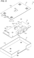
Fig. 5 is an exploded perspective view of a controller. -
Fig. 6 is a view schematically showing a combination of the power supply module and the controller. -
Fig. 7 is a diagram schematically showing a method for providing a power supply device. - One embodiment of a power supply device will be described with reference to the drawings.
- A
power supply device 1 according to the present embodiment is mounted on, for example, an electric power steering device of a vehicle. The electric power steering device assists steering operation of a driver by applying a rotational force of a motor as a steering assist force to a steering mechanism that steers steered wheels based on operation of a steering wheel of the driver. Thepower supply device 1 functions as an auxiliary power supply device that is provided on a power supply path between a main power supply and the motor serving as a power supply target of a power supply, thereby boosting a voltage of the main power supply or backing up the power supply the main power supply fails. - As shown in
Figs. 1A and 1B , thepower supply device 1 has a substantially rectangular parallelepiped shape as a whole, and includes apower supply module 10 that can be charged and discharged, and acontroller 20 that controls charging and discharging of thepower supply module 10. Thepower supply device 1 is formed by combining thepower supply module 10 and thecontroller 20 via a power supply moduleside connection portion 100 and a controllerside connection portion 110, which will be described below. - As shown in
Fig. 2 , thepower supply module 10 includes atray unit 11, atray lid portion 12, abalance board 13, acover 14 and amodule bottom plate 15. - The
tray unit 11 is formed by stacking a plurality of (four inFig. 2 ) plate-shaped tray portions 30 in a plate thickness direction, and has a rectangular parallelepiped shape. The fourtray portions 30 have the same configuration. - As shown in
Fig. 4 , thetray portion 30 has a rectangular plate-shaped tray base 31 having long sides and short sides. Thetray base 31 is formed of a non-conductive material such as resin. Aperipheral wall 31a extending on one side in the plate thickness direction is provided on a peripheral edge of thetray base 31. Anaccommodation portion 31b is formed in thetray base 31 by a surface of thetray base 31 where theperipheral wall 31a extends and inner wall surfaces of theperipheral wall 31a. Theaccommodation portion 31b accommodates a rectangular plate-shaped capacitor 32 having long sides and short sides, and a rectangular plate-shaped terminal portion 33 having long sides and short sides. - The
capacitor 32 is accommodated such that side surfaces of thecapacitor 32 of a pair of long sides and a side surface of thecapacitor 32 of one short side orthogonal to the plate thickness direction are along the inner wall surfaces of theperipheral wall 31a of the pair of long sides and the inner wall surface of theperipheral wall 31a of one short side. Thecapacitor 32 has a positive electrode plate and a negative electrode plate. In the present embodiment, thecapacitor 32 is a lithium ion capacitor. The lithium ion capacitor has high heat resistance, a long service life, a favorable charging and discharging performance, high energy density and high safety. - The
terminal portion 33 is accommodated such that a side surface of theterminal portion 33 of one long side orthogonal to the plate thickness direction are along the inner wall surfaces of theperipheral wall 31a of the pair of long sides and the inner wall surface of theperipheral wall 31a of the other short side. The extending direction of theterminal portion 33 extends along the short side of thetray base 31. Both surfaces of theterminal portion 33 in the thickness direction are partially exposed from the thickness direction of thetray base 31. The positive electrode plate of thecapacitor 32 is connected to one end surface of theterminal portion 33 in the plate thickness direction by welding or the like. - Two
coupling portions 34 are provided on an outer wall surface of theperipheral wall 31a of each of the pair of long sides of thetray base 31. Thecoupling portion 34 includes anengaging portion 34a engageable with an engagedportion 34b provided on thecoupling portion 34 of anothertray portion 30, and an engagedportion 34b engageable with anengaging portion 34a provided on thecoupling portion 34 of anothertray portion 30. In addition, abus bar hole 35 through which afirst bus bar 41 described below is inserted is provided on an outer wall surface of the short side of theperipheral wall 31a on a side where theterminal portion 33 of thetray base 31 is provided so as to protrude outward. - The
tray portions 30 configured as described above are stacked to a side where thecapacitor 32 of onetray portion 30 is exposed from a side where thecapacitor 32 of theother tray portion 30 is not exposed in the plate thickness direction. In this case, theengaging portion 34a of theother tray portion 30 is engaged with the engagedportion 34b of onetray portion 30, whereby one and the othertray portions 30 are assembled to each other. At the same time, theterminal portion 33 exposed in the plate thickness direction of onetray portion 30 and theterminal portion 33 exposed in the plate thickness direction of theother tray portion 30 are electrically connected by abutting each other via thecapacitor 32, that is, the positive and negative electrode plates of thecapacitor 32. Thereby, thecapacitors 32 are electrically connected in series. In addition, thebus bar holes 35 are communicated with each other in the plate thickness direction between onetray portion 30 and theother tray portion 30. As in an example shown inFig. 2 , when fourtray portions 30 are stacked in the plated thickness direction and fourcapacitors 32 are connected in series, a magnitude of a discharge voltage serving as a power supply performance of thetray unit 11 is a sum of discharge voltages of the fourcapacitors 32. For example, when a discharge voltage of onecapacitor 32 is about 3V (volts), the magnitude of the discharge voltage of thetray unit 11 will be about 12V. - As shown in
Fig. 2 , thetray lid portion 12 is placed on thetray portion 30 in which thecapacitor 32 is exposed in thetray unit 11, that is, thetray portion 30 stacked on the uppermost side when the plate thickness direction is an upper-lower direction. Thetray lid portion 12 has a rectangular plate-shapedtray lid base 40 having long sides and short sides. Thetray lid base 40 is formed of a non-conductive material such as resin. - Two
engaging portions 42 are provided on a side surface of each of the pair of long sides of thetray lid base 40. The engagingportion 42 has a configuration the same as the engagingportion 34a of thecoupling portion 34 of thetray portion 30, and is configured to be engageable with the engagedportion 34b provided in thetray portion 30. Thefirst bus bar 41 is connected to a side surface of one short side of thetray lid base 40. - One end of the
first bus bar 41 is connected to thetray lid base 40, and the other end thereof extends in the plate thickness direction. A length of thefirst bus bar 41 is set such that a tip end of the other end protrudes from thepower supply module 10 in a stacking direction. The one end of thefirst bus bar 41 connected to thetray lid base 40 is exposed from thetray lid base 40 on a side where thefirst bus bar 41 extends toward the other end of thefirst bus bar 41. - The
module bottom plate 15 is placed on thetray portion 30 in which thecapacitor 32 is not exposed in thetray unit 11, that is, thetray portion 30 stacked on the lowermost side when the plate thickness direction is the upper-lower direction. Themodule bottom plate 15 has a rectangular plate-shapedhousing base 50 having long sides and short sides. Thehousing base 50 is formed of a non-conductive material such as resin. Aperipheral wall 50a extending on one side in the plate thickness direction is provided on a peripheral edge of thehousing base 50. Anaccommodation portion 50b is formed in thehousing base 50 by a surface of thehousing base 50 where theperipheral wall 50a extends and inner wall surfaces of theperipheral wall 50a. A plate-shapedbalance board 13 is fixed to theaccommodation portion 50b by a fastening member such as a screw. - The
balance board 13 is used to adjust the discharge voltage of eachcapacitor 32 of thetray unit 11 so as to suppress a variation in the discharge voltage. Acontrol element 13a that functions to adjust the discharge voltage of eachcapacitor 32 is provided on one end surface of thebalance board 13 in the plate thickness direction. In the present embodiment, thecontrol element 13a controls the discharge voltage of eachcapacitor 32 to be the lowest discharge voltage of thecapacitor 32 when adjusting the discharge voltage of eachcapacitor 32. - A power module side
communication connection portion 13b for electrical communication between thecontrol element 13a and thecontroller 20 is provided on the other end surface of thebalance board 13 in the plate thickness direction. Thebalance board 13 is fixed such that the other end surface side in the plate thickness direction faces ahousing base 50 side. The power module sidecommunication connection portion 13b is configured to protrude from a surface opposite to a direction in which theperipheral wall 50a of thehousing base 50 extends through aconnection portion hole 50c provided in a center portion of thehousing base 50. - Two engaged
portions 51 are provided on an outer wall surface of theperipheral wall 50a of each of the pair of long sides of thehousing base 50. The engagedportion 51 has a configuration the same as the engagedportion 34b of thecoupling portion 34 of thetray portion 30, and is configured to be engageable with the engagingportion 34a provided in thetray portion 30. Asecond bus bar 52 is connected to a portion on one short side of thehousing base 50. - One end of the
second bus bar 52 is connected to thehousing base 50, and the other end thereof extends in the plate thickness direction. A length of thesecond bus bar 52 is set such that a tip end of the other end protrudes from thepower supply module 10 in the stacking direction. One end of thesecond bus bar 52 connected to thehousing base 50 is exposed on a side opposite to a side where the other end of thesecond bus bar 52 of thehousing base 50 extends. In addition, abus bar hole 53 through which thefirst bus bar 41 is inserted in a state adjacent to thesecond bus bar 52 is provided at a portion on one short side of thehousing base 50. - The
tray lid portion 12 configured as described above is stacked on thetray portion 30 stacked on the uppermost side of thetray unit 11 from a side where thefirst bus bar 41 extends in the plate thickness direction. In this case, the engagingportion 42 of thetray lid portion 12 is engaged with the engagedportion 34b of thetray portion 30 stacked on the uppermost side, whereby thetray lid portion 12 and thetray portion 30 stacked on the uppermost side are assembled to each other. At the same time, one end of thefirst bus bar 41 exposed on the side where the other end of thefirst bus bar 41 extends and theterminal portion 33 exposed in the plate thickness direction of thetray portion 30 stacked on the uppermost side are electrically connected by abutting each other via thecapacitor 32, that is, the positive and negative electrode plates of thecapacitor 32. Thefirst bus bar 41 of thetray lid portion 12 is inserted into the bus bar holes 35 communicated with each other between thetray portions 30 of thetray unit 11. - In addition, the
module bottom plate 15 configured as described above is stacked below thetray portion 30 stacked on the lowermost side of thetray unit 11 from the side opposite to the side where thesecond bus bar 52 extends in the plate thickness direction. In this case, the engagingportion 34a of thetray portion 30 stacked on the lowermost side is engaged with the engagedportion 51 of themodule bottom plate 15, whereby themodule bottom plate 15 and thetray portion 30 stacked on the lowermost side are assembled to each other. At the same time, one end of thesecond bus bar 52 exposed on the side opposite to the side where the other end of thesecond bus bar 52 extends and theterminal portion 33 exposed in the plate thickness direction of thetray portion 30 stacked on the lowermost side are electrically connected by abutting each other. Thebus bar hole 53 of themodule bottom plate 15 is communicated with the bus bar holes 35 communicated with each other between thetray portions 30 of thetray unit 11 in the plate thickness direction. Thefirst bus bar 41 of thetray lid portion 12 is inserted into thebus bar hole 53. - In this case, as shown in
Fig. 3 , from the side where thesecond bus bar 52 of themodule bottom plate 15 extends, the tip end of the other end of thefirst bus bar 41 of thetray lid portion 12 and the tip end of the other end of thesecond bus bar 52 of themodule bottom plate 15 protrude, and the power supply module sidecommunication connection portion 13b of thebalance board 13 protrudes. Oneprotrusion 54 serving as a portion protruding from other portions is provided in each of four corners on a surface of themodule bottom plate 15 on the side where thesecond bus bar 52 extends. - As shown in
Fig. 2 and3 , to a structure in which thetray unit 11, thetray lid portion 12, thebalance board 13 and themodule bottom plate 15 are assembled, a bottomed box-shapedcover 14 is assembled from anopening 14a side so as to accommodate the structure. Thecover 14 is fixed to the side opposite to the side opposite to the side where thefirst bus bar 41 of thetray lid portion 12 extends by a fastening member such as a screw. Thereby, thepower supply module 10 is formed. - As shown in
Fig. 5 , thecontroller 20 includes acontroller housing 21, acontrol board 22 and acontroller lid portion 23. - The
controller housing 21 has a bottomed box shape, and the plate-shapedcontrol board 22 is fixed therein by a fastening member such as a screw. Thecontrol board 22 controls charging and discharging of eachcapacitor 32 of thetray unit 11. Acontrol element 22a that functions to control charging and discharging of eachcapacitor 32 is provided on one end surface of thecontrol board 22 in the plate thickness direction. In the example shown inFig. 2 , when controlling charging and discharging of eachcapacitor 32, thecontrol element 22a performs control so as to boost the voltage of the main power supply and back up the power supply when the main power supply fails. - A controller side
communication connection portion 22b for electrical communication between thecontrol element 22a and thecontrol element 13a of thepower supply module 10 is provided on one end surface of thecontrol board 22 in the plate thickness direction. The controller sidecommunication connection portion 22b is provided at a position corresponding to the power module sidecommunication connection portion 13b when thepower supply module 10 and thecontroller 20 are assembled. - A controller side power
supply connection portion 22c for electrical connection with thefirst bus bar 41 and thesecond bus bar 52 is provided on one end surface of thecontrol board 22 in the plate thickness direction. The controller side powersupply connection portion 22c is provided at a position corresponding to tip ends of the other end side of thefirst bus bar 41 and thesecond bus bar 52 when thepower supply module 10 and thecontroller 20 are assembled. - An external
communication connection portion 22d for electrical communication with an external device or the like (not shown) is provided on one end surface of thecontrol board 22 in the plate thickness direction. The externalcommunication connection portion 22d is provided on one end surface of thecontrol board 22 so as to extend in a direction orthogonal to the plate thickness direction from one long side. - A power
supply connection portion 22e for electrical connection with the main power supply (not shown) is provided on one end surface of thecontrol board 22 in the plate thickness direction. The powersupply connection portion 22e is provided on one end surface of thecontrol board 22 so as to extend in a direction orthogonal to the plate thickness direction from one long side in a state adjacent to the externalcommunication connection portion 22d. - The
control board 22 is fixed such that a one end surface side thereof in the plate thickness direction faces anopening 21a side of thecontroller housing 21. In this case, the externalcommunication connection portion 22d and the powersupply connection portion 22e protrude from a side surface of a side wall of thecontroller housing 21 through aconnection portion hole 21b provided in the side wall of one long side of thecontroller housing 21. - As shown in
Fig. 5 , thecontroller lid portion 23 has a rectangular plate-shapedcontroller lid base 23a having long sides and short sides. Thecontroller lid base 23a is formed of a non-conductive material such as resin. Aconnection portion hole 23b penetrating in the plate thickness direction is provided at a center of thecontroller lid base 23a. Theconnection portion hole 23b is provided at a position corresponding to the controller sidecommunication connection portion 22b.Bus bar holes controller lid base 23a. Thebus bar holes supply connection portion 22c. Onerecess 23e serving as a portion recessed from other portions is provided in each of the four corners on one end surface of thecontroller lid portion 23 in the plate thickness direction. Eachrecess 23e is provided at a position corresponding to eachprotrusion 54 of themodule bottom plate 15 when thepower supply module 10 and thecontroller 20 are assembled. - The
controller lid portion 23 configured as described above is assembled to theopening 21a side of thecontroller housing 21 so as to accommodate a structure in which thecontroller housing 21 and thecontrol board 22 are assembled from a the other end surface side opposite to a side where therecesses 23e are provided, in the plate thickness direction. Thecontroller lid portion 23 is fixed to thecontroller housing 21 by a fastening member such as a screw. Thereby, thecontroller 20 is formed. - As shown in
Figs. 1A and 1B , thepower supply module 10 and thecontroller 20 are assembled in a state in which amodule bottom plate 15 side of thepower supply module 10 and acontroller lid portion 23 side of thecontroller 20 face each other. - In this case, as shown in
Figs. 3 and5 , the power module sidecommunication connection portion 13b protruding from themodule bottom plate 15 side of thepower supply module 10 is fitted and electrically connected to the controller sidecommunication connection portion 22b of thecontrol board 22 through theconnection portion hole 23b provided in thecontroller lid portion 23. Thefirst bus bar 41 and thesecond bus bar 52 protruding from themodule bottom plate 15 side of thepower supply module 10 are fitted and electrically connected to the controller side powersupply connection portion 22c of thecontrol board 22 through thebus bar holes controller lid portion 23. Theprotrusions 54 protruding from themodule bottom plate 15 side of thepower supply module 10 and therecesses 23e of thecontroller lid portion 23 are unevenly fitted to each other. Thereby, thepower supply device 1 is formed. - The above description has described the
power supply device 1 having a power supply performance in which the fourcapacitors 32 are connected in series and a function of boosting the voltage of the main power supply and backing up the power supply when the main power supply fails. - In the
power supply device 1 according to the present embodiment, in addition to the example shown inFig. 2 , thepower supply module 10 having different power supply performances can be formed by adopting thetray unit 11 in which the number of thetray portions 30, that is, thecapacitors 32 is changed. - For example, as shown in
Fig. 6 , by adopting thetray unit 11 in which the number of thecapacitors 32 is changed to two, thepower supply module 10 having a power supply performance in which the magnitude of the discharge voltage is about 6V when the discharge voltage of onecapacitor 32 is about 3V can be formed. By adopting thetray unit 11 in which the number of thecapacitors 32 is changed to eight, thepower supply module 10 having a power supply performance in which the magnitude of the discharge voltage is about 24V when the discharge voltage of onecapacitor 32 is about 3V can be formed. In addition, many variations of thepower supply module 10 having three, five and thelike capacitors 32 can be considered. - In this way, in many variations of the
power supply module 10, the number of thetray portions 30 is changed to a desired number, and the length of thefirst bus bar 41 of thetray lid portion 12 is changed such that the tip end of the other end protrudes from thepower supply module 10 in the stacking direction, and the number of thecontrol elements 13a of thebalance board 13 is changed according to the number of thetray portions 30. In many variations of thepower supply module 10, a size of thecover 14 is changed such that thetray unit 11 in which the number of thetray portions 30 is changed can be accommodated. On the other hand, in many variations of thepower module 10, the same configurations of the power module sidecommunication connection portion 13b of thebalance board 13 and themodule bottom plate 15 are used. That is, in many variations of thepower module 10, configurations are made common, in which the tip end of the other end of thefirst bus bar 41 of thetray lid portion 12, the tip end of the other end of thesecond bus bar 52 of themodule bottom plate 15, the power supply module sidecommunication connection portion 13b of thebalance board 13 and theprotrusions 54 of themodule bottom plate 15, all protrude from the side where thesecond bus bar 52 of themodule bottom plate 15 extends. The common configurations in thesepower supply modules 10, that is, thefirst bus bar 41 of thetray lid portion 12, thesecond bus bar 52 of themodule bottom plate 15, the power supply module sidecommunication connection portion 13b of thebalance board 13 and theprotrusions 54 of themodule bottom plate 15, correspond to the common power supply module side connection portion 100 (seeFig. 1B and the like). - In addition to the example shown in
Fig. 2 , in thepower supply device 1 according to the present embodiment, thecontroller 20 having a different function can be formed by adopting thecontrol board 22 in which a function of thecontrol element 22a is changed. - For example, as shown in
Fig. 6 , many variations of thecontroller 20, in which the function of thecontrol element 22a is changed to only boost the voltage of the main power supply or to only back up the power supply when the main power supply fails, can be considered. - In this way, in many variations of the
controller 20, a processing program stored in a ROM (not shown) of thecontrol board 22 is changed to a processing program having a desired function. On the other hand, in many variations of thecontroller 20, the same configurations of the controller sidecommunication connection portion 22b, the controller side powersupply connection portion 22c, the externalcommunication connection portion 22d, the powersupply connection portion 22e, thecontroller housing 21 and thecontroller lid portion 23 are used. That is, configurations are made common, in which the power supply module sidecommunication connection portion 13b of thepower supply module 10 can be fitted to the controller sidecommunication connection portion 22b of thecontrol board 22, thefirst bus bar 41 and thesecond bus bar 52 of thepower supply module 10 can be fitted to the controller sidepower connection portion 22c of thecontrol board 22, and theprotrusions 54 can be respectively fitted to therecesses 23e. The common configurations in thesecontrollers 20, that is, the controller sidecommunication connection portion 22b of thecontrol board 22, the controller side powersupply connection portion 22c of thecontrol board 22, and therecesses 23e of thecontroller lid portion 23, correspond to the common controller side connection portion 110 (seeFig. 1B and the like). - That is, as shown in
Fig. 6 , in the present embodiment, any one of many conceivable variations of thepower supply module 10 can be combined with many conceivable variations of thecontroller 20. Therefore, onepower supply module 10 having a desired power supply performance is selected from many conceivable variations of thepower supply module 10, and onecontroller 20 having a desired function is selected from many conceivable variations of thecontroller 20, and a desiredpower supply device 1 can be formed by combining thepower supply module 10 and thecontroller 20. In a not-claimed example, thepower supply device 1 having a combination of only thepower supply module 10 can be configured without combining thecontroller 20 with thepower supply module 10. - A method for providing the
power supply device 1 according to the present embodiment will be described in detail below. - In the present embodiment, many conceivable variations of the
power supply module 10 as described above are manufactured and prepared in advance, and many conceivable variations of thecontroller 20 as described above are manufactured and prepared in advance. In this state, thepower supply device 1 is provided according to the following flow. - Specifically, as shown in
Fig. 7 , when an order indicating requirements such as the power supply performance of thepower supply module 10 and the function of thecontroller 20 is received from a customer, a power supply module selection step and a controller selection step are respectively performed in order to select a desiredpower supply module 10 and a desiredcontroller 20 according to the requirements. - In the power supply module selection step, the
power supply module 10 configured to have the power supply performance according to the requirement of the received order is selected from many variations of thepower supply module 10 manufactured and prepared in advance. - In the controller selection step, the
controller 20 having the function according to the requirement of the received order is selected from many variations of thecontroller 20 manufactured and prepared in advance. In the controller selection step, if a requirement that does not require a controller is indicated as the requirement of the received order, nocontroller 20 is selected. - After performing the power supply module selection step and the controller selection step, a combination step of combining the
power supply module 10 and thecontroller 20 selected in the selection steps is performed, and thepower supply device 1 is provided by performing the combination step. When thecontroller 20 is not selected in the controller selection step, thepower supply module 10 selected in the power supply module selection step is provided as thepower supply device 1. In this case, the combination step is omitted. - The operation and effects of the present embodiment will be described.
- (1) According to the present embodiment, any one of many conceivable variations of the
power supply module 10 can be combined with any one of many conceivable variations of thecontroller 20. Therefore, onepower supply module 10 having a desired power supply performance is selected from many conceivable variations of thepower supply module 10, and onecontroller 20 having a desired function is selected from many conceivable variations of thecontroller 20, and a desiredpower supply device 1 can be formed by combining thepower supply module 10 and thecontroller 20. Therefore, when the desiredpower supply device 1 is provided, the plurality ofpower supply modules 10 having different power supply performances may be manufactured and prepared in advance, and the plurality ofcontrollers 20 having different functions may be manufactured and prepared in advance. Compared with a case where thepower supply device 1 is redesigned for each use, the number of steps required to provide thepower supply device 1 can be prevented from increasing. - (2) The
power supply module 10 having a different discharge voltage as the power supply performance can be provided, and a desired discharge voltage can appropriately deal with a different need. - (3) The
controller 20 having a different function of boosting the voltage of the main power supply or backing up the power supply when the main power supply fails as the function can be provided, and a desired function of boosting the voltage of the main power supply or backing up the power supply when the main power supply fails can appropriately deal with a different need. - (4) According to the not-claimed example, only the
power supply module 10 can be provided as thepower supply device 1, which can appropriately deal with a need for only thepower supply module 10. - (5) When use of the
power supply device 1 in a current use ends, the combination of thepower supply module 10 and thecontroller 20 is released, and thepower supply module 10 can be reused in a next use. Since the power supply moduleside connection portion 100 and the controllerside connection portion 110 are common, thepower supply module 10 can be combined with thecontroller 20 having a desired function in the next use. During reuse, thetray portion 30 can be reused individually by releasing engagement between the engagedportion 34b and the engagingportion 34a. In particular, since a lithium ion capacitor is adopted as thecapacitor 32, whose lifetime is long, there may be many opportunities for reuse. Therefore, a need to reuse thepower supply device 1 can be appropriately dealt with. In addition, thetray portion 30 can be individually detached from thetray unit 11, which can appropriately deal with repair or replacement of thetray portion 30 in units. - (6) In the present embodiment, since the
capacitor 32 is formed in a rectangular plate shape, waste of space when thepower supply device 1 is mounted can be reduced as compared with a case where an electric double-layer capacitor generally having a cylindrical shape is used. - The present embodiment may be modified as follows. In addition, the following other embodiments can be combined with each other as long as there is no technical contradiction. Many conceivable variations of the
power supply module 10 may be prepared in advance, and these may be arranged in a store or the like. Therefore, the method for providing thepower supply module 10 may be adopted to allow the customer to select a desiredpower supply module 10 from many prepared variations of thepower supply module 10. Many conceivable variations of thecontroller 20 may be prepared in advance, and these may be arranged in a store or the like to allow the customer to select a desiredcontroller 20 from many prepared variations of thecontroller 20. Even when such a providing method is adopted, effects the same as those of the above embodiment can be obtained. - When the use of the
power supply device 1 in the current use is completed, the combination of thepower supply module 10 and thecontroller 20 is released, and thecontroller 20 may be reused in the next use. - The function of the
controller 20 may be a communication function of communicating information such as a charging state of thepower supply module 10 with the external device. The function of thecontroller 20 may be presence or absence of the communication function with the external device. In this case, thecontrol board 22 may change presence or absence of the externalcommunication connection portion 22d. That is, at least the power supply moduleside connection portion 100 and the controllerside connection portion 110 may be common, and the externalcommunication connection portion 22d and the powersupply connection portion 22e may not be common in thecontrol board 22. That is, as a variation of the function of thecontroller 20, the externalcommunication connection portion 22d and the powersupply connection portion 22e may be prepared to have different configurations. - The power supply performance of the
power supply module 10 may include a capacitor capacity of thepower supply module 10, or may include a current amount of thepower supply module 10. - The
power supply module 10 may be used as the main power supply. In this case, the function of thecontroller 20 includes a function of operating thepower supply module 10 as the main power supply. - The overall shape of the
power supply device 1 is not limited to the rectangular parallelepiped shape, and may be, for example, a cylindrical shape. - In the
power supply module 10, an electric double-layer capacitor (EDLC), a lithium ion battery, a lead storage battery or the like may be used as a power supply instead of thecapacitor 32. Even in these cases, effects the same as those of the above embodiment can be obtained. - The
power supply device 1 may be applied to an uninterruptible power supply device, may be mounted on an automated guided vehicle, may be mounted on a transmission line, or may be mounted on an industrial machine.
Claims (6)
- A power supply device comprising:a combination of one power supply module (10) of a plurality of power supply modules configured to have different power supply performances and one controller (20) of a plurality of controllers configured to have different functions, which are selectively combined, wherein each power supply module comprises a tray unit (11) having a different number of stacked tray portions, each tray portion (30) accommodating a plate-shaped power supply (32) such as a capacitor, and a plate-shaped terminal portion (33),the capacitors are electrically connected in series via the plate-shaped terminal portions, and in each tray unit a first bus bar (41) is connected to a tray lid portion (12) stacked on the uppermost tray portion and is electrically connected to the plate-shaped terminal portion of the uppermost power supply via the capacitor, and a second bus bar (52) is connected to a module bottom plate (15) stacked below the lowermost tray portion and is electrically connected to the plate-shaped terminal portion of the lowermost plate-shaped power supply (32),wherein each of the plurality of power supply modules comprises a power supply module side connection portion (100) common to the plurality of power supply modules and comprising the first and the second busbar, and each of the plurality of controllers (20) comprises a controller side connection portion (110) common to the plurality of controllers, comprises a first and a second bus bar hole (23c, 23d), and is configured to be connectable to the power supply module side connection portion (100), to allow that the one power supply module and the one controller are selectively combined, andfor each power supply module (10) the first and second bus bars (41, 52) protrude from the power supply module in the stacking direction and are configured to be fitted and electrically connectable to the first and second bus bar holes (23c, 23d) provided in a controller lid portion (23) of each controller.
- The power supply device according to claim 1, wherein the power supply performances are configured to be related to discharge voltages of the power supply modules (10).
- The power supply device according to claim 1 or 2,wherein the power supply device is configured to serve as an auxiliary power supply device provided on a power supply path between a main power supply and a power supply target of a power supply, andwherein the functions are configured to control charging and discharging of the power supply module (10), including a function that is configured to boost a voltage of the main power supply through the charging and discharging of the power supply module and a function that is configured to back up the power supply at a time of failure of the main power supply through the charging and discharging of the power supply module.
- A method for providing the power supply device of any one of the previous claims, comprising:a power supply module selection process in which the one power supply module (10) is selected from the plurality of power supply modules having the different power supply performances, each of the plurality of power supply modules comprising the power supply module side connection portion (100) common to the plurality of power supply modules; anda controller selection process in which the one controller (20) is selected from the plurality of controllers having different functions, each of the plurality of controllers comprising the controller side connection portion (110) common to the plurality of controllers and connectable to the power supply module side connection portion (100).
- The method for providing the power supply device according to claim 4,
wherein the power supply performances of the power supply modules (10) to be selected in the power supply module selection process are related to discharge voltages of the power supply modules. - The method for providing the power supply device according to claims 4 or 5,wherein the power supply device serves as an auxiliary power supply device provided on a power supply path between a main power supply and a power supply target of a power supply, andwherein the functions of the controllers (20) to be selected in the controller selection process are to control charging and discharging of the power supply module, including a function of boosting a voltage of the main power supply through the charging and discharging of the power supply module (10) and a function of backing up the power supply at a time of failure of the main power supply through the charging and discharging of the power supply module (10).
Applications Claiming Priority (1)
| Application Number | Priority Date | Filing Date | Title |
|---|---|---|---|
| JP2019027813A JP7193372B2 (en) | 2019-02-19 | 2019-02-19 | Power supply and method of providing power supply |
Publications (2)
| Publication Number | Publication Date |
|---|---|
| EP3699978A1 EP3699978A1 (en) | 2020-08-26 |
| EP3699978B1 true EP3699978B1 (en) | 2023-09-27 |
Family
ID=69784010
Family Applications (1)
| Application Number | Title | Priority Date | Filing Date |
|---|---|---|---|
| EP20157856.4A Active EP3699978B1 (en) | 2019-02-19 | 2020-02-18 | Power supply device and method for providing the power supply device |
Country Status (4)
| Country | Link |
|---|---|
| US (1) | US11404900B2 (en) |
| EP (1) | EP3699978B1 (en) |
| JP (1) | JP7193372B2 (en) |
| CN (1) | CN111585316B (en) |
Family Cites Families (17)
| Publication number | Priority date | Publication date | Assignee | Title |
|---|---|---|---|---|
| US4652769A (en) * | 1984-02-14 | 1987-03-24 | Ion Tech, Inc. | Module power supply |
| JP3498696B2 (en) * | 2000-05-29 | 2004-02-16 | オムロン株式会社 | Power supply module and power supply unit used therefor |
| WO2006068373A1 (en) * | 2004-12-24 | 2006-06-29 | Lg Chem, Ltd. | Secondary battery module |
| JP2008062712A (en) | 2006-09-05 | 2008-03-21 | Jtekt Corp | Motor control device |
| US7531270B2 (en) | 2006-10-13 | 2009-05-12 | Enerdel, Inc. | Battery pack with integral cooling and bussing devices |
| US20080193830A1 (en) | 2006-10-13 | 2008-08-14 | Enerdel, Inc. | Battery assembly with temperature control device |
| JP5254568B2 (en) * | 2007-05-16 | 2013-08-07 | 日立ビークルエナジー株式会社 | Cell controller, battery module and power supply system |
| JP5626852B2 (en) * | 2010-05-19 | 2014-11-19 | Necエナジーデバイス株式会社 | Power supply |
| JP2014143771A (en) * | 2011-05-18 | 2014-08-07 | Sanyo Electric Co Ltd | Power supply system, identification information setting method for power supply system, and battery unit |
| KR101114255B1 (en) * | 2011-12-08 | 2012-03-06 | 주식회사 디와이티오코리아 | Vehicles equipped with a spare battery |
| KR200473025Y1 (en) * | 2012-05-09 | 2014-06-10 | 휴지 테크놀로지 컴퍼니 리미티드 | Portable external power-supplying device |
| JP6418239B2 (en) * | 2014-06-03 | 2018-11-07 | 株式会社村田製作所 | Power supply apparatus and power supply method |
| JP6242008B2 (en) * | 2014-06-25 | 2017-12-06 | Fdk株式会社 | Uninterruptible power system |
| JP6655806B2 (en) * | 2014-06-26 | 2020-02-26 | パナソニックIpマネジメント株式会社 | Power supply device and lighting device using the same |
| CN204167923U (en) * | 2014-07-30 | 2015-02-18 | 深圳欧陆通电子有限公司 | From charged pool redundant power supply |
| US10328354B2 (en) * | 2017-02-27 | 2019-06-25 | Cardalloon Co Llc | Gift box with self-inflating balloon |
| US11233419B2 (en) * | 2017-08-10 | 2022-01-25 | Zoox, Inc. | Smart battery circuit |
-
2019
- 2019-02-19 JP JP2019027813A patent/JP7193372B2/en active Active
-
2020
- 2020-02-18 EP EP20157856.4A patent/EP3699978B1/en active Active
- 2020-02-18 CN CN202010099572.5A patent/CN111585316B/en active Active
- 2020-02-19 US US16/794,342 patent/US11404900B2/en active Active
Also Published As
| Publication number | Publication date |
|---|---|
| JP7193372B2 (en) | 2022-12-20 |
| CN111585316B (en) | 2025-09-02 |
| JP2020137267A (en) | 2020-08-31 |
| CN111585316A (en) | 2020-08-25 |
| EP3699978A1 (en) | 2020-08-26 |
| US20200266656A1 (en) | 2020-08-20 |
| US11404900B2 (en) | 2022-08-02 |
Similar Documents
| Publication | Publication Date | Title |
|---|---|---|
| US9660230B2 (en) | Battery pack having end plates | |
| JP5394522B2 (en) | Separating type connecting member for manufacturing secondary battery module and method for improving battery module performance by voltage leveling | |
| EP2562842B1 (en) | Battery module | |
| KR100859538B1 (en) | Storage battery device | |
| JP6926770B2 (en) | Battery packs and electrical equipment using battery packs | |
| US8557428B2 (en) | Battery module and battery pack including the same | |
| KR20160077758A (en) | Compact secondary battery module integrated with BMS | |
| JP4568067B2 (en) | Pack battery | |
| US20130207456A1 (en) | Battery cell module, battery, and motor vehicle | |
| JP2008204982A (en) | Capacitor unit | |
| KR100983011B1 (en) | Electrical Connecting Member for Battery Cell Based on Physical Contact Manner | |
| KR20170089226A (en) | Ultra Capacitor Module | |
| EP3699978B1 (en) | Power supply device and method for providing the power supply device | |
| KR20190045611A (en) | PCB busbars used in assembling Lithium battery pack | |
| JP2014514705A (en) | Energy storage assembly and energy storage device | |
| KR20230102738A (en) | Bus bar holder, bus bar assembly and battery module | |
| JP5061430B2 (en) | Battery module | |
| EP2911222B1 (en) | Bus bar module | |
| KR20170044472A (en) | Battery module and battery pack including the same | |
| JP6162414B2 (en) | Battery assembly | |
| KR20180029689A (en) | Intergrated Cartridge for battery cell and Battery Pack having the same | |
| EP3653338B1 (en) | Disassembling tool and battery module using disassembling tool | |
| KR20180012568A (en) | Connector for connecting lead and battery module using the same | |
| EP4439826A2 (en) | Battery pack | |
| US20250379314A1 (en) | Structure and method for fixing battery module to battery pack |
Legal Events
| Date | Code | Title | Description |
|---|---|---|---|
| PUAI | Public reference made under article 153(3) epc to a published international application that has entered the european phase |
Free format text: ORIGINAL CODE: 0009012 |
|
| STAA | Information on the status of an ep patent application or granted ep patent |
Free format text: STATUS: THE APPLICATION HAS BEEN PUBLISHED |
|
| AK | Designated contracting states |
Kind code of ref document: A1 Designated state(s): AL AT BE BG CH CY CZ DE DK EE ES FI FR GB GR HR HU IE IS IT LI LT LU LV MC MK MT NL NO PL PT RO RS SE SI SK SM TR |
|
| AX | Request for extension of the european patent |
Extension state: BA ME |
|
| STAA | Information on the status of an ep patent application or granted ep patent |
Free format text: STATUS: REQUEST FOR EXAMINATION WAS MADE |
|
| 17P | Request for examination filed |
Effective date: 20210225 |
|
| RBV | Designated contracting states (corrected) |
Designated state(s): AL AT BE BG CH CY CZ DE DK EE ES FI FR GB GR HR HU IE IS IT LI LT LU LV MC MK MT NL NO PL PT RO RS SE SI SK SM TR |
|
| RAP3 | Party data changed (applicant data changed or rights of an application transferred) |
Owner name: KYOHO MACHINE WORKS, LTD. Owner name: JTEKT CORPORATION |
|
| REG | Reference to a national code |
Ref country code: DE Ref legal event code: R079 Free format text: PREVIOUS MAIN CLASS: H01M0002100000 Ref country code: DE Ref legal event code: R079 Ref document number: 602020018118 Country of ref document: DE Free format text: PREVIOUS MAIN CLASS: H01M0002100000 Ipc: H01M0010420000 |
|
| GRAP | Despatch of communication of intention to grant a patent |
Free format text: ORIGINAL CODE: EPIDOSNIGR1 |
|
| STAA | Information on the status of an ep patent application or granted ep patent |
Free format text: STATUS: GRANT OF PATENT IS INTENDED |
|
| RIC1 | Information provided on ipc code assigned before grant |
Ipc: H02J 9/06 20060101ALI20230328BHEP Ipc: H02J 7/34 20060101ALI20230328BHEP Ipc: H01M 10/42 20060101AFI20230328BHEP |
|
| INTG | Intention to grant announced |
Effective date: 20230420 |
|
| GRAS | Grant fee paid |
Free format text: ORIGINAL CODE: EPIDOSNIGR3 |
|
| GRAA | (expected) grant |
Free format text: ORIGINAL CODE: 0009210 |
|
| STAA | Information on the status of an ep patent application or granted ep patent |
Free format text: STATUS: THE PATENT HAS BEEN GRANTED |
|
| RIN1 | Information on inventor provided before grant (corrected) |
Inventor name: KAWANO, MASAFUMI Inventor name: SHINODA, SATOSHI Inventor name: KOMATSUBARA, YUKIHIRO Inventor name: MIO, TAKUMI Inventor name: SUGIYAMA, TOYOKI Inventor name: SAWADA, SHINICHI Inventor name: NISHI, KOJI Inventor name: ONISHI, TAKANORI |
|
| AK | Designated contracting states |
Kind code of ref document: B1 Designated state(s): AL AT BE BG CH CY CZ DE DK EE ES FI FR GB GR HR HU IE IS IT LI LT LU LV MC MK MT NL NO PL PT RO RS SE SI SK SM TR |
|
| RAP3 | Party data changed (applicant data changed or rights of an application transferred) |
Owner name: KYOHO MACHINE WORKS, LTD. Owner name: JTEKT CORPORATION |
|
| REG | Reference to a national code |
Ref country code: GB Ref legal event code: FG4D |
|
| REG | Reference to a national code |
Ref country code: CH Ref legal event code: EP |
|
| REG | Reference to a national code |
Ref country code: DE Ref legal event code: R096 Ref document number: 602020018118 Country of ref document: DE |
|
| REG | Reference to a national code |
Ref country code: IE Ref legal event code: FG4D |
|
| REG | Reference to a national code |
Ref country code: LT Ref legal event code: MG9D |
|
| PG25 | Lapsed in a contracting state [announced via postgrant information from national office to epo] |
Ref country code: GR Free format text: LAPSE BECAUSE OF FAILURE TO SUBMIT A TRANSLATION OF THE DESCRIPTION OR TO PAY THE FEE WITHIN THE PRESCRIBED TIME-LIMIT Effective date: 20231228 |
|
| PG25 | Lapsed in a contracting state [announced via postgrant information from national office to epo] |
Ref country code: SE Free format text: LAPSE BECAUSE OF FAILURE TO SUBMIT A TRANSLATION OF THE DESCRIPTION OR TO PAY THE FEE WITHIN THE PRESCRIBED TIME-LIMIT Effective date: 20230927 Ref country code: RS Free format text: LAPSE BECAUSE OF FAILURE TO SUBMIT A TRANSLATION OF THE DESCRIPTION OR TO PAY THE FEE WITHIN THE PRESCRIBED TIME-LIMIT Effective date: 20230927 Ref country code: NO Free format text: LAPSE BECAUSE OF FAILURE TO SUBMIT A TRANSLATION OF THE DESCRIPTION OR TO PAY THE FEE WITHIN THE PRESCRIBED TIME-LIMIT Effective date: 20231227 Ref country code: LV Free format text: LAPSE BECAUSE OF FAILURE TO SUBMIT A TRANSLATION OF THE DESCRIPTION OR TO PAY THE FEE WITHIN THE PRESCRIBED TIME-LIMIT Effective date: 20230927 Ref country code: LT Free format text: LAPSE BECAUSE OF FAILURE TO SUBMIT A TRANSLATION OF THE DESCRIPTION OR TO PAY THE FEE WITHIN THE PRESCRIBED TIME-LIMIT Effective date: 20230927 Ref country code: HR Free format text: LAPSE BECAUSE OF FAILURE TO SUBMIT A TRANSLATION OF THE DESCRIPTION OR TO PAY THE FEE WITHIN THE PRESCRIBED TIME-LIMIT Effective date: 20230927 Ref country code: GR Free format text: LAPSE BECAUSE OF FAILURE TO SUBMIT A TRANSLATION OF THE DESCRIPTION OR TO PAY THE FEE WITHIN THE PRESCRIBED TIME-LIMIT Effective date: 20231228 Ref country code: FI Free format text: LAPSE BECAUSE OF FAILURE TO SUBMIT A TRANSLATION OF THE DESCRIPTION OR TO PAY THE FEE WITHIN THE PRESCRIBED TIME-LIMIT Effective date: 20230927 |
|
| REG | Reference to a national code |
Ref country code: NL Ref legal event code: MP Effective date: 20230927 |
|
| REG | Reference to a national code |
Ref country code: AT Ref legal event code: MK05 Ref document number: 1616324 Country of ref document: AT Kind code of ref document: T Effective date: 20230927 |
|
| PG25 | Lapsed in a contracting state [announced via postgrant information from national office to epo] |
Ref country code: NL Free format text: LAPSE BECAUSE OF FAILURE TO SUBMIT A TRANSLATION OF THE DESCRIPTION OR TO PAY THE FEE WITHIN THE PRESCRIBED TIME-LIMIT Effective date: 20230927 |
|
| PG25 | Lapsed in a contracting state [announced via postgrant information from national office to epo] |
Ref country code: IS Free format text: LAPSE BECAUSE OF FAILURE TO SUBMIT A TRANSLATION OF THE DESCRIPTION OR TO PAY THE FEE WITHIN THE PRESCRIBED TIME-LIMIT Effective date: 20240127 |
|
| PG25 | Lapsed in a contracting state [announced via postgrant information from national office to epo] |
Ref country code: AT Free format text: LAPSE BECAUSE OF FAILURE TO SUBMIT A TRANSLATION OF THE DESCRIPTION OR TO PAY THE FEE WITHIN THE PRESCRIBED TIME-LIMIT Effective date: 20230927 |
|
| PG25 | Lapsed in a contracting state [announced via postgrant information from national office to epo] |
Ref country code: ES Free format text: LAPSE BECAUSE OF FAILURE TO SUBMIT A TRANSLATION OF THE DESCRIPTION OR TO PAY THE FEE WITHIN THE PRESCRIBED TIME-LIMIT Effective date: 20230927 |
|
| PG25 | Lapsed in a contracting state [announced via postgrant information from national office to epo] |
Ref country code: SM Free format text: LAPSE BECAUSE OF FAILURE TO SUBMIT A TRANSLATION OF THE DESCRIPTION OR TO PAY THE FEE WITHIN THE PRESCRIBED TIME-LIMIT Effective date: 20230927 Ref country code: RO Free format text: LAPSE BECAUSE OF FAILURE TO SUBMIT A TRANSLATION OF THE DESCRIPTION OR TO PAY THE FEE WITHIN THE PRESCRIBED TIME-LIMIT Effective date: 20230927 Ref country code: IS Free format text: LAPSE BECAUSE OF FAILURE TO SUBMIT A TRANSLATION OF THE DESCRIPTION OR TO PAY THE FEE WITHIN THE PRESCRIBED TIME-LIMIT Effective date: 20240127 Ref country code: ES Free format text: LAPSE BECAUSE OF FAILURE TO SUBMIT A TRANSLATION OF THE DESCRIPTION OR TO PAY THE FEE WITHIN THE PRESCRIBED TIME-LIMIT Effective date: 20230927 Ref country code: EE Free format text: LAPSE BECAUSE OF FAILURE TO SUBMIT A TRANSLATION OF THE DESCRIPTION OR TO PAY THE FEE WITHIN THE PRESCRIBED TIME-LIMIT Effective date: 20230927 Ref country code: CZ Free format text: LAPSE BECAUSE OF FAILURE TO SUBMIT A TRANSLATION OF THE DESCRIPTION OR TO PAY THE FEE WITHIN THE PRESCRIBED TIME-LIMIT Effective date: 20230927 Ref country code: AT Free format text: LAPSE BECAUSE OF FAILURE TO SUBMIT A TRANSLATION OF THE DESCRIPTION OR TO PAY THE FEE WITHIN THE PRESCRIBED TIME-LIMIT Effective date: 20230927 Ref country code: SK Free format text: LAPSE BECAUSE OF FAILURE TO SUBMIT A TRANSLATION OF THE DESCRIPTION OR TO PAY THE FEE WITHIN THE PRESCRIBED TIME-LIMIT Effective date: 20230927 Ref country code: PT Free format text: LAPSE BECAUSE OF FAILURE TO SUBMIT A TRANSLATION OF THE DESCRIPTION OR TO PAY THE FEE WITHIN THE PRESCRIBED TIME-LIMIT Effective date: 20240129 |
|
| PG25 | Lapsed in a contracting state [announced via postgrant information from national office to epo] |
Ref country code: PL Free format text: LAPSE BECAUSE OF FAILURE TO SUBMIT A TRANSLATION OF THE DESCRIPTION OR TO PAY THE FEE WITHIN THE PRESCRIBED TIME-LIMIT Effective date: 20230927 Ref country code: IT Free format text: LAPSE BECAUSE OF FAILURE TO SUBMIT A TRANSLATION OF THE DESCRIPTION OR TO PAY THE FEE WITHIN THE PRESCRIBED TIME-LIMIT Effective date: 20230927 |
|
| REG | Reference to a national code |
Ref country code: DE Ref legal event code: R097 Ref document number: 602020018118 Country of ref document: DE |
|
| PG25 | Lapsed in a contracting state [announced via postgrant information from national office to epo] |
Ref country code: DK Free format text: LAPSE BECAUSE OF FAILURE TO SUBMIT A TRANSLATION OF THE DESCRIPTION OR TO PAY THE FEE WITHIN THE PRESCRIBED TIME-LIMIT Effective date: 20230927 |
|
| PG25 | Lapsed in a contracting state [announced via postgrant information from national office to epo] |
Ref country code: DK Free format text: LAPSE BECAUSE OF FAILURE TO SUBMIT A TRANSLATION OF THE DESCRIPTION OR TO PAY THE FEE WITHIN THE PRESCRIBED TIME-LIMIT Effective date: 20230927 |
|
| PLBE | No opposition filed within time limit |
Free format text: ORIGINAL CODE: 0009261 |
|
| STAA | Information on the status of an ep patent application or granted ep patent |
Free format text: STATUS: NO OPPOSITION FILED WITHIN TIME LIMIT |
|
| 26N | No opposition filed |
Effective date: 20240628 |
|
| PG25 | Lapsed in a contracting state [announced via postgrant information from national office to epo] |
Ref country code: MC Free format text: LAPSE BECAUSE OF FAILURE TO SUBMIT A TRANSLATION OF THE DESCRIPTION OR TO PAY THE FEE WITHIN THE PRESCRIBED TIME-LIMIT Effective date: 20230927 |
|
| REG | Reference to a national code |
Ref country code: CH Ref legal event code: PL |
|
| PG25 | Lapsed in a contracting state [announced via postgrant information from national office to epo] |
Ref country code: LU Free format text: LAPSE BECAUSE OF NON-PAYMENT OF DUE FEES Effective date: 20240218 |
|
| PG25 | Lapsed in a contracting state [announced via postgrant information from national office to epo] |
Ref country code: CH Free format text: LAPSE BECAUSE OF NON-PAYMENT OF DUE FEES Effective date: 20240229 |
|
| GBPC | Gb: european patent ceased through non-payment of renewal fee |
Effective date: 20240218 |
|
| PG25 | Lapsed in a contracting state [announced via postgrant information from national office to epo] |
Ref country code: SI Free format text: LAPSE BECAUSE OF FAILURE TO SUBMIT A TRANSLATION OF THE DESCRIPTION OR TO PAY THE FEE WITHIN THE PRESCRIBED TIME-LIMIT Effective date: 20230927 |
|
| PG25 | Lapsed in a contracting state [announced via postgrant information from national office to epo] |
Ref country code: SI Free format text: LAPSE BECAUSE OF FAILURE TO SUBMIT A TRANSLATION OF THE DESCRIPTION OR TO PAY THE FEE WITHIN THE PRESCRIBED TIME-LIMIT Effective date: 20230927 Ref country code: LU Free format text: LAPSE BECAUSE OF NON-PAYMENT OF DUE FEES Effective date: 20240218 Ref country code: CH Free format text: LAPSE BECAUSE OF NON-PAYMENT OF DUE FEES Effective date: 20240229 |
|
| PG25 | Lapsed in a contracting state [announced via postgrant information from national office to epo] |
Ref country code: BG Free format text: LAPSE BECAUSE OF FAILURE TO SUBMIT A TRANSLATION OF THE DESCRIPTION OR TO PAY THE FEE WITHIN THE PRESCRIBED TIME-LIMIT Effective date: 20230927 |
|
| PG25 | Lapsed in a contracting state [announced via postgrant information from national office to epo] |
Ref country code: BG Free format text: LAPSE BECAUSE OF FAILURE TO SUBMIT A TRANSLATION OF THE DESCRIPTION OR TO PAY THE FEE WITHIN THE PRESCRIBED TIME-LIMIT Effective date: 20230927 |
|
| REG | Reference to a national code |
Ref country code: BE Ref legal event code: MM Effective date: 20240229 |
|
| PG25 | Lapsed in a contracting state [announced via postgrant information from national office to epo] |
Ref country code: BE Free format text: LAPSE BECAUSE OF NON-PAYMENT OF DUE FEES Effective date: 20240229 |
|
| PG25 | Lapsed in a contracting state [announced via postgrant information from national office to epo] |
Ref country code: GB Free format text: LAPSE BECAUSE OF NON-PAYMENT OF DUE FEES Effective date: 20240218 |
|
| PG25 | Lapsed in a contracting state [announced via postgrant information from national office to epo] |
Ref country code: IE Free format text: LAPSE BECAUSE OF NON-PAYMENT OF DUE FEES Effective date: 20240218 |
|
| PG25 | Lapsed in a contracting state [announced via postgrant information from national office to epo] |
Ref country code: IE Free format text: LAPSE BECAUSE OF NON-PAYMENT OF DUE FEES Effective date: 20240218 Ref country code: GB Free format text: LAPSE BECAUSE OF NON-PAYMENT OF DUE FEES Effective date: 20240218 Ref country code: BE Free format text: LAPSE BECAUSE OF NON-PAYMENT OF DUE FEES Effective date: 20240229 |
|
| PG25 | Lapsed in a contracting state [announced via postgrant information from national office to epo] |
Ref country code: CY Free format text: LAPSE BECAUSE OF FAILURE TO SUBMIT A TRANSLATION OF THE DESCRIPTION OR TO PAY THE FEE WITHIN THE PRESCRIBED TIME-LIMIT; INVALID AB INITIO Effective date: 20200218 |
|
| PG25 | Lapsed in a contracting state [announced via postgrant information from national office to epo] |
Ref country code: HU Free format text: LAPSE BECAUSE OF FAILURE TO SUBMIT A TRANSLATION OF THE DESCRIPTION OR TO PAY THE FEE WITHIN THE PRESCRIBED TIME-LIMIT; INVALID AB INITIO Effective date: 20200218 |
|
| PG25 | Lapsed in a contracting state [announced via postgrant information from national office to epo] |
Ref country code: TR Free format text: LAPSE BECAUSE OF FAILURE TO SUBMIT A TRANSLATION OF THE DESCRIPTION OR TO PAY THE FEE WITHIN THE PRESCRIBED TIME-LIMIT Effective date: 20230927 |
|
| PGFP | Annual fee paid to national office [announced via postgrant information from national office to epo] |
Ref country code: FR Payment date: 20251231 Year of fee payment: 7 |
|
| PGFP | Annual fee paid to national office [announced via postgrant information from national office to epo] |
Ref country code: DE Payment date: 20251230 Year of fee payment: 7 |