EP3699946A1 - Ion source and ion injection device - Google Patents
Ion source and ion injection device Download PDFInfo
- Publication number
- EP3699946A1 EP3699946A1 EP18869340.2A EP18869340A EP3699946A1 EP 3699946 A1 EP3699946 A1 EP 3699946A1 EP 18869340 A EP18869340 A EP 18869340A EP 3699946 A1 EP3699946 A1 EP 3699946A1
- Authority
- EP
- European Patent Office
- Prior art keywords
- raw
- material block
- electrode
- chamber
- cathode electrode
- Prior art date
- Legal status (The legal status is an assumption and is not a legal conclusion. Google has not performed a legal analysis and makes no representation as to the accuracy of the status listed.)
- Granted
Links
Images

Classifications
-
- H—ELECTRICITY
- H01—ELECTRIC ELEMENTS
- H01J—ELECTRIC DISCHARGE TUBES OR DISCHARGE LAMPS
- H01J27/00—Ion beam tubes
- H01J27/02—Ion sources; Ion guns
- H01J27/08—Ion sources; Ion guns using arc discharge
-
- C—CHEMISTRY; METALLURGY
- C23—COATING METALLIC MATERIAL; COATING MATERIAL WITH METALLIC MATERIAL; CHEMICAL SURFACE TREATMENT; DIFFUSION TREATMENT OF METALLIC MATERIAL; COATING BY VACUUM EVAPORATION, BY SPUTTERING, BY ION IMPLANTATION OR BY CHEMICAL VAPOUR DEPOSITION, IN GENERAL; INHIBITING CORROSION OF METALLIC MATERIAL OR INCRUSTATION IN GENERAL
- C23C—COATING METALLIC MATERIAL; COATING MATERIAL WITH METALLIC MATERIAL; SURFACE TREATMENT OF METALLIC MATERIAL BY DIFFUSION INTO THE SURFACE, BY CHEMICAL CONVERSION OR SUBSTITUTION; COATING BY VACUUM EVAPORATION, BY SPUTTERING, BY ION IMPLANTATION OR BY CHEMICAL VAPOUR DEPOSITION, IN GENERAL
- C23C14/00—Coating by vacuum evaporation, by sputtering or by ion implantation of the coating forming material
- C23C14/22—Coating by vacuum evaporation, by sputtering or by ion implantation of the coating forming material characterised by the process of coating
- C23C14/48—Ion implantation
-
- H—ELECTRICITY
- H01—ELECTRIC ELEMENTS
- H01J—ELECTRIC DISCHARGE TUBES OR DISCHARGE LAMPS
- H01J37/00—Discharge tubes with provision for introducing objects or material to be exposed to the discharge, e.g. for the purpose of examination or processing thereof
- H01J37/02—Details
- H01J37/04—Arrangements of electrodes and associated parts for generating or controlling the discharge, e.g. electron-optical arrangement or ion-optical arrangement
- H01J37/08—Ion sources; Ion guns
-
- H—ELECTRICITY
- H01—ELECTRIC ELEMENTS
- H01J—ELECTRIC DISCHARGE TUBES OR DISCHARGE LAMPS
- H01J37/00—Discharge tubes with provision for introducing objects or material to be exposed to the discharge, e.g. for the purpose of examination or processing thereof
- H01J37/30—Electron-beam or ion-beam tubes for localised treatment of objects
- H01J37/317—Electron-beam or ion-beam tubes for localised treatment of objects for changing properties of the objects or for applying thin layers thereon, e.g. for ion implantation
-
- H—ELECTRICITY
- H10—SEMICONDUCTOR DEVICES; ELECTRIC SOLID-STATE DEVICES NOT OTHERWISE PROVIDED FOR
- H10P—GENERIC PROCESSES OR APPARATUS FOR THE MANUFACTURE OR TREATMENT OF DEVICES COVERED BY CLASS H10
- H10P30/00—Ion implantation into wafers, substrates or parts of devices
- H10P30/20—Ion implantation into wafers, substrates or parts of devices into semiconductor materials, e.g. for doping
Definitions
- the present embodiment provides an ion source comprising a cathode electrode arranged in one end of an inside of a chamber, a repeller electrode arranged in the other end of the inside of the chamber and facing a surface of the cathode electrode, a filament arranged on a back-surface side of the cathode electrode, a gas introduction hole to which a fluorine-compound gas is introduced, the gas introduction hole being provided in the chamber, and an emission hole through which a positively-charged ion is extracted out of the chamber, wherein a raw-material block is arranged in the chamber, the cathode electrode is heated by the filament through which a current is flowing, and a thermoelectron is emitted from an electron emitting surface of the surface of the cathode electrode toward the repeller electrode, the thermoelectron decomposing the fluorine-compound gas introduced through the gas introduction hole and generating plasma by reciprocally moving between the cathode electrode and the repeller electrode,
- the present embodiment provides the ion source, wherein the fluorine-compound gas is converted into the plasma by the thermoelectron, and an evaporation surface of the raw-material block, which is facing the repeller electrode and contacts the plasma, is located between a surface of the repeller electrode which is facing the cathode electrode and the electron emitting surface, and is located in such a position that a distance between a flat surface in which the evaporation surface is included and the electron emitting surface is smaller than a distance between the flat surface that includes the evaporation surface and a surface of the repeller electrode, the surface of the repeller electrode facing the electron emitting surface.
- the present embodiment provides the ion implantation apparatus, wherein the raw-material block is heated to a temperature in a range of 1200 °C to 1700 °C, by heat generation of the cathode electrode.
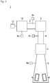
- the ion implantation apparatus 1 of the present example includes an ion source 10, which will be later described, a travel chamber 2, a mass spectrometer 3, an accelerator 4, a scanning device 5, and an implantation chamber 6, which are connected in this order.
- the ion implantation apparatus 1 is configured so that the ion source 10, the travel chamber 2, the accelerator 4, and the implantation chamber 6 are evacuated by evacuation devices 9a to 9d, respectively.
- the ion source 10 is connected with a gas supply unit 12 and generates an ion by using a gas supplied from the gas supply unit 12, and a positively-charged ion is extracted in the travel chamber 2, travels within the travel chamber 2, and then enters into the mass spectrometer 3.
- an aluminum ion passes and enters into the accelerator 4.
- the aluminum ion which has entered into the accelerator 4 is accelerated and, when it enters into the scanning device 5,the resulting ion beam is controlled by the scanning device 5 with respect to a direction of travel of the ion beam, and the ion beam enters into the implantation chamber 6.
- the chamber 21 includes two bottom surfaces 31 and 32.
- One bottom surface 31 is located in one end of the chamber 21 while the other bottom surface 32 is located in the other end of the chamber 21, and the bottom surfaces 31 and 32 are provided with mounting holes 47 and 48, respectively.
- a filament 20 is arranged in a position close to the one bottom surface 31, and a repeller electrode 23 is placed in a position close to the other bottom surface 32.
- the filament 20 is arranged in the vacuum environment outside the chamber 21.
- a cathode electrode 22 is arranged in a position close to the filament 20. Accordingly, the cathode electrode 22 is arranged on a side where the one bottom surface is provided, and the repeller electrode 23 is placed on a side where the other bottom surface is provided.
- Each of the cathode electrode 22 and the repeller electrode 23 has a shape of a flat plate or a column, respective surfaces which face each other are made parallel to each other, and the filament 20 is arranged on a back side of the cathode electrode 22.
- a base plate 30 is arranged near the bottom surface 31 close to the filament 20.
- the base plate 30 is fixed to the chamber 21 in a state of being insulated.
- a raw-material supporting unit 26 and an electrode supporting unit 33 are inserted through the mounting hole 47 of the bottom surface 31 close to the filament 20, then a tip end of the electrode supporting unit 33 which is one end of the electrode supporting unit 33 is placed within the chamber 21, and a base portion of the electrode supporting unit 33 which is the other end of the electrode supporting unit 33 is fixed to the base plate 30.
- the cathode electrode 22 is mounted onto the tip end of the electrode supporting unit 33 by a structure not shown in the drawings. It is noted that the electrode supporting unit 33 and the cathode electrode 22 may be incorporated into an integral structure.
- the supporting rod 36 has electrical conductivity, and a portion of the supporting rod 36, whose portion is on a side opposite to a tip end, is arranged outside the chamber 21.
- the supporting rod 36 is fixed to the chamber 21 by an insulator 41, and the supporting rod 36 and the chamber 21 are insulated from each other.
- the raw-material supporting unit 26 is arranged between an edge of the mounting hole 47 and the electrode supporting unit 33 while being out of contact with the chamber 21 and the electrode supporting unit 33.
- a base of the raw-material supporting unit 26 is fixed to the base plate 30, and a raw-material block 28 formed of a solid aluminum compound which is molded into a predetermined shape is attached to a tip end of the raw-material supporting unit 26.
- an aluminum compound is aluminum nitride (AlN).
- the raw-material block 28 is arranged between a side surface of the cathode electrode 22 and a side surface 25 of the chamber 21 while being out of contact with both of the cathode electrode 22 and the chamber 21, and an evaporation surface 37 which is one surface out of surfaces of a plurality of the raw-material block 28.
- the one surface facing the repeller electrode 23, which is spaced from the raw-material block 28, is made flat and is made parallel to respective surfaces of the cathode electrode 22 and the repeller electrode 23 which are made parallel to each other.
- a flat surface where the evaporation surface 37 is included is located between a surface of the repeller electrode 23, i.e., the surface facing the cathode electrode 22, and the electron emitting surface 38.
- the evaporation surface 37 is arranged in such a position so as to make a distance between a flat surface where the evaporation surface is included and the repeller electrode 23 smaller than a distance between the electron emitting surface 38 and the repeller electrode 23.
- the evaporation surface 37 is arranged in such a position so as to make a distance between a flat surface where the evaporation surface 37 is included and the electron emitting surface 38 smaller than a distance between a flat surface where the evaporation surface 37 is included and the repeller electrode 23.
- Fig. 4(a) is a plan view of the raw-material block 28.
- the raw-material block 28 has a ring shape with a window hole 27 formed in a center of a metal body, and the electron emitting surface 38 of the cathode electrode 22 is arranged in the window hole 27 formed in the center, so that the emitting surface 38 is exposed in the window hole 27.
- the window hole 27 has a circular shape
- the cathode electrode 22 has a shape of a disk
- the design is such that a diameter of the window hole 27 is larger than a diameter of the cathode electrode 22.
- a discharge power supply 52, a cathode-heating power supply 53, and a filament-heating power supply 54 are arranged outside the chamber 21.
- Apositive-voltage terminal of the discharge power supply 52 is electrically connected to the chamber 21.
- Anegative-voltage terminal of the discharge power supply 52 is electrically connected to the base plate 30.
- electrical connection is established via the raw-material supporting unit 26. Accordingly, when the discharge power supply 52 operates, a negative voltage with respect to the chamber 21 is applied to each of the cathode electrode 22 and the raw-material block 28.
- a negative-voltage terminal of the discharge power supply 52 is electrically connected to a positive-voltage terminal of the cathode-heating power supply 53, and a negative-voltage terminal of the cathode-heating power supply 53 is electrically connected to one end of the filament 20.
- a negative voltage with respect to the cathode electrode 22 is applied to the filament 20.
- one end of the filament 20 is electrically connected to a negative-voltage terminal of the cathode-heating power supply 53 and a negative-voltage terminal of the filament-heating power supply 54, and the other end of the filament 20 is electrically connected to a positive-voltage terminal of the filament-heating power supply 54.
- the cathode electrode 22, the repeller electrode 23, and the filament 20 are arranged in a vacuum environment, and heat is generated when the filament-heating power supply 54 operates and a current is flowing through the filament 20 in the vacuum environment.
- thermoelectron is emitted from the filament 20 toward the cathode electrode 22, and when the thermoelectron collides with the cathode electrode 22, the cathode electrode 22 is heated.
- thermoelectron is emitted from the exposed electron emitting surface 38 of the cathode electrode 22 toward the repeller electrode 23, and is accelerated.
- thermoelectron which is emitted from the cathode electrode 22 and is accelerated (this thermoelectron will hereinafter be referred to as a primary electron) flies toward the cathode electrode 22 as a direction of flight thereof is reversed by electrostatic force.
- the primary electron which travels toward the cathode electrode 22 is reversed toward the repeller electrode 23 as a direction of flight thereof is reversed by the cathode electrode 22.
- a magnet 58 in which one of two magnetic poles of the north pole and the south pole is directed toward the chamber 21, and a magnet 59 in which the other pole is directed toward the chamber 21, are arranged, and magnetic lines formed between the north pole and the south pole are designed so as to penetrate the cathode electrode 22 and the repeller electrode 23.
- the primary electron reciprocally moves while spirally moving by winding around magnetic lines.
- a gas introduction hole 34 and an ion emission hole 35 are provided.
- the gas introduction hole 34 is connected to the gas supply unit 12, and when a fluorine-compound gas is supplied from the gas supply unit 12, a fluorine-compound gas is decomposed by the primary electron which reciprocally moves in the chamber 21, so that a fluorine ion or a fluorine radical is generated.
- the cathode electrode 22 is formed of high-melting-point metal, and is heated to a temperature of about 2200 °C by the filament 20.
- the raw-material block 28 is arranged near the cathode electrode 22 while being out of contact with the cathode electrode 22, and the raw-material block 28 is arranged while being out of contact with the chamber 21.
- the raw-material block 28 is heated by heat rays emitted from the cathode electrode 22 in order not to flow out heat to chamber 21, and a temperature is increased.
- the evaporation surface 37 facing the repeller electrode 23, which is spaced from the raw-material block 28, is arranged in a position which is closer to the repeller electrode 23 than the electron emitting surface 38, and the raw-material block 28 is configured such that the raw-material block 28 is heated to a temperature in a range of 1200 °C to 1700 °C by means of adjusting a temperature of the cathode electrode 22, and adjusting a distance between the evaporation surface 37 of the raw-material block 28, the evaporation surface 37 being facing the repeller electrode 23, and the electron emitting surface 38.
- the distance is in a direction perpendicular to the electron emitting surface 38, a distance between the raw-material block 28 and a side surface of the cathode electrode 22, and a distance between the raw-material block 28 and an inner side surface of the chamber 21.
- Plasma containing a fluorine ion or a fluorine radical is generated from a fluorine-compound gas introduced into the chamber 21 by the primary electron, and the evaporation surface 37 comes into contact with generated plasma.
- Plasma comes into contact with aluminum nitride exposed in the evaporation surface 37, and aluminum nitride reacts with fluorine such as a fluorine ion or a fluorine radical in plasma, so that aluminum fluoride (AlF x ) is generated.
- Aluminum fluoride changes to a gas by being heated to a high temperature, and is emitted to the inside of the chamber 21 from the raw-material block 28. Since aluminum fluoride gas is generated in the heated chamber 21, aluminum fluoride does not precipitate in an inside of the pipe connected with the chamber 21.
- Aluminum fluoride which is emitted is decomposed by the primary electron reciprocally moving in the chamber 21, so that an aluminum ion (Al + ) is generated.
- the aluminum ion is included among the positively-charged ions which enter into the travel chamber 2.
- a phosphorus-trifluoride (PF 3 ) gas or a boron-trifluoride (BF 3 ) gas can be used.
- PF 3 phosphorus-trifluoride
- BF 3 boron-trifluoride
- boron nitride (BN) which has a high evaporation temperature, is generated as a byproduct, and boron nitride is accumulated in the chamber 21.
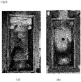
- Fig. 6(a) is a photograph showing a state of byproducts in the chamber 21 in a case where a boron-trifluoride gas is used
- Fig. 6(b) is a photograph showing a state of byproducts in the chamber 21 in a case where a phosphorus-trifluoride gas is used.
- An amount of byproducts in the case where a phosphorus-trifluoride gas is used is relatively small.
- an aluminum ion can be generated by using a nitrogen-trifluoride (NF 3 ) gas
- NF 3 nitrogen-trifluoride
- the raw-material block 28 shouldbe heated to a temperature equal to or higher than 1200 °C at a minimum in order to emit a necessary amount of aluminum fluoride.
- a higher heating temperature is desirable, but nitrogen gas is also emitted together with emission of aluminum fluoride.
- Fig. 5 is a graph showing a relationship between a temperature of aluminum nitride and a partial pressure of a nitrogen gas (N 2 ) emitted from aluminum nitride (see, " Shinku", Vol. 9 (1966) , No. 5, pp. 183-189 ) , and the graph indicates that an upper limit of a temperature of aluminum nitride is equal to 1700 °C because an upper limit of an operating pressure of an ion source is equal to approximately 5 ⁇ 10 -3 mmHg.
- N 2 nitrogen gas
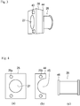
- Fig. 3 is a perspective view for explaining one example in which the raw-material block 28 is attached to the raw-material supporting unit 26, and Fig. 4 (c) is a side view of the raw-material supporting unit 26.
- Each of the electrode supporting unit 33 and the raw-material supporting unit 26 is a hollow cylinder in this example, and it is designed such that a diameter of the electrode supporting unit 33 is smaller than a diameter of the raw-material supporting unit 26 in this example.
- the electrode supporting unit 33 and the raw-material supporting unit 26 are fixed to the base plate 30 with coinciding center axis lines and with the electrode supporting unit 33 being arranged in a hollow inner portion of the raw-material supporting unit 26.
- a protruding portion 46 is provided in a tip end of the raw-material supporting unit 26.
- the protruding portion 46 protrudes in an outward direction perpendicular to a side surface of the raw-material supporting unit 26, and can be formed in a shape of a flange, for example.
- the protruding portion 46, an attaching member 44 and a screw 43, which will be later described, and the like are omitted.
- the attaching member 44 has a semicircular attaching hole 45 formed therein.
- the attaching hole 45 is formed such that a diameter of a semicircular shape thereof is equal to, or a little larger than, an outside diameter of the raw-material supporting unit 26. Accordingly, the attaching member 44 can be fitted to the raw-material supporting unit 26 so that the raw-material supporting unit 26 is located in the attaching hole 45.
- the repeller electrode 23 is placed in a lower position in the chamber 21, the raw-material supporting unit 26 is arranged vertically so that the protruding portion 46 is located in a lower end of the raw-material supporting unit 26, and the raw-material supporting unit 26 is fixed to the chamber 21 in a state that electric insulation is kept between the raw-material supporting unit 26 and the chamber 21.
- the attaching member 44 When the attaching member 44 is mounted on the raw-material supporting unit 26, the attaching member 44 is placed on the protruding portion 46.
- An insertion hole 29a into which a screw can be inserted is formed in the raw-material block 28, and a screw hole 29b which has a screw groove formed in an inner surface thereof is provided in the attaching member 44.
- the raw-material block 28 is brought into contact with a surface of the protruding portion 46, i.e., the surface facing the repeller electrode 23,while the protruding portion 46 is held between the raw-material block 28 and the attaching member 44.
- a screw 43 is inserted into the insertion hole 29a of the raw-material block 28, as shown in Fig. 3 , and a tip end of the screw 43 is screwed into the screw hole 29b of the attaching member 44.
- the screw 43 is rotated to apply force in such a direction so as to bring the raw-material block 28 and the attaching member 44 close to each other, such that a screw head of the screw 43 is brought into contact with the raw-material block 28,the protruding portion 46 is pinched between the raw-material block 28 and the attaching member 44, and the raw-material block 28 is fixed to the raw-material supporting unit 26.
- the raw-material block 28 does not need to be pressed against the attaching member 44 by a thrust of the screw 43.
- a surface pressure being pinched may be reduced because of consumption of the raw-material block 28, in some cases, even though the raw-material block 28 is fixed by a thrust of the screw 43. Nonetheless, under circumstances where an ion implantation apparatus is vibrating, a screw does not voluntarily rotate, so that a distance which is given at a time of initial fastening is kept unchanged. Accordingly, even if a portion of the raw-material block 28, the portion coming into contact with a flange of the screw 43, is consumed, an angle at which the protruding portion 46 is pinched is only slightly increased by weights of the raw-material block 28 and the attaching member 44, and the raw-material block 28 is prevented from dropping off.
- small fastening torque may be given to the screw 43 which is provided in order to pinch the protruding portion 46.
- small fastening torque facilitates an operation for attaching the raw-material block 28.
- each of the attaching member 44 and the screw 43 is configured by a process in which a stainless-steel material is molded.
- "galling" which is an adhering phenomenon occurs.
- fastening torque is small in the present invention, so that "galling” does not occur and a probability of a problem occurring at a time of detachment is reduced. Also, a dry lubricant becomes unnecessary.
Landscapes
- Chemical & Material Sciences (AREA)
- Analytical Chemistry (AREA)
- Engineering & Computer Science (AREA)
- Chemical Kinetics & Catalysis (AREA)
- Materials Engineering (AREA)
- Mechanical Engineering (AREA)
- Metallurgy (AREA)
- Organic Chemistry (AREA)
- Combustion & Propulsion (AREA)
- Electron Sources, Ion Sources (AREA)
- Plasma Technology (AREA)
Abstract
Description
- The present invention relates to an ion source, and particularly to a technique regarding an ion source used for an ion implantation apparatus.
- In recent years, a method for manufacturing a substrate of silicon carbide (SiC) that has better heat resistance and can better withstand voltage compared to an existing silicon (Si) substrate has been established, thereby making SiC substrates available at a relatively low cost.
- A process using an SiC substrate includes a process of implanting an aluminum ion as a dopant, and an ion implantation apparatus that includes an ion source for generating an aluminum ion beam.
- In the ion source as described above, as methods for generating an aluminum ion, there is a method in which aluminum chloride is heated to generate an aluminum ion. However, this method has low productivity. As such, , another method in which aluminum nitride and a fluorine-based gas are reacted with each other to generate the aluminum ion have been adopted.
- However, even with the method in which aluminum nitride and a fluorine-based gas react with each other, there are problems in that aluminum fluoride (AlFx) is generated as an intermediate product, the generated aluminum fluoride is deposited within a reaction chamber, and generation of the aluminum ion is suspended.
- For those reasons, conventional techniques suffer from a problem of a need for frequent maintenance of an ion source.
-
- Patent Literature 1:
JP 3325393 B2 - Patent Literature 2:
JP 4428467 B2 - It is an object of the present invention to provide a technique which allows for generation of an aluminum ion without deposition of an intermediate product in a reaction chamber.
- To solve the above-described problems associated with the conventional technique, the present embodiment provides an ion source comprising a cathode electrode arranged in one end of an inside of a chamber, a repeller electrode arranged in the other end of the inside of the chamber and facing a surface of the cathode electrode, a filament arranged on a back-surface side of the cathode electrode, a gas introduction hole to which a fluorine-compound gas is introduced, the gas introduction hole being provided in the chamber, and an emission hole through which a positively-charged ion is extracted out of the chamber, wherein a raw-material block is arranged in the chamber, the cathode electrode is heated by the filament through which a current is flowing, and a thermoelectron is emitted from an electron emitting surface of the surface of the cathode electrode toward the repeller electrode, the thermoelectron decomposing the fluorine-compound gas introduced through the gas introduction hole and generating plasma by reciprocally moving between the cathode electrode and the repeller electrode, and the positively-charged aluminum ion is generated by reaction of fluorine in the plasma with the raw-material block, the raw-material block is arranged near a side surface of the cathode electrode while being out of contact with the cathode electrode and the chamber, the raw-material block is aluminum nitride, the fluorine-compound gas is a phosphorus-trifluoride gas, and aluminum fluoride that is generated from the raw-material block and the fluorine-compound gas is decomposed by the thermoelectron so that an aluminum ion that is to be extracted out of the chamber is generated.
- Also, the present embodiment provides the ion source, wherein the fluorine-compound gas is converted into the plasma by the thermoelectron, and an evaporation surface of the raw-material block, which is facing the repeller electrode and contacts the plasma, is located between a surface of the repeller electrode which is facing the cathode electrode and the electron emitting surface, and is located in such a position that a distance between a flat surface in which the evaporation surface is included and the electron emitting surface is smaller than a distance between the flat surface that includes the evaporation surface and a surface of the repeller electrode, the surface of the repeller electrode facing the electron emitting surface.
- Also, the present embodiment provides the ion source, wherein the raw-material block is heated to a temperature in a range of 1200 °C to 1700 °C, by heat generation of the cathode electrode.
- Also, the present embodiment provides the ion source, wherein the raw-material block is arranged in a tip end of a raw-material supporting unit, a protruding portion that protrudes in an outward direction that is perpendicular to a side surface of the raw-material supporting unit is provided in the tip end of the raw-material supporting unit, the raw-material block is arranged on a surface of the protruding portion, the surface of the protruding portion facing the repeller electrode, and an attaching member is arranged on a back surface, and the raw-material block and the attaching member are pressed against with each other with a screw, and the protruding portion is pinched between the raw-material block and the attaching member so that the raw-material block is fixed to the raw-material supporting unit.
- The present embodiment provides an ion implantation apparatus comprising an ion source, wherein the ion source includes a cathode electrode arranged in one end of an inside of a chamber, a repeller electrode arranged in the other end of the inside of the chamber and facing a surface of the cathode electrode, a filament arranged on a back-surface side of the cathode electrode, a gas introduction hole to which a fluorine-compound gas is introduced, the gas introduction hole being provided in the chamber, and an emission hole through which a positively-charged ion is extracted out of the chamber, wherein a raw-material block is arranged in the chamber, the cathode electrode is heated by the filament through which a current is flowing, and a thermoelectron is emitted from an electron emitting surface of the surface of the cathode electrode toward the repeller electrode, the thermoelectron decomposing the fluorine compound gas introduced through the gas introduction hole and generating plasma by reciprocally moving between the cathode electrode and the repeller electrode, and the positively-charged aluminum ion is generated by reaction of fluorine in the plasma with the raw-material block, the raw-material block is arranged near a side surface of the cathode electrode while being out of contact with the cathode electrode and the chamber, the raw-material block is aluminum nitride, the fluorine-compound gas is a phosphorus-trifluoride gas, and aluminum fluoride that is generated from the raw-material block and the fluorine-compound gas is decomposed by the thermoelectron so that an aluminum ion that is to be extracted out of the chamber is generated, the ion implantation apparatus further comprising; an extraction electrode arranged adjacent to the emission hole, the extraction electrode being configured to extract the positively-charged ion in the chamber, a mass spectrometer configured to mass-analyze the ion extracted by the extraction electrode, and an implantation chamber in which a substrate being irradiated with the ion that is mass-analyzed is arranged.
- The present embodiment provides the ion implantation apparatus, wherein the fluorine-compound gas is converted into the plasma by the thermoelectron, and an evaporation surface of the raw-material block, which is facing the repeller electrode and contacts the plasma, is located between a surface of the repeller electrode which is facing the cathode electrode and the electron emitting surface, and is located in a such a position that a distance between a flat surface that includes the evaporation surface and the electron emitting surface is smaller than a distance between the flat surface in which the evaporation surface is included and a surface of the repeller electrode, the surface of the repeller electrode facing the electron emitting surface.
- Further, the present embodiment provides the ion implantation apparatus, wherein the raw-material block is heated to a temperature in a range of 1200 °C to 1700 °C, by heat generation of the cathode electrode.
- The present embodiment provides the ion implantation apparatus, wherein the raw-material block in the ion source is arranged in a tip end of a raw-material supporting unit, a protruding portion that protrudes in an outward direction that is perpendicular to a side surface of the raw-material supporting unit is provided in the tip end of the raw-material supporting unit, the raw-material block is arranged on a surface of the protruding portion, the surface of the protruding portion facing the repeller electrode, and an attaching member is arranged on a back surface, and the raw-material block and the attaching member are pressed against with each other with a screw, and the protruding portion is pinched between the raw-material block and the attaching member so that the raw-material block is fixed to the raw-material supporting unit.
- According to the present invention, a long-lasting and durable ion source that can generate a large amount of aluminum ions, and an ion implantation apparatus which includes the foregoing ion source, can be provided. Also, aluminum ions can be implanted stably for a long time.
- It is easy to replace the raw-material block.
-
-
Fig. 1 is a schematic configuration diagram showing a whole of one example of an ion implantation apparatus according to the present invention using an ion source according to the present invention. -
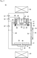
Fig. 2 is a sectional view showing an example of a configuration of the ion source according to the present invention. -
Fig. 3 is a view for explaining a positional relationship between a raw-material block and a raw-material supporting unit. -
Fig. 4 (a) is a plan view of the raw-material block,Fig. 4(b) is a plan view of an attaching member, andFig. 4(c) is a side view of the raw-material supporting unit. -
Fig. 5 is a graph showing a relationship between a temperature of aluminum nitride and a partial pressure of a nitrogen gas (N2) being emitted. -
Fig. 6 includes photographs each showing a state in which byproducts are accumulated within a chamber, andFig. 6 (a) shows a case where a boron-trifluoride gas is used whileFig. 6(b) shows a case where a phosphorus-trifluoride is used. - Hereinbelow, an embodiment of the present invention will be described with reference to the drawings.
-
Fig. 1 is a schematic configuration diagram showing a whole of anion implantation apparatus 1 according to the present invention using an ion source according to the present invention. - As shown in
Fig. 1 , theion implantation apparatus 1 of the present example includes anion source 10, which will be later described, atravel chamber 2, amass spectrometer 3, anaccelerator 4, a scanning device 5, and animplantation chamber 6, which are connected in this order. - It is noted that the
ion implantation apparatus 1 is configured so that theion source 10, thetravel chamber 2, theaccelerator 4, and theimplantation chamber 6 are evacuated byevacuation devices 9a to 9d, respectively. - The
ion source 10 is connected with agas supply unit 12 and generates an ion by using a gas supplied from thegas supply unit 12, and a positively-charged ion is extracted in thetravel chamber 2, travels within thetravel chamber 2, and then enters into themass spectrometer 3. - A positively-charged ion is mass-analyzed while it is passing through the inside of the
mass spectrometer 3, and an ion having a desired mass-to-charge ratio passes through themass spectrometer 3 and enters into theaccelerator 4. - Here, an aluminum ion passes and enters into the
accelerator 4. - In the
accelerator 4, the aluminum ion which has entered into theaccelerator 4 is accelerated and, when it enters into the scanning device 5,the resulting ion beam is controlled by the scanning device 5 with respect to a direction of travel of the ion beam, and the ion beam enters into theimplantation chamber 6. - A plurality of (two in this example)
substrates 8 are arranged in theimplantation chamber 6. The ion beam is directed toward a certain substrate out of the plurality ofsubstrates 8 by the above-described scanning device 5 and is irradiated on a surface of the certain substrate. A surface of thesubstrate 8 is scanned by an ion beam, and the ion is implanted. -
Fig. 2 is a view for explaining the inside of theion source 10 according to the present invention. In theion source 10, achamber 21 having a shape of a tube (a rectangular tube in this example) is arranged, and the inside of thechamber 21 is evacuated by theevacuation device 9a shown inFig. 1 to create a vacuum environment. - The
chamber 21 includes twobottom surfaces bottom surface 31 is located in one end of thechamber 21 while theother bottom surface 32 is located in the other end of thechamber 21, and thebottom surfaces mounting holes chamber 21, afilament 20 is arranged in a position close to the onebottom surface 31, and arepeller electrode 23 is placed in a position close to theother bottom surface 32. Thefilament 20 is arranged in the vacuum environment outside thechamber 21. - Inside the
chamber 21, between thefilament 20 and therepeller electrode 23, acathode electrode 22 is arranged in a position close to thefilament 20. Accordingly, thecathode electrode 22 is arranged on a side where the one bottom surface is provided, and therepeller electrode 23 is placed on a side where the other bottom surface is provided. Each of thecathode electrode 22 and therepeller electrode 23 has a shape of a flat plate or a column, respective surfaces which face each other are made parallel to each other, and thefilament 20 is arranged on a back side of thecathode electrode 22. - Outside of the
chamber 21, abase plate 30 is arranged near thebottom surface 31 close to thefilament 20. Thebase plate 30 is fixed to thechamber 21 in a state of being insulated. - A raw-
material supporting unit 26 and anelectrode supporting unit 33 are inserted through themounting hole 47 of thebottom surface 31 close to thefilament 20, then a tip end of theelectrode supporting unit 33 which is one end of theelectrode supporting unit 33 is placed within thechamber 21, and a base portion of theelectrode supporting unit 33 which is the other end of theelectrode supporting unit 33 is fixed to thebase plate 30. Thecathode electrode 22 is mounted onto the tip end of theelectrode supporting unit 33 by a structure not shown in the drawings. It is noted that theelectrode supporting unit 33 and thecathode electrode 22 may be incorporated into an integral structure. - A supporting
rod 36 is inserted into themounting hole 48 in thebottom surface 32 which is located relatively far from thefilament 20. A tip end of the supportingrod 36 is arranged within thechamber 21, and therepeller electrode 23 is fixed to the tip end of the supportingrod 36. - The supporting
rod 36 has electrical conductivity, and a portion of the supportingrod 36, whose portion is on a side opposite to a tip end, is arranged outside thechamber 21. - The supporting
rod 36 is fixed to thechamber 21 by aninsulator 41, and the supportingrod 36 and thechamber 21 are insulated from each other. - The raw-
material supporting unit 26 is arranged between an edge of the mountinghole 47 and theelectrode supporting unit 33 while being out of contact with thechamber 21 and theelectrode supporting unit 33. - A base of the raw-
material supporting unit 26 is fixed to thebase plate 30, and a raw-material block 28 formed of a solid aluminum compound which is molded into a predetermined shape is attached to a tip end of the raw-material supporting unit 26. In this example, an aluminum compound is aluminum nitride (AlN). - The
electrode supporting unit 33 and the raw-material supporting unit 26 have electrical conductivity and are at the same potential as thebase plate 30, so that thecathode electrode 22 and the raw-material block 28 are also at the same potential as thebase plate 30. - The raw-
material block 28 is arranged between a side surface of thecathode electrode 22 and aside surface 25 of thechamber 21 while being out of contact with both of thecathode electrode 22 and thechamber 21, and anevaporation surface 37 which is one surface out of surfaces of a plurality of the raw-material block 28. The one surface facing therepeller electrode 23, which is spaced from the raw-material block 28, is made flat and is made parallel to respective surfaces of thecathode electrode 22 and therepeller electrode 23 which are made parallel to each other. - Assuming that a surface of the
cathode electrode 22, i.e., the surface facing therepeller electrode 23, is referred to as anelectron emitting surface 38, a flat surface where theevaporation surface 37 is included is located between a surface of therepeller electrode 23, i.e., the surface facing thecathode electrode 22, and theelectron emitting surface 38. In other words, theevaporation surface 37 is arranged in such a position so as to make a distance between a flat surface where the evaporation surface is included and therepeller electrode 23 smaller than a distance between theelectron emitting surface 38 and therepeller electrode 23. Also, theevaporation surface 37 is arranged in such a position so as to make a distance between a flat surface where theevaporation surface 37 is included and theelectron emitting surface 38 smaller than a distance between a flat surface where theevaporation surface 37 is included and therepeller electrode 23. -
Fig. 4(a) is a plan view of the raw-material block 28. As shown inFig. 4 (a) , the raw-material block 28 has a ring shape with awindow hole 27 formed in a center of a metal body, and theelectron emitting surface 38 of thecathode electrode 22 is arranged in thewindow hole 27 formed in the center, so that the emittingsurface 38 is exposed in thewindow hole 27. - In the present example, the
window hole 27 has a circular shape, thecathode electrode 22 has a shape of a disk, and the design is such that a diameter of thewindow hole 27 is larger than a diameter of thecathode electrode 22. - A
discharge power supply 52, a cathode-heating power supply 53, and a filament-heating power supply 54 are arranged outside thechamber 21. - Apositive-voltage terminal of the
discharge power supply 52 is electrically connected to thechamber 21. - Anegative-voltage terminal of the
discharge power supply 52 is electrically connected to thebase plate 30. Here, electrical connection is established via the raw-material supporting unit 26. Accordingly, when thedischarge power supply 52 operates, a negative voltage with respect to thechamber 21 is applied to each of thecathode electrode 22 and the raw-material block 28. - Also, a negative-voltage terminal of the
discharge power supply 52 is electrically connected to a positive-voltage terminal of the cathode-heating power supply 53, and a negative-voltage terminal of the cathode-heating power supply 53 is electrically connected to one end of thefilament 20. When the cathode-heating power supply 53 operates, a negative voltage with respect to thecathode electrode 22 is applied to thefilament 20. - Also, one end of the
filament 20 is electrically connected to a negative-voltage terminal of the cathode-heating power supply 53 and a negative-voltage terminal of the filament-heating power supply 54, and the other end of thefilament 20 is electrically connected to a positive-voltage terminal of the filament-heating power supply 54. - The
cathode electrode 22, therepeller electrode 23, and thefilament 20 are arranged in a vacuum environment, and heat is generated when the filament-heating power supply 54 operates and a current is flowing through thefilament 20 in the vacuum environment. - In the foregoing state, while a negative voltage with respect to the
cathode electrode 22 is being applied to thefilament 20 by the cathode-heating power supply 53, a thermoelectron is emitted from thefilament 20 toward thecathode electrode 22, and when the thermoelectron collides with thecathode electrode 22, thecathode electrode 22 is heated. - In a state where a negative voltage with respect to the
chamber 21 is being applied to thecathode electrode 22 by thedischarge power supply 52, when thecathode electrode 22 is heated, a thermoelectron is emitted from the exposedelectron emitting surface 38 of thecathode electrode 22 toward therepeller electrode 23, and is accelerated. - The
repeller electrode 23, which is at a floating potential, is at the same negative potential as thecathode electrode 22, and a thermoelectron which is emitted from thecathode electrode 22 and is accelerated (this thermoelectron will hereinafter be referred to as a primary electron) flies toward thecathode electrode 22 as a direction of flight thereof is reversed by electrostatic force. - Also, the primary electron which travels toward the
cathode electrode 22 is reversed toward therepeller electrode 23 as a direction of flight thereof is reversed by thecathode electrode 22. - In the above-described manner, a primary electron reciprocally moves between the
cathode electrode 22 and therepeller electrode 23. - Outside the
chamber 21, amagnet 58 in which one of two magnetic poles of the north pole and the south pole is directed toward thechamber 21, and amagnet 59 in which the other pole is directed toward thechamber 21, are arranged, and magnetic lines formed between the north pole and the south pole are designed so as to penetrate thecathode electrode 22 and therepeller electrode 23. - Accordingly, the primary electron reciprocally moves while spirally moving by winding around magnetic lines. By the above-described actions, the probability of collision between a gas and an electron in the
chamber 21 is increased in an attempt to increase an efficiency of producing plasma. - In a side surface of the
chamber 21, agas introduction hole 34 and anion emission hole 35 are provided. - The
gas introduction hole 34 is connected to thegas supply unit 12, and when a fluorine-compound gas is supplied from thegas supply unit 12, a fluorine-compound gas is decomposed by the primary electron which reciprocally moves in thechamber 21, so that a fluorine ion or a fluorine radical is generated. - The
cathode electrode 22 is formed of high-melting-point metal, and is heated to a temperature of about 2200 °C by thefilament 20. - The raw-
material block 28 is arranged near thecathode electrode 22 while being out of contact with thecathode electrode 22, and the raw-material block 28 is arranged while being out of contact with thechamber 21. - Accordingly, the raw-
material block 28 is heated by heat rays emitted from thecathode electrode 22 in order not to flow out heat tochamber 21, and a temperature is increased. - As described above, among surfaces of the raw-
material block 28, theevaporation surface 37 facing therepeller electrode 23, which is spaced from the raw-material block 28, is arranged in a position which is closer to therepeller electrode 23 than theelectron emitting surface 38, and the raw-material block 28 is configured such that the raw-material block 28 is heated to a temperature in a range of 1200 °C to 1700 °C by means of adjusting a temperature of thecathode electrode 22, and adjusting a distance between theevaporation surface 37 of the raw-material block 28, theevaporation surface 37 being facing therepeller electrode 23, and theelectron emitting surface 38. The distance is in a direction perpendicular to theelectron emitting surface 38, a distance between the raw-material block 28 and a side surface of thecathode electrode 22, and a distance between the raw-material block 28 and an inner side surface of thechamber 21. - Plasma containing a fluorine ion or a fluorine radical is generated from a fluorine-compound gas introduced into the
chamber 21 by the primary electron, and theevaporation surface 37 comes into contact with generated plasma. Plasma comes into contact with aluminum nitride exposed in theevaporation surface 37, and aluminum nitride reacts with fluorine such as a fluorine ion or a fluorine radical in plasma, so that aluminum fluoride (AlFx) is generated. - Aluminum fluoride changes to a gas by being heated to a high temperature, and is emitted to the inside of the
chamber 21 from the raw-material block 28. Since aluminum fluoride gas is generated in theheated chamber 21, aluminum fluoride does not precipitate in an inside of the pipe connected with thechamber 21. - Aluminum fluoride which is emitted is decomposed by the primary electron reciprocally moving in the
chamber 21, so that an aluminum ion (Al+) is generated. - An
extraction electrode 24 shaped like a plate, to which a negative voltage with respect to thechamber 21 is applied, is placed in a position that is close to theion emission hole 35 and that is outside thechamber 21, and a positively-charged ion generated in thechamber 21 is attracted toward theextraction electrode 24 by an electric field formed by theextraction electrode 24, is extracted out of thechamber 21 through theion emission hole 35, and enters into the above-describedtravel chamber 2, passing through ahole 39 in the center of theextraction electrode 24. The aluminum ion is included among the positively-charged ions which enter into thetravel chamber 2. - As the above-described fluorine-compound gas, a phosphorus-trifluoride (PF3) gas or a boron-trifluoride (BF3) gas can be used. In a case where a boron-trifluoride gas is used, boron nitride (BN), which has a high evaporation temperature, is generated as a byproduct, and boron nitride is accumulated in the
chamber 21. -
Fig. 6(a) is a photograph showing a state of byproducts in thechamber 21 in a case where a boron-trifluoride gas is used, andFig. 6(b) is a photograph showing a state of byproducts in thechamber 21 in a case where a phosphorus-trifluoride gas is used. An amount of byproducts in the case where a phosphorus-trifluoride gas is used is relatively small. - While an aluminum ion can be generated by using a nitrogen-trifluoride (NF3) gas, it is more advantageous to use a phosphorus-trifluoride gas because a nitrogen-trifluoride gas is lower in reactivity than a phosphorus-trifluoride gas.
- In a case where alumina (Al2O3) is used for the raw-
material block 28, production of aluminum ions is small. Moreover, it is more advantageous to use aluminum nitride in that no oxygen plasma is generated. - When alumina and a BF3 gas are reacted with each other, a BO ion, which has the same mass-to-charge ratio as that of an aluminum ion, is generated, and thus, use of a combination of alumina and a BF3 gas is discouraged.
- The raw-
material block 28 shouldbe heated to a temperature equal to or higher than 1200 °C at a minimum in order to emit a necessary amount of aluminum fluoride. A higher heating temperature is desirable, but nitrogen gas is also emitted together with emission of aluminum fluoride. -
Fig. 5 is a graph showing a relationship between a temperature of aluminum nitride and a partial pressure of a nitrogen gas (N2) emitted from aluminum nitride (see, "Shinku", Vol. 9 (1966) , No. 5, pp. 183-189) , and the graph indicates that an upper limit of a temperature of aluminum nitride is equal to 1700 °C because an upper limit of an operating pressure of an ion source is equal to approximately 5 × 10⁻³ mmHg. -
Fig. 3 is a perspective view for explaining one example in which the raw-material block 28 is attached to the raw-material supporting unit 26, andFig. 4 (c) is a side view of the raw-material supporting unit 26. - Each of the
electrode supporting unit 33 and the raw-material supporting unit 26 is a hollow cylinder in this example, and it is designed such that a diameter of theelectrode supporting unit 33 is smaller than a diameter of the raw-material supporting unit 26 in this example. - The
electrode supporting unit 33 and the raw-material supporting unit 26 are fixed to thebase plate 30 with coinciding center axis lines and with theelectrode supporting unit 33 being arranged in a hollow inner portion of the raw-material supporting unit 26. - A protruding
portion 46 is provided in a tip end of the raw-material supporting unit 26. The protrudingportion 46 protrudes in an outward direction perpendicular to a side surface of the raw-material supporting unit 26, and can be formed in a shape of a flange, for example. InFig. 2 , the protrudingportion 46, an attachingmember 44 and ascrew 43, which will be later described, and the like are omitted. - As seen in
Fig. 4(b) the attachingmember 44 has a semicircular attachinghole 45 formed therein. The attachinghole 45 is formed such that a diameter of a semicircular shape thereof is equal to, or a little larger than, an outside diameter of the raw-material supporting unit 26. Accordingly, the attachingmember 44 can be fitted to the raw-material supporting unit 26 so that the raw-material supporting unit 26 is located in the attachinghole 45. - The
repeller electrode 23 is placed in a lower position in thechamber 21, the raw-material supporting unit 26 is arranged vertically so that the protrudingportion 46 is located in a lower end of the raw-material supporting unit 26, and the raw-material supporting unit 26 is fixed to thechamber 21 in a state that electric insulation is kept between the raw-material supporting unit 26 and thechamber 21. - When the attaching
member 44 is mounted on the raw-material supporting unit 26, the attachingmember 44 is placed on the protrudingportion 46. - An
insertion hole 29a into which a screw can be inserted is formed in the raw-material block 28, and ascrew hole 29b which has a screw groove formed in an inner surface thereof is provided in the attachingmember 44. - The raw-
material block 28 is brought into contact with a surface of the protrudingportion 46, i.e., the surface facing therepeller electrode 23,while the protrudingportion 46 is held between the raw-material block 28 and the attachingmember 44. Ascrew 43 is inserted into theinsertion hole 29a of the raw-material block 28, as shown inFig. 3 , and a tip end of thescrew 43 is screwed into thescrew hole 29b of the attachingmember 44. - Then, the
screw 43 is rotated to apply force in such a direction so as to bring the raw-material block 28 and the attachingmember 44 close to each other, such that a screw head of thescrew 43 is brought into contact with the raw-material block 28,the protrudingportion 46 is pinched between the raw-material block 28 and the attachingmember 44, and the raw-material block 28 is fixed to the raw-material supporting unit 26. At that time, because the raw-material block 28 is hung from the attachingmember 44 with thescrew 43, which is screwed and fixed to the attachingmember 44, and the raw-material block 28 is screwed and fixed to the attachingmember 44 with thescrew 43, to be prevented from dropping off the raw-material supporting unit 26, the raw-material block 28 does not need to be pressed against the attachingmember 44 by a thrust of thescrew 43. - As the raw-
material block 28 is consumed along with generation of ions, a surface pressure being pinched may be reduced because of consumption of the raw-material block 28, in some cases, even though the raw-material block 28 is fixed by a thrust of thescrew 43. Nonetheless, under circumstances where an ion implantation apparatus is vibrating, a screw does not voluntarily rotate, so that a distance which is given at a time of initial fastening is kept unchanged. Accordingly, even if a portion of the raw-material block 28, the portion coming into contact with a flange of thescrew 43, is consumed, an angle at which the protrudingportion 46 is pinched is only slightly increased by weights of the raw-material block 28 and the attachingmember 44, and the raw-material block 28 is prevented from dropping off. - For the above-described reasons, small fastening torque may be given to the
screw 43 which is provided in order to pinch the protrudingportion 46. - Small fastening torque results in suppression of thermal contact conduction between the raw-
material block 28 and the raw-material supporting unit 26, so that an amount of heat which flows from the raw-material block 28 is reduced. - Also, small fastening torque facilitates an operation for attaching the raw-
material block 28. - In the meantime, each of the attaching
member 44 and thescrew 43 is configured by a process in which a stainless-steel material is molded. When they are exposed to a high temperature environment under a state of large fastening torque, "galling" which is an adhering phenomenon occurs. However, fastening torque is small in the present invention, so that "galling" does not occur and a probability of a problem occurring at a time of detachment is reduced. Also, a dry lubricant becomes unnecessary. - Because of small fastening torque, by loosening the
screw 43, it is possible to easily detach the consumed raw-material block 28 from the raw-material supporting unit 26. After detachment, a new raw-material block 28 can be easily attached to the raw-material supporting unit 26. In this manner, it is easy to replace the raw-material block 28. -
- 1
- ION IMPLANTATION APPARATUS
- 10
- ION SOURCE
- 12
- GAS SUPPLY UNIT
- 20
- FILAMENT
- 21
- CHAMBER
- 22
- CATHODE ELECTRODE
- 23
- REPELLER ELECTRODE
- 26
- RAW-MATERIAL SUPPORTING UNIT
- 28
- RAW-MATERIAL BLOCK
- 38
- ELECTRON EMITTING SURFACE
Claims (8)
- An ion source (10) comprising:a cathode electrode (22) arranged in one end of an inside of a chamber (21);a repeller electrode (23) arranged in the other end of the inside of the chamber (21) and facing a surface of the cathode electrode (22);a filament (20) arranged on a back-surface side of the cathode electrode (22);a gas introduction hole (34) to which a fluorine-compound gas is introduced, the gas introduction hole (34) being provided in the chamber (21); andan emission hole (35) through which a positively-charged ion is extracted out of the chamber (21), whereina raw-material block (28) is arranged in the chamber (21),the cathode electrode (22) is heated by the filament (20) through which a current is flowing, and a thermoelectron is emitted from an electron emitting surface (38) of the surface of the cathode electrode (22) toward the repeller electrode (23), the thermoelectron decomposing the fluorine-compound gas introduced through the gas introduction hole (34) and generating plasma by reciprocally moving between the cathode electrode (22) and the repeller (23) electrode, and the positively-charged aluminum ion is generated by reaction of fluorine in the plasma with the raw-material block (28),the raw-material block (28) is arranged near a side surface of the cathode electrode (22) while being out of contact with the cathode electrode (22) and the chamber (21),the raw-material block (28) is aluminum nitride,the fluorine-compound gas is a phosphorus-trifluoride gas, andaluminum fluoride that is generated from the raw-material block (28) and the fluorine-compound gas is decomposed by the thermoelectron so that an aluminum ion that is to be extracted out of the chamber (21) is generated.
- The ion source (10) according to claim 1, wherein
the fluorine-compound gas is converted into the plasma by the thermoelectron, and
an evaporation surface (37) of the raw-material block (28), which is facing the repeller electrode (23) and contacts the plasma, is located between a surface of the repeller electrode (23) which is facing the cathode electrode (22) and the electron emitting surface (38), and is located in such a position that a distance between a flat surface in which the evaporation surface (37) is included and the electron emitting surface (38) is smaller than a distance between the flat surface that includes the evaporation surface (37) and a surface of the repeller electrode (23), the surface of the repeller electrode (23) facing the electron emitting surface (38). - The ion source (10) according to claim 1, wherein the raw-material block (28) is heated to a temperature in a range of 1200 °C to 1700 °C, by heat generation of the cathode electrode (22) .
- The ion source (10) according to claim 1, wherein
the raw-material block (28) is arranged in a tip end of a raw-material supporting unit (26),
a protruding portion (46) that protrudes in an outward direction that is perpendicular to a side surface of the raw-material supporting unit (26) is provided in the tip end of the raw-material supporting unit (26), the raw-material block (28) is arranged on a surface of the protruding portion (46), the surface of the protruding portion (46) facing the repeller electrode (23), and an attaching member (44) is arranged on a back surface, and
the raw-material block (28) and the attaching member (44) are pressed against with each other with a screw (43), and the protruding portion (46) is pinched between the raw-material block (28) and the attaching member (44) so that the raw-material block (28) is fixed to the raw-material supporting unit (26). - An ion implantation apparatus (1) comprising an ion source (10), wherein
the ion source (10) includes:a cathode electrode (22) arranged in one end of an inside of a chamber (21);a repeller electrode (23) arranged in the other end of the inside of the chamber (21) and facing a surface of the cathode electrode (22);a filament (20) arranged on a back-surface side of the cathode electrode (22);a gas introduction hole (34) to which a fluorine-compound gas is introduced, the gas introduction hole (34) being provided in the chamber (21); andan emission hole (35) through which a positively-charged ion is extracted out of the chamber (21), whereina raw-material block (28) is arranged in the chamber (21),the cathode electrode (22) is heated by the filament (20) through which a current is flowing, and a thermoelectron is emitted from an electron emitting surface (38) of the surface of the cathode electrode (22) toward the repeller electrode (23), the thermoelectron decomposing the fluorine-compound gas introduced through the gas introduction hole (34) and generating plasma by reciprocally moving between the cathode electrode (22) and the repeller electrode(23), and the positively-charged aluminum ion is generated by reaction of fluorine in the plasma with the raw-material block (28),the raw-material block (28) is arranged near a side surface of the cathode electrode (22) while being out of contact with the cathode electrode (22) and the chamber (21),the raw-material block (28) is aluminum nitride,the fluorine-compound gas is a phosphorus-trifluoride gas, andaluminum fluoride that is generated from the raw-material block (28) and the fluorine-compound gas is decomposed by the thermoelectron so that an aluminum ion that is to be extracted out of the chamber (21) is generated,the ion implantation apparatus (1) further comprising:an extraction electrode (24) arranged adjacent to the emission hole (35), the extraction electrode (24) being configured to extract the positively-charged ion in the chamber (21) ;a mass spectrometer (3) configured to mass-analyze the ion extracted by the extraction electrode (24); andan implantation chamber (6) in which a substrate (8) being irradiated with the ion that is mass-analyzed is arranged. - The ion implantation apparatus (1) according to claim 5, wherein
the fluorine-compound gas is converted into the plasma by the thermoelectron, and
an evaporation surface (37) of the raw-material block (28), which is facing the repeller electrode(23) and contacts the plasma, is located between a surface of the repeller electrode(23) which is facing the cathode electrode(22) and the electron emitting surface (38), and is located in a such a position that a distance between a flat surface that includes the evaporation surface (37) and the electron emitting surface (38) is smaller than a distance between the flat surface in which the evaporation surface (37) is included and a surface of the repeller electrode(23), the surface of the repeller electrode(23) facing the electron emitting surface (38). - The ion implantation apparatus (1) according to claim 5, wherein the raw-material block (28) is heated to a temperature in a range of 1200 °C to 1700 °C, by heat generation of the cathode electrode (22).
- The ion implantation apparatus (1) according to claim 5, wherein
the raw-material block (28) in the ion source (10) is arranged in a tip end of a raw-material supporting unit (26),
a protruding portion (46) that protrudes in an outward direction that is perpendicular to a side surface of the raw-material supporting unit (26) is provided in the tip end of the raw-material supporting unit (26), the raw-material block (28) is arranged on a surface of the protruding portion (46), the surface of the protruding portion (46) facing the repeller electrode (23), and an attaching member (44) is arranged on a back surface, and
the raw-material block (28) and the attaching member (44) are pressed against with each other with a screw (43), and the protruding portion (46) is pinched between the raw-material block (28) and the attaching member (44) so that the raw-material block (28) is fixed to the raw-material supporting unit (26).
Applications Claiming Priority (2)
| Application Number | Priority Date | Filing Date | Title |
|---|---|---|---|
| JP2017201641 | 2017-10-18 | ||
| PCT/JP2018/036195 WO2019077970A1 (en) | 2017-10-18 | 2018-09-28 | Ion source and ion injection device |
Publications (3)
| Publication Number | Publication Date |
|---|---|
| EP3699946A1 true EP3699946A1 (en) | 2020-08-26 |
| EP3699946A4 EP3699946A4 (en) | 2021-08-04 |
| EP3699946B1 EP3699946B1 (en) | 2024-10-09 |
Family
ID=66173682
Family Applications (1)
| Application Number | Title | Priority Date | Filing Date |
|---|---|---|---|
| EP18869340.2A Active EP3699946B1 (en) | 2017-10-18 | 2018-09-28 | Ion source and ion injection device |
Country Status (5)
| Country | Link |
|---|---|
| EP (1) | EP3699946B1 (en) |
| JP (1) | JP6514425B1 (en) |
| CN (1) | CN110100296B (en) |
| TW (1) | TWI687958B (en) |
| WO (1) | WO2019077970A1 (en) |
Cited By (2)
| Publication number | Priority date | Publication date | Assignee | Title |
|---|---|---|---|---|
| EP4411781A1 (en) * | 2023-02-03 | 2024-08-07 | II-VI Delaware, Inc. | Aluminum ion beam generation source |
| WO2025076203A1 (en) * | 2023-10-05 | 2025-04-10 | Axcelis Technologies, Inc. | Actively heated target to generate an ion beam |
Families Citing this family (4)
| Publication number | Priority date | Publication date | Assignee | Title |
|---|---|---|---|---|
| CN114242549B (en) * | 2021-12-21 | 2024-02-20 | 北京凯世通半导体有限公司 | An ion source device that uses material sputtering to form plasma |
| US11887806B2 (en) * | 2022-04-07 | 2024-01-30 | Applied Materials, Inc. | Composite ion source based upon heterogeneous metal-metal fluoride system |
| CN115241033A (en) * | 2022-07-25 | 2022-10-25 | 北京烁科中科信电子装备有限公司 | Indirectly heated solid metal ion source |
| CN116387147B (en) * | 2023-06-02 | 2023-08-29 | 合肥晶合集成电路股份有限公司 | Dielectric film, its manufacturing method and conductive plug |
Family Cites Families (11)
| Publication number | Priority date | Publication date | Assignee | Title |
|---|---|---|---|---|
| JPH06325711A (en) * | 1993-05-14 | 1994-11-25 | Ishikawajima Harima Heavy Ind Co Ltd | Sputter type ion source |
| EP0637052B1 (en) | 1993-07-29 | 1997-05-07 | Co.Ri.M.Me. Consorzio Per La Ricerca Sulla Microelettronica Nel Mezzogiorno | Method for producing a stream of ionic aluminum |
| GB0128913D0 (en) * | 2001-12-03 | 2002-01-23 | Applied Materials Inc | Improvements in ion sources for ion implantation apparatus |
| JP4646920B2 (en) * | 2003-12-12 | 2011-03-09 | セメクイップ, インコーポレイテッド | Method and apparatus for extending equipment operational time in ion implantation |
| JP4428467B1 (en) * | 2008-08-27 | 2010-03-10 | 日新イオン機器株式会社 | Ion source |
| JP5343835B2 (en) * | 2009-12-10 | 2013-11-13 | 日新イオン機器株式会社 | Reflective electrode structure and ion source |
| JP5925084B2 (en) | 2012-08-28 | 2016-05-25 | 住友重機械イオンテクノロジー株式会社 | Ion generation method and ion source |
| JP2015170451A (en) * | 2014-03-06 | 2015-09-28 | 日新イオン機器株式会社 | Ion source, and ion irradiation device using the same |
| JP6480222B2 (en) * | 2015-03-18 | 2019-03-06 | 株式会社アルバック | Ion beam apparatus, ion implantation apparatus, and ion beam emission method |
| CN104988335B (en) * | 2015-06-17 | 2018-02-09 | 昆明理工大学 | A kind of method for preparing metallic aluminium with alumina carbon tropical resources vacuum thermal decomposition |
| CN105448630A (en) * | 2015-12-11 | 2016-03-30 | 中国电子科技集团公司第四十八研究所 | Ion source for generating aluminum ion beam |
-
2018
- 2018-09-28 EP EP18869340.2A patent/EP3699946B1/en active Active
- 2018-09-28 WO PCT/JP2018/036195 patent/WO2019077970A1/en not_active Ceased
- 2018-09-28 JP JP2019506528A patent/JP6514425B1/en active Active
- 2018-09-28 CN CN201880005621.5A patent/CN110100296B/en active Active
- 2018-10-04 TW TW107135027A patent/TWI687958B/en active
Cited By (3)
| Publication number | Priority date | Publication date | Assignee | Title |
|---|---|---|---|---|
| EP4411781A1 (en) * | 2023-02-03 | 2024-08-07 | II-VI Delaware, Inc. | Aluminum ion beam generation source |
| US12586756B2 (en) | 2023-02-03 | 2026-03-24 | Ii-Vi Delaware, Inc. | Systems and methods for aluminum ion beam generation source technology |
| WO2025076203A1 (en) * | 2023-10-05 | 2025-04-10 | Axcelis Technologies, Inc. | Actively heated target to generate an ion beam |
Also Published As
| Publication number | Publication date |
|---|---|
| CN110100296A (en) | 2019-08-06 |
| TW201923809A (en) | 2019-06-16 |
| CN110100296B (en) | 2021-05-07 |
| JPWO2019077970A1 (en) | 2019-11-14 |
| EP3699946A4 (en) | 2021-08-04 |
| EP3699946B1 (en) | 2024-10-09 |
| WO2019077970A1 (en) | 2019-04-25 |
| TWI687958B (en) | 2020-03-11 |
| JP6514425B1 (en) | 2019-05-15 |
Similar Documents
| Publication | Publication Date | Title |
|---|---|---|
| EP3699946B1 (en) | Ion source and ion injection device | |
| US11049760B2 (en) | Universal process kit | |
| CN1129951C (en) | Cathode mounting for ion source with indirectly heated cathode | |
| CN86104365A (en) | Improved Arc Vapor Deposition Method and Equipment | |
| CN106941066B (en) | Radio frequency ion source neutralizer with stable ionization effect | |
| US11205564B2 (en) | Electrostatic grid device to reduce electron space charge | |
| CN106847661B (en) | A kind of plasma source and coating machine | |
| JP2010073387A (en) | Ion generator, ion implantation device for semiconductor process, and method of manufacturing semiconductor device | |
| US10529532B2 (en) | Ion source and ion implantation apparatus | |
| US11521821B2 (en) | Ion source repeller | |
| JPS62296332A (en) | Ion source | |
| US12051560B2 (en) | Ion gun and ion milling machine | |
| US10910192B2 (en) | Ion source, ion implantation apparatus, and ion source operating method | |
| JP2019501496A (en) | Holocathode ion source and method for extracting and accelerating ions | |
| CN206834151U (en) | A radio frequency ion source neutralizer with stable ionization effect | |
| CN114242549A (en) | Ion source device for forming plasma by sputtering substance | |
| CN216528738U (en) | Ion source device for carbon ion implantation process | |
| CN216528735U (en) | Carbon ion source device with reflector power supply | |
| JP2020173984A (en) | Ion source, ion implanter, and magnesium ion generation method | |
| CN100533642C (en) | Ion source with improved gas transport | |
| RU2796652C1 (en) | Device for forming a beam of cluster or atomic ions of gas | |
| KR101201092B1 (en) | X-ray source accepter and x-ray system including the same | |
| JP2024148087A (en) | Ion sources, accelerators and particle therapy systems | |
| RU2013137080A (en) | METHOD FOR OBTAINING DIAMOND-LIKE CARBON COATINGS AND DEVICE FOR ITS IMPLEMENTATION | |
| JP2000340163A (en) | Ion beam processing equipment |
Legal Events
| Date | Code | Title | Description |
|---|---|---|---|
| STAA | Information on the status of an ep patent application or granted ep patent |
Free format text: STATUS: THE INTERNATIONAL PUBLICATION HAS BEEN MADE |
|
| PUAI | Public reference made under article 153(3) epc to a published international application that has entered the european phase |
Free format text: ORIGINAL CODE: 0009012 |
|
| STAA | Information on the status of an ep patent application or granted ep patent |
Free format text: STATUS: REQUEST FOR EXAMINATION WAS MADE |
|
| 17P | Request for examination filed |
Effective date: 20200422 |
|
| AK | Designated contracting states |
Kind code of ref document: A1 Designated state(s): AL AT BE BG CH CY CZ DE DK EE ES FI FR GB GR HR HU IE IS IT LI LT LU LV MC MK MT NL NO PL PT RO RS SE SI SK SM TR |
|
| AX | Request for extension of the european patent |
Extension state: BA ME |
|
| DAV | Request for validation of the european patent (deleted) | ||
| DAX | Request for extension of the european patent (deleted) | ||
| A4 | Supplementary search report drawn up and despatched |
Effective date: 20210702 |
|
| RIC1 | Information provided on ipc code assigned before grant |
Ipc: H01J 27/20 20060101AFI20210628BHEP Ipc: C23C 14/48 20060101ALI20210628BHEP Ipc: H01J 37/08 20060101ALI20210628BHEP Ipc: H01J 37/317 20060101ALI20210628BHEP Ipc: H01L 21/265 20060101ALI20210628BHEP Ipc: H05H 1/24 20060101ALI20210628BHEP Ipc: H01J 27/08 20060101ALI20210628BHEP |
|
| TPAC | Observations filed by third parties |
Free format text: ORIGINAL CODE: EPIDOSNTIPA |
|
| TPAC | Observations filed by third parties |
Free format text: ORIGINAL CODE: EPIDOSNTIPA |
|
| GRAP | Despatch of communication of intention to grant a patent |
Free format text: ORIGINAL CODE: EPIDOSNIGR1 |
|
| STAA | Information on the status of an ep patent application or granted ep patent |
Free format text: STATUS: GRANT OF PATENT IS INTENDED |
|
| INTG | Intention to grant announced |
Effective date: 20240513 |
|
| RIN1 | Information on inventor provided before grant (corrected) |
Inventor name: TERASAWA, TOSHIHIRO Inventor name: HIGASHI, AKIO Inventor name: SASAKI, NARUYASU |
|
| GRAS | Grant fee paid |
Free format text: ORIGINAL CODE: EPIDOSNIGR3 |
|
| GRAA | (expected) grant |
Free format text: ORIGINAL CODE: 0009210 |
|
| STAA | Information on the status of an ep patent application or granted ep patent |
Free format text: STATUS: THE PATENT HAS BEEN GRANTED |
|
| AK | Designated contracting states |
Kind code of ref document: B1 Designated state(s): AL AT BE BG CH CY CZ DE DK EE ES FI FR GB GR HR HU IE IS IT LI LT LU LV MC MK MT NL NO PL PT RO RS SE SI SK SM TR |
|
| REG | Reference to a national code |
Ref country code: CH Ref legal event code: EP |
|
| REG | Reference to a national code |
Ref country code: DE Ref legal event code: R096 Ref document number: 602018075335 Country of ref document: DE |
|
| REG | Reference to a national code |
Ref country code: IE Ref legal event code: FG4D |
|
| REG | Reference to a national code |
Ref country code: LT Ref legal event code: MG9D |
|
| REG | Reference to a national code |
Ref country code: NL Ref legal event code: MP Effective date: 20241009 |
|
| REG | Reference to a national code |
Ref country code: AT Ref legal event code: MK05 Ref document number: 1731532 Country of ref document: AT Kind code of ref document: T Effective date: 20241009 |
|
| PG25 | Lapsed in a contracting state [announced via postgrant information from national office to epo] |
Ref country code: NL Free format text: LAPSE BECAUSE OF FAILURE TO SUBMIT A TRANSLATION OF THE DESCRIPTION OR TO PAY THE FEE WITHIN THE PRESCRIBED TIME-LIMIT Effective date: 20241009 |
|
| PG25 | Lapsed in a contracting state [announced via postgrant information from national office to epo] |
Ref country code: NL Free format text: LAPSE BECAUSE OF FAILURE TO SUBMIT A TRANSLATION OF THE DESCRIPTION OR TO PAY THE FEE WITHIN THE PRESCRIBED TIME-LIMIT Effective date: 20241009 |
|
| PG25 | Lapsed in a contracting state [announced via postgrant information from national office to epo] |
Ref country code: HR Free format text: LAPSE BECAUSE OF FAILURE TO SUBMIT A TRANSLATION OF THE DESCRIPTION OR TO PAY THE FEE WITHIN THE PRESCRIBED TIME-LIMIT Effective date: 20241009 Ref country code: IS Free format text: LAPSE BECAUSE OF FAILURE TO SUBMIT A TRANSLATION OF THE DESCRIPTION OR TO PAY THE FEE WITHIN THE PRESCRIBED TIME-LIMIT Effective date: 20250209 Ref country code: PT Free format text: LAPSE BECAUSE OF FAILURE TO SUBMIT A TRANSLATION OF THE DESCRIPTION OR TO PAY THE FEE WITHIN THE PRESCRIBED TIME-LIMIT Effective date: 20250210 |
|
| PG25 | Lapsed in a contracting state [announced via postgrant information from national office to epo] |
Ref country code: FI Free format text: LAPSE BECAUSE OF FAILURE TO SUBMIT A TRANSLATION OF THE DESCRIPTION OR TO PAY THE FEE WITHIN THE PRESCRIBED TIME-LIMIT Effective date: 20241009 |
|
| PG25 | Lapsed in a contracting state [announced via postgrant information from national office to epo] |
Ref country code: BG Free format text: LAPSE BECAUSE OF FAILURE TO SUBMIT A TRANSLATION OF THE DESCRIPTION OR TO PAY THE FEE WITHIN THE PRESCRIBED TIME-LIMIT Effective date: 20241009 |
|
| PG25 | Lapsed in a contracting state [announced via postgrant information from national office to epo] |
Ref country code: ES Free format text: LAPSE BECAUSE OF FAILURE TO SUBMIT A TRANSLATION OF THE DESCRIPTION OR TO PAY THE FEE WITHIN THE PRESCRIBED TIME-LIMIT Effective date: 20241009 |
|
| PG25 | Lapsed in a contracting state [announced via postgrant information from national office to epo] |
Ref country code: NO Free format text: LAPSE BECAUSE OF FAILURE TO SUBMIT A TRANSLATION OF THE DESCRIPTION OR TO PAY THE FEE WITHIN THE PRESCRIBED TIME-LIMIT Effective date: 20250109 |
|
| PG25 | Lapsed in a contracting state [announced via postgrant information from national office to epo] |
Ref country code: LV Free format text: LAPSE BECAUSE OF FAILURE TO SUBMIT A TRANSLATION OF THE DESCRIPTION OR TO PAY THE FEE WITHIN THE PRESCRIBED TIME-LIMIT Effective date: 20241009 Ref country code: GR Free format text: LAPSE BECAUSE OF FAILURE TO SUBMIT A TRANSLATION OF THE DESCRIPTION OR TO PAY THE FEE WITHIN THE PRESCRIBED TIME-LIMIT Effective date: 20250110 Ref country code: AT Free format text: LAPSE BECAUSE OF FAILURE TO SUBMIT A TRANSLATION OF THE DESCRIPTION OR TO PAY THE FEE WITHIN THE PRESCRIBED TIME-LIMIT Effective date: 20241009 |
|
| PG25 | Lapsed in a contracting state [announced via postgrant information from national office to epo] |
Ref country code: PL Free format text: LAPSE BECAUSE OF FAILURE TO SUBMIT A TRANSLATION OF THE DESCRIPTION OR TO PAY THE FEE WITHIN THE PRESCRIBED TIME-LIMIT Effective date: 20241009 |
|
| PG25 | Lapsed in a contracting state [announced via postgrant information from national office to epo] |
Ref country code: RS Free format text: LAPSE BECAUSE OF FAILURE TO SUBMIT A TRANSLATION OF THE DESCRIPTION OR TO PAY THE FEE WITHIN THE PRESCRIBED TIME-LIMIT Effective date: 20250109 |
|
| PG25 | Lapsed in a contracting state [announced via postgrant information from national office to epo] |
Ref country code: SM Free format text: LAPSE BECAUSE OF FAILURE TO SUBMIT A TRANSLATION OF THE DESCRIPTION OR TO PAY THE FEE WITHIN THE PRESCRIBED TIME-LIMIT Effective date: 20241009 |
|
| PG25 | Lapsed in a contracting state [announced via postgrant information from national office to epo] |
Ref country code: DK Free format text: LAPSE BECAUSE OF FAILURE TO SUBMIT A TRANSLATION OF THE DESCRIPTION OR TO PAY THE FEE WITHIN THE PRESCRIBED TIME-LIMIT Effective date: 20241009 |
|
| REG | Reference to a national code |
Ref country code: DE Ref legal event code: R097 Ref document number: 602018075335 Country of ref document: DE |
|
| PG25 | Lapsed in a contracting state [announced via postgrant information from national office to epo] |
Ref country code: EE Free format text: LAPSE BECAUSE OF FAILURE TO SUBMIT A TRANSLATION OF THE DESCRIPTION OR TO PAY THE FEE WITHIN THE PRESCRIBED TIME-LIMIT Effective date: 20241009 |
|
| PG25 | Lapsed in a contracting state [announced via postgrant information from national office to epo] |
Ref country code: RO Free format text: LAPSE BECAUSE OF FAILURE TO SUBMIT A TRANSLATION OF THE DESCRIPTION OR TO PAY THE FEE WITHIN THE PRESCRIBED TIME-LIMIT Effective date: 20241009 |
|
| PG25 | Lapsed in a contracting state [announced via postgrant information from national office to epo] |
Ref country code: SK Free format text: LAPSE BECAUSE OF FAILURE TO SUBMIT A TRANSLATION OF THE DESCRIPTION OR TO PAY THE FEE WITHIN THE PRESCRIBED TIME-LIMIT Effective date: 20241009 |
|
| PG25 | Lapsed in a contracting state [announced via postgrant information from national office to epo] |
Ref country code: CZ Free format text: LAPSE BECAUSE OF FAILURE TO SUBMIT A TRANSLATION OF THE DESCRIPTION OR TO PAY THE FEE WITHIN THE PRESCRIBED TIME-LIMIT Effective date: 20241009 |
|
| PG25 | Lapsed in a contracting state [announced via postgrant information from national office to epo] |
Ref country code: IT Free format text: LAPSE BECAUSE OF FAILURE TO SUBMIT A TRANSLATION OF THE DESCRIPTION OR TO PAY THE FEE WITHIN THE PRESCRIBED TIME-LIMIT Effective date: 20241009 |
|
| PLBE | No opposition filed within time limit |
Free format text: ORIGINAL CODE: 0009261 |
|
| STAA | Information on the status of an ep patent application or granted ep patent |
Free format text: STATUS: NO OPPOSITION FILED WITHIN TIME LIMIT |
|
| PG25 | Lapsed in a contracting state [announced via postgrant information from national office to epo] |
Ref country code: SE Free format text: LAPSE BECAUSE OF FAILURE TO SUBMIT A TRANSLATION OF THE DESCRIPTION OR TO PAY THE FEE WITHIN THE PRESCRIBED TIME-LIMIT Effective date: 20241009 |
|
| 26N | No opposition filed |
Effective date: 20250710 |
|
| PGFP | Annual fee paid to national office [announced via postgrant information from national office to epo] |
Ref country code: DE Payment date: 20250916 Year of fee payment: 8 |
|
| PGFP | Annual fee paid to national office [announced via postgrant information from national office to epo] |
Ref country code: GB Payment date: 20250923 Year of fee payment: 8 |
|
| REG | Reference to a national code |
Ref country code: CH Ref legal event code: H13 Free format text: ST27 STATUS EVENT CODE: U-0-0-H10-H13 (AS PROVIDED BY THE NATIONAL OFFICE) Effective date: 20260504 |
|
| PG25 | Lapsed in a contracting state [announced via postgrant information from national office to epo] |
Ref country code: LU Free format text: LAPSE BECAUSE OF NON-PAYMENT OF DUE FEES Effective date: 20250928 |
|
| REG | Reference to a national code |
Ref country code: BE Ref legal event code: MM Effective date: 20250930 |
|
| PG25 | Lapsed in a contracting state [announced via postgrant information from national office to epo] |
Ref country code: LT Free format text: LAPSE BECAUSE OF FAILURE TO SUBMIT A TRANSLATION OF THE DESCRIPTION OR TO PAY THE FEE WITHIN THE PRESCRIBED TIME-LIMIT Effective date: 20241009 |
|
| PG25 | Lapsed in a contracting state [announced via postgrant information from national office to epo] |
Ref country code: MC Free format text: LAPSE BECAUSE OF FAILURE TO SUBMIT A TRANSLATION OF THE DESCRIPTION OR TO PAY THE FEE WITHIN THE PRESCRIBED TIME-LIMIT Effective date: 20241009 |
|
| PG25 | Lapsed in a contracting state [announced via postgrant information from national office to epo] |
Ref country code: CH Free format text: LAPSE BECAUSE OF NON-PAYMENT OF DUE FEES Effective date: 20250930 Ref country code: BE Free format text: LAPSE BECAUSE OF NON-PAYMENT OF DUE FEES Effective date: 20250930 Ref country code: IE Free format text: LAPSE BECAUSE OF NON-PAYMENT OF DUE FEES Effective date: 20250928 |
|
| PG25 | Lapsed in a contracting state [announced via postgrant information from national office to epo] |
Ref country code: FR Free format text: LAPSE BECAUSE OF NON-PAYMENT OF DUE FEES Effective date: 20250930 |