EP3696919A1 - Cable and method for manufacturing the cable - Google Patents
Cable and method for manufacturing the cable Download PDFInfo
- Publication number
- EP3696919A1 EP3696919A1 EP20157411.8A EP20157411A EP3696919A1 EP 3696919 A1 EP3696919 A1 EP 3696919A1 EP 20157411 A EP20157411 A EP 20157411A EP 3696919 A1 EP3696919 A1 EP 3696919A1
- Authority
- EP
- European Patent Office
- Prior art keywords
- cable
- contact zone
- electrical conductor
- contact
- core
- Prior art date
- Legal status (The legal status is an assumption and is not a legal conclusion. Google has not performed a legal analysis and makes no representation as to the accuracy of the status listed.)
- Pending
Links
Images

Classifications
-
- H—ELECTRICITY
- H01—ELECTRIC ELEMENTS
- H01R—ELECTRICALLY-CONDUCTIVE CONNECTIONS; STRUCTURAL ASSOCIATIONS OF A PLURALITY OF MUTUALLY-INSULATED ELECTRICAL CONNECTING ELEMENTS; COUPLING DEVICES; CURRENT COLLECTORS
- H01R43/00—Apparatus or processes specially adapted for manufacturing, assembling, maintaining, or repairing of line connectors or current collectors or for joining electric conductors
- H01R43/02—Apparatus or processes specially adapted for manufacturing, assembling, maintaining, or repairing of line connectors or current collectors or for joining electric conductors for soldered or welded connections
- H01R43/0207—Ultrasonic-, H.F.-, cold- or impact welding
-
- H—ELECTRICITY
- H01—ELECTRIC ELEMENTS
- H01B—CABLES; CONDUCTORS; INSULATORS; SELECTION OF MATERIALS FOR THEIR CONDUCTIVE, INSULATING OR DIELECTRIC PROPERTIES
- H01B7/00—Insulated conductors or cables characterised by their form
- H01B7/009—Cables with built-in connecting points or with predetermined areas for making deviations
-
- H—ELECTRICITY
- H01—ELECTRIC ELEMENTS
- H01R—ELECTRICALLY-CONDUCTIVE CONNECTIONS; STRUCTURAL ASSOCIATIONS OF A PLURALITY OF MUTUALLY-INSULATED ELECTRICAL CONNECTING ELEMENTS; COUPLING DEVICES; CURRENT COLLECTORS
- H01R12/00—Structural associations of a plurality of mutually-insulated electrical connecting elements, specially adapted for printed circuits, e.g. printed circuit boards [PCB], flat or ribbon cables, or like generally planar structures, e.g. terminal strips, terminal blocks; Coupling devices specially adapted for printed circuits, flat or ribbon cables, or like generally planar structures; Terminals specially adapted for contact with, or insertion into, printed circuits, flat or ribbon cables, or like generally planar structures
- H01R12/50—Fixed connections
- H01R12/59—Fixed connections for flexible printed circuits, flat or ribbon cables or like structures
- H01R12/65—Fixed connections for flexible printed circuits, flat or ribbon cables or like structures characterised by the terminal
-
- H—ELECTRICITY
- H01—ELECTRIC ELEMENTS
- H01B—CABLES; CONDUCTORS; INSULATORS; SELECTION OF MATERIALS FOR THEIR CONDUCTIVE, INSULATING OR DIELECTRIC PROPERTIES
- H01B13/00—Apparatus or processes specially adapted for manufacturing conductors or cables
-
- H—ELECTRICITY
- H01—ELECTRIC ELEMENTS
- H01B—CABLES; CONDUCTORS; INSULATORS; SELECTION OF MATERIALS FOR THEIR CONDUCTIVE, INSULATING OR DIELECTRIC PROPERTIES
- H01B13/00—Apparatus or processes specially adapted for manufacturing conductors or cables
- H01B13/0036—Details
-
- H—ELECTRICITY
- H01—ELECTRIC ELEMENTS
- H01B—CABLES; CONDUCTORS; INSULATORS; SELECTION OF MATERIALS FOR THEIR CONDUCTIVE, INSULATING OR DIELECTRIC PROPERTIES
- H01B7/00—Insulated conductors or cables characterised by their form
- H01B7/0009—Details relating to the conductive cores
- H01B7/0018—Strip or foil conductors
-
- H—ELECTRICITY
- H01—ELECTRIC ELEMENTS
- H01B—CABLES; CONDUCTORS; INSULATORS; SELECTION OF MATERIALS FOR THEIR CONDUCTIVE, INSULATING OR DIELECTRIC PROPERTIES
- H01B7/00—Insulated conductors or cables characterised by their form
- H01B7/08—Flat or ribbon cables
-
- H—ELECTRICITY
- H01—ELECTRIC ELEMENTS
- H01B—CABLES; CONDUCTORS; INSULATORS; SELECTION OF MATERIALS FOR THEIR CONDUCTIVE, INSULATING OR DIELECTRIC PROPERTIES
- H01B7/00—Insulated conductors or cables characterised by their form
- H01B7/08—Flat or ribbon cables
- H01B7/0807—Twin conductor or cable
-
- H—ELECTRICITY
- H01—ELECTRIC ELEMENTS
- H01R—ELECTRICALLY-CONDUCTIVE CONNECTIONS; STRUCTURAL ASSOCIATIONS OF A PLURALITY OF MUTUALLY-INSULATED ELECTRICAL CONNECTING ELEMENTS; COUPLING DEVICES; CURRENT COLLECTORS
- H01R12/00—Structural associations of a plurality of mutually-insulated electrical connecting elements, specially adapted for printed circuits, e.g. printed circuit boards [PCB], flat or ribbon cables, or like generally planar structures, e.g. terminal strips, terminal blocks; Coupling devices specially adapted for printed circuits, flat or ribbon cables, or like generally planar structures; Terminals specially adapted for contact with, or insertion into, printed circuits, flat or ribbon cables, or like generally planar structures
- H01R12/50—Fixed connections
- H01R12/59—Fixed connections for flexible printed circuits, flat or ribbon cables or like structures
- H01R12/61—Fixed connections for flexible printed circuits, flat or ribbon cables or like structures connecting to flexible printed circuits, flat or ribbon cables or like structures
-
- H—ELECTRICITY
- H01—ELECTRIC ELEMENTS
- H01R—ELECTRICALLY-CONDUCTIVE CONNECTIONS; STRUCTURAL ASSOCIATIONS OF A PLURALITY OF MUTUALLY-INSULATED ELECTRICAL CONNECTING ELEMENTS; COUPLING DEVICES; CURRENT COLLECTORS
- H01R12/00—Structural associations of a plurality of mutually-insulated electrical connecting elements, specially adapted for printed circuits, e.g. printed circuit boards [PCB], flat or ribbon cables, or like generally planar structures, e.g. terminal strips, terminal blocks; Coupling devices specially adapted for printed circuits, flat or ribbon cables, or like generally planar structures; Terminals specially adapted for contact with, or insertion into, printed circuits, flat or ribbon cables, or like generally planar structures
- H01R12/50—Fixed connections
- H01R12/59—Fixed connections for flexible printed circuits, flat or ribbon cables or like structures
- H01R12/62—Fixed connections for flexible printed circuits, flat or ribbon cables or like structures connecting to rigid printed circuits or like structures
-
- H—ELECTRICITY
- H01—ELECTRIC ELEMENTS
- H01R—ELECTRICALLY-CONDUCTIVE CONNECTIONS; STRUCTURAL ASSOCIATIONS OF A PLURALITY OF MUTUALLY-INSULATED ELECTRICAL CONNECTING ELEMENTS; COUPLING DEVICES; CURRENT COLLECTORS
- H01R4/00—Electrically-conductive connections between two or more conductive members in direct contact, i.e. touching one another; Means for effecting or maintaining such contact; Electrically-conductive connections having two or more spaced connecting locations for conductors and using contact members penetrating insulation
- H01R4/02—Soldered or welded connections
- H01R4/029—Welded connections
-
- H—ELECTRICITY
- H01—ELECTRIC ELEMENTS
- H01B—CABLES; CONDUCTORS; INSULATORS; SELECTION OF MATERIALS FOR THEIR CONDUCTIVE, INSULATING OR DIELECTRIC PROPERTIES
- H01B7/00—Insulated conductors or cables characterised by their form
- H01B7/0009—Details relating to the conductive cores
-
- H—ELECTRICITY
- H01—ELECTRIC ELEMENTS
- H01M—PROCESSES OR MEANS, e.g. BATTERIES, FOR THE DIRECT CONVERSION OF CHEMICAL ENERGY INTO ELECTRICAL ENERGY
- H01M10/00—Secondary cells; Manufacture thereof
- H01M10/42—Methods or arrangements for servicing or maintenance of secondary cells or secondary half-cells
- H01M10/48—Accumulators combined with arrangements for measuring, testing or indicating the condition of cells, e.g. the level or density of the electrolyte
- H01M10/482—Accumulators combined with arrangements for measuring, testing or indicating the condition of cells, e.g. the level or density of the electrolyte for several batteries or cells simultaneously or sequentially
-
- H—ELECTRICITY
- H01—ELECTRIC ELEMENTS
- H01M—PROCESSES OR MEANS, e.g. BATTERIES, FOR THE DIRECT CONVERSION OF CHEMICAL ENERGY INTO ELECTRICAL ENERGY
- H01M2220/00—Batteries for particular applications
- H01M2220/20—Batteries in motive systems, e.g. vehicle, ship, plane
-
- H—ELECTRICITY
- H01—ELECTRIC ELEMENTS
- H01M—PROCESSES OR MEANS, e.g. BATTERIES, FOR THE DIRECT CONVERSION OF CHEMICAL ENERGY INTO ELECTRICAL ENERGY
- H01M50/00—Constructional details or processes of manufacture of the non-active parts of electrochemical cells other than fuel cells, e.g. hybrid cells
- H01M50/50—Current conducting connections for cells or batteries
- H01M50/502—Interconnectors for connecting terminals of adjacent batteries; Interconnectors for connecting cells outside a battery casing
-
- H—ELECTRICITY
- H01—ELECTRIC ELEMENTS
- H01R—ELECTRICALLY-CONDUCTIVE CONNECTIONS; STRUCTURAL ASSOCIATIONS OF A PLURALITY OF MUTUALLY-INSULATED ELECTRICAL CONNECTING ELEMENTS; COUPLING DEVICES; CURRENT COLLECTORS
- H01R43/00—Apparatus or processes specially adapted for manufacturing, assembling, maintaining, or repairing of line connectors or current collectors or for joining electric conductors
- H01R43/02—Apparatus or processes specially adapted for manufacturing, assembling, maintaining, or repairing of line connectors or current collectors or for joining electric conductors for soldered or welded connections
- H01R43/0221—Laser welding
-
- Y—GENERAL TAGGING OF NEW TECHNOLOGICAL DEVELOPMENTS; GENERAL TAGGING OF CROSS-SECTIONAL TECHNOLOGIES SPANNING OVER SEVERAL SECTIONS OF THE IPC; TECHNICAL SUBJECTS COVERED BY FORMER USPC CROSS-REFERENCE ART COLLECTIONS [XRACs] AND DIGESTS
- Y02—TECHNOLOGIES OR APPLICATIONS FOR MITIGATION OR ADAPTATION AGAINST CLIMATE CHANGE
- Y02E—REDUCTION OF GREENHOUSE GAS [GHG] EMISSIONS, RELATED TO ENERGY GENERATION, TRANSMISSION OR DISTRIBUTION
- Y02E60/00—Enabling technologies; Technologies with a potential or indirect contribution to GHG emissions mitigation
- Y02E60/10—Energy storage using batteries
Definitions
- the invention relates to a cable with at least one electrically conductive cable core and one insulation that at least partially encases the at least one cable core, wherein the cable has at least one contact zone for contacting an electrical conductor and wherein the at least one cable core is exposed in the at least one contact zone. Furthermore, the invention relates to a method of manufacturing such a cable and to a cable connection between the cable and an electrical conductor.
- Such cables are connected, in particular through ultrasound welding, to cell connectors of battery cells in a motor vehicle, for example, for the purpose of measuring difference in potential.
- a sonotrode is placed onto the contact zone.
- the sonotrode is caused to produce resonation which can be transferred to the contact zone.
- friction gives rise to an atomic connection between the contact zone and the electrical conductor.
- a minimum size of contact zone is required, so that the sonotrode can be placed on. Miniaturisation of the cable is thus prevented by the size of the contact zone.
- the object of the invention is to create a cable or a cable connection with as small a contact zone as possible. Moreover, the object of the invention is to provide a method of producing such a cable.
- the object is achieved according to the invention for the above-mentioned cable in that the contact zone is filled such that a surface of the contact zone is arranged substantially flush with a cable surface.
- the object is achieved through a cable connection according to the invention, in that the cable according to the invention and an electrical conductor are connected to one another at the contact zone by a laser welding connection.
- the cable is manufactured by filling the contact zone until a surface of the contact zone is arranged substantially flush with a cable surface.
- the contact zone can be pushed against the electrical conductor and be connected to the electrical conductor, in particular by laser welding.
- a further advantage through the filling of the contact zone until the surface of the contact zone is arranged substantially flush with the cable surface is that the cable core no longer has to be deformed, in particular no longer has to be pushed against the electrical conductor in order to contact the electrical conductor. As a result, the cable core can be prevented from tearing during connection and it is also possible to use cable cores which are relatively less thick.
- an electrically conducting contact material can be applied in the contact zone.
- a mechanical connection but also an electrically conducting connection, can be produced between the electrical conductor and the cable.
- the at least one cable core can preferably likewise be formed from the electrically conducting contact material. As a result, a homogeneous electrical system is created and contact corrosion between the contact material which fills the contact zone, and the cable core is avoided. Furthermore, this can lead to a simple cable connection design.
- the at least one contact zone can be galvanically coated until the surface of the at least one contact zone is arranged substantially flush with the cable surface.
- the contact zone can be galvanically coppered, for example, in particular by means of reverse pulse plating or by means of via plating. As a result, the contact zone can be filled simply and precisely.
- the at least one contact zone can have a width of a maximum of approximately 0.8 mm.
- the user acquires greater freedom in designing the cable connection, since with such a small contact zone a greater degree of tolerance is obtained in the positioning thereof relative to the electrical conductor.
- the cable can have at least two cable cores arranged alongside one another, and in particular electrically insulated from one another, wherein each cable core can be exposed in at least one contact zone.
- the contact zones at which the adjacent cable cores are exposed are spaced apart and/or separated from one another.
- the contact zones of the at least two cable cores can be arranged offset from one another.
- the contact zones of the at least two cable cores can preferably be arranged offset from one another in a cable direction, along which the at least two cable cores extend. Soldering bridges can thus be avoided, in particular during soldering. If the contact zones are arranged offset from one another, the cable cores situated alongside one another can be brought closer to one another, without running the risk of unintentional bridge connection arising between the cable cores. Therefore, through offset contact zones, the dimensions of the cable, in particular its width, can be reduced.
- each cable core is exposed at at least two contact zones. There are thus at least two attachment possibilities for each cable core.
- the at least two contact zones are preferably spaced apart from one another in the cable direction.
- the cable core can thus be connected to an electrical conductor, such as a cell connector of a battery module, at the first contact zone and to a circuit board at the second contact zone.
- the cable can preferably be configured as a flat cable, in particular as a flexible flat cable, in which several cable cores are arranged parallel to one another on a level plane.
- Each cable core can be connected to a separate electrical conductor, or to the electrical conductor at points which are spaced apart from one another in the cable direction.
- at least one cable core can be provided for each battery cell in a battery module which is constructed from several battery cells which are arranged in rows and connected by means of a cell connector.
- the flat cable can furthermore be soldered onto a circuit board, as a result of which, for example, the potential difference between the individual battery cells can be simply measured.
- the contact zone can be reduced in size as a result of the contact zone which is filled substantially flush with the cable surface in accordance with the invention.
- the flat cable can be equipped with a larger number of cable cores, for example, as a result of which the number of battery cells contacted by the flat cable increases, without increasing the width of the flat cable compared to conventional flat cables.
- the width of a cable core can thus be smaller than approximately 1 mm.
- the at least one contact zone can be filled up on both sides substantially flush with the cable surface.
- the contact zone can therefore be filled up particularly above and below the cable core.
- the cable core is thus strengthened at the contact zone and the cable can be pushed against the electrical conductor from above without any problems.
- the cable core can have a comparatively smaller thickness, for example 0.075 mm, as the cable core does not have to be deformed for connection to the electrical conductor and is fixed in its position and protected by the contact zone which is filled up on both sides.
- the cable core and/or the flat cable can have a uniform thickness over the cable direction, as a result of which it is possible to guarantee safety from twisting, in particular when rolling up the cable core and/or the flat cable.
- the at least one contact zone can preferably be circular, in particular in a cross-section along the cable direction.
- the filled-up contact zone thus substantially describes a cylinder.
- a central axis can be arranged substantially perpendicular to the cylinder axis and intersect it.
- At least one contact zone can be supplied with a solder ball and/or a solder ball can be placed onto at least one contact zone. This can simplify the soldering of the cable onto a circuit board, for example.
- the cable can be connected to the contact zone by means of a laser-welded connection to the circuit board.
- the contact zone can be galvanically filled, for example by way of electroplating. As a result, a precise and cost-efficient filling of the contact zone is possible.
- the contact zone can preferably be filled up by means of reverse pulse plating or via plating.
- the cable connection can have at least one further electrical conductor, for example a circuit board which is connected to the cable at at least one contact zone.
- the circuit board can be soldered onto the contact zone or can have a welded connection through laser welding, for example.
- the cable can extend along the cable direction over the electrical conductor and can be connected to the electrical conductor at contact zones which are offset from one another along the cable direction. As a result, it is possible to prevent the contact zones of the cable cores from being arranged in a straight line perpendicular to the cable direction, and to prevent unintentional bridging from occurring during connection.
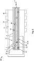
- Fig. 1 shows a cable 1 according to the invention in a sectional view along a cable direction 2.
- the cable 1 extends along the cable direction 2 and has at least one cable core 4, which is encased at least partially by an insulation 6.
- an electrical conductor 8 which is schematically depicted in Fig. 1 , the cable core 4 is exposed in a contact zone 10.
- the contact zone 10 is filled so that a surface 12 of the contact zone 10 is arranged substantially flush with the surface 14 of the cable 1, in particular the insulation 6.
- the surface 12 of the contact zone 10 can be pushed against the electrical conductor 8 without great difficulty and without deforming the cable core 4. It is consequently possible, at the contact zone 10, to keep the distance between the contact zone 10 and the electrical conductor 8 small and to connect the cable 1 to the electrical conductor 8 preferably by means of laser welding methods.
- an electrically conductive contact material 16 can be applied galvanically onto the cable core 4, so that not only a mechanical connection between the cable 1 and the electrical conductor 8, but also an electrically conductive connection, is produced in the contact zone 10.
- the electrically conductive contact material 16 can be applied preferably galvanically, for example by means of a reverse pulse plating. It is particularly advantageous if the cable core 4 is formed from substantially the same contact material 16, so that no electrical multiphase system arises between a filling 18 of the contact zone 10 and the cable core 4. "Substantially” here means that the cable core 4 and the electrically conductive contact material 16 possess the same main component, and thus the cable core 4 for example can be formed from a copper alloy and the electrically conductive contact material 16 can be a different copper alloy.
- the contact zone 10 which is filled substantially flush with the surface 14, the contact zone can be held down without great difficulty, for example for laser welding. As a result, it is possible to keep a width 20 of the contact zone 10 small compared to a contact zone at which the cable 1 is connected to the electrical conductor 8 by means of laser welding. In the case of the known ultrasound welding, the cable core 4 is pushed against the electrical conductor 8 with a sonotrode, and therefore the width of the contact zone 10 must be sufficiently large to allow the sonotrode to be placed on the cable core.
- the contact zone 10 can for example have a width 20 of a maximum of approximately 0.8 mm.
- the cable 1 is a flat cable 22, in which several cable cores 4 are arranged parallel alongside one another on a level plane (see Fig. 2 ).
- the flat cable 22 is preferably a flexible flat cable (FFC), in which the cable cores 4 are configured as metal strips 24 with a thickness 26 and a width 28.
- the flat cable 22 can extend over the electrical conductor 8 and each cable core 4 can be connected to the electrical conductor 8.
- each cable core 4 is exposed at at least one dedicated contact zone 10.
- the contact zones 10 are arranged offset from one another in cable direction 2.
- the flat cable 22 can be connected to the electrical conductor 8, or also to different electrical conductors, at different positions along the cable direction 2.
- the contact zone 10 above and below the cable core 4 is filled perpendicular to the cable direction 2, until its surface 12 is arranged substantially flush with the cable surface 14 on an underside 30 and an upper side 32 which is situated opposite the underside 30.
- the cable core 4 can thus be protectively encased by the filling 18.
- a force can be exerted on the cable 1 at the upper side 32, in order to hold the contact zone 10 down during the joining process, without additionally stressing or deforming the cable core 4. Since a deformation of the cable core 4 is avoided, the thickness 26 of the cable core 4 can be minimised to approximately 0.075 mm.
- a cable core 4 with such a thickness 26 could tear in the event of a deformation, for example, as a result of pressing down with a sonotrode.
- the cable 1 can thus be arranged at a contact zone below an electrical conductor 8, or above.
- Figure 2 schematically depicts a cable connection 34 according to the invention in a plan view.
- the cable 1 is a flexible flat cable 22 which is laid onto the electrical conductor 8 and which extends over this in the cable direction 2.
- the electrical conductor 8 is, for example, a cell connector 36 which connects together individual battery cells 38 which are arranged in rows.
- each cable core 4 has at least two contact zones 10 spaced apart from one another in the cable direction.
- the cable core 4 can be connected to the electrical conductor 8 in one contact zone 10 and to a further conductor, for example a circuit board 40, in the other contact zone 10.
- the cable cores 4 which lie alongside one another are preferably supplied with contact zones 10 which are offset from one another, so that in each case a cable core 4, at the height of a battery cell 38, can be connected to the electrical conductor 8.
- the contact zones 10 are arranged offset from one another in cable direction 2 for connection to the circuit board 40. As a result, it is possible to prevent unintentional bridging between the cable cores 4 when soldering or welding.
- the contact zones 10 can be configured such that they are suitable to receive a solder ball (not shown).
- the circuit board 40 can be supplied with solder balls which can be placed onto the contact zone 10 in order to produce a simple and efficient solder connection between the circuit board 40 and the contact zone 10.
- a width 20 of the contact zone 10 can be greater than the width of the solder ball.
- the filling 18 is stable and does not become deformed through the pressing-on of the solder ball.
- the contact zone 10 preferably has a round cross-section 44.
- the filled contact zone 10 thus substantially describes a cylinder 46.
- a central axis of the cable core 4 can be arranged substantially perpendicular to the cylinder axis and can intersect it.
- the width 20 of the contact zone 10 can be greater than the width 28 of the cable core 4.
- the cable core 4 can be protectively surrounded by the filling 18 in the contact zone 10.
- the width 20 of the contact zone 10 can also be smaller than the width 28 of the cable core 4.
- the contact zone 10 is further minimised, which makes it possible to further miniaturise the cable 1 and the cable connection 34.
- the space required to hold down the cable 1 can be significantly reduced.
- the contact zone 10 can be pushed against the electrical conductor 8 and can be connected to the electrical conductor 8 preferably by means of laser welding. As a result, a significantly smaller welding point is obtained compared to ultrasound welding, in which case a sonotrode has to be placed onto the welding point.
Landscapes
- Engineering & Computer Science (AREA)
- Manufacturing & Machinery (AREA)
- Connections Effected By Soldering, Adhesion, Or Permanent Deformation (AREA)
- Multi-Conductor Connections (AREA)
- Chemical & Material Sciences (AREA)
- Chemical Kinetics & Catalysis (AREA)
- Electrochemistry (AREA)
- General Chemical & Material Sciences (AREA)
Abstract
Description
- The invention relates to a cable with at least one electrically conductive cable core and one insulation that at least partially encases the at least one cable core, wherein the cable has at least one contact zone for contacting an electrical conductor and wherein the at least one cable core is exposed in the at least one contact zone. Furthermore, the invention relates to a method of manufacturing such a cable and to a cable connection between the cable and an electrical conductor.
- Such cables are connected, in particular through ultrasound welding, to cell connectors of battery cells in a motor vehicle, for example, for the purpose of measuring difference in potential. In the case of ultrasound welding, a sonotrode is placed onto the contact zone. By introducing high-frequency mechanical vibrations, the sonotrode is caused to produce resonation which can be transferred to the contact zone. By virtue of the high frequency and the pressure, friction gives rise to an atomic connection between the contact zone and the electrical conductor. For this purpose, a minimum size of contact zone is required, so that the sonotrode can be placed on. Miniaturisation of the cable is thus prevented by the size of the contact zone.
- Consequently, the object of the invention is to create a cable or a cable connection with as small a contact zone as possible. Moreover, the object of the invention is to provide a method of producing such a cable.
- The object is achieved according to the invention for the above-mentioned cable in that the contact zone is filled such that a surface of the contact zone is arranged substantially flush with a cable surface.
- Furthermore, the object is achieved through a cable connection according to the invention, in that the cable according to the invention and an electrical conductor are connected to one another at the contact zone by a laser welding connection.
- According to the invention, the cable is manufactured by filling the contact zone until a surface of the contact zone is arranged substantially flush with a cable surface.
- By virtue of the solution according to the invention, it is possible to hold the cable down on the contact zone without great effort. Therefore, the contact zone can be pushed against the electrical conductor and be connected to the electrical conductor, in particular by laser welding.
- Therefore, it is no longer necessary to dimension the contact zone such that a sonotrode can be placed on. Due to the contact zone miniaturisation which is achieved as a result, the size of the cable can be reduced further. A further advantage through the filling of the contact zone until the surface of the contact zone is arranged substantially flush with the cable surface is that the cable core no longer has to be deformed, in particular no longer has to be pushed against the electrical conductor in order to contact the electrical conductor. As a result, the cable core can be prevented from tearing during connection and it is also possible to use cable cores which are relatively less thick.
- Hereafter, further developments are cited which can be combined with one another independently of one another as desired and which are each advantageous viewed independently.
- Therefore, according to a first advantageous configuration, for example, an electrically conducting contact material can be applied in the contact zone. Thus, not only a mechanical connection, but also an electrically conducting connection, can be produced between the electrical conductor and the cable.
- The at least one cable core can preferably likewise be formed from the electrically conducting contact material. As a result, a homogeneous electrical system is created and contact corrosion between the contact material which fills the contact zone, and the cable core is avoided. Furthermore, this can lead to a simple cable connection design.
- According to a further advantageous configuration, the at least one contact zone can be galvanically coated until the surface of the at least one contact zone is arranged substantially flush with the cable surface. The contact zone can be galvanically coppered, for example, in particular by means of reverse pulse plating or by means of via plating. As a result, the contact zone can be filled simply and precisely.
- In order to keep the size of the at least one contact zone to a minimum, according to a further advantageous configuration, the at least one contact zone can have a width of a maximum of approximately 0.8 mm. As a result, the user acquires greater freedom in designing the cable connection, since with such a small contact zone a greater degree of tolerance is obtained in the positioning thereof relative to the electrical conductor.
- According to a further advantageous configuration, the cable can have at least two cable cores arranged alongside one another, and in particular electrically insulated from one another, wherein each cable core can be exposed in at least one contact zone. Preferably, the contact zones at which the adjacent cable cores are exposed are spaced apart and/or separated from one another. As a result, several connections can be manufactured between the cable and the electrical conductor. For example, an electrical conductor can be contacted at various points by different cable cores or it is also possible for several electrical conductors to be contacted by the cable, with one cable core respectively being connected to one electrical conductor.
- In particular, the contact zones of the at least two cable cores can be arranged offset from one another. The contact zones of the at least two cable cores can preferably be arranged offset from one another in a cable direction, along which the at least two cable cores extend. Soldering bridges can thus be avoided, in particular during soldering. If the contact zones are arranged offset from one another, the cable cores situated alongside one another can be brought closer to one another, without running the risk of unintentional bridge connection arising between the cable cores. Therefore, through offset contact zones, the dimensions of the cable, in particular its width, can be reduced.
- In a particularly advantageous configuration, each cable core is exposed at at least two contact zones. There are thus at least two attachment possibilities for each cable core. The at least two contact zones are preferably spaced apart from one another in the cable direction. For example, the cable core can thus be connected to an electrical conductor, such as a cell connector of a battery module, at the first contact zone and to a circuit board at the second contact zone.
- The cable can preferably be configured as a flat cable, in particular as a flexible flat cable, in which several cable cores are arranged parallel to one another on a level plane. Each cable core can be connected to a separate electrical conductor, or to the electrical conductor at points which are spaced apart from one another in the cable direction. Thus, for example, at least one cable core can be provided for each battery cell in a battery module which is constructed from several battery cells which are arranged in rows and connected by means of a cell connector. The flat cable can furthermore be soldered onto a circuit board, as a result of which, for example, the potential difference between the individual battery cells can be simply measured. The contact zone can be reduced in size as a result of the contact zone which is filled substantially flush with the cable surface in accordance with the invention. As a result, the flat cable can be equipped with a larger number of cable cores, for example, as a result of which the number of battery cells contacted by the flat cable increases, without increasing the width of the flat cable compared to conventional flat cables. The width of a cable core can thus be smaller than approximately 1 mm.
- According to a further advantageous configuration, the at least one contact zone can be filled up on both sides substantially flush with the cable surface. The contact zone can therefore be filled up particularly above and below the cable core. The cable core is thus strengthened at the contact zone and the cable can be pushed against the electrical conductor from above without any problems. As a result, the cable core can have a comparatively smaller thickness, for example 0.075 mm, as the cable core does not have to be deformed for connection to the electrical conductor and is fixed in its position and protected by the contact zone which is filled up on both sides. Furthermore, the cable core and/or the flat cable can have a uniform thickness over the cable direction, as a result of which it is possible to guarantee safety from twisting, in particular when rolling up the cable core and/or the flat cable.
- The at least one contact zone can preferably be circular, in particular in a cross-section along the cable direction. The filled-up contact zone thus substantially describes a cylinder. In particular, a central axis can be arranged substantially perpendicular to the cylinder axis and intersect it. As a result, it can be guaranteed that the cable core is exposed symmetrically in the contact zone and a uniform connection to the electrical conductor can be produced.
- At least one contact zone can be supplied with a solder ball and/or a solder ball can be placed onto at least one contact zone. This can simplify the soldering of the cable onto a circuit board, for example. Alternatively, the cable can be connected to the contact zone by means of a laser-welded connection to the circuit board.
- The contact zone can be galvanically filled, for example by way of electroplating. As a result, a precise and cost-efficient filling of the contact zone is possible. The contact zone can preferably be filled up by means of reverse pulse plating or via plating.
- The cable connection can have at least one further electrical conductor, for example a circuit board which is connected to the cable at at least one contact zone. In this case, the circuit board can be soldered onto the contact zone or can have a welded connection through laser welding, for example.
- The cable can extend along the cable direction over the electrical conductor and can be connected to the electrical conductor at contact zones which are offset from one another along the cable direction. As a result, it is possible to prevent the contact zones of the cable cores from being arranged in a straight line perpendicular to the cable direction, and to prevent unintentional bridging from occurring during connection.
- Hereinafter, the invention is described in greater detail by way of example using exemplary embodiments with reference to the attached figures. In the figures, elements which correspond to one another in design and/or function are provided with the same reference symbols.
- The combination of features shown and described with the individual exemplary embodiments serves solely the purposes of explanation. In accordance with the statements above, it is possible to dispense with a feature from an exemplary embodiment if this technical effect is of no importance in a particular application. Conversely, according to the above statements a further feature can be added in an exemplary embodiment if this technical feature is meant to be advantageous or necessary to a particular application.
- In the drawings:
-
Fig. 1 shows a schematic sectional view of a cable according to the invention; and -
Fig. 2 shows a schematic plan view of a cable connection according to the invention. -
Fig. 1 shows acable 1 according to the invention in a sectional view along acable direction 2. - The
cable 1 extends along thecable direction 2 and has at least onecable core 4, which is encased at least partially by aninsulation 6. In order to contact anelectrical conductor 8, which is schematically depicted inFig. 1 , thecable core 4 is exposed in acontact zone 10. - According to the invention, the
contact zone 10 is filled so that asurface 12 of thecontact zone 10 is arranged substantially flush with thesurface 14 of thecable 1, in particular theinsulation 6. As a result, thesurface 12 of thecontact zone 10 can be pushed against theelectrical conductor 8 without great difficulty and without deforming thecable core 4. It is consequently possible, at thecontact zone 10, to keep the distance between thecontact zone 10 and theelectrical conductor 8 small and to connect thecable 1 to theelectrical conductor 8 preferably by means of laser welding methods. - In the
contact zone 10, an electricallyconductive contact material 16 can be applied galvanically onto thecable core 4, so that not only a mechanical connection between thecable 1 and theelectrical conductor 8, but also an electrically conductive connection, is produced in thecontact zone 10. The electricallyconductive contact material 16 can be applied preferably galvanically, for example by means of a reverse pulse plating. It is particularly advantageous if thecable core 4 is formed from substantially thesame contact material 16, so that no electrical multiphase system arises between a filling 18 of thecontact zone 10 and thecable core 4. "Substantially" here means that thecable core 4 and the electricallyconductive contact material 16 possess the same main component, and thus thecable core 4 for example can be formed from a copper alloy and the electricallyconductive contact material 16 can be a different copper alloy. - By way of the
contact zone 10 which is filled substantially flush with thesurface 14, the contact zone can be held down without great difficulty, for example for laser welding. As a result, it is possible to keep awidth 20 of thecontact zone 10 small compared to a contact zone at which thecable 1 is connected to theelectrical conductor 8 by means of laser welding. In the case of the known ultrasound welding, thecable core 4 is pushed against theelectrical conductor 8 with a sonotrode, and therefore the width of thecontact zone 10 must be sufficiently large to allow the sonotrode to be placed on the cable core. Thecontact zone 10 can for example have awidth 20 of a maximum of approximately 0.8 mm. - According to a particularly advantageous configuration, the
cable 1 is aflat cable 22, in whichseveral cable cores 4 are arranged parallel alongside one another on a level plane (seeFig. 2 ). Theflat cable 22 is preferably a flexible flat cable (FFC), in which thecable cores 4 are configured as metal strips 24 with athickness 26 and awidth 28. Theflat cable 22 can extend over theelectrical conductor 8 and eachcable core 4 can be connected to theelectrical conductor 8. For this purpose, eachcable core 4 is exposed at at least onededicated contact zone 10. In this case, it is particularly advantageous if thecontact zones 10 are arranged offset from one another incable direction 2. As a result of this, theflat cable 22 can be connected to theelectrical conductor 8, or also to different electrical conductors, at different positions along thecable direction 2. - As can be seen in
Fig. 1 , it is particularly advantageous if thecontact zone 10 above and below thecable core 4 is filled perpendicular to thecable direction 2, until itssurface 12 is arranged substantially flush with thecable surface 14 on anunderside 30 and anupper side 32 which is situated opposite theunderside 30. Thecable core 4 can thus be protectively encased by the filling 18. A force can be exerted on thecable 1 at theupper side 32, in order to hold thecontact zone 10 down during the joining process, without additionally stressing or deforming thecable core 4. Since a deformation of thecable core 4 is avoided, thethickness 26 of thecable core 4 can be minimised to approximately 0.075 mm. Acable core 4 with such athickness 26 could tear in the event of a deformation, for example, as a result of pressing down with a sonotrode. - By way of the
contact zone 10 which is filled on both sides substantially flush with thecable surface 14, the user is given greater freedom when designing his cable connection. Thecable 1 can thus be arranged at a contact zone below anelectrical conductor 8, or above. -
Figure 2 schematically depicts acable connection 34 according to the invention in a plan view. - The
cable 1 is a flexibleflat cable 22 which is laid onto theelectrical conductor 8 and which extends over this in thecable direction 2. Theelectrical conductor 8 is, for example, acell connector 36 which connects togetherindividual battery cells 38 which are arranged in rows. - In this advantageous configuration, each
cable core 4 has at least twocontact zones 10 spaced apart from one another in the cable direction. Thecable core 4 can be connected to theelectrical conductor 8 in onecontact zone 10 and to a further conductor, for example acircuit board 40, in theother contact zone 10. Thecable cores 4 which lie alongside one another are preferably supplied withcontact zones 10 which are offset from one another, so that in each case acable core 4, at the height of abattery cell 38, can be connected to theelectrical conductor 8. - In this case, it has proven to be particularly advantageous if the
contact zones 10 are arranged offset from one another incable direction 2 for connection to thecircuit board 40. As a result, it is possible to prevent unintentional bridging between thecable cores 4 when soldering or welding. - The
contact zones 10 can be configured such that they are suitable to receive a solder ball (not shown). For example, thecircuit board 40 can be supplied with solder balls which can be placed onto thecontact zone 10 in order to produce a simple and efficient solder connection between thecircuit board 40 and thecontact zone 10. For this purpose, awidth 20 of thecontact zone 10 can be greater than the width of the solder ball. Furthermore, it is advantageous if the filling 18 is stable and does not become deformed through the pressing-on of the solder ball. - In a plan view, the
contact zone 10 preferably has around cross-section 44. The filledcontact zone 10 thus substantially describes acylinder 46. In particular, a central axis of thecable core 4 can be arranged substantially perpendicular to the cylinder axis and can intersect it. As a result, it can be guaranteed that thecable core 4 is exposed symmetrically in thecontact zone 10 and a uniform connection to theelectrical conductor 8 can be produced. Thewidth 20 of thecontact zone 10, as is depicted inFig. 2 , can be greater than thewidth 28 of thecable core 4. As a result of this, thecable core 4 can be protectively surrounded by the filling 18 in thecontact zone 10. Alternatively, thewidth 20 of thecontact zone 10 can also be smaller than thewidth 28 of thecable core 4. As a result, thecontact zone 10 is further minimised, which makes it possible to further miniaturise thecable 1 and thecable connection 34. - By virtue of the
cable 1 according to the invention, with at least onecontact zone 10 filled up to thecable surface 14, the space required to hold down thecable 1 can be significantly reduced. Thecontact zone 10 can be pushed against theelectrical conductor 8 and can be connected to theelectrical conductor 8 preferably by means of laser welding. As a result, a significantly smaller welding point is obtained compared to ultrasound welding, in which case a sonotrode has to be placed onto the welding point. -
- 1
- cable
- 2
- cable direction
- 4
- cable core
- 6
- insulation
- 8
- electrical conductor
- 10
- contact zone
- 12
- surface of the contact zone
- 14
- surface of the cable
- 16
- contact material
- 18
- filling
- 20
- width of the contact zone
- 22
- flat cable
- 24
- metal strips
- 26
- thickness
- 28
- width of the cable core
- 30
- underside
- 32
- upper side
- 34
- cable connection
- 36
- cell connector
- 38
- battery cells
- 40
- circuit board
- 44
- cross-section
- 46
- cylinder
Claims (15)
- A cable (1) with at least one electrically conductive cable core (4) and one insulation (6) that at least partially encases the at least one cable core (4), wherein the cable (1) has at least one contact zone (10) for contacting an electrical conductor (8) and wherein the at least one cable core (4) is exposed in the at least one contact zone (10), characterised in that a surface (12) of the contact zone (10) is filled up substantially flush with a cable surface (14).
- The cable (1) according to Claim 1, characterised in that an electrically conducting contact material (16) is applied onto the cable core (4) in the contact zone (10).
- The cable (1) according to Claim 2, characterised in that the at least one cable core (4) is formed from the electrically conducting contact material (16).
- The cable (1) according to any one of Claims 1 to 3, characterised in that the at least one contact zone (10) is galvanically filled up to the surface (12) of the contact zone (10) substantially flush with the cable surface (14).
- The cable (1) according to any one of Claims 1 to 4, characterised in that the contact zone (10) has a width (20) of a maximum of 0.8 mm.
- The cable (1) according to any one of Claims 1 to 5, characterised in that the cable (1) has at least two cable cores (4) arranged alongside one another and in that each cable core (4) is supplied with at least one contact zone (10).
- The cable (1) according to Claim 6, characterised in that the contact zones (10) of the at least two cable cores (4) are separated from one another.
- The cable (1) according to Claim 6 or 7, characterised in that the contact zones (10) of the at least two cable cores (4) are arranged offset from one another.
- The cable (1) according to any one of Claims 1 to 8, characterised in that the at least one cable core (4) is exposed in at least two contact zones (10).
- The cable (1) according to any one of Claims 1 to 9, characterised in that the cable (1) is a flat cable (22).
- The cable (1) according to Claim 10, characterised in that the surface (12) of the at least one contact zone (10) is filled up on both sides substantially flush with the cable surface (14).
- The cable (1) according to any one of Claims 9 to 11, characterised in that the at least one contact zone (10) has a substantially circular cross section (44).
- A method for manufacturing a cable (1) with at least one electrically conductive cable core (1) and one insulation (6) that at least partially encases the at least one cable core (4), wherein the cable (1) has at least one contact zone (10) for contacting an electrical conductor (8) and wherein the at least one cable core (4) is exposed in the at least one contact zone (10), characterised in that the at least one contact zone (10) is filled up to a surface (12) of the contact zone (10) substantially flush with the cable surface (14).
- The method according to Claim 13, characterised in that the at least one contact zone (10) is filled galvanically.
- A cable connection (34) comprising an electrical conductor (8) and a cable (1) according to any one of Claims 1 to 12, characterised in that the cable (1) has a laser weld connection at at least one contact zone (10) with the electrical conductor (8).
Applications Claiming Priority (1)
| Application Number | Priority Date | Filing Date | Title |
|---|---|---|---|
| DE102019202061.5A DE102019202061A1 (en) | 2019-02-15 | 2019-02-15 | Cable and method of making the cable |
Publications (1)
| Publication Number | Publication Date |
|---|---|
| EP3696919A1 true EP3696919A1 (en) | 2020-08-19 |
Family
ID=69630148
Family Applications (1)
| Application Number | Title | Priority Date | Filing Date |
|---|---|---|---|
| EP20157411.8A Pending EP3696919A1 (en) | 2019-02-15 | 2020-02-14 | Cable and method for manufacturing the cable |
Country Status (4)
| Country | Link |
|---|---|
| US (1) | US11127511B2 (en) |
| EP (1) | EP3696919A1 (en) |
| CN (1) | CN111585138B (en) |
| DE (1) | DE102019202061A1 (en) |
Citations (5)
| Publication number | Priority date | Publication date | Assignee | Title |
|---|---|---|---|---|
| US6020559A (en) * | 1996-12-02 | 2000-02-01 | Funai Electric Co., Ltd. | Flat flexible cable |
| EP1256408A1 (en) * | 2001-03-28 | 2002-11-13 | Visteon Global Technologies, Inc. | Soldering method for joining flex circuits by diode laser |
| US20040055784A1 (en) * | 2002-02-20 | 2004-03-25 | Joshi Prashant P. | Solder interconnections for flat circuits |
| US20050057262A1 (en) * | 2003-09-12 | 2005-03-17 | International Business Machines | Method for testing integrity of electrical connection of a flat cable multiple connector assembly |
| US20140246068A1 (en) * | 2013-03-04 | 2014-09-04 | Robert Bosch Gmbh | Metal connector profile, solar module and method for its manufacture |
Family Cites Families (18)
| Publication number | Priority date | Publication date | Assignee | Title |
|---|---|---|---|---|
| US3070650A (en) * | 1960-09-23 | 1962-12-25 | Sanders Associates Inc | Solder connection for electrical circuits |
| US3680209A (en) * | 1969-05-07 | 1972-08-01 | Siemens Ag | Method of forming stacked circuit boards |
| US4407065A (en) * | 1980-01-17 | 1983-10-04 | Gray Stanley J | Multiple sheath cable and method of manufacture |
| US5900587A (en) * | 1994-12-02 | 1999-05-04 | Piper; Douglas E. | Daisy chain cable assembly and method for manufacture |
| JP2000252598A (en) * | 1999-03-02 | 2000-09-14 | Fuji Photo Film Co Ltd | Flexible printed-wiring board |
| DE10224713A1 (en) * | 2002-06-04 | 2003-12-18 | Daimler Chrysler Ag | Repair system for flexible flat electrical cable has additional stretch of flat cable laid over gap after damaged section has been cut out with individual wire ends connected together by solder paste |
| JP4013691B2 (en) * | 2002-07-31 | 2007-11-28 | 住友電装株式会社 | Flexible flat cable connection method and ultrasonic welding machine |
| DE10307846A1 (en) | 2003-02-25 | 2004-09-02 | Daimlerchrysler Ag | Method for electrically contacting a component with a flat cable |
| US7223919B2 (en) * | 2004-05-11 | 2007-05-29 | Gagne Norman P | Flat flexible cable with integrated stiffener |
| US7622677B2 (en) * | 2006-09-26 | 2009-11-24 | Accutru International Corporation | Mineral insulated metal sheathed cable connector and method of forming the connector |
| KR20100110937A (en) | 2009-04-06 | 2010-10-14 | 아주대학교산학협력단 | Plating method for flexible flat cable by the conductive paste |
| CN201525897U (en) | 2009-08-19 | 2010-07-14 | 许煜炜 | FFC galvanizing device |
| TW201124007A (en) * | 2009-12-30 | 2011-07-01 | Au Optronics Corp | Substrate and substrate bonding device using the same |
| JP5654088B1 (en) | 2013-07-08 | 2015-01-14 | 日本発條株式会社 | Conductive member and method of manufacturing conductive member |
| JP6244147B2 (en) | 2013-09-18 | 2017-12-06 | エスアイアイ・セミコンダクタ株式会社 | Manufacturing method of semiconductor device |
| US9877391B2 (en) * | 2015-10-05 | 2018-01-23 | Kabushiki Kaisha Toshiba | Electronic module comprising flexible conducting member connected thereto and method of connecting flexible conducting member to electronic module |
| DE102016102948A1 (en) * | 2016-02-19 | 2017-08-24 | PKC SEGU Systemelektrik GmbH | Method and device for sealing contact points on electrical line connections |
| CN108109954B (en) | 2016-11-25 | 2021-04-23 | 中芯国际集成电路制造(上海)有限公司 | Manufacturing method of interconnect structure |
-
2019
- 2019-02-15 DE DE102019202061.5A patent/DE102019202061A1/en active Pending
-
2020
- 2020-02-13 US US16/790,054 patent/US11127511B2/en active Active
- 2020-02-14 EP EP20157411.8A patent/EP3696919A1/en active Pending
- 2020-02-17 CN CN202010095901.9A patent/CN111585138B/en active Active
Patent Citations (6)
| Publication number | Priority date | Publication date | Assignee | Title |
|---|---|---|---|---|
| US6020559A (en) * | 1996-12-02 | 2000-02-01 | Funai Electric Co., Ltd. | Flat flexible cable |
| EP1256408A1 (en) * | 2001-03-28 | 2002-11-13 | Visteon Global Technologies, Inc. | Soldering method for joining flex circuits by diode laser |
| EP1256408B1 (en) * | 2001-03-28 | 2005-07-27 | Visteon Global Technologies, Inc. | Method of soldering plastic flex circuits boards by diode laser |
| US20040055784A1 (en) * | 2002-02-20 | 2004-03-25 | Joshi Prashant P. | Solder interconnections for flat circuits |
| US20050057262A1 (en) * | 2003-09-12 | 2005-03-17 | International Business Machines | Method for testing integrity of electrical connection of a flat cable multiple connector assembly |
| US20140246068A1 (en) * | 2013-03-04 | 2014-09-04 | Robert Bosch Gmbh | Metal connector profile, solar module and method for its manufacture |
Also Published As
| Publication number | Publication date |
|---|---|
| DE102019202061A1 (en) | 2020-08-20 |
| US11127511B2 (en) | 2021-09-21 |
| US20200265970A1 (en) | 2020-08-20 |
| CN111585138A (en) | 2020-08-25 |
| CN111585138B (en) | 2024-08-30 |
Similar Documents
| Publication | Publication Date | Title |
|---|---|---|
| JP6572304B2 (en) | Battery wiring module and power supply device including the battery wiring module | |
| JP7124968B2 (en) | Connection structure between flexible substrate and bus bar, wiring module, and power storage module | |
| US4662702A (en) | Electric contacts and electric connectors | |
| EP2913897B1 (en) | Connector structure, female connector and male connector | |
| CN102185188B (en) | Method for producing connector | |
| JP7248116B2 (en) | Wiring module and storage module | |
| KR102344935B1 (en) | Battery sensing module | |
| US10784642B2 (en) | Flexible printed wiring board, electronic device having flexible printed wiring board, and method for manufacturing electronic device having flexible printed wiring board | |
| EP2963739A1 (en) | Dual thickness double-ended male blade terminal | |
| CN118921842B (en) | Circuit board assembly for battery device | |
| US11127511B2 (en) | Cable and method for manufacturing the cable | |
| JP2014096260A (en) | Flat wiring material and mounting body using it | |
| JP5622051B2 (en) | Board terminal and board connector using the same | |
| CN102379165A (en) | Conductor grid for an electronic housing and method for producing the same | |
| JP5330924B2 (en) | Connection structure and connection method between flat substrate and connection terminal | |
| JPH115182A (en) | Laser welding material and laser welding structure | |
| US20220272839A1 (en) | Flexible printed wiring board, battery wiring module, and method of manufacturing flexible printed wiring board | |
| JP7001561B2 (en) | Flat wire connection structure | |
| US12279367B2 (en) | Wiring circuit board and producing method thereof | |
| US7384270B2 (en) | Electrical connector | |
| CN121312011A (en) | Wiring module | |
| WO2024062562A1 (en) | Cantilever-type probe for probe card, and probe card | |
| JP4100998B2 (en) | Connection part and connection method between printed circuit board and flat cable | |
| JP2008084806A (en) | Conductive connection member | |
| JP2020161469A (en) | Electronic devices and pressure welding terminals |
Legal Events
| Date | Code | Title | Description |
|---|---|---|---|
| PUAI | Public reference made under article 153(3) epc to a published international application that has entered the european phase |
Free format text: ORIGINAL CODE: 0009012 |
|
| STAA | Information on the status of an ep patent application or granted ep patent |
Free format text: STATUS: THE APPLICATION HAS BEEN PUBLISHED |
|
| AK | Designated contracting states |
Kind code of ref document: A1 Designated state(s): AL AT BE BG CH CY CZ DE DK EE ES FI FR GB GR HR HU IE IS IT LI LT LU LV MC MK MT NL NO PL PT RO RS SE SI SK SM TR |
|
| AX | Request for extension of the european patent |
Extension state: BA ME |
|
| STAA | Information on the status of an ep patent application or granted ep patent |
Free format text: STATUS: REQUEST FOR EXAMINATION WAS MADE |
|
| 17P | Request for examination filed |
Effective date: 20210212 |
|
| RBV | Designated contracting states (corrected) |
Designated state(s): AL AT BE BG CH CY CZ DE DK EE ES FI FR GB GR HR HU IE IS IT LI LT LU LV MC MK MT NL NO PL PT RO RS SE SI SK SM TR |
|
| STAA | Information on the status of an ep patent application or granted ep patent |
Free format text: STATUS: EXAMINATION IS IN PROGRESS |
|
| 17Q | First examination report despatched |
Effective date: 20220207 |