EP3696859A1 - Organic light emitting display device - Google Patents
Organic light emitting display device Download PDFInfo
- Publication number
- EP3696859A1 EP3696859A1 EP20156245.1A EP20156245A EP3696859A1 EP 3696859 A1 EP3696859 A1 EP 3696859A1 EP 20156245 A EP20156245 A EP 20156245A EP 3696859 A1 EP3696859 A1 EP 3696859A1
- Authority
- EP
- European Patent Office
- Prior art keywords
- layer
- light emitting
- pattern
- insulating layer
- opening
- Prior art date
- Legal status (The legal status is an assumption and is not a legal conclusion. Google has not performed a legal analysis and makes no representation as to the accuracy of the status listed.)
- Pending
Links
Images










Classifications
-
- H—ELECTRICITY
- H10—SEMICONDUCTOR DEVICES; ELECTRIC SOLID-STATE DEVICES NOT OTHERWISE PROVIDED FOR
- H10D—INORGANIC ELECTRIC SEMICONDUCTOR DEVICES
- H10D86/00—Integrated devices formed in or on insulating or conducting substrates, e.g. formed in silicon-on-insulator [SOI] substrates or on stainless steel or glass substrates
- H10D86/40—Integrated devices formed in or on insulating or conducting substrates, e.g. formed in silicon-on-insulator [SOI] substrates or on stainless steel or glass substrates characterised by multiple TFTs
- H10D86/411—Integrated devices formed in or on insulating or conducting substrates, e.g. formed in silicon-on-insulator [SOI] substrates or on stainless steel or glass substrates characterised by multiple TFTs characterised by materials, geometry or structure of the substrates
-
- H—ELECTRICITY
- H10—SEMICONDUCTOR DEVICES; ELECTRIC SOLID-STATE DEVICES NOT OTHERWISE PROVIDED FOR
- H10K—ORGANIC ELECTRIC SOLID-STATE DEVICES
- H10K59/00—Integrated devices, or assemblies of multiple devices, comprising at least one organic light-emitting element covered by group H10K50/00
- H10K59/10—OLED displays
- H10K59/12—Active-matrix OLED [AMOLED] displays
- H10K59/124—Insulating layers formed between TFT elements and OLED elements
-
- H—ELECTRICITY
- H10—SEMICONDUCTOR DEVICES; ELECTRIC SOLID-STATE DEVICES NOT OTHERWISE PROVIDED FOR
- H10K—ORGANIC ELECTRIC SOLID-STATE DEVICES
- H10K59/00—Integrated devices, or assemblies of multiple devices, comprising at least one organic light-emitting element covered by group H10K50/00
- H10K59/80—Constructional details
- H10K59/87—Passivation; Containers; Encapsulations
-
- H—ELECTRICITY
- H10—SEMICONDUCTOR DEVICES; ELECTRIC SOLID-STATE DEVICES NOT OTHERWISE PROVIDED FOR
- H10D—INORGANIC ELECTRIC SEMICONDUCTOR DEVICES
- H10D86/00—Integrated devices formed in or on insulating or conducting substrates, e.g. formed in silicon-on-insulator [SOI] substrates or on stainless steel or glass substrates
- H10D86/40—Integrated devices formed in or on insulating or conducting substrates, e.g. formed in silicon-on-insulator [SOI] substrates or on stainless steel or glass substrates characterised by multiple TFTs
- H10D86/60—Integrated devices formed in or on insulating or conducting substrates, e.g. formed in silicon-on-insulator [SOI] substrates or on stainless steel or glass substrates characterised by multiple TFTs wherein the TFTs are in active matrices
-
- H—ELECTRICITY
- H10—SEMICONDUCTOR DEVICES; ELECTRIC SOLID-STATE DEVICES NOT OTHERWISE PROVIDED FOR
- H10K—ORGANIC ELECTRIC SOLID-STATE DEVICES
- H10K50/00—Organic light-emitting devices
- H10K50/80—Constructional details
- H10K50/84—Passivation; Containers; Encapsulations
- H10K50/844—Encapsulations
- H10K50/8445—Encapsulations multilayered coatings having a repetitive structure, e.g. having multiple organic-inorganic bilayers
-
- H—ELECTRICITY
- H10—SEMICONDUCTOR DEVICES; ELECTRIC SOLID-STATE DEVICES NOT OTHERWISE PROVIDED FOR
- H10K—ORGANIC ELECTRIC SOLID-STATE DEVICES
- H10K59/00—Integrated devices, or assemblies of multiple devices, comprising at least one organic light-emitting element covered by group H10K50/00
- H10K59/10—OLED displays
- H10K59/12—Active-matrix OLED [AMOLED] displays
- H10K59/121—Active-matrix OLED [AMOLED] displays characterised by the geometry or disposition of pixel elements
-
- H—ELECTRICITY
- H10—SEMICONDUCTOR DEVICES; ELECTRIC SOLID-STATE DEVICES NOT OTHERWISE PROVIDED FOR
- H10K—ORGANIC ELECTRIC SOLID-STATE DEVICES
- H10K59/00—Integrated devices, or assemblies of multiple devices, comprising at least one organic light-emitting element covered by group H10K50/00
- H10K59/10—OLED displays
- H10K59/12—Active-matrix OLED [AMOLED] displays
- H10K59/122—Pixel-defining structures or layers, e.g. banks
-
- H—ELECTRICITY
- H10—SEMICONDUCTOR DEVICES; ELECTRIC SOLID-STATE DEVICES NOT OTHERWISE PROVIDED FOR
- H10K—ORGANIC ELECTRIC SOLID-STATE DEVICES
- H10K59/00—Integrated devices, or assemblies of multiple devices, comprising at least one organic light-emitting element covered by group H10K50/00
- H10K59/80—Constructional details
- H10K59/87—Passivation; Containers; Encapsulations
- H10K59/873—Encapsulations
- H10K59/8731—Encapsulations multilayered coatings having a repetitive structure, e.g. having multiple organic-inorganic bilayers
-
- H—ELECTRICITY
- H10—SEMICONDUCTOR DEVICES; ELECTRIC SOLID-STATE DEVICES NOT OTHERWISE PROVIDED FOR
- H10K—ORGANIC ELECTRIC SOLID-STATE DEVICES
- H10K59/00—Integrated devices, or assemblies of multiple devices, comprising at least one organic light-emitting element covered by group H10K50/00
- H10K59/80—Constructional details
- H10K59/8791—Arrangements for improving contrast, e.g. preventing reflection of ambient light
- H10K59/8792—Arrangements for improving contrast, e.g. preventing reflection of ambient light comprising light absorbing layers, e.g. black layers
-
- H—ELECTRICITY
- H10—SEMICONDUCTOR DEVICES; ELECTRIC SOLID-STATE DEVICES NOT OTHERWISE PROVIDED FOR
- H10K—ORGANIC ELECTRIC SOLID-STATE DEVICES
- H10K71/00—Manufacture or treatment specially adapted for the organic devices covered by this subclass
Definitions
- Example embodiments relate generally to an organic light emitting display device and to an organic light emitting display device including functional modules that are in a part of a display region.
- a flat panel display device is used as a display device to replace a cathode ray tube display device because the flat panel display device is light weight and has thin features or the like.
- a liquid crystal display device and an organic light emitting display device are typical examples of the flat panel display device.
- the organic light emitting display device may include a display region configured to display an image and a non-display region surrounding the display region configured not to display the image.
- a plurality of light emitting structures may be disposed in the display region, and a gate driver, a data driver, a plurality of wires, a functional module (such as a camera module and a motion sensor) may be disposed in the non-display region.
- a functional module such as a camera module and a motion sensor
- an organic light emitting display device has been developed in which an opening is formed in a part of the display region and the functional module is disposed in the opening.
- moisture, humidity and the like can permeate through the opening into the light emitting structure, which is disposed in the display region adjacent to the functional module, and thus a defect may generate in the organic light emitting display device.
- OLED organic light emitting display
- an OLED device includes a substrate, a light emitting structure, an undercut structure, and a functional module.
- the substrate includes an opening region, a peripheral region surrounding the opening region, and a display region surrounding the peripheral region.
- the substrate has a groove in the peripheral region and an opening in the opening region.
- the light emitting structure is in the display region on the substrate.
- the undercut structure is inside the groove in the substrate, and includes a sacrificial metal pattern having a first width and at least one insulating layer pattern having a second width greater than the first width.
- the functional module is in the opening of the substrate.
- the undercut structure may be spaced apart from an inner wall of the groove.
- the groove may have a hollow circular shape surrounding the opening of the substrate in a plan view.
- the undercut structure may have a hollow circular shape surrounding the opening inside the groove in a plan view.
- the substrate may include a first organic film layer, a first barrier layer, a second organic film layer, and a second barrier layer.
- the first barrier layer may be on the first organic film layer.
- the second organic film layer may be on the first barrier layer, and may have a first opening in the peripheral region.
- the second barrier layer may be on the second organic film layer, and may have a second opening overlapping the first opening.
- the sacrificial metal pattern may be on the first barrier layer.
- the insulating layer pattern may include a first insulating layer pattern on the sacrificial metal pattern and a second insulating layer pattern on the first insulating layer pattern.
- the first insulating layer pattern may be located at a same layer as the second organic film layer, and the second insulating layer pattern may be located at a same layer as the second barrier layer.
- the first opening and the second opening may define the groove in the substrate.
- the OLED device may further include a semiconductor element between the substrate and the light emitting structure.
- the semiconductor element may include an active layer, a gate insulating layer, a gate electrode, an insulating interlayer, and source and drain electrodes.
- the active layer may be in the display region on the substrate.
- the gate insulating layer may cover the active layer in the display region on the substrate, and may have a third opening exposing the groove in the peripheral region.
- the gate electrode may be in the display region on the gate insulating layer.
- the insulating interlayer may cover the gate electrode in the display region on the gate insulating layer, and may have a fourth opening overlapping the third opening in the peripheral region.
- the source and drain electrodes may be in the display region on the insulating interlayer.
- the insulating layer pattern may include a third insulating layer pattern and a fourth insulating layer pattern.
- the third insulating layer pattern may be on the sacrificial metal pattern, and may be located inside the third opening.
- the fourth insulating layer pattern may be on the third insulating layer pattern, and may be located inside the fourth opening.
- the third insulating layer pattern may be located at a same layer as the gate insulating layer, and may be located at a same layer as the insulating interlayer.
- the light emitting structure may include a lower electrode, a light emitting layer on the lower electrode, and an upper electrode on the light emitting layer.
- the light emitting layer may extend in a direction from the display region to the peripheral region on the substrate, and may be short-circuited by the undercut structure at a portion where the groove is located.
- the upper electrode may extend in a direction from the display region to the peripheral region on the light emitting layer, and may be short-circuited by the undercut structure at a portion where the groove is located.
- the light emitting layer and the upper electrode may be at least partially inside of the groove.
- the light emitting layer and the upper electrode may be on at least a part of the undercut structure.
- the light emitting layer and the upper electrode might not be in direct contact with the sacrificial metal pattern.
- the OLED device may further include a thin film encapsulation structure disposed on the light emitting structure.
- the thin film encapsulation structure may include a first thin film encapsulation layer, a second thin film encapsulation layer, and a third thin film encapsulation layer.
- the first thin film encapsulation layer may be on the upper electrode, and may include a flexible inorganic material.
- the second thin film encapsulation layer may be on the first thin film encapsulation layer, and may include a flexible organic material.
- the third thin film encapsulation layer may be on the second thin film encapsulation layer, and may include the flexible inorganic material.
- each of the first and third thin film encapsulation layers may extend in a direction from the display region to the peripheral region on the upper electrode, and may be continuous at the portion where the groove is located.
- the functional module may be in contact with a side surface of the substrate, a side surface of the light emitting layer, a side surface of the upper electrode, a side surface of the first thin film encapsulation layer, and a side surface of the third thin encapsulation layer at a boundary between the peripheral region and the opening region.
- both side portions of the sacrificial metal pattern may be in direct contact with the first thin film encapsulation layer.
- the groove of the substrate may include a first groove located in the peripheral region and a second groove located between the first groove and the functional module.
- the first groove may surround the second groove.
- the undercut structure may include a first undercut structure inside the first groove and a second undercut structure inside the second groove.
- an organic light emitting display device as set out in claim 1. Additional features of this aspect are set out in claims 2 to 15.
- the OLED device includes the undercut structure inside the groove so that the OLED device can prevent or mitigate against moisture, humidity and the like from permeating or penetrating into the semiconductor element and the light emitting structure from the peripheral region to the display region.
- OLED organic light emitting display
- FIG. 1 is a perspective view showing an OLED device according to exemplary embodiments of the present invention.
- FIG. 2 is a plan view showing the OLED device of FIG. 1 .
- FIGS. 3 and 4 are perspective views depicting an opening formed in the OLED device of FIG. 1 .
- the OLED device 100 may include a functional module 700 or the like.
- the OLED device 100 may have a first surface S1 to display an image and a second surface S2 opposite to the first surface S1.
- the functional module 700 may be disposed on one side (e.g., the first surface S1) of the OLED device 100.
- the OLED device 100 may include a display region 10, an opening region 20, a peripheral region 30, and a pad region 40.
- the peripheral region 30 may substantially surround the opening region 20, and the display region 10 may substantially surround the peripheral region 30.
- the display region 10 might not completely surround the peripheral region 30.
- the OLED device 100 may include an opening 910 formed in the opening region 20.
- the pad region 40 may be located at one side or end of the display region 10.
- a plurality of pad electrodes may be disposed in the pad region 40, and the pad electrodes may be electrically connected to an external device.
- the OLED device 100 may further include a bending region located between the display region 10 and the pad region 40.
- the bending region may be bent about an axis with respect to a first direction D1 that is parallel to an upper surface of the OLED device 100, and the pad region 40 may be located on a bottom surface of the OLED device 100.
- the display region 10 may include a plurality of sub-pixel regions (not shown).
- the sub-pixel regions may be arrayed in the display region 10 to have a matrix form as a whole.
- a sub-pixel circuit (such as a semiconductor element 250 in FIG. 6 ) may be disposed in each of the sub-pixel regions of the display region 10, and an organic light emitting diode (such as a light emitting structure 200 in FIG. 6 ) may be disposed on the sub-pixel circuit.
- An image may be displayed on the display region 10 through the sub-pixel circuit and the organic light emitting diode.
- first, second, and third sub-pixel circuits may be disposed in the sub-pixel regions, and first, second, and third organic light emitting diodes may be disposed on the first to third sub-pixel circuits, respectively.
- the first sub-pixel circuit may be connected to the first organic light emitting diode capable of emitting red light
- the second sub-pixel circuit may be connected to the second organic light emitting diode capable of emitting green light
- the third sub-pixel circuit may be connected to the third organic light emitting diode capable of emitting blue light.
- the first organic light emitting diode may be disposed to overlap the first sub-pixel circuit
- the second organic light emitting diode may be disposed to overlap the second sub-pixel circuit
- the third organic light emitting diode may be disposed to overlap the third sub-pixel circuit.
- the first organic light emitting diode may be disposed to overlap a part of the first sub-pixel circuit and a part of a sub-pixel circuit different from the first sub-pixel circuit
- the second organic light emitting diode may be disposed to overlap a part of the second sub-pixel circuit and a part of a sub-pixel circuit different from the second sub-pixel circuit
- the third organic light emitting diode may be disposed to overlap a part of the third sub-pixel circuit and a part of a sub-pixel circuit different from the third sub-pixel circuit.
- the first to third organic light emitting diodes may be arrayed using a scheme such as an RGB stripe type in which rectangles having the same size or substantially the same size are sequentially arrayed, an S-stripe type including a blue organic light emitting diode having a relatively large area, a WRGB type further including a white organic light emitting diode, and/or a PenTile arranged to have an RG-GB repetition pattern.
- a scheme such as an RGB stripe type in which rectangles having the same size or substantially the same size are sequentially arrayed
- an S-stripe type including a blue organic light emitting diode having a relatively large area
- WRGB type further including a white organic light emitting diode
- PenTile arranged to have an RG-GB repetition pattern.
- At least one driving transistor, at least one switching transistor, at least one capacitor or the like may be disposed in each of the sub-pixel regions.
- the display region 10 of embodiments of the present disclosure has been described to have a rectangular shape viewed from the top, the shape is not limited thereto in embodiments.
- the display region 10 may have a triangular shape, a rhombic shape, a polygonal shape, a circular shape, a track shape, or an oval shape viewed from the top (e.g., in plan view).
- the functional module 700 may be disposed in the opening 910.
- the functionality module 700 may include a camera module capable of photographing (or recognizing) an image of an object, a face recognition sensor module to sense a face of a user, a pupil recognition sensor module to sense a pupil of the user, an acceleration sensor module and a geomagnetic sensor module to determine movement of the OLED device 100, a proximity sensor module and an infrared sensor module to sense proximity of a user and/or an object to a front of the OLED device 100, and/or an illuminance sensor module to measure the degree of brightness when, for example, put in a bag.
- a vibration module to indicate an incoming alarm, a speaker module to output sound, or the like may be disposed in the opening 910.
- the shapes of the opening region 20 and the peripheral region 30 of embodiments of the present invention have been described to have a circular shape viewed from the top, the shapes are not limited thereto in embodiments.
- the shape of the opening region 20 and the peripheral region 30 may have a triangular shape, a rhombic shape, a polygonal shape, a rectangular shape, a track shape, or an oval shape viewed from the top (e.g., in plan view).
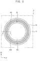
- FIG. 5 is a partially enlarged plan view showing an 'A' region of the OLED device in FIG. 2 .
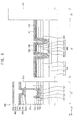
- FIG. 6 is a sectional view taken along line I-I' of the OLED device in FIG. 5 .
- the OLED device 100 may include a substrate 110, an undercut structure 400, a semiconductor element 250, a planarization layer 270, a light emitting structure 200, a pixel defining layer 310, a thin film encapsulation structure 450, and a functional module 700.
- the substrate 110 may include a first organic film layer 111, a first barrier layer 112, a second organic film layer 113, and a second barrier layer 114.
- the substrate 110 may also be divided into the display region 10, the opening region 20, the peripheral region 30, and the pad region 40.
- the undercut structure 400 may include a sacrificial metal pattern 405, a first insulating layer pattern 410, a second insulating layer pattern 420, a third insulating layer pattern 430, and a fourth insulating layer pattern 440
- the semiconductor element 250 may include an active layer 130, a gate insulating layer 150, a gate electrode 170, an insulating interlayer 190, a source electrode 210, and a drain electrode 230.
- the light emitting structure 200 may include a lower electrode 290, a light emitting layer 330, and an upper electrode 340
- the thin film encapsulation structure 450 may include a first thin encapsulation layer 451, a second thin encapsulation layer 452, and a third thin encapsulation layer 453.
- the substrate 110 may further include a groove 930 formed in the peripheral region 30, and the undercut structure 400 may be disposed inside the groove 930 and spaced apart from an inner wall of the groove 930.
- each of the light emitting layer 330 and the upper electrode 340 may be spaced apart, inside the groove 930, by the undercut structure 400.
- each of the light emitting layer 330 and the upper electrode 340 may be short-circuited by the undercut structure 400 inside the groove 930.
- the OLED device 100 includes the light emitting layer 330 and the upper electrode 340 that are short-circuited by the undercut structure 400 inside the groove 930, such that moisture, humidity and the like may be prevented from permeating or penetrating into the semiconductor element 250 and the light emitting structure 200.
- the substrate 110 may further include the opening 910 formed in the opening region 20, and the functional module 700 may be disposed in the opening 910 (see FIG. 16 ).
- the first organic film layer 111 may be provided.
- the first organic film layer 111 may include a flexible organic material.
- the first organic film layer 111 may include a random copolymer or a block copolymer.
- the first organic film layer 111 may have a high transparency, a low coefficient of thermal expansion, and a high glass transition temperature. Since the first organic film layer 111 contains an imide group, heat resistance, chemical resistance, abrasion resistance, and electrical characteristics may be high.
- the first organic film layer 111 may include polyimide.
- the first barrier layer 112 may be entirely disposed on the first organic film layer 111.
- the first barrier layer 112 may block moisture permeating or penetrating through the first organic film layer 111.
- the first barrier layer 112 may include a flexible inorganic material.
- the first barrier layer 112 may include silicon oxide, silicon nitride, or the like.
- the first barrier layer 112 may include silicon oxide (SiO), silicon nitride (SiN), silicon oxynitride (SiON), silicon oxycarbide (SiOC), silicon carbonitride (SiCN), aluminum oxide (AIO), aluminum nitride (AIN), tantalum oxide (TaO), hafnium oxide (HfO), zirconium oxide (ZrO), titanium oxide (TiO), and the like.
- the second organic film layer 113 may be disposed on (e.g., directly on) the first barrier layer 112.
- the second organic film layer 113 may have a first opening 701 in the peripheral region 30 (see FIG. 11 ).
- the first opening 701 may expose an upper surface of the first barrier layer 112 located in the peripheral region 30.
- the second organic film layer 113 may include a flexible organic material.
- the second organic film layer 113 may include a random copolymer or a block copolymer.
- the second organic film layer 113 may include polyimide.
- a part of the second organic film layer 113 located in the peripheral region 30 may be partially removed, so that a trench is formed in the second organic film layer 113 located in the peripheral region 30 (e.g., the second organic film layer 113 may include a trench in the peripheral region 30 that does not extend completely through the second organic film layer 113).
- the upper surface of the first barrier layer 112 located in the peripheral region 30 might not be exposed.
- the second barrier layer 114 may be disposed on (e.g., directly on) the second organic film layer 113.
- the second barrier layer 114 may have a second opening 702 that overlaps the first opening 701 in the peripheral region 30.
- the second opening 702 of the second barrier layer 114 may expose the upper surface of the first barrier layer 112 located in the peripheral region 30.
- the first opening 701 and the second opening 702 may be defined as a groove 930 in the substrate 110 (see FIG. 11 ).
- the groove 930 may have a hollow circular shape surrounding the opening 910 of the substrate 110 viewed from the top.
- the second barrier layer 114 may block or at least mitigate against moisture permeating or penetrating through the second organic film layer 113.
- the second barrier layer 114 may include a flexible inorganic material.
- the second barrier layer 114 may include silicon oxide, silicon nitride, or the like.
- the substrate 110 including the first organic film layer 111, the first barrier layer 112, the second organic film layer 113, and the second barrier layer 114 may be protected against moisture.
- the substrate 110 has been described as having four layers, the configuration of embodiments of the present disclosure is not limited thereto.
- the substrate 110 may include a single layer or at least two layers.
- a buffer layer may be disposed on (e.g., directly on) the substrate 110 (such as the second barrier layer 114).
- the buffer layer may be entirely disposed in the display region 10 and the peripheral region 30 on the substrate 110, and the buffer layer may have an opening overlapping the groove 930 of the substrate 110.
- the buffer layer may prevent metal atoms or impurities from diffusing from the substrate 110 to the semiconductor element 250 and the light emitting structure 200, and enable a substantially uniform active layer to be obtained by adjusting the rate of heat transfer during a crystallization process to form the active layer.
- the buffer layer may serve to improve the flatness of the surface of the substrate 110.
- at least two buffer layers may be provided on the substrate 110, or the buffer layer might not be provided.
- the buffer layer may include an organic material or an inorganic material.
- the active layer 130 may be disposed in the display region 10 on the substrate 110.
- the active layer 130 may include an oxide semiconductor, an inorganic semiconductor (such as amorphous silicon and poly silicon), an organic semiconductor, or the like.
- the active layer 130 may have source and drain regions.
- the gate insulating layer 150 may be disposed on the active layer 130.
- the gate insulating layer 150 may cover the active layer 130 in the display region 10 on the substrate 110, extend in a direction from the display region 10 to the opening region 20 (such as the first direction D1), and be disposed in the peripheral region 30 on the substrate 110.
- the gate insulating layer 150 may have a third opening 703 (see FIGS. 9-11 ) that overlaps the groove 930 of the substrate 110 in the peripheral region 30.
- the gate insulating layer 150 may expose the upper surface of the first barrier layer 112 located in the peripheral region 30 through the third opening 703 (see FIG. 11 ).
- the gate insulating layer 150 may sufficiently cover the active layer 130 in the display region 10 on the substrate 110, and have a substantially flat upper surface without generating a step around the active layer 130.
- the gate insulating layer 150 may cover the active layer 130 in the display region 10 on the substrate 110, and be disposed to have a uniform thickness along a profile of the active layer 130 such that a step is formed around the active layer 130.
- the gate insulating layer 150 may include a silicon compound, metal oxide, or the like.
- the gate insulating layer 150 may have a multi-layer structure including a plurality of insulating layers.
- the insulating layers may have different thicknesses or include different materials.
- the gate electrode 170 may be disposed in the display region 10 on the gate insulating layer 150.
- the gate electrode 170 may be disposed on a portion of the gate insulating layer 150 under which the active layer 130 is located.
- the gate electrode 170 may include a metal, an alloy, a metal nitride, a conductive metal oxide, a transparent conductive material, or the like. These may be used alone or in combination with each other.
- the gate electrode 170 may include a multi-layer structure including a plurality of layers.
- the insulating interlayer 190 may be disposed on (e.g., directly on) the gate electrode 170.
- the insulating interlayer 190 may cover the gate electrode 170 in the display region 10 on the substrate 110, extend in the first direction D1, and be disposed in the peripheral region 30 on the substrate 110.
- the insulating interlayer 190 may have a fourth opening 704 (see FIGS. 9-11 ) that overlaps the third opening 703 in the peripheral region 30.
- the insulating interlayer 190 may expose the upper surface of the first barrier layer 112 located in the peripheral region 30 through the fourth opening 704 (see FIG. 11 ).
- the insulating interlayer 190 may sufficiently cover the gate electrode 170 in the display region 10 on the gate insulating layer 150, and have a substantially flat upper surface without generating a step around the gate electrode 170.
- the insulating interlayer 190 may cover the gate electrode 170 in the display region 10 on the gate insulating layer 150, and be disposed to have a uniform thickness along a profile of the gate electrode 170 such that a step is formed around the gate electrode 170.
- the insulating interlayer 190 may include silicon compound, metal oxide, or the like.
- the insulating interlayer 190 may have a multi-layer structure including a plurality of insulating layers.
- the insulating layers may have different thicknesses or include different materials.
- the source electrode 210 and the drain electrode 230 may be disposed in the display region 10 on the insulating interlayer 190.
- the source electrode 210 may be connected to the source region of the active layer 130 through a contact hole formed by removing a first portion of the gate insulating layer 150 and the insulating interlayer 190
- the drain electrode 230 may be connected to the drain region of the active layer 130 through a contact hole formed by removing a second portion of the gate insulating layer 150 and the insulating interlayer 190.
- the source electrode 210 and the drain electrode 230 each may include a metal, an alloy, a metal nitride, a conductive metal oxide, a transparent conductive material, or the like. These may be used alone or in combination with each other.
- the source electrode 210 and the drain electrode 230 each may have a multi-layer structure including a plurality of layers.
- the semiconductor element 250 including the active layer 130, the gate insulating layer 150, the gate electrode 170, the insulating interlayer 190, the source electrode 210, and the drain electrode 230 may be disposed between the substrate 110 and the light emitting structure 200.
- the semiconductor element 250 has been described as having an upper gate structure, the configuration of embodiments of the present invention is not limited thereto.
- the semiconductor element 250 may have a lower gate structure, a double gate structure, or the like.
- the OLED device 100 is described as including one semiconductor element, the configuration of embodiments of the present invention is not limited thereto.
- the OLED device 100 may include at least one semiconductor element and at least one storage capacitor.
- the sacrificial metal pattern 405 may be disposed inside the groove 930 of the substrate 110.
- the sacrificial metal pattern 405 may be disposed on the upper surface of the first barrier layer 112 exposed through the first opening 701 of the second organic film layer 113, the second opening 702 of the second barrier layer 114, the third opening 703 of the gate insulating layer 150, and the fourth opening 704 of the first insulating interlayer 190.
- the sacrificial metal pattern 405 may be disposed on the first organic film layer 111, the second organic film layer 113, the second barrier layer 114, or the gate insulating layer 150.
- the sacrificial metal pattern 405 may have a first width W1, and may be spaced apart from an inner wall of the groove 930 (see FIG. 11 ). In addition, the sacrificial metal pattern 405 may be spaced apart from the light emitting layer 330 and the upper electrode 340 disposed in the groove 930 (or the peripheral region 30). In other words, the sacrificial metal pattern 405 might not be in direct contact with the light emitting layer 330 and the upper electrode 340.
- the top surface of the sacrificial metal pattern 405 may be in contact with the first insulating layer pattern 410, the bottom surface of the sacrificial metal pattern 405 may be in contact with the first barrier layer 112, and both side surfaces of the sacrificial metal pattern 405 may be in direct contact with the first thin-film encapsulation layer 451 (see FIG. 14 ).
- the sacrificial metal pattern 405 may include a metal, an alloy, a metal nitride, a conductive metal oxide, a transparent conductive material, or the like.
- the sacrificial metal pattern 405 may include gold (Au), silver (Ag), aluminum (Al), tungsten (W), copper (Cu), platinum (Pt), nickel (Ni), titanium (Ti), palladium (Pd), magnesium (Mg), calcium (Ca), lithium (Li), chromium (Cr), tantalum (Ta), molybdenum (Mo), scandium (Sc), neodymium (AIN), iridium (Ir), an alloy containing aluminum, aluminum nitride (AIN), an alloy containing silver, tungsten nitride (WN), an alloy containing copper, an alloy containing molybdenum, titanium nitride (TiN), tantalum nitride (TaN), strontium ruthenium oxide (SrRuO
- the sacrificial metal pattern 405 may include a material etched by an etchant used to pattern the lower electrode 290 (such as an etchant used in the process of selectively etching a preliminary lower electrode to form the lower electrode).
- the sacrificial metal pattern 405 may be composed of molybdenum.
- the sacrificial metal pattern 405 may have a multi-layer structure including a plurality of layers.
- the first insulating layer pattern 410 may be disposed on (e.g., directly on) the sacrificial metal pattern 405.
- the first insulating layer pattern 410 may be disposed inside the groove 930.
- the first insulating layer pattern 410 may have a second width W2 greater than the first width W1 of the sacrificial metal pattern 405, and may be spaced apart from an inner wall of the groove 930 (see FIG. 11 ).
- the first insulating layer pattern 410 may be located at the same layer of the display device as the second organic film layer 113.
- the first insulating layer pattern 410 may include a flexible organic material.
- the first insulating layer pattern 410 may include a random copolymer or a block copolymer.
- the first insulating layer pattern 410 may include polyimide.
- the second insulating layer pattern 420 may be disposed on (e.g., directly on) the first insulating layer pattern 410.
- the second insulating layer pattern 420 may be disposed inside the groove 930.
- the width of the second insulation layer pattern 420 may be greater than the first width W1 of the sacrificial metal pattern 405, and may be spaced apart from an inner wall of the groove 930 (see FIG. 11 ).
- the second insulating layer pattern 420 may be located at the same layer of the display device as the second barrier layer 114.
- the width of the second insulating layer pattern 420 may be equal to or smaller than the first width W1 of the sacrificial metal pattern 405.
- the second insulating layer pattern 420 may include a flexible inorganic material.
- the second insulating layer pattern 420 may include silicon oxide, silicon nitride, or the like.
- the third insulating layer pattern 430 may be disposed on (e.g., directly on) the second insulating layer pattern 420.
- the third insulating layer pattern 430 may be disposed inside the third opening 703.
- the width of the third insulating layer pattern 430 may be greater than the first width W1 of the sacrificial metal pattern 405, and may be spaced apart from an inner wall of the third opening 703 (see FIG. 11 ).
- the third insulating layer pattern 430 may be located at the same layer of the display device as the gate insulating layer 150.
- the width of the third insulating layer pattern 430 may be equal to or smaller than the first width W1 of the sacrificial metal pattern 405.
- the third insulating layer pattern 430 may include silicon compound, metal oxide, or the like.
- the fourth insulating layer pattern 440 may be disposed on (e.g., directly on) the third insulating layer pattern 430.
- the fourth insulating layer pattern 440 may be disposed inside the fourth opening 704.
- a width of the fourth insulating layer pattern 440 may be greater than the first width W1 of the sacrificial metal pattern 405, and may be spaced apart from an inner wall of the fourth opening 704 (see FIG. 11 ).
- the fourth insulating layer pattern 440 may be located at the same layer of the display device as the insulating interlayer 190.
- the width of the fourth insulating layer pattern 440 may be equal to or smaller than the first width W1 of the sacrificial metal pattern 405.
- the fourth insulating layer pattern 440 may include silicon compound, metal oxide, or the like.
- the undercut structure 400 which includes the sacrificial metal pattern 405, the first insulating layer pattern 410, the second insulating layer pattern 420, the third insulating layer pattern 430, and the fourth insulating layer pattern 440, may be disposed inside the groove 930.
- the undercut structure 400 may also have a hollow circular shape surrounding the opening 910 viewed from the top (e.g., in plan view) (see FIG. 5 ).
- the groove 930 may have an undercut shape (e.g., the groove 930 extends under a portion of the first insulating layer pattern 410).
- the groove 930 (such as the first opening 701 and the second opening 702), the third opening 703, the fourth opening 704, and the undercut structure 400 may function as a shielding pattern to shield the moisture and/or humidity from being permeated from or penetrating from the opening region 20 into the display region 10.
- a plurality of the shielding patterns may be formed between the groove 930 and the functional module 700, and the shielding patterns may be formed between the light emitting structure 200, which is located adjacent to a boundary between the display region 10 and the peripheral region 30, and the groove 930.
- the planarization layer 270 may be disposed on the insulating interlayer 190, the source electrode 210, and the drain electrode 230.
- the planarization layer 270 may cover, in the display region 10, the source electrode 210 and the drain electrode 230 on the insulating interlayer 190, and the planarization layer 270 might not be disposed in the peripheral region 30.
- the planarization layer 270 may be disposed only in the display region 10 on the insulating interlayer 190.
- the planarization layer 270 may have a relatively large thickness in the display region 10.
- the planarization layer 270 may have a substantially planarized upper surface, and a planarization process may be added with respect to the planarization layer 270 to implement the above planarized upper surface of the planarization layer 270.
- the planarization layer 270 may be disposed to have a uniform thickness along profiles of the source electrode 210 and the drain electrode 230 in the display region 10 on the insulating interlayer 190 such that one or more steps are formed.
- the planarization layer 270 may be formed of an organic material or an inorganic material.
- the planarization layer 270 may include photoresist, polyacryl-based resin, polyimide-based resin, polyamide-based resin, siloxane-based resin, acryl-based resin, and epoxy-based resin.
- the lower electrode 290 may be disposed in the display region 10 on (e.g., directly on) the planarization layer 270.
- the lower electrode 290 may be connected to the drain electrode 230 through a contact hole formed by removing a part of the planarization layer 270, and the lower electrode 290 may be electrically connected to the semiconductor element 250.
- the lower electrode 290 may include a metal, an alloy, a metal nitride, a conductive metal oxide, a transparent conductive material, or the like. These may be used alone or in combination with each other.
- the lower electrode 290 may have a multi-layer structure including a plurality of layers.
- the lower electrode 290 may have a multi-layer structure in which indium tin oxide, silver, and indium tin oxide are sequentially stacked.
- the pixel defining layer 310 may be disposed in the display region 10 on (e.g., directly on) the planarization layer 270, and might not be disposed in the peripheral region 30. In other words, the pixel defining layer 310 may be disposed only in the display region 10 on the planarization layer 270. For example, the pixel defining layer 310 may expose a part of the upper surface of the lower electrode 290 while covering both side portions of the lower electrode 290.
- the pixel defining layer 310 may be formed of an organic material or an inorganic material. In exemplary embodiments, the pixel defining layer 310 may include an organic material.
- the light emitting layer 330 may be disposed on the pixel defining layer 310 and the lower electrode 290 in the display region 10, may extend in the first direction D1, and may be disposed in the peripheral region 30 on the substrate 110.
- the light emitting layer 330 may be partially disposed inside the groove 930, and may be spaced apart from another portion of the light emitting layer 330 by the undercut structure 400 in the depth direction at a portion where the groove 930 is located (for example, a direction from the second barrier layer 114 to the first organic film layer 111).
- the light emitting layer 330 may be short-circuited by the undercut structure 400 in the peripheral region 30. That is, the light emitting layer 330 may be separated or divided in the peripheral region 30 by the groove 930, the third opening 703, the fourth opening 704 and the undercut structure 400.
- the light emitting layer 330 would be continuously disposed at a portion where the groove 930 is formed, and the light emitting layer 330 could function as a permeation path for moisture and/or humidity.
- a part of the light emitting layer 330 (such as a side end portion of the light emitting layer 330) would be exposed in the opening region 20, and the moisture and/or humidity could permeate into the exposed part of the light emitting layer 330.
- the semiconductor element 250 and the light emitting structure 200 disposed in the display region 10 positioned adjacent to the peripheral region 30 may be damaged by the moisture and/or humidity.
- the light emitting layer 330 may be separated or divided at the inside of the groove 930.
- the light emitting layer 330 is separated or divided at the inside of the groove 930, such that the moisture permeation path of the light emitting layer 330 may be blocked. Accordingly, pixel defects of the OLED device 100 might not occur even when the light emitting layer 330 is disposed in the peripheral region 30.
- the light emitting layer 330 may have a multi-layered structure including an organic light emitting or emissive layer ("EML”), a hole injection layer (“HIL”), a hole transport layer (“HTL”), an electron transport layer (“ETL”), an electron injection layer (“EIL”), and the like.
- EML organic light emitting or emissive layer
- HIL hole injection layer
- HTL hole transport layer
- ETL electron transport layer
- EIL electron injection layer
- the EML, the HIL, the HTL, the ETL and the EIL may be disposed in the peripheral region 30.
- the HIL, the HTL, the ETL and the EIL other than the EML may be disposed in the peripheral region 30.
- the EML of the light emitting layer 330 may be formed using at least one of light emitting materials capable of emitting different color lights (such as red light, green light, and blue light) according to sub-pixels.
- the EML of the light emitting layer 330 may be formed by laminating a plurality of light emitting materials capable of generating different color lights such as red light, green light, and blue light, such that white light may be emitted as a whole.
- a color filter also may be disposed on the light emitting layer 330 disposed on the lower electrode 290.
- the color filter may include at least one of a red color filter, a green color filter, and a blue color filter.
- the color filter may also include a yellow color filter, a cyan color filter, and a magenta color filter.
- the color filter may include photosensitive resin or color photoresist.
- the upper electrode 340 may overlap the light emitting layer 330 in the display region 10, extend in the first direction D1, and be disposed in the peripheral region 30 on the light emitting layer 330.
- the upper electrode 340 may be partially disposed inside the groove 930, and may be spaced apart from another portion of the upper electrode 340 in the depth direction at the portion where the groove 930 is located (e.g., the upper electrode 340 may be separated or divided at the groove 930).
- the upper electrode 340 may be short-circuited by the undercut structure 400 in the peripheral region 30 of the upper electrode 340. That is, a portion of the upper electrode 340 may be separated or divided in the peripheral region 30 by the groove 930, the third opening 703, the fourth opening 704 and the undercut structure 400.
- the upper electrode 340 would be continuously disposed at a portion where the groove 930 is formed, and the upper electrode 340 could function as a permeation path for moisture and/or humidity.
- a part of the upper electrode 340 (such as a side end portion of the upper electrode 340) would be exposed in the opening region 20, and the moisture and/or humidity could permeate into the exposed part of the upper electrode 340.
- the semiconductor element 250 and the light emitting structure 200 disposed in the display region 10 positioned adjacent to the peripheral region 30 may be damaged by the moisture and/or humidity.
- the upper electrode 340 may be separated or divided at the groove 930.
- the upper electrode 340 is separated or divided at the inside of the groove 930, such that the moisture permeation path of the upper electrode 340 may be blocked. Accordingly, pixel defects of the OLED device 100 might not occur even when the upper electrode 340 is disposed in the peripheral region 30.
- the upper electrode 340 may include a metal, an alloy, a metal nitride, a conductive metal oxide, a transparent conductive material, or the like. These may be used alone or in combination with each other. In other exemplary embodiments, the upper electrode 340 may have a multi-layer structure including a plurality of layers.
- the light emitting structure 200 including the lower electrode 290, the light emitting layer 330, and the upper electrode 340 may be protected against moisture.
- a capping layer (not shown) may be disposed on the upper electrode 340.
- the capping layer may overlap the upper electrode 340 in the display region 10, extend in the first direction D1, and be disposed in the peripheral region 30 on the upper electrode 340.
- the capping layer may be partially disposed inside the groove 930, and may be spaced apart from another portion of the capping layer in the depth direction at the portion where the groove 930 is located.
- the capping layer may be short-circuited by the undercut structure 400 in the peripheral region 30. That is, the capping layer may be separated or divided at the peripheral region 30 by the groove 930, the third opening 703, the fourth opening 704 and the undercut structure 400.
- the capping layer would be continuous at the portion where the groove 930 is formed, and the capping layer could function as a permeation path for moisture and/or humidity.
- a part of the capping layer (such as a side end portion of the capping layer) would be exposed in the opening region 20, and the moisture and/or humidity could permeate into the exposed part of the capping layer.
- the semiconductor element 250 and the light emitting structure 200 disposed in the display region 10 positioned adjacent to the peripheral region 30 may be damaged by the moisture and/or humidity.
- the capping layer may be separated or divided at the groove 930. That is, the capping layer is separated or divided at the inside of the groove 930, such that the moisture permeation path of the capping layer may be blocked. Accordingly, pixel defects of the OLED device 100 might not occur even when the capping layer is disposed in the peripheral region 30.
- the capping layer may protect the light emitting structure 200, and include an organic material or an inorganic material.
- the capping layer may include an organic material such as a triamine derivative, an arylenediamine derivative, 4,4'-N,N'-dicarbazole-biphenyl (4,4'-bis(N-carbazolyl)-1,1'-biphenyl (CBP)), and tris-8-hydroxyquinoline aluminum (Alq3).
- the first thin film encapsulation layer 451 may be disposed in the display region 10 and the peripheral region 30 on the upper electrode 340.
- the first thin film encapsulation layer 451 may cover the upper electrode 340 in the display region 10, be disposed to have a uniform thickness along a profile of the upper electrode 340, and extend to the peripheral region 30.
- the first thin film encapsulation layer 451 may be disposed along the profile of the upper electrode 340 in the peripheral region 30. In other words, the first thin film encapsulation layer 451 may be continuously disposed at the portion where the groove 930 is formed. In exemplary embodiments, the first thin film encapsulation layer 451 may completely cover the groove 930 and the undercut structure 400.
- the first thin film encapsulation layer 451 may be in direct contact with both side portions of the sacrificial metal pattern 405.
- the first thin film encapsulation layer 451 may prevent the light emitting structure 200 from deteriorating due to the permeation of the moisture, oxygen, or the like.
- the first thin film encapsulation layer 451 may also function to protect the light emitting structure 200 from an external impact.
- the first thin film encapsulation layer 451 may include flexible inorganic materials.
- the second thin film encapsulation layer 452 may be disposed in the display region 10 on the first thin film encapsulation layer 451, and the second thin film encapsulation layer 452 may not be disposed in the peripheral region 30. In other words, the second thin film encapsulation layer 452 may be disposed only in the display region 10. Alternatively, the second thin film encapsulation layer 452 may be disposed in a part of the peripheral region 30.
- the second thin film encapsulation layer 452 may improve the flatness of the OLED device 100 and protect the light emitting structure 200.
- the second thin film encapsulation layer 452 may include flexible organic materials.
- the third thin film encapsulation layer 453 may be disposed in the display region 10 on the second thin film encapsulation layer 452 and the peripheral region 30 on the first thin encapsulation layer 451.
- the third thin film encapsulation layer 451 may cover the second thin film encapsulation layer 451 in the display region 10, may be disposed to have a uniform thickness along a profile of the second thin film encapsulation layer 452, and may extend to the peripheral region 30.
- the third thin film encapsulation layer 453 may be disposed along a profile of the first thin encapsulation layer 451 in the peripheral region 30. In other words, the third thin film encapsulation layer 453 may be continuous at the portion where the groove 930 is formed.
- the third thin film encapsulation layer 453 may prevent the light emitting structure 200 from deteriorating due to the permeation of the moisture, oxygen, or the like, together with the first thin film encapsulation layer 451.
- the third thin film encapsulation layer 453 may also function to protect the light emitting structure 200 from the external impact.
- the third thin film encapsulation layer 453 may include flexible inorganic materials.
- the thin film encapsulation structure 450 may include the first thin film encapsulation layer 451, the second thin film encapsulation layer 452, and the third thin film encapsulation layer 453.
- the thin film encapsulation structure 450 may be a five-layer structure laminated with first to fifth thin film encapsulation layers or a seven-layer structure laminated with first to seventh thin film encapsulation layers.
- the functional module 700 may be disposed in the opening region 20.
- the functional module 700 may be in contact with a side surface of the substrate 110, a side surface of the light emitting layer 330, a side surface of the upper electrode 340, a side surface of the first thin film encapsulation layer 451, and a side surface of the third thin encapsulation layer 453 at a boundary between the peripheral region 30 and the opening region 20.
- the functional module 700 may include a camera module, a face recognition sensor module, a pupil recognition sensor module, an acceleration sensor module and a geomagnetism sensor module, a proximity sensor module and an infrared sensor module, an illuminance sensor module, a vibration module, and/or a speaker module.
- the OLED device 100 includes the undercut structure 400 disposed inside the groove 930, so that the OLED device 100 can prevent or at least mitigate against moisture, humidity and the like from permeating into the semiconductor element 250 and the light emitting structure 200 from the peripheral region 30 to the display region 10.
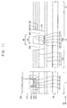
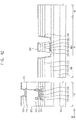
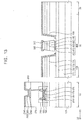
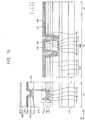
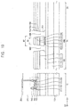
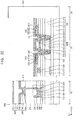
- FIGS. 7 to 17 are sectional views describing a method of manufacturing an OLED device according to exemplary embodiments of the present invention.
- a rigid glass substrate 105 may be provided or obtained.
- a first organic film layer 111 may be formed on the glass substrate 105.
- the first organic film layer 111 may be formed entirely on the glass substrate 105, and may be formed by using a flexible organic material such as polyimide.
- a first barrier layer 112 may be formed entirely on the first organic film layer 111.
- the first barrier layer 112 may block or at least mitigate against moisture permeating or penetrating through the first organic film layer 111.
- the first barrier layer 112 may be formed by using a flexible inorganic material such as silicon oxide and silicon nitride.
- the first barrier layer 112 may include SiO, SiN, SiON, SiOC, SiCN, AIO, AIN, TaO, HfO, ZrO, TiO, and the like.
- a preliminary sacrificial metal pattern 401 may be formed in the peripheral region 30 on the first barrier layer 112.
- the preliminary sacrificial metal pattern 401 may be formed by using a metal, an alloy, a metal nitride, a conductive metal oxide, a transparent conductive material, or the like.
- the preliminary sacrificial metal pattern 401 may include Au, Ag, Al, W, Cu, Pt, Ni, Ti, Pd, Mg, Ca, Li, Cr, Ta, Mo, Sc, AIN, Ir, an alloy containing aluminum, AIN, an alloy containing silver, WN, an alloy containing copper, an alloy containing molybdenum, TiN, TaN, SrRuO, ZnO, ITO, SnO, InO, GaOx, IZO, or the like. These may be used alone or in combination with each other.
- the preliminary sacrificial metal pattern 401 may include a material etched by an etchant used to pattern the lower electrode (such as an etchant used in the process of selectively etching a preliminary lower electrode to form the lower electrode), which will be described later.
- the preliminary sacrificial metal pattern 401 may be composed of molybdenum.
- the preliminary sacrificial metal pattern 401 may have a multi-layer structure including a plurality of layers.
- a second organic film layer 113 may be formed on the first barrier layer 112.
- the second organic film layer 113 may be formed entirely on the first barrier layer 112, and may be formed by using a flexible organic material such as polyimide.
- the second organic film layer 113 may sufficiently cover the preliminary sacrificial metal pattern 401 in the peripheral region 30 on the first barrier layer 112, and may have a substantially flat upper surface without generating a step around the preliminary sacrificial metal pattern 401.
- the second organic film layer 113 may cover the preliminary sacrificial metal pattern 401 in the peripheral region 30 on the first barrier layer 112, and may be formed to have a uniform thickness along a profile of the preliminary sacrificial metal pattern 401 such that a step around the preliminary sacrificial metal pattern 401 is formed.
- a second barrier layer 114 may be formed entirely on the second organic film layer 113.
- the second barrier layer 114 may block or at least mitigate against moisture permeating or penetrating through the second organic film layer 113.
- the second barrier layer 114 may be formed by using a flexible inorganic material such as silicon oxide and silicon nitride.
- a substrate 110 may be formed including the first organic film layer 111, the first barrier layer 112, the second organic film layer 113, and the second barrier layer 114.
- the substrate 110 may be formed on a rigid glass substrate 105 to support the formation of an upper structure (such as the semiconductor element and the light emitting structure).
- an upper structure such as the semiconductor element and the light emitting structure.
- the glass substrate 105 may be removed.
- it may be difficult to directly form the upper structure on the first organic film layer 111, the first barrier layer 112, the second organic film layer 113, and the second barrier layer 114.
- the first organic film layer 111, the first barrier layer 112, the second organic film layer 113, and the second barrier layer 114 may be used as the substrate 110 by using the glass substrate 105 to form the upper structure and then removing the glass substrate 105.
- a buffer layer (not shown) may be formed on the substrate 110.
- the buffer layer may be formed entirely on the substrate.
- the buffer layer may prevent metal atoms or impurities from being diffused from the substrate 110, and may enable a substantially uniform active layer to be obtained by adjusting the rate of heat transfer during a crystallization process to form the active layer.
- the buffer layer may serve to improve the flatness of the surface of the substrate 110.
- at least two buffer layers may be provided on the substrate 110, or the buffer layer might not be formed.
- the buffer layer may be formed by using an organic material or an inorganic material.
- An active layer 130 may be formed in the display region 10 on the substrate 110.
- the active layer 130 may be formed by using an oxide semiconductor, an inorganic semiconductor, an organic semiconductor, or the like.
- the active layer 130 may have source and drain regions.
- a gate insulating layer 150 may be formed on the active layer 130.
- the gate insulating layer 150 may cover the active layer 130 in the display region 10 on the substrate 110, and extend in the first direction D1, which is the direction from the display region 10 to the opening region 20 in the gate insulating layer 150.
- the gate insulating layer 150 may be formed entirely on the substrate 110.
- the gate insulating layer 150 may sufficiently cover the active layer 130 on the substrate 110, and have a substantially flat upper surface without generating a step around the active layer 130.
- the gate insulating layer 150 may cover the active layer 130 on the substrate 110, and may be formed to have a uniform thickness along the profile of the active layer 130 such that a step around the active layer 130 is formed.
- the gate insulating layer 150 may be formed by using silicon compound, metal oxide, or the like.
- the gate insulating layer 150 may have a multi-layer structure including a plurality of insulating layers.
- the insulating layers may have different thicknesses or include different insulating materials.
- a gate electrode 170 may be formed in the display region 10 on the gate insulating layer 150.
- the gate electrode 170 may be formed on a portion of the gate insulating layer 150 below which the active layer 130 is located.
- the gate electrode 170 may be formed by using a metal, an alloy, a metal nitride, a conductive metal oxide, a transparent conductive material, or the like. These may be used alone or in combination with each other.
- the gate electrode 170 may include a multi-layer structure including a plurality of layers.
- An insulating interlayer 190 may be formed on the gate electrode 170.
- the insulating interlayer 190 may cover the gate electrode 170 in the display region 10 on the gate insulating layer 150, and may extend in the first direction D1 on the gate insulating layer 150.
- the insulating interlayer 190 may be formed entirely on the gate insulating layer 150.
- the insulating interlayer 190 may sufficiently cover the gate electrode 170 on the gate insulating layer 150, and may have a substantially flat upper surface without generating a step around the gate electrode 170.
- the insulating interlayer 190 may cover the gate electrode 170 on the gate insulating layer 150, and may be formed to have a uniform thickness along the profile of the gate electrode 170 such that a step is formed around the gate electrode 170.
- the insulating interlayer 190 may be formed by using silicon compound, metal oxide, or the like.
- the insulating interlayer 190 may have a multi-layer structure including a plurality of insulating layers.
- the insulating layers may have different thicknesses or include different insulating materials.
- a first contact hole 212 exposing the source region of the active layer 130 may be formed by removing first portions of the gate insulating layer 150 and the insulating interlayer 190, and a second contact hole 232 exposing the drain region of the active layer 130 may be formed by removing second portions of the gate insulating layer 150 and the insulating interlayer 190.
- a third contact hole 222 exposing a third portion of the preliminary sacrificial metal pattern 401 may be formed by removing the first portions of the insulating interlayer 190, the gate insulating layer 150, the second barrier layer 114, and the second organic film layer 113
- a fourth contact hole 242 exposing a fourth portion of the preliminary sacrificial metal pattern 401 may be formed by removing second portions of the insulating interlayer 190, the gate insulating layer 150, the second barrier layer 114, and the second organic film layer 113.
- the first contact hole 212, the second contact hole 232, the third contact hole 222, and the fourth contact hole 242 may be formed at the same time.
- patterned photoresists such as photoresists having different heights
- an etching process is performed so that the first contact hole 212, the second contact hole 232, the third contact hole 222, and the fourth contact hole 242 may be formed in the same process.
- an additional etching process is performed, so that the second barrier layer 114 and the second organic film layer 113 may be removed from the third and fourth portions of the sacrificial metal pattern 401, and the third contact hole 222 and the fourth contact hole 242 may be formed at the same time.
- the first insulating layer pattern 410, the second insulating layer pattern 420, the third insulating layer pattern 430, and the fourth insulating layer pattern 440 may be defined on the preliminary sacrificial metal pattern 401.
- a space formed through the third contact hole 222 and the fourth contact hole 242 in the second organic film layer 113 is defined as the first opening 701
- a space formed through the third contact hole 222 and the fourth contact hole 242 in the second barrier layer 114 is defined as the second opening 702
- a space formed through the third contact hole 222 and the fourth contact hole 242 in the gate insulating layer 150 is defined as the third opening 703
- a space formed through the third contact hole 222 and the fourth contact hole 242 in the insulating interlayer 190 is defined as the fourth opening 704.
- a source electrode 210 may be formed to be connected to the source region of the active layer 130 through the first contact hole 212, and a drain electrode 230 may be formed to be connected to the drain region of the active layer 130 through the second contact hole 232.
- the source electrode 210 and the drain electrode 230 each may be formed by using a metal, an alloy, a metal nitride, a conductive metal oxide, a transparent conductive material, or the like. These may be used alone or in combination with each other.
- the source electrode 210 and the drain electrode 230 may each have a multi-layer structure including a plurality of layers.
- a semiconductor element 250 may be formed including the active layer 130, the gate insulating layer 150, the gate electrode 170, the insulating interlayer 190, the source electrode 210, and the drain electrode 230.
- a planarization layer 270 may be formed on the insulating interlayer 190, the source electrode 210, and the drain electrode 230.
- the planarization layer 270 may cover the source electrode 210 and the drain electrode 230 in the display region 10 on the insulating interlayer 190, and may not be formed in the peripheral region 30.
- the planarization layer 270 may be formed only in the display region 10 on the insulating interlayer 190.
- the planarization layer 270 may have a relatively high thickness in the display region 10.
- the planarization layer 270 may have a substantially planarized upper surface, and a planarization process may be performed with respect to the planarization layer 270 to achieve the above planarized upper surface of the planarization layer 270.
- the planarization layer 270 may be formed to have a uniform thickness along profiles of the source electrode 210 and the drain electrode 230 in the display region 10 on the insulating interlayer 190.
- the planarization layer 270 may be formed by using an organic material such as photoresist, polyacryl-based resin, polyimide-based resin, polyamide-based resin, siloxane-based resin, acryl-based resin, and epoxy-based resin.
- a lower electrode 290 may be formed in the display region 10 on the planarization layer 270.
- the lower electrode 290 may be connected to the drain electrode 230 through a contact hole formed by removing a part of the planarization layer 270, and the lower electrode 290 may be electrically connected to the semiconductor element 250.
- the lower electrode 290 may be formed by using a metal, an alloy, a metal nitride, a conductive metal oxide, a transparent conductive material, or the like. These may be used alone or in combination with each other.
- the lower electrode 290 may have a multi-layer structure including a plurality of layers.
- the lower electrode 290 may have a multi-layer structure in which indium tin oxide, silver, and indium tin oxide are sequentially stacked.
- a preliminary electrode layer may be formed entirely on the substrate 110, and then the preliminary electrode layer may be etched so that the lower electrode 290 may be formed.
- the above etching process may proceed using a wet etching process, in which an etchant used in the wet etching process may be a mixed solution including phosphoric acid, acetic acid, nitric acid, or the like.
- the etchant may be composed of phosphoric acetic nitric acid.
- the etchant may etch the preliminary electrode layer and simultaneously etch a part of the preliminary sacrificial metal pattern 401 (such as both side portions of the preliminary sacrificial metal pattern 401).
- the etchant may simultaneously etch the preliminary electrode layer and the preliminary sacrificial metal pattern 401, so that the lower electrode 290 and the sacrificial metal pattern 405 may be formed simultaneously.
- the first opening 701 and the second opening 702 together define the groove 930 in the substrate 110.
- the sacrificial metal pattern 405 having the first width W1 smaller than the width of the preliminary sacrificial metal pattern 401 may be formed, and the sacrificial metal pattern 405 is formed under the first insulating layer pattern 410 having the second width W2 greater than the first width W1, so that an undercut shape may be generated (e.g., the sacrificial metal pattern 405 having the first width W1 smaller than the second width W2 of the first insulating layer pattern 410 is formed under the first insulating layer pattern 410).
- an undercut structure 400 may be formed which includes the sacrificial metal pattern 405, the first insulating layer pattern 410, the second insulating layer pattern 420, the third insulating layer pattern 430 and the fourth insulating layer pattern 440.
- a groove 930 (such as the first opening 701 and the second opening 702), the third opening 703, the fourth opening 704, and the undercut structure 400 may function as a shielding pattern to shield moisture and/or humidity from permeating or penetrating into the display region 10 from the opening region 20.
- the pixel defining layer 310 may be formed in the display region 10 on the planarization layer 270, and may not be formed in the peripheral region 30. In other words, the pixel defining layer 310 may be formed only in the display region 10 on the planarization layer 270. For example, the pixel defining layer 310 may expose a part of the upper surface of the lower electrode 290 while covering both side portions of the lower electrode 290.
- the pixel defining layer 310 may be formed by using an organic material.
- a light emitting layer 330 may be formed on the pixel defining layer 310 and the lower electrode 290 in the display region 10, extend in the first direction D1, and be formed in the peripheral region 30 on the substrate 110.
- the light emitting layer 330 may be partially formed inside the groove 930, and may be spaced apart from another portion of the light emitting layer 330 by the undercut structure 400 in the depth direction at a portion where the groove 930 is located (for example, from the second barrier layer 114 to the first organic film layer 111).
- the light emitting layer 330 may be short-circuited by the undercut structure 400 in the peripheral region 30. That is, the light emitting layer 330 may be separated or divided in the peripheral region 30 by the groove 930, the third opening 703, the fourth opening 704, and the undercut structure 400.
- the light emitting layer 330 may have a multilayer structure including an EML, an HIL, an HTL, an ETL, and an EIL.
- the EML, the HIL, the HTL, the ETL and the EIL may be formed in the peripheral region 30.
- the HIL, the HTL, the ETL and the EIL other than the EML may be formed in the peripheral region 30.
- the EML of the light emitting layer 330 may be formed using at least one of light emitting materials capable of emitting different color lights (such as red light, green light, and blue light) according to sub-pixels.
- the EML of the light emitting layer 330 may be formed by laminating a plurality of light emitting materials capable of generating different color lights such as red light, green light, and blue light, such that white light may be emitted as a whole.
- a color filter may also be formed on the light emitting layer 330 disposed on the lower electrode 290.
- the color filter may include at least one of a red color filter, a green color filter, or a blue color filter.
- the color filter may also include a yellow color filter, a cyan color filter, or a magenta color filter.
- the color filter may be formed by using photosensitive resin or color photoresist.
- an upper electrode 340 may overlap the light emitting layer 330 in the display region 10, extend in the first direction D1, and be formed in the peripheral region 30 on the light emitting layer 330.
- the upper electrode 340 may be partially formed inside the groove 930, and spaced apart from another portion of the upper electrode 340 in the depth direction at the portion where the groove 930 is located.
- the upper electrode 340 may be short-circuited by the undercut structure 400 in the peripheral region 30 of the upper electrode 340. That is, the upper electrode 340 may be separated or divided in peripheral region 30 by the groove 930, the third opening 703, the fourth opening 704, and the undercut structure 400.
- the upper electrode 340 may be formed by using a metal, an alloy, a metal nitride, a conductive metal oxide, a transparent conductive material, or the like. These may be used alone or in combination with each other. In other exemplary embodiments, the upper electrode 340 may have a multi-layer structure including a plurality of layers.
- a light emitting structure 200 may be formed including the lower electrode 290, the light emitting layer 330, and the upper electrode 340.
- a capping layer (not shown) may be formed on the upper electrode 340.
- the capping layer may overlap the upper electrode 340 in the display region 10, extend in the first direction D1, and be formed in the peripheral region 30 on the upper electrode 340.
- the capping layer may be partially formed inside the groove 930, and spaced apart from another portion of the capping layer in the depth direction at the portion where the groove 930 is located.
- the capping layer may be short-circuited by the undercut structure 400 in the peripheral region 30. That is, the capping layer may be separated or divided in the peripheral region 30 by the groove 930, the third opening 703, the fourth opening 704, and the undercut structure 400.
- the capping layer may protect the light emitting structure 200, and may be formed by using an organic material such as a triamine derivative, an arylenediamine derivative, 4,4'-N,N'-dicarbazole-biphenyl, and tris-8-hydroxyquinoline aluminum.
- a first thin film encapsulation layer 451 may be formed in the display region 10 and the peripheral region 30 on the upper electrode 340.
- the first thin film encapsulation layer 451 may cover the upper electrode 340 in the display region 10, be formed to have a uniform thickness along the profile of the upper electrode 340, and extend to the peripheral region 30.
- the first thin film encapsulation layer 451 may be formed along the profile of the upper electrode 340 in the peripheral region 30. In other words, the first thin film encapsulation layer 451 may be continuously formed along the portion of the peripheral region 30 where the groove 930 is formed. In exemplary embodiments, the first thin film encapsulation layer 451 may completely cover the groove 930 and the undercut structure 400.
- the first thin film encapsulation layer 451 may be in direct contact with both side portions of the sacrificial metal pattern 405.
- the first thin film encapsulation layer 451 may prevent the light emitting structure 200 from deteriorating due to the permeation of the moisture, oxygen, or the like.
- the first thin film encapsulation layer 451 may also function to protect the light emitting structure 200 from an external impact.
- the first thin film encapsulation layer 451 may be formed by using flexible inorganic materials.
- a second thin film encapsulation layer 452 may be formed in the display region 10 on the first thin film encapsulation layer 451, and the second thin film encapsulation layer 452 may not be formed in the peripheral region 30. In other words, the second thin film encapsulation layer 452 may be formed only in the display region 10. Alternatively, the second thin film encapsulation layer 452 may be formed in a part of the peripheral region 30. The second thin film encapsulation layer 452 may improve the flatness of the OLED device 100 and protect the light emitting structure 200. The second thin film encapsulation layer 452 may be formed by using flexible organic materials.
- a third thin film encapsulation layer 453 may be formed in the display region 10 on the second thin film encapsulation layer 452 and the peripheral region 30 on the first thin encapsulation layer 451.
- the third thin film encapsulation layer 451 may cover the second thin film encapsulation layer 451 in the display region 10, be formed to have a uniform thickness along the profile of the second thin film encapsulation layer 452, and extend to the peripheral region 30.
- the third thin film encapsulation layer 453 may be formed to have a uniform thickness along the profile of the first thin film encapsulation layer 451.
- the third thin film encapsulation layer 453 may be continuously formed along the portion of the peripheral region 30 where the groove 930 is formed.
- the third thin film encapsulation layer 453 may prevent the light emitting structure 200 from deteriorating due to the permeation of the moisture, oxygen, or the like, together with the first thin film encapsulation layer 451.
- the third thin film encapsulation layer 453 may also function to protect the light emitting structure 200 from the external impact.
- the third thin film encapsulation layer 453 may be formed by using flexible inorganic materials.
- a thin film encapsulation structure 450 may be formed including the first thin film encapsulation layer 451, the second thin film encapsulation layer 452, and the third thin film encapsulation layer 453.
- the thin film encapsulation structure 450 may be formed in a five-layer structure laminated with first to fifth thin film encapsulation layers, or a seven-layer structure laminated with first to seventh thin film encapsulation layers.
- a laser may be utilized to irradiate the opening region 20 on the third thin film encapsulation layer 453.
- another etching process may be performed to expose the opening region 20 on the third thin film encapsulation layer 453.
- an opening 910 may be formed in the opening region 20 by the laser irradiation, and the functional module 700 may be formed in the opening 910.
- the functional module 700 may be in contact with a side surface of the substrate 110, a side surface of the light emitting layer 330, a side surface of the upper electrode 340, a side surface of the first thin film encapsulation layer 451, and a side surface of the third thin encapsulation layer 453 at a boundary between the peripheral region 30 and the opening region 20.
- the functional module 700 may include a camera module, a face recognition sensor module, a pupil recognition sensor module, an acceleration sensor module and a geomagnetism sensor module, a proximity sensor module and an infrared sensor module, an illuminance sensor module, a vibration module, and/or a speaker module.
- the functional module 700 may include a camera module, a face recognition sensor module, a pupil recognition sensor module, an acceleration sensor module and a geomagnetism sensor module, a proximity sensor module and an infrared sensor module, an illuminance sensor module, a vibration module, and/or a speaker module.
- FIGS. 18 and 19 are sectional views depicting a method of manufacturing an OLED device according to exemplary embodiments of the present disclosure.
- a first contact hole 1212, a second contact hole 1232, a third contact hole 1222, and a fourth contact hole 1242 may be formed in the display region 10 and the peripheral region 30.
- the first contact hole 1212 and the second contact hole 1232 formed in the display region 10 shown in FIG. 18 may be substantially the same as the first contact hole 212 and the second contact hole 232, respectively, shown in FIG. 9 .
- widths of the third contact holes 1222 and the fourth contact hole 1242 in FIG. 18 may be relatively smaller, respectively.
- both side portions of the preliminary sacrificial metal pattern 401 in FIG. 9 are exposed, both side portions of the preliminary sacrificial metal pattern 402 in FIG. 18 may be covered by the second barrier layer 114.
- a preliminary electrode layer may be formed entirely on the substrate 110, and then the lower electrode 290 may be formed by etching the preliminary electrode layer.
- the above etching process may proceed using a wet etching process in which an etchant used in the wet etching process may be a mixed solution including phosphoric acid, acetic acid, nitric acid, or the like.
- the etchant may be composed of phosphoric acetic nitric acid.
- the etchant may etch the preliminary electrode layer and simultaneously etch a part of the preliminary sacrificial metal pattern 402 (such as both side portions of the preliminary sacrificial metal pattern 402).
- the etchant may simultaneously etch the preliminary electrode layer and the preliminary sacrificial metal pattern 402, so that the lower electrode 290 and the sacrificial metal pattern 405 may be formed simultaneously.
- the first opening 701 and the second opening 702 together define the groove 930 in the substrate 110.
- the second barrier layer 114 may have a shape in which a lower portion thereof is expanded laterally outward.
- the groove 930 may have an undercut shape in which a lower portion thereof is expanded laterally outward.
- FIG. 20 is a sectional view showing an OLED device according to exemplary embodiments of the present invention.
- the OLED device 500 illustrated in FIG. 20 may have substantially the same or similar configuration as the OLED device 100 described with reference to FIGS. 1 to 6 .
- duplicate descriptions for components substantially the same as or similar to the components described with reference to FIGS. 1 to 6 will be omitted.
- the OLED device 500 may include a substrate 110, an undercut structure 1400, a first wire 510, a second wire 520, a third wire 530, a semiconductor element 250, a first sub-undercut structure 515, a second sub-undercut structure 525, a planarization layer 270, a light emitting structure 200, a pixel defining layer 310, a thin film encapsulation structure 450, a functional module 700, and the like.
- the substrate 110 may include a first organic film layer 111, a first barrier layer 112, a second organic film layer 113 and a second barrier layer 114.
- the undercut structure 1400 may include a first sacrificial metal pattern 405, a first insulating layer pattern 410, a second insulating layer pattern 420, a third insulating layer pattern 430, a second sacrificial metal pattern 415, a fourth insulating layer pattern 440, and a fifth insulating layer pattern 460
- the first sub-undercut structure 515 may include a first sub-sacrificial metal pattern 461 and a first sub-insulating layer pattern 411
- the second sub-undercut structure 525 may include a second sub-sacrificial metal pattern 462 and a second sub-insulating layer pattern 412.
- the semiconductor element 250 may include an active layer 130, a gate insulating layer 150, a first gate electrode 170, a second gate electrode 175, a first insulating interlayer 190, a second insulating interlayer 195, a source electrode 210, and a drain electrode 230.
- the light emitting structure 200 may include a lower electrode 290, a light emitting layer 330, and an upper electrode 340
- the thin film encapsulation structure 450 may include a first thin encapsulation layer 451, a second thin encapsulation layer 452, and a third thin encapsulation layer 453.
- the substrate 110 may further include a groove 930 formed in the peripheral region 30, and the undercut structure 1400 may be disposed inside the groove 930 and spaced apart from an inner wall of the groove 930.
- the light emitting layer 330 and the upper electrode 340 may be spaced apart, inside the groove 930, by the undercut structure 1400. In other words, each of the light emitting layer 330 and the upper electrode 340 may be short-circuited by the undercut structure 1400 inside the groove 930.
- the first sub-undercut structure 515 and the second sub-undercut structure 525 are disposed outside the groove 930 (for example, on the upper surface of the first insulating interlayer 190), so that each of the light emitting layer 330 and the upper electrode 340 may be short-circuited.
- the OLED device 500 includes the light emitting layer 330 and the upper electrode 340 short-circuited by the undercut structure 1400 and the first and second sub-undercut structures 515 and 525 inside and outside the groove 930, so that the moisture, humidity and the like may be prevented from permeating into the semiconductor element 250 and the light emitting structure 200.
- the substrate 110 may further include the opening 910 formed in the opening region 20, and the functional module 700 may be disposed in the opening 910.
- the first gate electrode 170 may be disposed in the display region 10 on the gate insulating layer 150.
- the first gate electrode 170 may be disposed on a portion of the gate insulating layer 150 which the active layer 130 is located below.
- the first gate electrode 170 may include a metal, an alloy, a metal nitride, a conductive metal oxide, a transparent conductive material, or the like. These may be used alone or in combination with each other.
- the first gate electrode 170 may be composed of molybdenum.
- the first gate electrode 170 may include a multi-layer structure including a plurality of layers.
- the first insulating interlayer 190 may be disposed on the first gate electrode 170.
- the first insulating interlayer 190 may cover the first gate electrode 170 in the display region 10 on the substrate 110, extend in the first direction D1, and be disposed in the peripheral region 30 on the substrate 110.
- the first insulating interlayer 190 may have a fourth opening 704 that overlaps the third opening 703 in the peripheral region 30.
- the first insulating interlayer 190 may expose the upper surface of the first barrier layer 112 located in the peripheral region 30 through the fourth opening 704.
- the first insulating interlayer 190 may sufficiently cover the first gate electrode 170 in the display region 10 on the gate insulating layer 150, and have a substantially flat upper surface without generating a step around the first gate electrode 170.
- the first insulating interlayer 190 may cover the first gate electrode 170 in the display region 10 on the gate insulating layer 150, and be disposed to have a uniform thickness along a profile of the first gate electrode 170.
- the first insulating interlayer 190 may include silicon compound, metal oxide, or the like.
- the insulating interlayer 190 may have a multi-layer structure including a plurality of insulating layers.
- the insulating layers may have different thicknesses or include different materials.
- the second gate electrode 175 may be disposed in the display region 10 on the first gate insulating layer 190.
- the second gate electrode 175 may be disposed on a portion of the first gate insulating layer 190 which the first gate electrode 170 is located below.
- the second gate electrode 175 may include a metal, an alloy, a metal nitride, a conductive metal oxide, a transparent conductive material, or the like. These may be used alone or in combination with each other.
- the second gate electrode 175 may be composed of molybdenum.
- the second gate electrode 175 may include a multi-layer structure including a plurality of layers.
- the second insulating interlayer 195 may be disposed on the second gate electrode 175.
- the second insulating interlayer 195 may cover the second gate electrode 175 in the display region 10 on the substrate 110, extend in the first direction D1, and be disposed in the peripheral region 30 on the substrate 110.
- the second insulating interlayer 195 may have a fifth opening that overlaps the fourth opening 704 in the peripheral region 30.
- the width of the fifth opening may be greater than the width of the fourth opening 704, and a part of an upper surface of the first insulating interlayer 190 and a part of the upper surface of the first barrier layer 112 located in the peripheral region 30 may be exposed through the fifth opening.
- the second insulating interlayer 195 may sufficiently cover the second gate electrode 175 in the display region 10 on the first insulating interlayer 190, and have a substantially flat upper surface without generating a step around the second gate electrode 175.
- the second insulating interlayer 195 may cover the second gate electrode 175 in the display region 10 on the first insulating interlayer 190, and be disposed to have a uniform thickness along a profile of the second gate electrode 175.
- the second insulating interlayer 195 may include silicon compound, metal oxide, or the like.
- the second insulating interlayer 195 may have a multi-layer structure including a plurality of insulating layers.
- the insulating layers may have different thicknesses or include different materials.
- the source electrode 210 and the drain electrode 230 may be disposed in the display region 10 on the second insulating interlayer 195.
- the source electrode 210 may be connected to the source region of the active layer 130 through a contact hole formed by removing first portions of the gate insulating layer 150, the first insulating interlayer 190, and the second insulating interlayer 195
- the drain electrode 230 may be connected to the drain region of the active layer 130 through a contact hole formed by removing second portions of the gate insulating layer 150, the first insulating interlayer 190, and the second insulating interlayer 195.
- the source electrode 210 and the drain electrode 230 may each include a metal, an alloy, a metal nitride, a conductive metal oxide, a transparent conductive material, or the like. These may be used alone or in combination with each other. In other exemplary embodiments, the source electrode 210 and the drain electrode 230 may each have a multi-layer structure including a plurality of layers.
- the semiconductor element 250 including the active layer 130, the gate insulating layer 150, the first gate electrode 170, the first insulating interlayer 190, the second gate electrode 175, the second insulating interlayer 195, the source electrode 210, and the drain electrode 230 may be disposed between the substrate 110 and the light emitting structure 200.
- the first sacrificial metal pattern 405 may be disposed inside the groove 930 of the substrate 110. In other words, the first sacrificial metal pattern 405 may be disposed on the upper surface of the first barrier layer 112. In exemplary embodiments, the first sacrificial metal pattern 405 may have the first width W1, and be spaced apart from the inner wall of the groove 930. In addition, the sacrificial metal pattern 405 may be spaced apart from the light emitting layer 330 and the upper electrode 340 disposed in the groove 930 (or the peripheral region 30). In other words, the first sacrificial metal pattern 405 might not be in direct contact with the light emitting layer 330 and the upper electrode 340.
- the first sacrificial metal pattern 405 may include a metal, an alloy, a metal nitride, a conductive metal oxide, a transparent conductive material, or the like. These may be used alone or in combination with each other.
- the first sacrificial metal pattern 405 may include a material etched by an etchant used to pattern the lower electrode 290.
- the first sacrificial metal pattern 405 may be composed of molybdenum.
- the first sacrificial metal pattern 405 may have a multi-layer structure including a plurality of layers.
- the first insulating layer pattern 410 may be disposed on the first sacrificial metal pattern 405.
- the first insulating layer pattern 410 may be disposed inside the groove 930.
- the first insulating layer pattern 410 may have a second width W2 greater than the first width W1, and be spaced apart from the inner wall of the groove 930.
- the first insulating layer pattern 410 may be located on the same layer as the second organic film layer 113.
- the first insulating layer pattern 410 may include a flexible organic material.
- the first insulating layer pattern 410 may include a random copolymer or a block copolymer.
- the first insulating layer pattern 410 may include polyimide.
- the second insulating layer pattern 420 may be disposed on the first insulating layer pattern 410.
- the second insulating layer pattern 420 may be disposed inside the groove 930.
- the width of the second insulation layer pattern 420 may be greater than the first width W1, and be spaced apart from the inner wall of the groove 930.
- the second insulating layer pattern 420 may be located on the same layer as the second barrier layer 114.
- the width of the second insulating layer pattern 420 may be equal to or smaller than the first width W1.
- the second insulating layer pattern 420 may include a flexible inorganic material.
- the second insulating layer pattern 420 may include silicon oxide, silicon nitride, or the like.
- the third insulating layer pattern 430 may be disposed on the second insulating layer pattern 420.
- the third insulating layer pattern 430 may be disposed inside the third opening 703.
- the width of the third insulating layer pattern 430 may be greater than the first width W1, and be spaced apart from the inner wall of the third opening 703.
- the third insulating layer pattern 430 may be located on the same layer as the gate insulating layer 150.
- the width of the third insulating layer pattern 430 may be equal to or smaller than the first width W1.
- the third insulating layer pattern 430 may include silicon compound, metal oxide, or the like.
- the second sacrificial metal pattern 415 may be disposed inside the fourth opening 704 of the first insulating interlayer 190. In other words, the second sacrificial metal pattern 415 may be disposed on an upper surface of the third insulating layer pattern 430. In exemplary embodiments, the width of the second sacrificial metal pattern 415 may be smaller than the first width W1, and be spaced apart from the inner wall of the fourth opening 704. In addition, the sacrificial metal pattern 405 may be spaced apart from the light emitting layer 330 and the upper electrode 340 disposed in the groove 930 (or the peripheral region 30). In other words, the second sacrificial metal pattern 415 might not be in direct contact with the light emitting layer 330 and the upper electrode 340.
- the second sacrificial metal pattern 415 may include a metal, an alloy, a metal nitride, a conductive metal oxide, a transparent conductive material, or the like. These may be used alone or in combination with each other.
- the second sacrificial metal pattern 415 may include a material etched by an etchant used to pattern the lower electrode 290, and be formed simultaneously by using the same material in the same layer as the first gate electrode 170.
- the second sacrificial metal pattern 405 may be composed of molybdenum.
- the second sacrificial metal pattern 415 may have a multi-layer structure including a plurality of layers.
- the fourth insulating layer pattern 440 may be disposed on the second sacrificial metal pattern 415.
- the fourth insulating layer pattern 440 may be disposed inside the fourth opening 704.
- the width of the fourth insulating layer pattern 440 may be greater than the width of the second sacrificial metal pattern 415, and be spaced apart from the inner wall of the fourth opening 704.
- the fourth insulating layer pattern 440 may be located on the same layer as the first insulating interlayer 190.
- the fourth insulating layer pattern 440 may include silicon compound, metal oxide, or the like.
- the fifth insulating layer pattern 460 may be disposed on the fourth insulating layer pattern 440.
- the fifth insulating layer pattern 460 may be disposed inside the fifth opening.
- the width of the fifth insulating layer pattern 460 may be greater than the width of the second sacrificial metal pattern 415, and be spaced apart from an inner wall of the fifth opening.
- the fifth insulating layer pattern 460 may be located on the same layer as the second insulating interlayer 195.
- the fifth insulating layer pattern 460 may include silicon compound, metal oxide, or the like.
- the undercut structure 1400 including the first sacrificial metal pattern 405, the second sacrificial metal pattern 415, the first insulating layer pattern 410, the second insulating layer pattern 420, the third insulating layer pattern 430, the fourth insulating layer pattern 440, and the fifth insulating layer pattern 460 may be disposed.
- the first sub-undercut structure 515 and the second sub-undercut structure 515 may be disposed on the upper surface of the first insulating interlayer 190 located in the peripheral region 30 exposed by the fifth opening of the second insulating interlayer 195. In other words, the first sub-undercut structure 515 and the second sub-undercut structure 525 may be spaced apart from both side positions of the undercut structure 1400.
- the first sub-undercut structure 515 may be disposed at a left side of the undercut structure 1400.
- the first sub-sacrificial metal pattern 461 may be disposed on the upper surface of the first insulating interlayer 190 exposed by the fifth opening.
- the width of the first sub-sacrificial metal pattern 461 may be smaller than the width of the first sub-insulating layer pattern 411.
- the first sub-sacrificial metal pattern 461 might not be in contact with the light emitting layer 330 and the upper electrode 340 disposed in the peripheral region 30, and both side portions of the first sub-sacrificial metal pattern 461 may be in direct contact with the first thin-film encapsulation layer 451.
- the first sub-sacrificial metal pattern 461 may include a metal, an alloy, a metal nitride, a conductive metal oxide, a transparent conductive material, or the like. These may be used alone or in combination with each other.
- the first sub-sacrificial metal pattern 461 may include a material etched by an etchant used to pattern the lower electrode 290.
- the first sub-sacrificial metal pattern 461 may be formed simultaneously by using the same material in the same layer as the second gate electrode 175, and composed of molybdenum.
- the first sub-sacrificial metal pattern 461 may have a multi-layer structure including a plurality of layers.
- the first sub-insulating layer pattern 411 may be disposed on the first sub-sacrificial metal pattern 461.
- the first sub-insulating layer pattern 411 may be disposed inside the fifth opening.
- the width of the first sub-insulating layer pattern 411 may be greater than the width of the first sub-sacrificial metal pattern 461, and be spaced apart from an inner wall of the fifth opening.
- first sub-insulating layer pattern 411 may be located on the same layer as the second insulating interlayer 195.
- the first sub-insulating layer pattern 411 may include silicon compound, metal oxide, or the like.
- the second sub-undercut structure 525 may be disposed at a right side of the undercut structure 1400.
- the second sub-sacrificial metal pattern 462 may be disposed on the upper surface of the first insulating interlayer 190 exposed by the fifth opening.
- the width of the second sub-sacrificial metal pattern 462 may be smaller than the width of the second sub-insulating layer pattern 412.
- the second sub-sacrificial metal pattern 462 might not be in contact with the light emitting layer 330 and the upper electrode 340 disposed in the peripheral region 30, and both side portions of the second sub-sacrificial metal pattern 462 may be in direct contact with the first thin-film encapsulation layer 451.
- the second sub-sacrificial metal pattern 462 may include a metal, an alloy, a metal nitride, a conductive metal oxide, a transparent conductive material, or the like. These may be used alone or in combination with each other.
- the second sub-sacrificial metal pattern 462 may include a material etched by an etchant used to pattern the lower electrode 290.
- the second sub-sacrificial metal pattern 462 may be formed simultaneously by using the same material in the same layer as the second gate electrode 175, and composed of molybdenum.
- the second sub-sacrificial metal pattern 462 may have a multi-layer structure including a plurality of layers.
- the second sub-insulating layer pattern 412 may be disposed on the second sub-sacrificial metal pattern 462.
- the second sub-insulating layer pattern 412 may be disposed inside the fifth opening.
- the width of the second sub-insulating layer pattern 412 may be greater than the width of the second sub-sacrificial metal pattern 462, and be spaced apart from an inner wall of the fifth opening.
- the second sub-insulating layer pattern 412 may be located in the same layer as the second insulating interlayer 195.
- the second sub-insulating layer pattern 412 may include silicon compound, metal oxide, or the like.
- the first sub-undercut structure 515 and the second sub-undercut structure 525 may be symmetrical with respect to the undercut structure 1400.
- the first wire 510 may be disposed in the peripheral region 30 on the second organic film layer 113.
- the first wire 510 may be spaced apart from the first sacrificial metal pattern 405, and formed simultaneously by using the same material in the same layer as the first sacrificial metal pattern 405.
- the second wire 520 may be disposed in the peripheral region 30 on the gate insulating layer 150.
- the second wire 520 may be spaced apart from the second sacrificial metal pattern 415, and formed simultaneously by using the same material in the same layer as the first gate electrode 170 and the second sacrificial metal pattern 415.
- the third wire 530 may be disposed in the peripheral region 30 on the first insulating interlayer 190.
- the third wire 530 may be spaced apart from the first sub-sacrificial metal pattern 461, and formed simultaneously by using the same material in the same layer as the second gate electrode 175 and the first sub-sacrificial metal pattern 461.
- the first to third wires 510, 520, and 530 may include a data signal wire, a gate signal wire, a light emission control signal wire, a gate initialization signal wire, an initialization voltage wire, a power supply voltage wire, or the like and transfer the data signal, the gate signal, the light emission control signal, the gate initialization signal, an initialization voltage, and a power supply voltage to the semiconductor element 250 and/or the light emitting structure 200.
- first wire 510, the second wire 520 and the third wire 530 may be disposed between the undercut structure 1400 and the functional module 700.
- the OLED device 500 includes the undercut structure 1400, the first sub-undercut structure 515, and the second sub-undercut structure 525 in the peripheral region 30, such that the OLED device 500 can easily prevent moisture, humidity and the like from permeating into the semiconductor element 250 and the light emitting structure 200 from the peripheral region 30 to the display region 10.
- the OLED device 500 includes the first to third wires 510, 520, and 530 disposed in the peripheral region 30, such that the number of signal and voltage wires disposed in an outer periphery (such as a non-display region) of the display region 10 can be reduced. Accordingly, the OLED device 500 can reduce the width of the outside (such as a dead space) of the display region 10.
- FIG. 21 is a sectional view showing an OLED device according to exemplary embodiments of the present disclosure.
- the OLED device 600 illustrated in FIG. 21 may have substantially the same or similar configuration as the OLED device 500 described with reference to FIG. 20 .
- duplicate descriptions for components substantially the same as or similar to the components described with reference to FIG. 20 will be omitted.
- the OLED device 600 may include a substrate 110, an undercut structure 1400, a light shielding pattern 610, a first wire 510, a second wire 520, a third wire 530, a semiconductor element 250, a first sub-undercut structure 515, a second sub-undercut structure 525, a planarization layer 270, a light emitting structure 200, a pixel defining layer 310, a thin film encapsulation structure 450, a functional module 700, and the like.
- the substrate 110 may include a first organic film layer 111, a first barrier layer 112, a second organic film layer 113 and a second barrier layer 114.
- the undercut structure 1400 may include a first sacrificial metal pattern 405, a first insulating layer pattern 410, a second insulating layer pattern 420, a third insulating layer pattern 430, a second sacrificial metal pattern 415, a fourth insulating layer pattern 440, and a fifth insulating layer pattern 460.
- the first sub-undercut structure 515 may include a first sub-sacrificial metal pattern 461 and a first sub-insulating layer pattern 411
- the second sub-undercut structure 525 may include a second sub-sacrificial metal pattern 462 and a second sub-insulating layer pattern 412.
- the widths of the second sacrificial metal pattern 415, the fourth insulating layer pattern 440, and the fifth insulating layer pattern 460 of the undercut structure 1400 in FIG. 21 may be relatively smaller.
- steps of the third insulating layer pattern 430 and the fourth insulating layer pattern 440 may be relatively larger, and the light emitting layer 330 and the upper electrode 340 disposed in the peripheral region 30 may be more easily short-circuited.
- the light shielding pattern 610 may be disposed in the display region 10 on the first barrier layer 112. In other words, the light shielding pattern 610 may be disposed below the active layer 130 while overlapping the semiconductor element 250.
- a predetermined voltage may be applied to the light shielding pattern 610.
- the shielding pattern 610 may relatively reduce the interference of a drive of the semiconductor element 250 due to electric charges contained in the substrate 110.
- the light shielding pattern 610 may be grounded at the outside of the OLED device 600. In such an embodiment, the electric charges contained in the substrate 110 may be released to the outside through the light shielding pattern 610.
- the shielding pattern 610 may relatively reduce the interference of a drive of the semiconductor element 250 due to electric charges contained in the substrate 110.
- the light shielding pattern 610 may correspond to a back gate of the semiconductor element 250.
- the light shielding pattern 610 may function as a light shielding pattern to shield external light incident from the outside.
- the light shielding pattern 610 may include a metal, an alloy, a metal nitride, a conductive metal oxide, a transparent conductive material, or the like. These may be used alone or in combination with each other.
- the light shielding pattern 610 may include a multi-layer structure including a plurality of layers.
- the light shielding pattern 610, the first wire 510, and the first sacrificial metal pattern 405 may be formed simultaneously by using the same material in the same layer.
- FIG. 22 is a sectional view showing an OLED device according to exemplary embodiments of the present disclosure.
- the OLED device 800 illustrated in FIG. 22 may have substantially the same or similar configuration as the OLED device 100 described with reference to FIGS. 1 to 6 .
- duplicate descriptions for components substantially the same as or similar to the components described with reference to FIGS. 1 to 6 will be omitted.
- the OLED device 800 may include a substrate 110, an undercut structure 400, a first wire 510, a second wire 520, a semiconductor element 250, a planarization layer 270, a light emitting structure 200, a pixel defining layer 310, a thin film encapsulation structure 450, a functional module 700, and the like.
- the substrate 110 may include a first organic film layer 111, a first barrier layer 112, a second organic film layer 113 and a second barrier layer 114.
- the undercut structure 400 may include a sacrificial metal pattern 405, a first insulating layer pattern 410, a second insulating layer pattern 420, a third insulating layer pattern 430, and a fourth insulating layer pattern 440.
- the first wire 510 may be disposed in the peripheral region 30 on the second organic film layer 113.
- the first wire 510 may be spaced apart from the sacrificial metal pattern 405, and may formed simultaneously by using the same material in the same layer as the sacrificial metal pattern 405.
- the second wire 520 may be disposed in the peripheral region 30 on the gate insulating layer 150.
- the second wire 520 may be formed simultaneously by using the same material in the same layer as the first gate electrode 170.
- the first and second wires 510 and 520 may include a data signal wire, a gate signal wire, a light emission control signal wire, a gate initialization signal wire, an initialization voltage wire, a power supply voltage wire, or the like, and the first and second wires 510 and 520 may transfer the data signal, the gate signal, the light emission control signal, the gate initialization signal, an initialization voltage, and a power supply voltage to the semiconductor element 250 and/or the light emitting structure 200.
- the OLED device 800 includes the first and second wires 510 and 520 disposed in the peripheral region 30, such that the number of signal and voltage wires disposed in an outer periphery (such as a non-display region) of the display region 10 can be reduced. Accordingly, the OLED device 800 can reduce the dead space.
- FIG. 23 is a sectional view showing an OLED device according to exemplary embodiments of the present invention.
- FIG. 24 is a plan view for describing a touch screen structure included in the OLED device in FIG. 23 .
- the OLED device 900 illustrated in FIG. 23 except for a touch screen structure 380 and a light shielding structure 880, may have substantially the same or similar configuration as the OLED device 100 described with reference to FIGS. 1 to 6 .
- duplicate descriptions for components substantially the same as or similar to the components described with reference to FIGS. 1 to 6 will be omitted.
- the OLED device 900 may include a substrate 110, an undercut structure 400, a semiconductor element 250, a planarization layer 270, a light emitting structure 200, a pixel defining layer 310, a thin film encapsulation structure 450, a touch screen structure 380, a light shielding structure 880, a functional module 700, and the like.
- the substrate 110 may include a first organic film layer 111, a first barrier layer 112, a second organic film layer 113 and a second barrier layer 114.
- the undercut structure 400 may include a sacrificial metal pattern 405, a first insulating layer pattern 410, a second insulating layer pattern 420, a third insulating layer pattern 430 and a fourth insulating layer pattern 440
- the touch screen structure 380 may include a plurality of first touch screen electrodes 382, a plurality of second touch screen electrodes 384, a plurality of touch screen connecting electrodes 386, a first insulating layer 395, and a second insulating layer 398.
- the light shielding structure 880 may include a first light shielding pattern 810, a second light shielding pattern 820, a third light shielding pattern 830, a fourth light shielding pattern 840, and a fifth light shielding pattern 850
- the thin film encapsulation structure 450 may include a first thin encapsulation layer 451, a second thin encapsulation layer 452, and a third thin encapsulation layer 453.
- the first touch screen electrodes 382 and the second touch screen electrodes 384 may be disposed in the display region 10 on the third thin film encapsulation layer 453. As shown in FIG. 24 , each of the first touch screen electrodes 382 may extend in a second direction D2, and be spaced apart from each other in the first direction D1. The second touch screen electrodes 384 may be spaced apart from each other in the second direction D2 between adjacent two first touch screen electrodes 382 among the first touch screen electrodes 382.
- each of the first and second touch screen electrodes 382 and 384 may include a carbon nano tube (CNT), transparent conductive oxide, indium tin oxide (ITO), indium gallium zinc oxide (IGZO), zinc oxide (ZnO), graphene, silver nanowire (AgNW), copper (Cu), chromium (Cr), and the like.
- CNT carbon nano tube
- ITO indium tin oxide
- IGZO indium gallium zinc oxide
- ZnO zinc oxide
- graphene graphene
- Cu copper
- Cr chromium
- the first insulating layer 395 may be disposed in the display region 10 on the third thin film encapsulation layer 453, the first touch screen electrodes 382 and the second touch screen electrodes 384.
- the first insulating layer 395 may cover the first and second touch screen electrodes 382 and 384 in the display region 10, be disposed to have a uniform thickness or substantially a uniform thickness along profiles of the first and second touch screen electrodes 382 and 384, and extend to the peripheral region 30.
- the first insulating layer 395 may be disposed along a profile of the third thin film encapsulation layer 453 in the peripheral region 30.
- the first insulating layer 395 may include an organic material or an inorganic material.
- the first insulating layer 395 may have a multi-layer structure including a plurality of insulating layers.
- the insulating layers may have different thicknesses or include different materials.
- the touch screen connecting electrodes 386 may be disposed in the display region 10 on the first insulating layer 395. As shown in FIG. 24 , the touch screen connecting electrodes 386 may electrically connect two second touch screen electrodes 384, which are adjacent to each other in the first direction D1 among the second touch screen electrodes 384, through the contact holes.
- the touch screen connecting electrodes 386 may include the same material as the first and second touch screen electrodes 382 and 384.
- the touch screen connecting electrodes 386 may include a metal, an alloy, a metal nitride, a conductive metal oxide, a transparent conductive material, and the like. These may be used alone or in combination with each other.
- the second insulating layer 398 may be disposed in the display region 10 and the peripheral region 30 on the first insulating layer 395 and the touch screen connecting electrodes 386.
- the second insulating layer 398 may cover the touch screen connecting electrodes 386 to have a uniform thickness or substantially a uniform thickness in the display region 10 and the peripheral region 30 on the first insulating layer 395, and may be disposed along profiles of the touch screen connecting electrodes 386.
- the second insulating layer 398 may be disposed to have a relatively large thickness on the first insulating layer 395.
- the second insulating layer 398 may have a substantially flat upper surface.
- the second insulating layer 398 may be formed of an organic material or an inorganic material.
- the first light shielding pattern 810 may be disposed in the peripheral region 30 on the first barrier layer 112.
- the first light shielding pattern 810 may be disposed between the undercut structure 400 and the functional module 700.
- the first light shielding pattern 810 may be formed simultaneously by using the same material in the same layer as the sacrificial metal pattern 405.
- the second light shielding pattern 820 may be disposed in the peripheral region 30 on the first insulating interlayer 190.
- the second light shielding pattern 820 may be disposed between the undercut structure 400 and the functional module 700.
- the second light shielding pattern 820 may be connected to an upper surface of the first light shielding pattern 810 through a contact hole formed by removing parts of the second organic film layer 113, the second barrier layer 114, the gate insulating layer 150, and the first insulating interlayer 190.
- the second light shielding pattern 820 may be formed simultaneously by using the same material in the same layer as the source electrode 210 and the drain electrode 230.
- the third light shielding pattern 830 may be disposed in the peripheral region 30 on the third thin film encapsulation layer 453.
- the third light shielding pattern 830 may overlap the second light shielding pattern 820 and the first light shielding pattern 810.
- the third light shielding pattern 830 may be connected to an upper surface of the second light shielding pattern 820 through a contact hole formed by removing parts of the light emitting layer 330, the upper electrode 340, the first thin film encapsulation layer 451, and the third thin film encapsulation layer 453.
- the third light shielding pattern 830 may be formed simultaneously by using the same material in the same layer as the first touch screen electrodes 382.
- the fourth light shielding pattern 840 may be disposed in the peripheral region 30 on the first insulating layer 395.
- the fourth light shielding pattern 840 may overlap the third light shielding pattern 830, the second light shielding pattern 820, and the first light shielding pattern 810.
- the fourth light shielding pattern 840 may be connected to an upper surface of the third light shielding pattern 830 through a contact hole formed by removing a part of the first insulating layer 395.
- the fourth light shielding pattern 840 may be formed simultaneously by using the same material in the same layer as the touch screen connecting electrodes 386.
- the fifth light shielding pattern 850 may be disposed in the peripheral region 30 on the second insulating layer 398.
- the fifth light shielding pattern 850 may overlap the fourth light shielding pattern 840, the third light shielding pattern 830, the second light shielding pattern 820, and the first light shielding pattern 810.
- the fifth light shielding pattern 850 may be connected to an upper surface of the fourth light shielding pattern 840 through a contact hole formed by removing a part of the second insulating layer 398.
- the fifth light shielding pattern 850 may include an organic material such as photoresist, polyacryl-based resin, polyimide-based resin, polyamide-based resin, siloxane-based resin, acryl-based resin, and epoxy-based resin.
- the fifth light shielding pattern 850 may be substantially opaque.
- the fifth light shielding pattern 850 may further include a light shielding material to absorb external light.
- the light shielding material may include carbon black, titanium nitride oxide, titanium black, phenylene black, aniline black, cyanine black, nigrosine acid black, black resin, and the like.
- a part of the light emitted from the light emitting structure 200 may be emitted from the display region 10 to the opening region 20 through the organic layer and the inorganic layer disposed on the substrate 110.
- a light leakage phenomenon may occur on the surface in which the inorganic layer and the organic layer are in contact with the functional module 700.
- the OLED device 900 includes the light shielding structure 880, such that the light emitted through the inorganic layer and the organic layer can be shielded.
- FIG. 25 is a sectional view showing an OLED device according to exemplary embodiments of the present invention.
- the OLED device 1000 illustrated in FIG. 25 may have substantially the same or similar configuration as the OLED device 100 described with reference to FIGS. 1 to 6 .
- duplicate descriptions for components substantially the same as or similar to the components described with reference to FIGS. 1 to 6 will be omitted.
- the OLED device 1000 may include a substrate 110, an undercut structure 400, a semiconductor element 250, a planarization layer 270, a light emitting structure 200, a pixel defining layer 310, a thin film encapsulation structure 450, a touch screen structure 380, a functional module 700, and the like.
- the substrate 110 may include a first organic film layer 111, a first barrier layer 112, a second organic film layer 113 and a second barrier layer 114.
- the undercut structure 400 may include a sacrificial metal pattern 405, a first insulating layer pattern 410, a second insulating layer pattern 420, a third insulating layer pattern 430 and a fourth insulating layer pattern 440
- the touch screen structure 380 may include a plurality of first touch screen electrodes 382, a plurality of second touch screen electrodes 384, a plurality of touch screen connecting electrodes 386, a first insulating layer 395, and a second insulating layer 398.
- the thin film encapsulation structure 450 may include a first thin encapsulation layer 451, a second thin encapsulation layer 452, and a third thin encapsulation layer 453.
- the light emitting layer 330 may be disposed on the pixel defining layer 310 and the lower electrode 290 in the display region 10, extend in the first direction D1, and be disposed in the peripheral region 30 on the substrate 110.
- the side surface of the light emitting layer 330 might not be in direct contact with the functional module 700 in the peripheral region 30.
- the light emitting layer 330 may be spaced apart from the functional module 700 by a predetermined distance in the peripheral region 30.
- the upper electrode 340 may overlap the light emitting layer 330 in the display region 10, extend in the first direction D1, and be disposed in the peripheral region 30 on the light emitting layer 330.
- the side surface of the upper electrode 340 might not be in direct contact with the functional module 700 in the peripheral region 30.
- the upper electrode 340 may be spaced apart from the functional module 700 by a predetermined distance in the peripheral region 30.
- the first thin film encapsulation layer 451 may be disposed in the display region 10 and the peripheral region 30 on the upper electrode 340.
- the first thin film encapsulation layer 451 may cover the upper electrode 340 in the display region 10, be disposed to have a uniform thickness or substantially a uniform thickness along a profile of the upper electrode 340, and extend to the peripheral region 30.
- the first thin film encapsulation layer 451 may be disposed along the profile of the upper electrode 340 in the peripheral region 30.
- the side surface of the first thin film encapsulation layer 451 might not be in direct contact with the functional module 700 in the peripheral region 30.
- the first thin film encapsulation layer 451 may be spaced apart from the functional module 700 by a predetermined distance in the peripheral region 30.
- the third thin film encapsulation layer 453 may be disposed in the display region 10 on the second thin film encapsulation layer 452 and the peripheral region 30 on the first thin encapsulation layer 451.
- the third thin film encapsulation layer 451 may cover the second thin film encapsulation layer 451 in the display region 10, be disposed to have a uniform thickness or substantially uniform thickness along a profile of the second thin film encapsulation layer 452, and extend to the peripheral region 30.
- the third thin film encapsulation layer 453 may be disposed along a profile of the first thin encapsulation layer 451 in the peripheral region 30.
- the side surface of the third thin film encapsulation layer 453 might not be in direct contact with the functional module 700 in the peripheral region 30.
- the third thin film encapsulation layer 453 may be spaced apart from the functional module 700 by a predetermined distance in the peripheral region 30.
- the first insulating layer 395 may be disposed in the display region 10 on the third thin film encapsulation layer 453, the first touch screen electrodes 382, and the second touch screen electrodes 384.
- the first insulating layer 395 may cover the first and second touch screen electrodes 382 and 384 in the display region 10, be disposed to have a uniform thickness or substantially uniform thickness along profiles of the first and second touch screen electrodes 382 and 384, and extend to the peripheral region 30.
- the first insulating layer 395 may be disposed along a profile of the third thin film encapsulation layer 453 in the peripheral region 30.
- the side surface of the first insulating layer 395 might not be in direct contact with the functional module 700 in the peripheral region 30.
- the first insulating layer 395 may be spaced apart from the functional module 700 by a predetermined distance in the peripheral region 30.
- the second insulating layer 398 may be disposed in the display region 10 and the peripheral region 30 on the first insulating layer 395 and the touch screen connecting electrodes 386.
- the second insulating layer 398 may cover the touch screen connecting electrodes 386 to have a uniform thickness or substantially uniform thickness in the display region 10 and the peripheral region 30 on the first insulating layer 395, and be disposed along profiles of the touch screen connecting electrodes 386.
- the second insulating layer 398 may cover a sidewall of the light emitting layer 330, a sidewall of the upper electrode 340, a sidewall of the first thin film encapsulation layer 451, a sidewall of the third thin film encapsulation layer 453, and a side wall of the first insulating layer 395 in the peripheral region 30, and a sidewall of the second insulating layer 398 may be in direct contact with the functional module 700.
- the light emitting layer 330 and the upper electrode 340 located in the peripheral region 30 may be short-circuited by the undercut structure 400.
- parts of the light emitting layer 330 and the upper electrode 340 located between the undercut structure 400 and the functional module 700 are removed in the process of forming the touch screen structure 380, such that the light emitting layer 330 and the upper electrode 340 can be separated (or short-circuited) from the functional module 700, respectively.
- the side surface of the light emitting layer 330 and the side surface of the upper electrode 340 are covered with the second insulating layer 398, such that the moisture and/or humidity can be prevented or at least mitigated from permeating or penetrating into the side surface of the light emitting layer 330 and the side surface of the upper electrode 340.
- the second insulating layer 398 may include an inorganic material.
- the light emitting layer 330 and the upper electrode 340 located in the peripheral region 30 are separated from the functional module 700, and the side surface of the light emitting layer 330 and the side surface of the upper electrode 340 are covered by the second insulating layer 398, such that the OLED device 1000 can further prevent or mitigate the moisture and/or humidity from permeating or penetrating into the side surface of the light emitting layer 330 and the side surface of the upper electrode 340.
- FIG. 26 is a sectional view showing an OLED device according to exemplary embodiments of the present disclosure.
- the OLED device 1100 illustrated in FIG. 26 may have substantially the same or similar configuration as the OLED device 100 described with reference to FIGS. 1 to 6 .
- duplicate descriptions for components substantially the same as or similar to the components described with reference to FIGS. 1 to 6 will be omitted.
- the OLED device 1100 may include a substrate 110, a first undercut structure 400, a second undercut structure 2400, a semiconductor element 250, a planarization layer 270, a light emitting structure 200, a pixel defining layer 310, a thin film encapsulation structure 450, a functional module 700, and the like.
- the substrate 110 may include a first organic film layer 111, a first barrier layer 112, a second organic film layer 113 and a second barrier layer 114.
- the first undercut structure 400 may include a sacrificial metal pattern 405, a first insulating layer pattern 410, a second insulating layer pattern 420, a third insulating layer pattern 430, and a fourth insulating layer pattern 440
- the second undercut structure 2400 may include a second sacrificial metal pattern 1405, a fifth insulating layer pattern 1410, a sixth insulating layer pattern 1420, a seventh insulating layer pattern 1430, and an eighth insulating layer pattern 1440.
- the substrate 110 may further include a first groove 930 and a second groove 935 formed in the peripheral region 30.
- the second groove 935 may be located between the first groove 930 and the functional module 700, and the first groove 930 may surround the second groove 935.
- the first undercut structure 400 may be disposed inside the first groove 930 and spaced apart from an inner wall of the first groove 930, and the second undercut structure 2400 may be disposed inside the second groove 935 and spaced apart from an inner wall of the second groove 935.
- the light emitting layer 330 and the upper electrode 340 may be spaced apart by the first and second undercut structures 400 and 2400, respectively, inside the first and second grooves 930 and 935. In other words, the light emitting layer 330 and the upper electrode 340 may be short-circuited by the first and second undercut structures 400 and 2400, respectively, inside the first and second grooves 930 and 935.
- the OLED device 1100 includes the light emitting layer 330 and the upper electrode 340 short-circuited by the first and second undercut structures 400 and 2400 inside the first and second grooves 930 and 935, respectively, such that such that moisture, humidity and the like may be prevented or at least mitigated from permeating or penetrating into the semiconductor element 250 and the light emitting structure 200.
- an organic light emitting display device comprising: a substrate including an opening region, a peripheral region surrounding the opening region, and a display region surrounding the peripheral region, the substrate comprising a groove in the peripheral region and an opening in the opening region; a light emitting structure in the display region on the substrate; an undercut structure inside the groove in the substrate, the undercut structure comprising: a sacrificial metal pattern having a first width; and at least one insulating layer pattern having a second width greater than the first width; and a functional module in the opening of the substrate.
- the at least one insulating layer pattern may be over the sacrificial metal pattern.
- the groove may surround the opening of the substrate.
- the undercut structure may surround the opening of the substrate in the groove.
- the groove may have a circular shape surrounding the opening of the substrate in a plan view.
- the undercut structure inside the groove may have a circular shape surrounding the opening in a plan view.
- the insulating layer pattern may comprise a plurality of insulating layers over the sacrificial metal pattern.
- the insulating layer pattern may comprise a first insulating layer on the sacrificial metal pattern (e.g. directly on the sacrificial metal pattern); and a second insulating layer on the first insulating layer pattern.
- the first insulating layer may have the second width
- the second insulating layer may have a width smaller than the second width (e.g. larger than the first width).
- the embodiments of the present disclosure may be applied to various display devices including an OLED device.
- the embodiments of the present disclosure may be applied to vehicle-display device, a ship-display device, an aircraft-display device, portable communication devices, display devices for display or for information transfer, a medical-display device, etc.
Landscapes
- Engineering & Computer Science (AREA)
- Microelectronics & Electronic Packaging (AREA)
- Chemical & Material Sciences (AREA)
- Inorganic Chemistry (AREA)
- Physics & Mathematics (AREA)
- Optics & Photonics (AREA)
- Manufacturing & Machinery (AREA)
- Geometry (AREA)
- Electroluminescent Light Sources (AREA)
- Devices For Indicating Variable Information By Combining Individual Elements (AREA)
Abstract
Description
- Example embodiments relate generally to an organic light emitting display device and to an organic light emitting display device including functional modules that are in a part of a display region.
- A flat panel display device is used as a display device to replace a cathode ray tube display device because the flat panel display device is light weight and has thin features or the like. A liquid crystal display device and an organic light emitting display device are typical examples of the flat panel display device.
- The organic light emitting display device may include a display region configured to display an image and a non-display region surrounding the display region configured not to display the image. For example, a plurality of light emitting structures may be disposed in the display region, and a gate driver, a data driver, a plurality of wires, a functional module (such as a camera module and a motion sensor) may be disposed in the non-display region. Recently, an organic light emitting display device has been developed in which an opening is formed in a part of the display region and the functional module is disposed in the opening. However, moisture, humidity and the like can permeate through the opening into the light emitting structure, which is disposed in the display region adjacent to the functional module, and thus a defect may generate in the organic light emitting display device.
- Some example embodiments provide an organic light emitting display ("OLED") device including functional modules that are in a part of a display region.
- According to some example embodiments, an OLED device includes a substrate, a light emitting structure, an undercut structure, and a functional module. The substrate includes an opening region, a peripheral region surrounding the opening region, and a display region surrounding the peripheral region. The substrate has a groove in the peripheral region and an opening in the opening region. The light emitting structure is in the display region on the substrate. The undercut structure is inside the groove in the substrate, and includes a sacrificial metal pattern having a first width and at least one insulating layer pattern having a second width greater than the first width. The functional module is in the opening of the substrate.
- In example embodiments, the undercut structure may be spaced apart from an inner wall of the groove.
- In example embodiments, the groove may have a hollow circular shape surrounding the opening of the substrate in a plan view.
- In example embodiments, the undercut structure may have a hollow circular shape surrounding the opening inside the groove in a plan view.
- In example embodiments, the substrate may include a first organic film layer, a first barrier layer, a second organic film layer, and a second barrier layer. The first barrier layer may be on the first organic film layer. The second organic film layer may be on the first barrier layer, and may have a first opening in the peripheral region. The second barrier layer may be on the second organic film layer, and may have a second opening overlapping the first opening.
- In example embodiments, the sacrificial metal pattern may be on the first barrier layer.
- In example embodiments, the insulating layer pattern may include a first insulating layer pattern on the sacrificial metal pattern and a second insulating layer pattern on the first insulating layer pattern.
- In example embodiments, the first insulating layer pattern may be located at a same layer as the second organic film layer, and the second insulating layer pattern may be located at a same layer as the second barrier layer.
- In example embodiments, the first opening and the second opening may define the groove in the substrate.
- In example embodiments, the OLED device may further include a semiconductor element between the substrate and the light emitting structure.
- In example embodiments, the semiconductor element may include an active layer, a gate insulating layer, a gate electrode, an insulating interlayer, and source and drain electrodes. The active layer may be in the display region on the substrate. The gate insulating layer may cover the active layer in the display region on the substrate, and may have a third opening exposing the groove in the peripheral region. The gate electrode may be in the display region on the gate insulating layer. The insulating interlayer may cover the gate electrode in the display region on the gate insulating layer, and may have a fourth opening overlapping the third opening in the peripheral region. The source and drain electrodes may be in the display region on the insulating interlayer.
- In example embodiments, the insulating layer pattern may include a third insulating layer pattern and a fourth insulating layer pattern. The third insulating layer pattern may be on the sacrificial metal pattern, and may be located inside the third opening. The fourth insulating layer pattern may be on the third insulating layer pattern, and may be located inside the fourth opening.
- In example embodiments, the third insulating layer pattern may be located at a same layer as the gate insulating layer, and may be located at a same layer as the insulating interlayer.
- In example embodiments, the light emitting structure may include a lower electrode, a light emitting layer on the lower electrode, and an upper electrode on the light emitting layer.
- In example embodiments, the light emitting layer may extend in a direction from the display region to the peripheral region on the substrate, and may be short-circuited by the undercut structure at a portion where the groove is located.
- In example embodiments, the upper electrode may extend in a direction from the display region to the peripheral region on the light emitting layer, and may be short-circuited by the undercut structure at a portion where the groove is located.
- In example embodiments, the light emitting layer and the upper electrode may be at least partially inside of the groove.
- In example embodiments, the light emitting layer and the upper electrode may be on at least a part of the undercut structure.
- In example embodiments, the light emitting layer and the upper electrode might not be in direct contact with the sacrificial metal pattern.
- In example embodiments, the OLED device may further include a thin film encapsulation structure disposed on the light emitting structure. The thin film encapsulation structure may include a first thin film encapsulation layer, a second thin film encapsulation layer, and a third thin film encapsulation layer. The first thin film encapsulation layer may be on the upper electrode, and may include a flexible inorganic material. The second thin film encapsulation layer may be on the first thin film encapsulation layer, and may include a flexible organic material. The third thin film encapsulation layer may be on the second thin film encapsulation layer, and may include the flexible inorganic material.
- In example embodiments, each of the first and third thin film encapsulation layers may extend in a direction from the display region to the peripheral region on the upper electrode, and may be continuous at the portion where the groove is located.
- In example embodiments, the functional module may be in contact with a side surface of the substrate, a side surface of the light emitting layer, a side surface of the upper electrode, a side surface of the first thin film encapsulation layer, and a side surface of the third thin encapsulation layer at a boundary between the peripheral region and the opening region.
- In example embodiments, both side portions of the sacrificial metal pattern may be in direct contact with the first thin film encapsulation layer.
- In example embodiments, the groove of the substrate may include a first groove located in the peripheral region and a second groove located between the first groove and the functional module. The first groove may surround the second groove.
- In example embodiments, the undercut structure may include a first undercut structure inside the first groove and a second undercut structure inside the second groove.
- According to an aspect, there is provided an organic light emitting display device as set out in claim 1. Additional features of this aspect are set out in
claims 2 to 15. - As the OLED device according to example embodiments includes the undercut structure inside the groove so that the OLED device can prevent or mitigate against moisture, humidity and the like from permeating or penetrating into the semiconductor element and the light emitting structure from the peripheral region to the display region.
- Example embodiments can be understood in more detail from the following description taken in conjunction with the accompanying drawings, in which:
-
FIG. 1 is a perspective view showing an organic light emitting display ("OLED") device according to exemplary embodiments of the present invention; -
FIG. 2 is a plan view showing the OLED device ofFIG. 1 ; -
FIGS. 3 and 4 are perspective views describing an opening formed in the OLED device ofFIG. 1 ; -
FIG. 5 is a partially enlarged plan view showing an 'A' region of the OLED device inFIG. 2 ; -
FIG. 6 is a sectional view taken along line I-I' of the OLED device inFIG. 5 ; -
FIGS. 7 to 17 are sectional views describing a method of manufacturing an OLED device according to exemplary embodiments of the present invention; -
FIGS. 18 and19 are sectional views describing a method of manufacturing an OLED device according to exemplary embodiments of the present invention; -
FIG. 20 is a sectional view showing an OLED device according to exemplary embodiments of the present invention; -
FIG. 21 is a sectional view showing an OLED device according to exemplary embodiments of the present invention; -
FIG. 22 is a sectional view showing an OLED device according to exemplary embodiments of the present invention; -
FIG. 23 is a sectional view showing an OLED device according to exemplary embodiments of the present invention; -
FIG. 24 is a plan view for describing a touch screen structure included in the OLED device inFIG. 23 ; -
FIG. 25 is a sectional view showing an OLED device according to exemplary embodiments of the present invention; and -
FIG. 26 is a sectional view showing an OLED device according to exemplary embodiments of the present invention. - Hereinafter, organic light emitting display ("OLED") devices and methods of manufacturing the same according to exemplary embodiments of the present invention will be described in detail with reference to the accompanying drawings. In the accompanying drawings, same or similar reference numerals refer to the same or similar elements.
-
FIG. 1 is a perspective view showing an OLED device according to exemplary embodiments of the present invention.FIG. 2 is a plan view showing the OLED device ofFIG. 1 .FIGS. 3 and 4 are perspective views depicting an opening formed in the OLED device ofFIG. 1 . - Referring to
FIGS. 1 ,2 ,3 and 4 , theOLED device 100 may include afunctional module 700 or the like. TheOLED device 100 may have a first surface S1 to display an image and a second surface S2 opposite to the first surface S1. Thefunctional module 700 may be disposed on one side (e.g., the first surface S1) of theOLED device 100. - As shown in
FIG. 2 , theOLED device 100 may include adisplay region 10, anopening region 20, aperipheral region 30, and apad region 40. Herein, theperipheral region 30 may substantially surround theopening region 20, and thedisplay region 10 may substantially surround theperipheral region 30. Alternatively, thedisplay region 10 might not completely surround theperipheral region 30. As shown inFIGS. 3 and 4 , theOLED device 100 may include anopening 910 formed in theopening region 20. Thepad region 40 may be located at one side or end of thedisplay region 10. A plurality of pad electrodes may be disposed in thepad region 40, and the pad electrodes may be electrically connected to an external device. In other exemplary embodiments, theOLED device 100 may further include a bending region located between thedisplay region 10 and thepad region 40. For example, the bending region may be bent about an axis with respect to a first direction D1 that is parallel to an upper surface of theOLED device 100, and thepad region 40 may be located on a bottom surface of theOLED device 100. - The
display region 10 may include a plurality of sub-pixel regions (not shown). The sub-pixel regions may be arrayed in thedisplay region 10 to have a matrix form as a whole. A sub-pixel circuit (such as asemiconductor element 250 inFIG. 6 ) may be disposed in each of the sub-pixel regions of thedisplay region 10, and an organic light emitting diode (such as alight emitting structure 200 inFIG. 6 ) may be disposed on the sub-pixel circuit. An image may be displayed on thedisplay region 10 through the sub-pixel circuit and the organic light emitting diode. - For example, first, second, and third sub-pixel circuits may be disposed in the sub-pixel regions, and first, second, and third organic light emitting diodes may be disposed on the first to third sub-pixel circuits, respectively. The first sub-pixel circuit may be connected to the first organic light emitting diode capable of emitting red light, the second sub-pixel circuit may be connected to the second organic light emitting diode capable of emitting green light, and the third sub-pixel circuit may be connected to the third organic light emitting diode capable of emitting blue light.
- In exemplary embodiments, the first organic light emitting diode may be disposed to overlap the first sub-pixel circuit, the second organic light emitting diode may be disposed to overlap the second sub-pixel circuit, and the third organic light emitting diode may be disposed to overlap the third sub-pixel circuit. Alternatively, the first organic light emitting diode may be disposed to overlap a part of the first sub-pixel circuit and a part of a sub-pixel circuit different from the first sub-pixel circuit, the second organic light emitting diode may be disposed to overlap a part of the second sub-pixel circuit and a part of a sub-pixel circuit different from the second sub-pixel circuit, and the third organic light emitting diode may be disposed to overlap a part of the third sub-pixel circuit and a part of a sub-pixel circuit different from the third sub-pixel circuit.
- In other words, the first to third organic light emitting diodes may be arrayed using a scheme such as an RGB stripe type in which rectangles having the same size or substantially the same size are sequentially arrayed, an S-stripe type including a blue organic light emitting diode having a relatively large area, a WRGB type further including a white organic light emitting diode, and/or a PenTile arranged to have an RG-GB repetition pattern.
- In addition, at least one driving transistor, at least one switching transistor, at least one capacitor or the like may be disposed in each of the sub-pixel regions.
- Although the
display region 10 of embodiments of the present disclosure has been described to have a rectangular shape viewed from the top, the shape is not limited thereto in embodiments. For example, thedisplay region 10 may have a triangular shape, a rhombic shape, a polygonal shape, a circular shape, a track shape, or an oval shape viewed from the top (e.g., in plan view). - The
functional module 700 may be disposed in theopening 910. For example, thefunctionality module 700 may include a camera module capable of photographing (or recognizing) an image of an object, a face recognition sensor module to sense a face of a user, a pupil recognition sensor module to sense a pupil of the user, an acceleration sensor module and a geomagnetic sensor module to determine movement of theOLED device 100, a proximity sensor module and an infrared sensor module to sense proximity of a user and/or an object to a front of theOLED device 100, and/or an illuminance sensor module to measure the degree of brightness when, for example, put in a bag. In other exemplary embodiments, a vibration module to indicate an incoming alarm, a speaker module to output sound, or the like may be disposed in theopening 910. - Although the shapes of the
opening region 20 and theperipheral region 30 of embodiments of the present invention have been described to have a circular shape viewed from the top, the shapes are not limited thereto in embodiments. For example, the shape of theopening region 20 and theperipheral region 30 may have a triangular shape, a rhombic shape, a polygonal shape, a rectangular shape, a track shape, or an oval shape viewed from the top (e.g., in plan view). -
FIG. 5 is a partially enlarged plan view showing an 'A' region of the OLED device inFIG. 2 .FIG. 6 is a sectional view taken along line I-I' of the OLED device inFIG. 5 . - Referring to
FIGS. 5 and6 , theOLED device 100 may include asubstrate 110, an undercutstructure 400, asemiconductor element 250, aplanarization layer 270, alight emitting structure 200, apixel defining layer 310, a thinfilm encapsulation structure 450, and afunctional module 700. In some embodiments, thesubstrate 110 may include a firstorganic film layer 111, afirst barrier layer 112, a secondorganic film layer 113, and asecond barrier layer 114. As theOLED device 100 has thedisplay region 10, theopening region 20, theperipheral region 30, and thepad region 40, thesubstrate 110 may also be divided into thedisplay region 10, theopening region 20, theperipheral region 30, and thepad region 40. In addition, in some embodiments, the undercutstructure 400 may include asacrificial metal pattern 405, a first insulatinglayer pattern 410, a second insulatinglayer pattern 420, a third insulatinglayer pattern 430, and a fourth insulatinglayer pattern 440, and thesemiconductor element 250 may include anactive layer 130, agate insulating layer 150, agate electrode 170, an insulatinginterlayer 190, asource electrode 210, and adrain electrode 230. Further, thelight emitting structure 200 may include alower electrode 290, alight emitting layer 330, and anupper electrode 340, and the thinfilm encapsulation structure 450 may include a firstthin encapsulation layer 451, a secondthin encapsulation layer 452, and a thirdthin encapsulation layer 453. - In exemplary embodiments, the
substrate 110 may further include agroove 930 formed in theperipheral region 30, and the undercutstructure 400 may be disposed inside thegroove 930 and spaced apart from an inner wall of thegroove 930. In addition, each of thelight emitting layer 330 and theupper electrode 340 may be spaced apart, inside thegroove 930, by the undercutstructure 400. In other words, each of thelight emitting layer 330 and theupper electrode 340 may be short-circuited by the undercutstructure 400 inside thegroove 930. Accordingly, theOLED device 100 includes thelight emitting layer 330 and theupper electrode 340 that are short-circuited by the undercutstructure 400 inside thegroove 930, such that moisture, humidity and the like may be prevented from permeating or penetrating into thesemiconductor element 250 and thelight emitting structure 200. Further, thesubstrate 110 may further include theopening 910 formed in theopening region 20, and thefunctional module 700 may be disposed in the opening 910 (seeFIG. 16 ). - The first
organic film layer 111 may be provided. The firstorganic film layer 111 may include a flexible organic material. For example, the firstorganic film layer 111 may include a random copolymer or a block copolymer. In addition, the firstorganic film layer 111 may have a high transparency, a low coefficient of thermal expansion, and a high glass transition temperature. Since the firstorganic film layer 111 contains an imide group, heat resistance, chemical resistance, abrasion resistance, and electrical characteristics may be high. In exemplary embodiments, the firstorganic film layer 111 may include polyimide. - The
first barrier layer 112 may be entirely disposed on the firstorganic film layer 111. Thefirst barrier layer 112 may block moisture permeating or penetrating through the firstorganic film layer 111. Thefirst barrier layer 112 may include a flexible inorganic material. In exemplary embodiments, thefirst barrier layer 112 may include silicon oxide, silicon nitride, or the like. For example, thefirst barrier layer 112 may include silicon oxide (SiO), silicon nitride (SiN), silicon oxynitride (SiON), silicon oxycarbide (SiOC), silicon carbonitride (SiCN), aluminum oxide (AIO), aluminum nitride (AIN), tantalum oxide (TaO), hafnium oxide (HfO), zirconium oxide (ZrO), titanium oxide (TiO), and the like. - The second
organic film layer 113 may be disposed on (e.g., directly on) thefirst barrier layer 112. In exemplary embodiments, the secondorganic film layer 113 may have afirst opening 701 in the peripheral region 30 (seeFIG. 11 ). For example, thefirst opening 701 may expose an upper surface of thefirst barrier layer 112 located in theperipheral region 30. The secondorganic film layer 113 may include a flexible organic material. For example, the secondorganic film layer 113 may include a random copolymer or a block copolymer. In exemplary embodiments, the secondorganic film layer 113 may include polyimide. Alternatively, a part of the secondorganic film layer 113 located in theperipheral region 30 may be partially removed, so that a trench is formed in the secondorganic film layer 113 located in the peripheral region 30 (e.g., the secondorganic film layer 113 may include a trench in theperipheral region 30 that does not extend completely through the second organic film layer 113). In such an embodiment, the upper surface of thefirst barrier layer 112 located in theperipheral region 30 might not be exposed. - The
second barrier layer 114 may be disposed on (e.g., directly on) the secondorganic film layer 113. In exemplary embodiments, thesecond barrier layer 114 may have asecond opening 702 that overlaps thefirst opening 701 in theperipheral region 30. In other words, thesecond opening 702 of thesecond barrier layer 114 may expose the upper surface of thefirst barrier layer 112 located in theperipheral region 30. Thefirst opening 701 and thesecond opening 702 may be defined as agroove 930 in the substrate 110 (seeFIG. 11 ). For example, as shown inFIG. 5 , thegroove 930 may have a hollow circular shape surrounding theopening 910 of thesubstrate 110 viewed from the top. - The
second barrier layer 114 may block or at least mitigate against moisture permeating or penetrating through the secondorganic film layer 113. Thesecond barrier layer 114 may include a flexible inorganic material. In exemplary embodiments, thesecond barrier layer 114 may include silicon oxide, silicon nitride, or the like. - Accordingly, the
substrate 110 including the firstorganic film layer 111, thefirst barrier layer 112, the secondorganic film layer 113, and thesecond barrier layer 114 may be protected against moisture. - Although the
substrate 110 has been described as having four layers, the configuration of embodiments of the present disclosure is not limited thereto. For example, in other exemplary embodiments, thesubstrate 110 may include a single layer or at least two layers. - A buffer layer (not shown) may be disposed on (e.g., directly on) the substrate 110 (such as the second barrier layer 114). For example, the buffer layer may be entirely disposed in the
display region 10 and theperipheral region 30 on thesubstrate 110, and the buffer layer may have an opening overlapping thegroove 930 of thesubstrate 110. The buffer layer may prevent metal atoms or impurities from diffusing from thesubstrate 110 to thesemiconductor element 250 and thelight emitting structure 200, and enable a substantially uniform active layer to be obtained by adjusting the rate of heat transfer during a crystallization process to form the active layer. In addition, when the surface of thesubstrate 110 is not uniform, the buffer layer may serve to improve the flatness of the surface of thesubstrate 110. Depending on the type ofsubstrate 110, at least two buffer layers may be provided on thesubstrate 110, or the buffer layer might not be provided. For example, the buffer layer may include an organic material or an inorganic material. - The
active layer 130 may be disposed in thedisplay region 10 on thesubstrate 110. Theactive layer 130 may include an oxide semiconductor, an inorganic semiconductor (such as amorphous silicon and poly silicon), an organic semiconductor, or the like. Theactive layer 130 may have source and drain regions. - The
gate insulating layer 150 may be disposed on theactive layer 130. Thegate insulating layer 150 may cover theactive layer 130 in thedisplay region 10 on thesubstrate 110, extend in a direction from thedisplay region 10 to the opening region 20 (such as the first direction D1), and be disposed in theperipheral region 30 on thesubstrate 110. In exemplary embodiments, thegate insulating layer 150 may have a third opening 703 (seeFIGS. 9-11 ) that overlaps thegroove 930 of thesubstrate 110 in theperipheral region 30. In other words, thegate insulating layer 150 may expose the upper surface of thefirst barrier layer 112 located in theperipheral region 30 through the third opening 703 (seeFIG. 11 ). For example, thegate insulating layer 150 may sufficiently cover theactive layer 130 in thedisplay region 10 on thesubstrate 110, and have a substantially flat upper surface without generating a step around theactive layer 130. Alternatively, thegate insulating layer 150 may cover theactive layer 130 in thedisplay region 10 on thesubstrate 110, and be disposed to have a uniform thickness along a profile of theactive layer 130 such that a step is formed around theactive layer 130. Thegate insulating layer 150 may include a silicon compound, metal oxide, or the like. In some example embodiments, thegate insulating layer 150 may have a multi-layer structure including a plurality of insulating layers. For example, the insulating layers may have different thicknesses or include different materials. - The
gate electrode 170 may be disposed in thedisplay region 10 on thegate insulating layer 150. Thegate electrode 170 may be disposed on a portion of thegate insulating layer 150 under which theactive layer 130 is located. Thegate electrode 170 may include a metal, an alloy, a metal nitride, a conductive metal oxide, a transparent conductive material, or the like. These may be used alone or in combination with each other. Alternatively, thegate electrode 170 may include a multi-layer structure including a plurality of layers. - The insulating
interlayer 190 may be disposed on (e.g., directly on) thegate electrode 170. The insulatinginterlayer 190 may cover thegate electrode 170 in thedisplay region 10 on thesubstrate 110, extend in the first direction D1, and be disposed in theperipheral region 30 on thesubstrate 110. In exemplary embodiments, the insulatinginterlayer 190 may have a fourth opening 704 (seeFIGS. 9-11 ) that overlaps thethird opening 703 in theperipheral region 30. In other words, the insulatinginterlayer 190 may expose the upper surface of thefirst barrier layer 112 located in theperipheral region 30 through the fourth opening 704 (seeFIG. 11 ). For example, the insulatinginterlayer 190 may sufficiently cover thegate electrode 170 in thedisplay region 10 on thegate insulating layer 150, and have a substantially flat upper surface without generating a step around thegate electrode 170. Alternatively, the insulatinginterlayer 190 may cover thegate electrode 170 in thedisplay region 10 on thegate insulating layer 150, and be disposed to have a uniform thickness along a profile of thegate electrode 170 such that a step is formed around thegate electrode 170. The insulatinginterlayer 190 may include silicon compound, metal oxide, or the like. In some example embodiments, the insulatinginterlayer 190 may have a multi-layer structure including a plurality of insulating layers. For example, the insulating layers may have different thicknesses or include different materials. - The
source electrode 210 and thedrain electrode 230 may be disposed in thedisplay region 10 on the insulatinginterlayer 190. Thesource electrode 210 may be connected to the source region of theactive layer 130 through a contact hole formed by removing a first portion of thegate insulating layer 150 and the insulatinginterlayer 190, and thedrain electrode 230 may be connected to the drain region of theactive layer 130 through a contact hole formed by removing a second portion of thegate insulating layer 150 and the insulatinginterlayer 190. Thesource electrode 210 and thedrain electrode 230 each may include a metal, an alloy, a metal nitride, a conductive metal oxide, a transparent conductive material, or the like. These may be used alone or in combination with each other. In other exemplary embodiments, thesource electrode 210 and thedrain electrode 230 each may have a multi-layer structure including a plurality of layers. - Accordingly, the
semiconductor element 250 including theactive layer 130, thegate insulating layer 150, thegate electrode 170, the insulatinginterlayer 190, thesource electrode 210, and thedrain electrode 230 may be disposed between thesubstrate 110 and thelight emitting structure 200. - Although the
semiconductor element 250 has been described as having an upper gate structure, the configuration of embodiments of the present invention is not limited thereto. For example, thesemiconductor element 250 may have a lower gate structure, a double gate structure, or the like. - In addition, although the
OLED device 100 is described as including one semiconductor element, the configuration of embodiments of the present invention is not limited thereto. For example, theOLED device 100 may include at least one semiconductor element and at least one storage capacitor. - In some embodiments, the
sacrificial metal pattern 405 may be disposed inside thegroove 930 of thesubstrate 110. In other words, thesacrificial metal pattern 405 may be disposed on the upper surface of thefirst barrier layer 112 exposed through thefirst opening 701 of the secondorganic film layer 113, thesecond opening 702 of thesecond barrier layer 114, thethird opening 703 of thegate insulating layer 150, and thefourth opening 704 of the first insulatinginterlayer 190. Alternatively, thesacrificial metal pattern 405 may be disposed on the firstorganic film layer 111, the secondorganic film layer 113, thesecond barrier layer 114, or thegate insulating layer 150. - In exemplary embodiments, the
sacrificial metal pattern 405 may have a first width W1, and may be spaced apart from an inner wall of the groove 930 (seeFIG. 11 ). In addition, thesacrificial metal pattern 405 may be spaced apart from thelight emitting layer 330 and theupper electrode 340 disposed in the groove 930 (or the peripheral region 30). In other words, thesacrificial metal pattern 405 might not be in direct contact with thelight emitting layer 330 and theupper electrode 340. Further, the top surface of thesacrificial metal pattern 405 may be in contact with the first insulatinglayer pattern 410, the bottom surface of thesacrificial metal pattern 405 may be in contact with thefirst barrier layer 112, and both side surfaces of thesacrificial metal pattern 405 may be in direct contact with the first thin-film encapsulation layer 451 (seeFIG. 14 ). - The
sacrificial metal pattern 405 may include a metal, an alloy, a metal nitride, a conductive metal oxide, a transparent conductive material, or the like. For example, thesacrificial metal pattern 405 may include gold (Au), silver (Ag), aluminum (Al), tungsten (W), copper (Cu), platinum (Pt), nickel (Ni), titanium (Ti), palladium (Pd), magnesium (Mg), calcium (Ca), lithium (Li), chromium (Cr), tantalum (Ta), molybdenum (Mo), scandium (Sc), neodymium (AIN), iridium (Ir), an alloy containing aluminum, aluminum nitride (AIN), an alloy containing silver, tungsten nitride (WN), an alloy containing copper, an alloy containing molybdenum, titanium nitride (TiN), tantalum nitride (TaN), strontium ruthenium oxide (SrRuO), zinc oxide (ZnO), indium tin oxide (ITO), tin oxide (SnO), indium oxide (InO), gallium oxide (GaOx), indium zinc oxide (IZO), or the like. These may be used alone or in combination with each other. In exemplary embodiments, thesacrificial metal pattern 405 may include a material etched by an etchant used to pattern the lower electrode 290 (such as an etchant used in the process of selectively etching a preliminary lower electrode to form the lower electrode). For example, thesacrificial metal pattern 405 may be composed of molybdenum. In other exemplary embodiments, thesacrificial metal pattern 405 may have a multi-layer structure including a plurality of layers. - The first insulating
layer pattern 410 may be disposed on (e.g., directly on) thesacrificial metal pattern 405. The first insulatinglayer pattern 410 may be disposed inside thegroove 930. In exemplary embodiments, the first insulatinglayer pattern 410 may have a second width W2 greater than the first width W1 of thesacrificial metal pattern 405, and may be spaced apart from an inner wall of the groove 930 (seeFIG. 11 ). In addition, the first insulatinglayer pattern 410 may be located at the same layer of the display device as the secondorganic film layer 113. The first insulatinglayer pattern 410 may include a flexible organic material. For example, the first insulatinglayer pattern 410 may include a random copolymer or a block copolymer. In exemplary embodiments, the first insulatinglayer pattern 410 may include polyimide. - The second insulating
layer pattern 420 may be disposed on (e.g., directly on) the first insulatinglayer pattern 410. The second insulatinglayer pattern 420 may be disposed inside thegroove 930. In exemplary embodiments, the width of the secondinsulation layer pattern 420 may be greater than the first width W1 of thesacrificial metal pattern 405, and may be spaced apart from an inner wall of the groove 930 (seeFIG. 11 ). In addition, the second insulatinglayer pattern 420 may be located at the same layer of the display device as thesecond barrier layer 114. Alternatively, the width of the second insulatinglayer pattern 420 may be equal to or smaller than the first width W1 of thesacrificial metal pattern 405. The second insulatinglayer pattern 420 may include a flexible inorganic material. In exemplary embodiments, the second insulatinglayer pattern 420 may include silicon oxide, silicon nitride, or the like. - The third
insulating layer pattern 430 may be disposed on (e.g., directly on) the second insulatinglayer pattern 420. The thirdinsulating layer pattern 430 may be disposed inside thethird opening 703. In exemplary embodiments, the width of the third insulatinglayer pattern 430 may be greater than the first width W1 of thesacrificial metal pattern 405, and may be spaced apart from an inner wall of the third opening 703 (seeFIG. 11 ). In addition, the third insulatinglayer pattern 430 may be located at the same layer of the display device as thegate insulating layer 150. Alternatively, the width of the third insulatinglayer pattern 430 may be equal to or smaller than the first width W1 of thesacrificial metal pattern 405. The thirdinsulating layer pattern 430 may include silicon compound, metal oxide, or the like. - The fourth insulating
layer pattern 440 may be disposed on (e.g., directly on) the third insulatinglayer pattern 430. The fourth insulatinglayer pattern 440 may be disposed inside thefourth opening 704. In exemplary embodiments, a width of the fourth insulatinglayer pattern 440 may be greater than the first width W1 of thesacrificial metal pattern 405, and may be spaced apart from an inner wall of the fourth opening 704 (seeFIG. 11 ). In addition, the fourth insulatinglayer pattern 440 may be located at the same layer of the display device as the insulatinginterlayer 190. Alternatively, the width of the fourth insulatinglayer pattern 440 may be equal to or smaller than the first width W1 of thesacrificial metal pattern 405. The fourth insulatinglayer pattern 440 may include silicon compound, metal oxide, or the like. - Accordingly, the undercut
structure 400, which includes thesacrificial metal pattern 405, the first insulatinglayer pattern 410, the second insulatinglayer pattern 420, the third insulatinglayer pattern 430, and the fourth insulatinglayer pattern 440, may be disposed inside thegroove 930. As the undercutstructure 400 is disposed inside thegroove 930, the undercutstructure 400 may also have a hollow circular shape surrounding theopening 910 viewed from the top (e.g., in plan view) (seeFIG. 5 ). - In exemplary embodiments of the present disclosure, as the
sacrificial metal pattern 405 has the width smaller than that of the first insulatinglayer pattern 410, thegroove 930 may have an undercut shape (e.g., thegroove 930 extends under a portion of the first insulating layer pattern 410). The groove 930 (such as thefirst opening 701 and the second opening 702), thethird opening 703, thefourth opening 704, and the undercutstructure 400 may function as a shielding pattern to shield the moisture and/or humidity from being permeated from or penetrating from theopening region 20 into thedisplay region 10. In other exemplary embodiments, a plurality of the shielding patterns may be formed between thegroove 930 and thefunctional module 700, and the shielding patterns may be formed between thelight emitting structure 200, which is located adjacent to a boundary between thedisplay region 10 and theperipheral region 30, and thegroove 930. - The
planarization layer 270 may be disposed on the insulatinginterlayer 190, thesource electrode 210, and thedrain electrode 230. Theplanarization layer 270 may cover, in thedisplay region 10, thesource electrode 210 and thedrain electrode 230 on the insulatinginterlayer 190, and theplanarization layer 270 might not be disposed in theperipheral region 30. In other words, theplanarization layer 270 may be disposed only in thedisplay region 10 on the insulatinginterlayer 190. For example, theplanarization layer 270 may have a relatively large thickness in thedisplay region 10. In such an embodiment, theplanarization layer 270 may have a substantially planarized upper surface, and a planarization process may be added with respect to theplanarization layer 270 to implement the above planarized upper surface of theplanarization layer 270. Alternatively, theplanarization layer 270 may be disposed to have a uniform thickness along profiles of thesource electrode 210 and thedrain electrode 230 in thedisplay region 10 on the insulatinginterlayer 190 such that one or more steps are formed. Theplanarization layer 270 may be formed of an organic material or an inorganic material. In exemplary embodiments, theplanarization layer 270 may include photoresist, polyacryl-based resin, polyimide-based resin, polyamide-based resin, siloxane-based resin, acryl-based resin, and epoxy-based resin. - The
lower electrode 290 may be disposed in thedisplay region 10 on (e.g., directly on) theplanarization layer 270. Thelower electrode 290 may be connected to thedrain electrode 230 through a contact hole formed by removing a part of theplanarization layer 270, and thelower electrode 290 may be electrically connected to thesemiconductor element 250. Thelower electrode 290 may include a metal, an alloy, a metal nitride, a conductive metal oxide, a transparent conductive material, or the like. These may be used alone or in combination with each other. In exemplary embodiments, thelower electrode 290 may have a multi-layer structure including a plurality of layers. For example, thelower electrode 290 may have a multi-layer structure in which indium tin oxide, silver, and indium tin oxide are sequentially stacked. - The pixel defining layer 310 (see
FIG. 12 ) may be disposed in thedisplay region 10 on (e.g., directly on) theplanarization layer 270, and might not be disposed in theperipheral region 30. In other words, thepixel defining layer 310 may be disposed only in thedisplay region 10 on theplanarization layer 270. For example, thepixel defining layer 310 may expose a part of the upper surface of thelower electrode 290 while covering both side portions of thelower electrode 290. Thepixel defining layer 310 may be formed of an organic material or an inorganic material. In exemplary embodiments, thepixel defining layer 310 may include an organic material. - The
light emitting layer 330 may be disposed on thepixel defining layer 310 and thelower electrode 290 in thedisplay region 10, may extend in the first direction D1, and may be disposed in theperipheral region 30 on thesubstrate 110. In exemplary embodiments, thelight emitting layer 330 may be partially disposed inside thegroove 930, and may be spaced apart from another portion of thelight emitting layer 330 by the undercutstructure 400 in the depth direction at a portion where thegroove 930 is located (for example, a direction from thesecond barrier layer 114 to the first organic film layer 111). In other words, thelight emitting layer 330 may be short-circuited by the undercutstructure 400 in theperipheral region 30. That is, thelight emitting layer 330 may be separated or divided in theperipheral region 30 by thegroove 930, thethird opening 703, thefourth opening 704 and the undercutstructure 400. - In contrast, if the undercut
structure 400 including thesacrificial metal pattern 405 having the first width W1 was not provided in thegroove 930, thelight emitting layer 330 would be continuously disposed at a portion where thegroove 930 is formed, and thelight emitting layer 330 could function as a permeation path for moisture and/or humidity. In other words, a part of the light emitting layer 330 (such as a side end portion of the light emitting layer 330) would be exposed in theopening region 20, and the moisture and/or humidity could permeate into the exposed part of thelight emitting layer 330. In this case, thesemiconductor element 250 and thelight emitting structure 200 disposed in thedisplay region 10 positioned adjacent to theperipheral region 30 may be damaged by the moisture and/or humidity. However, in exemplary embodiments of the present invention, since theOLED device 100 includes the undercutstructure 400, thelight emitting layer 330 may be separated or divided at the inside of thegroove 930. In other words, thelight emitting layer 330 is separated or divided at the inside of thegroove 930, such that the moisture permeation path of thelight emitting layer 330 may be blocked. Accordingly, pixel defects of theOLED device 100 might not occur even when thelight emitting layer 330 is disposed in theperipheral region 30. - The
light emitting layer 330 may have a multi-layered structure including an organic light emitting or emissive layer ("EML"), a hole injection layer ("HIL"), a hole transport layer ("HTL"), an electron transport layer ("ETL"), an electron injection layer ("EIL"), and the like. In exemplary embodiments, the EML, the HIL, the HTL, the ETL and the EIL may be disposed in theperipheral region 30. In other exemplary embodiments, the HIL, the HTL, the ETL and the EIL other than the EML may be disposed in theperipheral region 30. - The EML of the
light emitting layer 330 may be formed using at least one of light emitting materials capable of emitting different color lights (such as red light, green light, and blue light) according to sub-pixels. In some embodiments, the EML of thelight emitting layer 330 may be formed by laminating a plurality of light emitting materials capable of generating different color lights such as red light, green light, and blue light, such that white light may be emitted as a whole. In such an embodiment, a color filter also may be disposed on thelight emitting layer 330 disposed on thelower electrode 290. The color filter may include at least one of a red color filter, a green color filter, and a blue color filter. Alternatively, the color filter may also include a yellow color filter, a cyan color filter, and a magenta color filter. The color filter may include photosensitive resin or color photoresist. - The
upper electrode 340 may overlap thelight emitting layer 330 in thedisplay region 10, extend in the first direction D1, and be disposed in theperipheral region 30 on thelight emitting layer 330. In exemplary embodiments, theupper electrode 340 may be partially disposed inside thegroove 930, and may be spaced apart from another portion of theupper electrode 340 in the depth direction at the portion where thegroove 930 is located (e.g., theupper electrode 340 may be separated or divided at the groove 930). In other words, theupper electrode 340 may be short-circuited by the undercutstructure 400 in theperipheral region 30 of theupper electrode 340. That is, a portion of theupper electrode 340 may be separated or divided in theperipheral region 30 by thegroove 930, thethird opening 703, thefourth opening 704 and the undercutstructure 400. - In contrast, if the undercut
structure 400 including thesacrificial metal pattern 405 having the first width W1 was not provided in thegroove 930, theupper electrode 340 would be continuously disposed at a portion where thegroove 930 is formed, and theupper electrode 340 could function as a permeation path for moisture and/or humidity. In other words, a part of the upper electrode 340 (such as a side end portion of the upper electrode 340) would be exposed in theopening region 20, and the moisture and/or humidity could permeate into the exposed part of theupper electrode 340. In this case, thesemiconductor element 250 and thelight emitting structure 200 disposed in thedisplay region 10 positioned adjacent to theperipheral region 30 may be damaged by the moisture and/or humidity. However, in exemplary embodiments of the present disclosure, since theOLED device 100 includes the undercutstructure 400, theupper electrode 340 may be separated or divided at thegroove 930. In other words, theupper electrode 340 is separated or divided at the inside of thegroove 930, such that the moisture permeation path of theupper electrode 340 may be blocked. Accordingly, pixel defects of theOLED device 100 might not occur even when theupper electrode 340 is disposed in theperipheral region 30. - The
upper electrode 340 may include a metal, an alloy, a metal nitride, a conductive metal oxide, a transparent conductive material, or the like. These may be used alone or in combination with each other. In other exemplary embodiments, theupper electrode 340 may have a multi-layer structure including a plurality of layers. - Accordingly, the
light emitting structure 200 including thelower electrode 290, thelight emitting layer 330, and theupper electrode 340 may be protected against moisture. - A capping layer (not shown) may be disposed on the
upper electrode 340. The capping layer may overlap theupper electrode 340 in thedisplay region 10, extend in the first direction D1, and be disposed in theperipheral region 30 on theupper electrode 340. In exemplary embodiments, the capping layer may be partially disposed inside thegroove 930, and may be spaced apart from another portion of the capping layer in the depth direction at the portion where thegroove 930 is located. In other words, the capping layer may be short-circuited by the undercutstructure 400 in theperipheral region 30. That is, the capping layer may be separated or divided at theperipheral region 30 by thegroove 930, thethird opening 703, thefourth opening 704 and the undercutstructure 400. - In contrast, if the
groove 930 did not have the undercutstructure 400 including thesacrificial metal pattern 405 having the first width W1, the capping layer would be continuous at the portion where thegroove 930 is formed, and the capping layer could function as a permeation path for moisture and/or humidity. In other words, a part of the capping layer (such as a side end portion of the capping layer) would be exposed in theopening region 20, and the moisture and/or humidity could permeate into the exposed part of the capping layer. In this case, thesemiconductor element 250 and thelight emitting structure 200 disposed in thedisplay region 10 positioned adjacent to theperipheral region 30 may be damaged by the moisture and/or humidity. However, in exemplary embodiments of the present invention, since theOLED device 100 includes the undercutstructure 400, the capping layer may be separated or divided at thegroove 930. That is, the capping layer is separated or divided at the inside of thegroove 930, such that the moisture permeation path of the capping layer may be blocked. Accordingly, pixel defects of theOLED device 100 might not occur even when the capping layer is disposed in theperipheral region 30. - The capping layer may protect the
light emitting structure 200, and include an organic material or an inorganic material. In exemplary embodiments, the capping layer may include an organic material such as a triamine derivative, an arylenediamine derivative, 4,4'-N,N'-dicarbazole-biphenyl (4,4'-bis(N-carbazolyl)-1,1'-biphenyl (CBP)), and tris-8-hydroxyquinoline aluminum (Alq3). - The first thin
film encapsulation layer 451 may be disposed in thedisplay region 10 and theperipheral region 30 on theupper electrode 340. The first thinfilm encapsulation layer 451 may cover theupper electrode 340 in thedisplay region 10, be disposed to have a uniform thickness along a profile of theupper electrode 340, and extend to theperipheral region 30. The first thinfilm encapsulation layer 451 may be disposed along the profile of theupper electrode 340 in theperipheral region 30. In other words, the first thinfilm encapsulation layer 451 may be continuously disposed at the portion where thegroove 930 is formed. In exemplary embodiments, the first thinfilm encapsulation layer 451 may completely cover thegroove 930 and the undercutstructure 400. In other words, the first thinfilm encapsulation layer 451 may be in direct contact with both side portions of thesacrificial metal pattern 405. The first thinfilm encapsulation layer 451 may prevent thelight emitting structure 200 from deteriorating due to the permeation of the moisture, oxygen, or the like. In addition, the first thinfilm encapsulation layer 451 may also function to protect thelight emitting structure 200 from an external impact. The first thinfilm encapsulation layer 451 may include flexible inorganic materials. - The second thin
film encapsulation layer 452 may be disposed in thedisplay region 10 on the first thinfilm encapsulation layer 451, and the second thinfilm encapsulation layer 452 may not be disposed in theperipheral region 30. In other words, the second thinfilm encapsulation layer 452 may be disposed only in thedisplay region 10. Alternatively, the second thinfilm encapsulation layer 452 may be disposed in a part of theperipheral region 30. The second thinfilm encapsulation layer 452 may improve the flatness of theOLED device 100 and protect thelight emitting structure 200. The second thinfilm encapsulation layer 452 may include flexible organic materials. - The third thin
film encapsulation layer 453 may be disposed in thedisplay region 10 on the second thinfilm encapsulation layer 452 and theperipheral region 30 on the firstthin encapsulation layer 451. The third thinfilm encapsulation layer 451 may cover the second thinfilm encapsulation layer 451 in thedisplay region 10, may be disposed to have a uniform thickness along a profile of the second thinfilm encapsulation layer 452, and may extend to theperipheral region 30. The third thinfilm encapsulation layer 453 may be disposed along a profile of the firstthin encapsulation layer 451 in theperipheral region 30. In other words, the third thinfilm encapsulation layer 453 may be continuous at the portion where thegroove 930 is formed. The third thinfilm encapsulation layer 453 may prevent thelight emitting structure 200 from deteriorating due to the permeation of the moisture, oxygen, or the like, together with the first thinfilm encapsulation layer 451. In addition, together with the first thinfilm encapsulation layer 451 and the second thinfilm encapsulation layer 452, the third thinfilm encapsulation layer 453 may also function to protect thelight emitting structure 200 from the external impact. The third thinfilm encapsulation layer 453 may include flexible inorganic materials. - Accordingly, in some embodiments, the thin
film encapsulation structure 450 may include the first thinfilm encapsulation layer 451, the second thinfilm encapsulation layer 452, and the third thinfilm encapsulation layer 453. Alternatively, the thinfilm encapsulation structure 450 may be a five-layer structure laminated with first to fifth thin film encapsulation layers or a seven-layer structure laminated with first to seventh thin film encapsulation layers. - The
functional module 700 may be disposed in theopening region 20. In exemplary embodiments, thefunctional module 700 may be in contact with a side surface of thesubstrate 110, a side surface of thelight emitting layer 330, a side surface of theupper electrode 340, a side surface of the first thinfilm encapsulation layer 451, and a side surface of the thirdthin encapsulation layer 453 at a boundary between theperipheral region 30 and theopening region 20. For example, in one or more embodiments, thefunctional module 700 may include a camera module, a face recognition sensor module, a pupil recognition sensor module, an acceleration sensor module and a geomagnetism sensor module, a proximity sensor module and an infrared sensor module, an illuminance sensor module, a vibration module, and/or a speaker module. - The
OLED device 100 according to the exemplary embodiments of the present disclosure includes the undercutstructure 400 disposed inside thegroove 930, so that theOLED device 100 can prevent or at least mitigate against moisture, humidity and the like from permeating into thesemiconductor element 250 and thelight emitting structure 200 from theperipheral region 30 to thedisplay region 10. -
FIGS. 7 to 17 are sectional views describing a method of manufacturing an OLED device according to exemplary embodiments of the present invention. - Referring to
FIG. 7 , arigid glass substrate 105 may be provided or obtained. A firstorganic film layer 111 may be formed on theglass substrate 105. The firstorganic film layer 111 may be formed entirely on theglass substrate 105, and may be formed by using a flexible organic material such as polyimide. - A
first barrier layer 112 may be formed entirely on the firstorganic film layer 111. Thefirst barrier layer 112 may block or at least mitigate against moisture permeating or penetrating through the firstorganic film layer 111. Thefirst barrier layer 112 may be formed by using a flexible inorganic material such as silicon oxide and silicon nitride. For example, thefirst barrier layer 112 may include SiO, SiN, SiON, SiOC, SiCN, AIO, AIN, TaO, HfO, ZrO, TiO, and the like. - A preliminary
sacrificial metal pattern 401 may be formed in theperipheral region 30 on thefirst barrier layer 112. The preliminarysacrificial metal pattern 401 may be formed by using a metal, an alloy, a metal nitride, a conductive metal oxide, a transparent conductive material, or the like. For example, the preliminarysacrificial metal pattern 401 may include Au, Ag, Al, W, Cu, Pt, Ni, Ti, Pd, Mg, Ca, Li, Cr, Ta, Mo, Sc, AIN, Ir, an alloy containing aluminum, AIN, an alloy containing silver, WN, an alloy containing copper, an alloy containing molybdenum, TiN, TaN, SrRuO, ZnO, ITO, SnO, InO, GaOx, IZO, or the like. These may be used alone or in combination with each other. In exemplary embodiments, the preliminarysacrificial metal pattern 401 may include a material etched by an etchant used to pattern the lower electrode (such as an etchant used in the process of selectively etching a preliminary lower electrode to form the lower electrode), which will be described later. For example, the preliminarysacrificial metal pattern 401 may be composed of molybdenum. In other exemplary embodiments, the preliminarysacrificial metal pattern 401 may have a multi-layer structure including a plurality of layers. - Referring to
FIG. 8 , a secondorganic film layer 113 may be formed on thefirst barrier layer 112. The secondorganic film layer 113 may be formed entirely on thefirst barrier layer 112, and may be formed by using a flexible organic material such as polyimide. For example, the secondorganic film layer 113 may sufficiently cover the preliminarysacrificial metal pattern 401 in theperipheral region 30 on thefirst barrier layer 112, and may have a substantially flat upper surface without generating a step around the preliminarysacrificial metal pattern 401. Alternatively, the secondorganic film layer 113 may cover the preliminarysacrificial metal pattern 401 in theperipheral region 30 on thefirst barrier layer 112, and may be formed to have a uniform thickness along a profile of the preliminarysacrificial metal pattern 401 such that a step around the preliminarysacrificial metal pattern 401 is formed. - A
second barrier layer 114 may be formed entirely on the secondorganic film layer 113. Thesecond barrier layer 114 may block or at least mitigate against moisture permeating or penetrating through the secondorganic film layer 113. Thesecond barrier layer 114 may be formed by using a flexible inorganic material such as silicon oxide and silicon nitride. - Accordingly, in one or more embodiments, a
substrate 110 may be formed including the firstorganic film layer 111, thefirst barrier layer 112, the secondorganic film layer 113, and thesecond barrier layer 114. - Since the
substrate 110 is thin and flexible, thesubstrate 110 may be formed on arigid glass substrate 105 to support the formation of an upper structure (such as the semiconductor element and the light emitting structure). For example, after the upper structure is formed on thesubstrate 110, theglass substrate 105 may be removed. In other words, because of the flexible physical properties of the firstorganic film layer 111, thefirst barrier layer 112, the secondorganic film layer 113, and thesecond barrier layer 114, it may be difficult to directly form the upper structure on the firstorganic film layer 111, thefirst barrier layer 112, the secondorganic film layer 113, and thesecond barrier layer 114. On the basis of the above difficulty, the firstorganic film layer 111, thefirst barrier layer 112, the secondorganic film layer 113, and thesecond barrier layer 114 may be used as thesubstrate 110 by using theglass substrate 105 to form the upper structure and then removing theglass substrate 105. - A buffer layer (not shown) may be formed on the
substrate 110. The buffer layer may be formed entirely on the substrate. The buffer layer may prevent metal atoms or impurities from being diffused from thesubstrate 110, and may enable a substantially uniform active layer to be obtained by adjusting the rate of heat transfer during a crystallization process to form the active layer. In addition, when a surface of thesubstrate 110 is not uniform, the buffer layer may serve to improve the flatness of the surface of thesubstrate 110. Depending on the type ofsubstrate 110, at least two buffer layers may be provided on thesubstrate 110, or the buffer layer might not be formed. For example, the buffer layer may be formed by using an organic material or an inorganic material. - An
active layer 130 may be formed in thedisplay region 10 on thesubstrate 110. Theactive layer 130 may be formed by using an oxide semiconductor, an inorganic semiconductor, an organic semiconductor, or the like. Theactive layer 130 may have source and drain regions. - A
gate insulating layer 150 may be formed on theactive layer 130. Thegate insulating layer 150 may cover theactive layer 130 in thedisplay region 10 on thesubstrate 110, and extend in the first direction D1, which is the direction from thedisplay region 10 to theopening region 20 in thegate insulating layer 150. In other words, thegate insulating layer 150 may be formed entirely on thesubstrate 110. For example, thegate insulating layer 150 may sufficiently cover theactive layer 130 on thesubstrate 110, and have a substantially flat upper surface without generating a step around theactive layer 130. Alternatively, thegate insulating layer 150 may cover theactive layer 130 on thesubstrate 110, and may be formed to have a uniform thickness along the profile of theactive layer 130 such that a step around theactive layer 130 is formed. Thegate insulating layer 150 may be formed by using silicon compound, metal oxide, or the like. In some example embodiments, thegate insulating layer 150 may have a multi-layer structure including a plurality of insulating layers. For example, the insulating layers may have different thicknesses or include different insulating materials. - A
gate electrode 170 may be formed in thedisplay region 10 on thegate insulating layer 150. Thegate electrode 170 may be formed on a portion of thegate insulating layer 150 below which theactive layer 130 is located. Thegate electrode 170 may be formed by using a metal, an alloy, a metal nitride, a conductive metal oxide, a transparent conductive material, or the like. These may be used alone or in combination with each other. Alternatively, thegate electrode 170 may include a multi-layer structure including a plurality of layers. - An insulating
interlayer 190 may be formed on thegate electrode 170. The insulatinginterlayer 190 may cover thegate electrode 170 in thedisplay region 10 on thegate insulating layer 150, and may extend in the first direction D1 on thegate insulating layer 150. In other words, the insulatinginterlayer 190 may be formed entirely on thegate insulating layer 150. For example, the insulatinginterlayer 190 may sufficiently cover thegate electrode 170 on thegate insulating layer 150, and may have a substantially flat upper surface without generating a step around thegate electrode 170. Alternatively, the insulatinginterlayer 190 may cover thegate electrode 170 on thegate insulating layer 150, and may be formed to have a uniform thickness along the profile of thegate electrode 170 such that a step is formed around thegate electrode 170. The insulatinginterlayer 190 may be formed by using silicon compound, metal oxide, or the like. Alternatively, the insulatinginterlayer 190 may have a multi-layer structure including a plurality of insulating layers. For example, the insulating layers may have different thicknesses or include different insulating materials. - Referring to
FIG. 9 , in thedisplay region 10, afirst contact hole 212 exposing the source region of theactive layer 130 may be formed by removing first portions of thegate insulating layer 150 and the insulatinginterlayer 190, and asecond contact hole 232 exposing the drain region of theactive layer 130 may be formed by removing second portions of thegate insulating layer 150 and the insulatinginterlayer 190. In addition, in theperipheral region 30, athird contact hole 222 exposing a third portion of the preliminarysacrificial metal pattern 401 may be formed by removing the first portions of the insulatinginterlayer 190, thegate insulating layer 150, thesecond barrier layer 114, and the secondorganic film layer 113, and afourth contact hole 242 exposing a fourth portion of the preliminarysacrificial metal pattern 401 may be formed by removing second portions of the insulatinginterlayer 190, thegate insulating layer 150, thesecond barrier layer 114, and the secondorganic film layer 113. In exemplary embodiments, thefirst contact hole 212, thesecond contact hole 232, thethird contact hole 222, and thefourth contact hole 242 may be formed at the same time. For example, after patterned photoresists (such as photoresists having different heights) are formed on the insulatinginterlayer 190, an etching process is performed so that thefirst contact hole 212, thesecond contact hole 232, thethird contact hole 222, and thefourth contact hole 242 may be formed in the same process. In some embodiments, after the insulatinginterlayer 190 and thegate insulating layer 150 are removed from the third and fourth portions of thesacrificial metal pattern 401 in the process of forming thefirst contact hole 212 and thesecond contact hole 232, an additional etching process is performed, so that thesecond barrier layer 114 and the secondorganic film layer 113 may be removed from the third and fourth portions of thesacrificial metal pattern 401, and thethird contact hole 222 and thefourth contact hole 242 may be formed at the same time. - As the
first contact hole 212, thesecond contact hole 232, thethird contact hole 222, and thefourth contact hole 242 are formed, the first insulatinglayer pattern 410, the second insulatinglayer pattern 420, the third insulatinglayer pattern 430, and the fourth insulatinglayer pattern 440 may be defined on the preliminarysacrificial metal pattern 401. Herein, when the firstsacrificial metal pattern 401, the first insulatinglayer pattern 410, the second insulatinglayer pattern 420, the third insulatinglayer pattern 430, and the fourth insulatinglayer pattern 440 are excluded, a space formed through thethird contact hole 222 and thefourth contact hole 242 in the secondorganic film layer 113 is defined as thefirst opening 701, a space formed through thethird contact hole 222 and thefourth contact hole 242 in thesecond barrier layer 114 is defined as thesecond opening 702, a space formed through thethird contact hole 222 and thefourth contact hole 242 in thegate insulating layer 150 is defined as thethird opening 703, and a space formed through thethird contact hole 222 and thefourth contact hole 242 in the insulatinginterlayer 190 is defined as thefourth opening 704. - Referring to
FIG. 10 , asource electrode 210 may be formed to be connected to the source region of theactive layer 130 through thefirst contact hole 212, and adrain electrode 230 may be formed to be connected to the drain region of theactive layer 130 through thesecond contact hole 232. Thesource electrode 210 and thedrain electrode 230 each may be formed by using a metal, an alloy, a metal nitride, a conductive metal oxide, a transparent conductive material, or the like. These may be used alone or in combination with each other. In other exemplary embodiments, thesource electrode 210 and thedrain electrode 230 may each have a multi-layer structure including a plurality of layers. - Accordingly, a
semiconductor element 250 may be formed including theactive layer 130, thegate insulating layer 150, thegate electrode 170, the insulatinginterlayer 190, thesource electrode 210, and thedrain electrode 230. - A
planarization layer 270 may be formed on the insulatinginterlayer 190, thesource electrode 210, and thedrain electrode 230. Theplanarization layer 270 may cover thesource electrode 210 and thedrain electrode 230 in thedisplay region 10 on the insulatinginterlayer 190, and may not be formed in theperipheral region 30. In other words, theplanarization layer 270 may be formed only in thedisplay region 10 on the insulatinginterlayer 190. For example, theplanarization layer 270 may have a relatively high thickness in thedisplay region 10. In such an embodiment, theplanarization layer 270 may have a substantially planarized upper surface, and a planarization process may be performed with respect to theplanarization layer 270 to achieve the above planarized upper surface of theplanarization layer 270. Alternatively, theplanarization layer 270 may be formed to have a uniform thickness along profiles of thesource electrode 210 and thedrain electrode 230 in thedisplay region 10 on the insulatinginterlayer 190. Theplanarization layer 270 may be formed by using an organic material such as photoresist, polyacryl-based resin, polyimide-based resin, polyamide-based resin, siloxane-based resin, acryl-based resin, and epoxy-based resin. - A
lower electrode 290 may be formed in thedisplay region 10 on theplanarization layer 270. Thelower electrode 290 may be connected to thedrain electrode 230 through a contact hole formed by removing a part of theplanarization layer 270, and thelower electrode 290 may be electrically connected to thesemiconductor element 250. Thelower electrode 290 may be formed by using a metal, an alloy, a metal nitride, a conductive metal oxide, a transparent conductive material, or the like. These may be used alone or in combination with each other. In exemplary embodiments, thelower electrode 290 may have a multi-layer structure including a plurality of layers. For example, thelower electrode 290 may have a multi-layer structure in which indium tin oxide, silver, and indium tin oxide are sequentially stacked. - For example, in the process of forming the
lower electrode 290, a preliminary electrode layer may be formed entirely on thesubstrate 110, and then the preliminary electrode layer may be etched so that thelower electrode 290 may be formed. The above etching process may proceed using a wet etching process, in which an etchant used in the wet etching process may be a mixed solution including phosphoric acid, acetic acid, nitric acid, or the like. In exemplary embodiments, the etchant may be composed of phosphoric acetic nitric acid. The etchant may etch the preliminary electrode layer and simultaneously etch a part of the preliminary sacrificial metal pattern 401 (such as both side portions of the preliminary sacrificial metal pattern 401). In other words, the etchant may simultaneously etch the preliminary electrode layer and the preliminarysacrificial metal pattern 401, so that thelower electrode 290 and thesacrificial metal pattern 405 may be formed simultaneously. Herein, thefirst opening 701 and thesecond opening 702 together define thegroove 930 in thesubstrate 110. - As the wet etching process is performed, the
sacrificial metal pattern 405 having the first width W1 smaller than the width of the preliminarysacrificial metal pattern 401 may be formed, and thesacrificial metal pattern 405 is formed under the first insulatinglayer pattern 410 having the second width W2 greater than the first width W1, so that an undercut shape may be generated (e.g., thesacrificial metal pattern 405 having the first width W1 smaller than the second width W2 of the first insulatinglayer pattern 410 is formed under the first insulating layer pattern 410). - Accordingly, an undercut
structure 400 may be formed which includes thesacrificial metal pattern 405, the first insulatinglayer pattern 410, the second insulatinglayer pattern 420, the third insulatinglayer pattern 430 and the fourth insulatinglayer pattern 440. - A groove 930 (such as the
first opening 701 and the second opening 702), thethird opening 703, thefourth opening 704, and the undercutstructure 400 may function as a shielding pattern to shield moisture and/or humidity from permeating or penetrating into thedisplay region 10 from theopening region 20. - With reference to
FIG. 12 , thepixel defining layer 310 may be formed in thedisplay region 10 on theplanarization layer 270, and may not be formed in theperipheral region 30. In other words, thepixel defining layer 310 may be formed only in thedisplay region 10 on theplanarization layer 270. For example, thepixel defining layer 310 may expose a part of the upper surface of thelower electrode 290 while covering both side portions of thelower electrode 290. Thepixel defining layer 310 may be formed by using an organic material. - A
light emitting layer 330 may be formed on thepixel defining layer 310 and thelower electrode 290 in thedisplay region 10, extend in the first direction D1, and be formed in theperipheral region 30 on thesubstrate 110. In exemplary embodiments, thelight emitting layer 330 may be partially formed inside thegroove 930, and may be spaced apart from another portion of thelight emitting layer 330 by the undercutstructure 400 in the depth direction at a portion where thegroove 930 is located (for example, from thesecond barrier layer 114 to the first organic film layer 111). In other words, thelight emitting layer 330 may be short-circuited by the undercutstructure 400 in theperipheral region 30. That is, thelight emitting layer 330 may be separated or divided in theperipheral region 30 by thegroove 930, thethird opening 703, thefourth opening 704, and the undercutstructure 400. - The
light emitting layer 330 may have a multilayer structure including an EML, an HIL, an HTL, an ETL, and an EIL. In exemplary embodiments, the EML, the HIL, the HTL, the ETL and the EIL may be formed in theperipheral region 30. In other exemplary embodiments, the HIL, the HTL, the ETL and the EIL other than the EML may be formed in theperipheral region 30. - The EML of the
light emitting layer 330 may be formed using at least one of light emitting materials capable of emitting different color lights (such as red light, green light, and blue light) according to sub-pixels. On the other hand, the EML of thelight emitting layer 330 may be formed by laminating a plurality of light emitting materials capable of generating different color lights such as red light, green light, and blue light, such that white light may be emitted as a whole. In such an embodiment, a color filter may also be formed on thelight emitting layer 330 disposed on thelower electrode 290. The color filter may include at least one of a red color filter, a green color filter, or a blue color filter. Alternatively, the color filter may also include a yellow color filter, a cyan color filter, or a magenta color filter. The color filter may be formed by using photosensitive resin or color photoresist. - Referring to
FIG. 13 , anupper electrode 340 may overlap thelight emitting layer 330 in thedisplay region 10, extend in the first direction D1, and be formed in theperipheral region 30 on thelight emitting layer 330. In exemplary embodiments, theupper electrode 340 may be partially formed inside thegroove 930, and spaced apart from another portion of theupper electrode 340 in the depth direction at the portion where thegroove 930 is located. In other words, theupper electrode 340 may be short-circuited by the undercutstructure 400 in theperipheral region 30 of theupper electrode 340. That is, theupper electrode 340 may be separated or divided inperipheral region 30 by thegroove 930, thethird opening 703, thefourth opening 704, and the undercutstructure 400. Theupper electrode 340 may be formed by using a metal, an alloy, a metal nitride, a conductive metal oxide, a transparent conductive material, or the like. These may be used alone or in combination with each other. In other exemplary embodiments, theupper electrode 340 may have a multi-layer structure including a plurality of layers. - Accordingly, a
light emitting structure 200 may be formed including thelower electrode 290, thelight emitting layer 330, and theupper electrode 340. - A capping layer (not shown) may be formed on the
upper electrode 340. The capping layer may overlap theupper electrode 340 in thedisplay region 10, extend in the first direction D1, and be formed in theperipheral region 30 on theupper electrode 340. In exemplary embodiments, the capping layer may be partially formed inside thegroove 930, and spaced apart from another portion of the capping layer in the depth direction at the portion where thegroove 930 is located. In other words, the capping layer may be short-circuited by the undercutstructure 400 in theperipheral region 30. That is, the capping layer may be separated or divided in theperipheral region 30 by thegroove 930, thethird opening 703, thefourth opening 704, and the undercutstructure 400. The capping layer may protect thelight emitting structure 200, and may be formed by using an organic material such as a triamine derivative, an arylenediamine derivative, 4,4'-N,N'-dicarbazole-biphenyl, and tris-8-hydroxyquinoline aluminum. - Referring to
FIG. 14 , a first thinfilm encapsulation layer 451 may be formed in thedisplay region 10 and theperipheral region 30 on theupper electrode 340. The first thinfilm encapsulation layer 451 may cover theupper electrode 340 in thedisplay region 10, be formed to have a uniform thickness along the profile of theupper electrode 340, and extend to theperipheral region 30. The first thinfilm encapsulation layer 451 may be formed along the profile of theupper electrode 340 in theperipheral region 30. In other words, the first thinfilm encapsulation layer 451 may be continuously formed along the portion of theperipheral region 30 where thegroove 930 is formed. In exemplary embodiments, the first thinfilm encapsulation layer 451 may completely cover thegroove 930 and the undercutstructure 400. In other words, the first thinfilm encapsulation layer 451 may be in direct contact with both side portions of thesacrificial metal pattern 405. The first thinfilm encapsulation layer 451 may prevent thelight emitting structure 200 from deteriorating due to the permeation of the moisture, oxygen, or the like. In addition, the first thinfilm encapsulation layer 451 may also function to protect thelight emitting structure 200 from an external impact. The first thinfilm encapsulation layer 451 may be formed by using flexible inorganic materials. - A second thin
film encapsulation layer 452 may be formed in thedisplay region 10 on the first thinfilm encapsulation layer 451, and the second thinfilm encapsulation layer 452 may not be formed in theperipheral region 30. In other words, the second thinfilm encapsulation layer 452 may be formed only in thedisplay region 10. Alternatively, the second thinfilm encapsulation layer 452 may be formed in a part of theperipheral region 30. The second thinfilm encapsulation layer 452 may improve the flatness of theOLED device 100 and protect thelight emitting structure 200. The second thinfilm encapsulation layer 452 may be formed by using flexible organic materials. - Referring to
FIG. 15 , a third thinfilm encapsulation layer 453 may be formed in thedisplay region 10 on the second thinfilm encapsulation layer 452 and theperipheral region 30 on the firstthin encapsulation layer 451. The third thinfilm encapsulation layer 451 may cover the second thinfilm encapsulation layer 451 in thedisplay region 10, be formed to have a uniform thickness along the profile of the second thinfilm encapsulation layer 452, and extend to theperipheral region 30. In theperipheral region 30, the third thinfilm encapsulation layer 453 may be formed to have a uniform thickness along the profile of the first thinfilm encapsulation layer 451. In other words, the third thinfilm encapsulation layer 453 may be continuously formed along the portion of theperipheral region 30 where thegroove 930 is formed. The third thinfilm encapsulation layer 453 may prevent thelight emitting structure 200 from deteriorating due to the permeation of the moisture, oxygen, or the like, together with the first thinfilm encapsulation layer 451. In addition, together with the first thinfilm encapsulation layer 451 and the second thinfilm encapsulation layer 452, the third thinfilm encapsulation layer 453 may also function to protect thelight emitting structure 200 from the external impact. The third thinfilm encapsulation layer 453 may be formed by using flexible inorganic materials. - Accordingly, a thin
film encapsulation structure 450 may be formed including the first thinfilm encapsulation layer 451, the second thinfilm encapsulation layer 452, and the third thinfilm encapsulation layer 453. Alternatively, the thinfilm encapsulation structure 450 may be formed in a five-layer structure laminated with first to fifth thin film encapsulation layers, or a seven-layer structure laminated with first to seventh thin film encapsulation layers. - After the thin
film encapsulation structure 450 is formed, a laser may be utilized to irradiate theopening region 20 on the third thinfilm encapsulation layer 453. Alternatively, another etching process may be performed to expose theopening region 20 on the third thinfilm encapsulation layer 453. - Referring to
FIGS. 16 ,17 and6 , anopening 910 may be formed in theopening region 20 by the laser irradiation, and thefunctional module 700 may be formed in theopening 910. In exemplary embodiments, thefunctional module 700 may be in contact with a side surface of thesubstrate 110, a side surface of thelight emitting layer 330, a side surface of theupper electrode 340, a side surface of the first thinfilm encapsulation layer 451, and a side surface of the thirdthin encapsulation layer 453 at a boundary between theperipheral region 30 and theopening region 20. For example, thefunctional module 700 may include a camera module, a face recognition sensor module, a pupil recognition sensor module, an acceleration sensor module and a geomagnetism sensor module, a proximity sensor module and an infrared sensor module, an illuminance sensor module, a vibration module, and/or a speaker module. After thefunctional module 700 is positioned in theopening 910, theglass substrate 105 may be separated from thesubstrate 110. In this manner, anOLED device 100 shown inFIG. 6 can be manufactured. -
FIGS. 18 and19 are sectional views depicting a method of manufacturing an OLED device according to exemplary embodiments of the present disclosure. - Referring to
FIGS. 7 ,8 and18 , after the insulatinginterlayer 190 is formed entirely on thegate insulating layer 150, afirst contact hole 1212, asecond contact hole 1232, athird contact hole 1222, and afourth contact hole 1242 may be formed in thedisplay region 10 and theperipheral region 30. For example, thefirst contact hole 1212 and thesecond contact hole 1232 formed in thedisplay region 10 shown inFIG. 18 may be substantially the same as thefirst contact hole 212 and thesecond contact hole 232, respectively, shown inFIG. 9 . Whereas, when compared with thethird contact hole 222 and thefourth contact hole 242 shown inFIG. 9 , widths of thethird contact holes 1222 and thefourth contact hole 1242 inFIG. 18 may be relatively smaller, respectively. In other words, whereas both side portions of the preliminarysacrificial metal pattern 401 inFIG. 9 are exposed, both side portions of the preliminarysacrificial metal pattern 402 inFIG. 18 may be covered by thesecond barrier layer 114. - Referring to
FIG. 19 , in the process of forming thelower electrode 290, a preliminary electrode layer may be formed entirely on thesubstrate 110, and then thelower electrode 290 may be formed by etching the preliminary electrode layer. The above etching process may proceed using a wet etching process in which an etchant used in the wet etching process may be a mixed solution including phosphoric acid, acetic acid, nitric acid, or the like. In exemplary embodiments, the etchant may be composed of phosphoric acetic nitric acid. The etchant may etch the preliminary electrode layer and simultaneously etch a part of the preliminary sacrificial metal pattern 402 (such as both side portions of the preliminary sacrificial metal pattern 402). In other words, the etchant may simultaneously etch the preliminary electrode layer and the preliminarysacrificial metal pattern 402, so that thelower electrode 290 and thesacrificial metal pattern 405 may be formed simultaneously. Herein, thefirst opening 701 and thesecond opening 702 together define thegroove 930 in thesubstrate 110. When the part of the preliminarysacrificial metal pattern 402 overlaps a part of thesecond barrier layer 114, thesecond barrier layer 114 may have a shape in which a lower portion thereof is expanded laterally outward. In other words, thegroove 930 may have an undercut shape in which a lower portion thereof is expanded laterally outward. -
FIG. 20 is a sectional view showing an OLED device according to exemplary embodiments of the present invention. TheOLED device 500 illustrated inFIG. 20 , except for an undercutstructure 1400, may have substantially the same or similar configuration as theOLED device 100 described with reference toFIGS. 1 to 6 . As forFIG. 20 , duplicate descriptions for components substantially the same as or similar to the components described with reference toFIGS. 1 to 6 will be omitted. - Referring to
FIG. 20 , theOLED device 500 may include asubstrate 110, an undercutstructure 1400, afirst wire 510, asecond wire 520, athird wire 530, asemiconductor element 250, a firstsub-undercut structure 515, a secondsub-undercut structure 525, aplanarization layer 270, alight emitting structure 200, apixel defining layer 310, a thinfilm encapsulation structure 450, afunctional module 700, and the like. Herein, thesubstrate 110 may include a firstorganic film layer 111, afirst barrier layer 112, a secondorganic film layer 113 and asecond barrier layer 114. In addition, the undercutstructure 1400 may include a firstsacrificial metal pattern 405, a first insulatinglayer pattern 410, a second insulatinglayer pattern 420, a third insulatinglayer pattern 430, a secondsacrificial metal pattern 415, a fourth insulatinglayer pattern 440, and a fifth insulatinglayer pattern 460, the firstsub-undercut structure 515 may include a firstsub-sacrificial metal pattern 461 and a firstsub-insulating layer pattern 411, and the secondsub-undercut structure 525 may include a second sub-sacrificial metal pattern 462 and a second sub-insulating layer pattern 412. Thesemiconductor element 250 may include anactive layer 130, agate insulating layer 150, afirst gate electrode 170, asecond gate electrode 175, a first insulatinginterlayer 190, a second insulatinginterlayer 195, asource electrode 210, and adrain electrode 230. Further, thelight emitting structure 200 may include alower electrode 290, alight emitting layer 330, and anupper electrode 340, and the thinfilm encapsulation structure 450 may include a firstthin encapsulation layer 451, a secondthin encapsulation layer 452, and a thirdthin encapsulation layer 453. - In exemplary embodiments, the
substrate 110 may further include agroove 930 formed in theperipheral region 30, and the undercutstructure 1400 may be disposed inside thegroove 930 and spaced apart from an inner wall of thegroove 930. In addition, thelight emitting layer 330 and theupper electrode 340 may be spaced apart, inside thegroove 930, by the undercutstructure 1400. In other words, each of thelight emitting layer 330 and theupper electrode 340 may be short-circuited by the undercutstructure 1400 inside thegroove 930. In addition, the firstsub-undercut structure 515 and the secondsub-undercut structure 525 are disposed outside the groove 930 (for example, on the upper surface of the first insulating interlayer 190), so that each of thelight emitting layer 330 and theupper electrode 340 may be short-circuited. Accordingly, theOLED device 500 includes thelight emitting layer 330 and theupper electrode 340 short-circuited by the undercutstructure 1400 and the first and secondsub-undercut structures groove 930, so that the moisture, humidity and the like may be prevented from permeating into thesemiconductor element 250 and thelight emitting structure 200. Further, thesubstrate 110 may further include theopening 910 formed in theopening region 20, and thefunctional module 700 may be disposed in theopening 910. - The
first gate electrode 170 may be disposed in thedisplay region 10 on thegate insulating layer 150. Thefirst gate electrode 170 may be disposed on a portion of thegate insulating layer 150 which theactive layer 130 is located below. Thefirst gate electrode 170 may include a metal, an alloy, a metal nitride, a conductive metal oxide, a transparent conductive material, or the like. These may be used alone or in combination with each other. For example, thefirst gate electrode 170 may be composed of molybdenum. Alternatively, thefirst gate electrode 170 may include a multi-layer structure including a plurality of layers. - The first insulating
interlayer 190 may be disposed on thefirst gate electrode 170. The first insulatinginterlayer 190 may cover thefirst gate electrode 170 in thedisplay region 10 on thesubstrate 110, extend in the first direction D1, and be disposed in theperipheral region 30 on thesubstrate 110. In exemplary embodiments, the first insulatinginterlayer 190 may have afourth opening 704 that overlaps thethird opening 703 in theperipheral region 30. In other words, the first insulatinginterlayer 190 may expose the upper surface of thefirst barrier layer 112 located in theperipheral region 30 through thefourth opening 704. For example, the first insulatinginterlayer 190 may sufficiently cover thefirst gate electrode 170 in thedisplay region 10 on thegate insulating layer 150, and have a substantially flat upper surface without generating a step around thefirst gate electrode 170. Alternatively, the first insulatinginterlayer 190 may cover thefirst gate electrode 170 in thedisplay region 10 on thegate insulating layer 150, and be disposed to have a uniform thickness along a profile of thefirst gate electrode 170. The first insulatinginterlayer 190 may include silicon compound, metal oxide, or the like. Alternatively, the insulatinginterlayer 190 may have a multi-layer structure including a plurality of insulating layers. For example, the insulating layers may have different thicknesses or include different materials. - The
second gate electrode 175 may be disposed in thedisplay region 10 on the firstgate insulating layer 190. Thesecond gate electrode 175 may be disposed on a portion of the firstgate insulating layer 190 which thefirst gate electrode 170 is located below. Thesecond gate electrode 175 may include a metal, an alloy, a metal nitride, a conductive metal oxide, a transparent conductive material, or the like. These may be used alone or in combination with each other. For example, thesecond gate electrode 175 may be composed of molybdenum. Alternatively, thesecond gate electrode 175 may include a multi-layer structure including a plurality of layers. - The second
insulating interlayer 195 may be disposed on thesecond gate electrode 175. The secondinsulating interlayer 195 may cover thesecond gate electrode 175 in thedisplay region 10 on thesubstrate 110, extend in the first direction D1, and be disposed in theperipheral region 30 on thesubstrate 110. In exemplary embodiments, the second insulatinginterlayer 195 may have a fifth opening that overlaps thefourth opening 704 in theperipheral region 30. In exemplary embodiments, the width of the fifth opening may be greater than the width of thefourth opening 704, and a part of an upper surface of the first insulatinginterlayer 190 and a part of the upper surface of thefirst barrier layer 112 located in theperipheral region 30 may be exposed through the fifth opening. For example, the second insulatinginterlayer 195 may sufficiently cover thesecond gate electrode 175 in thedisplay region 10 on the first insulatinginterlayer 190, and have a substantially flat upper surface without generating a step around thesecond gate electrode 175. Alternatively, the second insulatinginterlayer 195 may cover thesecond gate electrode 175 in thedisplay region 10 on the first insulatinginterlayer 190, and be disposed to have a uniform thickness along a profile of thesecond gate electrode 175. The secondinsulating interlayer 195 may include silicon compound, metal oxide, or the like. Alternatively, the second insulatinginterlayer 195 may have a multi-layer structure including a plurality of insulating layers. For example, the insulating layers may have different thicknesses or include different materials. - The
source electrode 210 and thedrain electrode 230 may be disposed in thedisplay region 10 on the second insulatinginterlayer 195. Thesource electrode 210 may be connected to the source region of theactive layer 130 through a contact hole formed by removing first portions of thegate insulating layer 150, the first insulatinginterlayer 190, and the second insulatinginterlayer 195, and thedrain electrode 230 may be connected to the drain region of theactive layer 130 through a contact hole formed by removing second portions of thegate insulating layer 150, the first insulatinginterlayer 190, and the second insulatinginterlayer 195. Thesource electrode 210 and thedrain electrode 230 may each include a metal, an alloy, a metal nitride, a conductive metal oxide, a transparent conductive material, or the like. These may be used alone or in combination with each other. In other exemplary embodiments, thesource electrode 210 and thedrain electrode 230 may each have a multi-layer structure including a plurality of layers. - Accordingly, the
semiconductor element 250 including theactive layer 130, thegate insulating layer 150, thefirst gate electrode 170, the first insulatinginterlayer 190, thesecond gate electrode 175, the second insulatinginterlayer 195, thesource electrode 210, and thedrain electrode 230 may be disposed between thesubstrate 110 and thelight emitting structure 200. - The first
sacrificial metal pattern 405 may be disposed inside thegroove 930 of thesubstrate 110. In other words, the firstsacrificial metal pattern 405 may be disposed on the upper surface of thefirst barrier layer 112. In exemplary embodiments, the firstsacrificial metal pattern 405 may have the first width W1, and be spaced apart from the inner wall of thegroove 930. In addition, thesacrificial metal pattern 405 may be spaced apart from thelight emitting layer 330 and theupper electrode 340 disposed in the groove 930 (or the peripheral region 30). In other words, the firstsacrificial metal pattern 405 might not be in direct contact with thelight emitting layer 330 and theupper electrode 340. The firstsacrificial metal pattern 405 may include a metal, an alloy, a metal nitride, a conductive metal oxide, a transparent conductive material, or the like. These may be used alone or in combination with each other. In exemplary embodiments, the firstsacrificial metal pattern 405 may include a material etched by an etchant used to pattern thelower electrode 290. For example, the firstsacrificial metal pattern 405 may be composed of molybdenum. In other exemplary embodiments, the firstsacrificial metal pattern 405 may have a multi-layer structure including a plurality of layers. - The first insulating
layer pattern 410 may be disposed on the firstsacrificial metal pattern 405. The first insulatinglayer pattern 410 may be disposed inside thegroove 930. In exemplary embodiments, the first insulatinglayer pattern 410 may have a second width W2 greater than the first width W1, and be spaced apart from the inner wall of thegroove 930. In addition, the first insulatinglayer pattern 410 may be located on the same layer as the secondorganic film layer 113. The first insulatinglayer pattern 410 may include a flexible organic material. For example, the first insulatinglayer pattern 410 may include a random copolymer or a block copolymer. In exemplary embodiments, the first insulatinglayer pattern 410 may include polyimide. - The second insulating
layer pattern 420 may be disposed on the first insulatinglayer pattern 410. The second insulatinglayer pattern 420 may be disposed inside thegroove 930. In exemplary embodiments, the width of the secondinsulation layer pattern 420 may be greater than the first width W1, and be spaced apart from the inner wall of thegroove 930. In addition, the second insulatinglayer pattern 420 may be located on the same layer as thesecond barrier layer 114. Alternatively, the width of the second insulatinglayer pattern 420 may be equal to or smaller than the first width W1. The second insulatinglayer pattern 420 may include a flexible inorganic material. In exemplary embodiments, the second insulatinglayer pattern 420 may include silicon oxide, silicon nitride, or the like. - The third
insulating layer pattern 430 may be disposed on the second insulatinglayer pattern 420. The thirdinsulating layer pattern 430 may be disposed inside thethird opening 703. In exemplary embodiments, the width of the third insulatinglayer pattern 430 may be greater than the first width W1, and be spaced apart from the inner wall of thethird opening 703. In addition, the third insulatinglayer pattern 430 may be located on the same layer as thegate insulating layer 150. Alternatively, the width of the third insulatinglayer pattern 430 may be equal to or smaller than the first width W1. The thirdinsulating layer pattern 430 may include silicon compound, metal oxide, or the like. - The second
sacrificial metal pattern 415 may be disposed inside thefourth opening 704 of the first insulatinginterlayer 190. In other words, the secondsacrificial metal pattern 415 may be disposed on an upper surface of the third insulatinglayer pattern 430. In exemplary embodiments, the width of the secondsacrificial metal pattern 415 may be smaller than the first width W1, and be spaced apart from the inner wall of thefourth opening 704. In addition, thesacrificial metal pattern 405 may be spaced apart from thelight emitting layer 330 and theupper electrode 340 disposed in the groove 930 (or the peripheral region 30). In other words, the secondsacrificial metal pattern 415 might not be in direct contact with thelight emitting layer 330 and theupper electrode 340. The secondsacrificial metal pattern 415 may include a metal, an alloy, a metal nitride, a conductive metal oxide, a transparent conductive material, or the like. These may be used alone or in combination with each other. In exemplary embodiments, the secondsacrificial metal pattern 415 may include a material etched by an etchant used to pattern thelower electrode 290, and be formed simultaneously by using the same material in the same layer as thefirst gate electrode 170. For example, the secondsacrificial metal pattern 405 may be composed of molybdenum. In other exemplary embodiments, the secondsacrificial metal pattern 415 may have a multi-layer structure including a plurality of layers. - The fourth insulating
layer pattern 440 may be disposed on the secondsacrificial metal pattern 415. The fourth insulatinglayer pattern 440 may be disposed inside thefourth opening 704. In exemplary embodiments, the width of the fourth insulatinglayer pattern 440 may be greater than the width of the secondsacrificial metal pattern 415, and be spaced apart from the inner wall of thefourth opening 704. In addition, the fourth insulatinglayer pattern 440 may be located on the same layer as the first insulatinginterlayer 190. The fourth insulatinglayer pattern 440 may include silicon compound, metal oxide, or the like. - The fifth insulating
layer pattern 460 may be disposed on the fourth insulatinglayer pattern 440. The fifth insulatinglayer pattern 460 may be disposed inside the fifth opening. In exemplary embodiments, the width of the fifth insulatinglayer pattern 460 may be greater than the width of the secondsacrificial metal pattern 415, and be spaced apart from an inner wall of the fifth opening. In addition, the fifth insulatinglayer pattern 460 may be located on the same layer as the second insulatinginterlayer 195. The fifth insulatinglayer pattern 460 may include silicon compound, metal oxide, or the like. - Accordingly, the undercut
structure 1400 including the firstsacrificial metal pattern 405, the secondsacrificial metal pattern 415, the first insulatinglayer pattern 410, the second insulatinglayer pattern 420, the third insulatinglayer pattern 430, the fourth insulatinglayer pattern 440, and the fifth insulatinglayer pattern 460 may be disposed. - The first
sub-undercut structure 515 and the secondsub-undercut structure 515 may be disposed on the upper surface of the first insulatinginterlayer 190 located in theperipheral region 30 exposed by the fifth opening of the second insulatinginterlayer 195. In other words, the firstsub-undercut structure 515 and the secondsub-undercut structure 525 may be spaced apart from both side positions of the undercutstructure 1400. - For example, the first
sub-undercut structure 515 may be disposed at a left side of the undercutstructure 1400. The firstsub-sacrificial metal pattern 461 may be disposed on the upper surface of the first insulatinginterlayer 190 exposed by the fifth opening. In exemplary embodiments, the width of the firstsub-sacrificial metal pattern 461 may be smaller than the width of the firstsub-insulating layer pattern 411. The firstsub-sacrificial metal pattern 461 might not be in contact with thelight emitting layer 330 and theupper electrode 340 disposed in theperipheral region 30, and both side portions of the firstsub-sacrificial metal pattern 461 may be in direct contact with the first thin-film encapsulation layer 451. The firstsub-sacrificial metal pattern 461 may include a metal, an alloy, a metal nitride, a conductive metal oxide, a transparent conductive material, or the like. These may be used alone or in combination with each other. In exemplary embodiments, the firstsub-sacrificial metal pattern 461 may include a material etched by an etchant used to pattern thelower electrode 290. For example, the firstsub-sacrificial metal pattern 461 may be formed simultaneously by using the same material in the same layer as thesecond gate electrode 175, and composed of molybdenum. In other exemplary embodiments, the firstsub-sacrificial metal pattern 461 may have a multi-layer structure including a plurality of layers. - The first
sub-insulating layer pattern 411 may be disposed on the firstsub-sacrificial metal pattern 461. The firstsub-insulating layer pattern 411 may be disposed inside the fifth opening. In exemplary embodiments, the width of the firstsub-insulating layer pattern 411 may be greater than the width of the firstsub-sacrificial metal pattern 461, and be spaced apart from an inner wall of the fifth opening. - In addition, the first
sub-insulating layer pattern 411 may be located on the same layer as the second insulatinginterlayer 195. The firstsub-insulating layer pattern 411 may include silicon compound, metal oxide, or the like. In addition, the secondsub-undercut structure 525 may be disposed at a right side of the undercutstructure 1400. The second sub-sacrificial metal pattern 462 may be disposed on the upper surface of the first insulatinginterlayer 190 exposed by the fifth opening. In exemplary embodiments, the width of the second sub-sacrificial metal pattern 462 may be smaller than the width of the second sub-insulating layer pattern 412. The second sub-sacrificial metal pattern 462 might not be in contact with thelight emitting layer 330 and theupper electrode 340 disposed in theperipheral region 30, and both side portions of the second sub-sacrificial metal pattern 462 may be in direct contact with the first thin-film encapsulation layer 451. The second sub-sacrificial metal pattern 462 may include a metal, an alloy, a metal nitride, a conductive metal oxide, a transparent conductive material, or the like. These may be used alone or in combination with each other. In exemplary embodiments, the second sub-sacrificial metal pattern 462 may include a material etched by an etchant used to pattern thelower electrode 290. For example, the second sub-sacrificial metal pattern 462 may be formed simultaneously by using the same material in the same layer as thesecond gate electrode 175, and composed of molybdenum. In other exemplary embodiments, the second sub-sacrificial metal pattern 462 may have a multi-layer structure including a plurality of layers. - The second sub-insulating layer pattern 412 may be disposed on the second sub-sacrificial metal pattern 462. The second sub-insulating layer pattern 412 may be disposed inside the fifth opening.
- In exemplary embodiments, the width of the second sub-insulating layer pattern 412 may be greater than the width of the second sub-sacrificial metal pattern 462, and be spaced apart from an inner wall of the fifth opening. In addition, the second sub-insulating layer pattern 412 may be located in the same layer as the second insulating
interlayer 195. The second sub-insulating layer pattern 412 may include silicon compound, metal oxide, or the like. In exemplary embodiments, the firstsub-undercut structure 515 and the secondsub-undercut structure 525 may be symmetrical with respect to the undercutstructure 1400. - The
first wire 510 may be disposed in theperipheral region 30 on the secondorganic film layer 113. Thefirst wire 510 may be spaced apart from the firstsacrificial metal pattern 405, and formed simultaneously by using the same material in the same layer as the firstsacrificial metal pattern 405. - The
second wire 520 may be disposed in theperipheral region 30 on thegate insulating layer 150. Thesecond wire 520 may be spaced apart from the secondsacrificial metal pattern 415, and formed simultaneously by using the same material in the same layer as thefirst gate electrode 170 and the secondsacrificial metal pattern 415. - The
third wire 530 may be disposed in theperipheral region 30 on the first insulatinginterlayer 190. Thethird wire 530 may be spaced apart from the firstsub-sacrificial metal pattern 461, and formed simultaneously by using the same material in the same layer as thesecond gate electrode 175 and the firstsub-sacrificial metal pattern 461. - The first to
third wires semiconductor element 250 and/or thelight emitting structure 200. - In other exemplary embodiments, the
first wire 510, thesecond wire 520 and thethird wire 530 may be disposed between the undercutstructure 1400 and thefunctional module 700. - The
OLED device 500 according to the exemplary embodiments of the present invention includes the undercutstructure 1400, the firstsub-undercut structure 515, and the secondsub-undercut structure 525 in theperipheral region 30, such that theOLED device 500 can easily prevent moisture, humidity and the like from permeating into thesemiconductor element 250 and thelight emitting structure 200 from theperipheral region 30 to thedisplay region 10. - In addition, the
OLED device 500 includes the first tothird wires peripheral region 30, such that the number of signal and voltage wires disposed in an outer periphery (such as a non-display region) of thedisplay region 10 can be reduced. Accordingly, theOLED device 500 can reduce the width of the outside (such as a dead space) of thedisplay region 10. -
FIG. 21 is a sectional view showing an OLED device according to exemplary embodiments of the present disclosure. TheOLED device 600 illustrated inFIG. 21 , except for the shape of the undercutstructure 1400 and alight shielding pattern 610, may have substantially the same or similar configuration as theOLED device 500 described with reference toFIG. 20 . As forFIG. 21 , duplicate descriptions for components substantially the same as or similar to the components described with reference toFIG. 20 will be omitted. - With reference to
FIG. 21 , theOLED device 600 may include asubstrate 110, an undercutstructure 1400, alight shielding pattern 610, afirst wire 510, asecond wire 520, athird wire 530, asemiconductor element 250, a firstsub-undercut structure 515, a secondsub-undercut structure 525, aplanarization layer 270, alight emitting structure 200, apixel defining layer 310, a thinfilm encapsulation structure 450, afunctional module 700, and the like. In one or more embodiments, thesubstrate 110 may include a firstorganic film layer 111, afirst barrier layer 112, a secondorganic film layer 113 and asecond barrier layer 114. In addition, the undercutstructure 1400 may include a firstsacrificial metal pattern 405, a first insulatinglayer pattern 410, a second insulatinglayer pattern 420, a third insulatinglayer pattern 430, a secondsacrificial metal pattern 415, a fourth insulatinglayer pattern 440, and a fifth insulatinglayer pattern 460. The firstsub-undercut structure 515 may include a firstsub-sacrificial metal pattern 461 and a firstsub-insulating layer pattern 411, and the secondsub-undercut structure 525 may include a second sub-sacrificial metal pattern 462 and a second sub-insulating layer pattern 412. - When compared with the undercut
structure 1400 inFIG. 20 , the widths of the secondsacrificial metal pattern 415, the fourth insulatinglayer pattern 440, and the fifth insulatinglayer pattern 460 of the undercutstructure 1400 inFIG. 21 may be relatively smaller. In such an embodiment, steps of the third insulatinglayer pattern 430 and the fourth insulatinglayer pattern 440 may be relatively larger, and thelight emitting layer 330 and theupper electrode 340 disposed in theperipheral region 30 may be more easily short-circuited. - The
light shielding pattern 610 may be disposed in thedisplay region 10 on thefirst barrier layer 112. In other words, thelight shielding pattern 610 may be disposed below theactive layer 130 while overlapping thesemiconductor element 250. - A predetermined voltage may be applied to the
light shielding pattern 610. When the voltage is applied to theshielding pattern 610, theshielding pattern 610 may relatively reduce the interference of a drive of thesemiconductor element 250 due to electric charges contained in thesubstrate 110. Alternatively, thelight shielding pattern 610 may be grounded at the outside of theOLED device 600. In such an embodiment, the electric charges contained in thesubstrate 110 may be released to the outside through thelight shielding pattern 610. In other words, when theshielding pattern 610 is grounded, theshielding pattern 610 may relatively reduce the interference of a drive of thesemiconductor element 250 due to electric charges contained in thesubstrate 110. In addition, thelight shielding pattern 610 may correspond to a back gate of thesemiconductor element 250. Further, thelight shielding pattern 610 may function as a light shielding pattern to shield external light incident from the outside. Thelight shielding pattern 610 may include a metal, an alloy, a metal nitride, a conductive metal oxide, a transparent conductive material, or the like. These may be used alone or in combination with each other. Alternatively, thelight shielding pattern 610 may include a multi-layer structure including a plurality of layers. - In exemplary embodiments, the
light shielding pattern 610, thefirst wire 510, and the firstsacrificial metal pattern 405 may be formed simultaneously by using the same material in the same layer. -
FIG. 22 is a sectional view showing an OLED device according to exemplary embodiments of the present disclosure. TheOLED device 800 illustrated inFIG. 22 , except for thefirst wire 510 and thesecond wire 520, may have substantially the same or similar configuration as theOLED device 100 described with reference toFIGS. 1 to 6 . As forFIG. 22 , duplicate descriptions for components substantially the same as or similar to the components described with reference toFIGS. 1 to 6 will be omitted. - With reference to
FIG. 22 , theOLED device 800 may include asubstrate 110, an undercutstructure 400, afirst wire 510, asecond wire 520, asemiconductor element 250, aplanarization layer 270, alight emitting structure 200, apixel defining layer 310, a thinfilm encapsulation structure 450, afunctional module 700, and the like. Herein, thesubstrate 110 may include a firstorganic film layer 111, afirst barrier layer 112, a secondorganic film layer 113 and asecond barrier layer 114. In addition, the undercutstructure 400 may include asacrificial metal pattern 405, a first insulatinglayer pattern 410, a second insulatinglayer pattern 420, a third insulatinglayer pattern 430, and a fourth insulatinglayer pattern 440. - The
first wire 510 may be disposed in theperipheral region 30 on the secondorganic film layer 113. Thefirst wire 510 may be spaced apart from thesacrificial metal pattern 405, and may formed simultaneously by using the same material in the same layer as thesacrificial metal pattern 405. - The
second wire 520 may be disposed in theperipheral region 30 on thegate insulating layer 150. Thesecond wire 520 may be formed simultaneously by using the same material in the same layer as thefirst gate electrode 170. - The first and
second wires second wires semiconductor element 250 and/or thelight emitting structure 200. - The
OLED device 800 according to the exemplary embodiments of the present disclosure includes the first andsecond wires peripheral region 30, such that the number of signal and voltage wires disposed in an outer periphery (such as a non-display region) of thedisplay region 10 can be reduced. Accordingly, theOLED device 800 can reduce the dead space. -
FIG. 23 is a sectional view showing an OLED device according to exemplary embodiments of the present invention.FIG. 24 is a plan view for describing a touch screen structure included in the OLED device inFIG. 23 . TheOLED device 900 illustrated inFIG. 23 , except for atouch screen structure 380 and alight shielding structure 880, may have substantially the same or similar configuration as theOLED device 100 described with reference toFIGS. 1 to 6 . As forFIG. 23 , duplicate descriptions for components substantially the same as or similar to the components described with reference toFIGS. 1 to 6 will be omitted. - Referring to
FIGS. 23 and24 , theOLED device 900 may include asubstrate 110, an undercutstructure 400, asemiconductor element 250, aplanarization layer 270, alight emitting structure 200, apixel defining layer 310, a thinfilm encapsulation structure 450, atouch screen structure 380, alight shielding structure 880, afunctional module 700, and the like. In one or more embodiments, thesubstrate 110 may include a firstorganic film layer 111, afirst barrier layer 112, a secondorganic film layer 113 and asecond barrier layer 114. In addition, the undercutstructure 400 may include asacrificial metal pattern 405, a first insulatinglayer pattern 410, a second insulatinglayer pattern 420, a third insulatinglayer pattern 430 and a fourth insulatinglayer pattern 440, and thetouch screen structure 380 may include a plurality of firsttouch screen electrodes 382, a plurality of secondtouch screen electrodes 384, a plurality of touchscreen connecting electrodes 386, a first insulatinglayer 395, and a second insulatinglayer 398. Further, thelight shielding structure 880 may include a firstlight shielding pattern 810, a secondlight shielding pattern 820, a thirdlight shielding pattern 830, a fourthlight shielding pattern 840, and a fifthlight shielding pattern 850, and the thinfilm encapsulation structure 450 may include a firstthin encapsulation layer 451, a secondthin encapsulation layer 452, and a thirdthin encapsulation layer 453. - The first
touch screen electrodes 382 and the secondtouch screen electrodes 384 may be disposed in thedisplay region 10 on the third thinfilm encapsulation layer 453. As shown inFIG. 24 , each of the firsttouch screen electrodes 382 may extend in a second direction D2, and be spaced apart from each other in the first direction D1. The secondtouch screen electrodes 384 may be spaced apart from each other in the second direction D2 between adjacent two firsttouch screen electrodes 382 among the firsttouch screen electrodes 382. For example, each of the first and secondtouch screen electrodes - The first insulating
layer 395 may be disposed in thedisplay region 10 on the third thinfilm encapsulation layer 453, the firsttouch screen electrodes 382 and the secondtouch screen electrodes 384. The first insulatinglayer 395 may cover the first and secondtouch screen electrodes display region 10, be disposed to have a uniform thickness or substantially a uniform thickness along profiles of the first and secondtouch screen electrodes peripheral region 30. The first insulatinglayer 395 may be disposed along a profile of the third thinfilm encapsulation layer 453 in theperipheral region 30. The first insulatinglayer 395 may include an organic material or an inorganic material. Alternatively, the first insulatinglayer 395 may have a multi-layer structure including a plurality of insulating layers. For example, the insulating layers may have different thicknesses or include different materials. - The touch
screen connecting electrodes 386 may be disposed in thedisplay region 10 on the first insulatinglayer 395. As shown inFIG. 24 , the touchscreen connecting electrodes 386 may electrically connect two secondtouch screen electrodes 384, which are adjacent to each other in the first direction D1 among the secondtouch screen electrodes 384, through the contact holes. For example, the touchscreen connecting electrodes 386 may include the same material as the first and secondtouch screen electrodes screen connecting electrodes 386 may include a metal, an alloy, a metal nitride, a conductive metal oxide, a transparent conductive material, and the like. These may be used alone or in combination with each other. - The second
insulating layer 398 may be disposed in thedisplay region 10 and theperipheral region 30 on the first insulatinglayer 395 and the touchscreen connecting electrodes 386. The secondinsulating layer 398 may cover the touchscreen connecting electrodes 386 to have a uniform thickness or substantially a uniform thickness in thedisplay region 10 and theperipheral region 30 on the first insulatinglayer 395, and may be disposed along profiles of the touchscreen connecting electrodes 386. Alternatively, the second insulatinglayer 398 may be disposed to have a relatively large thickness on the first insulatinglayer 395. In such an embodiment, the second insulatinglayer 398 may have a substantially flat upper surface. The secondinsulating layer 398 may be formed of an organic material or an inorganic material. - The first
light shielding pattern 810 may be disposed in theperipheral region 30 on thefirst barrier layer 112. The firstlight shielding pattern 810 may be disposed between theundercut structure 400 and thefunctional module 700. The firstlight shielding pattern 810 may be formed simultaneously by using the same material in the same layer as thesacrificial metal pattern 405. - The second
light shielding pattern 820 may be disposed in theperipheral region 30 on the first insulatinginterlayer 190. The secondlight shielding pattern 820 may be disposed between theundercut structure 400 and thefunctional module 700. The secondlight shielding pattern 820 may be connected to an upper surface of the firstlight shielding pattern 810 through a contact hole formed by removing parts of the secondorganic film layer 113, thesecond barrier layer 114, thegate insulating layer 150, and the first insulatinginterlayer 190. The secondlight shielding pattern 820 may be formed simultaneously by using the same material in the same layer as thesource electrode 210 and thedrain electrode 230. - The third
light shielding pattern 830 may be disposed in theperipheral region 30 on the third thinfilm encapsulation layer 453. The thirdlight shielding pattern 830 may overlap the secondlight shielding pattern 820 and the firstlight shielding pattern 810. The thirdlight shielding pattern 830 may be connected to an upper surface of the secondlight shielding pattern 820 through a contact hole formed by removing parts of thelight emitting layer 330, theupper electrode 340, the first thinfilm encapsulation layer 451, and the third thinfilm encapsulation layer 453. The thirdlight shielding pattern 830 may be formed simultaneously by using the same material in the same layer as the firsttouch screen electrodes 382. - The fourth
light shielding pattern 840 may be disposed in theperipheral region 30 on the first insulatinglayer 395. The fourthlight shielding pattern 840 may overlap the thirdlight shielding pattern 830, the secondlight shielding pattern 820, and the firstlight shielding pattern 810. The fourthlight shielding pattern 840 may be connected to an upper surface of the thirdlight shielding pattern 830 through a contact hole formed by removing a part of the first insulatinglayer 395. The fourthlight shielding pattern 840 may be formed simultaneously by using the same material in the same layer as the touchscreen connecting electrodes 386. - The fifth
light shielding pattern 850 may be disposed in theperipheral region 30 on the second insulatinglayer 398. The fifthlight shielding pattern 850 may overlap the fourthlight shielding pattern 840, the thirdlight shielding pattern 830, the secondlight shielding pattern 820, and the firstlight shielding pattern 810. The fifthlight shielding pattern 850 may be connected to an upper surface of the fourthlight shielding pattern 840 through a contact hole formed by removing a part of the second insulatinglayer 398. The fifthlight shielding pattern 850 may include an organic material such as photoresist, polyacryl-based resin, polyimide-based resin, polyamide-based resin, siloxane-based resin, acryl-based resin, and epoxy-based resin. The fifthlight shielding pattern 850 may be substantially opaque. For example, in one or more embodiments, the fifthlight shielding pattern 850 may further include a light shielding material to absorb external light. The light shielding material may include carbon black, titanium nitride oxide, titanium black, phenylene black, aniline black, cyanine black, nigrosine acid black, black resin, and the like. - For example, a part of the light emitted from the
light emitting structure 200 may be emitted from thedisplay region 10 to theopening region 20 through the organic layer and the inorganic layer disposed on thesubstrate 110. In other words, a light leakage phenomenon may occur on the surface in which the inorganic layer and the organic layer are in contact with thefunctional module 700. - The
OLED device 900 according to the exemplary embodiments of the present disclosure includes thelight shielding structure 880, such that the light emitted through the inorganic layer and the organic layer can be shielded. -
FIG. 25 is a sectional view showing an OLED device according to exemplary embodiments of the present invention. TheOLED device 1000 illustrated inFIG. 25 , except for the shapes of thetouch screen structure 380, thelight emitting layer 330 and theupper electrode 340, may have substantially the same or similar configuration as theOLED device 100 described with reference toFIGS. 1 to 6 . As forFIG. 25 , duplicate descriptions for components substantially the same as or similar to the components described with reference toFIGS. 1 to 6 will be omitted. - Referring to
FIG. 25 , theOLED device 1000 may include asubstrate 110, an undercutstructure 400, asemiconductor element 250, aplanarization layer 270, alight emitting structure 200, apixel defining layer 310, a thinfilm encapsulation structure 450, atouch screen structure 380, afunctional module 700, and the like. In one or more embodiments, thesubstrate 110 may include a firstorganic film layer 111, afirst barrier layer 112, a secondorganic film layer 113 and asecond barrier layer 114. In addition, the undercutstructure 400 may include asacrificial metal pattern 405, a first insulatinglayer pattern 410, a second insulatinglayer pattern 420, a third insulatinglayer pattern 430 and a fourth insulatinglayer pattern 440, and thetouch screen structure 380 may include a plurality of firsttouch screen electrodes 382, a plurality of secondtouch screen electrodes 384, a plurality of touchscreen connecting electrodes 386, a first insulatinglayer 395, and a second insulatinglayer 398. Further, the thinfilm encapsulation structure 450 may include a firstthin encapsulation layer 451, a secondthin encapsulation layer 452, and a thirdthin encapsulation layer 453. - The
light emitting layer 330 may be disposed on thepixel defining layer 310 and thelower electrode 290 in thedisplay region 10, extend in the first direction D1, and be disposed in theperipheral region 30 on thesubstrate 110. In exemplary embodiments, the side surface of thelight emitting layer 330 might not be in direct contact with thefunctional module 700 in theperipheral region 30. In other words, thelight emitting layer 330 may be spaced apart from thefunctional module 700 by a predetermined distance in theperipheral region 30. - The
upper electrode 340 may overlap thelight emitting layer 330 in thedisplay region 10, extend in the first direction D1, and be disposed in theperipheral region 30 on thelight emitting layer 330. In exemplary embodiments, the side surface of theupper electrode 340 might not be in direct contact with thefunctional module 700 in theperipheral region 30. In other words, theupper electrode 340 may be spaced apart from thefunctional module 700 by a predetermined distance in theperipheral region 30. - The first thin
film encapsulation layer 451 may be disposed in thedisplay region 10 and theperipheral region 30 on theupper electrode 340. The first thinfilm encapsulation layer 451 may cover theupper electrode 340 in thedisplay region 10, be disposed to have a uniform thickness or substantially a uniform thickness along a profile of theupper electrode 340, and extend to theperipheral region 30. The first thinfilm encapsulation layer 451 may be disposed along the profile of theupper electrode 340 in theperipheral region 30. In exemplary embodiments, the side surface of the first thinfilm encapsulation layer 451 might not be in direct contact with thefunctional module 700 in theperipheral region 30. In other words, the first thinfilm encapsulation layer 451 may be spaced apart from thefunctional module 700 by a predetermined distance in theperipheral region 30. - The third thin
film encapsulation layer 453 may be disposed in thedisplay region 10 on the second thinfilm encapsulation layer 452 and theperipheral region 30 on the firstthin encapsulation layer 451. The third thinfilm encapsulation layer 451 may cover the second thinfilm encapsulation layer 451 in thedisplay region 10, be disposed to have a uniform thickness or substantially uniform thickness along a profile of the second thinfilm encapsulation layer 452, and extend to theperipheral region 30. The third thinfilm encapsulation layer 453 may be disposed along a profile of the firstthin encapsulation layer 451 in theperipheral region 30. In exemplary embodiments, the side surface of the third thinfilm encapsulation layer 453 might not be in direct contact with thefunctional module 700 in theperipheral region 30. In other words, the third thinfilm encapsulation layer 453 may be spaced apart from thefunctional module 700 by a predetermined distance in theperipheral region 30. - The first insulating
layer 395 may be disposed in thedisplay region 10 on the third thinfilm encapsulation layer 453, the firsttouch screen electrodes 382, and the secondtouch screen electrodes 384. The first insulatinglayer 395 may cover the first and secondtouch screen electrodes display region 10, be disposed to have a uniform thickness or substantially uniform thickness along profiles of the first and secondtouch screen electrodes peripheral region 30. The first insulatinglayer 395 may be disposed along a profile of the third thinfilm encapsulation layer 453 in theperipheral region 30. In exemplary embodiments, the side surface of the first insulatinglayer 395 might not be in direct contact with thefunctional module 700 in theperipheral region 30. In other words, the first insulatinglayer 395 may be spaced apart from thefunctional module 700 by a predetermined distance in theperipheral region 30. - The second
insulating layer 398 may be disposed in thedisplay region 10 and theperipheral region 30 on the first insulatinglayer 395 and the touchscreen connecting electrodes 386. The secondinsulating layer 398 may cover the touchscreen connecting electrodes 386 to have a uniform thickness or substantially uniform thickness in thedisplay region 10 and theperipheral region 30 on the first insulatinglayer 395, and be disposed along profiles of the touchscreen connecting electrodes 386. In exemplary embodiments, the second insulatinglayer 398 may cover a sidewall of thelight emitting layer 330, a sidewall of theupper electrode 340, a sidewall of the first thinfilm encapsulation layer 451, a sidewall of the third thinfilm encapsulation layer 453, and a side wall of the first insulatinglayer 395 in theperipheral region 30, and a sidewall of the second insulatinglayer 398 may be in direct contact with thefunctional module 700. - For example, the
light emitting layer 330 and theupper electrode 340 located in theperipheral region 30 may be short-circuited by the undercutstructure 400. In addition, parts of thelight emitting layer 330 and theupper electrode 340 located between theundercut structure 400 and thefunctional module 700 are removed in the process of forming thetouch screen structure 380, such that thelight emitting layer 330 and theupper electrode 340 can be separated (or short-circuited) from thefunctional module 700, respectively. In addition, the side surface of thelight emitting layer 330 and the side surface of theupper electrode 340 are covered with the second insulatinglayer 398, such that the moisture and/or humidity can be prevented or at least mitigated from permeating or penetrating into the side surface of thelight emitting layer 330 and the side surface of theupper electrode 340. In such an embodiment, the second insulatinglayer 398 may include an inorganic material. - In the
OLED device 1000 according to the exemplary embodiments of the present invention, thelight emitting layer 330 and theupper electrode 340 located in theperipheral region 30 are separated from thefunctional module 700, and the side surface of thelight emitting layer 330 and the side surface of theupper electrode 340 are covered by the second insulatinglayer 398, such that theOLED device 1000 can further prevent or mitigate the moisture and/or humidity from permeating or penetrating into the side surface of thelight emitting layer 330 and the side surface of theupper electrode 340. -
FIG. 26 is a sectional view showing an OLED device according to exemplary embodiments of the present disclosure. TheOLED device 1100 illustrated inFIG. 26 , except for a second undercutstructure 2400, may have substantially the same or similar configuration as theOLED device 100 described with reference toFIGS. 1 to 6 . As forFIG. 26 , duplicate descriptions for components substantially the same as or similar to the components described with reference toFIGS. 1 to 6 will be omitted. - Referring to
FIG. 25 , theOLED device 1100 may include asubstrate 110, a firstundercut structure 400, a second undercutstructure 2400, asemiconductor element 250, aplanarization layer 270, alight emitting structure 200, apixel defining layer 310, a thinfilm encapsulation structure 450, afunctional module 700, and the like. In one or more embodiments, thesubstrate 110 may include a firstorganic film layer 111, afirst barrier layer 112, a secondorganic film layer 113 and asecond barrier layer 114. In addition, the firstundercut structure 400 may include asacrificial metal pattern 405, a first insulatinglayer pattern 410, a second insulatinglayer pattern 420, a third insulatinglayer pattern 430, and a fourth insulatinglayer pattern 440, and the second undercutstructure 2400 may include a secondsacrificial metal pattern 1405, a fifth insulatinglayer pattern 1410, a sixth insulatinglayer pattern 1420, a seventh insulatinglayer pattern 1430, and an eighth insulatinglayer pattern 1440. - In exemplary embodiments, the
substrate 110 may further include afirst groove 930 and asecond groove 935 formed in theperipheral region 30. Thesecond groove 935 may be located between thefirst groove 930 and thefunctional module 700, and thefirst groove 930 may surround thesecond groove 935. - The first
undercut structure 400 may be disposed inside thefirst groove 930 and spaced apart from an inner wall of thefirst groove 930, and the second undercutstructure 2400 may be disposed inside thesecond groove 935 and spaced apart from an inner wall of thesecond groove 935. - In addition, the
light emitting layer 330 and theupper electrode 340 may be spaced apart by the first and second undercutstructures second grooves light emitting layer 330 and theupper electrode 340 may be short-circuited by the first and second undercutstructures second grooves OLED device 1100 includes thelight emitting layer 330 and theupper electrode 340 short-circuited by the first and second undercutstructures second grooves semiconductor element 250 and thelight emitting structure 200. - As discussed, embodiments can provide an organic light emitting display device comprising: a substrate including an opening region, a peripheral region surrounding the opening region, and a display region surrounding the peripheral region, the substrate comprising a groove in the peripheral region and an opening in the opening region; a light emitting structure in the display region on the substrate; an undercut structure inside the groove in the substrate, the undercut structure comprising: a sacrificial metal pattern having a first width; and at least one insulating layer pattern having a second width greater than the first width; and a functional module in the opening of the substrate.
- The at least one insulating layer pattern may be over the sacrificial metal pattern.
- The groove may surround the opening of the substrate. The undercut structure may surround the opening of the substrate in the groove.
- The groove may have a circular shape surrounding the opening of the substrate in a plan view. The undercut structure inside the groove may have a circular shape surrounding the opening in a plan view.
- The insulating layer pattern may comprise a plurality of insulating layers over the sacrificial metal pattern. The insulating layer pattern may comprise a first insulating layer on the sacrificial metal pattern (e.g. directly on the sacrificial metal pattern); and a second insulating layer on the first insulating layer pattern. The first insulating layer may have the second width, and the second insulating layer may have a width smaller than the second width (e.g. larger than the first width).
- The embodiments of the present disclosure may be applied to various display devices including an OLED device. For example, the embodiments of the present disclosure may be applied to vehicle-display device, a ship-display device, an aircraft-display device, portable communication devices, display devices for display or for information transfer, a medical-display device, etc.
- The foregoing is illustrative of example embodiments and is not to be construed as limiting thereof. Although a few example embodiments have been described, those skilled in the art will readily appreciate that many modifications are possible in the example embodiments without materially departing from the novel teachings and advantages of the present inventive concept. Accordingly, all such modifications are intended to be included within the scope of the present inventive concept as defined in the claims. Therefore, it is to be understood that the foregoing is illustrative of various example embodiments and is not to be construed as limited to the specific example embodiments disclosed, and that modifications to the disclosed example embodiments, as well as other example embodiments, are intended to be included within the scope of the appended claims.
Claims (15)
- An organic light emitting display device comprising:a substrate including an opening region, a peripheral region surrounding the opening region, and a display region surrounding the peripheral region, the substrate comprising a groove in the peripheral region and an opening in the opening region;a light emitting structure in the display region on the substrate;an undercut structure inside the groove in the substrate, the undercut structure comprising:a sacrificial metal pattern having a first width; andat least one insulating layer pattern having a second width greater than the first width; anda functional module in the opening of the substrate.
- The organic light emitting display device of claim 1, wherein the undercut structure is spaced apart from an inner wall of the groove.
- The organic light emitting display device of claim 1 or 2, wherein the groove has a circular shape surrounding the opening of the substrate in a plan view.
- The organic light emitting display device of any one of claims 1 to 3, wherein the undercut structure inside the groove has a circular shape surrounding the opening in a plan view.
- The organic light emitting display device of any one of claims 1 to 4, wherein the substrate comprises:a first organic film layer;a first barrier layer on the first organic film layer;a second organic film layer on the first barrier layer, the second organic film layer comprising a first opening in the peripheral region; anda second barrier layer on the second organic film layer, the second barrier layer comprising a second opening overlapping the first opening.
- The organic light emitting display device of claim 5, wherein the sacrificial metal pattern is on the first barrier layer.
- The organic light emitting display device of claim 5 or 6, wherein the insulating layer pattern comprises:a first insulating layer pattern on the sacrificial metal pattern; anda second insulating layer pattern on the first insulating layer pattern;optionally wherein the first insulating layer pattern is located at a same layer as the second organic film layer, and the second insulating layer pattern is located at a same layer as the second barrier layer.
- The organic light emitting display device of any one of claims 5 to 7, wherein the first opening and the second opening define the groove of the substrate.
- The organic light emitting display device of any one of claims 1 to 8, further comprising a semiconductor element between the substrate and the light emitting structure;
optionally wherein the semiconductor element comprises: an active layer in the display region on the substrate; a gate insulating layer covering the active layer in the display region on the substrate, the gate insulating layer comprising a third opening exposing the groove in the peripheral region; a gate electrode in the display region on the gate insulating layer; an insulating interlayer covering the gate electrode in the display region on the gate insulating layer, the insulating interlayer comprising a fourth opening overlapping the third opening in the peripheral region; and source and drain electrodes in the display region on the insulating interlayer;
optionally wherein the insulating layer pattern comprises: a third insulating layer pattern on the sacrificial metal pattern, the third insulating layer pattern being inside the third opening; and a fourth insulating layer pattern on the third insulating layer pattern, the fourth insulating layer pattern being inside the fourth opening;
optionally wherein the third insulating layer pattern is located at a same layer as the gate insulating layer, and the fourth insulating layer pattern is located at a same layer as the insulating interlayer. - The organic light emitting display device of any one of claims 1 to 9, wherein the light emitting structure comprises:a lower electrode;a light emitting layer on the lower electrode; andan upper electrode on the light emitting layer.
- The organic light emitting display device of claim 10, wherein the light emitting layer extends in a direction from the display region to the peripheral region on the substrate, and wherein a portion of the light emitting layer is short-circuited by the undercut structure where the groove is located; and/or
wherein the upper electrode extends in a direction from the display region to the peripheral region on the light emitting layer, and wherein a portion of the upper electrode is short-circuited by the undercut structure where the groove is located. - The organic light emitting display device of claim 10 or 11, wherein the light emitting layer and the upper electrode are at least partially inside the groove; and/or
wherein the light emitting layer and the upper electrode are on at least a portion of the undercut structure. - The organic light emitting display device of any one of claims 10 to 12, wherein the light emitting layer and the upper electrode are not in direct contact with the sacrificial metal pattern.
- The organic light emitting display device of any one of claims 10 to 13, further comprising a thin film encapsulation structure on the light emitting structure,
wherein the thin film encapsulation structure comprises:a first thin film encapsulation layer on the upper electrode, the first thin film encapsulation layer comprising a flexible inorganic material;a second thin film encapsulation layer on the first thin film encapsulation layer, the second thin film encapsulation layer comprising a flexible organic material; anda third thin film encapsulation layer on the second thin film encapsulation layer, the third thin film encapsulation layer comprising the flexible inorganic material;optionally wherein each of the first and third thin film encapsulation layers extends in a direction from the display region to the peripheral region on the upper electrode, and wherein each of the first and third thin film encapsulation layers is continuous where the groove is located;
optionally wherein the functional module is in contact with a side surface of the substrate, a side surface of the light emitting layer, a side surface of the upper electrode, a side surface of the first thin film encapsulation layer, and a side surface of the third thin encapsulation layer at a boundary between the peripheral region and the opening region;
optionally wherein the sacrificial metal pattern comprises side portions, and wherein both side portions of the sacrificial metal pattern are in direct contact with the first thin film encapsulation layer. - The organic light emitting display device of any one of claims 1 to 14, wherein the groove in the substrate comprises:a first groove in the peripheral region; anda second groove between the first groove and the functional module, andwherein the first groove surrounds the second groove;optionally wherein the undercut structure comprises: a first undercut structure inside the first groove; and a second undercut structure inside the second groove.
Applications Claiming Priority (1)
| Application Number | Priority Date | Filing Date | Title |
|---|---|---|---|
| KR1020190016607A KR102828190B1 (en) | 2019-02-13 | 2019-02-13 | Organic light emitting display device |
Publications (1)
| Publication Number | Publication Date |
|---|---|
| EP3696859A1 true EP3696859A1 (en) | 2020-08-19 |
Family
ID=69528652
Family Applications (1)
| Application Number | Title | Priority Date | Filing Date |
|---|---|---|---|
| EP20156245.1A Pending EP3696859A1 (en) | 2019-02-13 | 2020-02-07 | Organic light emitting display device |
Country Status (4)
| Country | Link |
|---|---|
| US (1) | US11956999B2 (en) |
| EP (1) | EP3696859A1 (en) |
| KR (1) | KR102828190B1 (en) |
| CN (1) | CN111564451B (en) |
Families Citing this family (8)
| Publication number | Priority date | Publication date | Assignee | Title |
|---|---|---|---|---|
| KR102729887B1 (en) * | 2019-12-31 | 2024-11-13 | 엘지디스플레이 주식회사 | Display apparatus having a substrate hole |
| KR102734755B1 (en) * | 2019-12-31 | 2024-11-27 | 엘지디스플레이 주식회사 | Display apparatus having a substrate hole |
| KR102852522B1 (en) * | 2020-11-25 | 2025-09-02 | 삼성디스플레이 주식회사 | Display device and method of manufacturing the same |
| CN114594619A (en) * | 2020-12-04 | 2022-06-07 | 中兴通讯股份有限公司 | Polarizer structure, terminal equipment and method for controlling light input of terminal equipment |
| KR102854303B1 (en) | 2021-02-18 | 2025-09-03 | 삼성디스플레이 주식회사 | Display device and method for manufaturing the same |
| CN115244703B (en) * | 2021-02-23 | 2025-03-28 | 京东方科技集团股份有限公司 | Display panel and manufacturing method thereof, and display device |
| KR20240119628A (en) * | 2023-01-30 | 2024-08-06 | 엘지디스플레이 주식회사 | Transparent display device with touch sensor |
| CN117812937B (en) * | 2023-12-28 | 2024-10-11 | 惠科股份有限公司 | Display panel and display device |
Citations (3)
| Publication number | Priority date | Publication date | Assignee | Title |
|---|---|---|---|---|
| KR20150071642A (en) * | 2013-12-18 | 2015-06-26 | 도쿄엘렉트론가부시키가이샤 | Organic electro-luminescence device structure, manufacturing method thereof, and light emitting panel |
| US20170148856A1 (en) * | 2015-11-20 | 2017-05-25 | Samsung Display Co., Ltd | Organic light-emitting display and method of manufacturing the same |
| US20170288004A1 (en) * | 2016-04-05 | 2017-10-05 | Samsung Display Co., Ltd. | Display device |
Family Cites Families (7)
| Publication number | Priority date | Publication date | Assignee | Title |
|---|---|---|---|---|
| KR101072379B1 (en) * | 2007-07-20 | 2011-10-11 | 엘지디스플레이 주식회사 | Method of lift-off and fabricating array substrate for liquid crystal display device using the same |
| CN101226964A (en) * | 2008-02-14 | 2008-07-23 | 友达光电股份有限公司 | Thin film transistor, active element array substrate and liquid crystal display panel |
| EP2731138B1 (en) | 2012-11-09 | 2020-06-17 | EM Microelectronic-Marin SA | Method for manufacturing an OLED display, resulting OLED display and timepiece including such a display |
| KR102192035B1 (en) * | 2013-12-02 | 2020-12-17 | 삼성디스플레이 주식회사 | Flexible display device including touch detecting sensor |
| KR20150115177A (en) * | 2014-04-03 | 2015-10-14 | 최읍제 | 3D print |
| KR102457252B1 (en) * | 2015-11-20 | 2022-10-24 | 삼성디스플레이 주식회사 | Organic light emitting display and manufacturing method using the same |
| US10541380B1 (en) * | 2018-08-30 | 2020-01-21 | Samsung Display Co., Ltd. | Display device with substrate comprising an opening and adjacent grooves |
-
2019
- 2019-02-13 KR KR1020190016607A patent/KR102828190B1/en active Active
-
2020
- 2020-01-07 US US16/736,690 patent/US11956999B2/en active Active
- 2020-02-07 EP EP20156245.1A patent/EP3696859A1/en active Pending
- 2020-02-13 CN CN202010090274.XA patent/CN111564451B/en active Active
Patent Citations (3)
| Publication number | Priority date | Publication date | Assignee | Title |
|---|---|---|---|---|
| KR20150071642A (en) * | 2013-12-18 | 2015-06-26 | 도쿄엘렉트론가부시키가이샤 | Organic electro-luminescence device structure, manufacturing method thereof, and light emitting panel |
| US20170148856A1 (en) * | 2015-11-20 | 2017-05-25 | Samsung Display Co., Ltd | Organic light-emitting display and method of manufacturing the same |
| US20170288004A1 (en) * | 2016-04-05 | 2017-10-05 | Samsung Display Co., Ltd. | Display device |
Also Published As
| Publication number | Publication date |
|---|---|
| CN111564451A (en) | 2020-08-21 |
| US11956999B2 (en) | 2024-04-09 |
| KR20200099231A (en) | 2020-08-24 |
| CN111564451B (en) | 2025-06-20 |
| US20200258960A1 (en) | 2020-08-13 |
| KR102828190B1 (en) | 2025-07-03 |
Similar Documents
| Publication | Publication Date | Title |
|---|---|---|
| US12426480B2 (en) | Organic light emitting display device | |
| US11956999B2 (en) | Organic light emitting display device | |
| US10937838B2 (en) | Organic light emitting display device | |
| US12161020B2 (en) | Organic light emitting display device and method of manufacturing organic light emitting display device | |
| US10811480B2 (en) | Organic light emitting display device | |
| KR102783287B1 (en) | Organic light emitting display device | |
| US11387430B2 (en) | Organic light emitting display device including wall structure surrounding opening region | |
| KR102525343B1 (en) | Organic light emitting display device | |
| KR102525989B1 (en) | Organic light emitting display device and method of manufacturing organic light emitting display device | |
| KR20210104224A (en) | Display device |
Legal Events
| Date | Code | Title | Description |
|---|---|---|---|
| PUAI | Public reference made under article 153(3) epc to a published international application that has entered the european phase |
Free format text: ORIGINAL CODE: 0009012 |
|
| STAA | Information on the status of an ep patent application or granted ep patent |
Free format text: STATUS: THE APPLICATION HAS BEEN PUBLISHED |
|
| AK | Designated contracting states |
Kind code of ref document: A1 Designated state(s): AL AT BE BG CH CY CZ DE DK EE ES FI FR GB GR HR HU IE IS IT LI LT LU LV MC MK MT NL NO PL PT RO RS SE SI SK SM TR |
|
| AX | Request for extension of the european patent |
Extension state: BA ME |
|
| STAA | Information on the status of an ep patent application or granted ep patent |
Free format text: STATUS: REQUEST FOR EXAMINATION WAS MADE |
|
| 17P | Request for examination filed |
Effective date: 20210219 |
|
| RBV | Designated contracting states (corrected) |
Designated state(s): AL AT BE BG CH CY CZ DE DK EE ES FI FR GB GR HR HU IE IS IT LI LT LU LV MC MK MT NL NO PL PT RO RS SE SI SK SM TR |
|
| STAA | Information on the status of an ep patent application or granted ep patent |
Free format text: STATUS: EXAMINATION IS IN PROGRESS |
|
| 17Q | First examination report despatched |
Effective date: 20230130 |
|
| P01 | Opt-out of the competence of the unified patent court (upc) registered |
Effective date: 20230516 |