EP3695256B1 - Verfahren und system für mux/demux-entwürfe mit fast normalem einfall - Google Patents
Verfahren und system für mux/demux-entwürfe mit fast normalem einfall Download PDFInfo
- Publication number
- EP3695256B1 EP3695256B1 EP18867026.9A EP18867026A EP3695256B1 EP 3695256 B1 EP3695256 B1 EP 3695256B1 EP 18867026 A EP18867026 A EP 18867026A EP 3695256 B1 EP3695256 B1 EP 3695256B1
- Authority
- EP
- European Patent Office
- Prior art keywords
- mirror
- optical
- optical signals
- substrate
- wavelength
- Prior art date
- Legal status (The legal status is an assumption and is not a legal conclusion. Google has not performed a legal analysis and makes no representation as to the accuracy of the status listed.)
- Active
Links
Images


Classifications
-
- G—PHYSICS
- G02—OPTICS
- G02B—OPTICAL ELEMENTS, SYSTEMS OR APPARATUS
- G02B6/00—Light guides; Structural details of arrangements comprising light guides and other optical elements, e.g. couplings
- G02B6/24—Coupling light guides
- G02B6/26—Optical coupling means
- G02B6/28—Optical coupling means having data bus means, i.e. plural waveguides interconnected and providing an inherently bidirectional system by mixing and splitting signals
- G02B6/293—Optical coupling means having data bus means, i.e. plural waveguides interconnected and providing an inherently bidirectional system by mixing and splitting signals with wavelength selective means
- G02B6/29346—Optical coupling means having data bus means, i.e. plural waveguides interconnected and providing an inherently bidirectional system by mixing and splitting signals with wavelength selective means operating by wave or beam interference
- G02B6/29361—Interference filters, e.g. multilayer coatings, thin film filters, dichroic splitters or mirrors based on multilayers, WDM filters
- G02B6/29362—Serial cascade of filters or filtering operations, e.g. for a large number of channels
- G02B6/29365—Serial cascade of filters or filtering operations, e.g. for a large number of channels in a multireflection configuration, i.e. beam following a zigzag path between filters or filtering operations
- G02B6/29367—Zigzag path within a transparent optical block, e.g. filter deposited on an etalon, glass plate, wedge acting as a stable spacer
-
- G—PHYSICS
- G02—OPTICS
- G02B—OPTICAL ELEMENTS, SYSTEMS OR APPARATUS
- G02B6/00—Light guides; Structural details of arrangements comprising light guides and other optical elements, e.g. couplings
- G02B6/24—Coupling light guides
- G02B6/26—Optical coupling means
- G02B6/28—Optical coupling means having data bus means, i.e. plural waveguides interconnected and providing an inherently bidirectional system by mixing and splitting signals
- G02B6/293—Optical coupling means having data bus means, i.e. plural waveguides interconnected and providing an inherently bidirectional system by mixing and splitting signals with wavelength selective means
- G02B6/29379—Optical coupling means having data bus means, i.e. plural waveguides interconnected and providing an inherently bidirectional system by mixing and splitting signals with wavelength selective means characterised by the function or use of the complete device
- G02B6/2938—Optical coupling means having data bus means, i.e. plural waveguides interconnected and providing an inherently bidirectional system by mixing and splitting signals with wavelength selective means characterised by the function or use of the complete device for multiplexing or demultiplexing, i.e. combining or separating wavelengths, e.g. 1xN, NxM
-
- G—PHYSICS
- G02—OPTICS
- G02B—OPTICAL ELEMENTS, SYSTEMS OR APPARATUS
- G02B6/00—Light guides; Structural details of arrangements comprising light guides and other optical elements, e.g. couplings
- G02B6/24—Coupling light guides
- G02B6/26—Optical coupling means
- G02B6/30—Optical coupling means for use between fibre and thin-film device
-
- G—PHYSICS
- G02—OPTICS
- G02B—OPTICAL ELEMENTS, SYSTEMS OR APPARATUS
- G02B6/00—Light guides; Structural details of arrangements comprising light guides and other optical elements, e.g. couplings
- G02B6/24—Coupling light guides
- G02B6/26—Optical coupling means
- G02B6/32—Optical coupling means having lens focusing means positioned between opposed fibre ends
Definitions
- aspects of the present disclosure relate to optoelectronic components. More specifically, certain implementations of the present disclosure relate to methods and systems for near normal incidence MUX/DEMUX designs.
- an optical multiplexer/demultiplexer includes: a plurality of light emission/reception elements; a plurality of light branching elements allowing a part of incident light to pass through and reflecting the remaining part; a plurality of connection elements arranged on the optical path connecting the corresponding light emission/reception elements and the light branching elements; and waveguide elements arranged on the optical path of a reflected light from a light branching element to another light branching element where the reflected light comes. All the connection elements are formed into a single connection element block. This suppresses increase of the assembling time and the production cost.
- connection elements are formed in to a single block of array.
- concave mirror as a waveguide element and arranging all the waveguide elements into a single waveguide element block, it is possible to obtain a large alignment allowance of the waveguide element block, which facilitates assembling.
- an optical wavelength division multiplexer and demultiplexer wherein the optical couplings and alignment of the device are achieved by forming and adhesively joining a prefabricated optical block to a molded coupling module to avoid post-fabrication alignment and adjustment of the optical pathway otherwise required.
- One or more adhesive overflow channels are formed in said upper surface of the molded coupling module to receive excess adhesive used to join the optical block to the molded coupling module.
- Dams are formed adjacent each of said adhesive overflow channels to contain adhesive used to join the optical block to the molded coupling module, and to facilitate the use of low viscosity adhesive which in turn achieves a tighter, more parallel bond between the adhesively bonded parts.
- circuits and circuitry refer to physical electronic components (i.e. hardware) and any software and/or firmware ("code") which may configure the hardware, be executed by the hardware, and or otherwise be associated with the hardware.
- code software and/or firmware
- a particular processor and memory may comprise a first "circuit” when executing a first one or more lines of code and may comprise a second "circuit” when executing a second one or more lines of code.
- and/or means any one or more of the items in the list joined by “and/or”.
- x and/or y means any element of the three-element set ⁇ (x), (y), (x, y) ⁇ .
- x and/or y means “one or both of x and y”.
- x, y, and/or z means any element of the seven-element set ⁇ (x), (y), (z), (x, y), (x, z), (y, z), (x, y, z) ⁇ .
- x, y and/or z means “one or more of x, y and z”.
- exemplary means serving as a non-limiting example, instance, or illustration.
- the terms "e.g.,” and “for example” set off lists of one or more non-limiting examples, instances, or illustrations.
- circuitry or a device is "operable" to perform a function whenever the circuitry or device comprises the necessary hardware and code (if any is necessary) to perform the function, regardless of whether performance of the function is disabled or not enabled (e.g., by a user-configurable setting, factory trim, etc.).
- FIG. 1 is a block diagram of a photonically-enabled integrated circuit with near normal incidence multiplexers/demultiplexers.
- optoelectronic devices on a photonically-enabled integrated circuit 130 comprising optical modulators 105A-105D, photodiodes 111A-111D, monitor photodiodes 113A-113D, and optical devices comprising couplers 103A-103C and grating couplers 117A-117H.
- electrical devices and circuits comprising amplifiers 107A-107D, analog and digital control circuits 109, and control sections 112A-112D.
- the amplifiers 107A-107D may comprise transimpedance and limiting amplifiers (TIA/LAs), for example.
- TIA/LAs transimpedance and limiting amplifiers
- the photonically-enabled integrated circuit 130 comprises a CMOS photonics die with a laser assembly 101 coupled to the top surface of the IC 130.
- the laser assembly 101 may comprise one or more semiconductor lasers with isolators, lenses, and/or rotators for directing one or more continuous-wave (CW) optical signals to the coupler 103A.
- the CW optical signals may be at different wavelengths for CWDM operation, such as CWDM4, for example.
- the photonically enabled integrated circuit 130 may comprise a single chip, or may be integrated on a plurality of dies, such as with one or more electronics die and one or more photonics die.
- the grating couplers 104A-104D comprise grating structures with grating spacing and width configured to couple optical signals of a specific wavelength and polarization into the IC130.
- a lens array may be incorporated between the grating couplers 104A-104D and the laser assembly 101 for focusing of the optical signals to the grating couplers for increased coupling efficiency.
- Optical signals are communicated between optical and optoelectronic devices via optical waveguides 110 fabricated in the photonically-enabled integrated circuit 130.
- Single-mode or multi-mode waveguides may be used in photonic integrated circuits. Single-mode operation enables direct connection to optical signal processing and networking elements.
- the term "single-mode” may be used for waveguides that support a single mode for each of the two polarizations, transverse-electric (TE) and transverse-magnetic (TM), or for waveguides that are truly single mode and only support one mode.
- Such one mode may have, for example, a polarization that is TE, which comprises an electric field parallel to the substrate supporting the waveguides.
- Strip waveguides typically comprise a rectangular cross-section
- rib waveguides comprise a rib section on top of a waveguide slab.
- other waveguide cross section types are also contemplated and within the scope of the disclosure.
- the optical modulators 105A-105D comprise Mach-Zehnder or ring modulators, for example, and enable the modulation of the continuous-wave (CW) laser input signal.
- the optical modulators 105A-105D may comprise high-speed and low-speed phase modulation sections and are controlled by the control sections 112A-112D.
- the high-speed phase modulation section of the optical modulators 105A-105D may modulate a CW light source signal with a data signal.
- the low-speed phase modulation section of the optical modulators 105A-105D may compensate for slowly varying phase factors such as those induced by mismatch between the waveguides, waveguide temperature, or waveguide stress and is referred to as the passive phase, or the passive biasing of the MZI.
- the high-speed optical phase modulators may operate based on the free carrier dispersion effect and may demonstrate a high overlap between the free carrier modulation region and the optical mode.
- High-speed phase modulation of an optical mode propagating in a waveguide is the building block of several types of signal encoding used for high data rate optical communications.
- Speed in the several Gb/s may be required to sustain the high data rates used in modern optical links and can be achieved in integrated Si photonics by modulating the depletion region of a PN junction placed across the waveguide carrying the optical beam.
- the overlap between the optical mode and the depletion region of the PN junction must be carefully optimized.
- each of the optical modulators 105A-105D may be optically coupled via the waveguides 110 to the grating couplers 117E-117H.
- the other outputs of the optical modulators 105A-105D may be optically coupled to monitor photodiodes 113A-113D to provide a feedback path.
- the IC 130 may utilize waveguide based optical modulation and receiving functions. Accordingly, the receiver may employ an integrated waveguide photo-detector (PD), which may be implemented with epitaxial germanium/SiGe films deposited directly on silicon, for example.
- PD integrated waveguide photo-detector
- the grating couplers 117A-117H may comprise optical gratings that enable coupling of light into and out of the photonically-enabled integrated circuit 130.
- the grating couplers 117A-117D may be utilized to couple light received from optical fibers into the photonically-enabled integrated circuit 130, and the grating couplers 117E-117H may be utilized to couple light from the photonically-enabled integrated circuit 130 into optical fibers.
- the grating couplers 117A-117H may comprise single polarization grating couplers (SPGC) and/or polarization splitting grating couplers (PSGC). In instances where a PSGC is utilized, two input, or output, waveguides may be utilized, as shown for grating couplers 117A-117D, although these may instead be SPGCs.
- SPGC single polarization grating couplers
- PSGC polarization splitting grating couplers
- the optical fibers may be coupled to the CMOS chip, using coupling optics 150 that selectively deflect optical signals of different wavelengths to and from different grating couplers on the chip 130, with each coupler, such as each of the grating couplers 117A-117H being configured to couple optical signals of different wavelengths.
- the coupling optics 150 are described further with respect to FIGS. 2-5 .
- the photodiodes 111A-111D may convert optical signals received from the grating couplers 117A-117D into electrical signals that are communicated to the amplifiers 107A-107D for processing.
- the photodiodes 111A-111D may comprise high-speed heterojunction phototransistors, for example, and may comprise germanium (Ge) in the collector and base regions for absorption in the 1.3-1.6 ⁇ m optical wavelength range, and may be integrated on a CMOS silicon-on-insulator (SOI) wafer.
- the analog and digital control circuits 109 may control gain levels or other parameters in the operation of the amplifiers 107A-107D, which may then communicate electrical signals off the photonically-enabled integrated circuit 130.
- the control sections 112A-112D comprise electronic circuitry that enables modulation of the CW laser signal received from the splitters 103A-103C.
- the optical modulators 105A-105D may require high-speed electrical signals to modulate the refractive index in respective branches of a Mach-Zehnder interferometer (MZI), for example.
- MZI Mach-Zehnder interferometer
- the photonically-enabled integrated circuit 130 may be operable to transmit and/or receive and process optical signals.
- Optical signals may be received from optical fibers by the grating couplers 117A-117D and converted to electrical signals by the photodetectors 111A-111D.
- the electrical signals may be amplified by transimpedance amplifiers in the amplifiers 107A-107D, for example, and subsequently communicated to other electronic circuitry, not shown, in the photonically-enabled integrated circuit 130.
- An optical transceiver chip contains optoelectronic circuits that create and process the optical/electrical signals on the transmitter (Tx) and the receiver (Rx) sides, as well as optical interfaces that couple the optical signals to and from a fiber.
- the signal processing functionality may include modulating the optical carrier, detecting the optical signal, splitting or combining data streams, and multiplexing or demultiplexing data on carriers with different wavelengths.
- silicon photonics is high speed optical transceivers, i.e., ICs that have optoelectronic transmission (Tx) and receiving (Rx) functionality integrated in the same chip.
- the input to such an IC is either a high speed electrical data-stream that is encoded onto the Tx outputs of the chip by modulating the light from a laser or an optical data-stream that is received by integrated photodetectors and converted into a suitable electrical signal by going through a Transimpedance Amplifier (TIA)/Limiting Amplifier (LA) chain.
- TIA Transimpedance Amplifier
- LA Limiting Amplifier
- One method for increasing data rates in optical transceivers is to multiplex a plurality of optical signals at different wavelengths for concurrent transmission through the optical fiber, which may then be demultiplexed at the receiving end.
- multiplexers and demultiplexers may be utilized to combine/separate the different optical wavelengths. This may be accomplished with thin film filters (TFFs) tuned to different wavelengths, and mirrors deflecting optical signals down to near-normal incidence on the chip while allowing other wavelength signals to pass through. These are shown further with respect to FIGS. 2-5 .
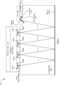
- FIG. 2 is a schematic illustrating thin film filters with a launching filter.
- a transceiver 200 with optical signals coupled via fibers 201 and a coupler 210.
- the coupler 210 comprises mirrors 203, glass 207, thin film filters (TFFs) 209, and a lens array 211.
- the coupler 210 may be configured to direct optical signals into photonics die 205 at near-normal incidence.
- the fibers 201 may comprise one or more optical fibers for coupling optical signals to and from the coupler 210 and photonics die 205 and may be within the fiber coupler 220, which may comprise lenses, filters, or polarization controlling components.
- the fiber coupler 220 may comprise a lens for focusing the optical signals from the fibers 201 onto the mirror 203, or focus signals from the mirror 203 to the fibers 203.
- the fiber coupler 220 may comprise polarization splitting components to spatially separate signals of different polarizations before reflecting off the mirror 203.
- the fibers may comprise single mode or multi-mode fiber. In an example scenario, one fiber is used to couple signals into the coupler 210 and subsequently to the photonics die 205, while a second fiber receives optical signals from the photonics die via the coupler 210.
- the glass 207 may comprise a machined and/or polished highly transparent structure on which optical components such as mirrors and filters may be formed.
- optical components such as mirrors and filters
- one or more layers of a highly reflective metal, such as gold, for example, may be deposited on highly polished surfaces of the glass 207, thereby forming mirror 203.
- filter structures may be formed by depositing stacks of dielectric layers on the glass 207, thereby forming the TFFs 209, for example. Accordingly, the glass 207 may guide optical signals from the fiber 201 end to the TFF 209 end, and vice versa.
- the lens array 211 may comprise a micro-machined silicon structure, for example, with lens structures formed therein that are operable to focus optical signals received from the TFFs 209 to specific spots on the photonics die 205, such as grating couplers. While convex lensing structures are shown, other shapes may be utilized depending on desired focal length, the dielectric constant of the lens material used, and space requirements, for example.
- the TFFs 209 may comprise stacks of alternating dielectric constant materials resulting in structures that are reflective at most wavelengths but allow light of specific wavelengths to pass through. Each of the TFFs 209 may be tuned to different wavelengths, which may be useful for CWDM applications. While four TFFs 209 are shown in FIG. 2 , any number of TFFs may be used depending on the number of desired different wavelengths.
- the mirrors 203 may comprise a highly reflective material, such as a metal, formed on the glass 207, for directing the optical signals to the TFFs 209 from the fibers 201.
- the fibers 201 may comprise collimators at their outputs for providing collimated beams to the coupler 210.
- optical signals may be coupled into the coupler 210 via the fibers 201 and reflected by the mirrors 203 and TFFs 209, resulting in a multi-reflection configuration.
- the TFFs 209 are each configured to reflect all signals except for those in a specific wavelength range.
- specific wavelength optical signals may be coupled to specific locations on the photonics die 205, preferably to grating couplers tuned to the specific wavelength.
- the mirrors 203 enable an essentially vertical impingement on the TFFs 209, so that further reflecting structures are not needed after the TFFs 209 for desired near-normal incidence on the photonics die 205, thereby maximizing the coupling efficiency of optical signals in to the photonics die 205.
- FIG. 3 is a schematic illustrating thin film filters integrated with collimating lenses.
- a transceiver 300 with optical signals coupled fiber coupler 310 and die coupler 320 The fiber coupler 310 comprises a lens 323, a V-groove 325, and a reflector 327.
- the fiber coupler 310 comprises two-fiber V-grooves for aligning two fibers 301 (with only one shown in the cross-section of FIG. 3 ).
- the fiber coupler 310 may also comprise polarization controlling components.
- the fiber coupler 310 may comprise a lens/filter 323 for focusing the optical signals from the fibers 301 onto the reflector 327, or focus signals from the reflector 327 to the fibers 301.
- the lens/filter 323 in the fiber coupler 310 may comprise polarization splitting components to spatially separate signals of different polarizations before reflecting off the reflector 327.
- the lens 323 may comprise a graded index (GRIN) lens, for example, for focusing optical signals from the fiber 301 onto the reflector 327 so that reflected signals impinge on the desired TFF 309A-309D, and also for focusing signals received from the photonics die 305 via the die coupler 320 into the fibers 301.
- the reflector 327 may comprise highly reflective material, such as a metal, to direct optical signals from the fiber 301 onto the first of the TFFs 309A-309D, resulting in a multi-reflection configuration.
- the die coupler 320 comprises glass 307 with mirror 303, thin film filters (TFFs) 309A-309D, and a lens array 311 formed thereon.
- the mirror 303 may be formed by depositing a highly reflective metal on the top surface of the glass 307 and may extend the length of the grating couplers 313A-313D in the photonics die 305 to allow for multiple reflections.
- the TFFs 309A-309D are each configured to reflect all optical signals except for those in a specific wavelength range. In this manner, specific wavelength optical signals may be coupled to corresponding grating couplers 313 on photonics die 305, tuned to a specific wavelength for that grating coupler.
- the mirror 303 and TFFs 309A-309D enable an essentially vertical impingement on the TFFs 309A-309D, so that further reflecting structures are not needed after the TFFs 309A-309D for desired near-normal incidence on the grating couplers 313A-313D on the photonics die 305.
- the lenses 311A-311D may comprise a micro-machined silicon structure, for example, that is operable to focus optical signals received from the TFFs 309A-309D to specific grating couplers 313A-313D, and also to focus optical signals from the photonics die 305 onto the TFFs 309A-309D.
- the TFFs 309A-309D and lenses 311A-311D may be formed and/or machined on the same structure. While convex lensing structures are shown, other shapes may be utilized depending on desired focal length, the dielectric constant of the lens material used, and space requirements, for example.
- the TFFs 309A-309D may comprise stacks of alternating dielectric constant materials resulting in structures that are reflective at most wavelengths but allow light of specific wavelengths to pass through. Each of the TFFs 309A-309D may be tuned to different wavelengths, which may be useful for CWDM applications. While four TFFs 309A-309D are shown in FIG. 3 , any number of TFFs may be used depending on the number of desired different wavelengths.
- the TFFs 309A-309D and lens array 311 subassembly may first be precision attached to the photonics die 305, followed by the fiber coupler 310 being actively aligned to the TFF 309A-309D and lenses 311A-311D subassembly.
- a CWDM4 optical signal may be coupled into the fiber coupler 310 via the fibers 301 and directed by the reflector 327 down to the first TFF 309A, where the optical signal with the wavelength that corresponds to TFF 309A will pass through to the lens 311A, while all other optical signals reflect up to the mirror 303.
- the reflected signals are again reflected down by the mirror 303, but to the second TFF 309B where a second wavelength optical signal passes through while the remaining signals are reflected to the mirror 303. This continues until the last remaining optical signal passes through the last TFF 309D and lens 311D to the last grating coupler 313D.
- a CWDM signal may be demultiplexed and processed individually by the photonic and electronic circuitry in the photonics die, as described previously with respect to FIG. 1 , for example.
- specific wavelength optical signals may be coupled to specific locations on the photonics die 305, to grating couplers tuned to the specific wavelength.
- the mirror 303 enables an essentially vertical impingement on the TFFs 309A-309D, so that further reflecting structures are not needed after the TFF 309D for desired near-normal incidence on the photonics die 305, thereby maximizing the coupling efficiency of optical signals in to the photonics die 305.
- FIG. 4 illustrates an integrated MUX/DEMUX with lenses integrated on silicon, in accordance with an example embodiment of the disclosure.
- a MUX/DEMUX 400 formed in a silicon substrate 405 with lenses/TFFs 407A-407D formed on one surface and a back-side mirror 403A formed on the opposite side.
- the lenses/TFFs 407A-407D may comprise lenses incorporated with TFFs, in that stacks of dielectric layers for TFFS may be deposited on lenses formed in the silicon substrate 405, for example.
- the lenses may be deposited on the Si substrate 405 and then dielectric stacks may then be formed on the lenses.
- the dielectric stacks may be configured such that only optical signals of a desired wavelength pass through to be focused by each lens.
- the fiber 401 may comprise a single mode or multi-mode fiber that is placed in a V-groove 415 formed in the Si substrate 405 for proper alignment.
- the lid 411 may comprise physical support and hermetic sealing, for example, for the optical end of fiber 401.
- the V-groove 415 may be formed in the silicon with an angled surface for receiving optical signals from the fiber 401, where the angled surface may comprise an anti-reflection (AR) coating 413 to reduce or eliminate unwanted reflections back into the fiber 401.
- AR anti-reflection
- the V-groove 415 and mirror angled surface may be formed in the same etch step, using potassium hydroxide (KOH), for example, which would give a degree of self-alignment.
- KOH potassium hydroxide
- etch which follows crystal planes, may enable exceptionally tight angle control.
- the various planes of the mirrors and V-groove are defined by crystallographic axes of the silicon.
- An opposite surface to the AR coating 413 may be coated with a highly reflective metal to form mirror 403B.
- the arrangement of the AR coating, mirrors 403A and 403B, and lenses/TFFs 407A-407D enable a multi-reflection configuration, where at each lens/TFF 407A-407D most wavelengths are reflected while only a desired wavelength is transmitted through the lens/TFF 407A-407D to a coupler on a photonics die.
- Utilizing a silicon substrate for the MUX/DEMUX 400 may enable tight thickness and coplanarity control for the multi-reflection configuration.
- the Si substrate 405 may be ⁇ 1.5 mm thick and the angle of reflection at the backside mirror 403A may be ⁇ 12.8 degrees, in that an incoming optical signal is at 6.4 degrees from normal incidence.
- a CWDM4 optical signal may be coupled into the MUX/DEMUX 400 via the fiber 401 and angled slightly downward by the change of index of refraction of the Si substrate 405, before being reflected downward by the mirror 403B to the backside mirror 403A.
- the angle of the mirror 403B may be configured such that the reflection of the optical beam is such that it is centered on the lens/TFF 407A when reflected back upward by the backside mirror 403A.
- the angle of the mirror 403B may be defined by crystalline planes of the silicon, formed by anisotropic etching, for example, thereby enabling very tight distribution of this angle.
- a first wavelength optical signal, ⁇ 1 in this example passes through while the remaining wavelength optical signals are reflected back downward to the backside mirror 403A.
- the optical signal at wavelength ⁇ 1 is coupled to a photonics die coupled to the MUX/DEMUX 400.
- the optical signal After being reflected by the lens/TFF 407A, the optical signal thus comprises signals of wavelengths ⁇ 2 - ⁇ 4 , as indicated in FIG. 4 at the second reflection at the backside mirror 403A.
- This signal then reaches the lens/TFF 407B where the ⁇ 2 wavelength optical signal passes through while the ⁇ 3 and ⁇ 4 wavelength signals are reflected back to the backside mirror 403A.
- This reflection and transmission continues until each optical signal is communicated through one of the lenses/TFFs 407A-407D, demonstrating a CWDM4 demultiplexer.
- a four wavelength DEMUX is shown in FIG. 4 , any number of wavelengths may be demultiplexed based on the number of lenses/TFFs incorporated in the structure.
- the MUX/DEMUX 400 may multiplex signals by essentially operating in the reverse direction to that described above.
- optical signals of four different wavelengths may be received from a photonic chip, pass through the corresponding lens/TFF 407A-407D and be reflected by the backside mirror 403A.
- each signal will thus be reflected by the other lenses/TFFs 407A-407D to the backside mirror 403A consecutively until reaching the mirror 403B and AR coating 413, before being coupled into the fiber 401, thereby generating a CWDM4 signal.
- FIG. 5 illustrates an integrated MUX/DEMUX with thin film filters integrated on silicon and coupled to a lens array and photonics die, in accordance with an example embodiment of the disclosure.
- a MUX/DEMUX 500 formed in a silicon substrate 505 with TFFs 509A-509D formed on one surface and a back-side mirror 503A formed on the opposite side.
- the TFFs 509A-509D may comprise dielectric stacks that may be configured such that only optical signals of a desired wavelength pass through while reflecting other optical wavelengths.
- the lenses 507A-507D may comprise lenses formed in or on a silicon substrate and may be operable to focus received signals onto corresponding grating couplers in the photonics die 510. In addition, the lenses 507A-507D may be operable to focus optical signals received from grating couplers in the photonics die 510 to the TFFs 509A-509D.
- the fiber 501 may comprise a single mode or multi-mode fiber that is placed in a V-groove 515 formed in the Si substrate 505 for proper alignment.
- the lid 511 may comprise physical support and hermetic sealing, for example, for the optical end of fiber 501.
- the V-groove 515 may be formed in the silicon with an angled surface for receiving optical signals from the fiber 501, where the angled surface may comprise an anti-reflection (AR) coating 513 to reduce or eliminate unwanted reflections back into the fiber 501.
- AR anti-reflection
- the V-groove 515 and mirror angled surface may be formed in the same etch step, using potassium hydroxide (KOH), for example, which would give a degree of self-alignment.
- KOH potassium hydroxide
- etch which follows crystal planes, may enable exceptionally tight angle control.
- the various planes of the mirrors and V-groove are defined by crystallographic axes of the silicon.
- An opposite surface to the AR coating 513 may be coated with a highly reflective metal to form mirror 503B.
- the arrangement of the AR coating, mirrors 503A and 53B, and TFFs 509A-509D enable a multi-reflection configuration, where at each TFF 509A-509D most wavelengths are reflected while only a desired wavelength is transmitted through the TFF 509A-509D to a corresponding lens 507A-507D before being coupled to the photonics die 510.
- Utilizing silicon substrates for the MUX/DEMUX 500 may enable tight thickness and coplanarity control for the multi-reflection configuration.
- the Si substrate 505 may be ⁇ 1.5 mm thick and the angle of reflection at the backside mirror 403A may be ⁇ 12.8 degrees, in that an incoming optical signal is at 6.4 degrees from normal incidence.
- a CWDM4 optical signal may be coupled into the MUX/DEMUX 500 via the fiber 501 and angled slightly downward by the change of index of refraction of the Si substrate 505, before being reflected downward by the mirror 503B to the backside mirror 503A.
- the angle of the mirror 503B may be configured such that the reflection of the optical beam is such that it is centered on the TFF 509A when reflected back upward by the backside mirror 503A.
- the angle of the mirror 503B may be defined by crystalline planes of the silicon, formed by anisotropic etching, for example, thereby enabling very tight distribution of this angle.
- a first wavelength optical signal, ⁇ 1 in this example passes through while the remaining wavelength optical signals are reflected back downward to the backside mirror 503A.
- the optical signal at wavelength ⁇ 1 may be focused by the lens 507A to be coupled to the photonics die 510.
- the optical signal After being reflected by the TFF 509A, the optical signal thus comprises signals of wavelengths ⁇ 2 - ⁇ 4 , as indicated in FIG. 5 at the second reflection at the backside mirror 503A.
- This signal then reaches the TFF 509B where the ⁇ 2 wavelength optical signal passes through while the ⁇ 3 and ⁇ 4 wavelength signals are reflected back to the backside mirror 503A.
- This reflection and transmission continues until each optical signal is communicated through one of the TFFs 509A-509D, demonstrating a CWDM4 demultiplexer.
- a four wavelength DEMUX is shown in FIG. 5 , any number of wavelengths may be demultiplexed based on the number of lenses and TFFs incorporated in the structure.
- the MUX/DEMUX 500 may multiplex signals by essentially operating in the reverse direction to that described above.
- optical signals of four different wavelengths may be received from the photonics die 510, pass through the corresponding lens 507A-507D and TFF 509A-509D and be reflected by the backside mirror 503A.
- each signal will thus be reflected by the other TFFs 509A-509C to the backside mirror 503A consecutively until reaching the mirror 503B and AR coating 513, before being coupled into the fiber 501, thereby generating a CWDM4 signal.
Landscapes
- Physics & Mathematics (AREA)
- General Physics & Mathematics (AREA)
- Optics & Photonics (AREA)
- Optical Couplings Of Light Guides (AREA)
- Optical Communication System (AREA)
Claims (14)
- Ein Verfahren zur Kommunikation, wobei das Verfahren Folgendes aufweist:in einem optischen Demultiplexer, der an einen Photonik-Chip gekoppelt ist, wobei der optische Demultiplexer eine Vielzahl von Dünnschichtfiltern (407A-D) aufweist, die auf einer ersten Oberfläche eines Substrats (405) ausgebildet sind,eine Eingangsfasern (401), die in einer V-Nut (415) der ersten Oberfläche des Substrats (405) angeordnet ist,einen ersten Spiegel (403B) auf einer geneigten Fläche, die in der ersten Oberfläche des Substrats (405) ausgebildet ist,und einen zweiten Spiegel (403A), der auf einer zweiten, der ersten Oberfläche des Substrats (405) gegenüberliegenden Oberfläche ausgebildet ist:Empfangen eines Eingang-Optiksignals, das eine Vielzahl von optischen Signalen unterschiedlicher Wellenlänge aufweist, über die Eingangsfasern;Reflektieren des Eingang-Optiksignals von dem ersten Spiegel (403B) zu dem zweiten Spiegel (403A);Reflektieren des Eingang-Optiksignals von dem zweiten Spiegel (403A) zu einem ersten der Vielzahl von Dünnschichtfiltern (407A-D);Übertragen eines optischen Signals bei einer ersten Wellenlänge der Vielzahl von optischen Signalen unterschiedlicher Wellenlänge an den Photonik-Chip, während andere der Vielzahl von optischen Signalen unterschiedlicher Wellenlänge zu dem zweiten Spiegel (403A) reflektiert werden;Reflektieren der anderen der Vielzahl von optischen Signalen unterschiedlicher Wellenlänge von dem zweiten Spiegel (403A) zu einem zweiten der Vielzahl von Dünnschichtfiltern (407A-D); undÜbertragen eines optischen Signals bei einer zweiten Wellenlänge der Vielzahl von optischen Signalen unterschiedlicher Wellenlänge an den Photonik-Chip, wobei das Substrat (405) Silizium aufweist.
- Das Verfahren nach Anspruch 1 aufweisend, das Reflektieren der anderen der Vielzahl von optischen Signalen unterschiedlicher Wellenlänge über die Dünnschichtfilter (407A-D) und den zweiten Spiegel (403A), bis ein einziges optisches Signal einer Wellenlänge verbleibt und über einen letzten der Vielzahl von Dünnschichtfilter (407A-D) an den Photonik-Chip übertragen wird.
- Das Verfahren nach Anspruch 1, wobei eine Linse an die Eingangsfasern gekoppelt ist.
- Das Verfahren nach Anspruch 1, wobei der erste Spiegel (403B) und die V-Nut (415) durch kristallographische Achsen des Siliziumsubstrats (405) definiert sind.
- Das Verfahren nach Anspruch 1 aufweisend, das Übertragen der optischen Signale bei der ersten und zweiten Wellenlänge an den Photonik-Chip durch Fokussierlinsen,
wobei das Verfahren optional das Fokussieren der optischen Signale bei der ersten und zweiten Wellenlänge auf Gitterkoppler im Photonik-Chip unter Verwendung der Fokussierlinsen aufweist. - Ein System zur Kommunikation, wobei das System Folgendes aufweist:einen optischen Demultiplexer, der an einen Photonik-Chip gekoppelt ist, wobei der optische Demultiplexer eine Vielzahl von Dünnschichtfiltern (407A-D) aufweist, die auf einer ersten Oberfläche eines Substrats (405) ausgebildet sind,eine Eingangsfasern (401), die in einer V-Nut (415) der ersten Oberfläche des Substrats (405) angeordnet ist,einen ersten Spiegel (403B) auf einer geneigten Fläche, die in der ersten Oberfläche des Substrats (405) ausgebildet ist,und einen zweiten Spiegel (403A), der auf einer zweiten, der ersten Oberfläche des Substrats (405) gegenüberliegenden Oberfläche ausgebildet ist, wobei der optische Demultiplexer dazu betriebsfähig ist:ein über die Eingangsfasern empfangenes Eingang-Optiksignal, das eine Vielzahl von optischen Signalen unterschiedlicher Wellenlänge aufweist, aufzunehmen;das Eingang-Optiksignal von dem ersten Spiegel (403B) zu dem zweiten Spiegel (403A) zu reflektieren;das Eingang-Optiksignal von dem zweiten Spiegel (403A) zu einem ersten der Vielzahl von Dünnschichtfilter (407A-D) zu reflektieren;ein optisches Signal bei einer ersten Wellenlänge der Vielzahl von optischen Signalen unterschiedlicher Wellenlänge an den Photonik-Chip zu übertragen, während andere der Vielzahl von optischen Signalen unterschiedlicher Wellenlänge zu dem zweiten Spiegel (403A) reflektiert werden;die anderen der Vielzahl von optischen Signalen unterschiedlicher Wellenlänge von dem zweiten Spiegel (403A) zu einem zweiten der Vielzahl von Dünnschichtfilter (407A-D) zu reflektieren; undein optisches Signal bei einer zweiten Wellenlänge der Vielzahl von optischen Signalen unterschiedlicher Wellenlänge an den Photonik-Chip zu übertragen, wobei das Substrat (405) Silizium aufweist.
- Das System nach Anspruch 6, wobei der optische Demultiplexer dazu betriebsfähig ist, die anderen der Vielzahl von optischen Signalen unterschiedlicher Wellenlänge über die Dünnschichtfilter (407A-D) und den zweiten Spiegel (403A) zu reflektieren, bis ein einziges optisches Signal einer Wellenlänge verbleibt und über einen letzten der Vielzahl von Dünnschichtfilter (407A-D) an den Photonik-Chip übertragen wird.
- Das System nach Anspruch 6, wobei eine Linse an die Eingangsfasern gekoppelt ist.
- Das System nach Anspruch 6, wobei der erste Spiegel (403B) und die V-Nut (415) durch kristallographische Achsen des Siliziumsubstrats (405) definiert sind.
- Das System nach Anspruch 6, wobei der optische Demultiplexer dazu betriebsfähig ist, die optischen Signale bei der ersten und zweiten Wellenlänge durch Fokussierlinsen an den Photonik-Chip zu übertragen,
optional wobei der optische Demultiplexer dazu betriebsfähig ist, die optischen Signale bei der ersten und zweiten Wellenlänge unter Verwendung der Fokussierlinsen auf Gitterkoppler im Photonik-Chip zu fokussieren. - Ein System zur Kommunikation, wobei das System Folgendes aufweist:
einen optischen Multiplexer, der an einen Photonik-Chip gekoppelt ist, wobei der optische Multiplexer Folgendes aufweist:eine Vielzahl von Dünnschichtfiltern (407A-D), die auf einer ersten Oberfläche eines Substrats (405) ausgebildet sind,eine Ausgangsoptikfaser (401), die in einer V-Nut (415) der ersten Oberfläche des Substrats (405) angeordnet ist,einen ersten Spiegel (403B) auf einer geneigten Fläche, die in der ersten Oberfläche des Substrats (405) ausgebildet ist,und einen zweiten Spiegel (403A), der auf einer zweiten, der ersten Oberfläche des Substrats (405) gegenüberliegenden Oberfläche ausgebildet ist,wobei der optische Multiplexer dazu betriebsfähig ist:eine Vielzahl von Eingangs-Optiksignalen, die jeweils eine unterschiedliche Wellenlänge aufweisen, von dem Photonik-Chip zu empfangen;jedes der Vielzahl von Eingangs-Optiksignalen durch einen entsprechenden Dünnschichtfilter der Vielzahl von Dünnschichtfilter (407A-D) in das Substrat (405) zu übertragen;die übertragene Vielzahl von Eingangs-Optiksignalen nacheinander von dem zweiten Spiegel (403A) und einer Teilmenge der Dünnschichtfilter (407A-D) zu reflektieren, bis jedes Eingangs-Optiksignal zu dem ersten Spiegel (403B) reflektiert ist; undein multiplexes Optiksignal, das die Vielzahl von Eingangs-Optiksignalen aufweist, von dem ersten Spiegel (403B) in die Ausgangsoptikfaser (401) zu übertragen, wobei das Substrat (405) Silizium aufweist. - Das System nach Anspruch 11, wobei eine Linse an die Ausgangsoptikfaser gekoppelt ist.
- Das System nach Anspruch 11, wobei der erste Spiegel (403B) und die V-Nut (415) durch kristallographische Achsen des Siliziumsubstrats (405) definiert sind.
- Das System nach Anspruch 11, wobei der optische Multiplexer dazu betriebsfähig ist, jedes der empfangenen Vielzahl von Eingangs-Optiksignalen durch Fokussierlinsen zu übertragen,
optional wobei die Fokussierlinsen die Vielzahl von Eingangs-Optiksignalen auf einen entsprechenden Dünnschichtfilter (407A-D) fokussieren.
Applications Claiming Priority (2)
| Application Number | Priority Date | Filing Date | Title |
|---|---|---|---|
| US201762571567P | 2017-10-12 | 2017-10-12 | |
| PCT/US2018/055681 WO2019075377A1 (en) | 2017-10-12 | 2018-10-12 | METHOD AND SYSTEM FOR QUASIALLY NORMAL INCIDENCE MULTIPLEXER / DEMULTIPLEXER DESIGN |
Publications (3)
| Publication Number | Publication Date |
|---|---|
| EP3695256A1 EP3695256A1 (de) | 2020-08-19 |
| EP3695256A4 EP3695256A4 (de) | 2021-07-07 |
| EP3695256B1 true EP3695256B1 (de) | 2025-02-12 |
Family
ID=66095753
Family Applications (1)
| Application Number | Title | Priority Date | Filing Date |
|---|---|---|---|
| EP18867026.9A Active EP3695256B1 (de) | 2017-10-12 | 2018-10-12 | Verfahren und system für mux/demux-entwürfe mit fast normalem einfall |
Country Status (4)
| Country | Link |
|---|---|
| US (1) | US11022756B2 (de) |
| EP (1) | EP3695256B1 (de) |
| CN (1) | CN111263906A (de) |
| WO (1) | WO2019075377A1 (de) |
Families Citing this family (4)
| Publication number | Priority date | Publication date | Assignee | Title |
|---|---|---|---|---|
| US10469195B2 (en) * | 2017-10-12 | 2019-11-05 | Luxtera, Inc. | Method and system for eliminating polarization dependence for 45 degree incidence MUX/DEMUX designs |
| WO2020197532A1 (en) * | 2019-03-22 | 2020-10-01 | Source Photonics, Inc. | System and method for transferring optical signals in photonic devices and method of making the system |
| US12339498B2 (en) | 2020-02-26 | 2025-06-24 | Rheinisch-Westfälische Technische Hochschule (Rwth) Aachen | Optical coupler comprising a molded optical interposer together with a PIC and 2 polarization selective elements enabling isolation and/or polarization management |
| US20240369772A1 (en) * | 2023-05-01 | 2024-11-07 | Cisco Technology, Inc. | Wavelength multiplexing or demultiplexing using a lens array with an angled facet |
Family Cites Families (34)
| Publication number | Priority date | Publication date | Assignee | Title |
|---|---|---|---|---|
| US5687263A (en) * | 1995-10-02 | 1997-11-11 | The United States Of America As Represented By The Secretary Of The Navy | Optical RF bandpass filter and method for manufacturing same |
| US6198864B1 (en) * | 1998-11-24 | 2001-03-06 | Agilent Technologies, Inc. | Optical wavelength demultiplexer |
| US6201908B1 (en) * | 1999-07-02 | 2001-03-13 | Blaze Network Products, Inc. | Optical wavelength division multiplexer/demultiplexer having preformed passively aligned optics |
| DE10043324A1 (de) * | 2000-08-23 | 2002-03-14 | Infineon Technologies Ag | Opto-elektronische Baugruppe zum Multiplexen und/oder Demultiplexen optischer Signale |
| US6751379B2 (en) * | 2000-11-01 | 2004-06-15 | Intel Corporation | System and method for collimating and redirecting beams in a fiber optic system |
| US6804429B2 (en) * | 2001-02-09 | 2004-10-12 | The Board Of Trustees Of The Leland Stanford Junior University | Reconfigurable wavelength multiplexers and filters employing micromirror array in a gires-tournois interferometer |
| US6870976B2 (en) * | 2001-03-13 | 2005-03-22 | Opnext, Inc. | Filter based multiplexer/demultiplexer component |
| WO2003012505A1 (de) * | 2001-07-02 | 2003-02-13 | Infineon Technologies Ag | Vorrichtung und verfahren zum multiplexen und/oder demultiplexen optischer signale einer mehrzahl von wellenlängen |
| US6748133B2 (en) * | 2001-11-26 | 2004-06-08 | Alliance Fiber Optic Products, Inc. | Compact multiplexing/demultiplexing modules |
| US6769816B2 (en) * | 2002-08-28 | 2004-08-03 | Intel Corporation | Multi-wavelength transceiver device with integration on transistor-outline cans |
| US20050069013A1 (en) * | 2003-09-29 | 2005-03-31 | Photodigm, Inc. | Method and apparatus for wavelength division multiplexing |
| US20060251422A1 (en) * | 2005-05-06 | 2006-11-09 | Jian Liu | Power and energy scaling of fiber lasers by using compact divisional wavelength multiplexing (WDM) devices |
| WO2006134675A1 (ja) | 2005-06-14 | 2006-12-21 | Nippon Telegraph And Telephone Corporation | 光合分波器およびその組み立て装置 |
| US7366371B1 (en) * | 2006-11-21 | 2008-04-29 | Finisar Corporation | Compact optical multiplexer and demultiplexer |
| JP2010186090A (ja) * | 2009-02-13 | 2010-08-26 | Hitachi Ltd | 光送受信モジュール |
| EP2312352B1 (de) * | 2009-09-07 | 2018-04-18 | Electronics and Telecommunications Research Institute | Optische Übertragung mit mehreren Wellenlängen und Empfangsmodule |
| KR101144665B1 (ko) * | 2010-09-20 | 2012-05-24 | 옵티시스 주식회사 | 파장 분할 다중화 및 역다중화 장치 |
| KR101434397B1 (ko) * | 2010-11-22 | 2014-09-05 | 한국전자통신연구원 | 다채널 광 모듈 |
| US8913858B2 (en) * | 2012-03-30 | 2014-12-16 | Corning Cable Systems Llc | Total-internal-reflection fiber optic interface modules and assemblies |
| US9435963B2 (en) * | 2012-03-30 | 2016-09-06 | Corning Cable Systems Llc | Misalignment-tolerant total-internal-reflection fiber optic interface modules and assemblies with high coupling efficiency |
| US9323013B2 (en) * | 2013-04-19 | 2016-04-26 | Avago Technologies General Ip (Singapore) Pte. Ltd. | Bidirectional optical communications module having an optics system that reduces optical losses and increases tolerance to optical misalignment |
| WO2015026335A1 (en) * | 2013-08-21 | 2015-02-26 | Hewlett-Packard Development Company, L.P. | Device including mirrors and filters to operate as a multiplexer or de-multiplexer |
| EP3063574B1 (de) * | 2013-10-31 | 2022-03-02 | Hewlett Packard Enterprise Development LP | Gemultiplexte optoelektronische engines |
| WO2015112169A1 (en) * | 2014-01-25 | 2015-07-30 | Hewlett-Packard Development Company, L.P. | Bidirectional optical multiplexing employing a high contrast grating |
| CN203849457U (zh) * | 2014-05-28 | 2014-09-24 | 奥普镀膜技术(广州)有限公司 | 小间距型光学解复用器 |
| US10243661B2 (en) * | 2014-08-15 | 2019-03-26 | Hewlett Packard Enterprise Development Lp | Optical mode matching |
| WO2016122678A1 (en) * | 2015-01-31 | 2016-08-04 | Hewlett Packard Enterprise Development Lp | Optical multiplexer |
| WO2016164038A1 (en) * | 2015-04-10 | 2016-10-13 | Hewlett Packard Enterprise Development Lp | Optical zig-zags |
| US9804334B2 (en) * | 2015-10-08 | 2017-10-31 | Teramount Ltd. | Fiber to chip optical coupler |
| US9854336B2 (en) * | 2015-12-31 | 2017-12-26 | Infinera Corporation | Systems and methods for coupling a fiber to a polarization sensitive photonic integrated circuit |
| US20180017735A1 (en) * | 2016-07-13 | 2018-01-18 | Futurewei Technologies, Inc. | Wavelength Division Multiplexer/Demultiplexer with Flexibility of Optical Adjustment |
| JP2018017649A (ja) * | 2016-07-29 | 2018-02-01 | 北日本電線株式会社 | 光分波器 |
| US9798087B1 (en) * | 2016-11-01 | 2017-10-24 | Hewlett Packard Enterprise Development Lp | Optoelectronic devices and wavelength-division multiplexing optical connectors |
| US10409013B1 (en) * | 2018-10-05 | 2019-09-10 | Orangetek Corporation | Optical fiber module |
-
2018
- 2018-10-12 CN CN201880066392.8A patent/CN111263906A/zh active Pending
- 2018-10-12 EP EP18867026.9A patent/EP3695256B1/de active Active
- 2018-10-12 WO PCT/US2018/055681 patent/WO2019075377A1/en unknown
- 2018-10-12 US US16/159,174 patent/US11022756B2/en active Active
Also Published As
| Publication number | Publication date |
|---|---|
| EP3695256A4 (de) | 2021-07-07 |
| US20190113687A1 (en) | 2019-04-18 |
| US11022756B2 (en) | 2021-06-01 |
| CN111263906A (zh) | 2020-06-09 |
| EP3695256A1 (de) | 2020-08-19 |
| WO2019075377A1 (en) | 2019-04-18 |
Similar Documents
| Publication | Publication Date | Title |
|---|---|---|
| EP3864776B1 (de) | Verfahren und system für cwdm-mux/demux-designs für siliziumphotonik-interposer | |
| US10892845B2 (en) | Method and system for a free space CWDM MUX/DEMUX for integration with a grating coupler based silicon photonics platform | |
| US11018796B2 (en) | Method and system for eliminating polarization dependence for 45 degree incidence MUX/DEMUX designs | |
| US20190052362A1 (en) | Method And System For A Free Space CWDM MUX/DEMUX For Integration With A Grating Coupler Based Silicon Photonics Platform | |
| US10120126B2 (en) | Method and system for partial integration of wavelength division multiplexing and bi-directional solutions | |
| EP3695256B1 (de) | Verfahren und system für mux/demux-entwürfe mit fast normalem einfall | |
| US10439727B2 (en) | Method and system for selectable parallel optical fiber and wavelength division multiplexed operation | |
| US11201675B2 (en) | Method and system for a bi-directional multi-wavelength receiver for standard single-mode fiber based on grating couplers | |
| EP3665519A1 (de) | Freiraum-cwdm-mux/demux zur integration mit einer fotonischen siliziumplattform | |
| US20230081747A1 (en) | High density fiber interfaces for silicon photonics based integrated-optics products |
Legal Events
| Date | Code | Title | Description |
|---|---|---|---|
| STAA | Information on the status of an ep patent application or granted ep patent |
Free format text: STATUS: THE INTERNATIONAL PUBLICATION HAS BEEN MADE |
|
| PUAI | Public reference made under article 153(3) epc to a published international application that has entered the european phase |
Free format text: ORIGINAL CODE: 0009012 |
|
| STAA | Information on the status of an ep patent application or granted ep patent |
Free format text: STATUS: REQUEST FOR EXAMINATION WAS MADE |
|
| 17P | Request for examination filed |
Effective date: 20200504 |
|
| AK | Designated contracting states |
Kind code of ref document: A1 Designated state(s): AL AT BE BG CH CY CZ DE DK EE ES FI FR GB GR HR HU IE IS IT LI LT LU LV MC MK MT NL NO PL PT RO RS SE SI SK SM TR |
|
| AX | Request for extension of the european patent |
Extension state: BA ME |
|
| DAV | Request for validation of the european patent (deleted) | ||
| DAX | Request for extension of the european patent (deleted) | ||
| A4 | Supplementary search report drawn up and despatched |
Effective date: 20210609 |
|
| RIC1 | Information provided on ipc code assigned before grant |
Ipc: G02B 6/293 20060101AFI20210602BHEP Ipc: G02B 6/12 20060101ALI20210602BHEP Ipc: G02B 6/42 20060101ALI20210602BHEP Ipc: H04J 14/02 20060101ALI20210602BHEP Ipc: H04J 14/06 20060101ALI20210602BHEP Ipc: H04Q 11/00 20060101ALI20210602BHEP Ipc: G02B 6/30 20060101ALN20210602BHEP Ipc: G02B 6/32 20060101ALN20210602BHEP |
|
| RIN1 | Information on inventor provided before grant (corrected) |
Inventor name: MASINI, GIANLORENZO Inventor name: SAHNI, SUBAL Inventor name: WANG, SHAWN |
|
| STAA | Information on the status of an ep patent application or granted ep patent |
Free format text: STATUS: EXAMINATION IS IN PROGRESS |
|
| 17Q | First examination report despatched |
Effective date: 20220907 |
|
| P01 | Opt-out of the competence of the unified patent court (upc) registered |
Effective date: 20230525 |
|
| GRAP | Despatch of communication of intention to grant a patent |
Free format text: ORIGINAL CODE: EPIDOSNIGR1 |
|
| STAA | Information on the status of an ep patent application or granted ep patent |
Free format text: STATUS: GRANT OF PATENT IS INTENDED |
|
| RIC1 | Information provided on ipc code assigned before grant |
Ipc: G02B 6/32 20060101ALN20240808BHEP Ipc: G02B 6/30 20060101ALN20240808BHEP Ipc: H04Q 11/00 20060101ALI20240808BHEP Ipc: H04J 14/06 20060101ALI20240808BHEP Ipc: H04J 14/02 20060101ALI20240808BHEP Ipc: G02B 6/42 20060101ALI20240808BHEP Ipc: G02B 6/12 20060101ALI20240808BHEP Ipc: G02B 6/293 20060101AFI20240808BHEP |
|
| INTG | Intention to grant announced |
Effective date: 20240910 |
|
| GRAS | Grant fee paid |
Free format text: ORIGINAL CODE: EPIDOSNIGR3 |
|
| GRAA | (expected) grant |
Free format text: ORIGINAL CODE: 0009210 |
|
| STAA | Information on the status of an ep patent application or granted ep patent |
Free format text: STATUS: THE PATENT HAS BEEN GRANTED |
|
| AK | Designated contracting states |
Kind code of ref document: B1 Designated state(s): AL AT BE BG CH CY CZ DE DK EE ES FI FR GB GR HR HU IE IS IT LI LT LU LV MC MK MT NL NO PL PT RO RS SE SI SK SM TR |
|
| REG | Reference to a national code |
Ref country code: GB Ref legal event code: FG4D |
|
| REG | Reference to a national code |
Ref country code: CH Ref legal event code: EP |
|
| REG | Reference to a national code |
Ref country code: DE Ref legal event code: R096 Ref document number: 602018079166 Country of ref document: DE |
|
| REG | Reference to a national code |
Ref country code: IE Ref legal event code: FG4D |
|
| REG | Reference to a national code |
Ref country code: NL Ref legal event code: MP Effective date: 20250212 |
|
| PG25 | Lapsed in a contracting state [announced via postgrant information from national office to epo] |
Ref country code: RS Free format text: LAPSE BECAUSE OF FAILURE TO SUBMIT A TRANSLATION OF THE DESCRIPTION OR TO PAY THE FEE WITHIN THE PRESCRIBED TIME-LIMIT Effective date: 20250512 |
|
| PG25 | Lapsed in a contracting state [announced via postgrant information from national office to epo] |
Ref country code: FI Free format text: LAPSE BECAUSE OF FAILURE TO SUBMIT A TRANSLATION OF THE DESCRIPTION OR TO PAY THE FEE WITHIN THE PRESCRIBED TIME-LIMIT Effective date: 20250212 |
|
| PG25 | Lapsed in a contracting state [announced via postgrant information from national office to epo] |
Ref country code: PL Free format text: LAPSE BECAUSE OF FAILURE TO SUBMIT A TRANSLATION OF THE DESCRIPTION OR TO PAY THE FEE WITHIN THE PRESCRIBED TIME-LIMIT Effective date: 20250212 |
|
| PG25 | Lapsed in a contracting state [announced via postgrant information from national office to epo] |
Ref country code: ES Free format text: LAPSE BECAUSE OF FAILURE TO SUBMIT A TRANSLATION OF THE DESCRIPTION OR TO PAY THE FEE WITHIN THE PRESCRIBED TIME-LIMIT Effective date: 20250212 |