EP3694297A2 - Method for repairing coated printed circuit boards - Google Patents
Method for repairing coated printed circuit boards Download PDFInfo
- Publication number
- EP3694297A2 EP3694297A2 EP19210326.5A EP19210326A EP3694297A2 EP 3694297 A2 EP3694297 A2 EP 3694297A2 EP 19210326 A EP19210326 A EP 19210326A EP 3694297 A2 EP3694297 A2 EP 3694297A2
- Authority
- EP
- European Patent Office
- Prior art keywords
- pcb
- recoating
- printed circuit
- repairing
- circuit board
- Prior art date
- Legal status (The legal status is an assumption and is not a legal conclusion. Google has not performed a legal analysis and makes no representation as to the accuracy of the status listed.)
- Pending
Links
Images


Classifications
-
- H—ELECTRICITY
- H05—ELECTRIC TECHNIQUES NOT OTHERWISE PROVIDED FOR
- H05K—PRINTED CIRCUITS; CASINGS OR CONSTRUCTIONAL DETAILS OF ELECTRIC APPARATUS; MANUFACTURE OF ASSEMBLAGES OF ELECTRICAL COMPONENTS
- H05K3/00—Apparatus or processes for manufacturing printed circuits
- H05K3/22—Secondary treatment of printed circuits
- H05K3/28—Applying non-metallic protective coatings
- H05K3/288—Removal of non-metallic coatings, e.g. for repairing
-
- H—ELECTRICITY
- H05—ELECTRIC TECHNIQUES NOT OTHERWISE PROVIDED FOR
- H05K—PRINTED CIRCUITS; CASINGS OR CONSTRUCTIONAL DETAILS OF ELECTRIC APPARATUS; MANUFACTURE OF ASSEMBLAGES OF ELECTRICAL COMPONENTS
- H05K3/00—Apparatus or processes for manufacturing printed circuits
- H05K3/22—Secondary treatment of printed circuits
- H05K3/28—Applying non-metallic protective coatings
- H05K3/284—Applying non-metallic protective coatings for encapsulating mounted components
-
- C—CHEMISTRY; METALLURGY
- C23—COATING METALLIC MATERIAL; COATING MATERIAL WITH METALLIC MATERIAL; CHEMICAL SURFACE TREATMENT; DIFFUSION TREATMENT OF METALLIC MATERIAL; COATING BY VACUUM EVAPORATION, BY SPUTTERING, BY ION IMPLANTATION OR BY CHEMICAL VAPOUR DEPOSITION, IN GENERAL; INHIBITING CORROSION OF METALLIC MATERIAL OR INCRUSTATION IN GENERAL
- C23C—COATING METALLIC MATERIAL; COATING MATERIAL WITH METALLIC MATERIAL; SURFACE TREATMENT OF METALLIC MATERIAL BY DIFFUSION INTO THE SURFACE, BY CHEMICAL CONVERSION OR SUBSTITUTION; COATING BY VACUUM EVAPORATION, BY SPUTTERING, BY ION IMPLANTATION OR BY CHEMICAL VAPOUR DEPOSITION, IN GENERAL
- C23C16/00—Chemical coating by decomposition of gaseous compounds, without leaving reaction products of surface material in the coating, i.e. chemical vapour deposition [CVD] processes
- C23C16/02—Pretreatment of the material to be coated
- C23C16/0227—Pretreatment of the material to be coated by cleaning or etching
-
- C—CHEMISTRY; METALLURGY
- C23—COATING METALLIC MATERIAL; COATING MATERIAL WITH METALLIC MATERIAL; CHEMICAL SURFACE TREATMENT; DIFFUSION TREATMENT OF METALLIC MATERIAL; COATING BY VACUUM EVAPORATION, BY SPUTTERING, BY ION IMPLANTATION OR BY CHEMICAL VAPOUR DEPOSITION, IN GENERAL; INHIBITING CORROSION OF METALLIC MATERIAL OR INCRUSTATION IN GENERAL
- C23C—COATING METALLIC MATERIAL; COATING MATERIAL WITH METALLIC MATERIAL; SURFACE TREATMENT OF METALLIC MATERIAL BY DIFFUSION INTO THE SURFACE, BY CHEMICAL CONVERSION OR SUBSTITUTION; COATING BY VACUUM EVAPORATION, BY SPUTTERING, BY ION IMPLANTATION OR BY CHEMICAL VAPOUR DEPOSITION, IN GENERAL
- C23C16/00—Chemical coating by decomposition of gaseous compounds, without leaving reaction products of surface material in the coating, i.e. chemical vapour deposition [CVD] processes
- C23C16/04—Coating on selected surface areas, e.g. using masks
- C23C16/042—Coating on selected surface areas, e.g. using masks using masks
-
- C—CHEMISTRY; METALLURGY
- C23—COATING METALLIC MATERIAL; COATING MATERIAL WITH METALLIC MATERIAL; CHEMICAL SURFACE TREATMENT; DIFFUSION TREATMENT OF METALLIC MATERIAL; COATING BY VACUUM EVAPORATION, BY SPUTTERING, BY ION IMPLANTATION OR BY CHEMICAL VAPOUR DEPOSITION, IN GENERAL; INHIBITING CORROSION OF METALLIC MATERIAL OR INCRUSTATION IN GENERAL
- C23C—COATING METALLIC MATERIAL; COATING MATERIAL WITH METALLIC MATERIAL; SURFACE TREATMENT OF METALLIC MATERIAL BY DIFFUSION INTO THE SURFACE, BY CHEMICAL CONVERSION OR SUBSTITUTION; COATING BY VACUUM EVAPORATION, BY SPUTTERING, BY ION IMPLANTATION OR BY CHEMICAL VAPOUR DEPOSITION, IN GENERAL
- C23C16/00—Chemical coating by decomposition of gaseous compounds, without leaving reaction products of surface material in the coating, i.e. chemical vapour deposition [CVD] processes
- C23C16/22—Chemical coating by decomposition of gaseous compounds, without leaving reaction products of surface material in the coating, i.e. chemical vapour deposition [CVD] processes characterised by the deposition of inorganic material, other than metallic material
- C23C16/30—Deposition of compounds, mixtures or solid solutions, e.g. borides, carbides, nitrides
- C23C16/40—Oxides
- C23C16/403—Oxides of aluminium, magnesium or beryllium
-
- C—CHEMISTRY; METALLURGY
- C23—COATING METALLIC MATERIAL; COATING MATERIAL WITH METALLIC MATERIAL; CHEMICAL SURFACE TREATMENT; DIFFUSION TREATMENT OF METALLIC MATERIAL; COATING BY VACUUM EVAPORATION, BY SPUTTERING, BY ION IMPLANTATION OR BY CHEMICAL VAPOUR DEPOSITION, IN GENERAL; INHIBITING CORROSION OF METALLIC MATERIAL OR INCRUSTATION IN GENERAL
- C23C—COATING METALLIC MATERIAL; COATING MATERIAL WITH METALLIC MATERIAL; SURFACE TREATMENT OF METALLIC MATERIAL BY DIFFUSION INTO THE SURFACE, BY CHEMICAL CONVERSION OR SUBSTITUTION; COATING BY VACUUM EVAPORATION, BY SPUTTERING, BY ION IMPLANTATION OR BY CHEMICAL VAPOUR DEPOSITION, IN GENERAL
- C23C16/00—Chemical coating by decomposition of gaseous compounds, without leaving reaction products of surface material in the coating, i.e. chemical vapour deposition [CVD] processes
- C23C16/22—Chemical coating by decomposition of gaseous compounds, without leaving reaction products of surface material in the coating, i.e. chemical vapour deposition [CVD] processes characterised by the deposition of inorganic material, other than metallic material
- C23C16/30—Deposition of compounds, mixtures or solid solutions, e.g. borides, carbides, nitrides
- C23C16/40—Oxides
- C23C16/405—Oxides of refractory metals or yttrium
-
- C—CHEMISTRY; METALLURGY
- C23—COATING METALLIC MATERIAL; COATING MATERIAL WITH METALLIC MATERIAL; CHEMICAL SURFACE TREATMENT; DIFFUSION TREATMENT OF METALLIC MATERIAL; COATING BY VACUUM EVAPORATION, BY SPUTTERING, BY ION IMPLANTATION OR BY CHEMICAL VAPOUR DEPOSITION, IN GENERAL; INHIBITING CORROSION OF METALLIC MATERIAL OR INCRUSTATION IN GENERAL
- C23C—COATING METALLIC MATERIAL; COATING MATERIAL WITH METALLIC MATERIAL; SURFACE TREATMENT OF METALLIC MATERIAL BY DIFFUSION INTO THE SURFACE, BY CHEMICAL CONVERSION OR SUBSTITUTION; COATING BY VACUUM EVAPORATION, BY SPUTTERING, BY ION IMPLANTATION OR BY CHEMICAL VAPOUR DEPOSITION, IN GENERAL
- C23C16/00—Chemical coating by decomposition of gaseous compounds, without leaving reaction products of surface material in the coating, i.e. chemical vapour deposition [CVD] processes
- C23C16/44—Chemical coating by decomposition of gaseous compounds, without leaving reaction products of surface material in the coating, i.e. chemical vapour deposition [CVD] processes characterised by the method of coating
- C23C16/455—Chemical coating by decomposition of gaseous compounds, without leaving reaction products of surface material in the coating, i.e. chemical vapour deposition [CVD] processes characterised by the method of coating characterised by the method used for introducing gases into reaction chamber or for modifying gas flows in reaction chamber
- C23C16/45523—Pulsed gas flow or change of composition over time
- C23C16/45525—Atomic layer deposition [ALD]
-
- C—CHEMISTRY; METALLURGY
- C23—COATING METALLIC MATERIAL; COATING MATERIAL WITH METALLIC MATERIAL; CHEMICAL SURFACE TREATMENT; DIFFUSION TREATMENT OF METALLIC MATERIAL; COATING BY VACUUM EVAPORATION, BY SPUTTERING, BY ION IMPLANTATION OR BY CHEMICAL VAPOUR DEPOSITION, IN GENERAL; INHIBITING CORROSION OF METALLIC MATERIAL OR INCRUSTATION IN GENERAL
- C23C—COATING METALLIC MATERIAL; COATING MATERIAL WITH METALLIC MATERIAL; SURFACE TREATMENT OF METALLIC MATERIAL BY DIFFUSION INTO THE SURFACE, BY CHEMICAL CONVERSION OR SUBSTITUTION; COATING BY VACUUM EVAPORATION, BY SPUTTERING, BY ION IMPLANTATION OR BY CHEMICAL VAPOUR DEPOSITION, IN GENERAL
- C23C28/00—Coating for obtaining at least two superposed coatings either by methods not provided for in a single one of groups C23C2/00 - C23C26/00 or by combinations of methods provided for in subclasses C23C and C25C or C25D
- C23C28/04—Coating for obtaining at least two superposed coatings either by methods not provided for in a single one of groups C23C2/00 - C23C26/00 or by combinations of methods provided for in subclasses C23C and C25C or C25D only coatings of inorganic non-metallic material
-
- H—ELECTRICITY
- H05—ELECTRIC TECHNIQUES NOT OTHERWISE PROVIDED FOR
- H05K—PRINTED CIRCUITS; CASINGS OR CONSTRUCTIONAL DETAILS OF ELECTRIC APPARATUS; MANUFACTURE OF ASSEMBLAGES OF ELECTRICAL COMPONENTS
- H05K3/00—Apparatus or processes for manufacturing printed circuits
- H05K3/22—Secondary treatment of printed circuits
- H05K3/225—Correcting or repairing of printed circuits
-
- H—ELECTRICITY
- H05—ELECTRIC TECHNIQUES NOT OTHERWISE PROVIDED FOR
- H05K—PRINTED CIRCUITS; CASINGS OR CONSTRUCTIONAL DETAILS OF ELECTRIC APPARATUS; MANUFACTURE OF ASSEMBLAGES OF ELECTRICAL COMPONENTS
- H05K3/00—Apparatus or processes for manufacturing printed circuits
- H05K3/22—Secondary treatment of printed circuits
- H05K3/28—Applying non-metallic protective coatings
- H05K3/285—Permanent coating compositions
-
- H—ELECTRICITY
- H05—ELECTRIC TECHNIQUES NOT OTHERWISE PROVIDED FOR
- H05K—PRINTED CIRCUITS; CASINGS OR CONSTRUCTIONAL DETAILS OF ELECTRIC APPARATUS; MANUFACTURE OF ASSEMBLAGES OF ELECTRICAL COMPONENTS
- H05K2201/00—Indexing scheme relating to printed circuits covered by H05K1/00
- H05K2201/01—Dielectrics
- H05K2201/0137—Materials
- H05K2201/0179—Thin film deposited insulating layer, e.g. inorganic layer for printed capacitor
-
- H—ELECTRICITY
- H05—ELECTRIC TECHNIQUES NOT OTHERWISE PROVIDED FOR
- H05K—PRINTED CIRCUITS; CASINGS OR CONSTRUCTIONAL DETAILS OF ELECTRIC APPARATUS; MANUFACTURE OF ASSEMBLAGES OF ELECTRICAL COMPONENTS
- H05K2201/00—Indexing scheme relating to printed circuits covered by H05K1/00
- H05K2201/02—Fillers; Particles; Fibers; Reinforcement materials
- H05K2201/0203—Fillers and particles
- H05K2201/0242—Shape of an individual particle
- H05K2201/0257—Nanoparticles
-
- H—ELECTRICITY
- H05—ELECTRIC TECHNIQUES NOT OTHERWISE PROVIDED FOR
- H05K—PRINTED CIRCUITS; CASINGS OR CONSTRUCTIONAL DETAILS OF ELECTRIC APPARATUS; MANUFACTURE OF ASSEMBLAGES OF ELECTRICAL COMPONENTS
- H05K2203/00—Indexing scheme relating to apparatus or processes for manufacturing printed circuits covered by H05K3/00
- H05K2203/08—Treatments involving gases
- H05K2203/087—Using a reactive gas
-
- H—ELECTRICITY
- H05—ELECTRIC TECHNIQUES NOT OTHERWISE PROVIDED FOR
- H05K—PRINTED CIRCUITS; CASINGS OR CONSTRUCTIONAL DETAILS OF ELECTRIC APPARATUS; MANUFACTURE OF ASSEMBLAGES OF ELECTRICAL COMPONENTS
- H05K2203/00—Indexing scheme relating to apparatus or processes for manufacturing printed circuits covered by H05K3/00
- H05K2203/09—Treatments involving charged particles
- H05K2203/095—Plasma, e.g. for treating a substrate to improve adhesion with a conductor or for cleaning holes
-
- H—ELECTRICITY
- H05—ELECTRIC TECHNIQUES NOT OTHERWISE PROVIDED FOR
- H05K—PRINTED CIRCUITS; CASINGS OR CONSTRUCTIONAL DETAILS OF ELECTRIC APPARATUS; MANUFACTURE OF ASSEMBLAGES OF ELECTRICAL COMPONENTS
- H05K2203/00—Indexing scheme relating to apparatus or processes for manufacturing printed circuits covered by H05K3/00
- H05K2203/13—Moulding and encapsulation; Deposition techniques; Protective layers
- H05K2203/1333—Deposition techniques, e.g. coating
- H05K2203/1366—Spraying coating
-
- H—ELECTRICITY
- H05—ELECTRIC TECHNIQUES NOT OTHERWISE PROVIDED FOR
- H05K—PRINTED CIRCUITS; CASINGS OR CONSTRUCTIONAL DETAILS OF ELECTRIC APPARATUS; MANUFACTURE OF ASSEMBLAGES OF ELECTRICAL COMPONENTS
- H05K2203/00—Indexing scheme relating to apparatus or processes for manufacturing printed circuits covered by H05K3/00
- H05K2203/15—Position of the PCB during processing
- H05K2203/1509—Horizontally held PCB
Definitions
- the subject invention is directed to a method for reworking or repairing printed circuit boards, and more particularly, to a method of repairing coated printed circuit boards using atomic layer deposition techniques.
- PCBs Printed circuit boards
- Parylene conformal coatings are currently coated with Parylene conformal coatings. These coatings are ultra-thin and pinhole-free, providing a number of high-value surface treatment properties such as excellent moisture, chemical, and dielectric barrier properties, thermal and UV stability, and dry-film lubricity. These properties make Parylene coatings an ideal choice for electronics applications in the aerospace industry.
- Parylene is a generic name for members of a unique polymer series, the basic member of which is Parylene N or poly(para-xylylene).
- Parylene C is produced from the same raw material (dimer) as Parylene N, modified only by the substitution of a chlorine atom for one of the aromatic hydrogens. Parylene C has a useful combination of electrical and physical properties, plus very low permeability to moisture and corrosive gases.
- Parylene C is difficult to remove from the surface of a PCB and recoat, as it does not adhere well to itself post deposition. Rework often requires stripping the entire PCB, re-masking and then recoating. Thus, PCBs that require excessive rework are often discarded.
- Atomic layer deposition has been used for over a decade in semiconductor and other microelectronic applications for producing conformal coatings, moisture barriers, etc.
- ALD Atomic layer deposition
- PCB coatings due to the ability to batch coat, provide for thin coatings that are more robust to oxidation and high temperatures, to coat complex shapes, and create chemically-bonded, pinhole-free coatings that are orders of magnitude more resistant to moisture than typical Parylene C coatings.
- the subject invention seeks to utilize ALD to improve rework and re-processing of Parylene C (and other) coated PCBs, including the use of spatial or localized ALD techniques.
- the primary benefits include improved manufacturing, especially with the repair of PCBs previously coated with Parylene C, including site selective repair. Additional benefits include enhanced chemical bonding to the substrate, improved oxidation resistance, little to no UV degradation and higher temperature stability.
- the subject invention is directed to a new and useful method for reworking or repairing a printed circuit board (PCB). More particularly, the subject invention is directed to a method of repairing a PCB, which includes the steps of presenting a PCB having an initial coating on a surface thereof, removing the initial coating from the surface of the PCB at least in an area in need of repair, and recoating at least the area of the PCB in need of repair by way of atomic layer deposition.
- PCB printed circuit board
- the step of recoating at least the area of the PCB in need of repair involves recoating with nanolaminates composed of a metal oxide. More particularly, the step of recoating at least the area of the PCB in need of repair involves recoating the surface of the PCB with nanolaminates composed of an aluminum oxide (Al 2 O 3 ) and titanium dioxide (TiO 2 ) composition.
- Al 2 O 3 aluminum oxide
- TiO 2 titanium dioxide
- the step of removing the initial coating at least in the area in need of repair involves mechanical, chemical, or external energy based removal techniques
- the step of recoating at least the area of the PCB in need of repair involves plasma enhanced or thermal atomic layer deposition.
- the method further includes the step of masking the surface of the PCB to isolate at least the area in need of repair for recoating, and the step of preparing the surface of the PCB at least in the area in need of repair for recoating by way of a plasma process.
- the step of recoating at least the area of the PCB in need of repair involves spatial or localized atomic layer deposition.
- at least the step of recoating the PCB involves utilizing a localized energy source delivered through a nozzle assembly. The method would thus involve the step of moving the nozzle assembly relative to the PCB, or the step of moving the PCB relative to the nozzle assembly.
- the step of recoating at least the area of the PCB in need of repair would involve depositing a coating by way of atomic layer deposition that has a thickness of about 50 nanometers (nm) to about 1 micron ( ⁇ ). It is further envisioned that the method could involve recoating the entire surface of the PCB by way of atomic layer deposition, rather than just recoating the area of the PCB in need of repair.
- PCB 10 printed circuit board
- Fig. 1 printed circuit board
- PCB 10 has an initial conformal coating 12 on all of the surfaces thereof, including on the surfaces of the components included thereon.
- the initial coating 12 is preferably a Parylene coating, and more preferably, the initial coating 12 is an ultra-thin Parylene C coating, which has a useful combination of electrical and physical properties, plus very low permeability to moisture and corrosive gases.
- the initial coating could be an acrylic coating or a urethane coating, as is known in the art. Additional environmentally stable coatings are also contemplated.
- the method of the subject invention includes the step of locally removing the initial coating 12 from the surface of the PCB 10 at least in an area in need of repair 14, as illustrated schematically in Fig. 2 .
- This can be accomplished in different ways and by different means.
- the step of removing the initial coating 12 at least in the area 14 of the PCB 10 that is in need of repair could involve mechanical removal by way of rubbing, abrading or stripping using specialized media blasting.
- the step of removing the initial coating 12 could involve chemical removal using chemical stripping agents.
- the step of removing the initial coating 12 could involve the interaction of external energy (e.g., laser, radiation or a plasma beam) with the coating material so that the coating would be selectively removed from the PCB.
- external energy e.g., laser, radiation or a plasma beam
- the method of the subject invention further includes the step of recoating at least the area 14 of the PCB 10 that is in need of repair, as illustrated schematically in Fig. 3 .
- the step of recoating the PCB shown in Fig. 3 is accomplished by way of atomic layer deposition (ALD), including plasma enhanced or thermal ALD.
- ALD atomic layer deposition
- ALD is a thin-film deposition technique that is based on the sequential use of a gas phase chemical process.
- the majority of ALD reactions use two chemicals, typically called precursors. These precursors react with the surface of a material one at a time in a sequential, self-limiting manner. Through repeated cyclic exposure to separate precursors, a thin film is slowly deposited. This ensures absolute thickness control, extreme layer homogeneity nominally without porosity or pinholes and superb conformity, even of high aspect ratio surfaces often found on a PCB.
- the step of recoating at least the area 14 of the PCB 10 that is in need of repair by way of ALD involves recoating the PCB 10 with nanolaminates 16 composed of a metal oxide.
- the step of recoating at least the area 14 of the PCB 10 that is in need of repair involves recoating the surface area 14 of the PCB 10 with nanolaminates composed of an aluminum oxide (Al 2 O 3 ) and titanium dioxide (TiO 2 ) composition.
- Al 2 O 3 aluminum oxide
- TiO 2 titanium dioxide
- Those skilled in the art will readily appreciate that other types of ALD coatings can be employed, such as for example coatings of silicon dioxide (SiO 2 ) compositions or the like. Other coating architectures and compositions are also contemplated.
- the coating deposited in the recoating step consists of a layer with nominally a single composition.
- the coatings deposited in the recoating step consist of two or more alternating layers with different compositions and different or nominally a single composition 'doped' with a second composition.
- Other ceramic, organic and hybrid-inorganic coating options are also contemplated.
- the method of the subject invention would also include the step of masking the surface of the PCB 10 to isolate at least the area that is in need of repair for recoating. It is also envisioned that the method of the subject invention could include the step of preparing the surface of the PCB at least in the area in need of repair for recoating. This step could be accomplished by way of a plasma process, a chemical pretreatment or by other means known in the art.
- the step of recoating at least the area of the PCB 10 in need of repair could involve either spatial or localized ALD.
- spatial ALD is an enhanced form of traditional ALD, improving the deposition rate by several orders of magnitude.
- spatial ALD uses a multitude of precursor zones through which the substrates pass at high speed. Gas bearing and exhaust slits in between the precursor zones, keep the precursors from mixing avoiding parasitic deposition.
- the step of recoating the PCB 10 could involve utilizing a localized energy source delivered through a nozzle assembly 18, as illustrated for example schematically in Fig, 4 .
- the nozzle assembly 18 would preferably include an elongated tubular body with an outer diameter of about 0.25 inches, and having an energizing coil 22 provided on a distal end portion thereof (e.g., a radio frequency coil), a first inlet for receiving a plasma gas (e.g., Oxygen, Argon or Helium), a second inlet for receiving an alternate gas (e.g., an inert purge gas such as argon or nitrogen), and a deposition source inlet for receiving the metal oxide composition to be deposited by the nozzle through ALD.
- a plasma gas e.g., Oxygen, Argon or Helium
- an alternate gas e.g., an inert purge gas such as argon or nitrogen
- deposition source inlet for receiving the metal oxide composition to be deposited by the nozzle through A
- the nozzle assembly 18 could also be used to remove the initial coating 12 from the area of the PCB 10 that is in need of repair. That is the nozzle assembly 18 could generate a cleaning plasma beam to locally remove or otherwise volatilize the initial coating 12 in the area of the PCB 10 that is in need of repair.
- Various nozzle assemblies (tube, plate, slot, etc.) with single or multiple nozzle configurations are contemplated.
- the method would further involve the step of moving the nozzle assembly 18 relative to the PCB 10 by way of a multi-axis maneuvering system 20, as shown for example in Fig, 5 .
- the PCB 10 could be moved relative to the nozzle assembly 18 by placing the PCB on a multi-axis working surface (not shown).
- the step of recoating at least the area of the PCB 10 in need of repair would involve depositing a coating by way of atomic layer deposition that has a thickness of about 50 nanometers (nm) to about 1 micron ( ⁇ ), and more preferably, a thickness of 50 - 100 nm. It is further envisioned that the method could involve recoating the entire surface of the PCB by way of atomic layer deposition, rather than just recoating the area of the PCB in need of repair.
Landscapes
- Chemical & Material Sciences (AREA)
- Engineering & Computer Science (AREA)
- Chemical Kinetics & Catalysis (AREA)
- Materials Engineering (AREA)
- Mechanical Engineering (AREA)
- Metallurgy (AREA)
- Organic Chemistry (AREA)
- General Chemical & Material Sciences (AREA)
- Microelectronics & Electronic Packaging (AREA)
- Manufacturing & Machinery (AREA)
- Inorganic Chemistry (AREA)
- Application Of Or Painting With Fluid Materials (AREA)
- Manufacturing Of Printed Wiring (AREA)
- Structure Of Printed Boards (AREA)
Abstract
Description
- The subject invention is directed to a method for reworking or repairing printed circuit boards, and more particularly, to a method of repairing coated printed circuit boards using atomic layer deposition techniques.
- Printed circuit boards (PCBs) are currently coated with Parylene conformal coatings. These coatings are ultra-thin and pinhole-free, providing a number of high-value surface treatment properties such as excellent moisture, chemical, and dielectric barrier properties, thermal and UV stability, and dry-film lubricity. These properties make Parylene coatings an ideal choice for electronics applications in the aerospace industry.
- Parylene is a generic name for members of a unique polymer series, the basic member of which is Parylene N or poly(para-xylylene). A second commercially available member of the Parylene series is Parylene C, which is produced from the same raw material (dimer) as Parylene N, modified only by the substitution of a chlorine atom for one of the aromatic hydrogens. Parylene C has a useful combination of electrical and physical properties, plus very low permeability to moisture and corrosive gases.
- While it is an excellent moisture barrier, Parylene C is difficult to remove from the surface of a PCB and recoat, as it does not adhere well to itself post deposition. Rework often requires stripping the entire PCB, re-masking and then recoating. Thus, PCBs that require excessive rework are often discarded.
- Atomic layer deposition (ALD) has been used for over a decade in semiconductor and other microelectronic applications for producing conformal coatings, moisture barriers, etc. The industry is beginning to explore the use of ALD for PCB coatings, due to the ability to batch coat, provide for thin coatings that are more robust to oxidation and high temperatures, to coat complex shapes, and create chemically-bonded, pinhole-free coatings that are orders of magnitude more resistant to moisture than typical Parylene C coatings.
- The subject invention seeks to utilize ALD to improve rework and re-processing of Parylene C (and other) coated PCBs, including the use of spatial or localized ALD techniques. The primary benefits include improved manufacturing, especially with the repair of PCBs previously coated with Parylene C, including site selective repair. Additional benefits include enhanced chemical bonding to the substrate, improved oxidation resistance, little to no UV degradation and higher temperature stability.
- The subject invention is directed to a new and useful method for reworking or repairing a printed circuit board (PCB). More particularly, the subject invention is directed to a method of repairing a PCB, which includes the steps of presenting a PCB having an initial coating on a surface thereof, removing the initial coating from the surface of the PCB at least in an area in need of repair, and recoating at least the area of the PCB in need of repair by way of atomic layer deposition.
- Preferably, the step of recoating at least the area of the PCB in need of repair involves recoating with nanolaminates composed of a metal oxide. More particularly, the step of recoating at least the area of the PCB in need of repair involves recoating the surface of the PCB with nanolaminates composed of an aluminum oxide (Al2O3) and titanium dioxide (TiO2) composition.
- It is envisioned that the step of removing the initial coating at least in the area in need of repair involves mechanical, chemical, or external energy based removal techniques, and the step of recoating at least the area of the PCB in need of repair involves plasma enhanced or thermal atomic layer deposition.
- The method further includes the step of masking the surface of the PCB to isolate at least the area in need of repair for recoating, and the step of preparing the surface of the PCB at least in the area in need of repair for recoating by way of a plasma process.
- It is also envisioned that the step of recoating at least the area of the PCB in need of repair involves spatial or localized atomic layer deposition. In this regard, it is envisioned that at least the step of recoating the PCB involves utilizing a localized energy source delivered through a nozzle assembly. The method would thus involve the step of moving the nozzle assembly relative to the PCB, or the step of moving the PCB relative to the nozzle assembly.
- It is envisioned that the step of recoating at least the area of the PCB in need of repair would involve depositing a coating by way of atomic layer deposition that has a thickness of about 50 nanometers (nm) to about 1 micron (µ). It is further envisioned that the method could involve recoating the entire surface of the PCB by way of atomic layer deposition, rather than just recoating the area of the PCB in need of repair.
- These and other features of the method of the subject invention will become more readily apparent to those having ordinary skill in the art to which the subject invention appertains from the detailed description of the preferred embodiments taken in conjunction with the following brief description of the drawings.
- So that those having ordinary skill in the art will readily understand how to perform the method of the subject invention without undue experimentation, preferred embodiments thereof will be described in detail herein below with reference to the figures wherein:
-
Fig. 1 is a schematic view of a PCB with an initial conformal coating; -
Fig. 2 is a schematic view of the PCB shown inFig. 1 , with the initial conformal coating removed in an area in need of repair; -
Fig. 3 is a schematic view of the PCB shown inFig. 2 , wherein the area in need of repair has been recoated; -
Fig. 4 is a schematic view of a PCB with an initial conformal coating, which has been removed in an area in need of repair by way of a nozzle assembly; and -
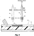
Fig. 5 is a schematic view of the PCB shown inFig. 5 , wherein the area in need of repair is recoated utilizing the nozzle assembly. - The subject invention is directed to a new and useful method for reworking or otherwise repairing a printed circuit board (PCB), an example of which is illustrated schematically in
Fig. 1 and designated generally byreference numeral 10. PCB 10 has an initialconformal coating 12 on all of the surfaces thereof, including on the surfaces of the components included thereon. - The
initial coating 12 is preferably a Parylene coating, and more preferably, theinitial coating 12 is an ultra-thin Parylene C coating, which has a useful combination of electrical and physical properties, plus very low permeability to moisture and corrosive gases. Alternatively, the initial coating could be an acrylic coating or a urethane coating, as is known in the art. Additional environmentally stable coatings are also contemplated. - The method of the subject invention includes the step of locally removing the
initial coating 12 from the surface of thePCB 10 at least in an area in need ofrepair 14, as illustrated schematically inFig. 2 . This can be accomplished in different ways and by different means. For example, it is envisioned that the step of removing theinitial coating 12 at least in thearea 14 of thePCB 10 that is in need of repair could involve mechanical removal by way of rubbing, abrading or stripping using specialized media blasting. Alternatively, the step of removing theinitial coating 12 could involve chemical removal using chemical stripping agents. It is also envisioned that the step of removing theinitial coating 12 could involve the interaction of external energy (e.g., laser, radiation or a plasma beam) with the coating material so that the coating would be selectively removed from the PCB. Those skilled in the art will readily appreciate that the optimal coating removal technique employed will typically depend upon the type of coating to be removed from the PCB. - The method of the subject invention further includes the step of recoating at least the
area 14 of thePCB 10 that is in need of repair, as illustrated schematically inFig. 3 . In accordance with a preferred embodiment of the subject invention, the step of recoating the PCB shown inFig. 3 is accomplished by way of atomic layer deposition (ALD), including plasma enhanced or thermal ALD. - ALD is a thin-film deposition technique that is based on the sequential use of a gas phase chemical process. The majority of ALD reactions use two chemicals, typically called precursors. These precursors react with the surface of a material one at a time in a sequential, self-limiting manner. Through repeated cyclic exposure to separate precursors, a thin film is slowly deposited. This ensures absolute thickness control, extreme layer homogeneity nominally without porosity or pinholes and superb conformity, even of high aspect ratio surfaces often found on a PCB.
- Preferably, the step of recoating at least the
area 14 of thePCB 10 that is in need of repair by way of ALD involves recoating thePCB 10 withnanolaminates 16 composed of a metal oxide. For example, the step of recoating at least thearea 14 of thePCB 10 that is in need of repair involves recoating thesurface area 14 of thePCB 10 with nanolaminates composed of an aluminum oxide (Al2O3) and titanium dioxide (TiO2) composition. Those skilled in the art will readily appreciate that other types of ALD coatings can be employed, such as for example coatings of silicon dioxide (SiO2) compositions or the like. Other coating architectures and compositions are also contemplated. In one example, the coating deposited in the recoating step consists of a layer with nominally a single composition. In other examples, the coatings deposited in the recoating step consist of two or more alternating layers with different compositions and different or nominally a single composition 'doped' with a second composition. Other ceramic, organic and hybrid-inorganic coating options are also contemplated. - It is envisioned that the method of the subject invention would also include the step of masking the surface of the
PCB 10 to isolate at least the area that is in need of repair for recoating. It is also envisioned that the method of the subject invention could include the step of preparing the surface of the PCB at least in the area in need of repair for recoating. This step could be accomplished by way of a plasma process, a chemical pretreatment or by other means known in the art. - It is envisioned that the step of recoating at least the area of the
PCB 10 in need of repair could involve either spatial or localized ALD. Those skilled in the art will readily appreciate that spatial ALD is an enhanced form of traditional ALD, improving the deposition rate by several orders of magnitude. Moreover, instead of filling and flushing a process chamber repeatedly, spatial ALD uses a multitude of precursor zones through which the substrates pass at high speed. Gas bearing and exhaust slits in between the precursor zones, keep the precursors from mixing avoiding parasitic deposition. - It is envisioned that the step of recoating the
PCB 10 could involve utilizing a localized energy source delivered through anozzle assembly 18, as illustrated for example schematically inFig, 4 . Thenozzle assembly 18 would preferably include an elongated tubular body with an outer diameter of about 0.25 inches, and having an energizingcoil 22 provided on a distal end portion thereof (e.g., a radio frequency coil), a first inlet for receiving a plasma gas (e.g., Oxygen, Argon or Helium), a second inlet for receiving an alternate gas (e.g., an inert purge gas such as argon or nitrogen), and a deposition source inlet for receiving the metal oxide composition to be deposited by the nozzle through ALD. An example of such an assembly is disclosed in commonly assignedU.S. Patent Application Publication 2019/0037678 , the disclosure of which is herein incorporated by reference in its entirety. - The
nozzle assembly 18 could also be used to remove theinitial coating 12 from the area of thePCB 10 that is in need of repair. That is thenozzle assembly 18 could generate a cleaning plasma beam to locally remove or otherwise volatilize theinitial coating 12 in the area of thePCB 10 that is in need of repair. Various nozzle assemblies (tube, plate, slot, etc.) with single or multiple nozzle configurations are contemplated. - The method would further involve the step of moving the
nozzle assembly 18 relative to thePCB 10 by way of amulti-axis maneuvering system 20, as shown for example inFig, 5 . Alternatively, thePCB 10 could be moved relative to thenozzle assembly 18 by placing the PCB on a multi-axis working surface (not shown). - It is envisioned that the step of recoating at least the area of the
PCB 10 in need of repair would involve depositing a coating by way of atomic layer deposition that has a thickness of about 50 nanometers (nm) to about 1 micron (µ), and more preferably, a thickness of 50 - 100 nm. It is further envisioned that the method could involve recoating the entire surface of the PCB by way of atomic layer deposition, rather than just recoating the area of the PCB in need of repair. - It has been determined through experimentation that a PCB having an initial coating of Parylene C, that has been mechanically removed and recoated with nanolaminates composed of an aluminum oxide (Al2O3) and titanium dioxide (TiO2) in accordance with the method of the subject invention possesses favorable properties such as moisture and insulation resistance (MIR), hydrolytic stability, mechanical flexibility and dielectric barrier.
- While the subject disclosure has been shown and described with reference to preferred embodiments, those skilled in the art will readily appreciate that changes and/or modifications may be made thereto without departing from the scope of the subject disclosure.
Claims (15)
- A method for repairing a printed circuit board (PCB) comprising:a) presenting a PCB (10) having an initial coating (12) on a surface thereof;b) removing the initial coating (12) from the surface of the PCB (10) at least in an area in need of repair; andc) recoating at least the area of the PCB (10) in need of repair by way of atomic layer deposition.
- A method for repairing a printed circuit board (PCB) according to Claim 1, wherein the step of recoating at least the area of the PCB (10) in need of repair involves recoating with nanolaminates composed of a metal oxide.
- A method for repairing a printed circuit board (PCB) according to Claim 1, wherein the step of recoating at least the area of the PCB in need of repair involves recoating with nanolaminates composed of an aluminum oxide (Al2O3) and titanium dioxide (TiO2) composition.
- A method for repairing a printed circuit board (PCB) according to any preceding claim, wherein the initial coating is a parylene coating, an acrylic coating or a urethane coating.
- A method for repairing a printed circuit board (PCB) according to any preceding claim, further comprising the step of masking the surface of the PCB (10) to isolate at least the area in need of repair for recoating.
- A method for repairing a printed circuit board (PCB) according to any preceding claim 1, further comprising the step of preparing the surface of the PCB (10) at least in the area in need of repair for recoating by way of a plasma process.
- A method for repairing a printed circuit board (PCB) according to any preceding claim, wherein the step of removing the initial coating at least in the area in need of repair involves mechanical, chemical or external energy based removal techniques.
- A method for repairing a printed circuit board (PCB) according to any preceding claim, wherein the step of recoating at least the area of the PCB (10) in need of repair involves plasma enhanced or thermal atomic layer deposition.
- A method for repairing a printed circuit board (PCB) according to any of claims 1 to 8, wherein the step of recoating at least the area of the PCB (10) in need of repair involves spatial or localized atomic layer deposition.
- A method for repairing a printed circuit board (PCB) according to any of claims 1 to 8, wherein at least the step of recoating the PCB (10) involves utilizing a localized energy source delivered through a nozzle assembly (18).
- A method for repairing a printed circuit board (PCB) according to Claim 10, further comprising the step of moving the nozzle assembly (18) relative to the PCB (10).
- A method for repairing a printed circuit board (PCB) according to any preceding claim, further comprising the step of moving the PCB (10) relative to the nozzle assembly.
- A method for repairing a printed circuit board (PCB) according to any preceding claim, wherein the step of removing the initial coating from the surface of the PCB (10) and the step of recoating the PCB (10) involves utilizing a localized energy source delivered through a nozzle assembly.
- A method for repairing a printed circuit board (PCB) according to any preceding claim, wherein the step of recoating at least the area of the PCB (10) in need of repair involves depositing a coating having a thickness of 50 nm to 1 µ.
- A method for repairing a printed circuit board (PCB) according to any preceding claim, comprising recoating the entire surface of the PCB (10) by way of atomic layer deposition.
Applications Claiming Priority (1)
| Application Number | Priority Date | Filing Date | Title |
|---|---|---|---|
| US16/270,383 US20200260592A1 (en) | 2019-02-07 | 2019-02-07 | Method for repairing coated printed circuit boards |
Publications (2)
| Publication Number | Publication Date |
|---|---|
| EP3694297A2 true EP3694297A2 (en) | 2020-08-12 |
| EP3694297A3 EP3694297A3 (en) | 2020-12-09 |
Family
ID=68653302
Family Applications (1)
| Application Number | Title | Priority Date | Filing Date |
|---|---|---|---|
| EP19210326.5A Pending EP3694297A3 (en) | 2019-02-07 | 2019-11-20 | Method for repairing coated printed circuit boards |
Country Status (2)
| Country | Link |
|---|---|
| US (1) | US20200260592A1 (en) |
| EP (1) | EP3694297A3 (en) |
Citations (1)
| Publication number | Priority date | Publication date | Assignee | Title |
|---|---|---|---|---|
| US20190037678A1 (en) | 2017-07-28 | 2019-01-31 | United Technologies Corporation | Method for additively manufacturing components |
Family Cites Families (5)
| Publication number | Priority date | Publication date | Assignee | Title |
|---|---|---|---|---|
| AT412719B (en) * | 2003-06-16 | 2005-06-27 | Eckelt Glas Gmbh | METHOD AND DEVICE FOR PROCESSING DEFLECTING GLASS PANELS |
| US20130323422A1 (en) * | 2012-05-29 | 2013-12-05 | Applied Materials, Inc. | Apparatus for CVD and ALD with an Elongate Nozzle and Methods Of Use |
| US9894776B2 (en) * | 2013-01-08 | 2018-02-13 | Hzo, Inc. | System for refurbishing or remanufacturing an electronic device |
| KR101715223B1 (en) * | 2015-05-15 | 2017-03-14 | 고려대학교 산학협력단 | Apparatus for selectively depositing atomic layer for local area on the substrate |
| KR102586409B1 (en) * | 2016-04-12 | 2023-10-11 | 피코순 오와이 | Coating by ALD to suppress metal whiskers |
-
2019
- 2019-02-07 US US16/270,383 patent/US20200260592A1/en not_active Abandoned
- 2019-11-20 EP EP19210326.5A patent/EP3694297A3/en active Pending
Patent Citations (1)
| Publication number | Priority date | Publication date | Assignee | Title |
|---|---|---|---|---|
| US20190037678A1 (en) | 2017-07-28 | 2019-01-31 | United Technologies Corporation | Method for additively manufacturing components |
Also Published As
| Publication number | Publication date |
|---|---|
| EP3694297A3 (en) | 2020-12-09 |
| US20200260592A1 (en) | 2020-08-13 |
Similar Documents
| Publication | Publication Date | Title |
|---|---|---|
| US11387107B2 (en) | Deposition of organic films | |
| KR102308849B1 (en) | Non-line of sight deposition of erbium based plasma resistant ceramic coating | |
| KR20220041797A (en) | Selective deposition using hydrophobic precursors | |
| CN109314058A (en) | Articles and methods of forming vias in a substrate | |
| ATE265558T1 (en) | METHOD FOR PRODUCING A MULTI-LAYER OBJECT USING ARC PLASMA COATING | |
| JP2022180352A (en) | Chemical resistant multi-layer coating applied by atomic layer deposition | |
| US11421319B2 (en) | Plasma etch-resistant film and a method for its fabrication | |
| TWI799377B (en) | A deposition method carried out in a reactor system, use of the method and an ald reactor system | |
| CN113227435A (en) | Plasma resistant multilayer coating and method for making same | |
| JP2019522113A5 (en) | ||
| JP2003501555A (en) | Doped diamond-like carbon coating | |
| WO2006137541A1 (en) | Constitutional member for semiconductor processing apparatus and method for producing same | |
| US20110073236A1 (en) | High strength bonding and coating mixture | |
| KR101524271B1 (en) | A composition of anti-fingerprint coating layer with a plurality of thin films and method of manufacturing the same. | |
| US7351480B2 (en) | Tubular structures with coated interior surfaces | |
| US20200260592A1 (en) | Method for repairing coated printed circuit boards | |
| CN117062939A (en) | Metal oxyfluoride film formation method | |
| RU2392352C1 (en) | Procedure for application of metal coating on padding | |
| JP2969291B2 (en) | Abrasion resistant member and method of manufacturing the same | |
| KR20150087065A (en) | Method for cvd coating | |
| KR20040104227A (en) | Fabrication Method of Nano-tube Using Atomic Layer Deposition And Nano-template | |
| WO2023039425A1 (en) | Methods of forming a plasma resistant coating of y-o-f and substrates having such coating | |
| Naveed | Fundamentals of thin films | |
| WO2024227971A1 (en) | A plasma etch-resistant film and a method for its fabrication | |
| KR20090101610A (en) | A chemical resistance ceramics film |
Legal Events
| Date | Code | Title | Description |
|---|---|---|---|
| PUAI | Public reference made under article 153(3) epc to a published international application that has entered the european phase |
Free format text: ORIGINAL CODE: 0009012 |
|
| STAA | Information on the status of an ep patent application or granted ep patent |
Free format text: STATUS: THE APPLICATION HAS BEEN PUBLISHED |
|
| AK | Designated contracting states |
Kind code of ref document: A2 Designated state(s): AL AT BE BG CH CY CZ DE DK EE ES FI FR GB GR HR HU IE IS IT LI LT LU LV MC MK MT NL NO PL PT RO RS SE SI SK SM TR |
|
| AX | Request for extension of the european patent |
Extension state: BA ME |
|
| PUAL | Search report despatched |
Free format text: ORIGINAL CODE: 0009013 |
|
| AK | Designated contracting states |
Kind code of ref document: A3 Designated state(s): AL AT BE BG CH CY CZ DE DK EE ES FI FR GB GR HR HU IE IS IT LI LT LU LV MC MK MT NL NO PL PT RO RS SE SI SK SM TR |
|
| AX | Request for extension of the european patent |
Extension state: BA ME |
|
| RIC1 | Information provided on ipc code assigned before grant |
Ipc: H05K 3/22 20060101ALI20201105BHEP Ipc: C23C 28/04 20060101ALI20201105BHEP Ipc: H05K 3/28 20060101AFI20201105BHEP Ipc: C23C 16/455 20060101ALI20201105BHEP Ipc: C23C 16/02 20060101ALI20201105BHEP |
|
| STAA | Information on the status of an ep patent application or granted ep patent |
Free format text: STATUS: REQUEST FOR EXAMINATION WAS MADE |
|
| 17P | Request for examination filed |
Effective date: 20210609 |
|
| RBV | Designated contracting states (corrected) |
Designated state(s): AL AT BE BG CH CY CZ DE DK EE ES FI FR GB GR HR HU IE IS IT LI LT LU LV MC MK MT NL NO PL PT RO RS SE SI SK SM TR |
|
| STAA | Information on the status of an ep patent application or granted ep patent |
Free format text: STATUS: EXAMINATION IS IN PROGRESS |
|
| 17Q | First examination report despatched |
Effective date: 20250916 |