EP3694120B1 - Dynamic time constant for quick decision level acquisition - Google Patents
Dynamic time constant for quick decision level acquisition Download PDFInfo
- Publication number
- EP3694120B1 EP3694120B1 EP20155188.4A EP20155188A EP3694120B1 EP 3694120 B1 EP3694120 B1 EP 3694120B1 EP 20155188 A EP20155188 A EP 20155188A EP 3694120 B1 EP3694120 B1 EP 3694120B1
- Authority
- EP
- European Patent Office
- Prior art keywords
- circuit
- terminal
- coupled
- transistor
- offset
- Prior art date
- Legal status (The legal status is an assumption and is not a legal conclusion. Google has not performed a legal analysis and makes no representation as to the accuracy of the status listed.)
- Active
Links
Images




Classifications
-
- H—ELECTRICITY
- H03—ELECTRONIC CIRCUITRY
- H03K—PULSE TECHNIQUE
- H03K5/00—Manipulating of pulses not covered by one of the other main groups of this subclass
- H03K5/003—Changing the DC level
-
- H—ELECTRICITY
- H04—ELECTRIC COMMUNICATION TECHNIQUE
- H04B—TRANSMISSION
- H04B10/00—Transmission systems employing electromagnetic waves other than radio-waves, e.g. infrared, visible or ultraviolet light, or employing corpuscular radiation, e.g. quantum communication
- H04B10/60—Receivers
- H04B10/66—Non-coherent receivers, e.g. using direct detection
- H04B10/69—Electrical arrangements in the receiver
- H04B10/693—Arrangements for optimizing the preamplifier in the receiver
- H04B10/6933—Offset control of the differential preamplifier
-
- H—ELECTRICITY
- H04—ELECTRIC COMMUNICATION TECHNIQUE
- H04Q—SELECTING
- H04Q11/00—Selecting arrangements for multiplex systems
- H04Q11/0001—Selecting arrangements for multiplex systems using optical switching
- H04Q11/0062—Network aspects
- H04Q11/0067—Provisions for optical access or distribution networks, e.g. Gigabit Ethernet Passive Optical Network (GE-PON), ATM-based Passive Optical Network (A-PON), PON-Ring
-
- H—ELECTRICITY
- H04—ELECTRIC COMMUNICATION TECHNIQUE
- H04B—TRANSMISSION
- H04B10/00—Transmission systems employing electromagnetic waves other than radio-waves, e.g. infrared, visible or ultraviolet light, or employing corpuscular radiation, e.g. quantum communication
- H04B10/25—Arrangements specific to fibre transmission
-
- H—ELECTRICITY
- H04—ELECTRIC COMMUNICATION TECHNIQUE
- H04B—TRANSMISSION
- H04B10/00—Transmission systems employing electromagnetic waves other than radio-waves, e.g. infrared, visible or ultraviolet light, or employing corpuscular radiation, e.g. quantum communication
- H04B10/27—Arrangements for networking
Definitions
- the present invention relates in general to a passive optical network and, more particularly, to a level acquisition circuit with a dynamic time constant.
- a gigabit passive optical network provides high speed data communications, over a fiber optical cable, between an internet service provider (ISP) and end user.
- ISP internet service provider
- a GPON uses point-to-multipoint architecture (1:32) or (1:64) with a fiber optic splitter to serve multiple end-points from a single optical source.
- the GPON includes an optical line terminal (OLT) at the ISP central office or switching center and a plurality of optical network units (ONU) or optical network terminals (ONT) located near the end users. Each ONU serves an individual end user.
- OLT optical line terminal
- ONU optical network units
- ONT optical network terminals
- Each ONU serves an individual end user.
- a GPON reduces the amount of fiber and central office equipment as compared with other networks since unpowered fiber optic splitters are used to enable a single optical fiber to serve multiple end-points.
- the GPON is a shared network, in that the OLT sends a stream of data packets as downstream traffic that is seen by all ONUs.
- the OLT transmitter and ONU receiver operate in continuous mode (CM).
- CM continuous mode
- Each ONU reads the content of the data packets that correspond to the particular ONU address. Encryption prevents eavesdropping on downstream traffic.
- the ONU typically cannot transmit the optical data signal in CM, because there are more ONUs than OLTs and the receive timing of the optical data signal is variable. Instead, signals are combined using a multiple access protocol, such time division multiple access (TDMA). Therefore, a given ONU transmits an optical packet in an assigned time slot using burst mode (BM) transmission. All ONUs use the same clock frequency as the OLT as they extract the frequency from the downstream channel by using a clock and data recovery (CDR) circuit.
- CDR clock and data recovery
- EP 1 791 276 A1 discloses a burst mode optical receiver that enables an optical receiver to receive signals from a plurality of optical network units at different optical power levels.
- US 2007/286611 A1 discloses a transimpedance amplifier (TIA) circuit usable for burst mode communications with a TIA stage, limiter-amplifier, and DC restoration loop.
- WO 2011/109770 A2 discloses an integrator circuit that cancels a DC offset component related to an average DC value of a burst mode input signal from the output of an amplifier by providing an average DC value of the input signal in a response time that is shorter than the preamble of a burst mode signal to maintain the integrator output signal stable within selected amplitude limits for a length of time corresponding to the data portion of a burst mode signal.
- US 2009/212839 discloses a circuit for settling DC offset and controlling RC time-constant in a direct conversion receiver.
- the DC offset settling circuit includes a node for receiving a bias voltage, a couple of input nodes for receiving a differential radio frequency signal pair, a couple of output nodes for outputting an output signal pair, a couple of resistors for protecting the DC offset settling circuit from overloading, two capacitors for adjusting logic level of the bias voltage, and a variable resistive unit for providing a variable resistance.
- a signal control unit can provide a control signal for determining an equivalent resistance of the variable resistive unit.
- the variable resistive unit can further include a FET transistor for providing a continuously variable resistance.
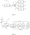
- FIG. 1 illustrates GPON 100 providing high speed data communications, over fiber optical cable, between an ISP and end users.
- GPON 100 includes OLT 102 located within the ISP home office or switching center.
- OLT 102 makes connection with the internet.
- OLT 102 is coupled through fiber optical cable 104 to optical splitter 106, which provides multiple optical signal paths through fiber optical cables 108 to ONU 110, 112, and 114 located near end users.
- optical splitter 106 connects up to 32 or 64 ONUs and brings optical fiber cabling and signals to the end user.
- GPON 100 is a shared network, in that OLT 102 sends a stream of data packets as downstream traffic through fiber optical cables 104 and 108 to ONU 110-114. Each ONU 110-114 reads the content of the data packets that correspond to the particular ONU address. Encryption prevents eavesdropping on downstream traffic.
- the ONU transmits the optical data signal using a multiple access protocol, such TDMA.
- a given ONU transmits an optical packet in an assigned time slot using BM transmission. All ONUs use the same clock frequency as the OLT as they extract the frequency from the downstream channel by using a CDR circuit.
- the present invention is also applicable to gigabit ethernet passive optical network (GEPON), EPON, 10G-EPON, XGPON, XGSPON, 25G-EPON, 50G-EPON, and other burst PON applications for sending data packets.
- GEPON gigabit ethernet passive optical network
- EPON EPON
- 10G-EPON 10G-EPON
- XGPON XGPON
- XGSPON 25G-EPON
- 50G-EPON 50G-EPON
- FIG. 2 illustrates further detail of the receiver portion of OLT 102, i.e., receiving the upstream optical data signal in bursts from ONU 110-114.
- Avalanche photodiode (APD) 120 detects the upstream optical data signal from ONU 110-114.
- the cathode of APD 120 is coupled to a positive power supply conductor 122, and the anode is coupled to an input of burst mode (BM) transimpedance amplifier (TIA) 124.
- APD 120 converts the optical data signal to current I APD .
- BM TIA 124 converts I APD to a voltage representative of the received optical data signal, and resistor 126 sets the gain of BM TIA 124.
- the differential output of BM TIA 124 is coupled to a differential input of level acquisition circuit 128.
- the differential output of level acquisition circuit 128 is coupled to a differential input of BM limiting amplifier (LIA) 130, and the differential output of BM LIA 130 is coupled to a differential input of BM CDR 132.
- GPON medium access control (MAC) 136 controls the communication between downstream data and upstream data. GPON MAC 136 generates RESET at each burst cycle to reset level acquisition circuit 128 and BM LIA 130.
- An upstream data signal 140 is received by APD 120 of OLT 102 in FIG. 3 .
- Time t 0 marks the end of a previous burst cycle 141.
- Guard interval 142 ensures that ONUs 110-114 do not interfere with one another, or otherwise cause overlapping transmissions.
- GPON MAC 136 generates RESET to prepare for processing the next burst of data.
- the incoming burst of data has an unknown amplitude that must be accommodated or compensated for.
- BM LIA 130 keeps asserted the signal detect SD from the previous burst.
- Signal detect SD is reset or cleared by RESET from the MAC 136.
- RESET may arrive from MAC 136 either during guard time interval 142 or during preamble 144.
- Preamble 144 begins at time t 1 with a sequence of one optical level followed by a zero optical level.
- Signal detect SD asserts at some point during preamble 144 and remains asserted until it is cleared by another RESET.
- BM TIA 124 and BM LIA 130 use the time period of preamble 144 to compensate for amplitude variation of data signal 140 and for BM 132 to phase-align with the transmitting ONU.
- the next data payload 146 begins at time t 2 .
- Guard time 142 and preamble 144 represent overhead of the communication protocol and should be short in duration, e.g., 25.7 nanosecond (ns) guard time and 35.4 ns preamble at 1.244 Gbps.
- BM TIA 124 handles a wide range of amplitude variations in data payload 146, i.e., the amplitude of the data signal may be high or low.
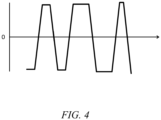
- the differential output signal of BM TIA 124 is symmetrical about a reference signal, such as 0.0 VDC, see FIG. 4 .
- a reference signal such as 0.0 VDC
- the optical signal from ONU 110 may be attenuated more or less than the optical signal from ONU 112 or 114.
- the optical signal from ONU 110 may have an amplitude greater than or less than the optical signal from ONU 112 or 114.
- data burst 141 has a greater amplitude as compared to data payload 146.
- the differential output signal of BM TIA 124 may have a non-zero DC offset with respect to the reference signal (0.0 VDC) that varies with the amplitude of the input optical signal.
- Level acquisition circuit 128 creates a dynamic time constant for each burst cycle to remove or compensate for the DC offset from the differential signal from BM TIA 124. Under present design standards, there is a short time to remove the DC offset.
- FIG. 5 shows further detail of level acquisition circuit 128.
- the differential signal from BM TIA 124 is applied to terminals 150 and 152 of level acquisition circuit 128.
- Capacitor 154 is coupled between terminal 150 and node 156, and capacitor 158 is coupled between terminal 152 and node 160.
- Switched resistance network 162 is coupled between node 156 and terminal 164. Terminal 164 receives a reference voltage V CM corresponding to the input common mode of BM LIA 130.
- the combination of capacitor 154 and switched resistance network 162 creates a first variable time constant for the differential signal.
- Switched resistance network 166 is coupled between node 160 and terminal 164.
- the combination of capacitor 158 and switched resistance network 166 creates a second variable time constant for the differential signal.
- Terminals 170 and 172 are coupled to BM LIA 130.
- Capacitors 154 and 158 are coupled in the signal path between terminals 150-152 and terminals 170-172 and will block the DC component (remove the DC offset) of data signal 140, given the proper dynamic time constants. In differential mode, the difference between voltages across capacitors 154 and 158 is the DC offset that will be removed during the dynamic time constants.
- Capacitor 154 is charged with a time constant T 1 equal to C 154 (capacitance of capacitor 154) * R 162 (total effective resistance of switched resistance network 162).
- Capacitor 158 is charged with a time constant T 2 equal to C 158 (capacitance of capacitor 158) * R 166 (total effective resistance of switched resistance network 166).
- the time constants T 1 and T 2 are dynamically changed during the acquisition of the offset.
- the dynamic time constants T 1 and T 2 involve setting or configuring switched resistance networks 162 and 166 each with a minimum value of resistance to compensate for a large proportion of the DC offset.
- the dynamic time constants T 1 and T 2 are minimum values.
- the DC offset decreases rapidly (maximum rate of decrease).
- Switched resistance networks 162 and 166 are then set to larger values, less than the maximum selectable value of R 162 and R 166 .
- the dynamic time constants T 1 and T 2 gradually increases as the DC offset rate of decrease begins to slow down to remove the pattern dependency. Switched resistance networks 162 and 166 are then set to even larger values, and the dynamic time constants T 1 and T 2 become even larger and the DC offset decreases.
- FIG. 6 illustrates further detail of switched resistance network 162.
- Resistor 180 is coupled between node 156 and the drain of transistor 182.
- the gate of transistor 182 is coupled to output 183 of control circuit 184, and the source of transistor 182 is coupled to terminal 164.
- Resistor 186 is coupled between node 156 and the drain of transistor 188.
- the gate of transistor 188 is coupled to output 189 of control circuit 184, and the source of transistor 188 is coupled to terminal 164.
- Resistor 190 is coupled between node 156 and the drain of transistor 192.
- the gate of transistor 192 is coupled to output 194 of control circuit 184, and the source of transistor 192 is coupled to terminal 164.
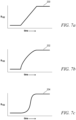
- FIG. 7a shows a resistance plot 200 of switched resistance network 162 monotonically increasing R 162 from a minimum value to a maximum value in a linear manner.
- FIG. 7b shows a resistance plot 202 of switched resistance network 162 monotonically increasing R 162 from a minimum value to a maximum value in a non-linear manner.
- FIG. 7c shows a resistance plot 204 of switched resistance network 162 monotonically increasing R 162 from a minimum value to a maximum value in another non-linear manner.
- the process can be reversed in that the switched resistance network 162 can be monotonically decreasing R 162 from a maximum to a minimum value.
- switched resistance network 162 can be selected from 5 ohms to 20k ohms with 5-10 levels of switched resistance.
- Capacitor 154 has a value of 30-80 picofarads (pF).
- switched resistance network 162 can be selected from 50 ohms to 800k ohms with 5 or more levels of switched resistance.
- Capacitor 154 has a value of 10-20 pF.
- Switched resistance network 166 follows a similar structure and operation. The monotonically increasing R 162 and R 166 , in combination with capacitors 154 and 158, create the dynamic time constants T 1 and T 2 to effectively remove the DC offset from differential signal 140 in a controlled manner and in a short time period, e.g., less than 25.7 ns.
- FIG. 8 illustrates an embodiment of level acquisition circuit 128 with variable capacitors 210 and 212, and variable drain-source resistance in a conductive state (RDSON) for transistors 214 and 216.
- Variable capacitors 210 and 212 can be implemented as a varactor.
- the differential signal from BM TIA 124 is applied to terminals 220 and 222 of level acquisition circuit 128.
- Variable capacitor 210 is coupled between terminal 220 and node 226, and variable capacitor 212 is coupled between terminal 222 and node 228.
- the drain of transistor 214 is coupled to node 226, and the source of transistor 214 is coupled to terminal 230.
- Terminal 230 receives a reference voltage V CM equal to the input common mode of BM LIA 130.
- the drain of transistor 216 is coupled to node 228, and the source of transistor 216 is coupled to terminal 230.
- Control circuit 232 provides output 234 to the gate of transistor 214 and output 236 to the gate of transistor 216.
- the combination of variable capacitor 210 and transistor 214 creates a first variable time constant for the differential signal.
- the combination of variable capacitor 212 and transistor 216 creates a second variable time constant for the differential signal.
- Terminals 240 and 242 are coupled to BM LIA 130.
- Capacitors 210 and 212 are coupled in the signal path between terminals 220-222 and 240-242 and will block the DC component (remove the DC offset) of data signal 140, given the proper dynamic time constants. In differential mode, the difference between voltages across capacitors 210 and 212 is the DC offset that will be removed during the dynamic time constant.
- Capacitor 210 is charged with a time constant T 1 equal to C 210 (variable capacitance of capacitor 210) * R 214 (RDSON of transistor 214).
- Capacitor 212 is charged with a time constant T 2 equal to C 212 (variable capacitance of capacitor 212) * R 216 (RDSON of transistor 216).
- the time constants T 1 and T 2 are dynamically changed during the acquisition of the offset. In this case, the values of C 210 , C 212 , R 214 , and R 216 can all be varied.
- the dynamic time constants involve setting variable capacitors 210 and 212, and setting RDSON of transistors 214 and 216 with a minimum value of resistance to compensate for a large proportion of the DC offset.
- the value of RDSON of transistors is a function of gate voltage from outputs 234 and 236 of control circuit 232.
- the dynamic time constants T 1 and T 2 are minimum values.
- the DC offset decreases rapidly (maximum rate of decrease).
- the RDSON of transistors 214 and 216 are then set to larger values, less than the maximum selectable value of R 214 and R 216 , by changing the gate voltage from outputs 234 and 236.
- the dynamic time constants T 1 and T 2 gradually increases as the DC offset rate of decrease begins to slow down to remove the pattern dependency.
- the RDSON of transistors 214 and 216 are then set to larger values, and the dynamic time constants T 1 and T 2 become even larger and the DC offset decreases.
- the process of monotonic increasing R 214 and R 216 , and corresponding increasing the dynamic time constants T 1 and T 2 continues as the DC offset correspondingly decreases.
- the RDSON of transistors 214 and 216 are set to maximum resistance, and the dynamic time constants T 1 and T 2 become maximum to remove the remaining DC offset.
- the dynamic time constants T 1 and T 2 effectively remove the DC offset from differential signal 140.
- FIG. 9a shows a gate voltage V GATE plot 250 transistor 214 monotonically increasing R 214 from a minimum value to a maximum value in a linear manner.
- FIG. 9b shows a gate voltage V GATE plot 252 of transistor 214 monotonically increasing R 214 from a minimum value to a maximum value in a non-linear manner.
- FIG. 9c shows a gate voltage V GATE plot 254 of transistor 214 monotonically increasing R 214 from a minimum value to a maximum value in another non-linear manner.
- FIG. 10 shows another embodiment of level acquisition circuit 128.
- the differential signal from BM TIA 124 is applied to terminals 260 and 262 of level acquisition circuit 128.
- Capacitor 264 is coupled between terminal 260 and node 266, and capacitor 268 is coupled between terminal 262 and node 270.
- Resistor digital to analog converter (RDAC) 272 is coupled between node 266 and terminal 274.
- Terminal 274 receives a reference voltage V CM equal to the input common mode of BM LIA 130.
- the combination of capacitor 264 and RDAC 272 creates a first variable time constant for the differential signal.
- RDAC 276 is coupled between node 270 and terminal 274.
- the combination of capacitor 268 and RDAC 276 creates a second variable time constant for the differential signal.
- Terminals 280 and 282 are coupled to BM LIA 130.
- Capacitors 264 and 268 are coupled in the signal path between terminals 260-262 and terminals 280-282 and will block the DC component (remove the DC offset) of data signal 140, given the proper dynamic time constants.
- Capacitor 264 is charged with a time constant T 1 equal to C 264 (capacitance of capacitor 264) * R 272 (total effective resistance of RDAC 272).
- Capacitor 268 is charged with a time constant T 2 equal to C 268 (capacitance of capacitor 268) * R 276 (total effective resistance of RDAC 276).
- the time constants T 1 and T 2 are dynamically changed during the acquisition of the offset.
- the dynamic time constants T 1 and T 2 involve setting or configuring RDAC 272 and 276 each with a minimum value of resistance to compensate for a large proportion of the DC offset.
- the dynamic time constants T 1 and T 2 are minimum values.
- the DC offset decreases rapidly (maximum rate of decrease).
- RDAC 272 and 276 are then set to larger values, less than the maximum selectable value of R 272 and R 276 .
- the dynamic time constants T 1 and T 2 gradually increases as the DC offset rate of decrease begins to slow down to remove the pattern dependency.
- RDAC 272 and 276 are then set to even larger values, and the dynamic time constants T 1 and T 2 become even larger and the DC offset decreases.
- FIG. 11 illustrates further detail of RDAC 272.
- Resistor 290 is coupled between node 266 and the drain of transistor 292.
- Resistor 294 is coupled between node 266 and the drain of transistor 296.
- Resistor 298 is coupled between node 266 and the drain of transistor 300.
- Resistor 302 is coupled between node 266 and the drain of transistor 304.
- the gate of transistor 292 is coupled to output 312 of control circuit 310, and the source of transistor 292 is coupled to terminal 274.
- the gate of transistor 296 is coupled to output 314 of control circuit 310, and the source of transistor 296 is coupled to terminal 274.
- the gate of transistor 300 is coupled to output 316 of control circuit 310, and the source of transistor 300 is coupled to terminal 274.
- the gate of transistor 304 is coupled to output 318 of control circuit 310, and the source of transistor 304 is coupled to terminal 274. Additional combinations of resistors and transistor can be connected between node 266 and terminal 274 to increase resolution of RDAC
- R 272 is the parallel combination of those resistors 290, 294, 298, and 302 having respective conducting transistors.
- Resistor 290 is largest value
- resistor 294 is smaller than resistor 290
- resistor 298 is smaller than resistor 294, and resistor 302 is the smallest value.
- the value of resistor 290 is R/2 0
- resistor 294 is R/2 1
- resistor 298 is R/2 N-1
- resistor 302 is R/2 N , where N is the number of resistors in the network.
- Outputs 312-318 are controlled by bit 0, bit 1, bit N-1, and bit N of RDAC 272. Additional resistors and transistors combinations can be connected and controlled, as described above, for more levels of switched resistance.
- RDAC 276 follows a similar structure and operation.
- level acquisition circuit 128 cancels or removes a large DC offset from differential signal 140 from BM TIA 124 during preamble 144 by varying the dynamic time constants of an RC circuit, without adding any penalty in terms of jitter even from the onset of the burst which improves the throughput and efficiency of OLT 102.
- the dynamic time constants can be tuned to optimize the residual voltage ripple across the capacitor and resulting jitter.
Landscapes
- Engineering & Computer Science (AREA)
- Physics & Mathematics (AREA)
- Computer Networks & Wireless Communication (AREA)
- Electromagnetism (AREA)
- Signal Processing (AREA)
- Nonlinear Science (AREA)
- Computing Systems (AREA)
- Amplifiers (AREA)
- Dc Digital Transmission (AREA)
Description
- The present invention relates in general to a passive optical network and, more particularly, to a level acquisition circuit with a dynamic time constant.
- A gigabit passive optical network (GPON) provides high speed data communications, over a fiber optical cable, between an internet service provider (ISP) and end user. A GPON uses point-to-multipoint architecture (1:32) or (1:64) with a fiber optic splitter to serve multiple end-points from a single optical source. For example, the GPON includes an optical line terminal (OLT) at the ISP central office or switching center and a plurality of optical network units (ONU) or optical network terminals (ONT) located near the end users. Each ONU serves an individual end user. A GPON reduces the amount of fiber and central office equipment as compared with other networks since unpowered fiber optic splitters are used to enable a single optical fiber to serve multiple end-points.
- The GPON is a shared network, in that the OLT sends a stream of data packets as downstream traffic that is seen by all ONUs. The OLT transmitter and ONU receiver operate in continuous mode (CM). Each ONU reads the content of the data packets that correspond to the particular ONU address. Encryption prevents eavesdropping on downstream traffic. However, in the upstream channel, the ONU typically cannot transmit the optical data signal in CM, because there are more ONUs than OLTs and the receive timing of the optical data signal is variable. Instead, signals are combined using a multiple access protocol, such time division multiple access (TDMA). Therefore, a given ONU transmits an optical packet in an assigned time slot using burst mode (BM) transmission. All ONUs use the same clock frequency as the OLT as they extract the frequency from the downstream channel by using a clock and data recovery (CDR) circuit.
- Many ONUs are geographically dispersed and operate at least partially out-of-phase because of the distance and delay to the OLT. The optical signals from different ONUs also experience different attenuation. Accordingly, the OLT receives BM optical packages from different ONUs that are asynchronous, out-of-phase, and with different amplitudes. The OLT must compensate for signal degradation, such as DC offset, from the phase and amplitude variation of the optical signal.
EP 1 791 276 A1 discloses a burst mode optical receiver that enables an optical receiver to receive signals from a plurality of optical network units at different optical power levels.
US 2007/286611 A1 discloses a transimpedance amplifier (TIA) circuit usable for burst mode communications with a TIA stage, limiter-amplifier, and DC restoration loop.
WO 2011/109770 A2 discloses an integrator circuit that cancels a DC offset component related to an average DC value of a burst mode input signal from the output of an amplifier by providing an average DC value of the input signal in a response time that is shorter than the preamble of a burst mode signal to maintain the integrator output signal stable within selected amplitude limits for a length of time corresponding to the data portion of a burst mode signal.
US 2009/212839 discloses a circuit for settling DC offset and controlling RC time-constant in a direct conversion receiver. The DC offset settling circuit includes a node for receiving a bias voltage, a couple of input nodes for receiving a differential radio frequency signal pair, a couple of output nodes for outputting an output signal pair, a couple of resistors for protecting the DC offset settling circuit from overloading, two capacitors for adjusting logic level of the bias voltage, and a variable resistive unit for providing a variable resistance. A signal control unit can provide a control signal for determining an equivalent resistance of the variable resistive unit. The variable resistive unit can further include a FET transistor for providing a continuously variable resistance. - It is therefore the object of the invention to provide an improved circuit for controlling a circuit time constant to achieve a substantially zero DC offset, as well as a method of making a corresponding circuit.
- This object is solved by the subject matter of the independent claims. Preferred embodiments are defined by the dependent claims.
-
FIG. 1 illustrates a gigabit passive optical network with OLT, optical splitter, and a plurality of ONUs; -
FIG. 2 illustrates further detail of the OLT of the GPON; -
FIG. 3 illustrates a timing diagram of a received data signal and control signals; -
FIG. 4 illustrates the differential output signal of the BM TIA symmetrical about a zero reference signal; -
FIG. 5 illustrates further detail of the level acquisition circuit in the OLT; -
FIG. 6 illustrates further detail of the switched resistance network in the level acquisition circuit ofFIG. 5 ; -
FIGs. 7a-7c illustrate linear and non-linear control of the switched resistance network inFIG. 6 ; -
FIG. 8 illustrates an embodiment of the switched resistance network in the level acquisition circuit; -
FIGs. 9a-9c illustrate linear and non-linear control of the switched resistance network inFIG. 8 ; -
FIG. 10 illustrates another example of the level acquisition circuit; and -
FIG. 11 illustrates further detail of the RDAC in the level acquisition circuit ofFIG. 10 . - The present invention is described in one or more embodiments in the following description with reference to the figures, in which like numerals represent the same or similar elements. While the invention is described in terms of the best mode for achieving the invention's objectives, those skilled in the art will appreciate that the description is intended to cover alternatives, modifications, and equivalents as may be included within the scope of the invention as defined by the appended claims.
-
FIG. 1 illustrates GPON 100 providing high speed data communications, over fiber optical cable, between an ISP and end users. GPON 100 includes OLT 102 located within the ISP home office or switching center. OLT 102 makes connection with the internet. OLT 102 is coupled through fiberoptical cable 104 tooptical splitter 106, which provides multiple optical signal paths through fiberoptical cables 108 to ONU 110, 112, and 114 located near end users. In one example,optical splitter 106 connects up to 32 or 64 ONUs and brings optical fiber cabling and signals to the end user. - GPON 100 is a shared network, in that OLT 102 sends a stream of data packets as downstream traffic through fiber
optical cables - The present invention is also applicable to gigabit ethernet passive optical network (GEPON), EPON, 10G-EPON, XGPON, XGSPON, 25G-EPON, 50G-EPON, and other burst PON applications for sending data packets.
-
FIG. 2 illustrates further detail of the receiver portion ofOLT 102, i.e., receiving the upstream optical data signal in bursts from ONU 110-114. Avalanche photodiode (APD) 120 detects the upstream optical data signal from ONU 110-114. The cathode ofAPD 120 is coupled to a positivepower supply conductor 122, and the anode is coupled to an input of burst mode (BM) transimpedance amplifier (TIA) 124.APD 120 converts the optical data signal to current IAPD. BM TIA 124 converts IAPD to a voltage representative of the received optical data signal, andresistor 126 sets the gain of BM TIA 124. The differential output of BM TIA 124 is coupled to a differential input oflevel acquisition circuit 128. The differential output oflevel acquisition circuit 128 is coupled to a differential input of BM limiting amplifier (LIA) 130, and the differential output of BM LIA 130 is coupled to a differential input ofBM CDR 132. GPON medium access control (MAC) 136 controls the communication between downstream data and upstream data.GPON MAC 136 generates RESET at each burst cycle to resetlevel acquisition circuit 128 andBM LIA 130. - An upstream data signal 140 is received by
APD 120 ofOLT 102 inFIG. 3 . Time t0 marks the end of aprevious burst cycle 141.Guard interval 142 ensures that ONUs 110-114 do not interfere with one another, or otherwise cause overlapping transmissions. Duringguard interval 142,GPON MAC 136 generates RESET to prepare for processing the next burst of data. The incoming burst of data has an unknown amplitude that must be accommodated or compensated for.BM LIA 130 keeps asserted the signal detect SD from the previous burst. Signal detect SD is reset or cleared by RESET from theMAC 136. RESET may arrive fromMAC 136 either duringguard time interval 142 or duringpreamble 144.Preamble 144 begins at time t1 with a sequence of one optical level followed by a zero optical level. Signal detect SD asserts at some point duringpreamble 144 and remains asserted until it is cleared by another RESET.BM TIA 124 andBM LIA 130 use the time period ofpreamble 144 to compensate for amplitude variation of data signal 140 and forBM 132 to phase-align with the transmitting ONU. Thenext data payload 146 begins at time t2.Guard time 142 andpreamble 144 represent overhead of the communication protocol and should be short in duration, e.g., 25.7 nanosecond (ns) guard time and 35.4 ns preamble at 1.244 Gbps. -
BM TIA 124 handles a wide range of amplitude variations indata payload 146, i.e., the amplitude of the data signal may be high or low. In the ideal case, the differential output signal ofBM TIA 124 is symmetrical about a reference signal, such as 0.0 VDC, seeFIG. 4 . When the differential signal swings around a different voltage, that voltage difference to the ideal zero level is a DC offset. There should be no DC offset of the differential signal with respect to the reference signal (0.0 VDC). However, the optical signal fromONU 110 may be attenuated more or less than the optical signal fromONU ONU 110 may have an amplitude greater than or less than the optical signal fromONU data payload 146. Due to such system variation, e.g., changes in optical signal amplitude from one burst to another burst, as well as variations in delay from ONU 110-114 toOLT 102, the differential output signal ofBM TIA 124 may have a non-zero DC offset with respect to the reference signal (0.0 VDC) that varies with the amplitude of the input optical signal.Level acquisition circuit 128 creates a dynamic time constant for each burst cycle to remove or compensate for the DC offset from the differential signal fromBM TIA 124. Under present design standards, there is a short time to remove the DC offset. -
FIG. 5 shows further detail oflevel acquisition circuit 128. The differential signal fromBM TIA 124 is applied toterminals 150 and 152 oflevel acquisition circuit 128.Capacitor 154 is coupled betweenterminal 150 andnode 156, andcapacitor 158 is coupled between terminal 152 andnode 160. Switchedresistance network 162 is coupled betweennode 156 andterminal 164.Terminal 164 receives a reference voltage VCM corresponding to the input common mode ofBM LIA 130. The combination ofcapacitor 154 and switchedresistance network 162 creates a first variable time constant for the differential signal. Switchedresistance network 166 is coupled betweennode 160 andterminal 164. The combination ofcapacitor 158 and switchedresistance network 166 creates a second variable time constant for the differential signal.Terminals BM LIA 130.Capacitors capacitors -
Capacitor 154 is charged with a time constant T1 equal to C154 (capacitance of capacitor 154) * R162 (total effective resistance of switched resistance network 162).Capacitor 158 is charged with a time constant T2 equal to C158 (capacitance of capacitor 158) * R166 (total effective resistance of switched resistance network 166). To remove or compensate for the DC offset from the differential signal, the time constants T1 and T2 are dynamically changed during the acquisition of the offset. - The dynamic time constants T1 and T2 involve setting or configuring switched
resistance networks resistance networks resistance networks resistance networks differential signal 140 in a controlled manner and in a short time period, e.g., less than 25.7 ns for GPON. -
FIG. 6 illustrates further detail of switchedresistance network 162.Resistor 180 is coupled betweennode 156 and the drain oftransistor 182. The gate oftransistor 182 is coupled tooutput 183 ofcontrol circuit 184, and the source oftransistor 182 is coupled toterminal 164.Resistor 186 is coupled betweennode 156 and the drain oftransistor 188. The gate oftransistor 188 is coupled tooutput 189 ofcontrol circuit 184, and the source oftransistor 188 is coupled toterminal 164.Resistor 190 is coupled betweennode 156 and the drain oftransistor 192. The gate oftransistor 192 is coupled tooutput 194 ofcontrol circuit 184, and the source oftransistor 192 is coupled toterminal 164. - In
FIG. 6 , R162 is the parallel combination of thoseresistors Resistor 180 is smallest value,resistor 186 is a midrange value, andresistor 190 is the largest value. For minimum R162,output transistors output 183 is low andoutputs transistor 182 is non-conductive andtransistors output 194 is high,transistors transistor 192 is conductive, and R162 = R190. Additional resistors and transistors combinations can be connected and controlled, as described above, for more levels of switched resistance. Switchedresistance network 166 follows a similar structure and operation. -
FIG. 7a shows aresistance plot 200 of switchedresistance network 162 monotonically increasing R162 from a minimum value to a maximum value in a linear manner.FIG. 7b shows aresistance plot 202 of switchedresistance network 162 monotonically increasing R162 from a minimum value to a maximum value in a non-linear manner.FIG. 7c shows aresistance plot 204 of switchedresistance network 162 monotonically increasing R162 from a minimum value to a maximum value in another non-linear manner. The process can be reversed in that the switchedresistance network 162 can be monotonically decreasing R162 from a maximum to a minimum value. In one example, switchedresistance network 162 can be selected from 5 ohms to 20k ohms with 5-10 levels of switched resistance.Capacitor 154 has a value of 30-80 picofarads (pF). Alternatively, switchedresistance network 162 can be selected from 50 ohms to 800k ohms with 5 or more levels of switched resistance.Capacitor 154 has a value of 10-20 pF. Switchedresistance network 166 follows a similar structure and operation. The monotonically increasing R162 and R166, in combination withcapacitors differential signal 140 in a controlled manner and in a short time period, e.g., less than 25.7 ns. -
FIG. 8 illustrates an embodiment oflevel acquisition circuit 128 withvariable capacitors transistors Variable capacitors BM TIA 124 is applied toterminals level acquisition circuit 128.Variable capacitor 210 is coupled betweenterminal 220 andnode 226, andvariable capacitor 212 is coupled betweenterminal 222 andnode 228. The drain oftransistor 214 is coupled tonode 226, and the source oftransistor 214 is coupled toterminal 230.Terminal 230 receives a reference voltage VCM equal to the input common mode ofBM LIA 130. The drain oftransistor 216 is coupled tonode 228, and the source oftransistor 216 is coupled toterminal 230.Control circuit 232 providesoutput 234 to the gate oftransistor 214 andoutput 236 to the gate oftransistor 216. The combination ofvariable capacitor 210 andtransistor 214 creates a first variable time constant for the differential signal. The combination ofvariable capacitor 212 andtransistor 216 creates a second variable time constant for the differential signal.Terminals BM LIA 130.Capacitors capacitors -
Capacitor 210 is charged with a time constant T1 equal to C210 (variable capacitance of capacitor 210) * R214 (RDSON of transistor 214).Capacitor 212 is charged with a time constant T2 equal to C212 (variable capacitance of capacitor 212) * R216 (RDSON of transistor 216). To remove or compensate for the DC offset from the differential signal, the time constants T1 and T2 are dynamically changed during the acquisition of the offset. In this case, the values of C210, C212, R214, and R216 can all be varied. - The dynamic time constants involve setting
variable capacitors transistors outputs control circuit 232. The dynamic time constants T1 and T2 are minimum values. The DC offset decreases rapidly (maximum rate of decrease). The RDSON oftransistors outputs transistors transistors differential signal 140. -
FIG. 9a shows a gate voltage VGATE plot 250transistor 214 monotonically increasing R214 from a minimum value to a maximum value in a linear manner.FIG. 9b shows a gate voltage VGATE plot 252 oftransistor 214 monotonically increasing R214 from a minimum value to a maximum value in a non-linear manner.FIG. 9c shows a gate voltage VGATE plot 254 oftransistor 214 monotonically increasing R214 from a minimum value to a maximum value in another non-linear manner. -
FIG. 10 shows another embodiment oflevel acquisition circuit 128. The differential signal fromBM TIA 124 is applied toterminals level acquisition circuit 128.Capacitor 264 is coupled betweenterminal 260 andnode 266, andcapacitor 268 is coupled betweenterminal 262 andnode 270. Resistor digital to analog converter (RDAC) 272 is coupled betweennode 266 andterminal 274.Terminal 274 receives a reference voltage VCM equal to the input common mode ofBM LIA 130. The combination ofcapacitor 264 andRDAC 272 creates a first variable time constant for the differential signal.RDAC 276 is coupled betweennode 270 andterminal 274. The combination ofcapacitor 268 andRDAC 276 creates a second variable time constant for the differential signal.Terminals BM LIA 130.Capacitors -
Capacitor 264 is charged with a time constant T1 equal to C264 (capacitance of capacitor 264) * R272 (total effective resistance of RDAC 272).Capacitor 268 is charged with a time constant T2 equal to C268 (capacitance of capacitor 268) * R276 (total effective resistance of RDAC 276). To remove or compensate for the DC offset from the differential signal, the time constants T1 and T2 are dynamically changed during the acquisition of the offset. - The dynamic time constants T1 and T2 involve setting or configuring
RDAC RDAC RDAC RDAC differential signal 140. -
FIG. 11 illustrates further detail ofRDAC 272.Resistor 290 is coupled betweennode 266 and the drain oftransistor 292.Resistor 294 is coupled betweennode 266 and the drain oftransistor 296.Resistor 298 is coupled betweennode 266 and the drain oftransistor 300.Resistor 302 is coupled betweennode 266 and the drain oftransistor 304. The gate oftransistor 292 is coupled tooutput 312 ofcontrol circuit 310, and the source oftransistor 292 is coupled toterminal 274. The gate oftransistor 296 is coupled tooutput 314 ofcontrol circuit 310, and the source oftransistor 296 is coupled toterminal 274. The gate oftransistor 300 is coupled tooutput 316 ofcontrol circuit 310, and the source oftransistor 300 is coupled toterminal 274. The gate oftransistor 304 is coupled tooutput 318 ofcontrol circuit 310, and the source oftransistor 304 is coupled toterminal 274. Additional combinations of resistors and transistor can be connected betweennode 266 and terminal 274 to increase resolution ofRDAC 272. - In
FIG. 11 , R272 is the parallel combination of thoseresistors Resistor 290 is largest value,resistor 294 is smaller thanresistor 290,resistor 298 is smaller thanresistor 294, andresistor 302 is the smallest value. In one example, the value ofresistor 290 is R/20,resistor 294 is R/21,resistor 298 is R/2N-1, andresistor 302 is R/2N, where N is the number of resistors in the network. Outputs 312-318 are controlled bybit 0, bit 1, bit N-1, and bit N ofRDAC 272. Additional resistors and transistors combinations can be connected and controlled, as described above, for more levels of switched resistance.RDAC 276 follows a similar structure and operation. - In summary,
level acquisition circuit 128 cancels or removes a large DC offset fromdifferential signal 140 fromBM TIA 124 duringpreamble 144 by varying the dynamic time constants of an RC circuit, without adding any penalty in terms of jitter even from the onset of the burst which improves the throughput and efficiency ofOLT 102. In the case of a longer preamble, the dynamic time constants can be tuned to optimize the residual voltage ripple across the capacitor and resulting jitter. - While one or more examples of the present invention have been illustrated in detail, the skilled artisan will appreciate that modifications and adaptations to those examples may be made without departing from the scope of the present invention as set forth in the following claims.
Claims (6)
- A circuit for controlling a circuit time constant to achieve a substantially zero DC offset in a received optical data signal, comprising:a first variable capacitor (210) coupled between a first terminal (220) of the circuit and a second terminal (240) of the circuit;a first transistor (214) including a first conduction terminal coupled to the second terminal of the circuit and a second conduction terminal coupled for receiving a reference voltage (230); anda control circuit (232) including a first output (234) coupled to a control terminal of the first transistor, wherein an output signal of the control circuit monotonically increases a resistance between the first conduction terminal of the first transistor and second conduction terminal of the first transistor to increase the circuit time constant and achieve the substantially zero DC offset in the optical data signal;a second variable capacitor (212) coupled between a third terminal (222) of the circuit and a fourth terminal (242) of the circuit; anda second transistor (216) including a first conduction terminal coupled to the fourth terminal of the circuit and a second conduction terminal coupled for receiving the reference voltage, wherein the control circuit includes a second output (236) coupled to a control terminal of the second transistor to monotonically increase a resistance between the first conduction terminal of the second transistor and second conduction terminal of the second transistor to increase the circuit time constant and achieve the substantially zero DC offset in the optical data signal.
- The circuit of claim 1, wherein the monotonic increase in the circuit time constant is linear.
- The circuit of claim 1, wherein the monotonic increase in the circuit time constant is non-linear.
- A method of making a circuit for controlling a circuit time constant in a received optical data signal, comprising:providing a first variable capacitor (210) coupled between a first terminal (220) of the circuit and a second terminal (240) of the circuit;connecting a first transistor (214) such that a first conduction terminal is coupled to the second terminal of the circuit and a second conduction terminal is coupled for receiving a reference voltage (230);connecting a control circuit (232) such that a first output (234) is coupled to a control terminal of the first transistor to change a resistance between the first conduction terminal of the first transistor and second conduction terminal of the first transistor to control the circuit time constant;providing a second variable capacitor (212) coupled between a third terminal (222) of the circuit and a fourth terminal (242) of the circuit; andconnecting a second transistor (216) such that a first conduction terminal is coupled to the fourth terminal of the circuit and a second conduction terminal is coupled for receiving the reference voltage, wherein the control circuit includes a second output (236) coupled to a control terminal of the second transistor to change a resistance between the first conduction terminal of the second transistor and second conduction terminal of the second transistor.
- The method of claim 4, wherein the monotonic increase in the circuit time constant is non-linear.
- The method of claim 4, wherein the monotonic increase in the circuit time constant is linear.
Applications Claiming Priority (1)
| Application Number | Priority Date | Filing Date | Title |
|---|---|---|---|
| US16/271,824 US10862466B2 (en) | 2019-02-09 | 2019-02-09 | Dynamic time constant for quick decision level acquisition |
Publications (2)
| Publication Number | Publication Date |
|---|---|
| EP3694120A1 EP3694120A1 (en) | 2020-08-12 |
| EP3694120B1 true EP3694120B1 (en) | 2024-01-10 |
Family
ID=69467449
Family Applications (1)
| Application Number | Title | Priority Date | Filing Date |
|---|---|---|---|
| EP20155188.4A Active EP3694120B1 (en) | 2019-02-09 | 2020-02-03 | Dynamic time constant for quick decision level acquisition |
Country Status (3)
| Country | Link |
|---|---|
| US (1) | US10862466B2 (en) |
| EP (1) | EP3694120B1 (en) |
| CN (1) | CN111556382B (en) |
Families Citing this family (3)
| Publication number | Priority date | Publication date | Assignee | Title |
|---|---|---|---|---|
| US11831287B2 (en) * | 2021-11-22 | 2023-11-28 | Faraday Technology Corp. | Common mode correction using ADC in analog probe based receiver |
| CN115225042B (en) * | 2022-07-15 | 2025-10-10 | 南通大学 | A fast common-mode recovery circuit and method for a burst mode limiting amplifier |
| JPWO2024106534A1 (en) * | 2022-11-18 | 2024-05-23 |
Citations (1)
| Publication number | Priority date | Publication date | Assignee | Title |
|---|---|---|---|---|
| US20090212839A1 (en) * | 2008-02-21 | 2009-08-27 | Mediatek, Inc. | Circuit for settling dc offset in direct conversion receiver |
Family Cites Families (13)
| Publication number | Priority date | Publication date | Assignee | Title |
|---|---|---|---|---|
| EP1154604A1 (en) * | 2000-05-08 | 2001-11-14 | Infineon Technologies AG | DC-offset compensation method and apparatus |
| JP4098701B2 (en) * | 2002-12-27 | 2008-06-11 | 株式会社東芝 | Variable time constant circuit and filter circuit using the same |
| CN100347764C (en) * | 2003-10-28 | 2007-11-07 | 松下电器产业株式会社 | Information playback apparatus, in-line circuit, and method for implementing in-line circuit on information playback apparatus |
| US7528625B2 (en) * | 2004-08-24 | 2009-05-05 | Ricoh Company, Ltd. | Image forming apparatus |
| EP1791276B1 (en) | 2005-11-28 | 2016-01-20 | Alcatel Lucent | Burst mode optical receiver |
| US7583904B2 (en) | 2006-06-12 | 2009-09-01 | Broadlight Ltd. | Transimpedance (TIA) circuit usable for burst mode communications |
| US7760003B2 (en) * | 2006-10-17 | 2010-07-20 | Mediatek Inc. | Controllable resistive circuit for providing a continuous variable resistance |
| KR100829780B1 (en) * | 2007-02-27 | 2008-05-16 | 삼성전자주식회사 | Low Noise Amplifier and Signal Amplification Method Reduce Third Order Intermodulation Distortion |
| US8310310B2 (en) | 2010-03-05 | 2012-11-13 | Gtran Inc. | Burst mode amplifier |
| CN101969297B (en) * | 2010-09-30 | 2012-11-21 | 苏州思瑞浦微电子科技有限公司 | Continuous-time common-mode feedback circuit for fully-differential operational amplifier circuit |
| JP2012165148A (en) * | 2011-02-04 | 2012-08-30 | Semiconductor Components Industries Llc | Offset compensation circuit |
| US8963607B1 (en) * | 2013-08-26 | 2015-02-24 | Texas Instruments Incorporated | DC offset correction with low frequency signal support circuits and methods |
| JP6467235B2 (en) * | 2015-02-02 | 2019-02-06 | エイブリック株式会社 | Low pass filter circuit and power supply device |
-
2019
- 2019-02-09 US US16/271,824 patent/US10862466B2/en active Active
- 2019-12-30 CN CN201911393535.9A patent/CN111556382B/en active Active
-
2020
- 2020-02-03 EP EP20155188.4A patent/EP3694120B1/en active Active
Patent Citations (1)
| Publication number | Priority date | Publication date | Assignee | Title |
|---|---|---|---|---|
| US20090212839A1 (en) * | 2008-02-21 | 2009-08-27 | Mediatek, Inc. | Circuit for settling dc offset in direct conversion receiver |
Also Published As
| Publication number | Publication date |
|---|---|
| US20200259485A1 (en) | 2020-08-13 |
| CN111556382B (en) | 2022-04-29 |
| US10862466B2 (en) | 2020-12-08 |
| CN111556382A (en) | 2020-08-18 |
| EP3694120A1 (en) | 2020-08-12 |
Similar Documents
| Publication | Publication Date | Title |
|---|---|---|
| US7920798B2 (en) | PON burst mode receiver with fast decision threshold setting | |
| US20100272448A1 (en) | Optical burst signal receiving device | |
| EP3694120A1 (en) | Dynamic time constant for quick decision level acquisition | |
| JP5305932B2 (en) | Preamplifier | |
| Coudyzer et al. | A 50 Gbit/s PAM-4 linear burst-mode transimpedance amplifier | |
| CN111885432B (en) | Circuit and method for signal detection of GPON optical line terminal | |
| US8660439B2 (en) | Digital automatic gain control apparatus and method in burst mode optical receiver | |
| CA2875762A1 (en) | Burst signal receiving apparatus and method, pon optical line terminal, and pon system | |
| EP0681378A1 (en) | Packet data receiver with sampled data output and background light cancellation | |
| JP4536770B2 (en) | Burst mode receiver for generating on-chip reset signal and burst mode receiving method | |
| JP2010199697A (en) | Burst receiver and burst reception method | |
| CN111800196B (en) | Signal detector for GPON optical line terminal | |
| US10778170B2 (en) | Automatic gain control for passive optical network | |
| US6785344B1 (en) | Fast threshold determination for packet-multiplexed digital communication | |
| JP2012080377A (en) | Burst receiver, burst reception control method, and system | |
| JP2010157911A (en) | Optical receiver | |
| KR20110060309A (en) | Detection signal generation device for burst mode packet signal | |
| JP7782798B2 (en) | Time constant control circuit for low-pass filter provided in transimpedance amplifier for optical communication receiver, time constant switching transimpedance amplifier (TIA), optical communication receiver, passive optical network system, and in-vehicle optical network system | |
| KR100948829B1 (en) | Burst-Mode Receiver and Burst-Mode Receive Method Generates On-Chip Reset Signal | |
| EP2337254B1 (en) | Digital multi-rate receiver | |
| Sugawa et al. | 10.3 Gbps burst-mode receiver capable of upstream transmission with short overhead for 10G-EPON | |
| WO2024106534A1 (en) | Ac-coupling circuit and transimpedance amplifier | |
| Chanclou et al. | Optimization of Upstream XGS-PON Throughput by Adjusting Burst Preamble Length and Enabling Forward Error Correction | |
| Mobilon et al. | NG-PON 2.5 Gbit/s burst mode receiver development and prototype characterization | |
| Zeng et al. | Experimental demonstration of a novel 5/10-Gb/s burst-mode clock and data recovery circuit for gigabit PONs |
Legal Events
| Date | Code | Title | Description |
|---|---|---|---|
| PUAI | Public reference made under article 153(3) epc to a published international application that has entered the european phase |
Free format text: ORIGINAL CODE: 0009012 |
|
| STAA | Information on the status of an ep patent application or granted ep patent |
Free format text: STATUS: THE APPLICATION HAS BEEN PUBLISHED |
|
| AK | Designated contracting states |
Kind code of ref document: A1 Designated state(s): AL AT BE BG CH CY CZ DE DK EE ES FI FR GB GR HR HU IE IS IT LI LT LU LV MC MK MT NL NO PL PT RO RS SE SI SK SM TR |
|
| AX | Request for extension of the european patent |
Extension state: BA ME |
|
| STAA | Information on the status of an ep patent application or granted ep patent |
Free format text: STATUS: REQUEST FOR EXAMINATION WAS MADE |
|
| 17P | Request for examination filed |
Effective date: 20210212 |
|
| RBV | Designated contracting states (corrected) |
Designated state(s): AL AT BE BG CH CY CZ DE DK EE ES FI FR GB GR HR HU IE IS IT LI LT LU LV MC MK MT NL NO PL PT RO RS SE SI SK SM TR |
|
| STAA | Information on the status of an ep patent application or granted ep patent |
Free format text: STATUS: EXAMINATION IS IN PROGRESS |
|
| 17Q | First examination report despatched |
Effective date: 20230102 |
|
| P01 | Opt-out of the competence of the unified patent court (upc) registered |
Effective date: 20230607 |
|
| GRAP | Despatch of communication of intention to grant a patent |
Free format text: ORIGINAL CODE: EPIDOSNIGR1 |
|
| STAA | Information on the status of an ep patent application or granted ep patent |
Free format text: STATUS: GRANT OF PATENT IS INTENDED |
|
| INTG | Intention to grant announced |
Effective date: 20230808 |
|
| GRAS | Grant fee paid |
Free format text: ORIGINAL CODE: EPIDOSNIGR3 |
|
| GRAA | (expected) grant |
Free format text: ORIGINAL CODE: 0009210 |
|
| STAA | Information on the status of an ep patent application or granted ep patent |
Free format text: STATUS: THE PATENT HAS BEEN GRANTED |
|
| AK | Designated contracting states |
Kind code of ref document: B1 Designated state(s): AL AT BE BG CH CY CZ DE DK EE ES FI FR GB GR HR HU IE IS IT LI LT LU LV MC MK MT NL NO PL PT RO RS SE SI SK SM TR |
|
| REG | Reference to a national code |
Ref country code: GB Ref legal event code: FG4D |
|
| REG | Reference to a national code |
Ref country code: CH Ref legal event code: EP |
|
| REG | Reference to a national code |
Ref country code: DE Ref legal event code: R096 Ref document number: 602020024072 Country of ref document: DE |
|
| REG | Reference to a national code |
Ref country code: IE Ref legal event code: FG4D |
|
| REG | Reference to a national code |
Ref country code: LT Ref legal event code: MG9D |
|
| REG | Reference to a national code |
Ref country code: NL Ref legal event code: MP Effective date: 20240110 |
|
| REG | Reference to a national code |
Ref country code: AT Ref legal event code: MK05 Ref document number: 1649699 Country of ref document: AT Kind code of ref document: T Effective date: 20240110 |
|
| PG25 | Lapsed in a contracting state [announced via postgrant information from national office to epo] |
Ref country code: NL Free format text: LAPSE BECAUSE OF FAILURE TO SUBMIT A TRANSLATION OF THE DESCRIPTION OR TO PAY THE FEE WITHIN THE PRESCRIBED TIME-LIMIT Effective date: 20240110 |
|
| PG25 | Lapsed in a contracting state [announced via postgrant information from national office to epo] |
Ref country code: NL Free format text: LAPSE BECAUSE OF FAILURE TO SUBMIT A TRANSLATION OF THE DESCRIPTION OR TO PAY THE FEE WITHIN THE PRESCRIBED TIME-LIMIT Effective date: 20240110 |
|
| PG25 | Lapsed in a contracting state [announced via postgrant information from national office to epo] |
Ref country code: IS Free format text: LAPSE BECAUSE OF FAILURE TO SUBMIT A TRANSLATION OF THE DESCRIPTION OR TO PAY THE FEE WITHIN THE PRESCRIBED TIME-LIMIT Effective date: 20240510 |
|
| PG25 | Lapsed in a contracting state [announced via postgrant information from national office to epo] |
Ref country code: LT Free format text: LAPSE BECAUSE OF FAILURE TO SUBMIT A TRANSLATION OF THE DESCRIPTION OR TO PAY THE FEE WITHIN THE PRESCRIBED TIME-LIMIT Effective date: 20240110 |
|
| PG25 | Lapsed in a contracting state [announced via postgrant information from national office to epo] |
Ref country code: GR Free format text: LAPSE BECAUSE OF FAILURE TO SUBMIT A TRANSLATION OF THE DESCRIPTION OR TO PAY THE FEE WITHIN THE PRESCRIBED TIME-LIMIT Effective date: 20240411 |
|
| PG25 | Lapsed in a contracting state [announced via postgrant information from national office to epo] |
Ref country code: RS Free format text: LAPSE BECAUSE OF FAILURE TO SUBMIT A TRANSLATION OF THE DESCRIPTION OR TO PAY THE FEE WITHIN THE PRESCRIBED TIME-LIMIT Effective date: 20240410 Ref country code: HR Free format text: LAPSE BECAUSE OF FAILURE TO SUBMIT A TRANSLATION OF THE DESCRIPTION OR TO PAY THE FEE WITHIN THE PRESCRIBED TIME-LIMIT Effective date: 20240110 |
|
| PG25 | Lapsed in a contracting state [announced via postgrant information from national office to epo] |
Ref country code: ES Free format text: LAPSE BECAUSE OF FAILURE TO SUBMIT A TRANSLATION OF THE DESCRIPTION OR TO PAY THE FEE WITHIN THE PRESCRIBED TIME-LIMIT Effective date: 20240110 |
|
| PG25 | Lapsed in a contracting state [announced via postgrant information from national office to epo] |
Ref country code: AT Free format text: LAPSE BECAUSE OF FAILURE TO SUBMIT A TRANSLATION OF THE DESCRIPTION OR TO PAY THE FEE WITHIN THE PRESCRIBED TIME-LIMIT Effective date: 20240110 |
|
| PG25 | Lapsed in a contracting state [announced via postgrant information from national office to epo] |
Ref country code: RS Free format text: LAPSE BECAUSE OF FAILURE TO SUBMIT A TRANSLATION OF THE DESCRIPTION OR TO PAY THE FEE WITHIN THE PRESCRIBED TIME-LIMIT Effective date: 20240410 Ref country code: NO Free format text: LAPSE BECAUSE OF FAILURE TO SUBMIT A TRANSLATION OF THE DESCRIPTION OR TO PAY THE FEE WITHIN THE PRESCRIBED TIME-LIMIT Effective date: 20240410 Ref country code: LT Free format text: LAPSE BECAUSE OF FAILURE TO SUBMIT A TRANSLATION OF THE DESCRIPTION OR TO PAY THE FEE WITHIN THE PRESCRIBED TIME-LIMIT Effective date: 20240110 Ref country code: IS Free format text: LAPSE BECAUSE OF FAILURE TO SUBMIT A TRANSLATION OF THE DESCRIPTION OR TO PAY THE FEE WITHIN THE PRESCRIBED TIME-LIMIT Effective date: 20240510 Ref country code: HR Free format text: LAPSE BECAUSE OF FAILURE TO SUBMIT A TRANSLATION OF THE DESCRIPTION OR TO PAY THE FEE WITHIN THE PRESCRIBED TIME-LIMIT Effective date: 20240110 Ref country code: GR Free format text: LAPSE BECAUSE OF FAILURE TO SUBMIT A TRANSLATION OF THE DESCRIPTION OR TO PAY THE FEE WITHIN THE PRESCRIBED TIME-LIMIT Effective date: 20240411 Ref country code: ES Free format text: LAPSE BECAUSE OF FAILURE TO SUBMIT A TRANSLATION OF THE DESCRIPTION OR TO PAY THE FEE WITHIN THE PRESCRIBED TIME-LIMIT Effective date: 20240110 Ref country code: BG Free format text: LAPSE BECAUSE OF FAILURE TO SUBMIT A TRANSLATION OF THE DESCRIPTION OR TO PAY THE FEE WITHIN THE PRESCRIBED TIME-LIMIT Effective date: 20240110 Ref country code: AT Free format text: LAPSE BECAUSE OF FAILURE TO SUBMIT A TRANSLATION OF THE DESCRIPTION OR TO PAY THE FEE WITHIN THE PRESCRIBED TIME-LIMIT Effective date: 20240110 |
|
| PG25 | Lapsed in a contracting state [announced via postgrant information from national office to epo] |
Ref country code: PL Free format text: LAPSE BECAUSE OF FAILURE TO SUBMIT A TRANSLATION OF THE DESCRIPTION OR TO PAY THE FEE WITHIN THE PRESCRIBED TIME-LIMIT Effective date: 20240110 Ref country code: PT Free format text: LAPSE BECAUSE OF FAILURE TO SUBMIT A TRANSLATION OF THE DESCRIPTION OR TO PAY THE FEE WITHIN THE PRESCRIBED TIME-LIMIT Effective date: 20240510 |
|
| PG25 | Lapsed in a contracting state [announced via postgrant information from national office to epo] |
Ref country code: SE Free format text: LAPSE BECAUSE OF FAILURE TO SUBMIT A TRANSLATION OF THE DESCRIPTION OR TO PAY THE FEE WITHIN THE PRESCRIBED TIME-LIMIT Effective date: 20240110 Ref country code: PT Free format text: LAPSE BECAUSE OF FAILURE TO SUBMIT A TRANSLATION OF THE DESCRIPTION OR TO PAY THE FEE WITHIN THE PRESCRIBED TIME-LIMIT Effective date: 20240510 Ref country code: PL Free format text: LAPSE BECAUSE OF FAILURE TO SUBMIT A TRANSLATION OF THE DESCRIPTION OR TO PAY THE FEE WITHIN THE PRESCRIBED TIME-LIMIT Effective date: 20240110 Ref country code: LV Free format text: LAPSE BECAUSE OF FAILURE TO SUBMIT A TRANSLATION OF THE DESCRIPTION OR TO PAY THE FEE WITHIN THE PRESCRIBED TIME-LIMIT Effective date: 20240110 |
|
| REG | Reference to a national code |
Ref country code: CH Ref legal event code: PL |
|
| PG25 | Lapsed in a contracting state [announced via postgrant information from national office to epo] |
Ref country code: DK Free format text: LAPSE BECAUSE OF FAILURE TO SUBMIT A TRANSLATION OF THE DESCRIPTION OR TO PAY THE FEE WITHIN THE PRESCRIBED TIME-LIMIT Effective date: 20240110 |
|
| REG | Reference to a national code |
Ref country code: DE Ref legal event code: R097 Ref document number: 602020024072 Country of ref document: DE |
|
| PG25 | Lapsed in a contracting state [announced via postgrant information from national office to epo] |
Ref country code: SM Free format text: LAPSE BECAUSE OF FAILURE TO SUBMIT A TRANSLATION OF THE DESCRIPTION OR TO PAY THE FEE WITHIN THE PRESCRIBED TIME-LIMIT Effective date: 20240110 |
|
| PG25 | Lapsed in a contracting state [announced via postgrant information from national office to epo] |
Ref country code: LU Free format text: LAPSE BECAUSE OF NON-PAYMENT OF DUE FEES Effective date: 20240203 |
|
| PG25 | Lapsed in a contracting state [announced via postgrant information from national office to epo] |
Ref country code: CH Free format text: LAPSE BECAUSE OF NON-PAYMENT OF DUE FEES Effective date: 20240229 |
|
| PG25 | Lapsed in a contracting state [announced via postgrant information from national office to epo] |
Ref country code: EE Free format text: LAPSE BECAUSE OF FAILURE TO SUBMIT A TRANSLATION OF THE DESCRIPTION OR TO PAY THE FEE WITHIN THE PRESCRIBED TIME-LIMIT Effective date: 20240110 Ref country code: CZ Free format text: LAPSE BECAUSE OF FAILURE TO SUBMIT A TRANSLATION OF THE DESCRIPTION OR TO PAY THE FEE WITHIN THE PRESCRIBED TIME-LIMIT Effective date: 20240110 |
|
| PG25 | Lapsed in a contracting state [announced via postgrant information from national office to epo] |
Ref country code: SK Free format text: LAPSE BECAUSE OF FAILURE TO SUBMIT A TRANSLATION OF THE DESCRIPTION OR TO PAY THE FEE WITHIN THE PRESCRIBED TIME-LIMIT Effective date: 20240110 |
|
| PG25 | Lapsed in a contracting state [announced via postgrant information from national office to epo] |
Ref country code: SM Free format text: LAPSE BECAUSE OF FAILURE TO SUBMIT A TRANSLATION OF THE DESCRIPTION OR TO PAY THE FEE WITHIN THE PRESCRIBED TIME-LIMIT Effective date: 20240110 Ref country code: SK Free format text: LAPSE BECAUSE OF FAILURE TO SUBMIT A TRANSLATION OF THE DESCRIPTION OR TO PAY THE FEE WITHIN THE PRESCRIBED TIME-LIMIT Effective date: 20240110 Ref country code: RO Free format text: LAPSE BECAUSE OF FAILURE TO SUBMIT A TRANSLATION OF THE DESCRIPTION OR TO PAY THE FEE WITHIN THE PRESCRIBED TIME-LIMIT Effective date: 20240110 Ref country code: LU Free format text: LAPSE BECAUSE OF NON-PAYMENT OF DUE FEES Effective date: 20240203 Ref country code: EE Free format text: LAPSE BECAUSE OF FAILURE TO SUBMIT A TRANSLATION OF THE DESCRIPTION OR TO PAY THE FEE WITHIN THE PRESCRIBED TIME-LIMIT Effective date: 20240110 Ref country code: DK Free format text: LAPSE BECAUSE OF FAILURE TO SUBMIT A TRANSLATION OF THE DESCRIPTION OR TO PAY THE FEE WITHIN THE PRESCRIBED TIME-LIMIT Effective date: 20240110 Ref country code: CZ Free format text: LAPSE BECAUSE OF FAILURE TO SUBMIT A TRANSLATION OF THE DESCRIPTION OR TO PAY THE FEE WITHIN THE PRESCRIBED TIME-LIMIT Effective date: 20240110 Ref country code: CH Free format text: LAPSE BECAUSE OF NON-PAYMENT OF DUE FEES Effective date: 20240229 |
|
| PG25 | Lapsed in a contracting state [announced via postgrant information from national office to epo] |
Ref country code: MC Free format text: LAPSE BECAUSE OF FAILURE TO SUBMIT A TRANSLATION OF THE DESCRIPTION OR TO PAY THE FEE WITHIN THE PRESCRIBED TIME-LIMIT Effective date: 20240110 |
|
| PLBE | No opposition filed within time limit |
Free format text: ORIGINAL CODE: 0009261 |
|
| STAA | Information on the status of an ep patent application or granted ep patent |
Free format text: STATUS: NO OPPOSITION FILED WITHIN TIME LIMIT |
|
| PG25 | Lapsed in a contracting state [announced via postgrant information from national office to epo] |
Ref country code: MC Free format text: LAPSE BECAUSE OF FAILURE TO SUBMIT A TRANSLATION OF THE DESCRIPTION OR TO PAY THE FEE WITHIN THE PRESCRIBED TIME-LIMIT Effective date: 20240110 |
|
| PG25 | Lapsed in a contracting state [announced via postgrant information from national office to epo] |
Ref country code: IT Free format text: LAPSE BECAUSE OF FAILURE TO SUBMIT A TRANSLATION OF THE DESCRIPTION OR TO PAY THE FEE WITHIN THE PRESCRIBED TIME-LIMIT Effective date: 20240110 |
|
| REG | Reference to a national code |
Ref country code: BE Ref legal event code: MM Effective date: 20240229 |
|
| 26N | No opposition filed |
Effective date: 20241011 |
|
| PG25 | Lapsed in a contracting state [announced via postgrant information from national office to epo] |
Ref country code: IT Free format text: LAPSE BECAUSE OF FAILURE TO SUBMIT A TRANSLATION OF THE DESCRIPTION OR TO PAY THE FEE WITHIN THE PRESCRIBED TIME-LIMIT Effective date: 20240110 |
|
| PG25 | Lapsed in a contracting state [announced via postgrant information from national office to epo] |
Ref country code: BE Free format text: LAPSE BECAUSE OF NON-PAYMENT OF DUE FEES Effective date: 20240229 |
|
| PG25 | Lapsed in a contracting state [announced via postgrant information from national office to epo] |
Ref country code: IE Free format text: LAPSE BECAUSE OF NON-PAYMENT OF DUE FEES Effective date: 20240203 |
|
| PG25 | Lapsed in a contracting state [announced via postgrant information from national office to epo] |
Ref country code: IE Free format text: LAPSE BECAUSE OF NON-PAYMENT OF DUE FEES Effective date: 20240203 Ref country code: BE Free format text: LAPSE BECAUSE OF NON-PAYMENT OF DUE FEES Effective date: 20240229 |
|
| PG25 | Lapsed in a contracting state [announced via postgrant information from national office to epo] |
Ref country code: SI Free format text: LAPSE BECAUSE OF FAILURE TO SUBMIT A TRANSLATION OF THE DESCRIPTION OR TO PAY THE FEE WITHIN THE PRESCRIBED TIME-LIMIT Effective date: 20240110 |
|
| PG25 | Lapsed in a contracting state [announced via postgrant information from national office to epo] |
Ref country code: CY Free format text: LAPSE BECAUSE OF FAILURE TO SUBMIT A TRANSLATION OF THE DESCRIPTION OR TO PAY THE FEE WITHIN THE PRESCRIBED TIME-LIMIT; INVALID AB INITIO Effective date: 20200203 |
|
| PG25 | Lapsed in a contracting state [announced via postgrant information from national office to epo] |
Ref country code: HU Free format text: LAPSE BECAUSE OF FAILURE TO SUBMIT A TRANSLATION OF THE DESCRIPTION OR TO PAY THE FEE WITHIN THE PRESCRIBED TIME-LIMIT; INVALID AB INITIO Effective date: 20200203 |
|
| PG25 | Lapsed in a contracting state [announced via postgrant information from national office to epo] |
Ref country code: FI Free format text: LAPSE BECAUSE OF FAILURE TO SUBMIT A TRANSLATION OF THE DESCRIPTION OR TO PAY THE FEE WITHIN THE PRESCRIBED TIME-LIMIT Effective date: 20240110 |
|
| PG25 | Lapsed in a contracting state [announced via postgrant information from national office to epo] |
Ref country code: TR Free format text: LAPSE BECAUSE OF FAILURE TO SUBMIT A TRANSLATION OF THE DESCRIPTION OR TO PAY THE FEE WITHIN THE PRESCRIBED TIME-LIMIT Effective date: 20240110 |
|
| PGFP | Annual fee paid to national office [announced via postgrant information from national office to epo] |
Ref country code: GB Payment date: 20260227 Year of fee payment: 7 |
|
| PGFP | Annual fee paid to national office [announced via postgrant information from national office to epo] |
Ref country code: DE Payment date: 20260227 Year of fee payment: 7 |
|
| PGFP | Annual fee paid to national office [announced via postgrant information from national office to epo] |
Ref country code: FR Payment date: 20260225 Year of fee payment: 7 |