EP3693812A1 - Radio clock - Google Patents
Radio clock Download PDFInfo
- Publication number
- EP3693812A1 EP3693812A1 EP18865087.3A EP18865087A EP3693812A1 EP 3693812 A1 EP3693812 A1 EP 3693812A1 EP 18865087 A EP18865087 A EP 18865087A EP 3693812 A1 EP3693812 A1 EP 3693812A1
- Authority
- EP
- European Patent Office
- Prior art keywords
- ground layer
- disposed
- antenna
- emitting electrode
- radio wave
- Prior art date
- Legal status (The legal status is an assumption and is not a legal conclusion. Google has not performed a legal analysis and makes no representation as to the accuracy of the status listed.)
- Granted
Links
Images

















Classifications
-
- H—ELECTRICITY
- H01—ELECTRIC ELEMENTS
- H01Q—ANTENNAS, i.e. RADIO AERIALS
- H01Q1/00—Details of, or arrangements associated with, antennas
- H01Q1/27—Adaptation for use in or on movable bodies
- H01Q1/273—Adaptation for carrying or wearing by persons or animals
-
- G—PHYSICS
- G04—HOROLOGY
- G04C—ELECTROMECHANICAL CLOCKS OR WATCHES
- G04C10/00—Arrangements of electric power supplies in time-pieces
- G04C10/02—Arrangements of electric power supplies in time-pieces the power supply being a radioactive or photovoltaic source
-
- G—PHYSICS
- G04—HOROLOGY
- G04G—ELECTRONIC TIME-PIECES
- G04G17/00—Structural details; Housings
- G04G17/02—Component assemblies
- G04G17/04—Mounting of electronic components
-
- G—PHYSICS
- G04—HOROLOGY
- G04R—RADIO-CONTROLLED TIME-PIECES
- G04R20/00—Setting the time according to the time information carried or implied by the radio signal
- G04R20/02—Setting the time according to the time information carried or implied by the radio signal the radio signal being sent by a satellite, e.g. GPS
-
- G—PHYSICS
- G04—HOROLOGY
- G04R—RADIO-CONTROLLED TIME-PIECES
- G04R60/00—Constructional details
- G04R60/06—Antennas attached to or integrated in clock or watch bodies
- G04R60/10—Antennas attached to or integrated in clock or watch bodies inside cases
- G04R60/12—Antennas attached to or integrated in clock or watch bodies inside cases inside metal cases
-
- H—ELECTRICITY
- H01—ELECTRIC ELEMENTS
- H01Q—ANTENNAS, i.e. RADIO AERIALS
- H01Q5/00—Arrangements for simultaneous operation of antennas on two or more different wavebands, e.g. dual-band or multi-band arrangements
- H01Q5/30—Arrangements for providing operation on different wavebands
- H01Q5/378—Combination of fed elements with parasitic elements
-
- H—ELECTRICITY
- H01—ELECTRIC ELEMENTS
- H01Q—ANTENNAS, i.e. RADIO AERIALS
- H01Q9/00—Electrically-short antennas having dimensions not more than twice the operating wavelength and consisting of conductive active radiating elements
- H01Q9/04—Resonant antennas
- H01Q9/30—Resonant antennas with feed to end of elongated active element, e.g. unipole
- H01Q9/42—Resonant antennas with feed to end of elongated active element, e.g. unipole with folded element, the folded parts being spaced apart a small fraction of the operating wavelength
-
- G—PHYSICS
- G04—HOROLOGY
- G04C—ELECTROMECHANICAL CLOCKS OR WATCHES
- G04C17/00—Indicating the time optically by electric means
- G04C17/005—Indicating the time optically by electric means by discs
- G04C17/0058—Indicating the time optically by electric means by discs with date indication
- G04C17/0066—Indicating the time optically by electric means by discs with date indication electromagnetically driven, e.g. intermittently
Definitions
- the present invention relates to a radio wave watch.
- Patent Literature 1 discloses the technology of a watch device that has a housing configured with a metal concave container and where, in addition to a watch operating part, a reverse F antenna for receiving a radio wave from a GPS satellite is disposed in the concave part of the housing.
- Patent Literature 1 Japanese Patent Application Laid-Open No. 2012-75090
- An object of the present invention is to provide a radio wave watch that can improve the reception sensitivity of an antenna.
- a radio wave watch includes an exterior case; a dial plate disposed within the exterior case; a substrate disposed on a rear side of the dial plate within the exterior case; a first ground layer disposed on the substrate; an antenna that has a planar emitting electrode disposed between a center of the exterior case and an inner wall surface of the exterior case and opposed to the first ground layer, a planar short-circuit part electrically connecting an end part of the emitting electrode to the first ground layer, and a connecting part connecting the emitting electrode to a receiving circuit of the substrate; and a second ground layer disposed on an opposite side to the emitting electrode side across the short-circuit part on the substrate and having a width equal to or greater than a width of the short-circuit part.
- a radio wave watch according to the present invention has a second ground layer disposed on an opposite side to an emitting electrode side across a short-circuit part on a substrate and having a width equal to or greater than a width of the short-circuit part.
- the second ground layer improves the symmetricity of an antenna and an image antenna and improves the reception sensitivity of the antenna.
- the radio wave watch according to the present invention thus exhibits its effect of enabling the reception sensitivity of the antenna and improve the reception sensitivity.
- FIG. 1 is a plan view illustrating a radio wave watch according to the embodiment
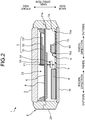
- FIG. 2 is a sectional view of the radio wave watch according to the embodiment
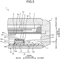
- FIG. 3 is a sectional view of a main part of the radio wave watch according to the embodiment
- FIG. 4 is a perspective view of an antenna according to the embodiment
- FIG. 5 is an illustrative view of an image antenna.
- a section II-II in FIG. 1 is illustrated in FIG. 2 .
- a radio wave watch 1 of the embodiment has an exterior case 2, a windshield 3, a dial plate 4, a hand 5, a solar cell 6, a substrate 7, a battery 8, an antenna 9, and a rear cover 10. Note that the illustration of the windshield 3, the dial plate 4, the hand 5, and the solar cell 6 is omitted in FIG. 1 .
- the radio wave watch 1 receives a radio wave from a satellite.
- the radio wave watch 1 has a function to correct its internal time based on information acquired from the radio wave.
- the radio wave watch 1 of the present embodiment receives a global positioning system (GPS) radio wave output from a GPS satellite.
- GPS global positioning system
- the GPS radio wave is a radio wave including GPS time information and uses, for example, two types of a 1.5 GHz band (1575.42 MHz) and a 1.2 GHz band (1227.60 MHz).
- the exterior case 2 is a member constituting the shell of the radio wave watch 1.
- the exterior case 2 is formed of a conductive material, such as titanium and titanium alloys.
- the exterior case 2 has an approximately cylindrical body part 21 and a lug 22.
- the body part 21 is a cylindrical constituent part where both ends in an axial direction are opened.
- the lug 22 is formed integrally with the body part 21 and projects from the circumferential surface of the body part 21 toward the outside in a radial direction.
- a belt is coupled to the lug 22.
- the direction of a center axis line X1 of the body part 21 is referred to as an "axial direction".
- the axial direction corresponds to a vertical direction of the radio wave watch 1.
- a direction perpendicular to the center axis line X1 is referred to as a "radial direction”
- a circumferential direction centered at the center axis line X1 is referred to as a "circumferential direction”.
- a side near the center axis line X1 is referred to as the "inside”
- a side far from the center axis line X1 is referred to as the "outside”.
- the windshield 3 blocks an opening on the front side of the body part 21.
- the windshield 3 is formed of a transparent material, such as glass.
- the windshield 3 covers the dial plate 4 and the hand 5 on the front side.
- the rear cover 10 blocks an opening on the back side of the body part 21.
- the rear cover 10 is a plate-shaped member and, for example, is formed of metal.
- the rear cover 10 covers the substrate 7 on the back side.
- the exterior case 2 has an accommodating space 23, the sectional shape of which is generally circular.
- the accommodating space 23 is an inner space of the body part 21.
- the accommodating space 23 is a closed space surrounded by the body part 21, the windshield 3, and the rear cover 10.
- the accommodating space 23 accommodates the dial plate 4, the hand 5, the solar cell 6, the substrate 7, the battery 8, and the antenna 9.
- the dial plate 4 is a disk-shaped member and fixed to the body part 21.
- the dial plate 4 is configured so that the dial plate 4 can pass light from the front side to the back side.
- the dial plate 4 is formed of an optically transparent material.
- the dial plate 4 may be formed of a non-conductive material, such as a synthetic resin.
- the hand 5 has a second hand 51, a minute hand 52, and an hour hand 53.
- the hand 5 is disposed coaxially with the center axis line X1 of the exterior case 2.
- a rotation shaft 55 of the hand 5 is passed through a through hole of the dial plate 4.
- Each of the second hand 51, the minute hand 52, and the hour hand 53 is coupled to a drive source, such as a motor, through a wheel train 54.
- the wheel train 54 is disposed on the back side relative to the dial plate 4 and decelerates the rotation of a drive source 56 to convey it to the hand 5.
- the drive source 56 of the present embodiment is a step motor.
- the drive source 56 rotationally drives the hand 5 with power supplied from the battery 8.
- the solar cell 6 is disposed on the back surface of the dial plate 4.
- the solar cell 6 is formed into a plane shape.
- the solar cell 6 converts received light into electric energy.
- the solar cell 6 is an aggregate of photovoltaic elements, and its front side is a light-receiving surface.
- the solar cell 6 generates electricity with light penetrating the dial plate 4.
- the solar cell 6 is electrically connected with the substrate 7.
- the power generated by the solar cell 6 may be supplied to devices of the radio wave watch 1, or may be charged into the battery 8.
- the substrate 7 is disposed in the vicinity of the rear cover 10 in the accommodating space 23.
- the substrate 7 is fixed to a main plate, which is not shown, and the main plate is fixed to the body part 21.
- the substrate 7 is disposed separately on the back side from the dial plate 4 in the axial direction and is opposed to the dial plate 4.
- the substrate 7 is a component of a controller controlling the radio wave watch 1.
- the substrate 7 has a control circuit 14 and a receiving circuit 15.
- the control circuit 14 controls driving of the drive source 56 and corrects the internal time.
- the receiving circuit 15 is connected with the antenna 9.
- the receiving circuit 15 decodes a satellite signal received by the antenna 9 to generate a digital signal.
- the digital signal generated by the receiving circuit 15 is sent to the control circuit 14.
- the control circuit 14 corrects the internal time based on the signal acquired from the receiving circuit 15.
- the control circuit 14 can correct display time of the hand 5 based on the internal time.
- the control circuit 14 has, in a storage region, geographic data where location information is associated with time zones and, from a result of the satellite reception, can determine a time zone to which a current location belongs to reflect it on the watch.
- a ground layer 70 is disposed on the substrate 7.
- the ground layer 70 may be formed of a ground plate formed of a conductive material, a ground electrode film formed on the substrate 7, or other components.
- the position and shape of the ground layer 70 is determined depending on the position and shape of the antenna 9.
- the ground layer 70 of the present embodiment is disposed to be opposed to the antenna 9 and an image antenna 9i (see FIG. 5 ).
- the ground layer 70 of the present embodiment is formed on a front surface 7a of the substrate 7.
- the ground layer 70 is electrically connected with the exterior case 2.
- the electrical connection may be either direct-current connection or alternate-current connection.
- the ground layer 70 may be connected with the exterior case 2 via an inner layer of the substrate 7. Note that the ground layer 70 may be electrically connected with the rear cover 10 instead of the exterior case 2.
- the shape of the ground layer 70 of the present embodiment is rectangular.
- the ground layer 70 has a first side 70a, a second side 70b, a third side 70c, and a fourth side 70d.
- the first side 70a is a side facing an inner wall surface 21a of the exterior case 2.
- the first side 70a and the fourth side 70d are opposed to each other in the radial direction.
- the second side 70b and the third side 70c are opposed to each other in the circumferential direction.
- the ground layer 70 is disposed so that a foot of a perpendicular line 70p drawn from the center axis line X1 to the first side 70a is the center of the first side 70a or a position in the vicinity of the center.
- each of the second side 70b and the third side 70c of the ground layer 70 is parallel to the perpendicular line.
- the first side 70a is a short side
- the second side 70b and the third side 70c are long sides.
- the first side 70a is slightly shorter than the second side 70b and the third side 70c. Note that the length of the first side 70a may be equal to the length of the second side 70b and the third side 70c.
- a width WG of the ground layer 70 is greater than a width WE of an emitting electrode 91 described below.
- the width WG of the ground layer 70 is greater than the width WE of the emitting electrode 91 and is smaller than the width WB of a base part 94.
- a width WS of a short-circuit part 92 (see FIG. 4 ) is equal to the width WE of the emitting electrode 91.
- the width WG of the ground layer 70 is thus greater than the width WS of the short-circuit part 92.
- the width WG of the ground layer 70 may be equal to the width WS of the short-circuit part 92.
- the fourth side 70d of the ground layer 70 is located at an inside end part in the radial direction of the antenna 9. More specifically, the fourth side 70d is located inside in the radial direction relative to the inside end part in the radial direction of the emitting electrode 91.
- the short-circuit part 92 is disposed between the first side 70a and the fourth side 70d of the ground layer 70.
- the emitting electrode 91 is disposed between the short-circuit part 92 and the fourth side 70d on the ground layer 70.
- the emitting electrode 91 is disposed between the second side 70b and the third side 70c of the ground layer 70.
- the fourth side 70d may be located inside relative to the inside end part in the radial direction of the antenna 9.
- the antenna 9 is disposed on the substrate 7. More specifically, the antenna 9 is disposed on the front surface 7a of the substrate 7. The antenna 9 is disposed between the center axis line X1 and the inner wall surface 21a of the exterior case 2.
- the antenna 9 has the emitting electrode 91, the short-circuit part 92, a connecting part 93, and the base part 94.
- the base part 94 is formed, of a dielectric, into a cubic shape.
- the base part 94 is formed of a non-conductive dielectric, such as a ceramic.
- the base part 94 is configured with a material having a high dielectric constant, such as zirconia or titanium oxide, and exhibits a wavelength-shortening effect.
- the shape of the base part 94 of the present embodiment is a rectangular parallelepiped.
- the base part 94 enables a substantial wavelength ⁇ ' of a radio wave that the emitting electrode 91 receives to be smaller than a wavelength ⁇ corresponding to the frequency of the GPS radio wave.
- the base part 94 is disposed so that a front surface 94a faces the front side, or the front surface 94a is opposed to the windshield 3.
- the base part 94 is disposed so that a first side surface 94c is opposed to the inner wall surface 21a of the exterior case 2 and a second side surface 94d faces the center axis line X1 side.
- the first side surface 94c and the second side surface 94d are side surfaces located across the front surface 94a and face in mutually opposite directions.
- the base part 94 of the present embodiment is disposed so that the position of a foot of a perpendicular line 94e drawn from the center axis line X1 to the second side surface 94d is the center position in a width direction of the second side surface 94d.
- the shape of the antenna 9 is symmetric with reference to the perpendicular line drawn from the center axis line X1 to the foot of the perpendicular line 94e.
- the first side surface 94c and the second side surface 94d of the present embodiment are side surfaces along the long side of the front surface 94a.
- the ground layer 70 is formed so that the fourth side 70d (see FIG. 3 ) is parallel to the second side surface 94d of the base part 94 and the first side 70a is parallel to the first side surface 94c of the base part 94.
- the base part 94 is disposed in an inside region in the radial direction of the ground layer 70.
- the emitting electrode 91 is disposed on the front surface 94a of the base part 94.
- the emitting electrode 91 is a planar constituent part formed of a material having conductivity, such as metal.
- the emitting electrode 91, as well as the short-circuit part 92 and the connecting part 93 described below may be configured with a conductive-material thin film formed on the dielectric, which is the base part 94, or may be configured with a plate-shaped member.
- the antenna 9 illustrated in the present embodiment is the one where a thin film is formed on the dielectric, but, instead of this, the antenna 9 may be configured only with a conductive plate-shaped member, or may be configured by combining the base part 94 with the conductive plate-shaped member.
- planar emitting electrode 91 examples include both the one configured with a thin film and the one formed into a plate shape.
- planar short-circuit part 92 and the connecting part 93 examples include both the ones configured with a thin film and the ones formed into a plate shape.
- planar emitting electrode 91, the short-circuit part 92, and the connecting part 93 also includes a configuration where they have an uneven part on the whole or part of their surfaces.
- the shape of the emitting electrode 91 of the present embodiment is rectangular.
- the emitting electrode 91 is disposed, on the front surface 94a, to cover a most region of the front surface 94a.
- the emitting electrode 91 is disposed to expose an edge part of the front surface 94a in a U shape. More specifically, a partial region inside in the radial direction of the front surface 94a and regions at both ends in the width direction thereof are exposed.
- Each side of the emitting electrode 91 is parallel to the corresponding side of the front surface 94a. Note that the emitting electrode 91 may be provided to prevent the exposure of the front surface 94a, in other words, cover the whole of the front surface 94a.
- the "width direction” is a direction perpendicular to an extension direction of the emitting electrode 91.
- the emitting electrode 91 of the present embodiment extends from the short-circuit part 92 along the radial direction.
- the "extension direction” in this case is a direction of the perpendicular line that links the center axis line X1 to the line of the perpendicular line 70p.
- the width direction is a direction perpendicular to this perpendicular line, and, for example, a direction parallel to the first side 70a of the ground layer 70.
- the emitting electrode 91 has first emitting sides 91a and 91a, and a second emitting side 91b.
- the first emitting sides 91a are sides along the radial direction of the emitting electrode 91.
- One of the first emitting sides 91a and the other of the first emitting sides 91a are generally parallel or substantially parallel.
- the second emitting side 91b is a side substantially perpendicular to the first emitting sides 91a of the emitting electrode 91, in other words, a side along the width direction.
- the substantial antenna length of the emitting electrode 91 is the length of a side from a point 91c, to which the short-circuit part 92 is connected, to the second emitting side 91b, i.e., the length of the first emitting sides 91a and 91a.
- the emitting electrode 91 is formed so that, for example, the antenna length is a length of 1/4 of the substantial wavelength ⁇ ' after shortening.
- the antenna 9 of the present embodiment has characteristics of a planar monopole antenna. More specifically, in the antenna 9 of the present embodiment, each of the first emitting sides 91a and 91a exhibits antenna characteristics similar to a monopole antenna.
- the first emitting sides 91a and 91a have directivity along the direction of the center axis line X1. That is to say, the first emitting sides 91a and 91a have high sensitivity to a radio wave along the direction of the center axis line X1.
- the short-circuit part 92 is disposed on the first side surface 94c of the base part 94.
- the first side surface 94c is a surface facing outside in the radial direction of the base part 94.
- the short-circuit part 92 is a planar constituent part formed of a material having conductivity, such as metal.
- the shape of the short-circuit part 92 is rectangular.
- the short-circuit part 92 extends from the upper end of the first side surface 94c to the lower end thereof.
- the short-circuit part 92 is disposed to expose both end parts in the width direction of the first side surface 94c.
- the upper end of the short-circuit part 92 leads to the emitting electrode 91 and is electrically connected with the emitting electrode 91.
- the lower end of the short-circuit part 92 is electrically connected with the ground layer 70.
- the width WS of the short-circuit part 92 is equal to the width WE of the emitting electrode 91.
- the connecting part 93 is disposed on the second side surface 94d of the base part 94.
- the second side surface 94d is a surface facing inside in the radial direction of the base part 94.
- the connecting part 93 is a planar constituent part formed of a material having conductivity, such as metal.
- the shape of the connecting part 93 is rectangular.
- the connecting part 93 extends from an end part on a back surface 94b side of the second side surface 94d to a position relatively on the front side as compared with the center.
- the connecting part 93 is an RF connecting part and connected to the receiving circuit 15. In the antenna 9 of the present embodiment, the connecting part 93 is capacitively coupled to the emitting electrode 91.
- the connecting part 93 and the emitting electrode 91 are separated without physical contact.
- the capacitive coupling of the connecting part 93 and the emitting electrode 91 achieves non-contact-type signal transmission. Impedance matching is achieved based on the distance between an end part on the front side of the connecting part 93 and the second emitting side 91b. Note that power may be supplied by directly connecting the connecting part 93 with the emitting electrode 91.
- the base part 94 is supported by the substrate 7 so that its back surface 94b contacts with the ground layer 70.
- the back surface 94b is opposed to an inside region in the radial direction of the ground layer 70.
- the first side surface 94c of the base part 94 is parallel to the first side 70a of the ground layer 70
- the second side surface 94d of the base part 94 is parallel to the fourth side 70d of the ground layer 70.
- the connecting part 93 and a connected electrode 75 are disposed at a predetermined distance to the ground layer 70.
- the connecting part 93 is connected to the receiving circuit 15 via the electrode 75.
- the electrode 75 it is preferable for the electrode 75 to be made as small as possible in terms of reducing influence on the impedance of the antenna 9. Furthermore, it is preferable for the distance between the electrode 75 and the ground layer 70 to be separated as far as possible. Furthermore, it is preferable for the electrode 75 and the ground layer 70 not to overlap in a planar manner.
- the ground layer 70 of the present embodiment has a first region 71 and a second region 72.
- the first region 71 is an inside region in the radial direction relative to the short-circuit part 92.
- the second region 72 is an outside region in the radial direction relative to the short-circuit part 92.
- the first region 71 and the second region 72 are continuous and constitute the single ground layer 70.
- the shape of the first region 71 and the shape of the second region 72 are the same. That is to say, the ground layer 70 has a symmetric shape with reference to the short-circuit part 92.
- a length LG1 of the first region 71 in the radial direction is equal to a length LG2 of the second region 72 in the radial direction.
- the width of the first region 71 and the width of the second region 72 are the same.
- the area of the first region 71 is equal to the area of the second region 72.
- the radio wave watch 1 of the present embodiment enables the reception sensitivity of the antenna 9 to be improved with the image antenna 9i.
- the image antenna 9i is a virtual antenna and paired with the antenna 9. It is thought that the image antenna 9i is generated on the opposite side to the emitting electrode 91 side across the short-circuit part 92.
- the image antenna 9i is generated in a shape symmetric to the antenna 9 and at a position symmetric to it with reference to the short-circuit part 92.
- the image antenna 9i includes a virtual electrode 91i.
- the virtual electrode 91i is a virtual constituent part formed, by an image effect, at the position symmetric to the emitting electrode 91 with reference to the short-circuit part 92.
- the virtual electrode 91i extends from the short-circuit part 92 toward the outside in the radial direction and is opposed to the second region 72 of the ground layer 70.
- the radio wave watch 1 of the present embodiment enables the reception sensitivity of the antenna 9 to be improved to the maximum.
- a mounted object may be disposed in the region where the image antenna 9i is generated. Disposing the mounted object in the region for generating the image antenna 9i enables a power-supplying line to the mounted object to be shortened, and can decrease the influence of wiring capacity and reducing propagation loss.
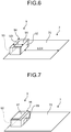
- FIGS. 6 and 7 One example of a placement of the antenna 9 on the ground layer 70 is illustrated in FIGS. 6 and 7 .
- Each antenna 9 in FIGS. 6 and 7 is disposed at an end part of the ground layer 70, and the positions of their short-circuit part 92 are different.
- the short-circuit part 92 faces the central side of the ground layer 70, similarly to the placement of the radio wave watch 1 of the present embodiment.
- the ground layer 70 extends frontward from the short-circuit part 92, in the placement of the antenna 9 in FIG. 6 .
- a length LGX of the ground layer 70 extending forward from the short-circuit part 92 is twice or more than a length LB of the base part 94.
- the short-circuit part 92 of the antenna 9 illustrated in FIG. 7 faces the opposite side to the central side of the ground layer 70. In this case, no ground layer 70 substantially exists forward from the short-circuit part 92. That is, FIGS. 6 and FIG. 7 have the difference of whether the ground layer 70 is provided forward from the short-circuit part 92.
- the placement of the antenna 9 in FIG. 6 is referred to as a "first placement”
- the placement of the antenna 9 in FIG. 7 is referred to as a "second placement”.
- FIG. 8 illustrates the sensitivity of the antenna 9 in the first placement and the second placement.
- the vertical axis represents the reception sensitivity C/N [dB] of the antenna 9.
- FIG. 8 illustrates the sensitivity to a radio wave received from four GPS satellites.
- the reception sensitivity in the first placement is better than the reception sensitivity in the second placement. That is, it is found that the reception sensitivity of the antenna 9 in the case where the ground layer 70 exists forward from the short-circuit part 92 is improved as compared with the case where no ground layer 70 exists. It is considered that this is because the ground layer 70 forward from the short-circuit part 92 results in forming the image antenna 9i having high symmetricity to the antenna 9.
- FIG. 9 is a view illustrating a configuration where the ground layer is extended in the first placement
- FIG. 10 is a perspective view illustrating a configuration where the ground layer is extended in the second placement.
- the ground layer 70 illustrated in FIGS. 9 and 10 has an extension part 70X.
- the extension part 70X is a part where the end part of the ground layer 70, on the side where the antenna 9 is disposed, is extended.
- the extension part 70X in the first placement extends frontward from the connecting part 93.
- the part, of the ground layer 70, disposed forward from the short-circuit part 92 has no change from that in FIG. 6 .
- extension part 70X in the second placement extends forward from the short-circuit part 92, as illustrated in FIG. 10 . That is, the ground layer 70 is added forward from the short-circuit part 92 as compared with the configuration in FIG. 7 .
- the length LX of the extension part 70X is similar to the length LB of the base part 94.
- FIG. 11 illustrates a measurement result of the reception sensitivity in the first placement.
- FIG. 12 illustrates a measurement result of the reception sensitivity in the second placement.
- FIG. 11 illustrates, in the first placement, the reception sensitivity in the case where no extension part 70X is provided ( FIG. 6 ) and the reception sensitivity in the case where the extension part 70X is provided ( FIG. 9 ).
- FIG. 12 illustrates, in the second placement, the reception sensitivity in the case where no extension part 70X is provided ( FIG. 7 ) and the reception sensitivity in the case where the extension part 70X is provided ( FIG. 10 ).
- the presence or absence of the extension part 70X in the first placement has no large influence on the reception sensitivity of the antenna 9.
- the presence or absence of the extension part 70X in the second placement have significant influence on the reception sensitivity of the antenna 9.
- the reception sensitivity is significantly improved as compared with the case where no extension part 70X is provided.
- FIG. 13 illustrates a configuration where a metal cover 12 is put on in the first placement.
- FIG. 14 illustrates a configuration where the metal cover 12 is put on in the second placement.
- the cover 12 is a box-shaped member configured with metal having conductivity.
- the cover 12 covers the surroundings of the ground layer 70 and the antenna 9.
- the cover 12 is electrically connected with the ground layer 70.
- a height HC of the cover 12 is approximately twice the length LB of the base part 94.
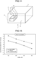
- FIG. 15 illustrates a measurement result of the reception sensitivity in the first placement.
- FIG. 16 illustrates a measurement result of the reception sensitivity in the second placement.
- FIG. 15 illustrates, in the first placement, the reception sensitivity in the case where no cover 12 is provided ( FIG. 6 ) and the reception sensitivity in the case where the cover 12 is provided ( FIG. 13 ).
- FIG. 16 illustrates, in the second placement, the reception sensitivity in the case where no cover 12 is provided ( FIG. 7 ) and the reception sensitivity in the case where the cover 12 is provided ( FIG. 14 ).
- the presence or absence of the cover 12 in the first placement have significant influence on the reception sensitivity of the antenna 9.
- the reception sensitivity significantly drops as compared with the case where no cover 12 is provided.
- the presence or absence of the cover 12 in the second placement has influence on the reception sensitivity to some extent.
- the reception sensitivity also drops as compared with the case where no cover 12 is provided.
- the degree of drop in the reception sensitivity in the second placement is smaller than the degree of drop in the reception sensitivity in the first placement. That is, it is said that the second placement has high tolerance to the metal enclosure as compared with the first placement.
- the connecting part 93 which is capacitively coupled to the emitting electrode 91, is disposed near the cover 12, which is the metal member, and thus the reception sensitivity drops under the influence of the metal of the cover 12.
- each component is disposed so that the metal member does not cover the antenna 9 and the image antenna 9i from above.
- the solar cell 6 is disposed not to cover the second region 72 of the ground layer 70 and the antenna 9 from above. More specifically, an end surface 6a of the solar cell 6 is located inside in the radial direction relative to the emitting electrode 91. That is, the solar cell 6 is disposed not to overlap with at least the emitting electrode 91 when viewed in the axial direction.
- the radio wave watch 1 of the present embodiment thus enables the reception sensitivity of the antenna 9 to be improved.
- FIG. 17 is a plan view illustrating a placement example of the solar cell.
- the shape of the solar cell 6 illustrated in FIG. 17 is a shape where a part of its disk is notched.
- the solar cell 6 has a sector-shaped notch part 6b.
- the width of the notch part 6b becomes wider as it goes outside in the radial direction from the center axis line X1.
- the shape and placement of the notch part 6b are determined so that the solar cell 6 does not overlap with the antenna 9 and the ground layer 70 when viewed in the axial direction. That is, the notch part 6b is formed so that the solar cell 6 does not shield the front side of the antenna 9 and the ground layer 70.
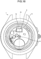
- FIG. 18 is a plan view illustrating a placement example of a date plate.
- the date plate 13 may overlap with the ground layer 70 when viewed in the axial direction.
- the date plate 13 is disposed coaxially with the center axis line X1.
- the date plate 13 is disposed to overlap with the second region 72 of the ground layer 70 and not to overlap with the antenna 9.
- the date plate 13 is disposed outside in the radial direction relative to the antenna 9.
- the non-conductive member is unlikely to affect the symmetricity between the antenna 9 and the image antenna 9i even when it is disposed at a position opposed to the ground layer 70.
- FIG. 19 is a plan view illustrating another placement example of the antenna.
- the short-circuit part 92 of the antenna 9 is disposed to face in the circumferential direction.
- the emitting electrode 91 extends from the short-circuit part 92 along the circumferential direction, in the placement illustrated in FIG. 19 .
- the second region 72 of the ground layer 70 extends from the antenna 9 toward the opposite side to the emitting electrode 91 side along the circumferential direction.
- the antenna 9 is disposed so that the short-circuit part 92 is located on a virtual plane S1.
- the virtual plane S1 is a plane including the center axis line X1.
- the antenna 9 is disposed so that the short-circuit part 92 extends along the virtual plane S1 in the radial direction.
- the ground layer 70 is disposed to be symmetric with reference to the virtual plane S1. That is, in the ground layer 70, the first region 71 and the second region 72 are located on the different sides across the virtual plane S1.
- the placement as illustrated in FIG. 19 also enables the reception sensitivity of the antenna 9 to be improved by the effect of the image antenna 9i.
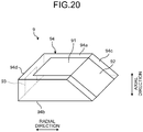
- FIG. 20 is a perspective view illustrating one example of the shape of the antenna.
- the first side surface 94c of the base part 94 is an inclined surface.
- the first side surface 94c is inclined to approach the second side surface 94d as it goes from the back surface 94b side to the front surface 94a side.
- the short-circuit part 92 is inclined similarly to the first side surface 94c.
- Various shapes other than the illustrated one can be adopted as the shape of the antenna 9.
- the radio wave watch 1 has the exterior case 2, the dial plate 4, the substrate 7, the first region 71 of the ground layer 70, the antenna 9, and the second region 72 of the ground layer 70.
- the dial plate 4 is disposed within the exterior case 2.
- the first region 71 of the ground layer 70 corresponds to a first ground layer disposed on the substrate 7.
- the antenna 9 is disposed between the center axis line X1, which is the center of the exterior case 2, and the inner wall surface 21a of the exterior case 2.
- the antenna 9 has the planar emitting electrode 91, the planar short-circuit part 92, and the connecting part 93.
- the emitting electrode 91 is opposed to the first region 71 of the ground layer 70.
- the short-circuit part 92 electrically connects the end part of the emitting electrode 91 with the first region 71 of the ground layer 70.
- the connecting part 93 connects the emitting electrode 91 with the receiving circuit 15 of the substrate 7.
- the second region 72 of the ground layer 70 corresponds to a second ground layer disposed on the substrate 7.
- the second region 72 is disposed on the opposite side to the emitting electrode 91 side across the short-circuit part 92 on the substrate 7.
- the width WG of the second region 72 is equal to or greater than the width WS of the short-circuit part 92.
- the first region 71 as the first ground layer and the second region 72 as the second ground layer are integrated with each other.
- the integration of the first region 71 and the second region 72 facilitates improving the symmetricity between the image antenna 9i and the antenna 9.
- the configuration of the ground layer 70 is simplified.
- the emitting electrode 91 extends from the short-circuit part 92 toward the radial direction, which is a direction perpendicular to the center axis line X1 of the exterior case 2. Such a placement easily secures the symmetricity of the emitting electrode 91 in positional relationship with the inner wall surface 21a of the exterior case 2.
- the second region 72 of the ground layer 70 extends from the short-circuit part 92 toward the opposite side to the emitting electrode 91 side.
- the length LG2 of the second region 72 in this extension direction is equal to or greater than a length LE of the emitting electrode 91.
- the second region 72 of the present embodiment can improve the symmetricity between the image antenna 9i and the antenna 9.
- the length LG2 of the second region 72 may be less than the length LE of the emitting electrode 91.
- the length LG2 of the second region 72 is determined depending on the size of a region to be secured.
- the shape of the first side 70a may be an arc shape corresponding to the shape of the inner wall surface 21a of the exterior case 2, instead of the straight shape. This enables a limited space to be effectively utilized to enhance the symmetricity between the first region 71 and the second region 72.
- the metal member is disposed in a region not overlapping with the emitting electrode 91 in the direction of the center axis line X1 of the exterior case 2, in the space between the dial plate 4 and the substrate 7.
- the solar cell 6 is disposed in the region not overlapping with the emitting electrode 91 when viewed in the axial direction, as illustrated in FIG. 17 .
- the drive source 56 and the wheel train 54 are also disposed in the region not overlapping with the emitting electrode 91 when viewed in the axial direction. Disposing the metal member in the region not overlapping with the emitting electrode 91 enables the reception sensitivity of the antenna 9 to be improved.
- the metal member may be disposed in a region overlapping with the second region 72.
- the metal member disposed in the region overlapping with the second region 72 is, for example, the solar cell 6, the drive source 56, a magnetic shield, and the wheel train 54.
- FIG. 21 illustrates the solar cell 6 disposed to overlap with the second region 72.
- the solar cell 6 is opposed to the second region 72 of the ground layer 70 in the axial direction.
- the solar cell 6 has an opening part 6c at a position opposed to the emitting electrode 91.
- the shape of the opening part 6c is rectangular.
- the opening part 6c is provided in a range overlapping with the emitting electrode 91 when viewed in the axial direction.
- the opening width and the opening length of the opening part 6c may be greater than the width WE and the length LE of the emitting electrode 91, respectively. Disposing the solar cell 6 also in the region overlapping with the second region 72 can achieve maximizing the light-receiving area of the solar cell 6 while achieving improvement in the reception sensitivity of the antenna 9.
- the solar cell 6 overlaps with the whole region of the second region 72, but it is not limited to this.
- the solar cell 6 may overlap with a partial region of the second region 72.
- the region overlapping with the second region 72 may have an opening, a slit, or other empty spaces.
- a part of the opening part 6c may be formed to overlap with the second region 72 when viewed in the axial direction.
- the solar cell 6 of the antenna 9 may have the notch part 6b as illustrated in FIG. 17 .
- the solar cell 6 illustrated in FIG. 17 has the notch part 6b at a position opposed to the emitting electrode 91 and the second region 72.
- the notch part 6b includes a range overlapping with the emitting electrode 91 and the second region 72 when viewed in the axial direction. The solar cell 6 does not shield the front side of the emitting electrode 91 and the second region 72, so that the drop in the reception sensitivity of the antenna 9 is reduced.
- a non-conductive member may be disposed to be opposed to the second region 72.
- the wheel train 54 is a non-conductive member
- the wheel train 54 may be disposed to be opposed to the second region 72.
- the non-conductive member is disposed to be opposed to the second region 72 in this way, so that the space between the second region 72 and the dial plate 4 is effectively utilized.
- the non-conductive member unlikely affects the characteristics of the image antenna 9i. This enables the limited space within the exterior case 2 to be effectively utilized while achieving improvement in the reception sensitivity of the antenna 9.
- the radio wave watch 1 may have a planar, non-conductive rotating member opposed to the substrate 7, for example, the date plate and a day plate.
- this rotating member it is preferable for this rotating member to be disposed not to overlap with the emitting electrode 91 and disposed to overlap with the second region 72, in the direction of the center axis line X1 of the exterior case 2.
- the date plate 13 illustrated in FIG. 18 is disposed in the outermost periphery in the inner space of the exterior case 2.
- the inner periphery of the date plate 13 is located, at least, outside in the radial direction relative to the emitting electrode 91.
- a part of the date plate 13 overlaps with the second region 72 of the ground layer 70 when viewed in the axial direction.
- Such a placement can achieve enlarging the date plate 13 in diameter while reducing the influence on the reception sensitivity of the antenna 9.
- the connecting part 93 of the present embodiment connects the emitting electrode 91 with the receiving circuit 15 by capacitive coupling.
- the connecting part 93 is disposed at a position that is closer to the center of the exterior case 2 than the short-circuit part 92 is.
- the connecting part 93 is far from the inner wall surface 21a of the exterior case 2, so that the capacitive coupling between the connecting part 93 and the emitting electrode 91 is unlike to be affected by the exterior case 2.
- the antenna center of the antenna 9 is disposed on the straight line that links the center of the battery 8 to the center axis line X1, but this placement is one example.
- the center of the antenna 9 is disposed at the position of approximately 12 o'clock, and the center of the battery 8 is disposed at the position of approximately 6 o'clock.
- the center of the antenna 9 may be disposed at a position between 9 o'clock and 11 o'clock, and the center of the battery 8 may be disposed at a position between 4 o'clock and 6 o'clock.
- the shape of the first region 71 may be different from the shape of the second region 72.
- the length LG1 of the first region 71 may be different from the length LG2 of the second region 72.
- the length LG1 of the first region 71 may be greater than the length LG2 of the second region 72.
- the antenna 9 receives the radio wave, but also it may be used for transmitting the radio wave.
- the antenna 9 may be used to perform transmission to and reception from peripheral equipment.
- the electronic watch 1 may communicate with other equipment via short-distance wireless communication by, for example, Bluetooth (registered trademark) or Wi-Fi.
- the antenna 9 transmits the radio wave
- power is supplied to the emitting electrode 91 through the connecting part 93.
- the radio wave watch 1 may have a radio communication circuit including the receiving circuit 15 and a transmitting circuit.
- the connecting part 93 connects the radio communication circuit with the emitting electrode 91.
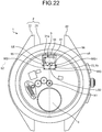
- FIG. 22 is a plan view illustrating a radio wave watch according to the first variation of the embodiment
- FIG. 23 is a perspective view of an antenna according to the first variation of the embodiment
- FIG. 24 is a front view of the antenna according to the first variation of the embodiment
- FIG. 25 is a side view describing the directivity of the antenna.
- the antenna 9 of the first variation has a connecting part 96 instead of the connecting part 93 of the above embodiment.
- the configuration other than the antenna 9 is similar to that of the above embodiment.
- the connecting part 96 connects the receiving circuit 15 to the emitting electrode 91 physically and electrically.
- the connecting part 96 is a planar constituent part and disposed on the first side surface 94c.
- the connecting part 93 of the above embodiment indirectly connects the emitting electrode 91 to the receiving circuit 15 by capacitive coupling.
- the connecting part 96 of the first variation directly connects the emitting electrode 91 to the receiving circuit 15.
- the first side surface 94c faces inside in the radial direction.
- the antenna 9 of the first variation has a paired short-circuit parts 95 and 95.
- Each of the paired short-circuit parts 95 and 95 is a planar constituent part and disposed on the first side surface 94c.
- the paired short-circuit parts 95 and 95 are disposed in line with the connecting part 96 on both sides of the connecting part 96.
- the paired short-circuit parts 95 and 95 each extend along the axial direction and are disposed apart from each other in the width direction.
- the connecting part 96 is disposed between the paired short-circuit parts 95 and 95 and extends along in the axial direction.
- the connecting part 96 and the paired short-circuit parts 95 and 95 extend along a virtual plane S2.
- the virtual plane S2 is a plane parallel to the center axis line X1 of the exterior case 2. That is, the connecting part 96 and the paired short-circuit parts 95 and 95 extend to be perpendicular to a perpendicular line drawn from the center axis line X1 to the virtual plane S2.
- the connecting part 96, and the paired short-circuit parts 95 and 95 are connected mutually at an end part of the emitting electrode 91 side. That is, the connecting part 96, and the paired short-circuit parts 95 and 95 constitute one conductive member.
- the direction of a current Ia flowing through the connecting part 96 and the direction of a current Ib flowing through the short-circuit part 95 are opposite to each other.
- a substantial power-supplying point is a power-supplying part 97 illustrated in FIG. 24 .
- the direction of the current Ia and the direction of the current Ib are opposite to each other and cancelled mutually, so that the connecting part 96 fails to contribute to substantial emission. That is, the connecting part 96 functions as a transmission path that fails to contribute to emission.
- the emitting electrode 91 of the antenna 9 mainly contributes to emission.
- the antenna 9 has its directivity along the axial direction as illustrated in FIG. 25 . That is, the antenna 9 can receive a radio wave traveling along the axial direction with high sensitivity.
- each of the paired short-circuit parts 95 and 95 has a width WS1.
- the paired short-circuit parts 95 and 95 are formed into the same shape.
- the width WS1 of the short-circuit part 95 is greater than a width WP of the connecting part 96.
- the antenna 9 is disposed so that the short-circuit part 95 and the connecting part 96 face inside in the radial direction.
- the emitting electrode 91 extends from the connecting part 96 toward the outside in the radial direction. In other words, the emitting electrode 91 extends from the connecting part 96 toward the inner wall surface 21a of the exterior case 2 along the radial direction.
- the second region 72 of the ground layer 70 is disposed inside in the radial direction relative to the antenna 9. Also in the first variation, the position of the second region 72 is the opposite position to the emitting electrode 91 side across the short-circuit part 95 on the substrate 7.
- the width WG of the second region 72 is equal to or greater than the width WS1 of the short-circuit part 95.
- the ground layer 70 has the first region 71 corresponding to the antenna 9.
- the shape of the first region 71 may be the same as that of the second region 72. It is preferable for the length LG2 of the second region 72 to be equal to or greater than the length LE of the emitting electrode 91.
- the inside in the radial direction relative to the antenna 9 is the region of the image antenna 9i.
- the second region 72 of the ground layer 70 enhances the symmetricity between the antenna 9 and the image antenna 9i. This improves the reception sensitivity of the antenna 9 also in the radio wave watch 1 of the first variation.
- the shape of the antenna 9 may be a shape as illustrated in FIG. 26 .
- the first side surface 94c of the base part 94 is an inclined face.
- the first side surface 94c is inclined to approach the second side surface 94d as it goes from the back surface 94b side to the front surface 94a side.
- the short-circuit parts 95 and 95 and the connecting part 96 are inclined similarly to the first side surface 94c.
- the emitting electrode 91 may extend to a surface other than the front surface 94a of the base part 94.
- the emitting electrode 91 may extend from the front surface 94a to the second side surface 94d.
- the extension of the emitting electrode 91 over a plurality of surfaces can achieves downsizing the antenna 9.
- Various shapes other than the illustrated one can be adopted as the shape of the antenna 9.
- the metal member in the radio wave watch 1 of the first variation, it is preferable for the metal member to be disposed in the region not overlapping with the emitting electrode 91 in the direction of the center axis line X1.
- the metal member may be disposed in the region overlapping with the second region 72 of the ground layer 70.
- the solar cell 6 may have a notch part at the position opposed to the emitting electrode 91 and the second region 72.
- the non-conductive member may be disposed to be opposed to the second region 72 of the ground layer 70.
- this rotating member may be disposed not to overlap with the emitting electrode 91 and disposed to overlap with the second region 72, in the direction of the center axis line X1.
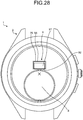
- FIG. 28 is a plan view of a radio wave watch according to the second variation of the embodiment.
- the battery 8 functions as the second ground layer.
- the battery 8 is disposed so that its negative electrode faces the front side.
- the antenna 9 is disposed adjacently to the battery 8 so that the short-circuit part 92 faces the battery 8.
- the battery 8 is thus located on the opposite side to the emitting electrode 91 across the short-circuit part 92.
- the negative electrode of the battery 8 functions as the second ground layer and enables the symmetricity between the antenna 9 and the image antenna 9i to be improved.
- the antenna 9 of the above embodiment may be disposed adjacently to the battery 8.
- the antenna 9 is disposed adjacently to the battery 8 so that the paired short-circuit parts 95 and 95 face the battery 8.
- the connecting part 96 of the antenna 9 may be disposed close to the exterior case 2 side, with the exterior case 2 set to the ground potential.
- the exterior case 2 also functions as the second region 72.
- such a placement is effective in the case where it is difficult to secure a space on the substrate 7 for the second region 72.
- FIG. 29 is a plan view of a radio wave watch according to the third variation of the embodiment.
- the antenna 9 of the third variation is disposed similarly to the antenna 9 of the above embodiment.
- the solar cell 6 of the third variation has a projecting part 6d, which overlaps with the antenna 9 when viewed in the axial-direction.
- the solar cell 6 is provided with the notch part 6b and has the projecting part 6d at the center in the circumferential direction of the notch part 6b.
- the projecting part 6d extends from the center axis line X1 toward the outside in the radial direction.
- the projecting part 6d is a rectangular constituent part having a constant width.
- the projecting part 6d is disposed to overlap with a central part in the width direction of the emitting electrode 91 and the ground layer 70.
- the width of the projecting part 6d is less than both the width WE of the emitting electrode 91 and the width WG of the ground layer 70. Thus, the projecting part 6d does not overlap with the first emitting sides 91a and 91a of the emitting electrode 91.
- the projecting part 6d overlaps with the central part of the second emitting side 91b when viewed in the axial-direction.
- the central part of the second emitting side 91b is a part where its potential fluctuation is smaller than that in the first emitting side 91a.
- the projecting part 6d can increase the light-receiving area of the solar cell 6 while reducing the influence on the reception sensitivity of the emitting electrode 91.
- FIG. 30 is a plan view of a radio wave watch according to the fourth variation of the embodiment.
- the antenna 9 of the fourth variation is curved along the shape of the inner wall surface 21a of the exterior case 2.
- each of the first side surface 94c and the second side surface 94d of the base part 94 is a curved surface having an arc shape.
- Each shape of the first side surface 94c and the second side surface 94d is an arc shape concentric with the inner wall surface 21a of the exterior case 2.
- the paired short-circuit parts 95 and 95 and the connecting part 96 are disposed along the first side surface 94c. That is, the paired short-circuit parts 95 and 95 and the connecting part 96 extend along a curved surface parallel to the center axis line X1.
- the shape of the emitting electrode 91 is a curved shape similar to the base part 94.
- the shape of the second emitting side 91b is an arc shape concentric with the inner wall surface 21a of the exterior case 2.
- the first emitting sides 91a are inclined to approach mutually as they go inside in the radial direction.
- the shape of the ground layer 70 is a curved shape similar to the base part 94.
- Each shape of the first side 70a and the fourth side 70d is an arc shape concentric with the inner wall surface 21a of the exterior case 2.
- the second side 70b and the third side 70c are inclined to approach mutually as they go inside in the radial direction. It is desirable that the curvature of the curved shape of the ground layer 70 be a curvature where a distance from the center axis line X1 is assumed as a radius.
- a rotating member e.g., a date plate
- the antenna 9 is disposed in the outside region in the radial direction of the ground layer 70. That is, the outside region in the radial direction of the ground layer 70 is the first region 71, and the inside region in the radial direction is the second region 72.
- the first emitting sides 91a of the emitting electrode 91 may be parallel to each other.
- the second side 70b and the third side 70c of the ground layer 70 may be parallel.
- the antenna 9 of the above embodiment i.e., the antenna 9 where power is supplied to the emitting electrode 91 by capacitive coupling may have a curved shape.
- the antenna 9 may be disposed in the inside region in the radial direction of the ground layer 70. It is preferable for the connecting part 93 to be disposed toward the inside in the radial direction.
- FIG. 31 is a sectional view of a radio wave watch according to the fifth variation of the embodiment.
- a first ground layer 73 and a second ground layer 74 are separated.
- the ground layer 70 has the first ground layer 73 and the second ground layer 74.
- the first ground layer 73 is disposed on the front surface 7a of the substrate 7.
- the second ground layer 74 is disposed within the substrate 7.
- the ground layer 70 is configured so that the potential of the first ground layer 73 is the same as that of the second ground layer 74.
- the first ground layer 73 and the second ground layer 74 may be electrically connected via a through hole formed in the substrate 7.
- the second ground layer 74 is disposed on the opposite side to the first ground layer 73 across the short-circuit part 92.
- the first ground layer 73 is disposed inside in the radial direction relative to the second ground layer 74.
- the first ground layer 73 and the second ground layer 74 may be disposed in different layers in the substrate 7. This can contribute to downsizing and thinning because a mounted object 16 having a physical height and the antenna 9 can be disposed on the same plane.
- the first ground layer 73 and the second ground layer 74 may be disposed independently in the same layer of the substrate 7.
- the second ground layer 74 may be disposed on the back side (the rear cover 10 side) of the substrate 7.
- FIG. 32 is a sectional view of a main part of a radio wave watch according to the sixth variation of the embodiment. As illustrated in FIG. 32 , the antenna 9 is disposed to be embedded in the substrate 7.
- the ground layer 70 according to the sixth variation has a first ground layer 76 and a second ground layer 77.
- the substrate 7 according to the sixth variation is a stacked substrate.
- the first ground layer 76 is formed in the bottom layer.
- the bottom layer is the most back-side layer in a stacked direction of the substrate 7.
- the substrate 7 has a concave part 7b to expose the first ground layer 76.
- the antenna 9 is accommodated in the concave part 7b.
- the second ground layer 77 is formed on the front surface 7a of the substrate 7.
- the second ground layer 77 is disposed on the opposite side to the first ground layer 76 across the short-circuit part 92.
- the second ground layer 77 is disposed on the opposite side to the emitting electrode 91 across the short-circuit part 92.
- the first ground layer 76 and the second ground layer 77 are electrically connected.
- the configuration of this variation contributes to thinning of the watch, for example.
- the second ground layer 77 may be disposed in a middle layer or the bottom layer of the substrate 7, instead of the front surface 7a.
- FIG. 33 is a plan view of an antenna according to the seventh variation of the embodiment.
- the first emitting side 91a is formed into a meander shape.
- the first emitting side 91a has continuously formed unevenness. Making the first emitting side 91a into the meander shape enables the antenna 9 to be downsized while securing a required antenna length.
- the second emitting side 91b may be formed into a meander shape.
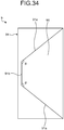
- FIG. 34 is a plan view of an antenna according to the eighth variation of the embodiment
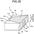
- FIG. 35 is a perspective view of the antenna according to the eighth variation of the embodiment
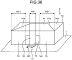
- FIG. 36 is a front view of the antenna according to the eighth variation of the embodiment
- FIG. 37 is a plan view illustrating a placement example of the antenna according to the eighth variation of the embodiment
- FIG. 38 is a plan view illustrating one example of the shape of the solar cell
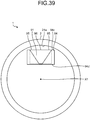
- FIG. 39 is a plan view illustrating another placement example of the antenna.
- an intersection angle of the second emitting side 91b and the first emitting side 91a is different from a right angle.
- the first emitting side 91a extends so that an intersection angle ⁇ with the second emitting side 91b is an obtuse angle.
- Such an extension of the first emitting side 91a in a slanting direction can lengthen the length of the first emitting side 91a as compared with the case where the intersection angle ⁇ is the right angle.
- the antenna 9 can be downsized while a required antenna length is secured.
- the shape of the emitting electrode 91 of the eighth variation is a tapering shape in which its width becomes narrower as it goes from the base end to the tip.
- the base end side of the emitting electrode 91 is a side where the short-circuit part 95 and the connecting part 96 are connected, i.e., the first side surface 94c side, and the tip side of the emitting electrode 91 is the second side surface 94d side.
- the area of the emitting electrode 91 is increased, for example.
- the base part 94 as a foundation is extended.
- the substantial wavelength ⁇ ' is shortened by the wavelength-shortening effect as the frame of the base part 94 becomes larger.
- the antenna 9 of the eighth variation can maximize the area of the emitting electrode 91 and the length of the first emitting side 91a without excessively increasing the frame of the base part 94.
- first emitting side 91a and the second emitting side 91b may be formed into a meander shape. In terms of obtaining stable characteristics of the antenna 9, it is desirable to secure the symmetricity between the inclined, paired first emitting sides 91a and 91a.
- the width WS1 (see FIG. 36 ) of the short-circuit part 95 is preferable for the width WS1 (see FIG. 36 ) of the short-circuit part 95 to be increased in a feasible range, and it is preferable for the width WP of the connecting part 96 to be decreased in a feasible range.
- the width WS1 of the short-circuit part 95 may be greater than the width WP of the connecting part 96.
- Increasing the width WS1 of the short-circuit part 95 enhances, for example, the effect of the sensitivity improvement by the image antenna 9i.
- Decreasing the width WP of the connecting part 96 can decrease a width WN of the electrode 75 of the substrate 7. Decreasing the width WN of the electrode 75 reduces capacitive coupling of the electrode 75 with another electrode of a circuit of the substrate 7 and other surrounding metal members. As a result, the impedance matching about the antenna 9 is facilitated.
- the antenna 9 of the eighth variation is disposed as illustrated in FIG. 37 .
- the antenna 9 in FIG. 37 is disposed so that the short-circuit part 95 and the connecting part 96 face inside in the radial direction. That is, the connecting part 96 is opposed to the center axis line X1 in the radial direction.
- the base part 94 may be disposed so that the second side surface 94d is close to the inner wall surface 21a.
- the base part 94 is disposed near the inner wall surface 21a, so that a space for placing other parts is easily secured in the vicinity of the center axis line X1. Furthermore, a space for the image antenna 9i is easily secured inside in the radial direction relative to the antenna 9.
- the solar cell 6 may have a shape as illustrated in FIG. 38 .
- the solar cell 6 has a notch part 60 at a position opposed to the antenna 9.
- the notch part 60 is formed not to overlap with at least the emitting electrode 91 in the axial direction.
- the notch part 60 has a first side 60a, second sides 60b and 60c, and inclined sides 60d and 60e.
- the first side 60a is a side parallel to the first side surface 94c of the base part 94.
- the first side 60a is located inside in the radial direction relative to the first side surface 94c.
- the second sides 60b and 60c are sides extending along end surfaces 94f and 94g of the base part 94.
- the second sides 60b and 60c are substantially parallel to the end surfaces 94f and 94g.
- the inclined sides 60d and 60e link the first side 60a to the second sides 60b and 60c.
- the inclined sides 60d and 60e extend in a direction inclined relative to the first side 60a and the second sides 60b and 60c.
- the inclined sides 60d and 60e extend along the radial direction from the center axis line X1.
- the second sides 60b and 60c are opposed to the first emitting side 91a of the emitting electrode 91.
- the second sides 60b and 60c extend in a direction intersecting with the first emitting side 91a. More specifically, in planar view, the second sides 60b and 60c are separated from the first emitting side 91a as they go outside in the radial direction.
- the second sides 60b and 60c extend in the direction intersecting with the first emitting side 91a, so that currents flowing the second sides 60b and 60c are unlikely to cause the drop in the sensitivity of the emitting electrode 91.
- the solar cell 6 of the eighth variation can achieve maximizing the solar cell 6 while reducing the drop in the sensitivity of the antenna 9.
- the antenna 9 may be disposed as illustrated in FIG. 39 .
- the antenna 9 illustrated in FIG. 39 is disposed so that the short-circuit part 95 and the connecting part 96 face outside in the radial direction. That is, the connecting part 96 is opposed to the inner wall surface 21a of the exterior case 2 in the radial direction. This placement can increase the distance between the first emitting side 91a of the emitting electrode 91 and the inner wall surface 21a.
- FIG. 40 is a plan view illustrating a placement of a motor according to the ninth variation of the embodiment.
- a part of a motor 11 is disposed at a position opposed to the short-circuit part 95 in the radial direction.
- the motor 11 is an electromagnetic motor, and has a housing 11a, a coil 11b, and a rotor 11c.
- the motor 11 rotates the rotor 11c with an induced electromotive force that is generated by powering the coil 11b.
- the motor 11 is installed in the electronic watch 1 as a drive source rotating the hand.
- the motor 11 is disposed so that the rotor 11c is located on the opposite side to the antenna 9 side relative to the coil 11b.
- the antenna 9 of the ninth variation is disposed so that the short-circuit part 95 faces inside in the radial direction.
- the motor 11 is disposed inside in the radial direction relative to the antenna 9.
- the motor 11 is disposed so that the rotor 11c is located inside in the radial direction relative to the coil 11b.
- the coil 11b thus extends between the rotor 11c and the antenna 9.
- the electronic watch 1 has a magnetic shield 17.
- the magnetic shield 17 covers the rotor 11c. That is, the magnetic shield 17 shields the rotor 11c in the axial direction.
- the magnetic shield 17 of this variation is disposed to cover the rotor 11c and not to cover the antenna 9.
- the rotor 11c of the motor 11 is disposed apart from the antenna 9, so that the magnetic shield 17 can be disposed at a position with few influence on the emitting electrode 91. As a result, the magnetic shield 17 is unlikely to cause the drop in the sensitivity of the antenna 9.
- the placement of the ninth variation achieves downsizing by disposing the motor 11 in the vicinity of the antenna 9 while reducing the drop in the sensitivity of the antenna 9 as far as possible.
- FIG. 41 is a plan view of a ground layer according to the tenth variation of the embodiment
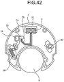
- FIG. 42 is a plan view illustrating a condition where devices are disposed on the substrate according to the tenth variation of the embodiment.
- the ground layer 70 is only required to be disposed in the region where the image antenna 9i is formed, and the shape and placement of the ground layer 70 are not limited to the shape and placement illustrated in the embodiment and other variations.
- the ground layer 70 according to the tenth variation is formed over the almost whole of the substrate 7 except a region required for wiring.
- the substrate 7 has wirings 78, 79, and 80.
- the wirings 78, 79, and 80 are conductive films formed on the substrate 7.
- the wiring 78 connects the connecting part 93 and the connecting part 96 of the antenna 9 to the receiving circuit 15.
- the wiring 79 connects the control circuit 14 to the drive source 56. Note that, in FIG. 42 , the illustration of the wirings 79 and 80 is omitted.
- the wiring 80 connects between other various circuits 57 (see FIG. 42 ) disposed on the substrate 7.
- the various circuits 57 include, for example, an oscillator circuit.
- the ground layer 70 is formed over the almost whole of the substrate 7 to surround these wirings 78, 79, and 80.
- the ground layer 70 may be individually disposed on a plurality of layers of the substrate 7.
- the ground layer 70 is stacked and disposed on the layers including the front surface 7a of the substrate 7. Disposing the ground layer 70 having a large area in this way enables the reception sensitivity of the antenna 9 to be further improved.
- the data included in a radio wave that the radio wave watch 1 transmits and receives is not limited to data including time information for correcting time.
- the data included in the radio wave to be transmitted and received may be a data signal, such as control program data and measurement data.
Landscapes
- Physics & Mathematics (AREA)
- General Physics & Mathematics (AREA)
- Engineering & Computer Science (AREA)
- Power Engineering (AREA)
- Radar, Positioning & Navigation (AREA)
- Remote Sensing (AREA)
- Electric Clocks (AREA)
- Electromechanical Clocks (AREA)
Abstract
Description
- The present invention relates to a radio wave watch.
- Conventional watches have an antenna.
Patent Literature 1 discloses the technology of a watch device that has a housing configured with a metal concave container and where, in addition to a watch operating part, a reverse F antenna for receiving a radio wave from a GPS satellite is disposed in the concave part of the housing. - Patent Literature 1: Japanese Patent Application Laid-Open No.
2012-75090 - There is room for improving the reception sensitivity of an antenna.
- An object of the present invention is to provide a radio wave watch that can improve the reception sensitivity of an antenna.
- A radio wave watch according to the present invention includes an exterior case; a dial plate disposed within the exterior case; a substrate disposed on a rear side of the dial plate within the exterior case; a first ground layer disposed on the substrate; an antenna that has a planar emitting electrode disposed between a center of the exterior case and an inner wall surface of the exterior case and opposed to the first ground layer, a planar short-circuit part electrically connecting an end part of the emitting electrode to the first ground layer, and a connecting part connecting the emitting electrode to a receiving circuit of the substrate; and a second ground layer disposed on an opposite side to the emitting electrode side across the short-circuit part on the substrate and having a width equal to or greater than a width of the short-circuit part.
- A radio wave watch according to the present invention has a second ground layer disposed on an opposite side to an emitting electrode side across a short-circuit part on a substrate and having a width equal to or greater than a width of the short-circuit part. The second ground layer improves the symmetricity of an antenna and an image antenna and improves the reception sensitivity of the antenna. The radio wave watch according to the present invention thus exhibits its effect of enabling the reception sensitivity of the antenna and improve the reception sensitivity.
-
-
FIG. 1 is a plan view illustrating a radio wave watch according to an embodiment. -
FIG. 2 is a sectional view of the radio wave watch according to the embodiment. -
FIG. 3 is a sectional view of a main part of the radio wave watch according to the embodiment. -
FIG. 4 is a perspective view of an antenna according to the embodiment. -
FIG. 5 is an illustrative view of an image antenna. -
FIG. 6 is a perspective view illustrating a first placement of the antenna. -
FIG. 7 is a perspective view illustrating a second placement of the antenna. -
FIG. 8 is a view illustrating the sensitivity of the antenna in the first placement and the second placement. -
FIG. 9 is a perspective view illustrating a configuration where a ground layer is extended in the first placement. -
FIG. 10 is a perspective view illustrating a configuration where a ground layer is extended in the second placement. -
FIG. 11 is a view illustrating a measurement result of the reception sensitivity in the first placement. -
FIG. 12 is a view illustrating a measurement result of the reception sensitivity in the second placement. -
FIG. 13 is a perspective view illustrating a configuration having a surrounding metal cover in the first placement. -
FIG. 14 is a perspective view illustrating a configuration having the surrounding metal cover in the second placement. -
FIG. 15 is a view illustrating a measurement result of the reception sensitivity in the first placement. -
FIG. 16 is a view illustrating a measurement result of the reception sensitivity in the second placement. -
FIG. 17 is a plan view illustrating a placement example of a solar cell. -
FIG. 18 is a plan view illustrating a placement example of a date plate. -
FIG. 19 is a plan view illustrating another placement example of the antenna. -
FIG. 20 is a perspective view illustrating one example of the shape of the antenna. -
FIG. 21 is a sectional view illustrating the solar cell disposed to overlap with a second region. -
FIG. 22 is a plan view illustrating a radio wave watch according to a first variation of the embodiment. -
FIG. 23 is a perspective view of an antenna according to the first variation of the embodiment. -
FIG. 24 is a front view of the antenna according to the first variation of the embodiment. -
FIG. 25 is a side view describing the directivity of the antenna. -
FIG. 26 is a perspective view illustrating one example of the shape of the antenna. -
FIG. 27 is a perspective view illustrating another example of the antenna. -
FIG. 28 is a plan view of a radio wave watch according to a second variation of the embodiment. -
FIG. 29 is a plan view of a radio wave watch according to a third variation of the embodiment. -
FIG. 30 is a plan view of a radio wave watch according to a fourth variation of the embodiment. -
FIG. 31 is a sectional view of a radio wave watch according to a fifth variation of the embodiment. -
FIG. 32 is a sectional view of a main part of a radio wave watch according to a sixth variation of the embodiment. -
FIG. 33 is a plan view of an antenna according to a seventh variation of the embodiment. -
FIG. 34 is a plan view of an antenna according to an eighth variation of the embodiment. -
FIG. 35 is a perspective view of the antenna according to the eighth variation of the embodiment. -
FIG. 36 is a front view of the antenna according to the eighth variation of the embodiment. -
FIG. 37 is a plan view illustrating a placement example of the antenna according to the eighth variation of the embodiment. -
FIG. 38 is a plan view illustrating one example of a shape of the solar cell. -
FIG. 39 is a plan view illustrating another placement example of the antenna. -
FIG. 40 is a plan view illustrating a placement of a motor according to a ninth variation of the embodiment. -
FIG. 41 is a plan view illustrating a placement of a ground layer according to a tenth variation of the embodiment. -
FIG. 42 is a plan view illustrating a condition where a device is disposed on a substrate according to the tenth variation of the embodiment. - A radio wave watch according to an embodiment of the present invention will now be described in detail with reference to the drawings. Note that this invention is not limited by this embodiment. Components in the following embodiment include components that those skilled in the art can conceive of easily or substantially the same as those.
- An embodiment will be described with reference to
FIGS. 1 to 21 . The present embodiment relates to a radio wave watch.FIG. 1 is a plan view illustrating a radio wave watch according to the embodiment;FIG. 2 is a sectional view of the radio wave watch according to the embodiment;FIG. 3 is a sectional view of a main part of the radio wave watch according to the embodiment;FIG. 4 is a perspective view of an antenna according to the embodiment; andFIG. 5 is an illustrative view of an image antenna. A section II-II inFIG. 1 is illustrated inFIG. 2 . - As illustrated in
FIGS. 1 and2 , a radio wave watch 1 of the embodiment has anexterior case 2, awindshield 3, adial plate 4, ahand 5, asolar cell 6, asubstrate 7, abattery 8, anantenna 9, and arear cover 10. Note that the illustration of thewindshield 3, thedial plate 4, thehand 5, and thesolar cell 6 is omitted inFIG. 1 . Theradio wave watch 1 receives a radio wave from a satellite. Theradio wave watch 1 has a function to correct its internal time based on information acquired from the radio wave. The radio wave watch 1 of the present embodiment receives a global positioning system (GPS) radio wave output from a GPS satellite. Note that the GPS radio wave is a radio wave including GPS time information and uses, for example, two types of a 1.5 GHz band (1575.42 MHz) and a 1.2 GHz band (1227.60 MHz). - The
exterior case 2 is a member constituting the shell of theradio wave watch 1. For example, theexterior case 2 is formed of a conductive material, such as titanium and titanium alloys. Theexterior case 2 has an approximatelycylindrical body part 21 and alug 22. Thebody part 21 is a cylindrical constituent part where both ends in an axial direction are opened. Thelug 22 is formed integrally with thebody part 21 and projects from the circumferential surface of thebody part 21 toward the outside in a radial direction. A belt is coupled to thelug 22. - In the present specification, the direction of a center axis line X1 of the
body part 21 is referred to as an "axial direction". The axial direction corresponds to a vertical direction of theradio wave watch 1. Furthermore, a direction perpendicular to the center axis line X1 is referred to as a "radial direction", and a circumferential direction centered at the center axis line X1 is referred to as a "circumferential direction". In the radial direction, a side near the center axis line X1 is referred to as the "inside", and a side far from the center axis line X1 is referred to as the "outside". - The
windshield 3 blocks an opening on the front side of thebody part 21. Thewindshield 3 is formed of a transparent material, such as glass. Thewindshield 3 covers thedial plate 4 and thehand 5 on the front side. Therear cover 10 blocks an opening on the back side of thebody part 21. Therear cover 10 is a plate-shaped member and, for example, is formed of metal. Therear cover 10 covers thesubstrate 7 on the back side. - The
exterior case 2 has anaccommodating space 23, the sectional shape of which is generally circular. Theaccommodating space 23 is an inner space of thebody part 21. Theaccommodating space 23 is a closed space surrounded by thebody part 21, thewindshield 3, and therear cover 10. Theaccommodating space 23 accommodates thedial plate 4, thehand 5, thesolar cell 6, thesubstrate 7, thebattery 8, and theantenna 9. - The
dial plate 4 is a disk-shaped member and fixed to thebody part 21. Thedial plate 4 is configured so that thedial plate 4 can pass light from the front side to the back side. For example, thedial plate 4 is formed of an optically transparent material. For example, thedial plate 4 may be formed of a non-conductive material, such as a synthetic resin. - The
hand 5 has asecond hand 51, aminute hand 52, and anhour hand 53. Thehand 5 is disposed coaxially with the center axis line X1 of theexterior case 2. Arotation shaft 55 of thehand 5 is passed through a through hole of thedial plate 4. Each of thesecond hand 51, theminute hand 52, and thehour hand 53 is coupled to a drive source, such as a motor, through awheel train 54. Thewheel train 54 is disposed on the back side relative to thedial plate 4 and decelerates the rotation of adrive source 56 to convey it to thehand 5. Thedrive source 56 of the present embodiment is a step motor. Thedrive source 56 rotationally drives thehand 5 with power supplied from thebattery 8. - The
solar cell 6 is disposed on the back surface of thedial plate 4. Thesolar cell 6 is formed into a plane shape. Thesolar cell 6 converts received light into electric energy. Thesolar cell 6 is an aggregate of photovoltaic elements, and its front side is a light-receiving surface. Thesolar cell 6 generates electricity with light penetrating thedial plate 4. Thesolar cell 6 is electrically connected with thesubstrate 7. The power generated by thesolar cell 6 may be supplied to devices of theradio wave watch 1, or may be charged into thebattery 8. - The
substrate 7 is disposed in the vicinity of therear cover 10 in theaccommodating space 23. Thesubstrate 7 is fixed to a main plate, which is not shown, and the main plate is fixed to thebody part 21. Thesubstrate 7 is disposed separately on the back side from thedial plate 4 in the axial direction and is opposed to thedial plate 4. Thesubstrate 7 is a component of a controller controlling theradio wave watch 1. Thesubstrate 7 has acontrol circuit 14 and a receivingcircuit 15. Thecontrol circuit 14 controls driving of thedrive source 56 and corrects the internal time. The receivingcircuit 15 is connected with theantenna 9. The receivingcircuit 15 decodes a satellite signal received by theantenna 9 to generate a digital signal. The digital signal generated by the receivingcircuit 15 is sent to thecontrol circuit 14. Thecontrol circuit 14 corrects the internal time based on the signal acquired from the receivingcircuit 15. Thecontrol circuit 14 can correct display time of thehand 5 based on the internal time. Furthermore, thecontrol circuit 14 has, in a storage region, geographic data where location information is associated with time zones and, from a result of the satellite reception, can determine a time zone to which a current location belongs to reflect it on the watch. - A
ground layer 70 is disposed on thesubstrate 7. For example, theground layer 70 may be formed of a ground plate formed of a conductive material, a ground electrode film formed on thesubstrate 7, or other components. The position and shape of theground layer 70 is determined depending on the position and shape of theantenna 9. As discussed below, theground layer 70 of the present embodiment is disposed to be opposed to theantenna 9 and animage antenna 9i (seeFIG. 5 ). Theground layer 70 of the present embodiment is formed on afront surface 7a of thesubstrate 7. Theground layer 70 is electrically connected with theexterior case 2. The electrical connection may be either direct-current connection or alternate-current connection. Theground layer 70 may be connected with theexterior case 2 via an inner layer of thesubstrate 7. Note that theground layer 70 may be electrically connected with therear cover 10 instead of theexterior case 2. - The shape of the
ground layer 70 of the present embodiment is rectangular. Theground layer 70 has afirst side 70a, asecond side 70b, athird side 70c, and afourth side 70d. Thefirst side 70a is a side facing aninner wall surface 21a of theexterior case 2. Thefirst side 70a and thefourth side 70d are opposed to each other in the radial direction. Thesecond side 70b and thethird side 70c are opposed to each other in the circumferential direction. - For example, the
ground layer 70 is disposed so that a foot of aperpendicular line 70p drawn from the center axis line X1 to thefirst side 70a is the center of thefirst side 70a or a position in the vicinity of the center. In this case, each of thesecond side 70b and thethird side 70c of theground layer 70 is parallel to the perpendicular line. In theground layer 70 of the present embodiment, thefirst side 70a is a short side, and thesecond side 70b and thethird side 70c are long sides. Thefirst side 70a is slightly shorter than thesecond side 70b and thethird side 70c. Note that the length of thefirst side 70a may be equal to the length of thesecond side 70b and thethird side 70c. - As illustrated in
FIG. 1 , a width WG of theground layer 70 is greater than a width WE of an emittingelectrode 91 described below. In the present embodiment, the width WG of theground layer 70 is greater than the width WE of the emittingelectrode 91 and is smaller than the width WB of abase part 94. Note that, in the present embodiment, a width WS of a short-circuit part 92 (seeFIG. 4 ) is equal to the width WE of the emittingelectrode 91. The width WG of theground layer 70 is thus greater than the width WS of the short-circuit part 92. However, the width WG of theground layer 70 may be equal to the width WS of the short-circuit part 92. - As illustrated in
FIG. 3 , thefourth side 70d of theground layer 70 is located at an inside end part in the radial direction of theantenna 9. More specifically, thefourth side 70d is located inside in the radial direction relative to the inside end part in the radial direction of the emittingelectrode 91. Thus, the short-circuit part 92 is disposed between thefirst side 70a and thefourth side 70d of theground layer 70. The emittingelectrode 91 is disposed between the short-circuit part 92 and thefourth side 70d on theground layer 70. As illustrated inFIG. 1 , the emittingelectrode 91 is disposed between thesecond side 70b and thethird side 70c of theground layer 70. Note that thefourth side 70d may be located inside relative to the inside end part in the radial direction of theantenna 9. - The
antenna 9 is disposed on thesubstrate 7. More specifically, theantenna 9 is disposed on thefront surface 7a of thesubstrate 7. Theantenna 9 is disposed between the center axis line X1 and theinner wall surface 21a of theexterior case 2. Theantenna 9 has the emittingelectrode 91, the short-circuit part 92, a connectingpart 93, and thebase part 94. - The
base part 94 is formed, of a dielectric, into a cubic shape. For example, thebase part 94 is formed of a non-conductive dielectric, such as a ceramic. Thebase part 94 is configured with a material having a high dielectric constant, such as zirconia or titanium oxide, and exhibits a wavelength-shortening effect. The shape of thebase part 94 of the present embodiment is a rectangular parallelepiped. Thebase part 94 enables a substantial wavelength λ' of a radio wave that the emittingelectrode 91 receives to be smaller than a wavelength λ corresponding to the frequency of the GPS radio wave. - As illustrated in
FIG. 4 , thebase part 94 is disposed so that afront surface 94a faces the front side, or thefront surface 94a is opposed to thewindshield 3. Thebase part 94 is disposed so that afirst side surface 94c is opposed to theinner wall surface 21a of theexterior case 2 and asecond side surface 94d faces the center axis line X1 side. Thefirst side surface 94c and thesecond side surface 94d are side surfaces located across thefront surface 94a and face in mutually opposite directions. Thebase part 94 of the present embodiment is disposed so that the position of a foot of aperpendicular line 94e drawn from the center axis line X1 to thesecond side surface 94d is the center position in a width direction of thesecond side surface 94d. The shape of theantenna 9 is symmetric with reference to the perpendicular line drawn from the center axis line X1 to the foot of theperpendicular line 94e. Note that thefirst side surface 94c and thesecond side surface 94d of the present embodiment are side surfaces along the long side of thefront surface 94a. - The
ground layer 70 is formed so that thefourth side 70d (seeFIG. 3 ) is parallel to thesecond side surface 94d of thebase part 94 and thefirst side 70a is parallel to thefirst side surface 94c of thebase part 94. Thebase part 94 is disposed in an inside region in the radial direction of theground layer 70. - The emitting
electrode 91 is disposed on thefront surface 94a of thebase part 94. The emittingelectrode 91 is a planar constituent part formed of a material having conductivity, such as metal. The emittingelectrode 91, as well as the short-circuit part 92 and the connectingpart 93 described below may be configured with a conductive-material thin film formed on the dielectric, which is thebase part 94, or may be configured with a plate-shaped member. Note that theantenna 9 illustrated in the present embodiment is the one where a thin film is formed on the dielectric, but, instead of this, theantenna 9 may be configured only with a conductive plate-shaped member, or may be configured by combining thebase part 94 with the conductive plate-shaped member. Examples of theplanar emitting electrode 91 include both the one configured with a thin film and the one formed into a plate shape. Also, examples of the planar short-circuit part 92 and the connectingpart 93 include both the ones configured with a thin film and the ones formed into a plate shape. Furthermore, theplanar emitting electrode 91, the short-circuit part 92, and the connectingpart 93 also includes a configuration where they have an uneven part on the whole or part of their surfaces. - The shape of the emitting
electrode 91 of the present embodiment is rectangular. The emittingelectrode 91 is disposed, on thefront surface 94a, to cover a most region of thefront surface 94a. The emittingelectrode 91 is disposed to expose an edge part of thefront surface 94a in a U shape. More specifically, a partial region inside in the radial direction of thefront surface 94a and regions at both ends in the width direction thereof are exposed. Each side of the emittingelectrode 91 is parallel to the corresponding side of thefront surface 94a. Note that the emittingelectrode 91 may be provided to prevent the exposure of thefront surface 94a, in other words, cover the whole of thefront surface 94a. - Note that, in the description of the
antenna 9 and theground layer 70 in the present specification, the "width direction" is a direction perpendicular to an extension direction of the emittingelectrode 91. For example, the emittingelectrode 91 of the present embodiment extends from the short-circuit part 92 along the radial direction. The "extension direction" in this case is a direction of the perpendicular line that links the center axis line X1 to the line of theperpendicular line 70p. The width direction is a direction perpendicular to this perpendicular line, and, for example, a direction parallel to thefirst side 70a of theground layer 70. - The emitting
electrode 91 has first emittingsides emitting side 91b. The first emittingsides 91a are sides along the radial direction of the emittingelectrode 91. One of the first emittingsides 91a and the other of the first emittingsides 91a are generally parallel or substantially parallel. The secondemitting side 91b is a side substantially perpendicular to the first emittingsides 91a of the emittingelectrode 91, in other words, a side along the width direction. The substantial antenna length of the emittingelectrode 91 is the length of a side from apoint 91c, to which the short-circuit part 92 is connected, to the second emittingside 91b, i.e., the length of the first emittingsides electrode 91 is formed so that, for example, the antenna length is a length of 1/4 of the substantial wavelength λ' after shortening. Theantenna 9 of the present embodiment has characteristics of a planar monopole antenna. More specifically, in theantenna 9 of the present embodiment, each of the first emittingsides sides sides - The short-
circuit part 92 is disposed on thefirst side surface 94c of thebase part 94. Thefirst side surface 94c is a surface facing outside in the radial direction of thebase part 94. The short-circuit part 92 is a planar constituent part formed of a material having conductivity, such as metal. For example, the shape of the short-circuit part 92 is rectangular. The short-circuit part 92 extends from the upper end of thefirst side surface 94c to the lower end thereof. The short-circuit part 92 is disposed to expose both end parts in the width direction of thefirst side surface 94c. The upper end of the short-circuit part 92 leads to the emittingelectrode 91 and is electrically connected with the emittingelectrode 91. The lower end of the short-circuit part 92 is electrically connected with theground layer 70. In the present embodiment, the width WS of the short-circuit part 92 is equal to the width WE of the emittingelectrode 91. - The connecting
part 93 is disposed on thesecond side surface 94d of thebase part 94. Thesecond side surface 94d is a surface facing inside in the radial direction of thebase part 94. The connectingpart 93 is a planar constituent part formed of a material having conductivity, such as metal. For example, the shape of the connectingpart 93 is rectangular. The connectingpart 93 extends from an end part on aback surface 94b side of thesecond side surface 94d to a position relatively on the front side as compared with the center. The connectingpart 93 is an RF connecting part and connected to the receivingcircuit 15. In theantenna 9 of the present embodiment, the connectingpart 93 is capacitively coupled to the emittingelectrode 91. The connectingpart 93 and the emittingelectrode 91 are separated without physical contact. The capacitive coupling of the connectingpart 93 and the emittingelectrode 91 achieves non-contact-type signal transmission. Impedance matching is achieved based on the distance between an end part on the front side of the connectingpart 93 and the second emittingside 91b. Note that power may be supplied by directly connecting the connectingpart 93 with the emittingelectrode 91. - The
base part 94 is supported by thesubstrate 7 so that itsback surface 94b contacts with theground layer 70. Theback surface 94b is opposed to an inside region in the radial direction of theground layer 70. Thefirst side surface 94c of thebase part 94 is parallel to thefirst side 70a of theground layer 70, and thesecond side surface 94d of thebase part 94 is parallel to thefourth side 70d of theground layer 70. To prevent theground layer 70 from being electrically connected with the connectingpart 93, the connectingpart 93 and a connected electrode 75 (seeFIG. 3 ) are disposed at a predetermined distance to theground layer 70. The connectingpart 93 is connected to the receivingcircuit 15 via theelectrode 75. It is preferable for theelectrode 75 to be made as small as possible in terms of reducing influence on the impedance of theantenna 9. Furthermore, it is preferable for the distance between theelectrode 75 and theground layer 70 to be separated as far as possible. Furthermore, it is preferable for theelectrode 75 and theground layer 70 not to overlap in a planar manner. - As illustrated in
FIG. 3 and other figures, theground layer 70 of the present embodiment has afirst region 71 and asecond region 72. Thefirst region 71 is an inside region in the radial direction relative to the short-circuit part 92. Thesecond region 72 is an outside region in the radial direction relative to the short-circuit part 92. Thefirst region 71 and thesecond region 72 are continuous and constitute thesingle ground layer 70. In theground layer 70 of the present embodiment, the shape of thefirst region 71 and the shape of thesecond region 72 are the same. That is to say, theground layer 70 has a symmetric shape with reference to the short-circuit part 92. More specifically, a length LG1 of thefirst region 71 in the radial direction is equal to a length LG2 of thesecond region 72 in the radial direction. Also, the width of thefirst region 71 and the width of thesecond region 72 are the same. Thus, the area of thefirst region 71 is equal to the area of thesecond region 72. - As described with reference to
FIG. 5 , the radio wave watch 1 of the present embodiment enables the reception sensitivity of theantenna 9 to be improved with theimage antenna 9i. Theimage antenna 9i is a virtual antenna and paired with theantenna 9. It is thought that theimage antenna 9i is generated on the opposite side to the emittingelectrode 91 side across the short-circuit part 92. Theimage antenna 9i is generated in a shape symmetric to theantenna 9 and at a position symmetric to it with reference to the short-circuit part 92. - The
image antenna 9i includes avirtual electrode 91i. Thevirtual electrode 91i is a virtual constituent part formed, by an image effect, at the position symmetric to the emittingelectrode 91 with reference to the short-circuit part 92. Thevirtual electrode 91i extends from the short-circuit part 92 toward the outside in the radial direction and is opposed to thesecond region 72 of theground layer 70. - In the present embodiment, no components are disposed in the space part where the
image antenna 9i is generated. In other words, the exclusive space for generating theimage antenna 9i is secured. Furthermore, theground layer 70 is symmetrically formed with reference to the short-circuit part 92. That is, the electrical symmetricity between the inside region in the radial direction and the outside region in the radial direction is secured with reference to the short-circuit part 92. This generates theimage antenna 9i having high symmetricity to theantenna 9. As a result, the radio wave watch 1 of the present embodiment enables the reception sensitivity of theantenna 9 to be improved to the maximum. However, a mounted object may be disposed in the region where theimage antenna 9i is generated. Disposing the mounted object in the region for generating theimage antenna 9i enables a power-supplying line to the mounted object to be shortened, and can decrease the influence of wiring capacity and reducing propagation loss. - Referring to
FIGS. 6 to 16 , the reception sensitivity of theantenna 9 of the radio wave watch 1 of the present embodiment will be described. - One example of a placement of the
antenna 9 on theground layer 70 is illustrated inFIGS. 6 and 7 . Eachantenna 9 inFIGS. 6 and 7 is disposed at an end part of theground layer 70, and the positions of their short-circuit part 92 are different. In theantenna 9 illustrated inFIG. 6 , the short-circuit part 92 faces the central side of theground layer 70, similarly to the placement of the radio wave watch 1 of the present embodiment. In other words, theground layer 70 extends frontward from the short-circuit part 92, in the placement of theantenna 9 inFIG. 6 . A length LGX of theground layer 70 extending forward from the short-circuit part 92 is twice or more than a length LB of thebase part 94. - In contrast, the short-
circuit part 92 of theantenna 9 illustrated inFIG. 7 faces the opposite side to the central side of theground layer 70. In this case, noground layer 70 substantially exists forward from the short-circuit part 92. That is,FIGS. 6 and FIG. 7 have the difference of whether theground layer 70 is provided forward from the short-circuit part 92. In the following description, the placement of theantenna 9 inFIG. 6 is referred to as a "first placement", and the placement of theantenna 9 inFIG. 7 is referred to as a "second placement". -
FIG. 8 illustrates the sensitivity of theantenna 9 in the first placement and the second placement. InFIG. 8 , the vertical axis represents the reception sensitivity C/N [dB] of theantenna 9.FIG. 8 illustrates the sensitivity to a radio wave received from four GPS satellites. As is apparent fromFIG. 8 , the reception sensitivity in the first placement is better than the reception sensitivity in the second placement. That is, it is found that the reception sensitivity of theantenna 9 in the case where theground layer 70 exists forward from the short-circuit part 92 is improved as compared with the case where noground layer 70 exists. It is considered that this is because theground layer 70 forward from the short-circuit part 92 results in forming theimage antenna 9i having high symmetricity to theantenna 9. - Next, a change in the sensitivity in the case where the
ground layer 70 is added in the first placement and the second placement will be described.FIG. 9 is a view illustrating a configuration where the ground layer is extended in the first placement, andFIG. 10 is a perspective view illustrating a configuration where the ground layer is extended in the second placement. Theground layer 70 illustrated inFIGS. 9 and10 has anextension part 70X. Theextension part 70X is a part where the end part of theground layer 70, on the side where theantenna 9 is disposed, is extended. As illustrated inFIG. 9 , theextension part 70X in the first placement extends frontward from the connectingpart 93. In other words, the part, of theground layer 70, disposed forward from the short-circuit part 92 has no change from that inFIG. 6 . - In contrast, the
extension part 70X in the second placement extends forward from the short-circuit part 92, as illustrated inFIG. 10 . That is, theground layer 70 is added forward from the short-circuit part 92 as compared with the configuration inFIG. 7 . The length LX of theextension part 70X is similar to the length LB of thebase part 94. -
FIG. 11 illustrates a measurement result of the reception sensitivity in the first placement.FIG. 12 illustrates a measurement result of the reception sensitivity in the second placement.FIG. 11 illustrates, in the first placement, the reception sensitivity in the case where noextension part 70X is provided (FIG. 6 ) and the reception sensitivity in the case where theextension part 70X is provided (FIG. 9 ).FIG. 12 illustrates, in the second placement, the reception sensitivity in the case where noextension part 70X is provided (FIG. 7 ) and the reception sensitivity in the case where theextension part 70X is provided (FIG. 10 ). - As illustrated in
FIG. 11 , the presence or absence of theextension part 70X in the first placement has no large influence on the reception sensitivity of theantenna 9. In contrast, as illustrated inFIG. 12 , the presence or absence of theextension part 70X in the second placement have significant influence on the reception sensitivity of theantenna 9. In the case where theextension part 70X is provided, the reception sensitivity is significantly improved as compared with the case where noextension part 70X is provided. - As is apparent from the above result, disposing the
ground layer 70 on the opposite side to the emittingelectrode 91 side across the short-circuit part 92 improves the sensitivity of theantenna 9. It is considered that this improvement in the reception sensitivity arises from that theground layer 70 disposed forward from the short-circuit part 92 secures the symmetricity between theantenna 9 and theimage antenna 9i. That is to say, in theground layer 70, it is considered that the enhanced symmetricity of both sides across the short-circuit part 92 enables the reception sensitivity of theantenna 9 to be improved. - Next, the influence of a surrounding metal member on the reception sensitivity of the
antenna 9 will be described.FIG. 13 illustrates a configuration where ametal cover 12 is put on in the first placement.FIG. 14 illustrates a configuration where themetal cover 12 is put on in the second placement. Thecover 12 is a box-shaped member configured with metal having conductivity. Thecover 12 covers the surroundings of theground layer 70 and theantenna 9. Thecover 12 is electrically connected with theground layer 70. A height HC of thecover 12 is approximately twice the length LB of thebase part 94. -
FIG. 15 illustrates a measurement result of the reception sensitivity in the first placement.FIG. 16 illustrates a measurement result of the reception sensitivity in the second placement.FIG. 15 illustrates, in the first placement, the reception sensitivity in the case where nocover 12 is provided (FIG. 6 ) and the reception sensitivity in the case where thecover 12 is provided (FIG. 13 ).FIG. 16 illustrates, in the second placement, the reception sensitivity in the case where nocover 12 is provided (FIG. 7 ) and the reception sensitivity in the case where thecover 12 is provided (FIG. 14 ). - As illustrated in
FIG. 15 , the presence or absence of thecover 12 in the first placement have significant influence on the reception sensitivity of theantenna 9. In the case where thecover 12 is provided in the first placement, the reception sensitivity significantly drops as compared with the case where nocover 12 is provided. In contrast, the presence or absence of thecover 12 in the second placement has influence on the reception sensitivity to some extent. In the case where thecover 12 is provided in the second placement, the reception sensitivity also drops as compared with the case where nocover 12 is provided. However, the degree of drop in the reception sensitivity in the second placement is smaller than the degree of drop in the reception sensitivity in the first placement. That is, it is said that the second placement has high tolerance to the metal enclosure as compared with the first placement. - In the first placement, it is considered that the connecting
part 93, which is capacitively coupled to the emittingelectrode 91, is disposed near thecover 12, which is the metal member, and thus the reception sensitivity drops under the influence of the metal of thecover 12. - In the radio wave watch 1 of the present embodiment, each component is disposed so that the metal member does not cover the
antenna 9 and theimage antenna 9i from above. For example, as illustrated inFIGS. 3 and5 , thesolar cell 6 is disposed not to cover thesecond region 72 of theground layer 70 and theantenna 9 from above. More specifically, anend surface 6a of thesolar cell 6 is located inside in the radial direction relative to the emittingelectrode 91. That is, thesolar cell 6 is disposed not to overlap with at least the emittingelectrode 91 when viewed in the axial direction. The radio wave watch 1 of the present embodiment thus enables the reception sensitivity of theantenna 9 to be improved. - The
solar cell 6 may be configured as illustrated inFIG. 17. FIG. 17 is a plan view illustrating a placement example of the solar cell. The shape of thesolar cell 6 illustrated inFIG. 17 is a shape where a part of its disk is notched. Thesolar cell 6 has a sector-shapednotch part 6b. The width of thenotch part 6b becomes wider as it goes outside in the radial direction from the center axis line X1. The shape and placement of thenotch part 6b are determined so that thesolar cell 6 does not overlap with theantenna 9 and theground layer 70 when viewed in the axial direction. That is, thenotch part 6b is formed so that thesolar cell 6 does not shield the front side of theantenna 9 and theground layer 70. - Note that a non-conductive member may be disposed on the front side of the
ground layer 70.FIG. 18 is a plan view illustrating a placement example of a date plate. In the case where adate plate 13 disposed in theradio wave watch 1 is a non-conductive member, thedate plate 13 may overlap with theground layer 70 when viewed in the axial direction. For example, thedate plate 13 is disposed coaxially with the center axis line X1. For example, thedate plate 13 is disposed to overlap with thesecond region 72 of theground layer 70 and not to overlap with theantenna 9. In other words, thedate plate 13 is disposed outside in the radial direction relative to theantenna 9. It is considered that the non-conductive member is unlikely to affect the symmetricity between theantenna 9 and theimage antenna 9i even when it is disposed at a position opposed to theground layer 70. However, in view of the thickness of the whole watch, it is preferable for it to be disposed not to overlap with theantenna 9. - Another placement example of the
antenna 9 will be described.FIG. 19 is a plan view illustrating another placement example of the antenna. In the placement illustrated inFIG. 19 , the short-circuit part 92 of theantenna 9 is disposed to face in the circumferential direction. In other words, the emittingelectrode 91 extends from the short-circuit part 92 along the circumferential direction, in the placement illustrated inFIG. 19 . Thesecond region 72 of theground layer 70 extends from theantenna 9 toward the opposite side to the emittingelectrode 91 side along the circumferential direction. - For example, the
antenna 9 is disposed so that the short-circuit part 92 is located on a virtual plane S1. The virtual plane S1 is a plane including the center axis line X1. In other words, theantenna 9 is disposed so that the short-circuit part 92 extends along the virtual plane S1 in the radial direction. In this case, theground layer 70 is disposed to be symmetric with reference to the virtual plane S1. That is, in theground layer 70, thefirst region 71 and thesecond region 72 are located on the different sides across the virtual plane S1. - The placement as illustrated in
FIG. 19 also enables the reception sensitivity of theantenna 9 to be improved by the effect of theimage antenna 9i. - Another shape of the
antenna 9 will be described.FIG. 20 is a perspective view illustrating one example of the shape of the antenna. In theantenna 9 illustrated inFIG. 20 , thefirst side surface 94c of thebase part 94 is an inclined surface. Thefirst side surface 94c is inclined to approach thesecond side surface 94d as it goes from theback surface 94b side to thefront surface 94a side. The short-circuit part 92 is inclined similarly to thefirst side surface 94c. Various shapes other than the illustrated one can be adopted as the shape of theantenna 9. - As discussed above, the radio wave watch 1 according to the present embodiment has the
exterior case 2, thedial plate 4, thesubstrate 7, thefirst region 71 of theground layer 70, theantenna 9, and thesecond region 72 of theground layer 70. Thedial plate 4 is disposed within theexterior case 2. Thefirst region 71 of theground layer 70 corresponds to a first ground layer disposed on thesubstrate 7. Theantenna 9 is disposed between the center axis line X1, which is the center of theexterior case 2, and theinner wall surface 21a of theexterior case 2. Theantenna 9 has theplanar emitting electrode 91, the planar short-circuit part 92, and the connectingpart 93. The emittingelectrode 91 is opposed to thefirst region 71 of theground layer 70. The short-circuit part 92 electrically connects the end part of the emittingelectrode 91 with thefirst region 71 of theground layer 70. The connectingpart 93 connects the emittingelectrode 91 with the receivingcircuit 15 of thesubstrate 7. - The
second region 72 of theground layer 70 corresponds to a second ground layer disposed on thesubstrate 7. Thesecond region 72 is disposed on the opposite side to the emittingelectrode 91 side across the short-circuit part 92 on thesubstrate 7. The width WG of thesecond region 72 is equal to or greater than the width WS of the short-circuit part 92. Theantenna 9 of the present embodiment improves, with thesecond region 72 of theground layer 70, the symmetricity between theimage antenna 9i and theantenna 9. Thus, theantenna 9 of the present embodiment can achieve improving its reception sensitivity. - In the
antenna 9 of the present embodiment, thefirst region 71 as the first ground layer and thesecond region 72 as the second ground layer are integrated with each other. The integration of thefirst region 71 and thesecond region 72 facilitates improving the symmetricity between theimage antenna 9i and theantenna 9. Furthermore, the configuration of theground layer 70 is simplified. - In the
antenna 9 of the present embodiment, the emittingelectrode 91 extends from the short-circuit part 92 toward the radial direction, which is a direction perpendicular to the center axis line X1 of theexterior case 2. Such a placement easily secures the symmetricity of the emittingelectrode 91 in positional relationship with theinner wall surface 21a of theexterior case 2. - In the
antenna 9 of the present embodiment, thesecond region 72 of theground layer 70 extends from the short-circuit part 92 toward the opposite side to the emittingelectrode 91 side. The length LG2 of thesecond region 72 in this extension direction is equal to or greater than a length LE of the emittingelectrode 91. Thus, thesecond region 72 of the present embodiment can improve the symmetricity between theimage antenna 9i and theantenna 9. - Note that the length LG2 of the
second region 72 may be less than the length LE of the emittingelectrode 91. For example, the length LG2 of thesecond region 72 is determined depending on the size of a region to be secured. In theground layer 70, the shape of thefirst side 70a may be an arc shape corresponding to the shape of theinner wall surface 21a of theexterior case 2, instead of the straight shape. This enables a limited space to be effectively utilized to enhance the symmetricity between thefirst region 71 and thesecond region 72. - In the
antenna 9 of the present embodiment, the metal member is disposed in a region not overlapping with the emittingelectrode 91 in the direction of the center axis line X1 of theexterior case 2, in the space between thedial plate 4 and thesubstrate 7. For example, thesolar cell 6 is disposed in the region not overlapping with the emittingelectrode 91 when viewed in the axial direction, as illustrated inFIG. 17 . Thedrive source 56 and thewheel train 54 are also disposed in the region not overlapping with the emittingelectrode 91 when viewed in the axial direction. Disposing the metal member in the region not overlapping with the emittingelectrode 91 enables the reception sensitivity of theantenna 9 to be improved. - In the
antenna 9, the metal member may be disposed in a region overlapping with thesecond region 72. The metal member disposed in the region overlapping with thesecond region 72 is, for example, thesolar cell 6, thedrive source 56, a magnetic shield, and thewheel train 54.FIG. 21 illustrates thesolar cell 6 disposed to overlap with thesecond region 72. Thesolar cell 6 is opposed to thesecond region 72 of theground layer 70 in the axial direction. Thesolar cell 6 has anopening part 6c at a position opposed to the emittingelectrode 91. For example, the shape of theopening part 6c is rectangular. Theopening part 6c is provided in a range overlapping with the emittingelectrode 91 when viewed in the axial direction. The opening width and the opening length of theopening part 6c may be greater than the width WE and the length LE of the emittingelectrode 91, respectively. Disposing thesolar cell 6 also in the region overlapping with thesecond region 72 can achieve maximizing the light-receiving area of thesolar cell 6 while achieving improvement in the reception sensitivity of theantenna 9. - Note that, in
FIG. 21 , thesolar cell 6 overlaps with the whole region of thesecond region 72, but it is not limited to this. Thesolar cell 6 may overlap with a partial region of thesecond region 72. In thesolar cell 6, the region overlapping with thesecond region 72 may have an opening, a slit, or other empty spaces. For example, a part of theopening part 6c may be formed to overlap with thesecond region 72 when viewed in the axial direction. - The
solar cell 6 of theantenna 9 may have thenotch part 6b as illustrated inFIG. 17 . In the case where thesolar cell 6 is disposed between thedial plate 4 and thesubstrate 7, it is preferable for thesolar cell 6 to be disposed without causing the drop in the reception sensitivity of theantenna 9. Thesolar cell 6 illustrated inFIG. 17 has thenotch part 6b at a position opposed to the emittingelectrode 91 and thesecond region 72. Thenotch part 6b includes a range overlapping with the emittingelectrode 91 and thesecond region 72 when viewed in the axial direction. Thesolar cell 6 does not shield the front side of the emittingelectrode 91 and thesecond region 72, so that the drop in the reception sensitivity of theantenna 9 is reduced. - In the space between the
dial plate 4 and thesubstrate 7, a non-conductive member may be disposed to be opposed to thesecond region 72. For example, in the case where thewheel train 54 is a non-conductive member, thewheel train 54 may be disposed to be opposed to thesecond region 72. The non-conductive member is disposed to be opposed to thesecond region 72 in this way, so that the space between thesecond region 72 and thedial plate 4 is effectively utilized. Furthermore, the non-conductive member unlikely affects the characteristics of theimage antenna 9i. This enables the limited space within theexterior case 2 to be effectively utilized while achieving improvement in the reception sensitivity of theantenna 9. - The
radio wave watch 1 may have a planar, non-conductive rotating member opposed to thesubstrate 7, for example, the date plate and a day plate. In this case, it is preferable for this rotating member to be disposed not to overlap with the emittingelectrode 91 and disposed to overlap with thesecond region 72, in the direction of the center axis line X1 of theexterior case 2. For example, thedate plate 13 illustrated inFIG. 18 is disposed in the outermost periphery in the inner space of theexterior case 2. The inner periphery of thedate plate 13 is located, at least, outside in the radial direction relative to the emittingelectrode 91. Furthermore, a part of thedate plate 13 overlaps with thesecond region 72 of theground layer 70 when viewed in the axial direction. Such a placement can achieve enlarging thedate plate 13 in diameter while reducing the influence on the reception sensitivity of theantenna 9. - The connecting
part 93 of the present embodiment connects the emittingelectrode 91 with the receivingcircuit 15 by capacitive coupling. The connectingpart 93 is disposed at a position that is closer to the center of theexterior case 2 than the short-circuit part 92 is. The connectingpart 93 is far from theinner wall surface 21a of theexterior case 2, so that the capacitive coupling between the connectingpart 93 and the emittingelectrode 91 is unlike to be affected by theexterior case 2. - Note that, in the present embodiment, the antenna center of the
antenna 9 is disposed on the straight line that links the center of thebattery 8 to the center axis line X1, but this placement is one example. In the example of the present embodiment, the center of theantenna 9 is disposed at the position of approximately 12 o'clock, and the center of thebattery 8 is disposed at the position of approximately 6 o'clock. Instead of this, the center of theantenna 9 may be disposed at a position between 9 o'clock and 11 o'clock, and the center of thebattery 8 may be disposed at a position between 4 o'clock and 6 o'clock. - Note that, in the
ground layer 70, the shape of thefirst region 71 may be different from the shape of thesecond region 72. The length LG1 of thefirst region 71 may be different from the length LG2 of thesecond region 72. For example, the length LG1 of thefirst region 71 may be greater than the length LG2 of thesecond region 72. - Not only the
antenna 9 receives the radio wave, but also it may be used for transmitting the radio wave. For example, theantenna 9 may be used to perform transmission to and reception from peripheral equipment. In this case, theelectronic watch 1 may communicate with other equipment via short-distance wireless communication by, for example, Bluetooth (registered trademark) or Wi-Fi. In the case where theantenna 9 transmits the radio wave, power is supplied to the emittingelectrode 91 through the connectingpart 93. Theradio wave watch 1 may have a radio communication circuit including the receivingcircuit 15 and a transmitting circuit. In this case, the connectingpart 93 connects the radio communication circuit with the emittingelectrode 91. - With referring to
FIGS. 22 to 27 , a first variation of the embodiment will be described.FIG. 22 is a plan view illustrating a radio wave watch according to the first variation of the embodiment;FIG. 23 is a perspective view of an antenna according to the first variation of the embodiment;FIG. 24 is a front view of the antenna according to the first variation of the embodiment; andFIG. 25 is a side view describing the directivity of the antenna. Theantenna 9 of the first variation has a connectingpart 96 instead of the connectingpart 93 of the above embodiment. In the radio wave watch 1 of the first variation, the configuration other than theantenna 9 is similar to that of the above embodiment. The connectingpart 96 connects the receivingcircuit 15 to the emittingelectrode 91 physically and electrically. The connectingpart 96 is a planar constituent part and disposed on thefirst side surface 94c. The connectingpart 93 of the above embodiment indirectly connects the emittingelectrode 91 to the receivingcircuit 15 by capacitive coupling. In contrast, the connectingpart 96 of the first variation directly connects the emittingelectrode 91 to the receivingcircuit 15. In the first variation, thefirst side surface 94c faces inside in the radial direction. - The
antenna 9 of the first variation has a paired short-circuit parts circuit parts first side surface 94c. The paired short-circuit parts part 96 on both sides of the connectingpart 96. The paired short-circuit parts part 96 is disposed between the paired short-circuit parts part 96 and the paired short-circuit parts exterior case 2. That is, the connectingpart 96 and the paired short-circuit parts - The connecting
part 96, and the paired short-circuit parts electrode 91 side. That is, the connectingpart 96, and the paired short-circuit parts - In the
antenna 9 of the first variation, as illustrated inFIG. 24 , the direction of a current Ia flowing through the connectingpart 96 and the direction of a current Ib flowing through the short-circuit part 95 are opposite to each other. Thus, in the case where power is supplied to the emittingelectrode 91, a substantial power-supplying point is a power-supplyingpart 97 illustrated inFIG. 24 . The direction of the current Ia and the direction of the current Ib are opposite to each other and cancelled mutually, so that the connectingpart 96 fails to contribute to substantial emission. That is, the connectingpart 96 functions as a transmission path that fails to contribute to emission. Thus, as illustrated inFIG. 25 , the emittingelectrode 91 of theantenna 9 mainly contributes to emission. Theantenna 9 has its directivity along the axial direction as illustrated inFIG. 25 . That is, theantenna 9 can receive a radio wave traveling along the axial direction with high sensitivity. - As illustrated in
FIG. 23 , each of the paired short-circuit parts circuit parts circuit part 95 is greater than a width WP of the connectingpart 96. - As illustrated in
FIG. 22 , theantenna 9 is disposed so that the short-circuit part 95 and the connectingpart 96 face inside in the radial direction. The emittingelectrode 91 extends from the connectingpart 96 toward the outside in the radial direction. In other words, the emittingelectrode 91 extends from the connectingpart 96 toward theinner wall surface 21a of theexterior case 2 along the radial direction. - The
second region 72 of theground layer 70 is disposed inside in the radial direction relative to theantenna 9. Also in the first variation, the position of thesecond region 72 is the opposite position to the emittingelectrode 91 side across the short-circuit part 95 on thesubstrate 7. The width WG of thesecond region 72 is equal to or greater than the width WS1 of the short-circuit part 95. Similarly to the above embodiment, theground layer 70 has thefirst region 71 corresponding to theantenna 9. The shape of thefirst region 71 may be the same as that of thesecond region 72. It is preferable for the length LG2 of thesecond region 72 to be equal to or greater than the length LE of the emittingelectrode 91. - In the radio wave watch 1 of the first variation, the inside in the radial direction relative to the
antenna 9 is the region of theimage antenna 9i. Thesecond region 72 of theground layer 70 enhances the symmetricity between theantenna 9 and theimage antenna 9i. This improves the reception sensitivity of theantenna 9 also in the radio wave watch 1 of the first variation. - Note that the shape of the
antenna 9 may be a shape as illustrated inFIG. 26 . In theantenna 9 illustrated inFIG. 26 , thefirst side surface 94c of thebase part 94 is an inclined face. Thefirst side surface 94c is inclined to approach thesecond side surface 94d as it goes from theback surface 94b side to thefront surface 94a side. The short-circuit parts part 96 are inclined similarly to thefirst side surface 94c. - The emitting
electrode 91 may extend to a surface other than thefront surface 94a of thebase part 94. For example, as illustrated inFIG. 27 , the emittingelectrode 91 may extend from thefront surface 94a to thesecond side surface 94d. The extension of the emittingelectrode 91 over a plurality of surfaces can achieves downsizing theantenna 9. Various shapes other than the illustrated one can be adopted as the shape of theantenna 9. - In the radio wave watch 1 of the first variation, it is preferable for the metal member to be disposed in the region not overlapping with the emitting
electrode 91 in the direction of the center axis line X1. The metal member may be disposed in the region overlapping with thesecond region 72 of theground layer 70. Thesolar cell 6 may have a notch part at the position opposed to the emittingelectrode 91 and thesecond region 72. - The non-conductive member may be disposed to be opposed to the
second region 72 of theground layer 70. In the case where theradio wave watch 1 has a non-conductive rotating member, this rotating member may be disposed not to overlap with the emittingelectrode 91 and disposed to overlap with thesecond region 72, in the direction of the center axis line X1. - With referring to
FIG. 28 , a second variation of the embodiment will be described.FIG. 28 is a plan view of a radio wave watch according to the second variation of the embodiment. In the radio wave watch 1 of the second variation, thebattery 8 functions as the second ground layer. Thebattery 8 is disposed so that its negative electrode faces the front side. Theantenna 9 is disposed adjacently to thebattery 8 so that the short-circuit part 92 faces thebattery 8. Thebattery 8 is thus located on the opposite side to the emittingelectrode 91 across the short-circuit part 92. The negative electrode of thebattery 8 functions as the second ground layer and enables the symmetricity between theantenna 9 and theimage antenna 9i to be improved. - Note that the
antenna 9 of the above embodiment may be disposed adjacently to thebattery 8. In this case, theantenna 9 is disposed adjacently to thebattery 8 so that the paired short-circuit parts battery 8. Such a placement is advantageous in the case where it is difficult to secure a region of thesubstrate 7 for thesecond region 72. Note that, in the case where theantenna 9 is a direct-connection type, the connectingpart 96 of theantenna 9 may be disposed close to theexterior case 2 side, with theexterior case 2 set to the ground potential. In such a placement, theexterior case 2 also functions as thesecond region 72. For example, such a placement is effective in the case where it is difficult to secure a space on thesubstrate 7 for thesecond region 72. - With referring to
FIG. 29 , a third variation of the embodiment will be described.FIG. 29 is a plan view of a radio wave watch according to the third variation of the embodiment. Theantenna 9 of the third variation is disposed similarly to theantenna 9 of the above embodiment. Thesolar cell 6 of the third variation has a projectingpart 6d, which overlaps with theantenna 9 when viewed in the axial-direction. - The
solar cell 6 is provided with thenotch part 6b and has the projectingpart 6d at the center in the circumferential direction of thenotch part 6b. The projectingpart 6d extends from the center axis line X1 toward the outside in the radial direction. The projectingpart 6d is a rectangular constituent part having a constant width. The projectingpart 6d is disposed to overlap with a central part in the width direction of the emittingelectrode 91 and theground layer 70. The width of the projectingpart 6d is less than both the width WE of the emittingelectrode 91 and the width WG of theground layer 70. Thus, the projectingpart 6d does not overlap with the first emittingsides electrode 91. The projectingpart 6d overlaps with the central part of the second emittingside 91b when viewed in the axial-direction. The central part of the second emittingside 91b is a part where its potential fluctuation is smaller than that in the first emittingside 91a. Thus, even when the central part of the second emittingside 91b is shielded, this has no large influence on the reception sensitivity of the emittingelectrode 91. Thus, the projectingpart 6d can increase the light-receiving area of thesolar cell 6 while reducing the influence on the reception sensitivity of the emittingelectrode 91. - With referring to
FIG. 30 , a fourth variation of the embodiment will be described.FIG. 30 is a plan view of a radio wave watch according to the fourth variation of the embodiment. Theantenna 9 of the fourth variation is curved along the shape of theinner wall surface 21a of theexterior case 2. - As illustrated in
FIG. 30 , each of thefirst side surface 94c and thesecond side surface 94d of thebase part 94 is a curved surface having an arc shape. Each shape of thefirst side surface 94c and thesecond side surface 94d is an arc shape concentric with theinner wall surface 21a of theexterior case 2. The paired short-circuit parts part 96 are disposed along thefirst side surface 94c. That is, the paired short-circuit parts part 96 extend along a curved surface parallel to the center axis line X1. - The shape of the emitting
electrode 91 is a curved shape similar to thebase part 94. The shape of the second emittingside 91b is an arc shape concentric with theinner wall surface 21a of theexterior case 2. The first emittingsides 91a are inclined to approach mutually as they go inside in the radial direction. - The shape of the
ground layer 70 is a curved shape similar to thebase part 94. Each shape of thefirst side 70a and thefourth side 70d is an arc shape concentric with theinner wall surface 21a of theexterior case 2. Thesecond side 70b and thethird side 70c are inclined to approach mutually as they go inside in the radial direction. It is desirable that the curvature of the curved shape of theground layer 70 be a curvature where a distance from the center axis line X1 is assumed as a radius. Furthermore, in the case where a rotating member (e.g., a date plate) overlaps with thesecond region 72 of theground layer 70, it is preferable to match the curvature of the curved shape of theground layer 70 with the curvature of the rotating member. - The
antenna 9 is disposed in the outside region in the radial direction of theground layer 70. That is, the outside region in the radial direction of theground layer 70 is thefirst region 71, and the inside region in the radial direction is thesecond region 72. - Note that the first emitting
sides 91a of the emittingelectrode 91 may be parallel to each other. In this case, thesecond side 70b and thethird side 70c of theground layer 70 may be parallel. Instead of a direct power-supplying type of theantenna 9, theantenna 9 of the above embodiment, i.e., theantenna 9 where power is supplied to the emittingelectrode 91 by capacitive coupling may have a curved shape. In this case, theantenna 9 may be disposed in the inside region in the radial direction of theground layer 70. It is preferable for the connectingpart 93 to be disposed toward the inside in the radial direction. - With referring to
FIG. 31 , a fifth variation of the embodiment will be described.FIG. 31 is a sectional view of a radio wave watch according to the fifth variation of the embodiment. In the radio wave watch 1 of the fifth variation, afirst ground layer 73 and asecond ground layer 74 are separated. - The
ground layer 70 has thefirst ground layer 73 and thesecond ground layer 74. Thefirst ground layer 73 is disposed on thefront surface 7a of thesubstrate 7. In contrast, thesecond ground layer 74 is disposed within thesubstrate 7. Theground layer 70 is configured so that the potential of thefirst ground layer 73 is the same as that of thesecond ground layer 74. For example, thefirst ground layer 73 and thesecond ground layer 74 may be electrically connected via a through hole formed in thesubstrate 7. - The
second ground layer 74 is disposed on the opposite side to thefirst ground layer 73 across the short-circuit part 92. In the fifth variation, thefirst ground layer 73 is disposed inside in the radial direction relative to thesecond ground layer 74. In this way, thefirst ground layer 73 and thesecond ground layer 74 may be disposed in different layers in thesubstrate 7. This can contribute to downsizing and thinning because a mountedobject 16 having a physical height and theantenna 9 can be disposed on the same plane. Note that thefirst ground layer 73 and thesecond ground layer 74 may be disposed independently in the same layer of thesubstrate 7. Thesecond ground layer 74 may be disposed on the back side (therear cover 10 side) of thesubstrate 7. - A sixth variation of the embodiment will be described.
FIG. 32 is a sectional view of a main part of a radio wave watch according to the sixth variation of the embodiment. As illustrated inFIG. 32 , theantenna 9 is disposed to be embedded in thesubstrate 7. - The
ground layer 70 according to the sixth variation has afirst ground layer 76 and asecond ground layer 77. Thesubstrate 7 according to the sixth variation is a stacked substrate. For example, thefirst ground layer 76 is formed in the bottom layer. Here, the bottom layer is the most back-side layer in a stacked direction of thesubstrate 7. Thesubstrate 7 has aconcave part 7b to expose thefirst ground layer 76. Theantenna 9 is accommodated in theconcave part 7b. - The
second ground layer 77 is formed on thefront surface 7a of thesubstrate 7. Thesecond ground layer 77 is disposed on the opposite side to thefirst ground layer 76 across the short-circuit part 92. In other words, thesecond ground layer 77 is disposed on the opposite side to the emittingelectrode 91 across the short-circuit part 92. Thefirst ground layer 76 and thesecond ground layer 77 are electrically connected. The configuration of this variation contributes to thinning of the watch, for example. Note that thesecond ground layer 77 may be disposed in a middle layer or the bottom layer of thesubstrate 7, instead of thefront surface 7a. - A seventh variation of the embodiment will be described.
FIG. 33 is a plan view of an antenna according to the seventh variation of the embodiment. In the emittingelectrode 91 according to the seventh variation, the first emittingside 91a is formed into a meander shape. The firstemitting side 91a has continuously formed unevenness. Making the first emittingside 91a into the meander shape enables theantenna 9 to be downsized while securing a required antenna length. Note that, in addition to the first emittingside 91a or instead of the first emittingside 91a, the second emittingside 91b may be formed into a meander shape. - An eighth variation of the embodiment will be described.
FIG. 34 is a plan view of an antenna according to the eighth variation of the embodiment;FIG. 35 is a perspective view of the antenna according to the eighth variation of the embodiment;FIG. 36 is a front view of the antenna according to the eighth variation of the embodiment;FIG. 37 is a plan view illustrating a placement example of the antenna according to the eighth variation of the embodiment;FIG. 38 is a plan view illustrating one example of the shape of the solar cell; andFIG. 39 is a plan view illustrating another placement example of the antenna. In theantenna 9 according to the eighth variation, an intersection angle of the second emittingside 91b and the first emittingside 91a is different from a right angle. More specifically, the first emittingside 91a extends so that an intersection angle θ with the second emittingside 91b is an obtuse angle. Such an extension of the first emittingside 91a in a slanting direction can lengthen the length of the first emittingside 91a as compared with the case where the intersection angle θ is the right angle. As a result, theantenna 9 can be downsized while a required antenna length is secured. The shape of the emittingelectrode 91 of the eighth variation is a tapering shape in which its width becomes narrower as it goes from the base end to the tip. Here, the base end side of the emittingelectrode 91 is a side where the short-circuit part 95 and the connectingpart 96 are connected, i.e., thefirst side surface 94c side, and the tip side of the emittingelectrode 91 is thesecond side surface 94d side. - To improve the sensitivity of the
antenna 9, it is preferable for the area of the emittingelectrode 91 to be increased, for example. In this case, it is conceivable that thebase part 94 as a foundation is extended. On the other hand, the substantial wavelength λ' is shortened by the wavelength-shortening effect as the frame of thebase part 94 becomes larger. As a result, the most suitable length of the first emittingside 91a is shortened, and the extension of the area of the emittingelectrode 91 is limited. Theantenna 9 of the eighth variation can maximize the area of the emittingelectrode 91 and the length of the first emittingside 91a without excessively increasing the frame of thebase part 94. Note that the first emittingside 91a and the second emittingside 91b may be formed into a meander shape. In terms of obtaining stable characteristics of theantenna 9, it is desirable to secure the symmetricity between the inclined, paired first emittingsides - It is preferable for the width WS1 (see
FIG. 36 ) of the short-circuit part 95 to be increased in a feasible range, and it is preferable for the width WP of the connectingpart 96 to be decreased in a feasible range. As an example, the width WS1 of the short-circuit part 95 may be greater than the width WP of the connectingpart 96. Increasing the width WS1 of the short-circuit part 95 enhances, for example, the effect of the sensitivity improvement by theimage antenna 9i. Decreasing the width WP of the connectingpart 96 can decrease a width WN of theelectrode 75 of thesubstrate 7. Decreasing the width WN of theelectrode 75 reduces capacitive coupling of theelectrode 75 with another electrode of a circuit of thesubstrate 7 and other surrounding metal members. As a result, the impedance matching about theantenna 9 is facilitated. - For example, the
antenna 9 of the eighth variation is disposed as illustrated inFIG. 37 . Theantenna 9 inFIG. 37 is disposed so that the short-circuit part 95 and the connectingpart 96 face inside in the radial direction. That is, the connectingpart 96 is opposed to the center axis line X1 in the radial direction. Thebase part 94 may be disposed so that thesecond side surface 94d is close to theinner wall surface 21a. Thebase part 94 is disposed near theinner wall surface 21a, so that a space for placing other parts is easily secured in the vicinity of the center axis line X1. Furthermore, a space for theimage antenna 9i is easily secured inside in the radial direction relative to theantenna 9. - In the case where the shape of the emitting
electrode 91 is the tapering shape as in the eighth variation, thesolar cell 6 may have a shape as illustrated inFIG. 38 . In theelectronic watch 1 inFIG. 38 , thesolar cell 6 has anotch part 60 at a position opposed to theantenna 9. Thenotch part 60 is formed not to overlap with at least the emittingelectrode 91 in the axial direction. Thenotch part 60 has afirst side 60a,second sides sides - The
first side 60a is a side parallel to thefirst side surface 94c of thebase part 94. Thefirst side 60a is located inside in the radial direction relative to thefirst side surface 94c. Thesecond sides end surfaces base part 94. Thesecond sides inclined sides first side 60a to thesecond sides inclined sides first side 60a and thesecond sides inclined sides - In planar view, the
second sides side 91a of the emittingelectrode 91. Thesecond sides side 91a. More specifically, in planar view, thesecond sides side 91a as they go outside in the radial direction. Thesecond sides side 91a, so that currents flowing thesecond sides electrode 91. Thus, thesolar cell 6 of the eighth variation can achieve maximizing thesolar cell 6 while reducing the drop in the sensitivity of theantenna 9. - Note that the
antenna 9 may be disposed as illustrated inFIG. 39 . Theantenna 9 illustrated inFIG. 39 is disposed so that the short-circuit part 95 and the connectingpart 96 face outside in the radial direction. That is, the connectingpart 96 is opposed to theinner wall surface 21a of theexterior case 2 in the radial direction. This placement can increase the distance between the first emittingside 91a of the emittingelectrode 91 and theinner wall surface 21a. - A ninth variation of the embodiment will be described.
FIG. 40 is a plan view illustrating a placement of a motor according to the ninth variation of the embodiment. In theelectronic watch 1 according to the ninth variation, a part of amotor 11 is disposed at a position opposed to the short-circuit part 95 in the radial direction. Themotor 11 is an electromagnetic motor, and has a housing 11a, a coil 11b, and arotor 11c. Themotor 11 rotates therotor 11c with an induced electromotive force that is generated by powering the coil 11b. For example, themotor 11 is installed in theelectronic watch 1 as a drive source rotating the hand. Themotor 11 is disposed so that therotor 11c is located on the opposite side to theantenna 9 side relative to the coil 11b. - More specifically, the
antenna 9 of the ninth variation is disposed so that the short-circuit part 95 faces inside in the radial direction. Themotor 11 is disposed inside in the radial direction relative to theantenna 9. Themotor 11 is disposed so that therotor 11c is located inside in the radial direction relative to the coil 11b. The coil 11b thus extends between therotor 11c and theantenna 9. Theelectronic watch 1 has amagnetic shield 17. In planar view, themagnetic shield 17 covers therotor 11c. That is, themagnetic shield 17 shields therotor 11c in the axial direction. Themagnetic shield 17 of this variation is disposed to cover therotor 11c and not to cover theantenna 9. - As in the ninth variation, the
rotor 11c of themotor 11 is disposed apart from theantenna 9, so that themagnetic shield 17 can be disposed at a position with few influence on the emittingelectrode 91. As a result, themagnetic shield 17 is unlikely to cause the drop in the sensitivity of theantenna 9. Thus, the placement of the ninth variation achieves downsizing by disposing themotor 11 in the vicinity of theantenna 9 while reducing the drop in the sensitivity of theantenna 9 as far as possible. - A tenth variation of the embodiment will be described.
FIG. 41 is a plan view of a ground layer according to the tenth variation of the embodiment, andFIG. 42 is a plan view illustrating a condition where devices are disposed on the substrate according to the tenth variation of the embodiment. Theground layer 70 is only required to be disposed in the region where theimage antenna 9i is formed, and the shape and placement of theground layer 70 are not limited to the shape and placement illustrated in the embodiment and other variations. Theground layer 70 according to the tenth variation is formed over the almost whole of thesubstrate 7 except a region required for wiring. - As illustrated in
FIG. 41 , thesubstrate 7 has wirings 78, 79, and 80. Thewirings substrate 7. Thewiring 78 connects the connectingpart 93 and the connectingpart 96 of theantenna 9 to the receivingcircuit 15. Thewiring 79 connects thecontrol circuit 14 to thedrive source 56. Note that, inFIG. 42 , the illustration of thewirings wiring 80 connects between other various circuits 57 (seeFIG. 42 ) disposed on thesubstrate 7. Thevarious circuits 57 include, for example, an oscillator circuit. Theground layer 70 is formed over the almost whole of thesubstrate 7 to surround thesewirings ground layer 70 may be individually disposed on a plurality of layers of thesubstrate 7. For example, theground layer 70 is stacked and disposed on the layers including thefront surface 7a of thesubstrate 7. Disposing theground layer 70 having a large area in this way enables the reception sensitivity of theantenna 9 to be further improved. - An eleventh variation of the embodiment will be described. The data included in a radio wave that the radio wave watch 1 transmits and receives is not limited to data including time information for correcting time. The data included in the radio wave to be transmitted and received may be a data signal, such as control program data and measurement data.
- The contents disclosed in the embodiment and variations described above can be performed in combination as necessary.
-
- 1
- radio wave watch
- 2
- exterior case
- 3
- windshield
- 4
- dial plate
- 5
- hand
- 6
- solar cell
- 6a
- end surface
- 6b
- notch part
- 6c
- opening part
- 6d
- projecting part
- 7
- substrate
- 7a
- front surface
- 8
- battery
- 9
- antenna
- 10
- rear cover
- 11
- motor
- 12
- cover
- 13
- date plate
- 14
- control circuit
- 15
- receiving circuit
- 16
- mounted object
- 17
- magnetic shield
- 21
- body part
- 21a
- inner wall surface
- 22
- lug
- 23
- accommodating space
- 51
- second hand
- 52
- minute hand
- 53
- hour hand
- 54
- wheel train
- 55
- rotation shaft
- 56
- drive source
- 60
- notch part
- 70
- ground layer
- 70a
- first side
- 70b
- second side
- 70c
- third side
- 70d
- fourth side
- 70p
- foot of perpendicular line
- 70X
- extension part
- 71
- first region (first ground layer)
- 72
- second region (second ground layer)
- 73, 76
- first ground layer
- 74, 77
- second ground layer
- 75
- electrode
- 78, 79, 80
- wiring
- 91
- emitting electrode
- 91a
- first emitting side
- 91b
- second emitting side
- 92, 95
- short-circuit part
- 93, 96
- connecting part
- 94
- base part
- 94a
- front surface
- 94b
- back surface
- 94c
- first side surface
- 94d
- second side surface
- 94e
- foot of perpendicular line
- LE
- length of emitting electrode
- LG1
- length of first region
- LG2
- length of second region
- S1, S2
- virtual plane
- WG
- width of ground layer
- WE
- width of emitting electrode
- WB
- width of base part
- WP
- width of connecting part
- WS, WS1
- width of short-circuit part
- X1
- center axis line
Claims (12)
- A radio wave watch comprising:an exterior case;a dial plate disposed within the exterior case;a substrate disposed on a rear side of the dial plate within the exterior case;a first ground layer disposed on the substrate;an antenna that has a planar emitting electrode disposed between a center of the exterior case and an inner wall surface of the exterior case and opposed to the first ground layer, a planar short-circuit part electrically connecting an end part of the emitting electrode to the first ground layer, and a connecting part connecting the emitting electrode to a receiving circuit of the substrate; anda second ground layer disposed on an opposite side to the emitting electrode side across the short-circuit part on the substrate and having a width equal to or greater than a width of the short-circuit part.
- The radio wave watch according to claim 1, wherein
the first ground layer and the second ground layer are integrated with each other. - The radio wave watch according to claim 1 or 2, wherein
the emitting electrode extends from the short-circuit part toward a radial direction that is a direction perpendicular to a center axis line of the exterior case. - The radio wave watch according to any one of claims 1 to 3, wherein
the second ground layer extends from the short-circuit part toward the opposite side to the emitting electrode side, and
a length of the second ground layer in the extension direction is equal to or greater than a length of the emitting electrode in the extension direction. - The radio wave watch according to any one of claims 1 to 4, wherein
in a space between the dial plate and the substrate, a metal member is disposed in a region not overlapping with the emitting electrode in a direction of a center axis line of the exterior case. - The radio wave watch according to claim 5, wherein
the metal member is disposed in a region overlapping with the second ground layer. - The radio wave watch according to any one of claims 1 to 6, further comprising:a solar cell disposed between the dial plate and the substrate, whereinthe solar cell has a notch part at a position opposed to the emitting electrode and the second ground layer.
- The radio wave watch according to any one of claims 1 to 7, wherein
in a space between the dial plate and the substrate, a non-conductive member is disposed to be opposed to the second ground layer. - The radio wave watch according to any one of claims 1 to 8, further comprising:a plate-shaped, non-conductive rotating member opposed to the substrate, whereinthe rotating member is disposed not to overlap with the emitting electrode and disposed to overlap with the second ground layer, in a direction of a center axis line of the exterior case.
- The radio wave watch according to any one of claims 1 to 9, wherein
the connecting part physically and electrically connects the receiving circuit to the emitting electrode, and
the emitting electrode extends from the connecting part toward the inner wall surface of the exterior case. - The radio wave watch according to any one of claims 1 to 10, wherein
the connecting part physically and electrically connects the receiving circuit to the emitting electrode, and
the short-circuit part is disposed in line with the connecting part on both sides of the connecting part and extends along a plane parallel to a center axis line of the exterior case. - The radio wave watch according to any one of claims 1 to 9, wherein
the connecting part connects the emitting electrode to the receiving circuit by capacitive coupling, and
the connecting part is disposed at a position that is closer to the center of the exterior case than the short-circuit part is.
Applications Claiming Priority (2)
| Application Number | Priority Date | Filing Date | Title |
|---|---|---|---|
| JP2017194336 | 2017-10-04 | ||
| PCT/JP2018/034461 WO2019069673A1 (en) | 2017-10-04 | 2018-09-18 | Radio clock |
Publications (3)
| Publication Number | Publication Date |
|---|---|
| EP3693812A1 true EP3693812A1 (en) | 2020-08-12 |
| EP3693812A4 EP3693812A4 (en) | 2021-06-09 |
| EP3693812B1 EP3693812B1 (en) | 2022-12-14 |
Family
ID=65995382
Family Applications (1)
| Application Number | Title | Priority Date | Filing Date |
|---|---|---|---|
| EP18865087.3A Active EP3693812B1 (en) | 2017-10-04 | 2018-09-18 | Radio clock |
Country Status (5)
| Country | Link |
|---|---|
| US (1) | US11656582B2 (en) |
| EP (1) | EP3693812B1 (en) |
| JP (1) | JP7075410B2 (en) |
| CN (1) | CN111164519B (en) |
| WO (1) | WO2019069673A1 (en) |
Families Citing this family (6)
| Publication number | Priority date | Publication date | Assignee | Title |
|---|---|---|---|---|
| JP6907925B2 (en) * | 2017-03-29 | 2021-07-21 | セイコーエプソン株式会社 | Electronic clock |
| JP7107089B2 (en) * | 2018-08-20 | 2022-07-27 | セイコーエプソン株式会社 | electronic clock |
| JP7314689B2 (en) * | 2019-07-29 | 2023-07-26 | セイコーエプソン株式会社 | Clocks and clock control methods |
| JP7160066B2 (en) * | 2020-05-28 | 2022-10-25 | カシオ計算機株式会社 | Antenna receiving device and electronic clock |
| JP7708082B2 (en) * | 2022-11-30 | 2025-07-15 | カシオ計算機株式会社 | Electronic devices and electronic clocks |
| JPWO2025126354A1 (en) * | 2023-12-13 | 2025-06-19 |
Family Cites Families (17)
| Publication number | Priority date | Publication date | Assignee | Title |
|---|---|---|---|---|
| KR100533624B1 (en) * | 2002-04-16 | 2005-12-06 | 삼성전기주식회사 | Multi band chip antenna with dual feeding port, and mobile communication apparatus using the same |
| JP5493527B2 (en) * | 2009-07-14 | 2014-05-14 | セイコーエプソン株式会社 | Clock with wireless function |
| JP5564953B2 (en) | 2010-01-12 | 2014-08-06 | カシオ計算機株式会社 | ANTENNA DEVICE AND ELECTRONIC DEVICE |
| JP5413318B2 (en) * | 2010-07-05 | 2014-02-12 | セイコーエプソン株式会社 | Electronic clock |
| JP5764013B2 (en) | 2010-08-30 | 2015-08-12 | 学校法人智香寺学園 | Small electronic device |
| JP5598257B2 (en) * | 2010-10-28 | 2014-10-01 | カシオ計算機株式会社 | Electronics |
| JP6131532B2 (en) | 2012-05-29 | 2017-05-24 | セイコーエプソン株式会社 | Electronic equipment |
| JP6277665B2 (en) * | 2013-10-22 | 2018-02-14 | セイコーエプソン株式会社 | Portable device |
| JP6458437B2 (en) | 2014-10-09 | 2019-01-30 | セイコーエプソン株式会社 | Electronic clock |
| JP2016080350A (en) * | 2014-10-09 | 2016-05-16 | デンソクテクノ株式会社 | Measurement signal reception mechanism and automatic connection device |
| JP6459455B2 (en) * | 2014-12-04 | 2019-01-30 | セイコーエプソン株式会社 | Electronic clock |
| CN104536288A (en) | 2015-01-26 | 2015-04-22 | 成都天奥电子股份有限公司 | Satellite time service watch using novel antenna |
| JP6696195B2 (en) | 2015-08-06 | 2020-05-20 | セイコーエプソン株式会社 | Electronic clock |
| JP6888356B2 (en) * | 2017-03-21 | 2021-06-16 | セイコーエプソン株式会社 | Electronic clock |
| JP6947076B2 (en) * | 2018-02-22 | 2021-10-13 | セイコーエプソン株式会社 | Electronic clock |
| JP7107089B2 (en) * | 2018-08-20 | 2022-07-27 | セイコーエプソン株式会社 | electronic clock |
| JP7151453B2 (en) * | 2018-12-18 | 2022-10-12 | セイコーエプソン株式会社 | electronic clock |
-
2018
- 2018-09-18 WO PCT/JP2018/034461 patent/WO2019069673A1/en not_active Ceased
- 2018-09-18 CN CN201880064349.8A patent/CN111164519B/en active Active
- 2018-09-18 US US16/753,437 patent/US11656582B2/en active Active
- 2018-09-18 EP EP18865087.3A patent/EP3693812B1/en active Active
- 2018-09-18 JP JP2019546611A patent/JP7075410B2/en active Active
Also Published As
| Publication number | Publication date |
|---|---|
| WO2019069673A1 (en) | 2019-04-11 |
| JP7075410B2 (en) | 2022-05-25 |
| JPWO2019069673A1 (en) | 2020-11-05 |
| US20200319605A1 (en) | 2020-10-08 |
| EP3693812A4 (en) | 2021-06-09 |
| CN111164519B (en) | 2021-11-02 |
| US11656582B2 (en) | 2023-05-23 |
| CN111164519A (en) | 2020-05-15 |
| EP3693812B1 (en) | 2022-12-14 |
Similar Documents
| Publication | Publication Date | Title |
|---|---|---|
| EP3693812B1 (en) | Radio clock | |
| CN102467085B (en) | Electronic device equipped with antenna device and solar panel | |
| JP5170121B2 (en) | Electronics | |
| US11150612B2 (en) | Portable radio-controlled watch | |
| US8917213B2 (en) | Antenna device and electronic timepiece | |
| JP7073833B2 (en) | Electronic clock | |
| JP7107089B2 (en) | electronic clock | |
| JP2019056616A (en) | Portable radio clock | |
| JP7358873B2 (en) | Electronic clock with built-in antenna | |
| US11435701B2 (en) | Electronic watch | |
| JP6829131B2 (en) | Radio clock | |
| US11537083B2 (en) | Electronic timepiece | |
| JP6868500B2 (en) | Electronic clock | |
| US11145950B2 (en) | Electronic timepiece | |
| JP7103881B2 (en) | Electronic clock | |
| JP7022654B2 (en) | Radio clock | |
| JP7045267B2 (en) | Radio clock | |
| CN116805761A (en) | Antenna device and electronic timepiece | |
| JP7049928B2 (en) | Radio clock | |
| JP2011066648A (en) | Antenna device and radio wave receiving device | |
| US20230205142A1 (en) | Electronic Watch | |
| JP2019060672A (en) | Electronic watch | |
| JP6902982B2 (en) | Radio clock |
Legal Events
| Date | Code | Title | Description |
|---|---|---|---|
| STAA | Information on the status of an ep patent application or granted ep patent |
Free format text: STATUS: THE INTERNATIONAL PUBLICATION HAS BEEN MADE |
|
| PUAI | Public reference made under article 153(3) epc to a published international application that has entered the european phase |
Free format text: ORIGINAL CODE: 0009012 |
|
| STAA | Information on the status of an ep patent application or granted ep patent |
Free format text: STATUS: REQUEST FOR EXAMINATION WAS MADE |
|
| 17P | Request for examination filed |
Effective date: 20200331 |
|
| AK | Designated contracting states |
Kind code of ref document: A1 Designated state(s): AL AT BE BG CH CY CZ DE DK EE ES FI FR GB GR HR HU IE IS IT LI LT LU LV MC MK MT NL NO PL PT RO RS SE SI SK SM TR |
|
| AX | Request for extension of the european patent |
Extension state: BA ME |
|
| DAV | Request for validation of the european patent (deleted) | ||
| DAX | Request for extension of the european patent (deleted) | ||
| A4 | Supplementary search report drawn up and despatched |
Effective date: 20210512 |
|
| RIC1 | Information provided on ipc code assigned before grant |
Ipc: G04R 60/10 20130101AFI20210506BHEP Ipc: G04G 21/04 20130101ALI20210506BHEP Ipc: H01Q 1/44 20060101ALI20210506BHEP Ipc: H01Q 13/08 20060101ALI20210506BHEP |
|
| REG | Reference to a national code |
Ref country code: DE Ref legal event code: R079 Ref document number: 602018044357 Country of ref document: DE Free format text: PREVIOUS MAIN CLASS: G04R0060100000 Ipc: G04C0010020000 |
|
| GRAP | Despatch of communication of intention to grant a patent |
Free format text: ORIGINAL CODE: EPIDOSNIGR1 |
|
| STAA | Information on the status of an ep patent application or granted ep patent |
Free format text: STATUS: GRANT OF PATENT IS INTENDED |
|
| INTG | Intention to grant announced |
Effective date: 20220826 |
|
| RIC1 | Information provided on ipc code assigned before grant |
Ipc: H01Q 9/42 20060101ALI20220815BHEP Ipc: H01Q 5/378 20150101ALI20220815BHEP Ipc: H01Q 1/27 20060101ALI20220815BHEP Ipc: G04R 60/12 20130101ALI20220815BHEP Ipc: G04C 17/00 20060101ALI20220815BHEP Ipc: G04C 10/02 20060101AFI20220815BHEP |
|
| GRAS | Grant fee paid |
Free format text: ORIGINAL CODE: EPIDOSNIGR3 |
|
| GRAA | (expected) grant |
Free format text: ORIGINAL CODE: 0009210 |
|
| STAA | Information on the status of an ep patent application or granted ep patent |
Free format text: STATUS: THE PATENT HAS BEEN GRANTED |
|
| AK | Designated contracting states |
Kind code of ref document: B1 Designated state(s): AL AT BE BG CH CY CZ DE DK EE ES FI FR GB GR HR HU IE IS IT LI LT LU LV MC MK MT NL NO PL PT RO RS SE SI SK SM TR |
|
| REG | Reference to a national code |
Ref country code: GB Ref legal event code: FG4D |
|
| REG | Reference to a national code |
Ref country code: CH Ref legal event code: EP |
|
| REG | Reference to a national code |
Ref country code: DE Ref legal event code: R096 Ref document number: 602018044357 Country of ref document: DE |
|
| REG | Reference to a national code |
Ref country code: IE Ref legal event code: FG4D |
|
| REG | Reference to a national code |
Ref country code: AT Ref legal event code: REF Ref document number: 1538057 Country of ref document: AT Kind code of ref document: T Effective date: 20230115 |
|
| REG | Reference to a national code |
Ref country code: LT Ref legal event code: MG9D |
|
| REG | Reference to a national code |
Ref country code: NL Ref legal event code: MP Effective date: 20221214 |
|
| PG25 | Lapsed in a contracting state [announced via postgrant information from national office to epo] |
Ref country code: SE Free format text: LAPSE BECAUSE OF FAILURE TO SUBMIT A TRANSLATION OF THE DESCRIPTION OR TO PAY THE FEE WITHIN THE PRESCRIBED TIME-LIMIT Effective date: 20221214 Ref country code: NO Free format text: LAPSE BECAUSE OF FAILURE TO SUBMIT A TRANSLATION OF THE DESCRIPTION OR TO PAY THE FEE WITHIN THE PRESCRIBED TIME-LIMIT Effective date: 20230314 Ref country code: LT Free format text: LAPSE BECAUSE OF FAILURE TO SUBMIT A TRANSLATION OF THE DESCRIPTION OR TO PAY THE FEE WITHIN THE PRESCRIBED TIME-LIMIT Effective date: 20221214 Ref country code: FI Free format text: LAPSE BECAUSE OF FAILURE TO SUBMIT A TRANSLATION OF THE DESCRIPTION OR TO PAY THE FEE WITHIN THE PRESCRIBED TIME-LIMIT Effective date: 20221214 |
|
| REG | Reference to a national code |
Ref country code: AT Ref legal event code: MK05 Ref document number: 1538057 Country of ref document: AT Kind code of ref document: T Effective date: 20221214 |
|
| PG25 | Lapsed in a contracting state [announced via postgrant information from national office to epo] |
Ref country code: RS Free format text: LAPSE BECAUSE OF FAILURE TO SUBMIT A TRANSLATION OF THE DESCRIPTION OR TO PAY THE FEE WITHIN THE PRESCRIBED TIME-LIMIT Effective date: 20221214 Ref country code: LV Free format text: LAPSE BECAUSE OF FAILURE TO SUBMIT A TRANSLATION OF THE DESCRIPTION OR TO PAY THE FEE WITHIN THE PRESCRIBED TIME-LIMIT Effective date: 20221214 Ref country code: HR Free format text: LAPSE BECAUSE OF FAILURE TO SUBMIT A TRANSLATION OF THE DESCRIPTION OR TO PAY THE FEE WITHIN THE PRESCRIBED TIME-LIMIT Effective date: 20221214 Ref country code: GR Free format text: LAPSE BECAUSE OF FAILURE TO SUBMIT A TRANSLATION OF THE DESCRIPTION OR TO PAY THE FEE WITHIN THE PRESCRIBED TIME-LIMIT Effective date: 20230315 |
|
| PG25 | Lapsed in a contracting state [announced via postgrant information from national office to epo] |
Ref country code: NL Free format text: LAPSE BECAUSE OF FAILURE TO SUBMIT A TRANSLATION OF THE DESCRIPTION OR TO PAY THE FEE WITHIN THE PRESCRIBED TIME-LIMIT Effective date: 20221214 |
|
| PG25 | Lapsed in a contracting state [announced via postgrant information from national office to epo] |
Ref country code: SM Free format text: LAPSE BECAUSE OF FAILURE TO SUBMIT A TRANSLATION OF THE DESCRIPTION OR TO PAY THE FEE WITHIN THE PRESCRIBED TIME-LIMIT Effective date: 20221214 Ref country code: RO Free format text: LAPSE BECAUSE OF FAILURE TO SUBMIT A TRANSLATION OF THE DESCRIPTION OR TO PAY THE FEE WITHIN THE PRESCRIBED TIME-LIMIT Effective date: 20221214 Ref country code: PT Free format text: LAPSE BECAUSE OF FAILURE TO SUBMIT A TRANSLATION OF THE DESCRIPTION OR TO PAY THE FEE WITHIN THE PRESCRIBED TIME-LIMIT Effective date: 20230414 Ref country code: ES Free format text: LAPSE BECAUSE OF FAILURE TO SUBMIT A TRANSLATION OF THE DESCRIPTION OR TO PAY THE FEE WITHIN THE PRESCRIBED TIME-LIMIT Effective date: 20221214 Ref country code: EE Free format text: LAPSE BECAUSE OF FAILURE TO SUBMIT A TRANSLATION OF THE DESCRIPTION OR TO PAY THE FEE WITHIN THE PRESCRIBED TIME-LIMIT Effective date: 20221214 Ref country code: CZ Free format text: LAPSE BECAUSE OF FAILURE TO SUBMIT A TRANSLATION OF THE DESCRIPTION OR TO PAY THE FEE WITHIN THE PRESCRIBED TIME-LIMIT Effective date: 20221214 Ref country code: AT Free format text: LAPSE BECAUSE OF FAILURE TO SUBMIT A TRANSLATION OF THE DESCRIPTION OR TO PAY THE FEE WITHIN THE PRESCRIBED TIME-LIMIT Effective date: 20221214 |
|
| PG25 | Lapsed in a contracting state [announced via postgrant information from national office to epo] |
Ref country code: SK Free format text: LAPSE BECAUSE OF FAILURE TO SUBMIT A TRANSLATION OF THE DESCRIPTION OR TO PAY THE FEE WITHIN THE PRESCRIBED TIME-LIMIT Effective date: 20221214 Ref country code: PL Free format text: LAPSE BECAUSE OF FAILURE TO SUBMIT A TRANSLATION OF THE DESCRIPTION OR TO PAY THE FEE WITHIN THE PRESCRIBED TIME-LIMIT Effective date: 20221214 Ref country code: IS Free format text: LAPSE BECAUSE OF FAILURE TO SUBMIT A TRANSLATION OF THE DESCRIPTION OR TO PAY THE FEE WITHIN THE PRESCRIBED TIME-LIMIT Effective date: 20230414 Ref country code: AL Free format text: LAPSE BECAUSE OF FAILURE TO SUBMIT A TRANSLATION OF THE DESCRIPTION OR TO PAY THE FEE WITHIN THE PRESCRIBED TIME-LIMIT Effective date: 20221214 |
|
| REG | Reference to a national code |
Ref country code: DE Ref legal event code: R097 Ref document number: 602018044357 Country of ref document: DE |
|
| PLBE | No opposition filed within time limit |
Free format text: ORIGINAL CODE: 0009261 |
|
| STAA | Information on the status of an ep patent application or granted ep patent |
Free format text: STATUS: NO OPPOSITION FILED WITHIN TIME LIMIT |
|
| PG25 | Lapsed in a contracting state [announced via postgrant information from national office to epo] |
Ref country code: DK Free format text: LAPSE BECAUSE OF FAILURE TO SUBMIT A TRANSLATION OF THE DESCRIPTION OR TO PAY THE FEE WITHIN THE PRESCRIBED TIME-LIMIT Effective date: 20221214 |
|
| 26N | No opposition filed |
Effective date: 20230915 |
|
| PG25 | Lapsed in a contracting state [announced via postgrant information from national office to epo] |
Ref country code: SI Free format text: LAPSE BECAUSE OF FAILURE TO SUBMIT A TRANSLATION OF THE DESCRIPTION OR TO PAY THE FEE WITHIN THE PRESCRIBED TIME-LIMIT Effective date: 20221214 |
|
| REG | Reference to a national code |
Ref country code: DE Ref legal event code: R119 Ref document number: 602018044357 Country of ref document: DE |
|
| REG | Reference to a national code |
Ref country code: CH Ref legal event code: PL |
|
| PG25 | Lapsed in a contracting state [announced via postgrant information from national office to epo] |
Ref country code: LU Free format text: LAPSE BECAUSE OF NON-PAYMENT OF DUE FEES Effective date: 20230918 |
|
| REG | Reference to a national code |
Ref country code: BE Ref legal event code: MM Effective date: 20230930 |
|
| PG25 | Lapsed in a contracting state [announced via postgrant information from national office to epo] |
Ref country code: LU Free format text: LAPSE BECAUSE OF NON-PAYMENT OF DUE FEES Effective date: 20230918 Ref country code: MC Free format text: LAPSE BECAUSE OF FAILURE TO SUBMIT A TRANSLATION OF THE DESCRIPTION OR TO PAY THE FEE WITHIN THE PRESCRIBED TIME-LIMIT Effective date: 20221214 |
|
| REG | Reference to a national code |
Ref country code: IE Ref legal event code: MM4A |
|
| PG25 | Lapsed in a contracting state [announced via postgrant information from national office to epo] |
Ref country code: IE Free format text: LAPSE BECAUSE OF NON-PAYMENT OF DUE FEES Effective date: 20230918 |
|
| PG25 | Lapsed in a contracting state [announced via postgrant information from national office to epo] |
Ref country code: CH Free format text: LAPSE BECAUSE OF NON-PAYMENT OF DUE FEES Effective date: 20230930 |
|
| PG25 | Lapsed in a contracting state [announced via postgrant information from national office to epo] |
Ref country code: IE Free format text: LAPSE BECAUSE OF NON-PAYMENT OF DUE FEES Effective date: 20230918 Ref country code: FR Free format text: LAPSE BECAUSE OF NON-PAYMENT OF DUE FEES Effective date: 20230930 Ref country code: DE Free format text: LAPSE BECAUSE OF NON-PAYMENT OF DUE FEES Effective date: 20240403 Ref country code: CH Free format text: LAPSE BECAUSE OF NON-PAYMENT OF DUE FEES Effective date: 20230930 |
|
| PG25 | Lapsed in a contracting state [announced via postgrant information from national office to epo] |
Ref country code: BE Free format text: LAPSE BECAUSE OF NON-PAYMENT OF DUE FEES Effective date: 20230930 |
|
| PG25 | Lapsed in a contracting state [announced via postgrant information from national office to epo] |
Ref country code: BG Free format text: LAPSE BECAUSE OF FAILURE TO SUBMIT A TRANSLATION OF THE DESCRIPTION OR TO PAY THE FEE WITHIN THE PRESCRIBED TIME-LIMIT Effective date: 20221214 |
|
| PG25 | Lapsed in a contracting state [announced via postgrant information from national office to epo] |
Ref country code: BG Free format text: LAPSE BECAUSE OF FAILURE TO SUBMIT A TRANSLATION OF THE DESCRIPTION OR TO PAY THE FEE WITHIN THE PRESCRIBED TIME-LIMIT Effective date: 20221214 |
|
| PG25 | Lapsed in a contracting state [announced via postgrant information from national office to epo] |
Ref country code: CY Free format text: LAPSE BECAUSE OF FAILURE TO SUBMIT A TRANSLATION OF THE DESCRIPTION OR TO PAY THE FEE WITHIN THE PRESCRIBED TIME-LIMIT; INVALID AB INITIO Effective date: 20180918 |
|
| PG25 | Lapsed in a contracting state [announced via postgrant information from national office to epo] |
Ref country code: HU Free format text: LAPSE BECAUSE OF FAILURE TO SUBMIT A TRANSLATION OF THE DESCRIPTION OR TO PAY THE FEE WITHIN THE PRESCRIBED TIME-LIMIT; INVALID AB INITIO Effective date: 20180918 |
|
| PGFP | Annual fee paid to national office [announced via postgrant information from national office to epo] |
Ref country code: IT Payment date: 20250825 Year of fee payment: 8 |
|
| PGFP | Annual fee paid to national office [announced via postgrant information from national office to epo] |
Ref country code: GB Payment date: 20250731 Year of fee payment: 8 |
|
| PG25 | Lapsed in a contracting state [announced via postgrant information from national office to epo] |
Ref country code: TR Free format text: LAPSE BECAUSE OF FAILURE TO SUBMIT A TRANSLATION OF THE DESCRIPTION OR TO PAY THE FEE WITHIN THE PRESCRIBED TIME-LIMIT Effective date: 20221214 |