EP3691418A1 - Control device, illumination device, and program for control device - Google Patents
Control device, illumination device, and program for control device Download PDFInfo
- Publication number
- EP3691418A1 EP3691418A1 EP19219799.4A EP19219799A EP3691418A1 EP 3691418 A1 EP3691418 A1 EP 3691418A1 EP 19219799 A EP19219799 A EP 19219799A EP 3691418 A1 EP3691418 A1 EP 3691418A1
- Authority
- EP
- European Patent Office
- Prior art keywords
- pulse
- schedule
- timing
- pulses
- control device
- Prior art date
- Legal status (The legal status is an assumption and is not a legal conclusion. Google has not performed a legal analysis and makes no representation as to the accuracy of the status listed.)
- Granted
Links
Images



Classifications
-
- H—ELECTRICITY
- H05—ELECTRIC TECHNIQUES NOT OTHERWISE PROVIDED FOR
- H05B—ELECTRIC HEATING; ELECTRIC LIGHT SOURCES NOT OTHERWISE PROVIDED FOR; CIRCUIT ARRANGEMENTS FOR ELECTRIC LIGHT SOURCES, IN GENERAL
- H05B45/00—Circuit arrangements for operating light-emitting diodes [LED]
- H05B45/30—Driver circuits
- H05B45/32—Pulse-control circuits
- H05B45/325—Pulse-width modulation [PWM]
-
- H—ELECTRICITY
- H05—ELECTRIC TECHNIQUES NOT OTHERWISE PROVIDED FOR
- H05B—ELECTRIC HEATING; ELECTRIC LIGHT SOURCES NOT OTHERWISE PROVIDED FOR; CIRCUIT ARRANGEMENTS FOR ELECTRIC LIGHT SOURCES, IN GENERAL
- H05B45/00—Circuit arrangements for operating light-emitting diodes [LED]
- H05B45/20—Controlling the colour of the light
-
- H—ELECTRICITY
- H05—ELECTRIC TECHNIQUES NOT OTHERWISE PROVIDED FOR
- H05B—ELECTRIC HEATING; ELECTRIC LIGHT SOURCES NOT OTHERWISE PROVIDED FOR; CIRCUIT ARRANGEMENTS FOR ELECTRIC LIGHT SOURCES, IN GENERAL
- H05B45/00—Circuit arrangements for operating light-emitting diodes [LED]
- H05B45/40—Details of LED load circuits
- H05B45/44—Details of LED load circuits with an active control inside an LED matrix
- H05B45/46—Details of LED load circuits with an active control inside an LED matrix having LEDs disposed in parallel lines
-
- Y—GENERAL TAGGING OF NEW TECHNOLOGICAL DEVELOPMENTS; GENERAL TAGGING OF CROSS-SECTIONAL TECHNOLOGIES SPANNING OVER SEVERAL SECTIONS OF THE IPC; TECHNICAL SUBJECTS COVERED BY FORMER USPC CROSS-REFERENCE ART COLLECTIONS [XRACs] AND DIGESTS
- Y02—TECHNOLOGIES OR APPLICATIONS FOR MITIGATION OR ADAPTATION AGAINST CLIMATE CHANGE
- Y02B—CLIMATE CHANGE MITIGATION TECHNOLOGIES RELATED TO BUILDINGS, e.g. HOUSING, HOUSE APPLIANCES OR RELATED END-USER APPLICATIONS
- Y02B20/00—Energy efficient lighting technologies, e.g. halogen lamps or gas discharge lamps
- Y02B20/40—Control techniques providing energy savings, e.g. smart controller or presence detection
Definitions
- the present invention relates to a control device that outputs a plurality of pulses each having a duty set independently, an illumination device in which a light source is controlled by the control device, and a program for the control device.
- PWM pulse width modulation
- the PWM control described above is performed using a PWM function of a general-purpose microcomputer.
- a CPU of the microcomputer turns on (rises) a pulse and causes a timer to count time from on to off (fall) of the pulse based on the set duty.
- the CPU turns off the pulse, and then causes the timer to count the time from when the pulse is turned off to the end of one cycle of the pulse.
- the CPU then turns on the pulse again and repeats the above-described operation.
- the CPU is provided with a plurality of ports so that a plurality of pulses can be output.
- the duties of the plurality of pulses can be set optionally.
- the timers are required for the number of ports, and it is necessary to use an expensive CPU, which is a problem in terms of cost.
- the present invention has been made in view of the above-described circumstances, and an object thereof is to provide a control device, an illumination device, and a program for a control device in consideration of noise at low cost.
- a control device, an illumination device, and a program for a control device according to the present invention are characterized by the following [1] to [9].
- the plurality of pulses, each of which the duty is independently controlled can be output by the at least one timer.
- the off-timing of the first pulse is simultaneous with the on-timing of the second pulse, on/off states of the first and second pulses cancel each other, and an amount of change in a voltage of the pulse becomes gradual, so that high frequency noise can be reduced.
- the phases of the pulse of the first group and the pulse of the second group can be shifted by the half cycle, and the high frequency noise can be reduced in a state where the set duty is substantially maintained.
- the phases of the pulse of the first group and the pulse of the second group can be easily shifted by the half cycle.
- the plurality of light sources can be controlled.
- the program for the control device having the above configuration [10] can be easily executed by one control device.
- control device the illumination device, and the program for the control device in consideration of the noise at the low cost.
- the illumination device 1 of the present embodiment is a device configured to PWM-control a plurality of LEDs (light sources) 2 mounted in a vehicle interior of an automobile, for example. As shown in FIG. 1 , the illumination device 1 includes the plurality of LEDs 2, a plurality of FETQs, and the CPU 3 used as the control device.
- 18 LEDs 2 are provided.
- the plurality of LEDs 2 are provided with six full-color LEDs 21 to 26 configured by three-color LEDs 2 of red, green, and blue.
- the full-color LEDs 21 to 26 emit light in full color by adjusting brightness of the three-color LEDs 2.
- Anodes of the plurality of LEDs 2 are connected in common and are connected to a power source V.
- the plurality of FETQs are provided in the same number 18 as the plurality of LEDs 2, and the FETQs and the LEDs 2 are provided in a one-to-one correspondence.
- Each of the plurality of FETQs has a drain connected to a cathode of the corresponding LEDs 2, and a source connected to the ground.
- the CPU 3 as the control device outputs PWM controlled pulses from the plurality of ports ch1 to ch18, respectively. Gates of the FETQs are connected to the ports ch1 to ch18, respectively.
- the CPU 3 can adjust the brightness of each of the plurality of LEDs 2 independently by outputting the plurality of PWM controlled pulses. Accordingly, for example, colors of the full-color LEDs 21 to 26 can be adjusted manually by a user, or the colors of the full-color LEDs 21 to 26 can be automatically changed in accordance with a predetermined trigger such as when a door is opened and/or closed.
- the CPU 3 and the plurality of FETQs described above are incorporated in a housing of a connector C for connecting electric wires, such as a power supply line L1 and a ground line L2, to the LEDs 2.
- a communication line L3 is connected to the connector C, and the CPU 3 and an external control device can communicate with each other.
- the colors of the full-color LEDs 21 to 26 described above are changed manually or automatically at any timing as described above.
- a table showing a relationship between the colors and duties of the three-color LEDs 2 is stored in advance in a storage unit (not shown). Every time the color is changed, the CPU 3 obtains the duty of each of the three-color LEDs 2 corresponding to the changed color with reference to the table. Then, the CPU 3 changes a setting of the obtained duty as a duty of a pulse to be output to each of the three-color LEDs 2.
- the change in the setting of the duty using the above-described table may be performed by the external control device, and a result thereof may be transmitted to the CPU 3.
- the 18 ports ch1 to ch18 are provided in the CPU 3, but here, in order to simplify the description, an example in which a total of four ports chW, chX, chY and chZ are provided in the CPU 3, and duties 90%, 80%, 70% and 60% are respectively set to the ports chW, chX, chY and chZ will be described. In addition, it is assumed that the pulses output from the ports chW to chZ have the same frequency of 10000 ⁇ s.
- the CPU 3 creates a schedule in which on-timing and off-timing of the pulse are designated. More specifically, as shown in FIG. 2 , the CPU 3 divides the pulses from the ports chW to chZ into first and second groups G1, G2. In the present embodiment, the pulses from the ports chW, chX are set to the first group G1, and the pulses from the ports chY, chZ are set to the second group G2.
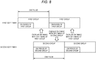
- the CPU 3 shifts phases of the pulse of the first group G1 and the pulse of the second group G2 by a half cycle. Accordingly, the CPU 3 can create the schedule in which the off-timing of the pulse of the first group G1 and the on-timing of the pulse of the second group G2 are simultaneous with each other, and the off-timing of the pulse of the second group G2 and the on-timing of the pulse of the first group G1 are simultaneous with each other.
- the creation of the schedule will be described with reference to an example shown in FIG. 2 .
- the CPU 3 alternately creates the schedule for the first group G1 and the schedule for the second group one pulse at a time.
- the CPU 3 outputs the pulses from the ports chW to chZ in accordance with the schedules created as described above.
- the CPU 3 performs the PWM control using two first and second soft timers that respectively count the on-timing of the first group G1 and the on-timing of the second group. Specifically, as shown in FIG. 2 , the CPU 3 sets the first soft timer to 100 ⁇ s, and sets the pulse from the port chW as a pulse to be first turned on. When the soft timer finishes counting 100 ⁇ s, the CPU 3 turns on the pulse from the port chW.
- the CPU 3 turns on the pulse from the port chX.
- the CPU 3 sequentially sets 8000 ⁇ s and 800 ⁇ s in the second soft timer, turns on the pulses from the ports chY, chZ, and simultaneously turns off the pulses from the ports chW, chX in accordance with the schedule created described above, every time the second soft timer counts the set time, and repeats the same operation as follows.
- Programs for a main processing shown in FIG. 3 and an interrupt processing shown in FIG. 4 are stored in a storage medium (not shown).
- the CPU 3 executes these programs to realize the main processing and the interrupt processing.
- the pulses output from the ports ch1 to ch18 described above are all output at the same cycle (for example, 10000 ⁇ s).
- the CPU 3 executes the main processing shown in FIG. 3 for each cycle of the pulse described above.
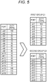
- the CPU 3 divides the plurality of pulses output from the ports ch1 to ch18 into first and second groups G1, G2 prior to the main processing and interrupt processing described above. At this time, the CPU 3 divides the number of pulses of the first group G1 into the same number as the number of pulses of the second group G2 as much as possible.
- the CPU 3 groups the first and second groups G1, G2 such that the numbers of pulses of the first and second groups G1, G2 are the same.
- the first and second groups G1, G2 are grouped such that the number of pulses of one of the first and second groups G1, G2 is larger than that of the other group by one.
- the CPU 3 sets the pulses from the ports ch1 to ch9 as the first group G1, and the pulses from the ports ch10 to ch18 as the second group G2.
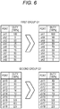
- the CPU 3 first determines whether or not the duty has just been changed in any one of the pulses from the ports ch1 to ch18 (step S1). In a case where it is determined that the duty has just been changed (that is, in a case where the main process is executed first after the duty is changed), as shown in FIG. 6 , the CPU 3 rearranges the first and second groups G1, G2 in an order of a value of the changed duty (step S2). Thereafter, the CPU 3 proceeds to step S3.
- step S3 the CPU 3 creates the schedule for the first group G1.
- the CPU 3 creates the schedule in which the on-timing is shifted at the constant interval in an arrangement order of all the pulses in the first group G1.
- the CPU 3 creates the schedule such that all the pulses of the first group G1 are turned on in the first half (0 ⁇ s to 5000 ⁇ s) of the one cycle.
- the CPU 3 creates the schedule in which the on-timing is shifted at the constant interval of 200 ⁇ s.
- the CPU 3 designates the on-timing of the pulse of the port ch1 having the largest duty among the first group G1 to, for example, 100 ⁇ s.
- the CPU 3 sets the on-timing of the pulses of the ports ch8, ch9, ..., and ch6 having the second, third, ... , and eighth largest duty to 300 ⁇ s, 500 ⁇ s, ... , and 1500 ⁇ s.
- the CPU 3 does not designate the on-timing of the pulse from the port ch2 having the duty of 0%.
- the CPU 3 obtains the off-timing of the pulses of all the ports ch1 to ch9 of the first group G1, creates the schedule for the first group G1, and ends step S3. Incidentally, the CPU 3 does not designate the off-timing for the pulse from the port ch1 having the duty of 100%. In addition, the CPU 3 designates the off-timing of the pulse from the port ch2 having the duty of 0% to 0 ⁇ s.
- the CPU 3 creates the schedule for the second group G2 such that the off-timing of the pulse designated in the schedule for the first group G1 created in step S3 becomes the on-timing (step S4), and ends the processing.
- the CPU 3 designates the on-timing of the pulses of the second group G2 to 0 ⁇ s, and designates the off-timing based on the set duties.
- the CPU 3 designates the off-timing of the pulses of all the ports ch10 to ch18 of the second group G2.
- the CPU 3 corrects the schedule for the second group G2 such that the off-timing of the pulses designated by the schedule for the first group G1 created in step S1 is simultaneous with the on-timing of the pulses of the second group G2.
- the CPU 3 creates the schedule such that all the pulses of the second group G2 are turned on in the latter half of the one cycle of the pulse of the first group G1 (5000 ⁇ s to 10000 ⁇ s).
- the pulses of the first group G1 turned off in the latter half of the one cycle are pulses from the ports ch8, ch9, ch7, ch5, and ch3.
- the CPU 3 selects the pulses from the ports ch8, ch9, ch7, ch5, and ch3 in the first group G1 as a "first pulse”.
- the schedule is created such that the pulse having a larger duty of the second group G2 is turned on at the off-timing of the pulse having a smaller duty of the first group G1.
- the pulse from the port ch11 of the second group G2 is designated as the on-timing of 6100 ⁇ s (the timing at which the pulse from the port ch3 of the first group G1 is turned off).
- the on-timing of the pulses from the ports ch10, ch12, ch13, and ch14 of the second group G2 are designated to 7900 ⁇ s, 8700 ⁇ s, 9000 ⁇ s, and 9300 ⁇ s that are the timing at which the pulses from the ports ch5, ch7, ch9, and ch8 of the first group G1 are turned off, respectively. That is, the CPU 3 selects the pulses from the ports ch11, ch10, ch12, ch13, and ch14 in the second group G2 as a "second pulse".
- the CPU 3 does not select the pulses from the ports ch4, ch6 that are turned off in the first half of the one cycle (0 ⁇ s to 5000 ⁇ s) as the "first pulse". That is, there is no pulse of the second group G2 turned on at the off-timing of the pulses from the ports ch4, ch6. As a result, as shown in FIG. 8 , the phases of the pulse of the first group G1 and the pulse of the second group G2 can be shifted by the half cycle.
- the pulses of the second group G2 include a "remaining pulse” (the pulses from the ports ch15, ch16, ch17, and ch18) that is not selected as the "second pulse", and of which the on-timing is not simultaneous with the off-timing of the pulse of the first group G1.
- the "remaining pulse” is designated by shifting the on-timing from the timing at which the pulse from the port ch14 is turned on (9300 ⁇ s) at the constant interval (for example, 200 ⁇ s). That is, for the pulses from the ports ch15, ch16, ch17, and ch18, 9500 ⁇ s, 9700 ⁇ s, 9900 ⁇ s, and 10100 ⁇ s are designated as the on-timing, respectively.
- the pulse from the port ch14 is a pulse having the latest on-timing among the pulses of the second group G2 of which the on-timing is simultaneous with the off-timing of the pulses of the first group G1.
- the CPU 3 designates the off-timing of the pulses from the ports ch9 to ch18 based on the set duties and the designated on-timing. Accordingly, the CPU 3 designates 10100 ⁇ s (6100 ⁇ s + one cycle ⁇ 0.4) as the off-timing with respect to the pulse from the port ch11. Similarly, the CPU 3 designates the off-timing for the ports ch10, ch12 to ch18, and ends the creation of the schedule for the second group G2. As described above, the CPU 3 functions as a first schedule creation section in steps S3 and S4.
- step S5 the CPU 3 creates the schedule for the first group G1 such that the off-timing of the pulse of the second group G2 in which the schedule is created in step S4 or step S6 of the previous main processing is simultaneous with the on-timing of the pulse of the first group G1.
- the CPU 3 creates the schedule such that all the pulses in the first group G1 is turned on in the latter half (10000 ⁇ s to 15000 ⁇ s) of the one cycle of the pulse of the second group G2 in which the schedule is created in step S4 or step S6 of the previous main processing.
- all the pulses in the second group G2 are turned off in the latter half (10000 ⁇ s to 15000 ⁇ s) of the one cycle.
- the CPU 3 creates the schedule such that the pulse having a smaller duty of the first group G1 is turned on at the off-timing of the pulse having a larger duty of the second group G2.
- the pulse from the port ch1 of the first group G1 is designated as the on-timing of 10390 ⁇ s (the timing at which the pulse from the port ch18 of the second group G2 is turned off).
- the on-timing of the pulses from the ports ch8, ch9, ch7, ch5, ch3, ch4, and ch6 of the first group G1 are designated to 10350 ⁇ s, 10680 ⁇ s, 10600 ⁇ s, 10600 us, 10400 us, 10700 us, and 10900 ⁇ s that are the timing at which the pulses from the ports ch17, ch16, ch15, ch14, ch13, ch12, and ch10 of the first group G2 are turned off, respectively.
- the CPU 3 does not designate the on-timing for the pulse from the port ch2 having the duty of 0%.
- the CPU 3 selects the pulses from the ports ch18, ch17, ch16, ch15, ch14, ch13, ch12, and ch10 of the second group G2 as the "first pulse", and the pulses from the ports ch1, ch8, ch9, ch7, ch5, ch3, ch4, and ch6 of the first group G1 are selected as the "second pulse”.
- the CPU 3 functions as a second schedule creation section.
- the CPU 3 creates the schedule for the second group G2 such that the off-timing of the pulse designated in the schedule for the first group G1 created in step S5 becomes the on-timing (step S6), and ends the processing. That is, in steps S5 and S6, the CPU 3 functions as the first schedule creation section. Since the processing of the CPU 3 in step S6 is the same as that in step S4 described above, a detailed description thereof is omitted here.
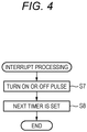
- the CPU 3 stops the above-described main processing every time the first or second soft timer finishes the counting, and executes the interrupt processing shown in FIG. 4 .
- the CPU 3 functions as a pulse output section, and turns on or off the pulses of the ports ch1 to ch18 set in step S8 to be described later (step S7).
- the CPU 3 functions as a setting section, and sets a pulse to be turned on or off next to the pulse that is turned on or off in step S7 in accordance with the schedule created in the previous cycle of the schedule that is currently created in the main processing (step S8).
- the CPU 3 sets the time until the set next pulse is turned on or off in the first or second soft timer (step S8), and ends the processing.
- the CPU 3 continues the main processing.
- step S8 as shown in FIG. 8 , the CPU 3 sets the time until the pulse of the first group G1 is turned on in the first soft timer, and sets the time until the pulse of the second group G2 is turned on in the second soft timer.
- the plurality of pulses of which the duties are independently controlled by the two first and second soft timers can be output.
- the off-timing of the first pulse selected from one of the first and second groups G1, G2 is simultaneous with the on-timing of the second pulse selected from the other of the first and second groups G1, G2, on/off states of the first and second pulses cancel each other, and an amount of change in a voltage of the pulse becomes gradual, so that high frequency noise can be reduced.
- the CPU 3 creates the schedule such that all the pulses of the group in which the first pulse is selected are turned on in the first half of the one cycle, and all the pulses of the group in which the second pulse is selected are turned on in the latter half of the one cycle of the first pulse. Accordingly, the phases of the pulse of the first group G1 and the pulse of the second group G2 can be shifted by the half cycle, and the high frequency noise can be reduced in a state where the set duties are substantially maintained.
- the CPU 3 does not select, as the first pulse, the pulse that is turned off in the first half of the one cycle in the group in which the first pulse is selected from the first and second groups G1, G2. Accordingly, the phases of the pulse of the first group G1 and the pulse of the second group G2 can be easily shifted by the half cycle.
- the CPU 3 create the schedule in which the on-timing of the remaining pulse (the pulses from the ports ch15 to ch18 in FIG. 7C ), that is not selected as the second pulse in the group in which the second pulse is selected from the first and second groups G1, G2, is shifted at the constant interval. Accordingly, since the on-timing of the remaining pulse can be shifted, the high frequency noise can be further reduced.
- the interrupt processing is executed by interrupting the main processing performed by the CPU 3. Accordingly, the program can be easily executed by one CPU 3.
- the soft timer is used as a timer, but a hard timer may be used.
- the CPU 3 arranges the pulses of the first and second groups G1, G2 in the order of values of the duties, but the present invention is not limited thereto.
- the arrangement order may be any order, and may be an order of arrangement of the ports ch1 to ch18.
- the CPU 3 is used for controlling the LEDs 2 (light source), but the present invention is not limited thereto.
- the CPU 3 may be used for PWM control of a load, and the load may be a heater or the like.
- the interrupt processing is executed using the first and second soft timers, but the present invention is not limited thereto.
- the interrupt processing may be executed using one soft timer.
Landscapes
- Circuit Arrangement For Electric Light Sources In General (AREA)
Abstract
Description
- The present invention relates to a control device that outputs a plurality of pulses each having a duty set independently, an illumination device in which a light source is controlled by the control device, and a program for the control device.
- Conventionally, a pulse width modulation (PWM) control has been used to control a light source of an automobile as a plurality of loads described above (Patent Literatures 1, 2). By controlling the light source by the PWM control, brightness of the light source can be easily changed. Specifically, the brightness can be adjusted by changing a pulse width for one cycle. In addition, by gradually changing to a target duty, the light source can be gradually brightened or darkened.
- The PWM control described above is performed using a PWM function of a general-purpose microcomputer. In the PWM function, a CPU of the microcomputer turns on (rises) a pulse and causes a timer to count time from on to off (fall) of the pulse based on the set duty. When the timer count ends, the CPU turns off the pulse, and then causes the timer to count the time from when the pulse is turned off to the end of one cycle of the pulse. When the timer count ends, the CPU then turns on the pulse again and repeats the above-described operation.
- The CPU is provided with a plurality of ports so that a plurality of pulses can be output. In addition, the duties of the plurality of pulses can be set optionally. However, with the use of the timer described above, the timers are required for the number of ports, and it is necessary to use an expensive CPU, which is a problem in terms of cost.
- In the PWM control described above, there is a problem that high frequency noise is generated when the pulse is turned on or off.
-
- Patent Literature 1:
JP-A-2007-290450 - Patent Literature 2:
JP-A-2004-186085 - The present invention has been made in view of the above-described circumstances, and an object thereof is to provide a control device, an illumination device, and a program for a control device in consideration of noise at low cost.
- In order to achieve the above object, a control device, an illumination device, and a program for a control device according to the present invention are characterized by the following [1] to [9].
- [1] A control device that outputs a plurality of pulses each having a duty set independently, the control device including:
- a schedule creation section configured to create a schedule in which on-timing and off-timing of the plurality of pulses are designated such that off-timing of a first pulse among the plurality of pulses and on-timing of a second pulse among the plurality of pulses are simultaneous with each other, based on the set duty and a cycle of the pulse;
- a setting section configured to set, in a timer for counting time, time from a time point where the timer finishes counting the time already set to on-timing or off-timing of a pulse to be first turned on or off after the time point in accordance with the schedule; and
- a pulse output section configured to turn on or off the pulse in accordance with the schedule when the timer finishes counting the set time.
- [2] The control device according to [1],
wherein the schedule creation section creates a schedule for the first pulse, and creates a schedule for the second pulse such that the off-timing of the first pulse designated by the schedule created for the first pulse and the on-timing of the second pulse are simultaneous with each other. - [3] The control device according to [1] or [2],
wherein the schedule creation section divides the plurality of pulses into first and second groups, and includes a first schedule creation section and a second schedule creation section,
wherein the first schedule creation section creates the schedule by selecting the first pulse from one of the first and second groups and selecting the second pulse from another of the first and second groups,
wherein the second schedule creation section creates the schedule by selecting the first pulse from the other of the first and second groups and selecting the second pulse from the one of the first and second groups, and
wherein the first schedule creation section and the second schedule creation section alternately create a schedule. - [4] The control device according to [3],
wherein the schedule creation section creates the schedule such that all the pulses of the group in which the first pulse is selected from the first and second groups are turned on in the first half of one cycle, and all the pulses of the group in which the second pulse is selected from the first and second groups are turned on in the latter half of the one cycle of the first pulse. - [5] The control device according to [3] or [4],
wherein the schedule creation section does not select, as the first pulse, the pulse that is turned off in the first half of the one cycle in the group in which the first pulse is selected from the first and second groups. - [6] The control device according to any one of [3] to [5],
wherein the schedule creation section creates the schedule in which on-timing of a remaining pulse, that is not selected as the second pulse in the group in which the second pulse is selected from the first and second group, is shifted at a constant interval. - [7] An illumination device including:
- the control device according to any one of claims 1 to 6; and
- a plurality of light sources controlled by a plurality of pulses output from the control device.
- [8] A control method for a control device executed by a control device that outputs a plurality of pulses each having a duty set independently, the control method including:
- a schedule creation step configured to create a schedule in which on-timing and off-timing of the plurality of pulses are designated such that off-timing of a first pulse among the plurality of pulses and on-timing of a second pulse among the plurality of pulses are simultaneous with each other, based on the set duty and a cycle of the pulse,
- a setting step configured to set, in a timer for counting time, time from a time point where the timer finishes counting the time already set to on-timing or off-timing of a pulse to be first turned on or off after the time point in accordance with the schedule, and
- a pulse output step configured to turn on or off the pulse in accordance with the schedule when the timer finishes counting the set time.
- [9] The control method according to [8],
wherein the setting step and the pulse output step are performed as an interrupt processing by interrupting the schedule creation section, every time the timer finishes counting the set time. - [10] A program for a control device executing the control method described in claim 8 or 9 by a computer.
- [11] A computer readable storage medium on which the program for the control device according to
claim 10 is stored. - According to the control device having the above configurations, the plurality of pulses, each of which the duty is independently controlled, can be output by the at least one timer. In addition, since the off-timing of the first pulse is simultaneous with the on-timing of the second pulse, on/off states of the first and second pulses cancel each other, and an amount of change in a voltage of the pulse becomes gradual, so that high frequency noise can be reduced.
- According to the control device having the above configuration [4], the phases of the pulse of the first group and the pulse of the second group can be shifted by the half cycle, and the high frequency noise can be reduced in a state where the set duty is substantially maintained.
- According to the control device having the above configuration [5], the phases of the pulse of the first group and the pulse of the second group can be easily shifted by the half cycle.
- According to the control device having the above configuration [6], since the on-timing of the remaining pulse can be shifted, the high frequency noise can be further reduced.
- According to the control device having the above configuration [7], the plurality of light sources can be controlled.
- According to the program for the control device having the above configuration [10], the program can be easily executed by one control device.
- According to the present invention, it is possible to provide the control device, the illumination device, and the program for the control device in consideration of the noise at the low cost.
- The present invention has been briefly described above. Further, details of the present invention will be clarified by reading a mode (hereinafter, referred to as "embodiment") for carrying out the invention to be described below with reference to accompanying drawings.
-
-
FIG. 1 is a circuit diagram showing an embodiment of an illumination device incorporating a CPU as a control device of the present invention. -
FIG. 2 is a time chart of pulses output from ports chW, chX, chY and chZ and time set in a timer for simply explaining an operation of the illumination device shown inFIG. 1 . -
FIG. 3 is a flow chart showing a main processing procedure executed by the CPU shown inFIG. 1 . -
FIG. 4 is a flow chart showing an interrupt processing procedure executed by the CPU shown inFIG. 1 . -
FIG. 5 is an explanatory diagram for explaining a grouping operation executed by the CPU. -
FIG. 6 is an explanatory diagram for explaining an operation of rearranging first and second groups executed by the CPU. -
FIG. 7A to 7D are explanatory diagrams for explaining an operation of the main processing shown inFIG. 1 . -
FIG. 8 is an explanatory diagram for explaining the operations of the main processing and the interrupt processing shown inFIG. 1 . - A specific embodiment according to the present invention will be described below with reference to drawings.
- An illumination device 1 incorporating a CPU 3 as a control device of the present invention will be described with reference to
FIG. 1 . The illumination device 1 of the present embodiment is a device configured to PWM-control a plurality of LEDs (light sources) 2 mounted in a vehicle interior of an automobile, for example. As shown inFIG. 1 , the illumination device 1 includes the plurality ofLEDs 2, a plurality of FETQs, and the CPU 3 used as the control device. - In the present embodiment, 18
LEDs 2 are provided. The plurality ofLEDs 2 are provided with six full-color LEDs 21 to 26 configured by three-color LEDs 2 of red, green, and blue. The full-color LEDs 21 to 26 emit light in full color by adjusting brightness of the three-color LEDs 2. Anodes of the plurality ofLEDs 2 are connected in common and are connected to a power source V. - The plurality of FETQs are provided in the
same number 18 as the plurality ofLEDs 2, and the FETQs and theLEDs 2 are provided in a one-to-one correspondence. Each of the plurality of FETQs has a drain connected to a cathode of thecorresponding LEDs 2, and a source connected to the ground. As a result, when the FETQ is turned on, the power source V is supplied to theLED 2 so as to turn on theLED 2, and when the FETQ is turned off, the power source V to theLED 2 is cut off so as to turn off theLED 2. - The CPU 3 as the control device outputs PWM controlled pulses from the plurality of ports ch1 to ch18, respectively. Gates of the FETQs are connected to the ports ch1 to ch18, respectively. The CPU 3 can adjust the brightness of each of the plurality of
LEDs 2 independently by outputting the plurality of PWM controlled pulses. Accordingly, for example, colors of the full-color LEDs 21 to 26 can be adjusted manually by a user, or the colors of the full-color LEDs 21 to 26 can be automatically changed in accordance with a predetermined trigger such as when a door is opened and/or closed. - In the present embodiment, the CPU 3 and the plurality of FETQs described above are incorporated in a housing of a connector C for connecting electric wires, such as a power supply line L1 and a ground line L2, to the
LEDs 2. In addition, a communication line L3 is connected to the connector C, and the CPU 3 and an external control device can communicate with each other. - The colors of the full-
color LEDs 21 to 26 described above are changed manually or automatically at any timing as described above. In addition, a table showing a relationship between the colors and duties of the three-color LEDs 2 is stored in advance in a storage unit (not shown). Every time the color is changed, the CPU 3 obtains the duty of each of the three-color LEDs 2 corresponding to the changed color with reference to the table. Then, the CPU 3 changes a setting of the obtained duty as a duty of a pulse to be output to each of the three-color LEDs 2. Incidentally, the change in the setting of the duty using the above-described table may be performed by the external control device, and a result thereof may be transmitted to the CPU 3. - Next, an outline of an operation of the illumination device 1 having the above-described configuration will be described with reference to
FIG. 2 . In the embodiment shown inFIG. 1 , the 18 ports ch1 to ch18 are provided in the CPU 3, but here, in order to simplify the description, an example in which a total of four ports chW, chX, chY and chZ are provided in the CPU 3, andduties 90%, 80%, 70% and 60% are respectively set to the ports chW, chX, chY and chZ will be described. In addition, it is assumed that the pulses output from the ports chW to chZ have the same frequency of 10000 µs. - First, based on the set duties and a cycle of the pulses, the CPU 3 creates a schedule in which on-timing and off-timing of the pulse are designated. More specifically, as shown in
FIG. 2 , the CPU 3 divides the pulses from the ports chW to chZ into first and second groups G1, G2. In the present embodiment, the pulses from the ports chW, chX are set to the first group G1, and the pulses from the ports chY, chZ are set to the second group G2. - Then, as shown in
FIG. 8 , the CPU 3 shifts phases of the pulse of the first group G1 and the pulse of the second group G2 by a half cycle. Accordingly, the CPU 3 can create the schedule in which the off-timing of the pulse of the first group G1 and the on-timing of the pulse of the second group G2 are simultaneous with each other, and the off-timing of the pulse of the second group G2 and the on-timing of the pulse of the first group G1 are simultaneous with each other. - The creation of the schedule will be described with reference to an example shown in
FIG. 2 . The CPU 3 creates the schedule in which the on-timing of the pulses from the first ports chW, chX is shifted by a constant interval (= 200 µs). That is, the schedule is created in which the pulses from the ports chW, chX are sequentially turned on at timing of 100 µs and 300 µs, and are sequentially turned off at timing of 9100 µs (= 100 µs + 10000 µs × 0.9) and 8300 µs (= 300 µs + 10000 µs × 0.8). - Next, the CPU 3 creates a schedule for the second group G2 so as to turn on the pulses from the second group G2 at the off-timing of the pulses from the ports chW, chX of the first group G1. That is, the schedule is created in which the pulses from the ports chY, chZ are sequentially turned on at the timing of 8300 µs and 9100 µs, and sequentially turned off at timing of 15300 µs (= 8300 µs + 10000 µs × 0.7) and 15100 µs (= 9100 µs + 10000 µs × 0.6).
- Next, the CPU 3 creates a schedule for the first group G1 so as to turn on the pulses from the first group G1 at the off-timing of the pulses from the ports chY, chZ of the second group G2. That is, the schedule is created in which the pulses from the ports chW, chX are sequentially turned on at the timing of 15100 µs and 15300 µs, and sequentially turned off at timing of 24100 µs (= 15100 µs + 10000 µs × 0.9) and 23300 µs (= 15300 µs + 10000 µs × 0.8). Hereinafter, similarly, the CPU 3 alternately creates the schedule for the first group G1 and the schedule for the second group one pulse at a time.
- The CPU 3 outputs the pulses from the ports chW to chZ in accordance with the schedules created as described above. In the present embodiment, the CPU 3 performs the PWM control using two first and second soft timers that respectively count the on-timing of the first group G1 and the on-timing of the second group. Specifically, as shown in
FIG. 2 , the CPU 3 sets the first soft timer to 100 µs, and sets the pulse from the port chW as a pulse to be first turned on. When the soft timer finishes counting 100 µs, the CPU 3 turns on the pulse from the port chW. Subsequently, the CPU 3 sets the pulse from the port chX as the pulse to be first turned on after the time point from the end of the timing, and sets the first soft timer to time of 200 µs (= 300 µs - 100 µs) until the pulse from the port chX is turned on. - Thereafter, when the soft timer finishes counting 200 µs, the CPU 3 turns on the pulse from the port chX. Next, the CPU 3 sequentially sets 8000 µs and 800 µs in the second soft timer, turns on the pulses from the ports chY, chZ, and simultaneously turns off the pulses from the ports chW, chX in accordance with the schedule created described above, every time the second soft timer counts the set time, and repeats the same operation as follows.
- Next, a detailed operation of the illumination device 1 described above will be described with reference to
FIGS. 3 to 8 . Programs for a main processing shown inFIG. 3 and an interrupt processing shown inFIG. 4 are stored in a storage medium (not shown). The CPU 3 executes these programs to realize the main processing and the interrupt processing. The pulses output from the ports ch1 to ch18 described above are all output at the same cycle (for example, 10000 µs). The CPU 3 executes the main processing shown inFIG. 3 for each cycle of the pulse described above. - First, the CPU 3 divides the plurality of pulses output from the ports ch1 to ch18 into first and second groups G1, G2 prior to the main processing and interrupt processing described above. At this time, the CPU 3 divides the number of pulses of the first group G1 into the same number as the number of pulses of the second group G2 as much as possible.
- More specifically, when the number of ports is an even number, the CPU 3 groups the first and second groups G1, G2 such that the numbers of pulses of the first and second groups G1, G2 are the same. On the other hand, when the number of ports is an odd number, the first and second groups G1, G2 are grouped such that the number of pulses of one of the first and second groups G1, G2 is larger than that of the other group by one. In the present embodiment, as shown in
FIG. 5 , the CPU 3 sets the pulses from the ports ch1 to ch9 as the first group G1, and the pulses from the ports ch10 to ch18 as the second group G2. - Thereafter, in the main processing, the CPU 3 first determines whether or not the duty has just been changed in any one of the pulses from the ports ch1 to ch18 (step S1). In a case where it is determined that the duty has just been changed (that is, in a case where the main process is executed first after the duty is changed), as shown in
FIG. 6 , the CPU 3 rearranges the first and second groups G1, G2 in an order of a value of the changed duty (step S2). Thereafter, the CPU 3 proceeds to step S3. - In step S3, the CPU 3 creates the schedule for the first group G1. First, the CPU 3 creates the schedule in which the on-timing is shifted at the constant interval in an arrangement order of all the pulses in the first group G1. At this time, the CPU 3 creates the schedule such that all the pulses of the first group G1 are turned on in the first half (0 µs to 5000 µs) of the one cycle.
- In the present embodiment, the CPU 3 creates the schedule in which the on-timing is shifted at the constant interval of 200 µs. In an example shown in
FIG. 7A , the CPU 3 designates the on-timing of the pulse of the port ch1 having the largest duty among the first group G1 to, for example, 100 µs. Similarly, the CPU 3 sets the on-timing of the pulses of the ports ch8, ch9, ..., and ch6 having the second, third, ... , and eighth largest duty to 300 µs, 500 µs, ... , and 1500 µs. Incidentally, the CPU 3 does not designate the on-timing of the pulse from the port ch2 having the duty of 0%. - Next, the CPU 3 designates the off-timing of the pulses of the first group G1 based on the set duties and the cycle of the pulses. As shown in
FIG. 7A , the CPU 3designates 300 µs + one cycle (10000 µs) × 0.9 = 9300 µs as the off-timing for the pulse from the port ch8 of which the on-timing is 300 µs and the duty is 90%. - Similarly, the CPU 3 obtains the off-timing of the pulses of all the ports ch1 to ch9 of the first group G1, creates the schedule for the first group G1, and ends step S3. Incidentally, the CPU 3 does not designate the off-timing for the pulse from the port ch1 having the duty of 100%. In addition, the CPU 3 designates the off-timing of the pulse from the port ch2 having the duty of 0% to 0 µs.
- Next, the CPU 3 creates the schedule for the second group G2 such that the off-timing of the pulse designated in the schedule for the first group G1 created in step S3 becomes the on-timing (step S4), and ends the processing.
- An operation of the CPU 3 in step S4 will be described in detail. First, as shown in
FIG. 7B , the CPU 3 designates the on-timing of the pulses of the second group G2 to 0 µs, and designates the off-timing based on the set duties. In an example shown inFIG. 7B , the CPU 3 designate one cycle × 0.4 = 4000 µs as the off-timing for the pulse of the port ch11 having the duty of 40%. Similarly, the CPU 3 designates the off-timing of the pulses of all the ports ch10 to ch18 of the second group G2. - Thereafter, the CPU 3 corrects the schedule for the second group G2 such that the off-timing of the pulses designated by the schedule for the first group G1 created in step S1 is simultaneous with the on-timing of the pulses of the second group G2. At this time, the CPU 3 creates the schedule such that all the pulses of the second group G2 are turned on in the latter half of the one cycle of the pulse of the first group G1 (5000 µs to 10000 µs).
- In the example shown in
FIG. 7A , the pulses of the first group G1 turned off in the latter half of the one cycle are pulses from the ports ch8, ch9, ch7, ch5, and ch3. The CPU 3 selects the pulses from the ports ch8, ch9, ch7, ch5, and ch3 in the first group G1 as a "first pulse". - Then, the schedule is created such that the pulse having a larger duty of the second group G2 is turned on at the off-timing of the pulse having a smaller duty of the first group G1. In the example shown in
FIGS. 7A to 7D , as shown inFIGS. 7A and 7C , the pulse from the port ch11 of the second group G2 is designated as the on-timing of 6100 µs (the timing at which the pulse from the port ch3 of the first group G1 is turned off). Similarly, the on-timing of the pulses from the ports ch10, ch12, ch13, and ch14 of the second group G2 are designated to 7900 µs, 8700 µs, 9000 µs, and 9300 µs that are the timing at which the pulses from the ports ch5, ch7, ch9, and ch8 of the first group G1 are turned off, respectively. That is, the CPU 3 selects the pulses from the ports ch11, ch10, ch12, ch13, and ch14 in the second group G2 as a "second pulse". - The CPU 3 does not select the pulses from the ports ch4, ch6 that are turned off in the first half of the one cycle (0 µs to 5000 µs) as the "first pulse". That is, there is no pulse of the second group G2 turned on at the off-timing of the pulses from the ports ch4, ch6. As a result, as shown in
FIG. 8 , the phases of the pulse of the first group G1 and the pulse of the second group G2 can be shifted by the half cycle. - The pulses of the second group G2 include a "remaining pulse" (the pulses from the ports ch15, ch16, ch17, and ch18) that is not selected as the "second pulse", and of which the on-timing is not simultaneous with the off-timing of the pulse of the first group G1. The "remaining pulse" is designated by shifting the on-timing from the timing at which the pulse from the port ch14 is turned on (9300 µs) at the constant interval (for example, 200 µs). That is, for the pulses from the ports ch15, ch16, ch17, and ch18, 9500 µs, 9700 µs, 9900 µs, and 10100 µs are designated as the on-timing, respectively. Incidentally, the pulse from the port ch14 is a pulse having the latest on-timing among the pulses of the second group G2 of which the on-timing is simultaneous with the off-timing of the pulses of the first group G1.
- Thereafter, the CPU 3 designates the off-timing of the pulses from the ports ch9 to ch18 based on the set duties and the designated on-timing. Accordingly, the CPU 3
designates 10100 µs (6100 µs + one cycle × 0.4) as the off-timing with respect to the pulse from the port ch11. Similarly, the CPU 3 designates the off-timing for the ports ch10, ch12 to ch18, and ends the creation of the schedule for the second group G2. As described above, the CPU 3 functions as a first schedule creation section in steps S3 and S4. - On the other hand, in the CPU 3, in a case where it is determined that it is not immediately after the duty is changed (N in step S1), the CPU 3 proceeds to step S5. In step S5, the CPU 3 creates the schedule for the first group G1 such that the off-timing of the pulse of the second group G2 in which the schedule is created in step S4 or step S6 of the previous main processing is simultaneous with the on-timing of the pulse of the first group G1. At this time, the CPU 3 creates the schedule such that all the pulses in the first group G1 is turned on in the latter half (10000 µs to 15000 µs) of the one cycle of the pulse of the second group G2 in which the schedule is created in step S4 or step S6 of the previous main processing. Incidentally, in the example shown in
FIG. 7C , all the pulses in the second group G2 are turned off in the latter half (10000 µs to 15000 µs) of the one cycle. - The CPU 3 creates the schedule such that the pulse having a smaller duty of the first group G1 is turned on at the off-timing of the pulse having a larger duty of the second group G2. In the example shown in
FIG. 7 , as shown inFIGS. 7C and 7D , the pulse from the port ch1 of the first group G1 is designated as the on-timing of 10390 µs (the timing at which the pulse from the port ch18 of the second group G2 is turned off). Similarly, the on-timing of the pulses from the ports ch8, ch9, ch7, ch5, ch3, ch4, and ch6 of the first group G1 are designated to 10350 µs, 10680 µs, 10600 µs, 10600 us, 10400 us, 10700 us, and 10900 µs that are the timing at which the pulses from the ports ch17, ch16, ch15, ch14, ch13, ch12, and ch10 of the first group G2 are turned off, respectively. Incidentally, the CPU 3 does not designate the on-timing for the pulse from the port ch2 having the duty of 0%. - That is, the CPU 3 selects the pulses from the ports ch18, ch17, ch16, ch15, ch14, ch13, ch12, and ch10 of the second group G2 as the "first pulse", and the pulses from the ports ch1, ch8, ch9, ch7, ch5, ch3, ch4, and ch6 of the first group G1 are selected as the "second pulse". In addition, in step S4 or step S6 of the previous main processing, and in present step S5, the CPU 3 functions as a second schedule creation section.
- Next, the CPU 3 creates the schedule for the second group G2 such that the off-timing of the pulse designated in the schedule for the first group G1 created in step S5 becomes the on-timing (step S6), and ends the processing. That is, in steps S5 and S6, the CPU 3 functions as the first schedule creation section. Since the processing of the CPU 3 in step S6 is the same as that in step S4 described above, a detailed description thereof is omitted here.
- On the other hand, the CPU 3 stops the above-described main processing every time the first or second soft timer finishes the counting, and executes the interrupt processing shown in
FIG. 4 . In the interrupt processing, the CPU 3 functions as a pulse output section, and turns on or off the pulses of the ports ch1 to ch18 set in step S8 to be described later (step S7). - Thereafter, the CPU 3 functions as a setting section, and sets a pulse to be turned on or off next to the pulse that is turned on or off in step S7 in accordance with the schedule created in the previous cycle of the schedule that is currently created in the main processing (step S8). In addition, the CPU 3 sets the time until the set next pulse is turned on or off in the first or second soft timer (step S8), and ends the processing. After the interrupt processing is completed, the CPU 3 continues the main processing. In step S8, as shown in
FIG. 8 , the CPU 3 sets the time until the pulse of the first group G1 is turned on in the first soft timer, and sets the time until the pulse of the second group G2 is turned on in the second soft timer. - According to the embodiment described above, the plurality of pulses of which the duties are independently controlled by the two first and second soft timers can be output. In addition, since the off-timing of the first pulse selected from one of the first and second groups G1, G2 is simultaneous with the on-timing of the second pulse selected from the other of the first and second groups G1, G2, on/off states of the first and second pulses cancel each other, and an amount of change in a voltage of the pulse becomes gradual, so that high frequency noise can be reduced.
- According to the embodiment described above, as shown in
FIG. 8 , the CPU 3 creates the schedule such that all the pulses of the group in which the first pulse is selected are turned on in the first half of the one cycle, and all the pulses of the group in which the second pulse is selected are turned on in the latter half of the one cycle of the first pulse. Accordingly, the phases of the pulse of the first group G1 and the pulse of the second group G2 can be shifted by the half cycle, and the high frequency noise can be reduced in a state where the set duties are substantially maintained. - According to the embodiment described above, the CPU 3 does not select, as the first pulse, the pulse that is turned off in the first half of the one cycle in the group in which the first pulse is selected from the first and second groups G1, G2. Accordingly, the phases of the pulse of the first group G1 and the pulse of the second group G2 can be easily shifted by the half cycle.
- According to the embodiment described above, the CPU 3 create the schedule in which the on-timing of the remaining pulse (the pulses from the ports ch15 to ch18 in
FIG. 7C ), that is not selected as the second pulse in the group in which the second pulse is selected from the first and second groups G1, G2, is shifted at the constant interval. Accordingly, since the on-timing of the remaining pulse can be shifted, the high frequency noise can be further reduced. - According to the embodiment described above, every time the first and second soft timer finish counting the set time, the interrupt processing is executed by interrupting the main processing performed by the CPU 3. Accordingly, the program can be easily executed by one CPU 3.
- According to the embodiment described above, the soft timer is used as a timer, but a hard timer may be used.
- According to the embodiment described above, the CPU 3 arranges the pulses of the first and second groups G1, G2 in the order of values of the duties, but the present invention is not limited thereto. The arrangement order may be any order, and may be an order of arrangement of the ports ch1 to ch18.
- According to the embodiment described above, the CPU 3 is used for controlling the LEDs 2 (light source), but the present invention is not limited thereto. The CPU 3 may be used for PWM control of a load, and the load may be a heater or the like.
- In the embodiment described above, the interrupt processing is executed using the first and second soft timers, but the present invention is not limited thereto. The interrupt processing may be executed using one soft timer.
- Herein, characteristics of the control device, the illumination device, and the program for the control device according to the above embodiment of the present invention are summarized briefly in the following [1] to [9] respectively.
- [1] A control device (3) that outputs a plurality of pulses each having a duty set independently, the control device including:
- a schedule creation section (3) configured to create a schedule in which on-timing and off-timing of the plurality of pulses are designated such that off-timing of a first pulse among the plurality of pulses and on-timing of a second pulse among the plurality of pulses are simultaneous with each other, based on the set duty and a cycle of the pulse;
- a setting section (3) configured to set, in a timer for counting time, time from a time point where the timer finishes counting the time already set to on-timing or off-timing of a pulse to be first turned on or off after the time point in accordance with the schedule; and
- a pulse output section (3) configured to turn on or off the pulse in accordance with the schedule when the timer finishes counting the set time.
- [2] The control device (3) according to [1],
wherein the schedule creation section (3) creates a schedule for the first pulse, and creates a schedule for the second pulse such that the off-timing of the first pulse designated by the schedule created for the first pulse and the on-timing of the second pulse are simultaneous with each other. - [3] The control device (3) according to [1] or [2],
wherein the schedule creation section (3) divides the plurality of pulses into first and second groups (G1, G2), and includes a first schedule creation section (3) configured to create the schedule by selecting the first pulse from one of the first and second groups (G1, G2) and selecting the second pulse from another of the first and second groups (G1, G2), and a second schedule creation section (3) configured to create the schedule by selecting the first pulse from the other of the first and second groups (G1, G2) and selecting the second pulse from the one of the first and second groups (G1, G2), and the first schedule creation section (3) and the second schedule creation section (3) alternately create a schedule. - [4] The control device (3) according to [3],
wherein the schedule creation section (3) creates the schedule such that all the pulses of the group in which the first pulse is selected from the first and second groups (G1, G2) are turned on in the first half of one cycle, and all the pulses of the group in which the second pulse is selected from the first and second groups (G1, G2) are turned on in the latter half of the one cycle of the first pulse. - [5] The control device (3) according to [3] or [4],
wherein the schedule creation section (3) does not select, as the first pulse, the pulse that is turned off in the first half of the one cycle in the group in which the first pulse is selected from the first and second groups (G1, G2). - [6] The control device (3) according to any one of [3] to [5],
wherein the schedule creation section (3) creates the schedule in which on-timing of a remaining pulse, that is not selected as the second pulse in the group in which the second pulse is selected from the first and second group (G1, G2), is shifted at a constant interval. - [7] An illumination device (1) including:
- the control device (3) according to any one of [1] to [6]; and
- a plurality of light sources (2) controlled by a plurality of pulses output from the control device (3).
- [8] A control method for a control device (3) executed by a control device that outputs a plurality of pulses each having a duty set independently, the control method comprising:
- a schedule creation step (3) configured to create a schedule in which on-timing and off-timing of the plurality of pulses are designated such that off-timing of a first pulse among the plurality of pulses and on-timing of a second pulse among the plurality of pulses are simultaneous with each other, based on the set duty and a cycle of the pulse,
- a setting step (3) configured to set, in a timer for counting time, time from a time point where the timer finishes counting the time already set to on-timing or off-timing of a pulse to be first turned on or off after the time point in accordance with the schedule, and
- a pulse output step (3) configured to turn on or off the pulse in accordance with the schedule when the timer finishes counting the set time.
- [9] The control method according to [8],
wherein the setting step (3) and the pulse output step (3) are performed as an interrupt processing by interrupting the schedule creation section (3), every time the timer finishes counting the set time. - [10] A program for a control device executing the control method described in claim 8 or 9 by a computer.
- [11] A computer readable storage medium on which the program for the control device according to
claim 10 is stored.
Claims (11)
- A control device that outputs a plurality of pulses each having a duty set independently, the control device comprising:a schedule creation section configured to create a schedule in which on-timing and off-timing of the plurality of pulses are designated such that off-timing of a first pulse among the plurality of pulses and on-timing of a second pulse among the plurality of pulses are simultaneous with each other, based on the set duty and a cycle of the pulse;a setting section configured to set, in a timer for counting time, time from a time point where the timer finishes counting the time already set to on-timing or off-timing of a pulse to be first turned on or off after the time point in accordance with the schedule; anda pulse output section configured to turn on or off the pulse in accordance with the schedule when the timer finishes counting the set time.
- The control device according to claim 1,
wherein the schedule creation section creates a schedule for the first pulse, and creates a schedule for the second pulse such that the off-timing of the first pulse designated by the schedule created for the first pulse and the on-timing of the second pulse are simultaneous with each other. - The control device according to claim 1 or 2,
wherein the schedule creation section divides the plurality of pulses into first and second groups, and includes a first schedule creation section and a second schedule creation section,
wherein the first schedule creation section creates the schedule by selecting the first pulse from one of the first and second groups and selecting the second pulse from another of the first and second groups,
wherein the second schedule creation section creates the schedule by selecting the first pulse from the other of the first and second groups and selecting the second pulse from the one of the first and second groups, and
wherein the first schedule creation section and the second schedule creation section alternately create a schedule. - The control device according to claim 3,
wherein the schedule creation section creates the schedule such that all the pulses of the group in which the first pulse is selected from the first and second groups are turned on in the first half of one cycle, and all the pulses of the group in which the second pulse is selected from the first and second groups are turned on in the latter half of the one cycle of the first pulse. - The control device according to claim 3 or 4,
wherein the schedule creation section does not select, as the first pulse, the pulse that is turned off in the first half of the one cycle in the group in which the first pulse is selected from the first and second groups. - The control device according to any one of claims 3 to 5,
wherein the schedule creation section creates the schedule in which on-timing of a remaining pulse, that is not selected as the second pulse in the group in which the second pulse is selected from the first and second group, is shifted at a constant interval. - An illumination device comprising:the control device according to any one of claims 1 to 6; anda plurality of light sources controlled by a plurality of pulses output from the control device.
- A control method for a control device executed by a control device that outputs a plurality of pulses each having a duty set independently, the control method comprising:a schedule creation step configured to create a schedule in which on-timing and off-timing of the plurality of pulses are designated such that off-timing of a first pulse among the plurality of pulses and on-timing of a second pulse among the plurality of pulses are simultaneous with each other, based on the set duty and a cycle of the pulse,a setting step configured to set, in a timer for counting time, time from a time point where the timer finishes counting the time already set to on-timing or off-timing of a pulse to be first turned on or off after the time point in accordance with the schedule, anda pulse output step configured to turn on or off the pulse in accordance with the schedule when the timer finishes counting the set time.
- The control method according to claim 8,
wherein the setting step and the pulse output step are performed as an interrupt processing by interrupting the schedule creation section, every time the timer finishes counting the set time. - A program for a control device executing the control method described in claim 8 or 9 by a computer.
- A computer readable storage medium on which the program for the control device according to claim 10 is stored.
Applications Claiming Priority (1)
| Application Number | Priority Date | Filing Date | Title |
|---|---|---|---|
| JP2019015526A JP6959273B2 (en) | 2019-01-31 | 2019-01-31 | Control device, lighting device, and control device program |
Publications (2)
| Publication Number | Publication Date |
|---|---|
| EP3691418A1 true EP3691418A1 (en) | 2020-08-05 |
| EP3691418B1 EP3691418B1 (en) | 2021-08-11 |
Family
ID=69055733
Family Applications (1)
| Application Number | Title | Priority Date | Filing Date |
|---|---|---|---|
| EP19219799.4A Active EP3691418B1 (en) | 2019-01-31 | 2019-12-27 | Control device, illumination device, and program for control device |
Country Status (4)
| Country | Link |
|---|---|
| US (1) | US11013080B2 (en) |
| EP (1) | EP3691418B1 (en) |
| JP (1) | JP6959273B2 (en) |
| CN (1) | CN111511072B (en) |
Citations (4)
| Publication number | Priority date | Publication date | Assignee | Title |
|---|---|---|---|---|
| JP2004186085A (en) | 2002-12-05 | 2004-07-02 | Yazaki Corp | Lamp driving device and lamp driving method |
| JP2007290450A (en) | 2006-04-21 | 2007-11-08 | Denso Corp | Lighting device |
| US20150035441A1 (en) * | 2013-08-02 | 2015-02-05 | Panasonic Corporation | Illumination apparatus and lighting device used thereby |
| US20170127487A1 (en) * | 2005-04-08 | 2017-05-04 | Eldolab Holding B.V. | Methods and apparatuses for operating groups of high-power leds |
Family Cites Families (8)
| Publication number | Priority date | Publication date | Assignee | Title |
|---|---|---|---|---|
| JP2010092602A (en) * | 2008-10-03 | 2010-04-22 | Koito Mfg Co Ltd | Light emission control device |
| TW201101930A (en) * | 2009-06-22 | 2011-01-01 | Richard Landry Gray | Power reforming methods and associated lights |
| CN102307413B (en) * | 2011-06-07 | 2013-08-21 | 青岛海信宽带多媒体技术有限公司 | Method and device for displaying any color by using RGB (Red, Green and Blue) three-color indicating lamps |
| JP2013069448A (en) * | 2011-09-21 | 2013-04-18 | Panasonic Corp | Lighting device and lighting fixture including the same |
| US9144126B2 (en) * | 2012-08-22 | 2015-09-22 | Allegro Microsystems, Llc | LED driver having priority queue to track dominant LED channel |
| US9210769B2 (en) * | 2013-03-15 | 2015-12-08 | Microchip Technology Incorporated | Constant brightness LED drive communications port |
| EP3030049B1 (en) * | 2014-12-01 | 2018-10-24 | Nxp B.V. | LED controllers, drivers and lighting circuits |
| NL2016662B1 (en) * | 2016-04-22 | 2017-11-16 | Eldolab Holding Bv | Modular lighting application. |
-
2019
- 2019-01-31 JP JP2019015526A patent/JP6959273B2/en active Active
- 2019-12-27 EP EP19219799.4A patent/EP3691418B1/en active Active
- 2019-12-27 US US16/728,415 patent/US11013080B2/en active Active
-
2020
- 2020-02-03 CN CN202010079151.6A patent/CN111511072B/en active Active
Patent Citations (4)
| Publication number | Priority date | Publication date | Assignee | Title |
|---|---|---|---|---|
| JP2004186085A (en) | 2002-12-05 | 2004-07-02 | Yazaki Corp | Lamp driving device and lamp driving method |
| US20170127487A1 (en) * | 2005-04-08 | 2017-05-04 | Eldolab Holding B.V. | Methods and apparatuses for operating groups of high-power leds |
| JP2007290450A (en) | 2006-04-21 | 2007-11-08 | Denso Corp | Lighting device |
| US20150035441A1 (en) * | 2013-08-02 | 2015-02-05 | Panasonic Corporation | Illumination apparatus and lighting device used thereby |
Also Published As
| Publication number | Publication date |
|---|---|
| US11013080B2 (en) | 2021-05-18 |
| JP6959273B2 (en) | 2021-11-02 |
| CN111511072B (en) | 2022-03-08 |
| US20200253018A1 (en) | 2020-08-06 |
| CN111511072A (en) | 2020-08-07 |
| EP3691418B1 (en) | 2021-08-11 |
| JP2020123529A (en) | 2020-08-13 |
Similar Documents
| Publication | Publication Date | Title |
|---|---|---|
| EP3687260B1 (en) | Control device, illumination device, and program for control device | |
| US10660174B2 (en) | Solid state luminaire with field-configurable CCT and/or luminosity | |
| US12238838B2 (en) | Modular lighting application | |
| US9041308B2 (en) | Systems and methods of controlling the output of a light fixture | |
| GB2409260A (en) | Pre-configured light modules | |
| US11805580B2 (en) | LED driving device and lighting device including the same | |
| EP3247174A1 (en) | Method for controlling a tunable white fixture using a single handle | |
| US8841861B2 (en) | Dimming device | |
| US20190132919A1 (en) | Method and device for calibrating led lighting | |
| EP3247175A1 (en) | Method for controlling a tunable white fixture using multiple handles | |
| US11758632B2 (en) | System and method of two-wire control of multiple luminaries | |
| EP3691418B1 (en) | Control device, illumination device, and program for control device | |
| KR20120114422A (en) | Color temperature control led lighting device and method thereof | |
| US12156307B2 (en) | Method of controlling a lighting emitting diode lighting device and a light emitting diode, LED, based lighting device | |
| EP4156861B1 (en) | Illumination control device and illumination system | |
| US20100321078A1 (en) | Timing controller, timing control method, and timing control system | |
| EP4295647B1 (en) | Lighting circuit | |
| JP2010064878A (en) | Push button switch for elevator | |
| CN119993076A (en) | A control method, device, dimming controller and display device | |
| JP2006337934A (en) | Light emitting diode lighting control circuit and light emitting diode lighting control method | |
| EP3758449A1 (en) | Light emitting apparatus and chromaticity variation correction method |
Legal Events
| Date | Code | Title | Description |
|---|---|---|---|
| PUAI | Public reference made under article 153(3) epc to a published international application that has entered the european phase |
Free format text: ORIGINAL CODE: 0009012 |
|
| STAA | Information on the status of an ep patent application or granted ep patent |
Free format text: STATUS: REQUEST FOR EXAMINATION WAS MADE |
|
| 17P | Request for examination filed |
Effective date: 20191227 |
|
| AK | Designated contracting states |
Kind code of ref document: A1 Designated state(s): AL AT BE BG CH CY CZ DE DK EE ES FI FR GB GR HR HU IE IS IT LI LT LU LV MC MK MT NL NO PL PT RO RS SE SI SK SM TR |
|
| AX | Request for extension of the european patent |
Extension state: BA ME |
|
| RIN1 | Information on inventor provided before grant (corrected) |
Inventor name: SUGIMOTO, TERUMITSU |
|
| STAA | Information on the status of an ep patent application or granted ep patent |
Free format text: STATUS: EXAMINATION IS IN PROGRESS |
|
| 17Q | First examination report despatched |
Effective date: 20201126 |
|
| GRAP | Despatch of communication of intention to grant a patent |
Free format text: ORIGINAL CODE: EPIDOSNIGR1 |
|
| STAA | Information on the status of an ep patent application or granted ep patent |
Free format text: STATUS: GRANT OF PATENT IS INTENDED |
|
| INTG | Intention to grant announced |
Effective date: 20210506 |
|
| RIN1 | Information on inventor provided before grant (corrected) |
Inventor name: SUGIMOTO, TERUMITSU |
|
| GRAS | Grant fee paid |
Free format text: ORIGINAL CODE: EPIDOSNIGR3 |
|
| GRAA | (expected) grant |
Free format text: ORIGINAL CODE: 0009210 |
|
| STAA | Information on the status of an ep patent application or granted ep patent |
Free format text: STATUS: THE PATENT HAS BEEN GRANTED |
|
| AK | Designated contracting states |
Kind code of ref document: B1 Designated state(s): AL AT BE BG CH CY CZ DE DK EE ES FI FR GB GR HR HU IE IS IT LI LT LU LV MC MK MT NL NO PL PT RO RS SE SI SK SM TR |
|
| REG | Reference to a national code |
Ref country code: CH Ref legal event code: EP |
|
| REG | Reference to a national code |
Ref country code: DE Ref legal event code: R096 Ref document number: 602019006815 Country of ref document: DE |
|
| REG | Reference to a national code |
Ref country code: IE Ref legal event code: FG4D Ref country code: AT Ref legal event code: REF Ref document number: 1420741 Country of ref document: AT Kind code of ref document: T Effective date: 20210915 |
|
| REG | Reference to a national code |
Ref country code: LT Ref legal event code: MG9D |
|
| REG | Reference to a national code |
Ref country code: NL Ref legal event code: MP Effective date: 20210811 |
|
| REG | Reference to a national code |
Ref country code: AT Ref legal event code: MK05 Ref document number: 1420741 Country of ref document: AT Kind code of ref document: T Effective date: 20210811 |
|
| PG25 | Lapsed in a contracting state [announced via postgrant information from national office to epo] |
Ref country code: ES Free format text: LAPSE BECAUSE OF FAILURE TO SUBMIT A TRANSLATION OF THE DESCRIPTION OR TO PAY THE FEE WITHIN THE PRESCRIBED TIME-LIMIT Effective date: 20210811 Ref country code: SE Free format text: LAPSE BECAUSE OF FAILURE TO SUBMIT A TRANSLATION OF THE DESCRIPTION OR TO PAY THE FEE WITHIN THE PRESCRIBED TIME-LIMIT Effective date: 20210811 Ref country code: RS Free format text: LAPSE BECAUSE OF FAILURE TO SUBMIT A TRANSLATION OF THE DESCRIPTION OR TO PAY THE FEE WITHIN THE PRESCRIBED TIME-LIMIT Effective date: 20210811 Ref country code: FI Free format text: LAPSE BECAUSE OF FAILURE TO SUBMIT A TRANSLATION OF THE DESCRIPTION OR TO PAY THE FEE WITHIN THE PRESCRIBED TIME-LIMIT Effective date: 20210811 Ref country code: HR Free format text: LAPSE BECAUSE OF FAILURE TO SUBMIT A TRANSLATION OF THE DESCRIPTION OR TO PAY THE FEE WITHIN THE PRESCRIBED TIME-LIMIT Effective date: 20210811 Ref country code: NO Free format text: LAPSE BECAUSE OF FAILURE TO SUBMIT A TRANSLATION OF THE DESCRIPTION OR TO PAY THE FEE WITHIN THE PRESCRIBED TIME-LIMIT Effective date: 20211111 Ref country code: PT Free format text: LAPSE BECAUSE OF FAILURE TO SUBMIT A TRANSLATION OF THE DESCRIPTION OR TO PAY THE FEE WITHIN THE PRESCRIBED TIME-LIMIT Effective date: 20211213 Ref country code: BG Free format text: LAPSE BECAUSE OF FAILURE TO SUBMIT A TRANSLATION OF THE DESCRIPTION OR TO PAY THE FEE WITHIN THE PRESCRIBED TIME-LIMIT Effective date: 20211111 Ref country code: AT Free format text: LAPSE BECAUSE OF FAILURE TO SUBMIT A TRANSLATION OF THE DESCRIPTION OR TO PAY THE FEE WITHIN THE PRESCRIBED TIME-LIMIT Effective date: 20210811 Ref country code: LT Free format text: LAPSE BECAUSE OF FAILURE TO SUBMIT A TRANSLATION OF THE DESCRIPTION OR TO PAY THE FEE WITHIN THE PRESCRIBED TIME-LIMIT Effective date: 20210811 |
|
| PG25 | Lapsed in a contracting state [announced via postgrant information from national office to epo] |
Ref country code: PL Free format text: LAPSE BECAUSE OF FAILURE TO SUBMIT A TRANSLATION OF THE DESCRIPTION OR TO PAY THE FEE WITHIN THE PRESCRIBED TIME-LIMIT Effective date: 20210811 Ref country code: LV Free format text: LAPSE BECAUSE OF FAILURE TO SUBMIT A TRANSLATION OF THE DESCRIPTION OR TO PAY THE FEE WITHIN THE PRESCRIBED TIME-LIMIT Effective date: 20210811 Ref country code: GR Free format text: LAPSE BECAUSE OF FAILURE TO SUBMIT A TRANSLATION OF THE DESCRIPTION OR TO PAY THE FEE WITHIN THE PRESCRIBED TIME-LIMIT Effective date: 20211112 |
|
| PG25 | Lapsed in a contracting state [announced via postgrant information from national office to epo] |
Ref country code: NL Free format text: LAPSE BECAUSE OF FAILURE TO SUBMIT A TRANSLATION OF THE DESCRIPTION OR TO PAY THE FEE WITHIN THE PRESCRIBED TIME-LIMIT Effective date: 20210811 |
|
| PG25 | Lapsed in a contracting state [announced via postgrant information from national office to epo] |
Ref country code: DK Free format text: LAPSE BECAUSE OF FAILURE TO SUBMIT A TRANSLATION OF THE DESCRIPTION OR TO PAY THE FEE WITHIN THE PRESCRIBED TIME-LIMIT Effective date: 20210811 |
|
| REG | Reference to a national code |
Ref country code: DE Ref legal event code: R097 Ref document number: 602019006815 Country of ref document: DE |
|
| PG25 | Lapsed in a contracting state [announced via postgrant information from national office to epo] |
Ref country code: SM Free format text: LAPSE BECAUSE OF FAILURE TO SUBMIT A TRANSLATION OF THE DESCRIPTION OR TO PAY THE FEE WITHIN THE PRESCRIBED TIME-LIMIT Effective date: 20210811 Ref country code: SK Free format text: LAPSE BECAUSE OF FAILURE TO SUBMIT A TRANSLATION OF THE DESCRIPTION OR TO PAY THE FEE WITHIN THE PRESCRIBED TIME-LIMIT Effective date: 20210811 Ref country code: RO Free format text: LAPSE BECAUSE OF FAILURE TO SUBMIT A TRANSLATION OF THE DESCRIPTION OR TO PAY THE FEE WITHIN THE PRESCRIBED TIME-LIMIT Effective date: 20210811 Ref country code: EE Free format text: LAPSE BECAUSE OF FAILURE TO SUBMIT A TRANSLATION OF THE DESCRIPTION OR TO PAY THE FEE WITHIN THE PRESCRIBED TIME-LIMIT Effective date: 20210811 Ref country code: CZ Free format text: LAPSE BECAUSE OF FAILURE TO SUBMIT A TRANSLATION OF THE DESCRIPTION OR TO PAY THE FEE WITHIN THE PRESCRIBED TIME-LIMIT Effective date: 20210811 Ref country code: AL Free format text: LAPSE BECAUSE OF FAILURE TO SUBMIT A TRANSLATION OF THE DESCRIPTION OR TO PAY THE FEE WITHIN THE PRESCRIBED TIME-LIMIT Effective date: 20210811 |
|
| PLBE | No opposition filed within time limit |
Free format text: ORIGINAL CODE: 0009261 |
|
| STAA | Information on the status of an ep patent application or granted ep patent |
Free format text: STATUS: NO OPPOSITION FILED WITHIN TIME LIMIT |
|
| 26N | No opposition filed |
Effective date: 20220512 |
|
| PG25 | Lapsed in a contracting state [announced via postgrant information from national office to epo] |
Ref country code: MC Free format text: LAPSE BECAUSE OF FAILURE TO SUBMIT A TRANSLATION OF THE DESCRIPTION OR TO PAY THE FEE WITHIN THE PRESCRIBED TIME-LIMIT Effective date: 20210811 Ref country code: IT Free format text: LAPSE BECAUSE OF FAILURE TO SUBMIT A TRANSLATION OF THE DESCRIPTION OR TO PAY THE FEE WITHIN THE PRESCRIBED TIME-LIMIT Effective date: 20210811 |
|
| PG25 | Lapsed in a contracting state [announced via postgrant information from national office to epo] |
Ref country code: SI Free format text: LAPSE BECAUSE OF FAILURE TO SUBMIT A TRANSLATION OF THE DESCRIPTION OR TO PAY THE FEE WITHIN THE PRESCRIBED TIME-LIMIT Effective date: 20210811 |
|
| REG | Reference to a national code |
Ref country code: BE Ref legal event code: MM Effective date: 20211231 |
|
| PG25 | Lapsed in a contracting state [announced via postgrant information from national office to epo] |
Ref country code: LU Free format text: LAPSE BECAUSE OF NON-PAYMENT OF DUE FEES Effective date: 20211227 Ref country code: IE Free format text: LAPSE BECAUSE OF NON-PAYMENT OF DUE FEES Effective date: 20211227 |
|
| PG25 | Lapsed in a contracting state [announced via postgrant information from national office to epo] |
Ref country code: FR Free format text: LAPSE BECAUSE OF NON-PAYMENT OF DUE FEES Effective date: 20211231 Ref country code: BE Free format text: LAPSE BECAUSE OF NON-PAYMENT OF DUE FEES Effective date: 20211231 |
|
| PG25 | Lapsed in a contracting state [announced via postgrant information from national office to epo] |
Ref country code: CY Free format text: LAPSE BECAUSE OF FAILURE TO SUBMIT A TRANSLATION OF THE DESCRIPTION OR TO PAY THE FEE WITHIN THE PRESCRIBED TIME-LIMIT Effective date: 20210811 |
|
| PG25 | Lapsed in a contracting state [announced via postgrant information from national office to epo] |
Ref country code: HU Free format text: LAPSE BECAUSE OF FAILURE TO SUBMIT A TRANSLATION OF THE DESCRIPTION OR TO PAY THE FEE WITHIN THE PRESCRIBED TIME-LIMIT; INVALID AB INITIO Effective date: 20191227 |
|
| REG | Reference to a national code |
Ref country code: CH Ref legal event code: PL |
|
| PG25 | Lapsed in a contracting state [announced via postgrant information from national office to epo] |
Ref country code: LI Free format text: LAPSE BECAUSE OF NON-PAYMENT OF DUE FEES Effective date: 20221231 Ref country code: CH Free format text: LAPSE BECAUSE OF NON-PAYMENT OF DUE FEES Effective date: 20221231 |
|
| PG25 | Lapsed in a contracting state [announced via postgrant information from national office to epo] |
Ref country code: MK Free format text: LAPSE BECAUSE OF FAILURE TO SUBMIT A TRANSLATION OF THE DESCRIPTION OR TO PAY THE FEE WITHIN THE PRESCRIBED TIME-LIMIT Effective date: 20210811 |
|
| GBPC | Gb: european patent ceased through non-payment of renewal fee |
Effective date: 20231227 |
|
| PG25 | Lapsed in a contracting state [announced via postgrant information from national office to epo] |
Ref country code: MT Free format text: LAPSE BECAUSE OF FAILURE TO SUBMIT A TRANSLATION OF THE DESCRIPTION OR TO PAY THE FEE WITHIN THE PRESCRIBED TIME-LIMIT Effective date: 20210811 |
|
| PG25 | Lapsed in a contracting state [announced via postgrant information from national office to epo] |
Ref country code: GB Free format text: LAPSE BECAUSE OF NON-PAYMENT OF DUE FEES Effective date: 20231227 |
|
| PG25 | Lapsed in a contracting state [announced via postgrant information from national office to epo] |
Ref country code: GB Free format text: LAPSE BECAUSE OF NON-PAYMENT OF DUE FEES Effective date: 20231227 |
|
| PG25 | Lapsed in a contracting state [announced via postgrant information from national office to epo] |
Ref country code: TR Free format text: LAPSE BECAUSE OF FAILURE TO SUBMIT A TRANSLATION OF THE DESCRIPTION OR TO PAY THE FEE WITHIN THE PRESCRIBED TIME-LIMIT Effective date: 20210811 |
|
| PGFP | Annual fee paid to national office [announced via postgrant information from national office to epo] |
Ref country code: DE Payment date: 20251104 Year of fee payment: 7 |