EP3691042A1 - Plug connection structure, movable module for a printing device and printing device comprising the plug connection structure - Google Patents
Plug connection structure, movable module for a printing device and printing device comprising the plug connection structure Download PDFInfo
- Publication number
- EP3691042A1 EP3691042A1 EP19154828.8A EP19154828A EP3691042A1 EP 3691042 A1 EP3691042 A1 EP 3691042A1 EP 19154828 A EP19154828 A EP 19154828A EP 3691042 A1 EP3691042 A1 EP 3691042A1
- Authority
- EP
- European Patent Office
- Prior art keywords
- plug
- printing device
- pins
- board
- movable module
- Prior art date
- Legal status (The legal status is an assumption and is not a legal conclusion. Google has not performed a legal analysis and makes no representation as to the accuracy of the status listed.)
- Pending
Links
- 230000004308 accommodation Effects 0.000 claims description 33
- 238000000034 method Methods 0.000 description 4
- 230000003287 optical effect Effects 0.000 description 2
- 230000015572 biosynthetic process Effects 0.000 description 1
- 230000001419 dependent effect Effects 0.000 description 1
- 238000012986 modification Methods 0.000 description 1
- 230000004048 modification Effects 0.000 description 1
Images

Classifications
-
- H—ELECTRICITY
- H01—ELECTRIC ELEMENTS
- H01R—ELECTRICALLY-CONDUCTIVE CONNECTIONS; STRUCTURAL ASSOCIATIONS OF A PLURALITY OF MUTUALLY-INSULATED ELECTRICAL CONNECTING ELEMENTS; COUPLING DEVICES; CURRENT COLLECTORS
- H01R12/00—Structural associations of a plurality of mutually-insulated electrical connecting elements, specially adapted for printed circuits, e.g. printed circuit boards [PCB], flat or ribbon cables, or like generally planar structures, e.g. terminal strips, terminal blocks; Coupling devices specially adapted for printed circuits, flat or ribbon cables, or like generally planar structures; Terminals specially adapted for contact with, or insertion into, printed circuits, flat or ribbon cables, or like generally planar structures
- H01R12/70—Coupling devices
- H01R12/71—Coupling devices for rigid printing circuits or like structures
- H01R12/712—Coupling devices for rigid printing circuits or like structures co-operating with the surface of the printed circuit or with a coupling device exclusively provided on the surface of the printed circuit
- H01R12/716—Coupling device provided on the PCB
-
- H—ELECTRICITY
- H01—ELECTRIC ELEMENTS
- H01R—ELECTRICALLY-CONDUCTIVE CONNECTIONS; STRUCTURAL ASSOCIATIONS OF A PLURALITY OF MUTUALLY-INSULATED ELECTRICAL CONNECTING ELEMENTS; COUPLING DEVICES; CURRENT COLLECTORS
- H01R12/00—Structural associations of a plurality of mutually-insulated electrical connecting elements, specially adapted for printed circuits, e.g. printed circuit boards [PCB], flat or ribbon cables, or like generally planar structures, e.g. terminal strips, terminal blocks; Coupling devices specially adapted for printed circuits, flat or ribbon cables, or like generally planar structures; Terminals specially adapted for contact with, or insertion into, printed circuits, flat or ribbon cables, or like generally planar structures
- H01R12/70—Coupling devices
- H01R12/7005—Guiding, mounting, polarizing or locking means; Extractors
-
- H—ELECTRICITY
- H01—ELECTRIC ELEMENTS
- H01R—ELECTRICALLY-CONDUCTIVE CONNECTIONS; STRUCTURAL ASSOCIATIONS OF A PLURALITY OF MUTUALLY-INSULATED ELECTRICAL CONNECTING ELEMENTS; COUPLING DEVICES; CURRENT COLLECTORS
- H01R12/00—Structural associations of a plurality of mutually-insulated electrical connecting elements, specially adapted for printed circuits, e.g. printed circuit boards [PCB], flat or ribbon cables, or like generally planar structures, e.g. terminal strips, terminal blocks; Coupling devices specially adapted for printed circuits, flat or ribbon cables, or like generally planar structures; Terminals specially adapted for contact with, or insertion into, printed circuits, flat or ribbon cables, or like generally planar structures
- H01R12/70—Coupling devices
- H01R12/91—Coupling devices allowing relative movement between coupling parts, e.g. floating or self aligning
-
- H—ELECTRICITY
- H01—ELECTRIC ELEMENTS
- H01R—ELECTRICALLY-CONDUCTIVE CONNECTIONS; STRUCTURAL ASSOCIATIONS OF A PLURALITY OF MUTUALLY-INSULATED ELECTRICAL CONNECTING ELEMENTS; COUPLING DEVICES; CURRENT COLLECTORS
- H01R13/00—Details of coupling devices of the kinds covered by groups H01R12/70 or H01R24/00 - H01R33/00
- H01R13/62—Means for facilitating engagement or disengagement of coupling parts or for holding them in engagement
- H01R13/629—Additional means for facilitating engagement or disengagement of coupling parts, e.g. aligning or guiding means, levers, gas pressure electrical locking indicators, manufacturing tolerances
- H01R13/631—Additional means for facilitating engagement or disengagement of coupling parts, e.g. aligning or guiding means, levers, gas pressure electrical locking indicators, manufacturing tolerances for engagement only
Definitions
- Various embodiments relate generally to a plug connection structure, a movable module for a printing device, a printing device configured to accommodate a movable module and a printing device comprising the plug connection structure, respectively.
- USB sockets are attached to movable modules.
- the movable module e.g. a removable drawer
- the USB socket of the movable module is connected to a circuit board of the printing device via a wired connection.
- the wired connection allows an electrical connection between the USB socket and the circuit board before the movable module is positioned in the final position in the printing device. This way, the electrical connection between the USB socket and the circuit board is established before the movable module is locked with the printing device. However, this way a relatively long wire is required.
- the accommodation of the movable module inside the printing device requires the manual steps of attaching the wire to the UBS socket and to the circuit board, and, further, the step of verifying that the wire is not obstructing the accommodation process of the removable module inside the printing device. As a consequence, customers spend a lot of time for the accommodation of the movable module inside the printing device.
- a plug connection structure allowing a blind connection between a plug and a plug socket and, thus, a wired connection between the plug and plug socket is rendered optional or dispensable by the plug connection structure.
- a movable module for a printing device a printing device configured to accommodate a movable module and a printing device having a movable module may be provided each having a plug connection structure described before. This way, the process of assembling the movable module in the printing device may be simplified.
- a plug connection structure may include a plug attached to a first board and a plug socket attached to a second board.
- the plug socket and the plug are configured correspondingly to form a plug connection.
- One of the first and second boards includes a plurality of pins and the other of the first and second boards includes a plurality of openings.
- the openings and pins are configured such that a clearance is formed between the opening and the pin respectively when the plug connection is formed.
- the clearance between the openings and pins is larger than the clearance between the plug and plug socket.
- the pins are configured such that the most distal end of the pins is spaced apart farther than the most distal part of the plug and plug socket from the respective first or second board.
- a movable module for a printing device a printing device configured to accommodate a movable module, and/or a printing device having a movable module are provided respectively, wherein each of the printing device and the movable module comprise an accommodation structure configured to mechanically accommodate at least a part of the movable module inside the printing device, wherein the assembly of the accommodation structures has a clearance.
- the printing device includes the first board and the movable module includes the second board, or vice versa, as mentioned above.
- the clearances between the pins and openings are configured to counterbalance the clearance of the accommodation structure.
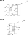
- FIG.1A shows a schematic cross-section view of a plug connector structure according to various embodiments in an unconnected state.
- FIG.1B shows a schematic cross-section view of a plug connector structure according to various embodiments in a connected state.
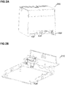
- FIG.2A shows a schematic perspective view of a printing device according to an embodiment.
- FIG.2B shows a schematic perspective view of a movable module for a printing device of FIG. 2A .
- FIG.3A and 3B show schematic perspective view of a plug connector structure of the embodiment of FIG.2A and 2B .
- each element of a list comprising a plurality of elements is also to be considered to be disclosed in combination with any further element of a further list.
- phrases "at least one of” with regard to a group of elements may be used herein to mean at least one element from the group consisting of the elements, i.e. the logical and/or.
- the phrase "at least one of” with regard to a group of elements may be used herein to mean a selection of: one of the listed elements, a plurality of one of the listed elements, a plurality of individual listed elements, or a plurality of a multiple of listed elements.
- Coupled is used herein to mean, for example, communicatively coupled, which may include type of a direct connection or an indirect connection. This may include any suitable wired connection and/or wireless connection.
- movable module is used herein to mean a structure, for example, a drawer, a hatch, a flap, a hub, an adapter, that is attached or attachable to a printer.
- the term "clearance” is used herein synonym to a play, a scope, a leeway, a wiggle room, a clearance or a similar term that refers to an engineering tolerance, e.g. a permissible limit or limit of variation, between a first and second body that are connected to each other. That is, the first and second body may some variation, e.g. in dimension or material composition that have some variation without significantly affecting the function of the assembly of the first and second body.
- FIG.1A shows a schematic cross-section view of a plug connector structure 100 according to various embodiments in an unconnected state
- FIG.1B shows a schematic cross-section view of a plug connector structure in a connected state.
- the plug connector structure 100 includes a plug 112 and a plug socket 104.
- the plug 112 is attached to a first board 110 and the plug socket 104 is attached to a second board 102.
- the plug 112 and plug socket 104 are configured correspondingly to form a plug connection 118 in case the plug 112 and the plug socket 104 are in close interlocking contact (illustrated in FIG.1B ).
- the present invention is not limited to this plug connection.
- Other types of plug connections are suitable too, e.g. a magnetic plug connection.
- the plug 112 is formed on the first board 110 and the plug socket 104 is formed on the second board 102.
- the present invention is not limited thereto, and the plug 112 may be formed on the second board 102 and the plug socket 104 may be formed on the first board 110 instead.
- One of the first and second boards 110, 102 comprises a plurality of pins 106 and the other of the first and second boards 110, 102 comprises a plurality of openings 114.
- Each opening 114 is configured to accommodate one pin 106, respectively.
- the pins 106 are configured such that the most distal end of the pins 106 are spaced apart farther than the most distal part of the plug 112 and plug socket 104 from the respective first or second board 102. Illustratively, as illustrated in FIG.1A , the pins protrude beyond the plug socket (or the plug - in a not illustrated alternative case).
- the openings 114 and pins 106 are configured such that a clearance 116 is formed between the opening 114 and the pin 106 respectively when the plug connection 118 is formed or established.
- the clearance 116 may be formed by an air gap.
- the openings 114 and pins 106 may have a circular cross-sectional shape, respectively.
- the openings 114 may have a first diameter and the pins 106 may have a second diameter.
- the second diameter may be smaller than the first diameter.
- a clearance also denoted e.g. as play, scope, leeway or wiggle room
- the clearance of the plug and plug socket is smaller than the clearance of the pins. This way, a blind accommodation of the plug in the plug socket is enabled.
- the pins 106 respectively include a tapered end 108 at a most distal end of the pins 106 from the board 102 to which the pins 106 are attached to (as illustrated in FIG.1A and 1B ).
- the tapered end of the pins 106 may be arranged circumferential to an end of a pin 106, respectively. This way, an accommodation of the pins in the openings is simplified.
- pins are formed on the second board 102 and openings 114 are formed on the first board 110.
- the present invention is not limited thereto, and pins may be formed on the first board 110 and openings 114 may be formed on the second board 110 instead.
- the first and second board 110, 102 each may include at least one pin 106 and at least each opening 114 each corresponding to the respective opening 114 and pin 106 of the other board.
- the first and/or second board 102 is a printed circuit board, respectively.
- at least one board is a printed circuit board and the other may be any other suitable planar carrier.
- the pins 106 and openings 114 form interlocking connections in directions radial to the respective extension directions of the pins 106.
- the plug 112 and the corresponding plug socket 104 are configured to establish a multiphase connection.
- the plug connection 118 may form an electrical connection or an optical connection.
- the plug 112 may be fixed to the first board 110 by a screw connection.
- the pins 106 may be formed integrally with the respective board. Alternatively, the pins 106 may be fixed to the respective board by a force-locking connection with the board, e.g. a rivet connection or a clamp-and-press connection.
- the openings 114 are formed as through holes in the respective board.
- the plug socket 104 is formed as a female connector strip and the plug 112 is formed as a male connector strip.
- the plurality of pins 106 includes an amount of pins 106 in the range of 2 to 6 pins, and the plurality of openings 114 includes the same amount of openings 114 as the amount of pins. This allows adjusting the clearance and simplifies the formation of the plug connection.
- the pluralities of openings 114 and pins 106 are arranged circumferential to the plug 112 or plug socket 104, respectively.
- the pins 106 are extended parallel or substantially parallel to the direction of the plug connection 118, as illustrated in Fig. 1A and 1B .
- the plug 112 and/or the plug socket 104 includes a tapered end at a most distal end from the first/second board 102 on which the plug 112/plug socket 104 is attached to.
- At least one of the first and second boards 110, 102 includes a further plug 300 or plug socket connected to the plug 112/plug socket 104 configured to be connected to the plug socket 104/plug 112 of the other of the first and second board 102, wherein the further plug 300 or plug socket is positioned on another side of the board, in particular an opposite side of the board, as illustrated in FIG. 3A .
- FIG.2A shows a schematic perspective view of a printing device 200 according to an embodiment.
- FIG.2B shows a schematic perspective view of a movable module 210 for a printing device 200 illustrated in FIG. 2A .
- FIG.3A and 3B show schematic perspective view of a plug connector structure of the embodiment of FIG.2A and 2B .
- the printing device 200 is configured to accommodate a movable module 210.
- Each of the printing device 200 and the movable module 210 include an accommodation structure 202, 204 configured to mechanically accommodate at least a part of the movable module 210 inside the printing device 200. Assembling the movable module 210 in the printing device 200 forms a printing device 200 having a movable module 210 (not illustrated).
- the accommodation structures 202, 204 have a clearance.
- the printing device 200 includes the first board 110 and the movable module 210 includes the second board 102, or vice versa, according to anyone of the aforementioned embodiments.
- the clearances 116 between the pins 106 and openings 114 are configured to counterbalance the clearance 116 of the accommodation structure.
- a counterbalance is established, as example, when the clearance of the pins is smaller than the clearance of the accommodation structures, and the clearance of the pins is smaller than the clearance of the plug and plug socket combined. This way, the plug connection is formed blindly while the movable module 210 and the printing device 200 are assembled.
- the clearance between the movable module and the printing device may be larger than the clearance between the openings and pins, respectively, and the clearance between the openings and pins may be larger than the clearance between the plug and plug socket and the pluralities of pins and openings introduce an intermediate level.
- the clearance may be reduced step-wise towards the most sensitive structure. This way, the most sensitive parts, e.g. the plug and plug socket, are not exposed to the relative large clearance of the movable module and printing device.
- the pluralities of pins and openings restrict the space of movement between the plug and plug socket and, thus, allow a blind assembling of plug and plug socket.
- the accommodation structures 202, 204 and the pins 106 may be separated parts.
- the printing device may be a printer, a copy machine, a fax machine or a plotter.
- the board of the movable module 210 includes a further plug 112 or plug socket connected to the plug 112/plug socket 104 configured to be connected to the plug socket 104/plug 112 of the board of the printing device, wherein the further plug 112 or plug socket 104 is exposed or exposable when the movable module 210 is accommodated in the printing device 200.
Landscapes
- Accessory Devices And Overall Control Thereof (AREA)
Abstract
Description
- Various embodiments relate generally to a plug connection structure, a movable module for a printing device, a printing device configured to accommodate a movable module and a printing device comprising the plug connection structure, respectively.
- In recent printing devices, powered universal serial bus (USB) sockets are attached to movable modules. As example, the movable module, e.g. a removable drawer, is accommodated inside the printing device. The USB socket of the movable module is connected to a circuit board of the printing device via a wired connection. The wired connection allows an electrical connection between the USB socket and the circuit board before the movable module is positioned in the final position in the printing device. This way, the electrical connection between the USB socket and the circuit board is established before the movable module is locked with the printing device. However, this way a relatively long wire is required. In addition, the accommodation of the movable module inside the printing device requires the manual steps of attaching the wire to the UBS socket and to the circuit board, and, further, the step of verifying that the wire is not obstructing the accommodation process of the removable module inside the printing device. As a consequence, customers spend a lot of time for the accommodation of the movable module inside the printing device.
- Therefore, in various embodiments, it may be provided a plug connection structure allowing a blind connection between a plug and a plug socket and, thus, a wired connection between the plug and plug socket is rendered optional or dispensable by the plug connection structure. Moreover, a movable module for a printing device, a printing device configured to accommodate a movable module and a printing device having a movable module may be provided each having a plug connection structure described before. This way, the process of assembling the movable module in the printing device may be simplified.
- In various embodiments, a plug connection structure may include a plug attached to a first board and a plug socket attached to a second board. The plug socket and the plug are configured correspondingly to form a plug connection. One of the first and second boards includes a plurality of pins and the other of the first and second boards includes a plurality of openings. The openings and pins are configured such that a clearance is formed between the opening and the pin respectively when the plug connection is formed. The clearance between the openings and pins is larger than the clearance between the plug and plug socket. The pins are configured such that the most distal end of the pins is spaced apart farther than the most distal part of the plug and plug socket from the respective first or second board.
- In various embodiments, a movable module for a printing device, a printing device configured to accommodate a movable module, and/or a printing device having a movable module are provided respectively, wherein each of the printing device and the movable module comprise an accommodation structure configured to mechanically accommodate at least a part of the movable module inside the printing device, wherein the assembly of the accommodation structures has a clearance. The printing device includes the first board and the movable module includes the second board, or vice versa, as mentioned above. The clearances between the pins and openings are configured to counterbalance the clearance of the accommodation structure.
- Further embodiments are described in the dependent claims and throughout the following specification.
- In the drawings, like reference characters generally refer to the same parts throughout the different views. The use of the same reference numbers in different figures indicates similar or identical items or features. The drawings are not necessarily to scale, emphasis instead generally being placed upon illustrating the principles of the invention. In the following description, various embodiments of the invention are described with reference to the following drawings, in which:
-
FIG.1A shows a schematic cross-section view of a plug connector structure according to various embodiments in an unconnected state. -
FIG.1B shows a schematic cross-section view of a plug connector structure according to various embodiments in a connected state. -
FIG.2A shows a schematic perspective view of a printing device according to an embodiment. -
FIG.2B shows a schematic perspective view of a movable module for a printing device ofFIG. 2A . -
FIG.3A and 3B show schematic perspective view of a plug connector structure of the embodiment ofFIG.2A and 2B . - The skilled in the art will recognize that the examples are not limited to the examples or drawings described. It should be understood that the drawings and detailed description thereto are not intended to limit examples to the particular form disclosed, but on the contrary, the intention is to cover all modifications, equivalents and alternatives falling within the spirit and scope as defined by the appended claims. As used throughout this application, the word "may" is used in a permissive sense (i.e., meaning having the potential to), rather than the mandatory sense (i.e., meaning must).
- Further, each element of a list comprising a plurality of elements is also to be considered to be disclosed in combination with any further element of a further list.
- The following detailed description refers to the accompanying drawings that show, by way of illustration, specific details and examples in which the invention may be practiced. These examples are described in sufficient detail to enable those skilled in the art to practice the invention. Other examples may be utilized and structural, logical, and electrical changes may be made without departing from the scope of the invention. The various examples are not necessarily mutually exclusive, as some examples can be combined with one or more other examples to form new examples. Various examples are described in connection with methods and various examples are described in connection with devices. However, it may be understood that examples described in connection with methods may similarly apply to the devices, and vice versa.
- The terms "at least one" and "one or more" may be understood to include any integer number greater than or equal to one, i.e. one, two, three, four, [...], etc. The term "a plurality" may be understood to include any integer number greater than or equal to two, i.e. two, three, four, five, [...], etc.
- The phrase "at least one of" with regard to a group of elements (for example at least one of A and B, or in the same way, at least one of A or B) may be used herein to mean at least one element from the group consisting of the elements, i.e. the logical and/or. For example, the phrase "at least one of" with regard to a group of elements may be used herein to mean a selection of: one of the listed elements, a plurality of one of the listed elements, a plurality of individual listed elements, or a plurality of a multiple of listed elements.
- The term "coupled" is used herein to mean, for example, communicatively coupled, which may include type of a direct connection or an indirect connection. This may include any suitable wired connection and/or wireless connection.
- The term "movable module" is used herein to mean a structure, for example, a drawer, a hatch, a flap, a hub, an adapter, that is attached or attachable to a printer.
- The term "clearance" is used herein synonym to a play, a scope, a leeway, a wiggle room, a clearance or a similar term that refers to an engineering tolerance, e.g. a permissible limit or limit of variation, between a first and second body that are connected to each other. That is, the first and second body may some variation, e.g. in dimension or material composition that have some variation without significantly affecting the function of the assembly of the first and second body.
-
FIG.1A shows a schematic cross-section view of aplug connector structure 100 according to various embodiments in an unconnected state andFIG.1B shows a schematic cross-section view of a plug connector structure in a connected state. - .The
plug connector structure 100 includes aplug 112 and aplug socket 104. Theplug 112 is attached to afirst board 110 and theplug socket 104 is attached to asecond board 102. Theplug 112 andplug socket 104 are configured correspondingly to form aplug connection 118 in case theplug 112 and theplug socket 104 are in close interlocking contact (illustrated inFIG.1B ). However, the present invention is not limited to this plug connection. Other types of plug connections are suitable too, e.g. a magnetic plug connection. - In
FIG. 1A and 1B , theplug 112 is formed on thefirst board 110 and theplug socket 104 is formed on thesecond board 102. However, the present invention is not limited thereto, and theplug 112 may be formed on thesecond board 102 and theplug socket 104 may be formed on thefirst board 110 instead. - One of the first and
second boards pins 106 and the other of the first andsecond boards openings 114. Eachopening 114 is configured to accommodate onepin 106, respectively. - The
pins 106 are configured such that the most distal end of thepins 106 are spaced apart farther than the most distal part of theplug 112 andplug socket 104 from the respective first orsecond board 102. Illustratively, as illustrated inFIG.1A , the pins protrude beyond the plug socket (or the plug - in a not illustrated alternative case). - The
openings 114 and pins 106 are configured such that aclearance 116 is formed between theopening 114 and thepin 106 respectively when theplug connection 118 is formed or established. As an example, theclearance 116 may be formed by an air gap. As an example, theopenings 114 and pins 106 may have a circular cross-sectional shape, respectively. Thus, theopenings 114 may have a first diameter and thepins 106 may have a second diameter. The second diameter may be smaller than the first diameter. This way, an air gap may be formed between a pin and the corresponding hole and, in addition, a clearance (also denoted e.g. as play, scope, leeway or wiggle room) is formed between a pin and the respective opening. The clearance of the plug and plug socket is smaller than the clearance of the pins. This way, a blind accommodation of the plug in the plug socket is enabled. - In various embodiments, the
pins 106 respectively include atapered end 108 at a most distal end of thepins 106 from theboard 102 to which thepins 106 are attached to (as illustrated inFIG.1A and 1B ). The tapered end of thepins 106 may be arranged circumferential to an end of apin 106, respectively. This way, an accommodation of the pins in the openings is simplified. - In
FIG. 1A and 1B , pins are formed on thesecond board 102 andopenings 114 are formed on thefirst board 110. However, the present invention is not limited thereto, and pins may be formed on thefirst board 110 andopenings 114 may be formed on thesecond board 110 instead. Alternatively, the first andsecond board pin 106 and at least each opening 114 each corresponding to therespective opening 114 and pin 106 of the other board. - In various embodiments, the first and/or
second board 102 is a printed circuit board, respectively. As example, at least one board is a printed circuit board and the other may be any other suitable planar carrier. - In various embodiments, the
pins 106 andopenings 114 form interlocking connections in directions radial to the respective extension directions of thepins 106. - In various embodiments, the
plug 112 and thecorresponding plug socket 104 are configured to establish a multiphase connection. As example, theplug connection 118 may form an electrical connection or an optical connection. - The
plug 112 may be fixed to thefirst board 110 by a screw connection. - The
pins 106 may be formed integrally with the respective board. Alternatively, thepins 106 may be fixed to the respective board by a force-locking connection with the board, e.g. a rivet connection or a clamp-and-press connection. - In various embodiments, the
openings 114 are formed as through holes in the respective board. - In various embodiments, the
plug socket 104 is formed as a female connector strip and theplug 112 is formed as a male connector strip. - In various embodiments, the plurality of
pins 106 includes an amount ofpins 106 in the range of 2 to 6 pins, and the plurality ofopenings 114 includes the same amount ofopenings 114 as the amount of pins. This allows adjusting the clearance and simplifies the formation of the plug connection. - In various embodiments, the pluralities of
openings 114 and pins 106 are arranged circumferential to theplug 112 or plugsocket 104, respectively. - In various embodiments, the
pins 106 are extended parallel or substantially parallel to the direction of theplug connection 118, as illustrated inFig. 1A and 1B . - In various embodiments, the
plug 112 and/or theplug socket 104 includes a tapered end at a most distal end from the first/second board 102 on which theplug 112/plug socket 104 is attached to. - In various embodiments, at least one of the first and
second boards further plug 300 or plug socket connected to theplug 112/plug socket 104 configured to be connected to theplug socket 104/plug 112 of the other of the first andsecond board 102, wherein thefurther plug 300 or plug socket is positioned on another side of the board, in particular an opposite side of the board, as illustrated inFIG. 3A . -
FIG.2A shows a schematic perspective view of aprinting device 200 according to an embodiment.FIG.2B shows a schematic perspective view of amovable module 210 for aprinting device 200 illustrated inFIG. 2A .FIG.3A and 3B show schematic perspective view of a plug connector structure of the embodiment ofFIG.2A and 2B . - The
printing device 200 is configured to accommodate amovable module 210. Each of theprinting device 200 and themovable module 210 include anaccommodation structure movable module 210 inside theprinting device 200. Assembling themovable module 210 in theprinting device 200 forms aprinting device 200 having a movable module 210 (not illustrated). Theaccommodation structures printing device 200 includes thefirst board 110 and themovable module 210 includes thesecond board 102, or vice versa, according to anyone of the aforementioned embodiments. Theclearances 116 between thepins 106 andopenings 114 are configured to counterbalance theclearance 116 of the accommodation structure. A counterbalance is established, as example, when the clearance of the pins is smaller than the clearance of the accommodation structures, and the clearance of the pins is smaller than the clearance of the plug and plug socket combined. This way, the plug connection is formed blindly while themovable module 210 and theprinting device 200 are assembled. - Illustratively, the clearance between the movable module and the printing device may be larger than the clearance between the openings and pins, respectively, and the clearance between the openings and pins may be larger than the clearance between the plug and plug socket and the pluralities of pins and openings introduce an intermediate level. In other words, the clearance may be reduced step-wise towards the most sensitive structure. This way, the most sensitive parts, e.g. the plug and plug socket, are not exposed to the relative large clearance of the movable module and printing device. In other words, the pluralities of pins and openings restrict the space of movement between the plug and plug socket and, thus, allow a blind assembling of plug and plug socket.
- The
accommodation structures pins 106 may be separated parts. - The printing device may be a printer, a copy machine, a fax machine or a plotter.
- The board of the
movable module 210 includes afurther plug 112 or plug socket connected to theplug 112/plug socket 104 configured to be connected to theplug socket 104/plug 112 of the board of the printing device, wherein thefurther plug 112 or plugsocket 104 is exposed or exposable when themovable module 210 is accommodated in theprinting device 200. - In the following, various examples are provided with reference to the Figures and embodiments described above.
- Example 1 is a plug connection structure, including a plug attached to a first board, and a plug socket attached to a second board. The plug socket and the plug are configured correspondingly to form a plug connection. One of the first and second boards includes a plurality of pins and the other of the first and second boards includes a plurality of openings. Each opening is configured to accommodate one pin, respectively, and the openings and pins are configured such that a clearance is formed between the opening and the pin respectively when the plug connection is formed. The clearance between the openings and pins is larger than the clearance between the plug and plug socket. The pins are configured such that the most distal end of the pins is spaced apart farther than the most distal part of the plug and plug socket from the respective first or second board. The clearance of the plug and plug socket is smaller than the clearance of the pins.
- In Example 2, the structure of Example 1 may optionally include that the first and/or second board is a printed circuit board, respectively.
- In Example 3, the structure of Example 1 or 2 may optionally include that the clearance is formed by an air gap.
- In Example 4, the structure of Example 1 to 3 may optionally include that the pins and openings form interlocking connections in directions radial to the respective extension directions of the pins.
- In Example 5, the structure of Example 1 to 4 may optionally include that the plug and the corresponding plug socket are configured to establish a multiphase connection.
- In Example 6, the structure of Example 1 to 5 may optionally include that the plug connection forms an electrical connection.
- In Example 7, the structure of Example 1 or 6 may optionally include that the plug connection forms an optical connection.
- In Example 8, the structure of Example 1 or 7 may optionally include that the plug is fixed to the first board by a screw connection.
- In Example 9, the structure of Example 1 to 8 may optionally include that the pins are formed integrally with the respective board.
- In Example 10, the structure of Example 1 to 9 may optionally include that the pins are fixed to the respective board by a force-locking connection with the board, in particular a rivet connection or a clamp-and-press connection.
- In Example 11, the structure of Example 1 to 10 may optionally include that the openings are formed as through holes in the respective board.
- In Example 12, the structure of Example 1 to 11 may optionally include that the plug socket is formed as a female connector strip and the plug is formed as a male connector strip.
- In Example 13, the structure of Example 1 to 12 may optionally include that the first and second board each includes at least one pin and at least each opening each corresponding to the respective opening and pin of the other board.
- In Example 14, the structure of Example 1 to 13 may optionally include that the plurality of pins includes an amount of pins in the range of 2 to 6 pins, and the plurality of openings includes the same amount of openings as the amount of pins.
- In Example 15, the structure of Example 1 to 14 may optionally include that the pluralities of openings and pins are arranged circumferential to the plug or plug socket, respectively.
- In Example 16, the structure of Example 1 to 15 may optionally include that the pins respectively include a tapered end at a most distal end of the pins from the board to which the pins are attached to.
- In Example 17, the structure of Example 16 may optionally include that the tapered end of the pins is circumferential to an end of a pin, respectively.
- In Example 18, the structure of Example 1 to 17 may optionally include that the pins are extended parallel or substantially parallel to the direction of the plug connection.
- In Example 19, the structure of Example 1 to 18 may optionally include that the openings have a first diameter and the pins have a second diameter, and wherein the second diameter is smaller than the first diameter.
- In Example 20, the structure of Example 1 to 19 may optionally include that the openings and pins have a circular cross-sectional shape, respectively.
- In Example 21, the structure of Example 1 to 20 may optionally include that the plug and/or the plug socket includes a tapered end at a most distal end from the first/second board on which the plug/plug socket is attached to.
- In Example 22, the structure of Example 1 to 21 may optionally include that at least one of the first and second boards includes a further plug or plug socket connected to the plug/plug socket configured to be connected to the plug socket/plug of the other of the first and second board, wherein the further plug or plug socket is positioned on another side of the board, in particular an opposite side of the board.
- Example 23 is a movable module for a printing device. Each of the printing device and the movable module include an accommodation structure configured to mechanically accommodate at least a part of the movable module inside the printing device. The assembly of the accommodation structures has a clearance. The printing device includes the first board and the movable module includes the second board, or vice versa, according to anyone of the aforementioned Examples 1 to 22. The clearances between the pins and openings are configured to counterbalance the clearance of the accommodation structure.
- Example 24 is a printing device configured to accommodate a movable module. Each of the printing device and the movable module include an accommodation structure configured to mechanically accommodate at least a part of the movable module inside the printing device. The assembly of the accommodation structures has a clearance. The printing device includes the first board and the movable module includes the second board, or vice versa, according to anyone of the aforementioned Examples 1 to 22. The clearances between the pins and openings are configured to counterbalance the clearance of the accommodation structure.
- Example 25 is a printing device having a movable module. Each of the printing device and the movable module include an accommodation structure configured to mechanically accommodate at least a part of the movable module inside the printing device. The assembly of the accommodation structures has a clearance. The printing device includes the first board and the movable module includes the second board, or vice versa, according to anyone of the aforementioned Examples 1 to 22. The clearances between the pins and openings are configured to counterbalance the clearance of the accommodation structure.
- In Example 26, the movable module and the printing device of Example 23 to 25 may optionally include that the accommodation structures and the pins are separated parts, respectively.
- In Example 27, the movable module and the printing device of Example 23 to 26 may optionally include that the printing device is a printer, a copy machine, a fax machine or a plotter.
- In Example 28, the movable module and the printing device of Example 23 to 25 may optionally include that the board of the movable module includes a further plug or plug socket connected to the plug/plug socket configured to be connected to the plug socket/plug of the board of the printing device, wherein the further plug or plug socket is exposed or exposable when the movable module is accommodated in the printing device.
- While the invention has been particularly shown and described with reference to specific examples, it should be understood by those skilled in the art that various changes in form and detail may be made therein without departing from the spirit and scope of the invention as defined by the appended claims. The scope of the invention is thus indicated by the appended claims and all changes which come within the meaning and range of equivalency of the claims are therefore intended to be embraced.
Claims (12)
- A plug connection structure (100), comprising
a plug (112) attached to a first board (110), and
a plug socket (104) attached to a second board (102), wherein the plug socket (104) and the plug (112) are configured correspondingly to form a plug connection (118), wherein one of the first and second boards (110, 102) comprises a plurality of pins (106) and the other of the first and second boards (110, 102) comprises a plurality of openings (114),
wherein each opening (114) is configured to accommodate one pin (106), respectively, and the openings (114) and pins (106) are configured such that a clearance (116) is formed between the opening (114) and the pin (106) respectively when the plug connection (118) is formed, wherein the clearance between the openings and pins is larger than the clearance between the plug and plug socket; and
wherein the pins (106) are configured such that the most distal end of the pins (106) is spaced apart farther than the most distal part of the plug (112) and plug socket (104) from the respective first or second board (102). - The plug connection structure (100) of claim 1,
wherein the pins (106) respectively comprise a tapered end (108) at a most distal end of the pins (106) from the board to which the pins (106) are attached to. - The plug connection structure (100) of claim 1 or 2,
wherein the pins (106) are extended parallel or substantially parallel to the direction of the plug connection (118). - The plug connection structure (100) of any one of claims 1 to 3,
wherein the openings (114) and pins (106) have a circular cross-sectional shape, respectively, and
the openings (114) have a first diameter and the pins (106) have a second diameter, and wherein the second diameter is smaller than the first diameter. - The plug connection structure (100) of any one of claims 1 to 4,
wherein the plug (112) and/or the plug socket (104) comprises a tapered end at a most distal end from the first/second board (102) on which the plug (112)/plug socket (104) is attached to. - The plug connection structure (100) of any one of claims 1 to 5,
wherein at least one of the first and second boards (110, 102) comprises a further plug (300) or plug socket connected to the plug (112)/plug socket (104) configured to be connected to the plug socket (104)/plug (112) of the other of the first and second board (102), wherein the further plug (300) or plug socket is positioned on another side of the board, in particular an opposite side of the board. - A movable module (210) for a printing device (200),
wherein each of the printing device (200) and the movable module (210) comprise an accommodation structure (202, 204) configured to mechanically accommodate at least a part of the movable module (210) inside the printing device (200), wherein the assembly of the accommodation structures (202, 204) has a clearance, and wherein the printing device (200) comprises the first board (110) and the movable module (210) comprises the second board (102), or vice versa, according to anyone of the aforementioned claims,
wherein the clearances between the pins (106) and openings (114) are configured to counterbalance the clearance of the accommodation structure (202, 204). - A printing device (200) configured to accommodate a movable module (210),
wherein each of the printing device (200) and the movable module (210) comprise an accommodation structure (202, 204) configured to mechanically accommodate at least a part of the movable module (210) inside the printing device (200), wherein the assembly of the accommodation structures (202, 204) has a clearance, and wherein the printing device (200) comprises the first board (110) and the movable module (210) comprises the second board (102), or vice versa, according to anyone of the claims 1 to 6,
wherein the clearances between the pins (106) and openings (114) are configured to counterbalance the clearance of the accommodation structure (202, 204). - A printing device (200) having a movable module (210),
wherein each of the printing device (200) and the movable module (210) comprise an accommodation structure (202, 204) configured to mechanically accommodate at least a part of the movable module (210) inside the printing device (200), wherein the assembly of the accommodation structures (202, 204) has a clearance, and wherein the printing device (200) comprises the first board (110) and the movable module (210) comprises the second board (102), or vice versa, according to anyone of the claims 1 to 6,
wherein the clearances between the pins (106) and openings (114) are configured to counterbalance the clearance of the accommodation structure (202, 204). - The printing device (200) and/or the movable module (210) according to anyone of claims 7 to 9,
wherein the accommodation structures (202, 204) and the pins (106) are separated parts. - The printing device (200) and/or movable module (210) according to anyone of claims 7 to 10, wherein the printing device (200) is a printer, a copy machine, a fax machine or a plotter.
- The printing device (200) and/or the movable module (210) according to anyone of claims 7 to 11,
wherein the board of the movable module (210) comprises a further plug (112) or plug socket (104) connected to the plug (112)/plug socket (104) configured to be connected to the plug socket (104)/plug (112) of the board of the printing device (200), wherein the further plug (112) or plug socket (104) is exposed or exposable when the movable module (210) is accommodated in the printing device (200).
Priority Applications (1)
| Application Number | Priority Date | Filing Date | Title |
|---|---|---|---|
| EP19154828.8A EP3691042A1 (en) | 2019-01-31 | 2019-01-31 | Plug connection structure, movable module for a printing device and printing device comprising the plug connection structure |
Applications Claiming Priority (1)
| Application Number | Priority Date | Filing Date | Title |
|---|---|---|---|
| EP19154828.8A EP3691042A1 (en) | 2019-01-31 | 2019-01-31 | Plug connection structure, movable module for a printing device and printing device comprising the plug connection structure |
Publications (1)
| Publication Number | Publication Date |
|---|---|
| EP3691042A1 true EP3691042A1 (en) | 2020-08-05 |
Family
ID=65276037
Family Applications (1)
| Application Number | Title | Priority Date | Filing Date |
|---|---|---|---|
| EP19154828.8A Pending EP3691042A1 (en) | 2019-01-31 | 2019-01-31 | Plug connection structure, movable module for a printing device and printing device comprising the plug connection structure |
Country Status (1)
| Country | Link |
|---|---|
| EP (1) | EP3691042A1 (en) |
Citations (6)
| Publication number | Priority date | Publication date | Assignee | Title |
|---|---|---|---|---|
| US4998892A (en) * | 1990-03-12 | 1991-03-12 | Itt Corporation | Guide pin apparatus for module connector |
| US5391091A (en) * | 1993-06-30 | 1995-02-21 | American Nucleonics Corporation | Connection system for blind mate electrical connector applications |
| US20040216318A1 (en) * | 2003-04-30 | 2004-11-04 | Sun Microsystems, Inc. | Alignment device and method of connecting a circuit card to a mid plane |
| US7404726B1 (en) * | 2008-01-31 | 2008-07-29 | International Business Machines Corporation (Ibm) | Apparatus and method for floating connector capture |
| US20100118497A1 (en) * | 2008-11-10 | 2010-05-13 | Fujitsu Limited | Module structure |
| CN101783460A (en) * | 2010-03-01 | 2010-07-21 | 李立国 | Vibration isolation device of blind-mate connector of power battery box of electric vehicle |
-
2019
- 2019-01-31 EP EP19154828.8A patent/EP3691042A1/en active Pending
Patent Citations (6)
| Publication number | Priority date | Publication date | Assignee | Title |
|---|---|---|---|---|
| US4998892A (en) * | 1990-03-12 | 1991-03-12 | Itt Corporation | Guide pin apparatus for module connector |
| US5391091A (en) * | 1993-06-30 | 1995-02-21 | American Nucleonics Corporation | Connection system for blind mate electrical connector applications |
| US20040216318A1 (en) * | 2003-04-30 | 2004-11-04 | Sun Microsystems, Inc. | Alignment device and method of connecting a circuit card to a mid plane |
| US7404726B1 (en) * | 2008-01-31 | 2008-07-29 | International Business Machines Corporation (Ibm) | Apparatus and method for floating connector capture |
| US20100118497A1 (en) * | 2008-11-10 | 2010-05-13 | Fujitsu Limited | Module structure |
| CN101783460A (en) * | 2010-03-01 | 2010-07-21 | 李立国 | Vibration isolation device of blind-mate connector of power battery box of electric vehicle |
Similar Documents
| Publication | Publication Date | Title |
|---|---|---|
| CA2328231C (en) | Circuit card insertion and removal system | |
| US5137462A (en) | Adapter for stacking connector assembly | |
| US6435889B1 (en) | Reduced complexity hot plug blind mate fan assembly and connector therefor | |
| EP1453151A2 (en) | Housing for jack assembly | |
| EP0485196A2 (en) | Optical connection to backplanes | |
| JP2000148214A (en) | Programmable logic controller and programmable logic controller module | |
| CN108011231B (en) | Board connector | |
| US20160294081A1 (en) | Configurable guide hardware for connector systems | |
| US7163424B2 (en) | Housing for a thin active probe | |
| CN112787171A (en) | Base connector | |
| EP1345290A1 (en) | Apparatus and Method for Electrical Connector Cable Retention | |
| US7182608B2 (en) | Chessboard electrical connector | |
| EP1903649A2 (en) | Electric wire holding device and television receiver provided with the same | |
| US9516780B2 (en) | Device for accommodating mounting rail module cases | |
| TWI736764B (en) | Wiring transposing adapter | |
| JP2008535466A (en) | Module rear wall for switchgear assembly module, switchgear assembly module, and electrical switchgear assembly | |
| US6667887B2 (en) | Method and apparatus for locating and securing a component in a computer system | |
| US11183790B2 (en) | Connector housing and electrical connector | |
| EP4586416A2 (en) | Connector disengage resistance mechanism | |
| CN219760000U (en) | Connector with a plurality of connectors | |
| CN102332661A (en) | Alignment pins to hold the module on the board | |
| US20140154898A1 (en) | Electrical center and connector assembly system | |
| JP6607222B2 (en) | Connection auxiliary member and grommet | |
| CN117296459A (en) | Modular electronic assembly | |
| TWI791015B (en) | Receptacle frames for adapting a float range capability of a blind-mate connector and related systems |
Legal Events
| Date | Code | Title | Description |
|---|---|---|---|
| PUAI | Public reference made under article 153(3) epc to a published international application that has entered the european phase |
Free format text: ORIGINAL CODE: 0009012 |
|
| STAA | Information on the status of an ep patent application or granted ep patent |
Free format text: STATUS: THE APPLICATION HAS BEEN PUBLISHED |
|
| AK | Designated contracting states |
Kind code of ref document: A1 Designated state(s): AL AT BE BG CH CY CZ DE DK EE ES FI FR GB GR HR HU IE IS IT LI LT LU LV MC MK MT NL NO PL PT RO RS SE SI SK SM TR |
|
| AX | Request for extension of the european patent |
Extension state: BA ME |
|
| STAA | Information on the status of an ep patent application or granted ep patent |
Free format text: STATUS: REQUEST FOR EXAMINATION WAS MADE |
|
| 17P | Request for examination filed |
Effective date: 20210126 |
|
| RBV | Designated contracting states (corrected) |
Designated state(s): AL AT BE BG CH CY CZ DE DK EE ES FI FR GB GR HR HU IE IS IT LI LT LU LV MC MK MT NL NO PL PT RO RS SE SI SK SM TR |
|
| STAA | Information on the status of an ep patent application or granted ep patent |
Free format text: STATUS: EXAMINATION IS IN PROGRESS |
|
| 17Q | First examination report despatched |
Effective date: 20211129 |
|
| RAP1 | Party data changed (applicant data changed or rights of an application transferred) |
Owner name: DIEBOLD NIXDORF SYSTEMS GMBH |