EP3690940A1 - Tiled display device - Google Patents
Tiled display device Download PDFInfo
- Publication number
- EP3690940A1 EP3690940A1 EP20150183.0A EP20150183A EP3690940A1 EP 3690940 A1 EP3690940 A1 EP 3690940A1 EP 20150183 A EP20150183 A EP 20150183A EP 3690940 A1 EP3690940 A1 EP 3690940A1
- Authority
- EP
- European Patent Office
- Prior art keywords
- substrate
- light
- pixel
- emitting unit
- edge
- Prior art date
- Legal status (The legal status is an assumption and is not a legal conclusion. Google has not performed a legal analysis and makes no representation as to the accuracy of the status listed.)
- Granted
Links
Images




Classifications
-
- H—ELECTRICITY
- H10—SEMICONDUCTOR DEVICES; ELECTRIC SOLID-STATE DEVICES NOT OTHERWISE PROVIDED FOR
- H10W—GENERIC PACKAGES, INTERCONNECTIONS, CONNECTORS OR OTHER CONSTRUCTIONAL DETAILS OF DEVICES COVERED BY CLASS H10
- H10W90/00—Package configurations
-
- G—PHYSICS
- G09—EDUCATION; CRYPTOGRAPHY; DISPLAY; ADVERTISING; SEALS
- G09F—DISPLAYING; ADVERTISING; SIGNS; LABELS OR NAME-PLATES; SEALS
- G09F9/00—Indicating arrangements for variable information in which the information is built-up on a support by selection or combination of individual elements
- G09F9/30—Indicating arrangements for variable information in which the information is built-up on a support by selection or combination of individual elements in which the desired character or characters are formed by combining individual elements
- G09F9/302—Indicating arrangements for variable information in which the information is built-up on a support by selection or combination of individual elements in which the desired character or characters are formed by combining individual elements characterised by the form or geometrical disposition of the individual elements
- G09F9/3026—Video wall, i.e. stackable semiconductor matrix display modules
-
- G—PHYSICS
- G09—EDUCATION; CRYPTOGRAPHY; DISPLAY; ADVERTISING; SEALS
- G09G—ARRANGEMENTS OR CIRCUITS FOR CONTROL OF INDICATING DEVICES USING STATIC MEANS TO PRESENT VARIABLE INFORMATION
- G09G3/00—Control arrangements or circuits, of interest only in connection with visual indicators other than cathode-ray tubes
- G09G3/20—Control arrangements or circuits, of interest only in connection with visual indicators other than cathode-ray tubes for presentation of an assembly of a number of characters, e.g. a page, by composing the assembly by combination of individual elements arranged in a matrix no fixed position being assigned to or needed to be assigned to the individual characters or partial characters
- G09G3/22—Control arrangements or circuits, of interest only in connection with visual indicators other than cathode-ray tubes for presentation of an assembly of a number of characters, e.g. a page, by composing the assembly by combination of individual elements arranged in a matrix no fixed position being assigned to or needed to be assigned to the individual characters or partial characters using controlled light sources
- G09G3/30—Control arrangements or circuits, of interest only in connection with visual indicators other than cathode-ray tubes for presentation of an assembly of a number of characters, e.g. a page, by composing the assembly by combination of individual elements arranged in a matrix no fixed position being assigned to or needed to be assigned to the individual characters or partial characters using controlled light sources using electroluminescent panels
- G09G3/32—Control arrangements or circuits, of interest only in connection with visual indicators other than cathode-ray tubes for presentation of an assembly of a number of characters, e.g. a page, by composing the assembly by combination of individual elements arranged in a matrix no fixed position being assigned to or needed to be assigned to the individual characters or partial characters using controlled light sources using electroluminescent panels semiconductive, e.g. using light-emitting diodes [LED]
-
- H—ELECTRICITY
- H10—SEMICONDUCTOR DEVICES; ELECTRIC SOLID-STATE DEVICES NOT OTHERWISE PROVIDED FOR
- H10H—INORGANIC LIGHT-EMITTING SEMICONDUCTOR DEVICES HAVING POTENTIAL BARRIERS
- H10H20/00—Individual inorganic light-emitting semiconductor devices having potential barriers, e.g. light-emitting diodes [LED]
- H10H20/80—Constructional details
- H10H20/85—Packages
- H10H20/857—Interconnections, e.g. lead-frames, bond wires or solder balls
-
- H—ELECTRICITY
- H10—SEMICONDUCTOR DEVICES; ELECTRIC SOLID-STATE DEVICES NOT OTHERWISE PROVIDED FOR
- H10W—GENERIC PACKAGES, INTERCONNECTIONS, CONNECTORS OR OTHER CONSTRUCTIONAL DETAILS OF DEVICES COVERED BY CLASS H10
- H10W70/00—Package substrates; Interposers; Redistribution layers [RDL]
- H10W70/60—Insulating or insulated package substrates; Interposers; Redistribution layers
- H10W70/67—Insulating or insulated package substrates; Interposers; Redistribution layers characterised by their insulating layers or insulating parts
- H10W70/688—Flexible insulating substrates
-
- H—ELECTRICITY
- H05—ELECTRIC TECHNIQUES NOT OTHERWISE PROVIDED FOR
- H05K—PRINTED CIRCUITS; CASINGS OR CONSTRUCTIONAL DETAILS OF ELECTRIC APPARATUS; MANUFACTURE OF ASSEMBLAGES OF ELECTRICAL COMPONENTS
- H05K1/00—Printed circuits
- H05K1/18—Printed circuits structurally associated with non-printed electric components
- H05K1/189—Printed circuits structurally associated with non-printed electric components characterised by the use of flexible or folded printed circuits
-
- H—ELECTRICITY
- H05—ELECTRIC TECHNIQUES NOT OTHERWISE PROVIDED FOR
- H05K—PRINTED CIRCUITS; CASINGS OR CONSTRUCTIONAL DETAILS OF ELECTRIC APPARATUS; MANUFACTURE OF ASSEMBLAGES OF ELECTRICAL COMPONENTS
- H05K2201/00—Indexing scheme relating to printed circuits covered by H05K1/00
- H05K2201/05—Flexible printed circuits [FPCs]
- H05K2201/056—Folded around rigid support or component
-
- H—ELECTRICITY
- H05—ELECTRIC TECHNIQUES NOT OTHERWISE PROVIDED FOR
- H05K—PRINTED CIRCUITS; CASINGS OR CONSTRUCTIONAL DETAILS OF ELECTRIC APPARATUS; MANUFACTURE OF ASSEMBLAGES OF ELECTRICAL COMPONENTS
- H05K2201/00—Indexing scheme relating to printed circuits covered by H05K1/00
- H05K2201/10—Details of components or other objects attached to or integrated in a printed circuit board
- H05K2201/10007—Types of components
- H05K2201/10106—Light emitting diode [LED]
-
- H—ELECTRICITY
- H05—ELECTRIC TECHNIQUES NOT OTHERWISE PROVIDED FOR
- H05K—PRINTED CIRCUITS; CASINGS OR CONSTRUCTIONAL DETAILS OF ELECTRIC APPARATUS; MANUFACTURE OF ASSEMBLAGES OF ELECTRICAL COMPONENTS
- H05K2201/00—Indexing scheme relating to printed circuits covered by H05K1/00
- H05K2201/10—Details of components or other objects attached to or integrated in a printed circuit board
- H05K2201/10007—Types of components
- H05K2201/10128—Display
-
- Y—GENERAL TAGGING OF NEW TECHNOLOGICAL DEVELOPMENTS; GENERAL TAGGING OF CROSS-SECTIONAL TECHNOLOGIES SPANNING OVER SEVERAL SECTIONS OF THE IPC; TECHNICAL SUBJECTS COVERED BY FORMER USPC CROSS-REFERENCE ART COLLECTIONS [XRACs] AND DIGESTS
- Y02—TECHNOLOGIES OR APPLICATIONS FOR MITIGATION OR ADAPTATION AGAINST CLIMATE CHANGE
- Y02E—REDUCTION OF GREENHOUSE GAS [GHG] EMISSIONS, RELATED TO ENERGY GENERATION, TRANSMISSION OR DISTRIBUTION
- Y02E10/00—Energy generation through renewable energy sources
- Y02E10/50—Photovoltaic [PV] energy
- Y02E10/549—Organic PV cells
Definitions
- the present disclosure relates to a tiled display device, and in particular it relates to a tiled display device having a better connection space.
- Mini light-emitting diode technology is a flat panel display technology that has emerged in recent years. Mini light-emitting diode display devices can produce seamless images with wide viewing angles, high brightness, and high contrast. However, when mini light-emitting diode technology is applied to a large-sized display panel, most of them need to be tiled together to achieve a display function. As the requirements for resolution increase, the pitch between the mini light-emitting diodes decreases, which also limits the available space at the connection position of the panel.
- tiled display devices Although currently existing tiled display devices have been adequate for their intended purposes, they have not been satisfactory in all respects. Therefore, the development of the structural design that can improve the quality or reliability of tiled display devices is still one of the goals that the industry is currently aiming at.
- a tiled display device includes a first substrate, a second substrate and a light-emitting unit.
- the first substrate includes a first main substrate and a first flexible substrate.
- the first flexible substrate is disposed on the first main substrate.
- the second substrate is disposed adjacent to the first substrate.
- the light-emitting unit is disposed on the first flexible substrate. In addition, a portion of the light-emitting unit protrudes from an edge of the first main substrate.
- a first material layer is disposed on or over a second material layer may indicate that the first material layer is in direct contact with the second material layer, or that the first material layer is not in direct contact with the second material layer, there being one or more intermediate layers disposed between the first material layer and the second material layer.
- terms concerning attachments, coupling and the like such as “connected” and “interconnected”, refer to a relationship wherein structures are secured or attached to one another either directly or indirectly through intervening structures, as well as both movable or rigid attachments or relationships, unless expressly described otherwise.
- the bendable area of the flexible substrate may be increased by the design of the connection pad or the packaging structure of the light-emitting unit. Accordingly, the risk of disconnection of wirings at the bending portion of the flexible substrate may be reduced, or the impact on the panel resolution at the connection positions of the panels may be reduced.
- FIG. 1A is a top-view diagram of a tiled display device 10A in accordance with some embodiments of the present disclosure. It should be understood that FIG. 1A only illustrates some components of the tiled display device 10A for clarity. In addition, additional features may be added to the tiled display device 10A described below in accordance with some embodiments. In accordance with some other embodiments, some of the features of the tiled display device 10A may be replaced or omitted.
- the tiled display device 10A may include a liquid-crystal display (LCD), a light-emitting diode (LED), a quantum dot, fluorescence, and phosphor, other suitable display media, or a combination thereof, but it is not limited thereto.
- the light-emitting diode display device may include, for example, an organic light-emitting diode (OLED), a quantum dot light-emitting diode (QLED), and a mini light-emitting diode (mini LED), or a micro light-emitting diode (micro LED), but it is not limited thereto.
- OLED organic light-emitting diode
- QLED quantum dot light-emitting diode
- mini LED mini light-emitting diode
- micro LED micro light-emitting diode
- the tiled display device 10A may include a first substrate 100 and a second substrate 200, and the second substrate 200 may be disposed adjacent to the first substrate 100.
- the first substrate 100 may include a main region 100m, an edge region 100e, and an extension region 100ex.
- the edge region 100e connects between the main region 100m and the extension region 100ex.
- the second substrate 200 may include a main region 200m, an edge region 200e, and an extension region 200ex.
- the edge region 200e connects between the main region 200m and the extension region 200ex.
- the edge region 100e and the edge region 200e are adjacent to each other.
- the edge region 100e and the edge region 200e may be used as a bendable region or a region where the first substrate 100 and the second substrate 200 are connected.
- the extension region 100ex and the extension region 200ex may be bent below the first substrate 100 and the second substrate 200.
- the definitions of the extension region 100ex, the extension region 200ex, the edge region 100e, the edge region 200e, the main region 100m, and the main region 200m will be further explained in FIG. 1B .
- the tiled display device 10A may include a plurality of light-emitting units 300, and the light-emitting units 300 may be disposed on the first substrate 100 and the second substrate 200.
- a portion of the light-emitting unit 300 may overlap with the main region 100m or the main region 200m and may not overlap with the edge region 100e or the edge region 200e; and a portion of the light-emitting unit 300 may partially overlap with the main region 100m or the main region 200m and may partially overlap with the edge region 100e of the first substrate 100 or the edge region 200e of the second substrate 200.
- one light-emitting unit 300 may include or correspond to one pixel 301, but the present disclosure is not limited thereto. In accordance with some embodiments, one light-emitting unit 300 may include or correspond to a plurality of pixels 301. In addition, the pixel 301 may include one or more subpixels. As shown in FIG. 1A , in some embodiments, one light-emitting unit 300 may include one pixel 301, and the pixel 301 may include, for example, three sub-pixels, i.e. sub-pixel 301a, sub-pixel 301b, and sub-pixel 301c.
- the sub-pixel 301a, sub-pixel 301b, and sub-pixel 301c may be red, green, and blue sub-pixels that are arranged in a suitable manner, but the present disclosure is not limited thereto.
- one pixel 301 may include red, green, blue, or white sub-pixels, or sub-pixels having other suitable colors, but the present disclosure is not limited thereto.
- the sub-pixel 301a, sub-pixel 301b, and sub-pixel 301c may be the dies of light-emitting diodes that emit light of different colors, or the dies of light-emitting diode that emit light of the same color.
- a pitch P 1 may exist between two pixels 301.
- the term “pitch” may refer to a distance between an edge (e.g., the left-side edge) of a subpixel (e.g., sub-pixel 301a) and the same side edge (e.g., the left-side edge) of the next or the nearest same type subpixel (e.g., another sub-pixel 301a).
- the "pitch” described above may be defined by sub-pixels that emit light of the same color.
- the "light of the same color” means that a wavelength difference between the maximum peaks in the spectra of the two light sources is between -5 nm to 5nm, but the present disclosure is not limited thereto. As shown in FIG.
- the light-emitting unit 300 may include one pixel 301, and the pixel 301 may include three sub-pixels.
- the "pitch" described above may be, for example, a distance between the left-side edge of a sub-pixel (e.g., sub-pixel 301a) in one light-emitting unit 300 and the left-side edge of the same type sub-pixel (e.g., another sub-pixel 301a) in another adjacent light-emitting unit 300.
- the light-emitting unit 300 may include a plurality of connection pads 303.
- the connection pads 303 may be disposed on the first substrate 100 and the second substrate 200, and the connection pads 303 may be disposed between the pixel 301 and first substrate 100, or between the pixel 301 and the second substrate 200.
- the connection pad 303 may provide electrical connection between the light-emitting unit 300 and the first substrate 100 and the second substrate 200.
- a layout layer (not illustrated) of various wirings or electronic circuits may be disposed on the edge region 100e of the first substrate 100 or the edge region 200e of the second substrate 200, or the front surfaces (e.g., the extension region 100ex or the extension region 200ex) or the rear surfaces (e.g., the main region 100m or the main region 200m) of the first substrate 100 and the second substrate 200.
- the layout layer (not illustrated) may be electrically connected to the light-emitting unit 300 through the connection pads 303.
- the first substrate 100 and the second substrate 200 are drawn separately. That is, the state before the first substrate 100 and the second substrate 200 are tiled (joined) is illustrated.
- the tiled display device 10A may include any suitable amount of the substrates as needed in accordance with some embodiments, but the present disclosure is not limited thereto.
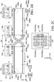
- FIG. 1B is an enlarged cross-sectional diagram of the edge region 100e, the edge region 200e, the extension region 100ex and extension region 200ex in the region A in FIG. 1A after the first substrate 100 and the second substrate 200 are tiled (joined) in accordance with some embodiments of the present disclosure.
- the structure of the tiled display device 10A at the connection position is further explained as follows.
- the first substrate 100 may include a first main substrate 100a and a first flexible substrate 100b, and the first flexible substrate 100b may be disposed on the first main substrate 100a.
- the second substrate 200 may include a second main substrate 200a and a second flexible substrate 200b, and the second flexible substrate 200b may be disposed on the second main substrate 200a.
- the first main substrate 100a may have an upper surface 100at, a lower surface 100ab, and an edge 100as.
- the first flexible substrate 100b may extend from the upper surface 100at to the lower surface 100ab.
- the first flexible substrate 100b may be optionally not in contact with the edge 100as.
- the second main substrate 200a may have an upper surface 200at, a lower surface 200ab, and an edge 200as.
- the second flexible substrate 200b may extend from the upper surface 200at to the lower surface 200ab. In some embodiments, the second flexible substrate 200b may not be in contact with the edge 200as.
- the first main substrate 100a and the second main substrate 200a may be a flexible substrate, a rigid substrate, or a combination thereof.
- the material of the first main substrate 100a and the second main substrate 200a may include, but is not limited to, glass, quartz, sapphire, ceramic, plastic, other suitable substrate materials, or a combination thereof.
- the material of the plastic substrate may include, but is not limited to, polyimide (PI), polyethylene terephthalate (PET), polycarbonate (PC), other suitable materials, or a combination thereof.
- the material of the glass substrate may include, but is not limited to, silicon (Si), silicon carbide (SiC), gallium nitride (GaN), silicon dioxide (SiO 2 ), other suitable materials, or a combination thereof.
- the first main substrate 100a and the second main substrate 200a may include a metal-glass fiber composite plate or a metal-ceramic composite plate, but they are not limited thereto.
- the material of the first main substrate 100a may be the same as or different from the material of the second main substrate 200a.
- the first flexible substrate 100b and the second flexible substrate 200b may include a material having flexible characteristics.
- the material of the first flexible substrate 100b and the second flexible substrate 200b may include, but is not limited to, polyimide (PI), polyethylene terephthalate (PET), polycarbonate (PC), other suitable materials, or a combination thereof.
- the material of the first flexible substrate 100b may be the same as or different from the material of the second flexible substrate 200b.
- the first substrate 100 may include the main region 100m, the extension region 100ex, and the edge region 100e.
- the main region 100m is the region of the first flexible substrate 100b that is adjacent to the upper surface 100at of the first main substrate 100a and overlaps the upper surface 100at of the first main substrate 100a in the normal direction of the first main substrate 100a (e.g., the Z direction shown in the figure).
- the extension region 100ex is the region of first flexible substrate 100b that is adjacent to the lower surface 100ab of the first main substrate 100a and overlaps the lower surface 100ab of the first main substrate 100a in the normal direction of the first main substrate 100a.
- the edge region 100e is the region of the first flexible substrate 100b excluding the main region 100m and the extension region 100ex.
- the second substrate 200 may include the main region 200m, the extension region 200ex, and the edge region 200e.
- the main region 200m is the region of the second flexible substrate 200b that is adjacent to the upper surface 200at of the second main substrate 200a and overlaps the upper surface 200at of the second main substrate 200a in the normal direction of the second main substrate 200a (e.g., the Z direction shown in the figure).
- the extension region 200ex is the region of the second flexible substrate 200b that is adjacent to the lower surface 200ab of the second main substrate 200a and overlaps the lower surface 200ab of the second main substrate 200a in the normal direction of the second main substrate 200a.
- the edge region 200e is the region of the second flexible substrate 200b excluding the main region 200m and the extension region 200ex.
- the light-emitting units 300 may be disposed on the first flexible substrate 100b, and a portion of the light-emitting unit 300 may overlap the upper surface 100at, and another portion of the light-emitting unit 300 may protrude from the upper surface 100at or the edge 100as of the first main substrate 100a. In other words, in some embodiments, a portion of the light-emitting units 300 may overlap the edge region 100e in the normal direction of the first main substrate 100a.
- the light-emitting unit 300 may also be disposed on the second flexible substrate 200b, and a portion of the light-emitting unit 300 may overlap the upper surface 200at, and another portion of the light-emitting unit 300 may protrude from the upper surface 200at or the edge 200as of the second main substrate 200a. In other words, in some embodiments, a portion of the light-emitting unit 300 may overlap the edge region 200e in the normal direction of the second main substrate 200a.
- the first flexible substrate 100b may be disposed between the first substrate 100 and the second substrate 200. Specifically, in some embodiments, at least a portion of the first flexible substrate 100b may be disposed between the edge 100as of the first main substrate 100a and the edge 200as of the second main substrate 200a. In some embodiments, in the normal direction of the first main substrate 100a or the second main substrate 200a (e.g., the Z direction shown in the figure), a portion of the light-emitting unit 300 may overlap the first flexible substrate 100b that is disposed between the edge 100as and the edge 200as.
- the second flexible substrate 200b may be disposed between the first substrate 100 and the second substrate 200, for example, between the edge 100as of the first main substrate 100a and the edge 200as of the second main substrate 200a.
- the light-emitting unit 300 may include one or more pixels 301, and the pixel 301 may include a suitable number of sub-pixels, such as sub-pixel 301a, sub-pixel 301b, and sub-pixel 310c.
- the light-emitting unit 300 may include one pixel 301, and the pixel 301 may include three sub-pixels.
- the sub-pixel 301a, the sub-pixel 301b, and the sub-pixel 310c are three dies of the light-emitting diodes.
- the light-emitting unit 300 may include a plurality of connection pads 303, and the connection pads 303 may be disposed on the first flexible substrate 100b and the second flexible substrate 200b.
- the first flexible substrate 100b and the second flexible substrate 200b may include a layout layer (not illustrated) of various wirings or electronic circuits disposed thereon, and the layout layer (not illustrated) may be electrically connected to the light-emitting units 300 through the connection pads 303.
- connection pad 303 may be electrically connected to an anode electrode or a cathode electrode of the die of the light-emitting unit 300.
- the light-emitting unit 300 has three sub-pixels, i.e. sub-pixel 301a, sub-pixel 301b, and sub-pixel 310c.
- the three connection pads 303 may be electrically connected to the anode electrodes of the dies of the sub-pixel 301a, sub-pixel 301b, and sub-pixel 310c, and one connection pad 303 may be electrically connected to the cathode electrode of the dies of the sub-pixel 301a, sub-pixel 301b, and sub-pixel 310c. That is, the three sub-pixels 301a, 301b, and 310c may have a common cathode, but the manner of polarity connection is not limited thereto.
- connection pad 303 may include a conductive material.
- the connection pad 303 may include a metal conductive material, a transparent conductive material, or a combination thereof.
- the metal conductive material may include, but is not limited to, copper (Cu), aluminum (Al), molybdenum (Mo), silver (Ag), tin (Sn), tungsten (W), gold (Au), chromium (Cr), nickel (Ni), platinum (Pt), copper alloy, aluminum alloy, molybdenum alloy, silver alloy, tin alloy, tungsten alloy, gold alloy, chromium alloy, nickel alloy, platinum alloy, other suitable metal materials, or a combination thereof.
- the transparent conductive material may include a transparent conductive oxide (TCO).
- TCO transparent conductive oxide
- the transparent conductive oxide may include, but is not limited to, indium tin oxide (ITO), tin oxide (SnO), zinc oxide (ZnO), indium zinc oxide (IZO), indium gallium zinc oxide (IGZO), indium tin zinc oxide (ITZO), antimony tin oxide (ATO), antimony zinc oxide (AZO), other suitable transparent conductive materials, or a combination thereof.
- a chemical vapor deposition (CVD) process may be used to form the connection pad 303, but the present disclosure is not limited thereto.
- CVD chemical vapor deposition
- PVD physical vapor deposition
- electroplating process an electroless plating process, other suitable processes, or a combination thereof
- other suitable processes or a combination thereof
- the light-emitting unit 300 may further include an intermediate substrate 305 disposed between the pixel 301 and the connection pad 303, and a protective layer 307 disposed above the intermediate substrate 305.
- the pixel 301 may be electrically connected to the connection pad 303 through a via (not illustrated) that penetrates through the intermediate substrate 305, but it is not limited thereto.
- the protective layer 307 may optionally cover the top surface and the side surface of the pixel 301.
- the intermediate substrate 305 may be a flexible substrate, a rigid substrate, or a combination thereof.
- the intermediate substrate 305 may include, but is not limited to, a glass substrate, a ceramic substrate, a plastic substrate, other suitable substrate materials, or a combination thereof.
- the material of the intermediate substrate 305 may include, but is not limited to, epoxy resins, polymerized siloxanes (silicone), polyimide (PI), and polyethylene terephthalate (PET), polycarbonate (PC), other suitable materials, or a combination thereof.
- the material of the glass substrate may include, but is not limited to, silicon (Si), silicon carbide (SiC), gallium nitride (GaN), silicon dioxide (SiO 2 ), other suitable materials, or a combination thereof.
- the intermediate substrate 305 may include a printed circuit board (PCB), a metal-glass fiber composite plate, or a metal-ceramic composite plate, but it is not limited thereto.
- the protective layer 307 may include, but is not limited to, organic materials, inorganic materials, other suitable packaging materials, or a combination thereof.
- the inorganic material may include, but is not limited to, silicon nitride, silicon oxide, silicon oxynitride, aluminum oxide, or other suitable materials.
- the organic material may include, but is not limited to, epoxy resins, silicone resins, acrylic resins (such as polymethylmetacrylate (PMMA), benzocyclobutene (BCB), polyimide, polyester, polydimethylsiloxane (PDMS), tetrafluoroethylene-perfluoroalkoxy vinyl ether copolymer (polyfluoroalkoxy, PFA), other suitable materials, or a combination thereof.
- epoxy resins such as polymethylmetacrylate (PMMA), benzocyclobutene (BCB), polyimide, polyester, polydimethylsiloxane (PDMS), tetrafluoroethylene-perfluoroalkoxy vinyl ether copolymer (polyfluoroalkoxy, PFA), other suitable materials, or a combination thereof.
- silicone resins such as polymethylmetacrylate (PMMA), benzocyclobutene (BCB), polyimide, polyester, polydimethylsiloxane (PDMS), tetraflu
- the protective layer 307 may have a function of wavelength conversion, for example, a light source generated by the pixel 301 may be converted into light having a specific wavelength range (specific color).
- the protective layer 307 may further include particles having a wavelength conversion function, such as phosphors, quantum dot (QD) materials, organic fluorescent materials, other suitable materials, or a combination thereof, but it is not limited thereto.
- the protective layer 307 may be formed by the chemical vapor deposition process, a spin coating process, a printing process, other suitable processes, or a combination thereof.
- the packaging method of the light-emitting unit 300 may include surface-mount devices (SMD) packaging of light-emitting diodes, chip-on-board (COB) packaging of light-emitting diodes, packaging of micro light-emitting diodes or flip-chip light-emitting diodes, packaging of organic light-emitting diodes, other suitable packaging methods, or a combination thereof, but it is not limited thereto.
- SMD surface-mount devices
- COB chip-on-board
- packaging of organic light-emitting diodes packaging methods, or a combination thereof, but it is not limited thereto.
- the tiled display device 10 may further include a driving element 400, and the driving element 400 may be disposed on the extension region 100ex of the first flexible substrate 100b.
- the driving element 400 may be in contact with the lower surface 100bb of the first flexible substrate 100b.
- the driving element 400 may also be disposed on the extension region 200ex of the second flexible substrate 200b, and may be in contact with the lower surface 200bb of the second flexible substrate 200b.
- the driving element 400 may include an active driving element, a passive driving element, or a combination thereof.
- the active driving element may include a thin-film transistor (TFT), but it is not limited thereto.
- the thin film transistor may include a switching transistor, a driving transistor, a reset transistor, or other thin film transistors.
- the thin film transistor may include at least one semiconductor layer.
- the semiconductor layer may include, but is not limited to, amorphous silicon, such as low-temperature polysilicon (LTPS), metal oxide, other suitable materials, or a combination thereof.
- the metal oxide may include, but is not limited to, indium gallium zinc oxide (IGZO), indium zinc oxide (IZO), indium gallium zinc tin oxide (IGZTO), other suitable materials, or a combination thereof.
- the driving element is a passive driving element
- the driving element may be controlled by, for example, an integrated circuit (IC) or a microchip, but the present disclosure is not limited thereto.
- IC integrated circuit
- FIG. 1C is a top-view diagram of the light-emitting unit 300 in accordance with some embodiments of the present disclosure.
- the diagram only illustrates the pixel 301 and the connection pads 303.
- the connection pad 303 may not overlap with the edge region 100e or the edge region 200e in the normal direction (e.g., the Z direction shown in the figure) of the first main substrate 100a.
- the sidewall 303s of the connection pad 303 may not be aligned with the sidewall of the light-emitting unit 300 (e.g., the sidewall 305s of the intermediate substrate 305 or the sidewall 307s of the protective layer 307).
- the side wall 303s, the side wall 305s, and the side wall 307s respectively refer to the side wall of the connection pad 303, the side wall of the intermediate substrate 305, and the side wall of the protective layer 307 that are closer to the connection position of the first substrate 100 and the second substrate 200.
- connection pads 303 may be shifted, that is, the connection pads 303 may be unevenly disposed at the four corners of the light-emitting unit 300, but each sub-pixels 301a, 301b, and 301c of the light-emitting unit 300 is electrically connected to the corresponding connection pad 303 through the wirings in the intermediate substrate 305.
- the sub-pixel 301c may be electrically connected to the two connection pads (i.e. connection pad 303c and connection pad 303z) through the wirings in the intermediate substrate 305.
- the connection pad 303z may be a common cathode, therefore the sub-pixel 301a and sub-pixel 301b may also be electrically connected to the connection pad 303z.
- connection pads 303 of the light-emitting units 300 other than those partially overlapping the edge region 100e may be uniformly disposed at four corners of the light-emitting unit 300 or uniformly disposed at the periphery of the light-emitting unit 300, but the present disclosure is not limited thereto.
- some sub-pixels e.g., the sub-pixel 301c shown in the figure
- some sub-pixels may protrude from the edge 200as of the second main substrate 200a and partially overlap the edge region 200e in the normal direction of the second main substrate 200a (e.g., the Z direction shown in the figure).
- connection pad 303 may not protrude from the edge 100as of the first main substrate 100a in the normal direction of the first main substrate 100a (e.g., the Z direction shown in the figure). In some embodiments, the connection pad 303 may not protrude from the edge 200as of the second main substrate 200a in the normal direction of the second main substrate 200a (e.g., the Z direction shown in the figure).
- a portion of the light-emitting unit 300 that is near the connection position may protrude from the edge 100as of the first main substrate 100a or the edge 200as of the second main substrate 200a.
- the sidewall of the light-emitting unit 300 is aligned with the edge 100as or the edge 200as, or the light-emitting unit 300 does not protrude from the edge 100as or the edge 200as.
- the configuration of the light-emitting units 300 and the connection pads 303 provided in the present disclosure renders at least a portion of the edge region 100e of the first flexible substrate 100b and at least a portion of the edge region 200e of the second flexible substrate 200b hidden under the light-emitting units 300. Therefore, the bendable space SP of the first flexible substrate 100b and the second flexible substrate 200b at the connection position may be increased, and the risk of disconnection of the wirings at the bending positions of the first flexible substrate 100b or the second flexible substrate 200b may be reduced.
- the bendable space SP of the first flexible substrate 100b and the second flexible substrate 200b at the connection position of the substrates may be the minimum distance between the edge 100as of the first main substrate 100a and the edges 200as of the second main substrate 200a.
- the configuration of the light-emitting unit 300 and its connection pads 303 may reduce the difference between the pitch P 1 of the pixels 301 in the main region 100m and the pitch P 11 of the pixels 301 that are adjacent to the connection position of the substrates, thereby reducing the visual gap at the connection position or improving the display quality.
- FIG. 2A is a top-view diagram of a tiled display device 10B in accordance with some other embodiments of the present disclosure. It should be understood that the same or similar components or elements in above and below contexts are represented by the same or similar reference numerals. The materials, manufacturing methods and functions of these components or elements are the same or similar to those described above, and thus will not be repeated herein.
- the first substrate 100 may include at least one edge region 100e.
- the first substrate 100 may include a plurality of regions that can serve as the bendable connection position.
- the second substrate 200 may include at least one edge region 200e.
- the second substrate 200 may include a plurality of regions that may serve as the bendable connection position.
- the first substrate 100 and the second substrate 200 may have, for example, four edge regions 100e and four edge regions 200e, respectively.
- the four sides of the first substrate 100 and the second substrate 200 may be tiled with other substrates.
- the light-emitting units 300 provided on the first substrate 100 and the light-emitting units 300 provided on the second substrate 200 may have the same configuration of connection pads 303.
- FIG. 2B is an enlarged cross-sectional diagram of the edge region 100e, the edge region 200e, the extension region 100ex and extension region 200ex in the region A in FIG. 2A .
- FIG. 2C is a top-view diagram of the light-emitting unit 300 in accordance with some embodiments of the present disclosure. The diagram only illustrates the pixel 301 and the connection pads 303. As shown in FIG. 2B and FIG. 2C , in this embodiment, the connection pads 303 may be disposed near the center of the light-emitting unit 300, and the connection pads 303 may not be disposed at the four corners of the light-emitting unit 300.
- the sidewall 303s of the connection pad 303 may not be aligned with the sidewall of the light-emitting unit 300 (e.g., the sidewall 305s of the intermediate substrate 305 or the sidewall 307s of the protective layer 307).
- the connection pad 303 may not overlap with the edge region 100e or the edge region 200e in the normal direction of the first main substrate 100a (e.g., the Z direction shown in the figure), and a portion of the light-emitting unit 300 may protrude from the edge 100as of the first main substrate 100a.
- a portion of the sub-pixel that is adjacent to the edge region 100e may overlap the main region 100m, and another portion of which may protrude from the edge 100as of the first main substrate 100a and overlap with the edge region 100e.
- a portion of the sub-pixel that is adjacent to the edge region 100e may overlap the main region 200m, and another portion of which may protrude from the edge 200as of the second main substrate 200a and overlap the edge region 200e.
- connection pads 303 may not protrude from the edge 100as of the first main substrate 100a in the normal direction of the first main substrate 100a (e.g., the Z direction shown in the figure). That is, the connection pads 303 may be substantially disposed on the main region 100m. In some embodiments, the connection pads 303 may not protrude from the edge 200as of the second main substrate 200a in the normal direction of the second main substrate 200a (e.g., the Z direction shown in the figure). That is, the connection pads 303 may be substantially disposed on the main region 200m.
- a portion of the light-emitting unit 300 that is near the connection position may protrude from the edge 100as of the first main substrate 100a or the edge 200as of the second main substrate 200a.
- the configuration of the light-emitting units 300 and the connection pads 303 described above may increase the bendable space SP of the first flexible substrate 100b and the second flexible substrate 200b at the connection position of the substrates, thereby reducing risk of disconnection of the wirings at the bending position of the first flexible substrate 100b or the second flexible substrate 200b.
- the configuration of the light-emitting unit 300 and its connection pads 303 may reduce the difference between the pitch P 1 of the pixels 301 in the main region 100m and the pitch P 11 of the pixels 301 that are adjacent to the connection position of the substrates, thereby reducing the visual gap at the connection position or improving the display quality.
- connection pads 303 are all disposed near the center of the light-emitting unit 300. Therefore, in cases where the first substrate 100 and the second substrate 200 have several edge regions 100e and edge regions 200e, only one type of light-emitting unit 300 may be provided, which may reduce the cost and difficulty of manufacturing.
- FIG. 3 is a partial cross-sectional diagram of a tiled display device 10C in accordance with some embodiments of the present disclosure.
- FIG. 3 illustrates a partial structure of the tiled display device 10C at the connection position of the first substrate 100 and the second substrate 200.
- a maximum distance between the pixel 301 and the connection pad 303 in the X direction may be increased by increasing the packaging volume of the light-emitting unit 300.
- the connection pads 303 may be farther away from the connection position of the first substrate 100 and the second substrate 200.
- the volume of the light-emitting unit 300 may be increased by increasing the volume of the intermediate substrate 305 and the protective layer 307, so that a portion of the light-emitting unit 300 may protrude from the edge 100as of the first main substrate 100a.
- connection pad 303 may not be aligned with the sidewall of the light-emitting unit 300 (e.g., the sidewall 305s of the intermediate substrate 305 or the sidewall 307s of the protective layer 307).
- the connection pads 303 may be disposed away from the side of the first substrate 100 or the side of the second substrate 200, or the connection pads 303 may be disposed at a position away from the connection position of the first substrate 100 and the second substrate 200.
- some sub-pixels in the normal direction of the first main substrate 100a (e.g., the Z direction shown in the figure), some sub-pixels (e.g., the sub-pixel 301c and the sub-pixel 301b shown in the figure) may protrude from the edge 100as of the first main substrate 100a and overlap the edge region 100e.
- some sub-pixels in the normal direction of the second main substrate 200a (e.g., the Z direction shown in the figure), some sub-pixels (e.g., the sub-pixel 301a and the sub-pixel 301b shown in the figure) may protrude from the edge 200as of the second main substrate 200a and overlap the edge region 200e.
- connection pads 303 may not protrude from the edge 100as of the first main substrate 100a in the normal direction of the first main substrate 100a (e.g., the Z direction shown in the figure). That is, the connection pads 303 may be substantially disposed on the main region 100m. In some embodiments, the connection pads 303 may not protrude from the edge 200as of the second main substrate 200a in the normal direction of the second main substrate 200a (e.g., the Z direction shown in the figure). That is, the connection pads 303 may be substantially disposed on the main region 200m.
- the light-emitting unit 300 may further include a redundant connection pad 303r, and at least a portion of the redundant connection pad 303r may protrude from the edge 100as of the first main substrate 100a.
- the redundant connection pad 303r is a connection pad that is not electrically connected to the pixel 301 or the circuit (not illustrated) on the first flexible substrate 100b.
- the redundant connection pad 303r of the light-emitting unit 300 may be in contact with the redundant connection pad (not illustrated) disposed on the edge region 100e of the first flexible substrate 100b to increase the structural strength or stability of the light-emitting unit 300.
- the redundant connection pad may provide a uniform pressure distribution.
- the material of the redundant connection pad 303r may be the same or similar to the material of the connection pad 303 as described above, and thus will not be repeated herein.
- a portion of the light-emitting unit 300 that is near the connection position may protrude from the edge 100as of the first main substrate 100a or the edge 200as of the second main substrate 200a, which renders the edge region 100e of the first flexible substrate 100b and the edge region 200e of the second flexible substrate 200b hidden under the light-emitting units 300. Therefore, the bendable space SP of the first flexible substrate 100b and the second flexible substrate 200b at the connection position may be increased, and the risk of disconnection of the wirings at the bending positions of the first flexible substrate 100b or the second flexible substrate 200b may be reduced.
- the configuration of the light-emitting unit 300 and its connection pads 303 may reduce the difference between the pitch P 1 of the pixels 301 in the main region 100m and the pitch P 11 of the pixels 301 that are adjacent to the connection position of the substrates, thereby reducing the visual gap at the connection position or improving the display quality.
- FIG. 4A is a partial cross-sectional diagram of a tiled display device 10D in accordance with some embodiments of the present disclosure. Specifically, FIG. 4A illustrates a partial structure of the tiled display device 10D at the connection position of the first substrate 100 and the second substrate 200.
- FIG. 4B is a top-view diagram of some light-emitting units 300 in this embodiment, and the diagram only illustrates the pixel 301 and the connection pads 303.
- connection pads 303 of different light-emitting units 300 may be different.
- the configuration of the connection pads 303 of the light-emitting unit 300-1 located on the main region 100m may be different from the configuration of the connection pads 303 of the light-emitting unit 300-2 located on the edge area 100e.
- connection pads 303 corresponding to the light-emitting unit 300-1 is as shown in FIG. 4B .
- the connection pads 303 may be substantially disposed at four corners of the light-emitting unit 300.
- some of the sub-pixels (e.g., the sub-pixel 301b) of the light-emitting unit 300-1 do not overlap the connection pads 303 in the normal direction (e.g., the Z direction shown in the figure) of the first main substrate 100a.
- the configuration of the connection pads 303 corresponding to the light-emitting unit 300-2 may be as shown in the above FIG. 1C , but the present disclosure is not limited thereto.
- the configurations of the connection pads 303 of some of the light-emitting units 300 may be the same, and the configurations of the connection pads 303 of some light-emitting units 300 may different.
- the packaging structures e.g., the volume of the package
- the packaging structures of some of the light-emitting units 300 may be different.
- FIG. 5 is a top-view diagram of a tiled display device 10E in accordance with some other embodiments of the present disclosure.
- the light-emitting unit 300 may have different connection pads 303 configurations according to different positions on the first substrate 100.
- connection pads 303 of the light-emitting unit 300 located on the edge region 100e are substantially as shown in FIG. 1C . That is, the connection pads 303 may be gathered toward a particular direction. Furthermore, in this embodiment, the light-emitting units 300 located between the two edge regions 100e may be gathered toward one corner, but the present disclosure is not limited thereto.
- FIG. 6A is a top-view diagram of a tiled display device 10F in accordance with some embodiments of the present disclosure.
- the sides of the first substrate 100 or the second substrate 200 may partially include the edge region 100e, the extension region 100ex, the edge region 200e, or the extension region 200ex, as the bendable areas for connection.
- the tiled display device 10F may include the light-emitting units 300 having different packaging structures.
- the light-emitting unit 300-1 shown in the figure may include two sets of pixels 301 (labeled as pixel 301-1 and pixel 301-2), and the light-emitting unit 300-2 may include one set pixel 301 (labeled as pixel 301-1).
- the configuration of the connection pads 303 in the light-emitting unit 300-1 may be different from the configuration of the connection pads 303 in the light-emitting unit 300-2.
- FIG. 6B is an enlarged cross-sectional diagram of the region A in FIG. 6A .
- FIG. 6C is a top-view diagram of the light-emitting unit 300 in this embodiment, and the diagram only illustrates the pixel 301 and the connection pads 303.
- the light-emitting unit 300 may include the pixel 301-1 and the pixel 301-2.
- the pixel 301-1 may be located on the first main substrate 100a, and a portion of the pixel 301-2 may protrude from the edge 100as of the first main substrate 100a.
- the light-emitting unit 300 may accommodate a plurality of pixels 301 (e.g., the pixel 301-1 and the pixel 301-2), and the connection pads 303 may be farther away from the connection position of the first substrate 100 and the second substrate 200 compared with the pixel 301 (pixel 301-2).
- a plurality of pixels 301 e.g., the pixel 301-1 and the pixel 301-2
- the connection pads 303 may be farther away from the connection position of the first substrate 100 and the second substrate 200 compared with the pixel 301 (pixel 301-2).
- the volume of the light-emitting unit 300 may be increased by increasing the volume of the intermediate substrate 305 and the protective layer 307, so that a portion of the light-emitting unit 300 may protrude from the edge 100as of the first main substrate 100a. Specifically, in some embodiments, a portion of the light-emitting unit 300 may protrude from the edge 100as for a distance d.
- the light-emitting unit 300 has a maximum length L in the X direction, and the length L may be, for example, a distance from one side of the intermediate substrate 305 to the other side in the x direction. In some embodiments, the distance d may be less than or equal to L/2, or in a range between L/5 and L/3.
- the light-emitting unit 300 may not be stably mounted on the first flexible substrate 100b; on the other hand, if the distance d is too small, the bendable space SP of the first flexible substrate 100b and the second flexible substrate 200b at the connection position may be insufficient.
- the distance d may refer to a maximum distance between the edge 100as of the first main substrate 100a and the side wall of the light-emitting unit 300 (e.g., the side wall 305s of the intermediate substrate 305 or the side wall 307s of the protective layer 307) in a direction perpendicular to the normal direction of the first main substrate 100a (e.g., the X direction shown in the figure).
- an optical microscopy OM
- SEM scanning electron microscope
- a film thickness profiler a-step
- ellipsometer or other suitable methods may be used to measure the thickness or length of the elements, or distance between the elements, but the present disclosure is not limited thereto.
- the sidewall 303s of the connection pad 303 may not be aligned with the sidewall of the light-emitting unit 300 (e.g., the sidewall 305s of the intermediate substrate 305 or the sidewall 307s of the protective layer 307), and the connection pads 303 may be disposed far from the connection position of the first substrate 100 and the second substrate 200.
- the configuration of the connection pads 303 corresponding to the pixel 301-1 may be different from the configuration of the connection pads 303 corresponding to the pixel 301-2.
- the light-emitting unit 300 may further include the redundant connection pads 303r, and at least a portion of the redundant connection pad 303r may protrude from the edge 100as of the first main substrate 100a.
- the redundant connection pad 303r may not be electrically connected to the pixel 301 or the circuit (not illustrated) on the first flexible substrate 100b.
- the redundant connection pad 303r of the light-emitting unit 300 may be in contact with the redundant connection pad (not illustrated) disposed on the edge region 100e of the first flexible substrate 100b to increase structural strength or stability.
- a portion of the light-emitting unit 300 that is near the connection position may protrude from the edge 100as of the first main substrate 100a or the edge 200as of the second main substrate 200a, thereby increasing the bendable space SP of the first flexible substrate 100b and the second flexible substrate 200b at the connection position. Therefore, the risk of disconnection of the wirings at the bending positions of the first flexible substrate 100b or the second flexible substrate 200b may be reduced.
- the configuration described above may maintain the consistency of the pitch P 1 between the pixels 301, even at the connection position of the substrates.
- the tiled display device 10G may include the light-emitting units 300 having different packaging structures.
- the light-emitting unit 300-1 shown in the figure may include two sets of pixels 301 (labeled as pixel 301-1 and pixel 301-2), the light-emitting unit 300-2 may include one set of pixel 301 (labeled as pixel 301-1), and the light-emitting unit 300-3 may include four sets of pixels 301 (labeled as pixel 301-1, pixel 301-2, pixel 301-3, and pixel 301-4).
- the light-emitting unit 300-3 may include 13 connection pads 303, one of the connection pads 303 (e.g., the connection pad 303 located at the center) may be electrically connected to the common cathode of the sub-pixel, but the present disclosure is not limited thereto.
- FIG. 8A is a top-view diagram of the light-emitting unit 300 in accordance with some embodiments of the present disclosure, and the diagram only illustrates the pixel 301 and the connection pads 303.
- the light-emitting unit 300 may include four sets of pixels 301, and each pixel 301 may include three sub-pixels (sub-pixel 301a, sub-pixel 301b, and sub-pixel 301c). That is, the light-emitting unit 300 may include 12 sub-pixels.
- the anode electrodes of the twelve sub-pixels may be respectively electrically connected to the twelve connection pads 303 located in the central area, so as to respectively control the twelve sub-pixels.
- connection pads 303-1, 303-2, 303-3, 303-4, 303-5, 303-6, 303-7, and 303-8 provided in the peripheral area may be electrically connected to each other, and at least one of them may be electrically connected to the common cathode electrode of the twelve sub-pixels.
- connection pads 303-1, 303-2, 303-3, 303-4, 303-5, 303-6, 303-7, and 303-8 may be electrically connected to the driving element 400 disposed on the lower surface 100bb of the first flexible substrate 100b.
- the connection pad that is electrically connected to the cathode electrode or the driving element 400 may be suitably selected from the connection pads 303-1, 303-2, 303-3, 303-4, 303-5, 303-6, 303-7, and 303-8. Therefore, the flexibility for adjusting the wiring of the substrate may be improved or the cost for producing a variety of molds may be reduced.
- connection pads 303-1, 303-2, 303-3, 303-4, 303-5, 303-6, 303-7, and 303-8 that are not used or are not electrically connected may be regarded as redundant connection pads.
- connection pad 303 shown in the drawings has a rectangular or octagonal shape, the present disclosure is not limited thereto.
- the shape of the connection pad 303 may be adjusted according to actual needs.
- the connection pad 303 may have a triangle, a square, a circle, a pentagon, a hexagon, an arbitrary polygon, other suitable shapes, or a combination thereof, but it is not limited thereto.
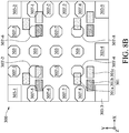
- FIG. 8B is a top-view diagram of the light-emitting unit 300 in accordance with some other embodiments of the present disclosure, and the diagram only illustrates the pixel 301 and the connection pads 303.
- some of the connection pads 303 that are electrically connected to the anode electrode of the light-emitting unit 300 may be further divided into a plurality of connection pads, e.g., the connection pad 303'- 1, 303'-2, 303'-3, 303'-4, 303'-5, 303'-6, 303'-7, and 303'-8.
- the two connection pads 303'-1 may be electrically connected to each other
- the two connection pads 303'-2 may be electrically connected to each other
- the two connection pads 303'-3 may be electrically connected to each other
- the two connection pads 303'-4 may be electrically connected to each other
- the two connection pads 303'-5 may be electrically connected to each other
- the two connection pads 303'-6 may be electrically connected to each other
- the two connection pads 303'-7 may be electrically connected to each other
- the two connection pads 303'-8 may be electrically connected to each other.
- connection pads 303'-1, 303'-2, 303'-3, 303'-4, 303' -5, 303'-6, 303'-7, and 303'-8 may be electrically connected to different anode electrodes in the light-emitting unit 300.
- the connection pads 303-1, 303-2, 303-3, 303-4, and 303-5 are electrically connected to each other, and at least one of them is electrically connected to the driving element 400.
- the connection pads 303-1, 303-2, 303-3, 303-4, and 303-5 that are not used or are not electrically connected may be regarded as redundant connection pads.
- at least one of the connection pads at the periphery of FIG. 8B may protrude from the edge 100as of the first main substrate 100a.
- connection pad that is electrically connected to the anode electrode may be suitably selected from the connection pads 303'-1, 303'-2, 303'-3, and 303'-4. Therefore, the flexibility for adjusting the wiring of the substrate may be improved or the cost for producing a variety of molds may be reduced.
- the connection pads 303'-1, 303'-2, 303'-3, and 303'-4 that are not used or are not electrically connected may be regarded as redundant connection pads.
- the bendable area of the flexible substrates may be increased or the bending angle of the flexible substrate may be reduced by having the connection pads away from the bending area where the substrates are connected, or by changing the packaging structure of the light-emitting unit or the configuration of the connection pads.
- the risk of disconnection of the circuit in the bending area of the substrate may be reduced without affecting the pitch of the light-emitting units or the resolution of the panel, thereby improving the reliability of the tiled display device.
Landscapes
- Engineering & Computer Science (AREA)
- Physics & Mathematics (AREA)
- General Physics & Mathematics (AREA)
- Theoretical Computer Science (AREA)
- Computer Hardware Design (AREA)
- Multimedia (AREA)
- Electroluminescent Light Sources (AREA)
Abstract
Description
- This application claims priority of
U.S. Provisional Patent Application No. 62/799,047 filed on January 31, 2019 201910963323.3, filed on October 11, 2019 - The present disclosure relates to a tiled display device, and in particular it relates to a tiled display device having a better connection space.
- Electronic products equipped with display panels have become indispensable necessities in modern society. With the flourishing development of these portable electronic products, consumers have high expectations regarding their quality, functionality, and price.
- Mini light-emitting diode technology is a flat panel display technology that has emerged in recent years. Mini light-emitting diode display devices can produce seamless images with wide viewing angles, high brightness, and high contrast. However, when mini light-emitting diode technology is applied to a large-sized display panel, most of them need to be tiled together to achieve a display function. As the requirements for resolution increase, the pitch between the mini light-emitting diodes decreases, which also limits the available space at the connection position of the panel.
- Although currently existing tiled display devices have been adequate for their intended purposes, they have not been satisfactory in all respects. Therefore, the development of the structural design that can improve the quality or reliability of tiled display devices is still one of the goals that the industry is currently aiming at.
- In accordance with some embodiments of the present disclosure, a tiled display device is provided. The tiled display device includes a first substrate, a second substrate and a light-emitting unit. The first substrate includes a first main substrate and a first flexible substrate. The first flexible substrate is disposed on the first main substrate. The second substrate is disposed adjacent to the first substrate. The light-emitting unit is disposed on the first flexible substrate. In addition, a portion of the light-emitting unit protrudes from an edge of the first main substrate.
- A detailed description is given in the following embodiments with reference to the accompanying drawings.
- The disclosure may be more fully understood by reading the subsequent detailed description and examples with references made to the accompanying drawings, wherein:
-
FIG. 1A is a top-view diagram of the tiled display device in accordance with some embodiments of the present disclosure; -
FIG. 1B is an enlarged cross-sectional diagram of the region A inFIG. 1A in accordance with some embodiments of the present disclosure; -
FIG. 1C is a top-view diagram of the light-emitting unit in accordance with some embodiments of the present disclosure; -
FIG. 2A is a top-view diagram of the tiled display device in accordance with some embodiments of the present disclosure; -
FIG. 2B is an enlarged cross-sectional diagram of the region A inFIG. 2A in accordance with some embodiments of the present disclosure; -
FIG. 2C is a top-view diagram of the light-emitting unit in accordance with some embodiments of the present disclosure; -
FIG. 3 is a partial cross-sectional diagram of the tiled display device in accordance with some embodiments of the present disclosure; -
FIG. 4A is a partial cross-sectional diagram of the tiled display device in accordance with some embodiments of the present disclosure; -
FIG. 4B is a top-view diagram of the light-emitting unit in accordance with some embodiments of the present disclosure; -
FIG. 5 is a top-view diagram of the tiled display device in accordance with some embodiments of the present disclosure; -
FIG. 6A is a top-view diagram of the tiled display device in accordance with some embodiments of the present disclosure; -
FIG. 6B is an enlarged cross-sectional diagram of the region A inFIG. 6A in accordance with some embodiments of the present disclosure; -
FIG. 6C is a top-view diagram of the light-emitting unit in accordance with some embodiments of the present disclosure; -
FIG. 7 is a top-view diagram of the tiled display device in accordance with some embodiments of the present disclosure; -
FIG. 8A is a top-view diagram of the light-emitting unit in accordance with some embodiments of the present disclosure; -
FIG. 8B is a top-view diagram of the light-emitting unit in accordance with some embodiments of the present disclosure. - The structure of the tiled display device of the present disclosure and the manufacturing method thereof are described in detail in the following description. In the following detailed description, for purposes of explanation, numerous specific details and embodiments are set forth in order to provide a thorough understanding of the present disclosure. The specific elements and configurations described in the following detailed description are set forth in order to clearly describe the present disclosure. It will be apparent that the exemplary embodiments set forth herein are used merely for the purpose of illustration. In addition, the drawings of different embodiments may use like and/or corresponding numerals to denote like and/or corresponding elements in order to clearly describe the present disclosure. However, the use of like and/or corresponding numerals in the drawings of different embodiments does not suggest any correlation between different embodiments.
- It should be understood that the elements or devices in the drawings of the present disclosure may be present in any form or configuration known to those with ordinary skill in the art. In addition, in the embodiments, relative expressions are used. For example, "lower", "bottom", "higher" or "top" are used to describe the position of one element relative to another. It should be appreciated that if a device is flipped upside down, an element that is "lower" will become an element that is "higher". It should be understood that the descriptions of the exemplary embodiments are intended to be read in connection with the accompanying drawings, which are to be considered part of the entire written description. The drawings are not drawn to scale. In addition, structures and devices are shown schematically in order to simplify the drawing.
- In addition, the expressions "a first material layer is disposed on or over a second material layer" may indicate that the first material layer is in direct contact with the second material layer, or that the first material layer is not in direct contact with the second material layer, there being one or more intermediate layers disposed between the first material layer and the second material layer.
- It should be understood that, although the terms first, second, third etc. may be used herein to describe various elements, components, or portions, these elements, components, or portions should not be limited by these terms. These terms are only used to distinguish one element, component, or portion from another element, component, or portion. Thus, a first element, component, or portion discussed below could be termed a second element, component, or portion without departing from the teachings of the present disclosure.
- In some embodiments of the present disclosure, terms concerning attachments, coupling and the like, such as "connected" and "interconnected", refer to a relationship wherein structures are secured or attached to one another either directly or indirectly through intervening structures, as well as both movable or rigid attachments or relationships, unless expressly described otherwise.
- Unless defined otherwise, all technical and scientific terms used herein have the same meaning as commonly understood by one of ordinary skill in the art to which this disclosure belongs. It should be appreciated that, in each case, the term, which is defined in a commonly used dictionary, should be interpreted as having a meaning that conforms to the relative skills of the present disclosure and the background or the context of the present disclosure, and should not be interpreted in an idealized or overly formal manner unless so defined.
- In accordance with some embodiments of the present disclosure, in the provided tiled display device, the bendable area of the flexible substrate may be increased by the design of the connection pad or the packaging structure of the light-emitting unit. Accordingly, the risk of disconnection of wirings at the bending portion of the flexible substrate may be reduced, or the impact on the panel resolution at the connection positions of the panels may be reduced.
- Refer to
FIG. 1A , which is a top-view diagram of atiled display device 10A in accordance with some embodiments of the present disclosure. It should be understood thatFIG. 1A only illustrates some components of thetiled display device 10A for clarity. In addition, additional features may be added to thetiled display device 10A described below in accordance with some embodiments. In accordance with some other embodiments, some of the features of thetiled display device 10A may be replaced or omitted. - In accordance with some embodiments of the present disclosure, the
tiled display device 10A may include a liquid-crystal display (LCD), a light-emitting diode (LED), a quantum dot, fluorescence, and phosphor, other suitable display media, or a combination thereof, but it is not limited thereto. In accordance with some embodiments, the light-emitting diode display device may include, for example, an organic light-emitting diode (OLED), a quantum dot light-emitting diode (QLED), and a mini light-emitting diode (mini LED), or a micro light-emitting diode (micro LED), but it is not limited thereto. - As shown in
FIG. 1A , in accordance with some embodiments, thetiled display device 10A may include afirst substrate 100 and asecond substrate 200, and thesecond substrate 200 may be disposed adjacent to thefirst substrate 100. In some embodiments, thefirst substrate 100 may include amain region 100m, anedge region 100e, and an extension region 100ex. Theedge region 100e connects between themain region 100m and the extension region 100ex. In some embodiments, thesecond substrate 200 may include amain region 200m, anedge region 200e, and an extension region 200ex. Theedge region 200e connects between themain region 200m and the extension region 200ex. In some embodiments, theedge region 100e and theedge region 200e are adjacent to each other. In some embodiments, theedge region 100e and theedge region 200e may be used as a bendable region or a region where thefirst substrate 100 and thesecond substrate 200 are connected. In some embodiments, the extension region 100ex and the extension region 200ex may be bent below thefirst substrate 100 and thesecond substrate 200. The definitions of the extension region 100ex, the extension region 200ex, theedge region 100e, theedge region 200e, themain region 100m, and themain region 200m will be further explained inFIG. 1B . - In addition, the
tiled display device 10A may include a plurality of light-emittingunits 300, and the light-emittingunits 300 may be disposed on thefirst substrate 100 and thesecond substrate 200. In some embodiments, in the normal direction of thefirst substrate 100 or the second substrate 200 (e.g., the Z direction shown in the figure), a portion of the light-emittingunit 300 may overlap with themain region 100m or themain region 200m and may not overlap with theedge region 100e or theedge region 200e; and a portion of the light-emittingunit 300 may partially overlap with themain region 100m or themain region 200m and may partially overlap with theedge region 100e of thefirst substrate 100 or theedge region 200e of thesecond substrate 200. - In some embodiments, one light-emitting
unit 300 may include or correspond to onepixel 301, but the present disclosure is not limited thereto. In accordance with some embodiments, one light-emittingunit 300 may include or correspond to a plurality ofpixels 301. In addition, thepixel 301 may include one or more subpixels. As shown inFIG. 1A , in some embodiments, one light-emittingunit 300 may include onepixel 301, and thepixel 301 may include, for example, three sub-pixels, i.e. sub-pixel 301a, sub-pixel 301b, and sub-pixel 301c. For example, in some embodiments, the sub-pixel 301a, sub-pixel 301b, and sub-pixel 301c may be red, green, and blue sub-pixels that are arranged in a suitable manner, but the present disclosure is not limited thereto. In some other embodiments, onepixel 301 may include red, green, blue, or white sub-pixels, or sub-pixels having other suitable colors, but the present disclosure is not limited thereto. In addition, in some embodiments, the sub-pixel 301a, sub-pixel 301b, and sub-pixel 301c may be the dies of light-emitting diodes that emit light of different colors, or the dies of light-emitting diode that emit light of the same color. - Moreover, a pitch P1 may exist between two
pixels 301. In detail, the term "pitch" may refer to a distance between an edge (e.g., the left-side edge) of a subpixel (e.g., sub-pixel 301a) and the same side edge (e.g., the left-side edge) of the next or the nearest same type subpixel (e.g., another sub-pixel 301a). In some embodiments, the "pitch" described above may be defined by sub-pixels that emit light of the same color. The "light of the same color" means that a wavelength difference between the maximum peaks in the spectra of the two light sources is between -5 nm to 5nm, but the present disclosure is not limited thereto. As shown inFIG. 1A , in accordance with some embodiments of the present disclosure, the light-emittingunit 300 may include onepixel 301, and thepixel 301 may include three sub-pixels. The "pitch" described above may be, for example, a distance between the left-side edge of a sub-pixel (e.g., sub-pixel 301a) in one light-emittingunit 300 and the left-side edge of the same type sub-pixel (e.g., another sub-pixel 301a) in another adjacent light-emittingunit 300. - In addition, as shown in
FIG. 1A , in accordance with some embodiments, the light-emittingunit 300 may include a plurality ofconnection pads 303. Theconnection pads 303 may be disposed on thefirst substrate 100 and thesecond substrate 200, and theconnection pads 303 may be disposed between thepixel 301 andfirst substrate 100, or between thepixel 301 and thesecond substrate 200. Theconnection pad 303 may provide electrical connection between the light-emittingunit 300 and thefirst substrate 100 and thesecond substrate 200. Specifically, in some embodiments, a layout layer (not illustrated) of various wirings or electronic circuits may be disposed on theedge region 100e of thefirst substrate 100 or theedge region 200e of thesecond substrate 200, or the front surfaces (e.g., the extension region 100ex or the extension region 200ex) or the rear surfaces (e.g., themain region 100m or themain region 200m) of thefirst substrate 100 and thesecond substrate 200. In addition, the layout layer (not illustrated) may be electrically connected to the light-emittingunit 300 through theconnection pads 303. - It should be understood that, in order to clearly illustrate the positional relationship of the light-emitting
units 300 and the connection region between thefirst substrate 100 and thesecond substrate 200, thefirst substrate 100 and thesecond substrate 200 are drawn separately. That is, the state before thefirst substrate 100 and thesecond substrate 200 are tiled (joined) is illustrated. In addition, it should be understood that although only thefirst substrate 100 and thesecond substrate 200 are illustrated in the drawings, thetiled display device 10A may include any suitable amount of the substrates as needed in accordance with some embodiments, but the present disclosure is not limited thereto. - Next, refer to
FIG. 1B , which is an enlarged cross-sectional diagram of theedge region 100e, theedge region 200e, the extension region 100ex and extension region 200ex in the region A inFIG. 1A after thefirst substrate 100 and thesecond substrate 200 are tiled (joined) in accordance with some embodiments of the present disclosure. The structure of thetiled display device 10A at the connection position is further explained as follows. As shown inFIG. 1B , thefirst substrate 100 may include a firstmain substrate 100a and a firstflexible substrate 100b, and the firstflexible substrate 100b may be disposed on the firstmain substrate 100a. Thesecond substrate 200 may include a secondmain substrate 200a and a secondflexible substrate 200b, and the secondflexible substrate 200b may be disposed on the secondmain substrate 200a. The firstmain substrate 100a may have an upper surface 100at, a lower surface 100ab, and an edge 100as. In some embodiments, the firstflexible substrate 100b may extend from the upper surface 100at to the lower surface 100ab. In some embodiments, the firstflexible substrate 100b may be optionally not in contact with the edge 100as. - Furthermore, the second
main substrate 200a may have an upper surface 200at, a lower surface 200ab, and an edge 200as. In some embodiments, the secondflexible substrate 200b may extend from the upper surface 200at to the lower surface 200ab. In some embodiments, the secondflexible substrate 200b may not be in contact with the edge 200as. - In some embodiments, the first
main substrate 100a and the secondmain substrate 200a may be a flexible substrate, a rigid substrate, or a combination thereof. In one embodiment, the material of the firstmain substrate 100a and the secondmain substrate 200a may include, but is not limited to, glass, quartz, sapphire, ceramic, plastic, other suitable substrate materials, or a combination thereof. In one embodiment, the material of the plastic substrate may include, but is not limited to, polyimide (PI), polyethylene terephthalate (PET), polycarbonate (PC), other suitable materials, or a combination thereof. In one embodiment, the material of the glass substrate may include, but is not limited to, silicon (Si), silicon carbide (SiC), gallium nitride (GaN), silicon dioxide (SiO2), other suitable materials, or a combination thereof. In addition, in some embodiments, the firstmain substrate 100a and the secondmain substrate 200a may include a metal-glass fiber composite plate or a metal-ceramic composite plate, but they are not limited thereto. Moreover, the material of the firstmain substrate 100a may be the same as or different from the material of the secondmain substrate 200a. - In some embodiments, the first
flexible substrate 100b and the secondflexible substrate 200b may include a material having flexible characteristics. For example, in some embodiments, the material of the firstflexible substrate 100b and the secondflexible substrate 200b may include, but is not limited to, polyimide (PI), polyethylene terephthalate (PET), polycarbonate (PC), other suitable materials, or a combination thereof. In addition, the material of the firstflexible substrate 100b may be the same as or different from the material of the secondflexible substrate 200b. - As described above, in some embodiments, the
first substrate 100 may include themain region 100m, the extension region 100ex, and theedge region 100e. Furthermore, themain region 100m is the region of the firstflexible substrate 100b that is adjacent to the upper surface 100at of the firstmain substrate 100a and overlaps the upper surface 100at of the firstmain substrate 100a in the normal direction of the firstmain substrate 100a (e.g., the Z direction shown in the figure). The extension region 100ex is the region of firstflexible substrate 100b that is adjacent to the lower surface 100ab of the firstmain substrate 100a and overlaps the lower surface 100ab of the firstmain substrate 100a in the normal direction of the firstmain substrate 100a. In addition, theedge region 100e is the region of the firstflexible substrate 100b excluding themain region 100m and the extension region 100ex. - As described above, in some embodiments, the
second substrate 200 may include themain region 200m, the extension region 200ex, and theedge region 200e. Furthermore, themain region 200m is the region of the secondflexible substrate 200b that is adjacent to the upper surface 200at of the secondmain substrate 200a and overlaps the upper surface 200at of the secondmain substrate 200a in the normal direction of the secondmain substrate 200a (e.g., the Z direction shown in the figure). The extension region 200ex is the region of the secondflexible substrate 200b that is adjacent to the lower surface 200ab of the secondmain substrate 200a and overlaps the lower surface 200ab of the secondmain substrate 200a in the normal direction of the secondmain substrate 200a. In addition, theedge region 200e is the region of the secondflexible substrate 200b excluding themain region 200m and the extension region 200ex. - As shown in
FIG. 1B , the light-emittingunits 300 may be disposed on the firstflexible substrate 100b, and a portion of the light-emittingunit 300 may overlap the upper surface 100at, and another portion of the light-emittingunit 300 may protrude from the upper surface 100at or the edge 100as of the firstmain substrate 100a. In other words, in some embodiments, a portion of the light-emittingunits 300 may overlap theedge region 100e in the normal direction of the firstmain substrate 100a. On the other hand, in accordance with some embodiments, the light-emittingunit 300 may also be disposed on the secondflexible substrate 200b, and a portion of the light-emittingunit 300 may overlap the upper surface 200at, and another portion of the light-emittingunit 300 may protrude from the upper surface 200at or the edge 200as of the secondmain substrate 200a. In other words, in some embodiments, a portion of the light-emittingunit 300 may overlap theedge region 200e in the normal direction of the secondmain substrate 200a. - Furthermore, in some embodiments, at least a portion of the first
flexible substrate 100b may be disposed between thefirst substrate 100 and thesecond substrate 200. Specifically, in some embodiments, at least a portion of the firstflexible substrate 100b may be disposed between the edge 100as of the firstmain substrate 100a and the edge 200as of the secondmain substrate 200a. In some embodiments, in the normal direction of the firstmain substrate 100a or the secondmain substrate 200a (e.g., the Z direction shown in the figure), a portion of the light-emittingunit 300 may overlap the firstflexible substrate 100b that is disposed between the edge 100as and the edge 200as. - Similarly, in some embodiments, at least a portion of the second
flexible substrate 200b may be disposed between thefirst substrate 100 and thesecond substrate 200, for example, between the edge 100as of the firstmain substrate 100a and the edge 200as of the secondmain substrate 200a. - As described above, in accordance with some embodiments, the light-emitting
unit 300 may include one ormore pixels 301, and thepixel 301 may include a suitable number of sub-pixels, such as sub-pixel 301a, sub-pixel 301b, and sub-pixel 310c. In this embodiment, the light-emittingunit 300 may include onepixel 301, and thepixel 301 may include three sub-pixels. In some embodiments, the sub-pixel 301a, the sub-pixel 301b, and the sub-pixel 310c are three dies of the light-emitting diodes. - In addition, as shown in
FIG. 1B , in some embodiments, the light-emittingunit 300 may include a plurality ofconnection pads 303, and theconnection pads 303 may be disposed on the firstflexible substrate 100b and the secondflexible substrate 200b. In some embodiments, the firstflexible substrate 100b and the secondflexible substrate 200b may include a layout layer (not illustrated) of various wirings or electronic circuits disposed thereon, and the layout layer (not illustrated) may be electrically connected to the light-emittingunits 300 through theconnection pads 303. - In some embodiments, the
connection pad 303 may be electrically connected to an anode electrode or a cathode electrode of the die of the light-emittingunit 300. Specifically, in this embodiment, the light-emittingunit 300 has three sub-pixels, i.e. sub-pixel 301a, sub-pixel 301b, and sub-pixel 310c. The threeconnection pads 303 may be electrically connected to the anode electrodes of the dies of the sub-pixel 301a, sub-pixel 301b, and sub-pixel 310c, and oneconnection pad 303 may be electrically connected to the cathode electrode of the dies of the sub-pixel 301a, sub-pixel 301b, and sub-pixel 310c. That is, the three sub-pixels 301a, 301b, and 310c may have a common cathode, but the manner of polarity connection is not limited thereto. - In some embodiments, the
connection pad 303 may include a conductive material. In some embodiments, theconnection pad 303 may include a metal conductive material, a transparent conductive material, or a combination thereof. In some embodiments, the metal conductive material may include, but is not limited to, copper (Cu), aluminum (Al), molybdenum (Mo), silver (Ag), tin (Sn), tungsten (W), gold (Au), chromium (Cr), nickel (Ni), platinum (Pt), copper alloy, aluminum alloy, molybdenum alloy, silver alloy, tin alloy, tungsten alloy, gold alloy, chromium alloy, nickel alloy, platinum alloy, other suitable metal materials, or a combination thereof. In some embodiments, the transparent conductive material may include a transparent conductive oxide (TCO). For example, the transparent conductive oxide may include, but is not limited to, indium tin oxide (ITO), tin oxide (SnO), zinc oxide (ZnO), indium zinc oxide (IZO), indium gallium zinc oxide (IGZO), indium tin zinc oxide (ITZO), antimony tin oxide (ATO), antimony zinc oxide (AZO), other suitable transparent conductive materials, or a combination thereof. - In some embodiments, a chemical vapor deposition (CVD) process, a physical vapor deposition (PVD) process, an electroplating process, an electroless plating process, other suitable processes, or a combination thereof may be used to form the
connection pad 303, but the present disclosure is not limited thereto. - In addition, in accordance with some embodiments, the light-emitting
unit 300 may further include anintermediate substrate 305 disposed between thepixel 301 and theconnection pad 303, and aprotective layer 307 disposed above theintermediate substrate 305. In some embodiments, thepixel 301 may be electrically connected to theconnection pad 303 through a via (not illustrated) that penetrates through theintermediate substrate 305, but it is not limited thereto. In some embodiments, theprotective layer 307 may optionally cover the top surface and the side surface of thepixel 301. - In some embodiments, the
intermediate substrate 305 may be a flexible substrate, a rigid substrate, or a combination thereof. In one embodiment, theintermediate substrate 305 may include, but is not limited to, a glass substrate, a ceramic substrate, a plastic substrate, other suitable substrate materials, or a combination thereof. In one embodiment, the material of theintermediate substrate 305 may include, but is not limited to, epoxy resins, polymerized siloxanes (silicone), polyimide (PI), and polyethylene terephthalate (PET), polycarbonate (PC), other suitable materials, or a combination thereof. In one embodiment, the material of the glass substrate may include, but is not limited to, silicon (Si), silicon carbide (SiC), gallium nitride (GaN), silicon dioxide (SiO2), other suitable materials, or a combination thereof. In addition, in some embodiments, theintermediate substrate 305 may include a printed circuit board (PCB), a metal-glass fiber composite plate, or a metal-ceramic composite plate, but it is not limited thereto. - In some embodiments, the
protective layer 307 may include, but is not limited to, organic materials, inorganic materials, other suitable packaging materials, or a combination thereof. In some embodiments, the inorganic material may include, but is not limited to, silicon nitride, silicon oxide, silicon oxynitride, aluminum oxide, or other suitable materials. In some embodiments, the organic material may include, but is not limited to, epoxy resins, silicone resins, acrylic resins (such as polymethylmetacrylate (PMMA), benzocyclobutene (BCB), polyimide, polyester, polydimethylsiloxane (PDMS), tetrafluoroethylene-perfluoroalkoxy vinyl ether copolymer (polyfluoroalkoxy, PFA), other suitable materials, or a combination thereof. - In addition, in accordance with some embodiments, the
protective layer 307 may have a function of wavelength conversion, for example, a light source generated by thepixel 301 may be converted into light having a specific wavelength range (specific color). In some embodiments, theprotective layer 307 may further include particles having a wavelength conversion function, such as phosphors, quantum dot (QD) materials, organic fluorescent materials, other suitable materials, or a combination thereof, but it is not limited thereto. - In some embodiments, the
protective layer 307 may be formed by the chemical vapor deposition process, a spin coating process, a printing process, other suitable processes, or a combination thereof. - In accordance with some embodiments, the packaging method of the light-emitting
unit 300 may include surface-mount devices (SMD) packaging of light-emitting diodes, chip-on-board (COB) packaging of light-emitting diodes, packaging of micro light-emitting diodes or flip-chip light-emitting diodes, packaging of organic light-emitting diodes, other suitable packaging methods, or a combination thereof, but it is not limited thereto. - In addition, as shown in
FIG. 1B , in accordance with some embodiments, the tiled display device 10 may further include a drivingelement 400, and the drivingelement 400 may be disposed on the extension region 100ex of the firstflexible substrate 100b. In some embodiments, the drivingelement 400 may be in contact with the lower surface 100bb of the firstflexible substrate 100b. In some embodiments, the drivingelement 400 may also be disposed on the extension region 200ex of the secondflexible substrate 200b, and may be in contact with the lower surface 200bb of the secondflexible substrate 200b. - In some embodiments, the driving
element 400 may include an active driving element, a passive driving element, or a combination thereof. For example, the active driving element may include a thin-film transistor (TFT), but it is not limited thereto. For example, the thin film transistor may include a switching transistor, a driving transistor, a reset transistor, or other thin film transistors. In some embodiments, the thin film transistor may include at least one semiconductor layer. The semiconductor layer may include, but is not limited to, amorphous silicon, such as low-temperature polysilicon (LTPS), metal oxide, other suitable materials, or a combination thereof. The metal oxide may include, but is not limited to, indium gallium zinc oxide (IGZO), indium zinc oxide (IZO), indium gallium zinc tin oxide (IGZTO), other suitable materials, or a combination thereof. - Furthermore, in the embodiments where the driving element is a passive driving element, the driving element may be controlled by, for example, an integrated circuit (IC) or a microchip, but the present disclosure is not limited thereto.
- Next, refer to both
FIG. 1B and FIG. 1C. FIG. 1C is a top-view diagram of the light-emittingunit 300 in accordance with some embodiments of the present disclosure. The diagram only illustrates thepixel 301 and theconnection pads 303. As shown inFIG. 1B and FIG. 1C , in some embodiments, theconnection pad 303 may not overlap with theedge region 100e or theedge region 200e in the normal direction (e.g., the Z direction shown in the figure) of the firstmain substrate 100a. Specifically, in some embodiments, thesidewall 303s of theconnection pad 303 may not be aligned with the sidewall of the light-emitting unit 300 (e.g., thesidewall 305s of theintermediate substrate 305 or thesidewall 307s of the protective layer 307). In addition, theside wall 303s, theside wall 305s, and theside wall 307s respectively refer to the side wall of theconnection pad 303, the side wall of theintermediate substrate 305, and the side wall of theprotective layer 307 that are closer to the connection position of thefirst substrate 100 and thesecond substrate 200. - In some embodiments, the
connection pads 303 may be shifted, that is, theconnection pads 303 may be unevenly disposed at the four corners of the light-emittingunit 300, but each sub-pixels 301a, 301b, and 301c of the light-emittingunit 300 is electrically connected to thecorresponding connection pad 303 through the wirings in theintermediate substrate 305. For example, the sub-pixel 301c may be electrically connected to the two connection pads (i.e.connection pad 303c andconnection pad 303z) through the wirings in theintermediate substrate 305. Theconnection pad 303z may be a common cathode, therefore the sub-pixel 301a and sub-pixel 301b may also be electrically connected to theconnection pad 303z. In some embodiments, theconnection pads 303 of the light-emittingunits 300 other than those partially overlapping theedge region 100e may be uniformly disposed at four corners of the light-emittingunit 300 or uniformly disposed at the periphery of the light-emittingunit 300, but the present disclosure is not limited thereto. In some embodiments, some sub-pixels (e.g., the sub-pixel 301c shown in the figure) may protrude from the edge 100as of the firstmain substrate 100a and partially overlap theedge region 100e in the normal direction of the firstmain substrate 100a (e.g., the Z direction shown in the figure). Moreover, in some embodiments, some sub-pixels (e.g., the sub-pixel 301a shown in the figure) may protrude from the edge 200as of the secondmain substrate 200a and partially overlap theedge region 200e in the normal direction of the secondmain substrate 200a (e.g., the Z direction shown in the figure). - In addition, in some embodiments, the
connection pad 303 may not protrude from the edge 100as of the firstmain substrate 100a in the normal direction of the firstmain substrate 100a (e.g., the Z direction shown in the figure). In some embodiments, theconnection pad 303 may not protrude from the edge 200as of the secondmain substrate 200a in the normal direction of the secondmain substrate 200a (e.g., the Z direction shown in the figure). - It should be noted that in accordance with some embodiments of the present disclosure, a portion of the light-emitting
unit 300 that is near the connection position may protrude from the edge 100as of the firstmain substrate 100a or the edge 200as of the secondmain substrate 200a. In general tiled display devices, the sidewall of the light-emittingunit 300 is aligned with the edge 100as or the edge 200as, or the light-emittingunit 300 does not protrude from the edge 100as or the edge 200as. Compared with general tiled display devices, the configuration of the light-emittingunits 300 and theconnection pads 303 provided in the present disclosure renders at least a portion of theedge region 100e of the firstflexible substrate 100b and at least a portion of theedge region 200e of the secondflexible substrate 200b hidden under the light-emittingunits 300. Therefore, the bendable space SP of the firstflexible substrate 100b and the secondflexible substrate 200b at the connection position may be increased, and the risk of disconnection of the wirings at the bending positions of the firstflexible substrate 100b or the secondflexible substrate 200b may be reduced. Specifically, the bendable space SP of the firstflexible substrate 100b and the secondflexible substrate 200b at the connection position of the substrates may be the minimum distance between the edge 100as of the firstmain substrate 100a and the edges 200as of the secondmain substrate 200a. Alternatively, in accordance with some embodiments of the present disclosure, the configuration of the light-emittingunit 300 and itsconnection pads 303 may reduce the difference between the pitch P1 of thepixels 301 in themain region 100m and the pitch P11 of thepixels 301 that are adjacent to the connection position of the substrates, thereby reducing the visual gap at the connection position or improving the display quality. - Next, refer to
FIG. 2A , which is a top-view diagram of atiled display device 10B in accordance with some other embodiments of the present disclosure. It should be understood that the same or similar components or elements in above and below contexts are represented by the same or similar reference numerals. The materials, manufacturing methods and functions of these components or elements are the same or similar to those described above, and thus will not be repeated herein. - As shown in
FIG. 2A , in accordance with some embodiments, thefirst substrate 100 may include at least oneedge region 100e. In other words, thefirst substrate 100 may include a plurality of regions that can serve as the bendable connection position. In some embodiments, thesecond substrate 200 may include at least oneedge region 200e. In other words, thesecond substrate 200 may include a plurality of regions that may serve as the bendable connection position. Specifically, in this embodiment, thefirst substrate 100 and thesecond substrate 200 may have, for example, fouredge regions 100e and fouredge regions 200e, respectively. The four sides of thefirst substrate 100 and thesecond substrate 200 may be tiled with other substrates. In addition, in this embodiment, the light-emittingunits 300 provided on thefirst substrate 100 and the light-emittingunits 300 provided on thesecond substrate 200 may have the same configuration ofconnection pads 303. - Specifically, refer to
FIG. 2B and FIG. 2C. FIG. 2B is an enlarged cross-sectional diagram of theedge region 100e, theedge region 200e, the extension region 100ex and extension region 200ex in the region A inFIG. 2A .FIG. 2C is a top-view diagram of the light-emittingunit 300 in accordance with some embodiments of the present disclosure. The diagram only illustrates thepixel 301 and theconnection pads 303. As shown inFIG. 2B and FIG. 2C , in this embodiment, theconnection pads 303 may be disposed near the center of the light-emittingunit 300, and theconnection pads 303 may not be disposed at the four corners of the light-emittingunit 300. In this embodiment, thesidewall 303s of theconnection pad 303 may not be aligned with the sidewall of the light-emitting unit 300 (e.g., thesidewall 305s of theintermediate substrate 305 or thesidewall 307s of the protective layer 307). In addition, theconnection pad 303 may not overlap with theedge region 100e or theedge region 200e in the normal direction of the firstmain substrate 100a (e.g., the Z direction shown in the figure), and a portion of the light-emittingunit 300 may protrude from the edge 100as of the firstmain substrate 100a. - In some embodiments, in the normal direction of the first
main substrate 100a (e.g., the Z direction shown in the figure), a portion of the sub-pixel that is adjacent to theedge region 100e (e.g., the sub-pixel 301c shown in the figure) may overlap themain region 100m, and another portion of which may protrude from the edge 100as of the firstmain substrate 100a and overlap with theedge region 100e. Furthermore, in some embodiments, in the normal direction of the secondmain substrate 200a (e.g., the Z direction shown in the figure), a portion of the sub-pixel that is adjacent to theedge region 100e (e.g., the sub-pixel 301a shown in the figure) may overlap themain region 200m, and another portion of which may protrude from the edge 200as of the secondmain substrate 200a and overlap theedge region 200e. - In addition, in some embodiments, the
connection pads 303 may not protrude from the edge 100as of the firstmain substrate 100a in the normal direction of the firstmain substrate 100a (e.g., the Z direction shown in the figure). That is, theconnection pads 303 may be substantially disposed on themain region 100m. In some embodiments, theconnection pads 303 may not protrude from the edge 200as of the secondmain substrate 200a in the normal direction of the secondmain substrate 200a (e.g., the Z direction shown in the figure). That is, theconnection pads 303 may be substantially disposed on themain region 200m. - It should be noted that in this embodiment, a portion of the light-emitting
unit 300 that is near the connection position may protrude from the edge 100as of the firstmain substrate 100a or the edge 200as of the secondmain substrate 200a. The configuration of the light-emittingunits 300 and theconnection pads 303 described above may increase the bendable space SP of the firstflexible substrate 100b and the secondflexible substrate 200b at the connection position of the substrates, thereby reducing risk of disconnection of the wirings at the bending position of the firstflexible substrate 100b or the secondflexible substrate 200b. Alternatively, the configuration of the light-emittingunit 300 and itsconnection pads 303 may reduce the difference between the pitch P1 of thepixels 301 in themain region 100m and the pitch P11 of thepixels 301 that are adjacent to the connection position of the substrates, thereby reducing the visual gap at the connection position or improving the display quality. - In addition, in this embodiment, the
connection pads 303 are all disposed near the center of the light-emittingunit 300. Therefore, in cases where thefirst substrate 100 and thesecond substrate 200 haveseveral edge regions 100e andedge regions 200e, only one type of light-emittingunit 300 may be provided, which may reduce the cost and difficulty of manufacturing. - Next, refer to
FIG. 3 , which is a partial cross-sectional diagram of atiled display device 10C in accordance with some embodiments of the present disclosure. Specifically,FIG. 3 illustrates a partial structure of thetiled display device 10C at the connection position of thefirst substrate 100 and thesecond substrate 200. As shown inFIG. 3 , in this embodiment, a maximum distance between thepixel 301 and theconnection pad 303 in the X direction may be increased by increasing the packaging volume of the light-emittingunit 300. For example, compared with thepixel 301, theconnection pads 303 may be farther away from the connection position of thefirst substrate 100 and thesecond substrate 200. In this embodiment, the volume of the light-emittingunit 300 may be increased by increasing the volume of theintermediate substrate 305 and theprotective layer 307, so that a portion of the light-emittingunit 300 may protrude from the edge 100as of the firstmain substrate 100a. - Similarly, in this embodiment, the
sidewall 303s of theconnection pad 303 may not be aligned with the sidewall of the light-emitting unit 300 (e.g., thesidewall 305s of theintermediate substrate 305 or thesidewall 307s of the protective layer 307). Theconnection pads 303 may be disposed away from the side of thefirst substrate 100 or the side of thesecond substrate 200, or theconnection pads 303 may be disposed at a position away from the connection position of thefirst substrate 100 and thesecond substrate 200. - In some embodiments, in the normal direction of the first
main substrate 100a (e.g., the Z direction shown in the figure), some sub-pixels (e.g., the sub-pixel 301c and the sub-pixel 301b shown in the figure) may protrude from the edge 100as of the firstmain substrate 100a and overlap theedge region 100e. Furthermore, in some embodiments, in the normal direction of the secondmain substrate 200a (e.g., the Z direction shown in the figure), some sub-pixels (e.g., the sub-pixel 301a and the sub-pixel 301b shown in the figure) may protrude from the edge 200as of the secondmain substrate 200a and overlap theedge region 200e. - In addition, in some embodiments, the
connection pads 303 may not protrude from the edge 100as of the firstmain substrate 100a in the normal direction of the firstmain substrate 100a (e.g., the Z direction shown in the figure). That is, theconnection pads 303 may be substantially disposed on themain region 100m. In some embodiments, theconnection pads 303 may not protrude from the edge 200as of the secondmain substrate 200a in the normal direction of the secondmain substrate 200a (e.g., the Z direction shown in the figure). That is, theconnection pads 303 may be substantially disposed on themain region 200m. - In addition, as shown in
FIG. 3 , in some embodiments, the light-emittingunit 300 may further include aredundant connection pad 303r, and at least a portion of theredundant connection pad 303r may protrude from the edge 100as of the firstmain substrate 100a. In some embodiments, theredundant connection pad 303r is a connection pad that is not electrically connected to thepixel 301 or the circuit (not illustrated) on the firstflexible substrate 100b. In some embodiments, theredundant connection pad 303r of the light-emittingunit 300 may be in contact with the redundant connection pad (not illustrated) disposed on theedge region 100e of the firstflexible substrate 100b to increase the structural strength or stability of the light-emittingunit 300. For example, when the light-emittingunit 300 is fixed on thesubstrate 100, the redundant connection pad may provide a uniform pressure distribution. In some embodiments, the material of theredundant connection pad 303r may be the same or similar to the material of theconnection pad 303 as described above, and thus will not be repeated herein. - In this embodiment, a portion of the light-emitting
unit 300 that is near the connection position may protrude from the edge 100as of the firstmain substrate 100a or the edge 200as of the secondmain substrate 200a, which renders theedge region 100e of the firstflexible substrate 100b and theedge region 200e of the secondflexible substrate 200b hidden under the light-emittingunits 300. Therefore, the bendable space SP of the firstflexible substrate 100b and the secondflexible substrate 200b at the connection position may be increased, and the risk of disconnection of the wirings at the bending positions of the firstflexible substrate 100b or the secondflexible substrate 200b may be reduced. Alternatively, in this embodiments, the configuration of the light-emittingunit 300 and itsconnection pads 303 may reduce the difference between the pitch P1 of thepixels 301 in themain region 100m and the pitch P11 of thepixels 301 that are adjacent to the connection position of the substrates, thereby reducing the visual gap at the connection position or improving the display quality. - Next, refer to
FIG. 4A and FIG. 4B. FIG. 4A is a partial cross-sectional diagram of atiled display device 10D in accordance with some embodiments of the present disclosure. Specifically,FIG. 4A illustrates a partial structure of thetiled display device 10D at the connection position of thefirst substrate 100 and thesecond substrate 200.FIG. 4B is a top-view diagram of some light-emittingunits 300 in this embodiment, and the diagram only illustrates thepixel 301 and theconnection pads 303. - As shown in
FIG. 4A , in some embodiments, the configurations of theconnection pads 303 of different light-emitting units 300 (labeled as light-emitting unit 300-1 and light-emitting unit 300-2 for clear illustration) may be different. In some embodiments, the configuration of theconnection pads 303 of the light-emitting unit 300-1 located on themain region 100m may be different from the configuration of theconnection pads 303 of the light-emitting unit 300-2 located on theedge area 100e. - Specifically, in this embodiment, the configuration of the
connection pads 303 corresponding to the light-emitting unit 300-1 is as shown inFIG. 4B . Theconnection pads 303 may be substantially disposed at four corners of the light-emittingunit 300. In some embodiments, some of the sub-pixels (e.g., the sub-pixel 301b) of the light-emitting unit 300-1 do not overlap theconnection pads 303 in the normal direction (e.g., the Z direction shown in the figure) of the firstmain substrate 100a. Furthermore, in this embodiment, the configuration of theconnection pads 303 corresponding to the light-emitting unit 300-2 may be as shown in the aboveFIG. 1C , but the present disclosure is not limited thereto. - It should be understood that in accordance with some embodiments, in the
tiled display device 10D, the configurations of theconnection pads 303 of some of the light-emittingunits 300 may be the same, and the configurations of theconnection pads 303 of some light-emittingunits 300 may different. In addition, in accordance with some embodiments, in thetiled display device 10D, the packaging structures (e.g., the volume of the package) of some of the light-emittingunits 300 may be the same, and the packaging structures of some of the light-emittingunits 300 may be different. - Next, refer to
FIG. 5 , which is a top-view diagram of atiled display device 10E in accordance with some other embodiments of the present disclosure. As shown inFIG. 5 , in some embodiments, the light-emittingunit 300 may havedifferent connection pads 303 configurations according to different positions on thefirst substrate 100. - For example, in this embodiment, the
connection pads 303 of the light-emittingunit 300 located on theedge region 100e are substantially as shown inFIG. 1C . That is, theconnection pads 303 may be gathered toward a particular direction. Furthermore, in this embodiment, the light-emittingunits 300 located between the twoedge regions 100e may be gathered toward one corner, but the present disclosure is not limited thereto. - Next, refer to
FIG. 6A , which is a top-view diagram of atiled display device 10F in accordance with some embodiments of the present disclosure. As shown inFIG. 6A , in some embodiments, the sides of thefirst substrate 100 or thesecond substrate 200 may partially include theedge region 100e, the extension region 100ex, theedge region 200e, or the extension region 200ex, as the bendable areas for connection. Furthermore, in this embodiment, thetiled display device 10F may include the light-emittingunits 300 having different packaging structures. For example, the light-emitting unit 300-1 shown in the figure may include two sets of pixels 301 (labeled as pixel 301-1 and pixel 301-2), and the light-emitting unit 300-2 may include one set pixel 301 (labeled as pixel 301-1). In addition, in some embodiments, the configuration of theconnection pads 303 in the light-emitting unit 300-1 may be different from the configuration of theconnection pads 303 in the light-emitting unit 300-2. - Refer to
FIG. 6B and FIG. 6C. FIG. 6B is an enlarged cross-sectional diagram of the region A inFIG. 6A .FIG. 6C is a top-view diagram of the light-emittingunit 300 in this embodiment, and the diagram only illustrates thepixel 301 and theconnection pads 303. In this embodiment, the light-emittingunit 300 may include the pixel 301-1 and the pixel 301-2. The pixel 301-1 may be located on the firstmain substrate 100a, and a portion of the pixel 301-2 may protrude from the edge 100as of the firstmain substrate 100a. Specifically, in this embodiment, by increasing the packaging volume of the light-emittingunit 300, the light-emittingunit 300 may accommodate a plurality of pixels 301 (e.g., the pixel 301-1 and the pixel 301-2), and theconnection pads 303 may be farther away from the connection position of thefirst substrate 100 and thesecond substrate 200 compared with the pixel 301 (pixel 301-2). - In this embodiment, the volume of the light-emitting
unit 300 may be increased by increasing the volume of theintermediate substrate 305 and theprotective layer 307, so that a portion of the light-emittingunit 300 may protrude from the edge 100as of the firstmain substrate 100a. Specifically, in some embodiments, a portion of the light-emittingunit 300 may protrude from the edge 100as for a distance d. In some embodiments, the light-emittingunit 300 has a maximum length L in the X direction, and the length L may be, for example, a distance from one side of theintermediate substrate 305 to the other side in the x direction. In some embodiments, the distance d may be less than or equal to L/2, or in a range between L/5 and L/3. - It should be understood that if the distance d is too large, the light-emitting
unit 300 may not be stably mounted on the firstflexible substrate 100b; on the other hand, if the distance d is too small, the bendable space SP of the firstflexible substrate 100b and the secondflexible substrate 200b at the connection position may be insufficient. Furthermore, in accordance with some embodiments, the distance d may refer to a maximum distance between the edge 100as of the firstmain substrate 100a and the side wall of the light-emitting unit 300 (e.g., theside wall 305s of theintermediate substrate 305 or theside wall 307s of the protective layer 307) in a direction perpendicular to the normal direction of the firstmain substrate 100a (e.g., the X direction shown in the figure). - In addition, in accordance with some embodiments of the present disclosure, an optical microscopy (OM), a scanning electron microscope (SEM), a film thickness profiler (a-step), an ellipsometer, or other suitable methods may be used to measure the thickness or length of the elements, or distance between the elements, but the present disclosure is not limited thereto.
- As shown in
FIG. 6B and FIG. 6C , in this embodiment, thesidewall 303s of theconnection pad 303 may not be aligned with the sidewall of the light-emitting unit 300 (e.g., thesidewall 305s of theintermediate substrate 305 or thesidewall 307s of the protective layer 307), and theconnection pads 303 may be disposed far from the connection position of thefirst substrate 100 and thesecond substrate 200. In addition, in accordance with some embodiments, the configuration of theconnection pads 303 corresponding to the pixel 301-1 may be different from the configuration of theconnection pads 303 corresponding to the pixel 301-2. - Furthermore, in this embodiment, the light-emitting
unit 300 may further include theredundant connection pads 303r, and at least a portion of theredundant connection pad 303r may protrude from the edge 100as of the firstmain substrate 100a. In some embodiments, theredundant connection pad 303r may not be electrically connected to thepixel 301 or the circuit (not illustrated) on the firstflexible substrate 100b. In some embodiments, theredundant connection pad 303r of the light-emittingunit 300 may be in contact with the redundant connection pad (not illustrated) disposed on theedge region 100e of the firstflexible substrate 100b to increase structural strength or stability. - In this embodiment, a portion of the light-emitting
unit 300 that is near the connection position may protrude from the edge 100as of the firstmain substrate 100a or the edge 200as of the secondmain substrate 200a, thereby increasing the bendable space SP of the firstflexible substrate 100b and the secondflexible substrate 200b at the connection position. Therefore, the risk of disconnection of the wirings at the bending positions of the firstflexible substrate 100b or the secondflexible substrate 200b may be reduced. Moreover, in this embodiment, the configuration described above may maintain the consistency of the pitch P1 between thepixels 301, even at the connection position of the substrates. - Next, refer to
FIG. 7 , which is a top-view diagram of atiled display device 10G in accordance with some other embodiments of the present disclosure. As shown inFIG. 7 , in some embodiments, thetiled display device 10G may include the light-emittingunits 300 having different packaging structures. For example, the light-emitting unit 300-1 shown in the figure may include two sets of pixels 301 (labeled as pixel 301-1 and pixel 301-2), the light-emitting unit 300-2 may include one set of pixel 301 (labeled as pixel 301-1), and the light-emitting unit 300-3 may include four sets of pixels 301 (labeled as pixel 301-1, pixel 301-2, pixel 301-3, and pixel 301-4). - In addition, in some embodiments, the configurations of the
connection pads 303 in the light-emitting unit 300-1, the light-emitting unit 300-2, and light-emitting unit 300-3 may be different from each other. Specifically, in some embodiments, the configuration of theconnection pads 303 in the light-emitting unit 300-1 may be as shown inFIG. 6C , and the configuration of theconnection pads 303 in the light-emitting unit 300-2 may be as shown inFIG. 4B , but the present disclosure is not limited thereto. As described above, in this embodiment, the light-emitting unit 300-3 may include four sets ofpixels 301, and thepixel 301 may include, for example, 12 sub-pixels. As shown inFIG. 7 , the light-emitting unit 300-3 may include 13connection pads 303, one of the connection pads 303 (e.g., theconnection pad 303 located at the center) may be electrically connected to the common cathode of the sub-pixel, but the present disclosure is not limited thereto. - Next, refer to
FIG. 8A , which is a top-view diagram of the light-emittingunit 300 in accordance with some embodiments of the present disclosure, and the diagram only illustrates thepixel 301 and theconnection pads 303. As shown inFIG. 8A , in some embodiments, the light-emittingunit 300 may include four sets ofpixels 301, and eachpixel 301 may include three sub-pixels (sub-pixel 301a, sub-pixel 301b, and sub-pixel 301c). That is, the light-emittingunit 300 may include 12 sub-pixels. In this embodiment, the anode electrodes of the twelve sub-pixels may be respectively electrically connected to the twelveconnection pads 303 located in the central area, so as to respectively control the twelve sub-pixels. Furthermore, in this embodiment, the eight connection pads 303-1, 303-2, 303-3, 303-4, 303-5, 303-6, 303-7, and 303-8 provided in the peripheral area may be electrically connected to each other, and at least one of them may be electrically connected to the common cathode electrode of the twelve sub-pixels. - In addition, in some embodiments, at least one of the connection pads 303-1, 303-2, 303-3, 303-4, 303-5, 303-6, 303-7, and 303-8 may be electrically connected to the driving
element 400 disposed on the lower surface 100bb of the firstflexible substrate 100b. It should be noted that in this embodiment, according to theedge area 100e at different positions or the bendable area at different orientations, the connection pad that is electrically connected to the cathode electrode or the drivingelement 400 may be suitably selected from the connection pads 303-1, 303-2, 303-3, 303-4, 303-5, 303-6, 303-7, and 303-8. Therefore, the flexibility for adjusting the wiring of the substrate may be improved or the cost for producing a variety of molds may be reduced. In some embodiments, at least one of the above eight connection pads may protrude from the edge 100as of the firstmain substrate 100a. In some embodiments, the connection pads 303-1, 303-2, 303-3, 303-4, 303-5, 303-6, 303-7, and 303-8 that are not used or are not electrically connected may be regarded as redundant connection pads. - In addition, it should be understood that although the
connection pad 303 shown in the drawings has a rectangular or octagonal shape, the present disclosure is not limited thereto. In some embodiments, the shape of theconnection pad 303 may be adjusted according to actual needs. For example, theconnection pad 303 may have a triangle, a square, a circle, a pentagon, a hexagon, an arbitrary polygon, other suitable shapes, or a combination thereof, but it is not limited thereto. - Next, refer to
FIG. 8B , which is a top-view diagram of the light-emittingunit 300 in accordance with some other embodiments of the present disclosure, and the diagram only illustrates thepixel 301 and theconnection pads 303. As shown inFIG. 8B , in accordance with some embodiments, some of theconnection pads 303 that are electrically connected to the anode electrode of the light-emittingunit 300 may be further divided into a plurality of connection pads, e.g., the connection pad 303'- 1, 303'-2, 303'-3, 303'-4, 303'-5, 303'-6, 303'-7, and 303'-8. In some embodiments, the two connection pads 303'-1 may be electrically connected to each other, the two connection pads 303'-2 may be electrically connected to each other, the two connection pads 303'-3 may be electrically connected to each other, the two connection pads 303'-4 may be electrically connected to each other, the two connection pads 303'-5 may be electrically connected to each other, the two connection pads 303'-6 may be electrically connected to each other, the two connection pads 303'-7 may be electrically connected to each other, and the two connection pads 303'-8 may be electrically connected to each other. In some embodiments, the connection pads 303'-1, 303'-2, 303'-3, 303'-4, 303' -5, 303'-6, 303'-7, and 303'-8 may be electrically connected to different anode electrodes in the light-emittingunit 300. In some embodiments, the connection pads 303-1, 303-2, 303-3, 303-4, and 303-5 are electrically connected to each other, and at least one of them is electrically connected to the drivingelement 400. In some embodiments, the connection pads 303-1, 303-2, 303-3, 303-4, and 303-5 that are not used or are not electrically connected may be regarded as redundant connection pads. In some embodiments, at least one of the connection pads at the periphery ofFIG. 8B may protrude from the edge 100as of the firstmain substrate 100a. - It should be noted that in this embodiment, according to the
edge area 100e at different positions or the bendable area at different orientations, the connection pad that is electrically connected to the anode electrode may be suitably selected from the connection pads 303'-1, 303'-2, 303'-3, and 303'-4. Therefore, the flexibility for adjusting the wiring of the substrate may be improved or the cost for producing a variety of molds may be reduced. In some embodiments, the connection pads 303'-1, 303'-2, 303'-3, and 303'-4 that are not used or are not electrically connected may be regarded as redundant connection pads. - To summarize the above, in accordance with some embodiments of the present disclosure, the bendable area of the flexible substrates may be increased or the bending angle of the flexible substrate may be reduced by having the connection pads away from the bending area where the substrates are connected, or by changing the packaging structure of the light-emitting unit or the configuration of the connection pads. In accordance with some embodiments of the present disclosure, the risk of disconnection of the circuit in the bending area of the substrate may be reduced without affecting the pitch of the light-emitting units or the resolution of the panel, thereby improving the reliability of the tiled display device.
- Although some embodiments of the present disclosure and their advantages have been described in detail, it should be understood that various changes, substitutions and alterations can be made herein without departing from the spirit and scope of the disclosure as defined by the appended claims. Moreover, the scope of the present application is not intended to be limited to the particular embodiments of the process, machine, manufacture, composition of matter, means, methods and steps described in the specification. As one of ordinary skill in the art will readily appreciate from the present disclosure, processes, machines, manufacture, compositions of matter, means, methods, or steps, presently existing or later to be developed, that perform substantially the same function or achieve substantially the same result as the corresponding embodiments described herein may be utilized according to the present disclosure. Accordingly, the appended claims are intended to include within their scope such processes, machines, manufacture, compositions of matter, means, methods, or steps. In addition, each claim constitutes an individual embodiment, and the claimed scope of the present disclosure also includes the combinations of the claims and embodiments. The features of the various embodiments can be used in any combination as long as they do not depart from the spirit and scope of the present disclosure. The scope of protection of present disclosure is subject to the definition of the scope of the appended claims.
Claims (15)
- A tiled display device (10A, 10B, 10C, 10D, 10E, 10F, 10G), comprising:a first substrate (100) comprising a first main substrate (100a) and a first flexible substrate (100b), wherein the first flexible substrate is disposed on the first main substrate;a second substrate (200) disposed adjacent to the first substrate; anda light-emitting unit (300) disposed on the first flexible substrate,wherein a portion of the light-emitting unit protrudes from an edge (100as) of the first main substrate.
- The tiled display device as claimed in claim 1, wherein at least a portion of the first flexible substrate is disposed between the first substrate and the second substrate.
- The tiled display device as claimed in claims 1 or 2, the light-emitting unit comprising a plurality of connection pads (303), wherein at least one of the plurality of connection pads protrudes from the edge of the first main substrate.
- The tiled display device as claimed in claim 3, wherein a sidewall (303s) of at least one of the plurality of connection pads is not aligned with a sidewall of the light-emitting unit.
- The tiled display device as claimed in any of the claims 1 to 2, the light-emitting unit comprising a plurality of connection pads, wherein at least two of the plurality of connection pads are electrically connected to each other.
- The tiled display device as claimed in any of the claims 1 to 5, wherein the light-emitting unit comprises at least one pixel (301).
or wherein the light-emitting unit comprising a first pixel (301-1) and a second pixel (301-2), wherein the first pixel is located on the first main substrate, and a portion of the second pixel protrudes from the edge of the first main substrate.
or wherein the light-emitting unit comprising the first pixel, the second pixel and the plurality of connection pads that are disposed below the first pixel and the second pixel, wherein a configuration of the plurality of connection pads corresponding to the first pixel is different from a configuration of the plurality of connection pads corresponding to the second pixel. - The tiled display device as claimed in claim 6, one of the at least one pixel comprising a plurality of sub-pixels, wherein at least one of the plurality of sub-pixels protrudes from the edge of the first main substrate.
- The tiled display device as claimed in claims 6 or 7, the light-emitting unit further comprising:an intermediate substrate (305) disposed between the at least one pixel and the plurality of connection pads; anda protective layer (307) disposed above the intermediate substrate.
- The tiled display device as claimed in any of the claims 6 to 8, wherein a portion of the at least one pixel protrudes from the edge of the first main substrate.
- The tiled display device as claimed in any of the claims 5 to 9 , wherein at least one of the plurality of sub-pixels does not overlap with the plurality of connection pads, and a sidewall of at least one of the plurality of connection pads is not aligned with a sidewall of the intermediate substrate or a sidewall of the protective layer.
- The tiled display device as claimed in any of the claims 1 to 10, the plurality of connection pads comprising a redundant connection pad (303r), wherein at least a portion of the redundant connection pad protrudes from the edge of the first main substrate.
- The tiled display device as claimed in claim 11, wherein the redundant connection pad is not electrically connected to the at least one pixel.
- The tiled display device as claimed in any of the claims 1 to 12, wherein the first main substrate has a lower surface (100ab), the first flexible substrate further comprises an extension region (100ex), and wherein the extension region is adjacent to the lower surface and overlaps the lower surface in a normal direction of the first main substrate, and
a driving element is disposed on the extension region. - The tiled display device as claimed in any of the claims 1 to 13, the first substrate comprising a main region (100m), an edge region (100e) and an extension region (100ex), wherein the edge region connects between the main region and the extension region, and a portion of the light-emitting unit overlaps with the main region and does not overlap with the edge region. and an another portion of the light-emitting unit partially overlaps with the main region and partially overlaps with the edge region.
- The tiled display device as claimed in claim 14, wherein the another portion of the light-emitting unit protrude from the edge for a distance d, the light-emitting unit has a maximum length L, and a range of the distance d is less than or equal to L/2, or between L/5 and L/3.
Applications Claiming Priority (2)
| Application Number | Priority Date | Filing Date | Title |
|---|---|---|---|
| US201962799047P | 2019-01-31 | 2019-01-31 | |
| CN201910963323.3A CN111508935B (en) | 2019-01-31 | 2019-10-11 | Video Wall |
Publications (2)
| Publication Number | Publication Date |
|---|---|
| EP3690940A1 true EP3690940A1 (en) | 2020-08-05 |
| EP3690940B1 EP3690940B1 (en) | 2023-05-17 |
Family
ID=69105746
Family Applications (1)
| Application Number | Title | Priority Date | Filing Date |
|---|---|---|---|
| EP20150183.0A Active EP3690940B1 (en) | 2019-01-31 | 2020-01-03 | Tiled display device |
Country Status (2)
| Country | Link |
|---|---|
| US (1) | US11322489B2 (en) |
| EP (1) | EP3690940B1 (en) |
Cited By (1)
| Publication number | Priority date | Publication date | Assignee | Title |
|---|---|---|---|---|
| WO2022035882A1 (en) * | 2020-08-14 | 2022-02-17 | Apple Inc. | Electronic devices with borderless displays |
Families Citing this family (13)
| Publication number | Priority date | Publication date | Assignee | Title |
|---|---|---|---|---|
| US11056630B2 (en) * | 2019-02-13 | 2021-07-06 | Samsung Electronics Co., Ltd. | Display module having glass substrate on which side wirings are formed and manufacturing method of the same |
| KR102697604B1 (en) * | 2019-11-11 | 2024-08-23 | 엘지전자 주식회사 | Fabricating method for display device using semiconductor light emitting device |
| KR20220037005A (en) * | 2020-09-16 | 2022-03-24 | 삼성디스플레이 주식회사 | Tiled display device |
| KR102917673B1 (en) | 2021-09-16 | 2026-01-26 | 삼성디스플레이 주식회사 | Display device and tiled display device including the same |
| CN116129752A (en) * | 2021-11-15 | 2023-05-16 | 成都辰显光电有限公司 | Spliced screen and splicing method thereof |
| CN114141155B (en) | 2021-12-07 | 2023-06-30 | Tcl华星光电技术有限公司 | Spliced panel |
| KR102889726B1 (en) * | 2022-01-21 | 2025-11-24 | 삼성디스플레이 주식회사 | Display device and tiled display device including the same |
| TWI892056B (en) * | 2022-01-26 | 2025-08-01 | 群創光電股份有限公司 | Tiled device |
| CN116543650B (en) * | 2022-01-26 | 2025-08-05 | 群创光电股份有限公司 | Splicing device |
| KR20230119529A (en) * | 2022-02-07 | 2023-08-16 | 실리콘 디스플레이 (주) | Display apparatus |
| TWI791385B (en) | 2022-02-10 | 2023-02-01 | 友達光電股份有限公司 | Display panel, tiled display device including the same and manufacturing method thereof |
| TWI792914B (en) * | 2022-02-10 | 2023-02-11 | 友達光電股份有限公司 | Display apparatus |
| CN116129741B (en) * | 2022-11-29 | 2024-09-03 | 厦门天马显示科技有限公司 | Display device |
Citations (3)
| Publication number | Priority date | Publication date | Assignee | Title |
|---|---|---|---|---|
| EP3343273A2 (en) * | 2016-12-30 | 2018-07-04 | LG Display Co., Ltd. | Display device and multi-screen display device using the same |
| US20180356686A1 (en) * | 2017-06-12 | 2018-12-13 | Innolux Corporation | Display device |
| EP3547366A1 (en) * | 2018-03-29 | 2019-10-02 | InnoLux Corporation | Tiled electronic device |
Family Cites Families (12)
| Publication number | Priority date | Publication date | Assignee | Title |
|---|---|---|---|---|
| JP4252609B1 (en) * | 2007-12-28 | 2009-04-08 | パナソニック株式会社 | Mobile terminal device |
| US8232718B2 (en) * | 2009-04-30 | 2012-07-31 | Global Oled Technology Llc | Tiled electroluminescent device with filled gaps |
| US8305294B2 (en) * | 2009-09-08 | 2012-11-06 | Global Oled Technology Llc | Tiled display with overlapping flexible substrates |
| US9799719B2 (en) * | 2014-09-25 | 2017-10-24 | X-Celeprint Limited | Active-matrix touchscreen |
| KR102307693B1 (en) * | 2014-12-12 | 2021-10-06 | 삼성디스플레이 주식회사 | Display panel and method of manufacturing the same |
| GB2536191A (en) * | 2015-01-05 | 2016-09-14 | Barco Nv | Flexible display tile and method of producing same |
| US9841171B2 (en) * | 2015-05-01 | 2017-12-12 | Citizen Electronics Co., Ltd. | Light-emitting device and lighting appliance including the light-emitting device |
| KR102480220B1 (en) * | 2016-04-08 | 2022-12-26 | 삼성전자주식회사 | Lighting emitting diode module and display panel |
| US10332868B2 (en) * | 2017-01-26 | 2019-06-25 | X-Celeprint Limited | Stacked pixel structures |
| US10546913B2 (en) | 2017-08-01 | 2020-01-28 | Innolux Corporation | Tile display devices and display devices |
| CN110325005B (en) | 2018-03-29 | 2021-03-12 | 群创光电股份有限公司 | splicing electronics |
| CN208240676U (en) | 2018-06-05 | 2018-12-14 | 深圳市智讯达光电科技有限公司 | A kind of four-in-one mini-LED mould group and its display screen |
-
2019
- 2019-12-20 US US16/723,095 patent/US11322489B2/en active Active
-
2020
- 2020-01-03 EP EP20150183.0A patent/EP3690940B1/en active Active
Patent Citations (3)
| Publication number | Priority date | Publication date | Assignee | Title |
|---|---|---|---|---|
| EP3343273A2 (en) * | 2016-12-30 | 2018-07-04 | LG Display Co., Ltd. | Display device and multi-screen display device using the same |
| US20180356686A1 (en) * | 2017-06-12 | 2018-12-13 | Innolux Corporation | Display device |
| EP3547366A1 (en) * | 2018-03-29 | 2019-10-02 | InnoLux Corporation | Tiled electronic device |
Cited By (3)
| Publication number | Priority date | Publication date | Assignee | Title |
|---|---|---|---|---|
| WO2022035882A1 (en) * | 2020-08-14 | 2022-02-17 | Apple Inc. | Electronic devices with borderless displays |
| US11940848B2 (en) | 2020-08-14 | 2024-03-26 | Apple Inc. | Electronic devices with borderless displays |
| US12326760B1 (en) | 2020-08-14 | 2025-06-10 | Apple Inc. | Electronic devices with borderless displays |
Also Published As
| Publication number | Publication date |
|---|---|
| US20200251457A1 (en) | 2020-08-06 |
| EP3690940B1 (en) | 2023-05-17 |
| US11322489B2 (en) | 2022-05-03 |
Similar Documents
| Publication | Publication Date | Title |
|---|---|---|
| EP3690940B1 (en) | Tiled display device | |
| CN111508935B (en) | Video Wall | |
| US11092849B2 (en) | LED backlight device and display device | |
| US20240429358A1 (en) | Electronic Device | |
| CN109309101B (en) | Display panel and display device | |
| CN108022951A (en) | Organic light-emitting display device | |
| US20260101586A1 (en) | Electronic device | |
| US20210325944A1 (en) | Electronic device | |
| TWI749851B (en) | Display device | |
| US20230403801A1 (en) | Display module and mobile terminal | |
| KR20250137103A (en) | Liquid Crystal Display Device | |
| US20250338621A1 (en) | Electronic device | |
| US12388052B2 (en) | Display device | |
| US20250160075A1 (en) | Backlight module and manufacturing method therefor, and display apparatus | |
| US20230180572A1 (en) | Electronic device | |
| WO2024250529A1 (en) | Oled display circuit structure and oled segment code display apparatus | |
| US12317417B2 (en) | Connection structure and electronic device | |
| EP3869925A1 (en) | Display device | |
| US12575396B2 (en) | Electronic device including a conductive pad and a floating pad with a metal frame outlining an observation region | |
| US20250048817A1 (en) | Electronic device | |
| US20250194007A1 (en) | Electronic device | |
| US20250070035A1 (en) | Electronic device | |
| US20230378096A1 (en) | Electronic device | |
| CN121704717A (en) | Display device | |
| CN119546028A (en) | Electronic Devices |
Legal Events
| Date | Code | Title | Description |
|---|---|---|---|
| PUAI | Public reference made under article 153(3) epc to a published international application that has entered the european phase |
Free format text: ORIGINAL CODE: 0009012 |
|
| STAA | Information on the status of an ep patent application or granted ep patent |
Free format text: STATUS: THE APPLICATION HAS BEEN PUBLISHED |
|
| AK | Designated contracting states |
Kind code of ref document: A1 Designated state(s): AL AT BE BG CH CY CZ DE DK EE ES FI FR GB GR HR HU IE IS IT LI LT LU LV MC MK MT NL NO PL PT RO RS SE SI SK SM TR |
|
| AX | Request for extension of the european patent |
Extension state: BA ME |
|
| STAA | Information on the status of an ep patent application or granted ep patent |
Free format text: STATUS: REQUEST FOR EXAMINATION WAS MADE |
|
| 17P | Request for examination filed |
Effective date: 20210205 |
|
| RBV | Designated contracting states (corrected) |
Designated state(s): AL AT BE BG CH CY CZ DE DK EE ES FI FR GB GR HR HU IE IS IT LI LT LU LV MC MK MT NL NO PL PT RO RS SE SI SK SM TR |
|
| STAA | Information on the status of an ep patent application or granted ep patent |
Free format text: STATUS: EXAMINATION IS IN PROGRESS |
|
| 17Q | First examination report despatched |
Effective date: 20220301 |
|
| RIC1 | Information provided on ipc code assigned before grant |
Ipc: H05K 1/18 20060101ALI20220727BHEP Ipc: H01L 33/62 20100101ALI20220727BHEP Ipc: H01L 25/075 20060101AFI20220727BHEP |
|
| GRAP | Despatch of communication of intention to grant a patent |
Free format text: ORIGINAL CODE: EPIDOSNIGR1 |
|
| STAA | Information on the status of an ep patent application or granted ep patent |
Free format text: STATUS: GRANT OF PATENT IS INTENDED |
|
| INTG | Intention to grant announced |
Effective date: 20221006 |
|
| RAP3 | Party data changed (applicant data changed or rights of an application transferred) |
Owner name: INNOLUX CORPORATION |
|
| RIN1 | Information on inventor provided before grant (corrected) |
Inventor name: SUNG, CHAO-CHIN Inventor name: HUANG, HAO-JUNG |
|
| GRAS | Grant fee paid |
Free format text: ORIGINAL CODE: EPIDOSNIGR3 |
|
| GRAA | (expected) grant |
Free format text: ORIGINAL CODE: 0009210 |
|
| STAA | Information on the status of an ep patent application or granted ep patent |
Free format text: STATUS: THE PATENT HAS BEEN GRANTED |
|
| AK | Designated contracting states |
Kind code of ref document: B1 Designated state(s): AL AT BE BG CH CY CZ DE DK EE ES FI FR GB GR HR HU IE IS IT LI LT LU LV MC MK MT NL NO PL PT RO RS SE SI SK SM TR |
|
| REG | Reference to a national code |
Ref country code: GB Ref legal event code: FG4D |
|
| REG | Reference to a national code |
Ref country code: DE Ref legal event code: R096 Ref document number: 602020010862 Country of ref document: DE |
|
| REG | Reference to a national code |
Ref country code: CH Ref legal event code: EP |
|
| REG | Reference to a national code |
Ref country code: IE Ref legal event code: FG4D |
|
| REG | Reference to a national code |
Ref country code: AT Ref legal event code: REF Ref document number: 1568760 Country of ref document: AT Kind code of ref document: T Effective date: 20230615 |
|
| REG | Reference to a national code |
Ref country code: LT Ref legal event code: MG9D |
|
| REG | Reference to a national code |
Ref country code: NL Ref legal event code: MP Effective date: 20230517 |
|
| REG | Reference to a national code |
Ref country code: AT Ref legal event code: MK05 Ref document number: 1568760 Country of ref document: AT Kind code of ref document: T Effective date: 20230517 |
|
| PG25 | Lapsed in a contracting state [announced via postgrant information from national office to epo] |
Ref country code: SE Free format text: LAPSE BECAUSE OF FAILURE TO SUBMIT A TRANSLATION OF THE DESCRIPTION OR TO PAY THE FEE WITHIN THE PRESCRIBED TIME-LIMIT Effective date: 20230517 Ref country code: PT Free format text: LAPSE BECAUSE OF FAILURE TO SUBMIT A TRANSLATION OF THE DESCRIPTION OR TO PAY THE FEE WITHIN THE PRESCRIBED TIME-LIMIT Effective date: 20230918 Ref country code: NO Free format text: LAPSE BECAUSE OF FAILURE TO SUBMIT A TRANSLATION OF THE DESCRIPTION OR TO PAY THE FEE WITHIN THE PRESCRIBED TIME-LIMIT Effective date: 20230817 Ref country code: NL Free format text: LAPSE BECAUSE OF FAILURE TO SUBMIT A TRANSLATION OF THE DESCRIPTION OR TO PAY THE FEE WITHIN THE PRESCRIBED TIME-LIMIT Effective date: 20230517 Ref country code: ES Free format text: LAPSE BECAUSE OF FAILURE TO SUBMIT A TRANSLATION OF THE DESCRIPTION OR TO PAY THE FEE WITHIN THE PRESCRIBED TIME-LIMIT Effective date: 20230517 Ref country code: AT Free format text: LAPSE BECAUSE OF FAILURE TO SUBMIT A TRANSLATION OF THE DESCRIPTION OR TO PAY THE FEE WITHIN THE PRESCRIBED TIME-LIMIT Effective date: 20230517 |
|
| PG25 | Lapsed in a contracting state [announced via postgrant information from national office to epo] |
Ref country code: RS Free format text: LAPSE BECAUSE OF FAILURE TO SUBMIT A TRANSLATION OF THE DESCRIPTION OR TO PAY THE FEE WITHIN THE PRESCRIBED TIME-LIMIT Effective date: 20230517 Ref country code: PL Free format text: LAPSE BECAUSE OF FAILURE TO SUBMIT A TRANSLATION OF THE DESCRIPTION OR TO PAY THE FEE WITHIN THE PRESCRIBED TIME-LIMIT Effective date: 20230517 Ref country code: LV Free format text: LAPSE BECAUSE OF FAILURE TO SUBMIT A TRANSLATION OF THE DESCRIPTION OR TO PAY THE FEE WITHIN THE PRESCRIBED TIME-LIMIT Effective date: 20230517 Ref country code: LT Free format text: LAPSE BECAUSE OF FAILURE TO SUBMIT A TRANSLATION OF THE DESCRIPTION OR TO PAY THE FEE WITHIN THE PRESCRIBED TIME-LIMIT Effective date: 20230517 Ref country code: IS Free format text: LAPSE BECAUSE OF FAILURE TO SUBMIT A TRANSLATION OF THE DESCRIPTION OR TO PAY THE FEE WITHIN THE PRESCRIBED TIME-LIMIT Effective date: 20230917 Ref country code: HR Free format text: LAPSE BECAUSE OF FAILURE TO SUBMIT A TRANSLATION OF THE DESCRIPTION OR TO PAY THE FEE WITHIN THE PRESCRIBED TIME-LIMIT Effective date: 20230517 Ref country code: GR Free format text: LAPSE BECAUSE OF FAILURE TO SUBMIT A TRANSLATION OF THE DESCRIPTION OR TO PAY THE FEE WITHIN THE PRESCRIBED TIME-LIMIT Effective date: 20230818 |
|
| PG25 | Lapsed in a contracting state [announced via postgrant information from national office to epo] |
Ref country code: FI Free format text: LAPSE BECAUSE OF FAILURE TO SUBMIT A TRANSLATION OF THE DESCRIPTION OR TO PAY THE FEE WITHIN THE PRESCRIBED TIME-LIMIT Effective date: 20230517 |
|
| PG25 | Lapsed in a contracting state [announced via postgrant information from national office to epo] |
Ref country code: SK Free format text: LAPSE BECAUSE OF FAILURE TO SUBMIT A TRANSLATION OF THE DESCRIPTION OR TO PAY THE FEE WITHIN THE PRESCRIBED TIME-LIMIT Effective date: 20230517 |
|
| PG25 | Lapsed in a contracting state [announced via postgrant information from national office to epo] |
Ref country code: SM Free format text: LAPSE BECAUSE OF FAILURE TO SUBMIT A TRANSLATION OF THE DESCRIPTION OR TO PAY THE FEE WITHIN THE PRESCRIBED TIME-LIMIT Effective date: 20230517 Ref country code: SK Free format text: LAPSE BECAUSE OF FAILURE TO SUBMIT A TRANSLATION OF THE DESCRIPTION OR TO PAY THE FEE WITHIN THE PRESCRIBED TIME-LIMIT Effective date: 20230517 Ref country code: RO Free format text: LAPSE BECAUSE OF FAILURE TO SUBMIT A TRANSLATION OF THE DESCRIPTION OR TO PAY THE FEE WITHIN THE PRESCRIBED TIME-LIMIT Effective date: 20230517 Ref country code: EE Free format text: LAPSE BECAUSE OF FAILURE TO SUBMIT A TRANSLATION OF THE DESCRIPTION OR TO PAY THE FEE WITHIN THE PRESCRIBED TIME-LIMIT Effective date: 20230517 Ref country code: DK Free format text: LAPSE BECAUSE OF FAILURE TO SUBMIT A TRANSLATION OF THE DESCRIPTION OR TO PAY THE FEE WITHIN THE PRESCRIBED TIME-LIMIT Effective date: 20230517 Ref country code: CZ Free format text: LAPSE BECAUSE OF FAILURE TO SUBMIT A TRANSLATION OF THE DESCRIPTION OR TO PAY THE FEE WITHIN THE PRESCRIBED TIME-LIMIT Effective date: 20230517 |
|
| REG | Reference to a national code |
Ref country code: DE Ref legal event code: R097 Ref document number: 602020010862 Country of ref document: DE |
|
| PLBE | No opposition filed within time limit |
Free format text: ORIGINAL CODE: 0009261 |
|
| STAA | Information on the status of an ep patent application or granted ep patent |
Free format text: STATUS: NO OPPOSITION FILED WITHIN TIME LIMIT |
|
| 26N | No opposition filed |
Effective date: 20240220 |
|
| PG25 | Lapsed in a contracting state [announced via postgrant information from national office to epo] |
Ref country code: SI Free format text: LAPSE BECAUSE OF FAILURE TO SUBMIT A TRANSLATION OF THE DESCRIPTION OR TO PAY THE FEE WITHIN THE PRESCRIBED TIME-LIMIT Effective date: 20230517 |
|
| PG25 | Lapsed in a contracting state [announced via postgrant information from national office to epo] |
Ref country code: SI Free format text: LAPSE BECAUSE OF FAILURE TO SUBMIT A TRANSLATION OF THE DESCRIPTION OR TO PAY THE FEE WITHIN THE PRESCRIBED TIME-LIMIT Effective date: 20230517 Ref country code: IT Free format text: LAPSE BECAUSE OF FAILURE TO SUBMIT A TRANSLATION OF THE DESCRIPTION OR TO PAY THE FEE WITHIN THE PRESCRIBED TIME-LIMIT Effective date: 20230517 |
|
| PG25 | Lapsed in a contracting state [announced via postgrant information from national office to epo] |
Ref country code: MC Free format text: LAPSE BECAUSE OF FAILURE TO SUBMIT A TRANSLATION OF THE DESCRIPTION OR TO PAY THE FEE WITHIN THE PRESCRIBED TIME-LIMIT Effective date: 20230517 |
|
| PG25 | Lapsed in a contracting state [announced via postgrant information from national office to epo] |
Ref country code: MC Free format text: LAPSE BECAUSE OF FAILURE TO SUBMIT A TRANSLATION OF THE DESCRIPTION OR TO PAY THE FEE WITHIN THE PRESCRIBED TIME-LIMIT Effective date: 20230517 |
|
| REG | Reference to a national code |
Ref country code: CH Ref legal event code: PL |
|
| PG25 | Lapsed in a contracting state [announced via postgrant information from national office to epo] |
Ref country code: LU Free format text: LAPSE BECAUSE OF NON-PAYMENT OF DUE FEES Effective date: 20240103 |
|
| PG25 | Lapsed in a contracting state [announced via postgrant information from national office to epo] |
Ref country code: LU Free format text: LAPSE BECAUSE OF NON-PAYMENT OF DUE FEES Effective date: 20240103 |
|
| PG25 | Lapsed in a contracting state [announced via postgrant information from national office to epo] |
Ref country code: BE Free format text: LAPSE BECAUSE OF NON-PAYMENT OF DUE FEES Effective date: 20240131 |
|
| PG25 | Lapsed in a contracting state [announced via postgrant information from national office to epo] |
Ref country code: CH Free format text: LAPSE BECAUSE OF NON-PAYMENT OF DUE FEES Effective date: 20240131 |
|
| PG25 | Lapsed in a contracting state [announced via postgrant information from national office to epo] |
Ref country code: CH Free format text: LAPSE BECAUSE OF NON-PAYMENT OF DUE FEES Effective date: 20240131 Ref country code: BE Free format text: LAPSE BECAUSE OF NON-PAYMENT OF DUE FEES Effective date: 20240131 |
|
| REG | Reference to a national code |
Ref country code: BE Ref legal event code: MM Effective date: 20240131 |
|
| PG25 | Lapsed in a contracting state [announced via postgrant information from national office to epo] |
Ref country code: BG Free format text: LAPSE BECAUSE OF FAILURE TO SUBMIT A TRANSLATION OF THE DESCRIPTION OR TO PAY THE FEE WITHIN THE PRESCRIBED TIME-LIMIT Effective date: 20230517 |
|
| REG | Reference to a national code |
Ref country code: DE Ref legal event code: R079 Ref document number: 602020010862 Country of ref document: DE Free format text: PREVIOUS MAIN CLASS: H01L0025075000 Ipc: H10H0029240000 |
|
| PG25 | Lapsed in a contracting state [announced via postgrant information from national office to epo] |
Ref country code: BG Free format text: LAPSE BECAUSE OF FAILURE TO SUBMIT A TRANSLATION OF THE DESCRIPTION OR TO PAY THE FEE WITHIN THE PRESCRIBED TIME-LIMIT Effective date: 20230517 |
|
| PG25 | Lapsed in a contracting state [announced via postgrant information from national office to epo] |
Ref country code: IE Free format text: LAPSE BECAUSE OF NON-PAYMENT OF DUE FEES Effective date: 20240103 |
|
| PG25 | Lapsed in a contracting state [announced via postgrant information from national office to epo] |
Ref country code: IE Free format text: LAPSE BECAUSE OF NON-PAYMENT OF DUE FEES Effective date: 20240103 |
|
| PG25 | Lapsed in a contracting state [announced via postgrant information from national office to epo] |
Ref country code: CY Free format text: LAPSE BECAUSE OF FAILURE TO SUBMIT A TRANSLATION OF THE DESCRIPTION OR TO PAY THE FEE WITHIN THE PRESCRIBED TIME-LIMIT; INVALID AB INITIO Effective date: 20200103 |
|
| PG25 | Lapsed in a contracting state [announced via postgrant information from national office to epo] |
Ref country code: HU Free format text: LAPSE BECAUSE OF FAILURE TO SUBMIT A TRANSLATION OF THE DESCRIPTION OR TO PAY THE FEE WITHIN THE PRESCRIBED TIME-LIMIT; INVALID AB INITIO Effective date: 20200103 |
|
| PG25 | Lapsed in a contracting state [announced via postgrant information from national office to epo] |
Ref country code: TR Free format text: LAPSE BECAUSE OF FAILURE TO SUBMIT A TRANSLATION OF THE DESCRIPTION OR TO PAY THE FEE WITHIN THE PRESCRIBED TIME-LIMIT Effective date: 20230517 |
|
| PGFP | Annual fee paid to national office [announced via postgrant information from national office to epo] |
Ref country code: GB Payment date: 20260112 Year of fee payment: 7 |
|
| PGFP | Annual fee paid to national office [announced via postgrant information from national office to epo] |
Ref country code: DE Payment date: 20260107 Year of fee payment: 7 |
|
| PGFP | Annual fee paid to national office [announced via postgrant information from national office to epo] |
Ref country code: FR Payment date: 20260108 Year of fee payment: 7 |