EP3690867B1 - Fingerprinting of semiconductor die arrangements - Google Patents
Fingerprinting of semiconductor die arrangements Download PDFInfo
- Publication number
- EP3690867B1 EP3690867B1 EP19154376.8A EP19154376A EP3690867B1 EP 3690867 B1 EP3690867 B1 EP 3690867B1 EP 19154376 A EP19154376 A EP 19154376A EP 3690867 B1 EP3690867 B1 EP 3690867B1
- Authority
- EP
- European Patent Office
- Prior art keywords
- monitoring
- die arrangement
- digital signal
- reference data
- dies
- Prior art date
- Legal status (The legal status is an assumption and is not a legal conclusion. Google has not performed a legal analysis and makes no representation as to the accuracy of the status listed.)
- Active
Links
Images

Classifications
-
- G—PHYSICS
- G09—EDUCATION; CRYPTOGRAPHY; DISPLAY; ADVERTISING; SEALS
- G09C—CIPHERING OR DECIPHERING APPARATUS FOR CRYPTOGRAPHIC OR OTHER PURPOSES INVOLVING THE NEED FOR SECRECY
- G09C1/00—Apparatus or methods whereby a given sequence of signs, e.g. an intelligible text, is transformed into an unintelligible sequence of signs by transposing the signs or groups of signs or by replacing them by others according to a predetermined system
-
- G—PHYSICS
- G06—COMPUTING OR CALCULATING; COUNTING
- G06F—ELECTRIC DIGITAL DATA PROCESSING
- G06F21/00—Security arrangements for protecting computers, components thereof, programs or data against unauthorised activity
- G06F21/50—Monitoring users, programs or devices to maintain the integrity of platforms, e.g. of processors, firmware or operating systems
- G06F21/55—Detecting local intrusion or implementing counter-measures
-
- G—PHYSICS
- G06—COMPUTING OR CALCULATING; COUNTING
- G06F—ELECTRIC DIGITAL DATA PROCESSING
- G06F21/00—Security arrangements for protecting computers, components thereof, programs or data against unauthorised activity
- G06F21/70—Protecting specific internal or peripheral components, in which the protection of a component leads to protection of the entire computer
- G06F21/71—Protecting specific internal or peripheral components, in which the protection of a component leads to protection of the entire computer to assure secure computing or processing of information
- G06F21/75—Protecting specific internal or peripheral components, in which the protection of a component leads to protection of the entire computer to assure secure computing or processing of information by inhibiting the analysis of circuitry or operation
-
- H—ELECTRICITY
- H04—ELECTRIC COMMUNICATION TECHNIQUE
- H04L—TRANSMISSION OF DIGITAL INFORMATION, e.g. TELEGRAPHIC COMMUNICATION
- H04L9/00—Cryptographic mechanisms or cryptographic arrangements for secret or secure communications; Network security protocols
- H04L9/32—Cryptographic mechanisms or cryptographic arrangements for secret or secure communications; Network security protocols including means for verifying the identity or authority of a user of the system or for message authentication, e.g. authorization, entity authentication, data integrity or data verification, non-repudiation, key authentication or verification of credentials
- H04L9/3271—Cryptographic mechanisms or cryptographic arrangements for secret or secure communications; Network security protocols including means for verifying the identity or authority of a user of the system or for message authentication, e.g. authorization, entity authentication, data integrity or data verification, non-repudiation, key authentication or verification of credentials using challenge-response
- H04L9/3278—Cryptographic mechanisms or cryptographic arrangements for secret or secure communications; Network security protocols including means for verifying the identity or authority of a user of the system or for message authentication, e.g. authorization, entity authentication, data integrity or data verification, non-repudiation, key authentication or verification of credentials using challenge-response using physically unclonable functions [PUF]
-
- G—PHYSICS
- G06—COMPUTING OR CALCULATING; COUNTING
- G06F—ELECTRIC DIGITAL DATA PROCESSING
- G06F2221/00—Indexing scheme relating to security arrangements for protecting computers, components thereof, programs or data against unauthorised activity
- G06F2221/03—Indexing scheme relating to G06F21/50, monitoring users, programs or devices to maintain the integrity of platforms
- G06F2221/034—Test or assess a computer or a system
Definitions
- Various embodiments of the invention relate to semiconductor die arrangements and methods of monitoring the same.
- Various embodiments relate in particular to such die arrangements and corresponding methods of monitoring which enable detection of tampering of a topological arrangement of a plurality of semiconductor dies to one another.
- embedded devices like control units, industrial PCs, IoT and edge devices assume important tasks such as, for instance, controlling or monitoring of technical processes, and in doing so often carry out critical functions, in particular with reference to data and information security.
- the devices are increasingly being networked, e.g., for remote control, or for diagnosis and analysis as a basis for subsequent optimization of a process.
- field use of embedded devices often extends over long periods, for instance 10-20 years, or sometimes even 30 or 40 years, during which periods the devices are exposed to ever changing circumstances and potential security attacks.
- Typical counteractive measures for detection and prevention of such attacks like, for instance, drilling protection (wire meshes), overmoulding of dies/packages using epoxy resin, use of security fuses, use of tamper sensors (detecting security-critical changes in temperature, voltage levels, clock signal properties, light, and/or radiation), monitoring of a current consumption or electromagnetic emission, or use of physical unclonable functions, PUF, typically protect individual integrated circuits or dies only.
- a die arrangement comprises a plurality of dies; a physical interconnection structure extending between and traversing the plurality of dies, and being arranged for imparting unpredictable, yet reproducible properties to a digital signal being carried on the physical interconnection structure; and a monitoring logic for monitoring the properties of the digital signal.
- the physical interconnection structure may comprise an electrically conducting structure.
- the monitoring logic may be arranged for monitoring the properties of the digital signal against characteristic reference data of the digital signal.
- the monitoring logic may be arranged for monitoring semantic properties of the digital signal.
- the monitoring logic may be arranged for monitoring an eye opening of the digital signal.
- the physical interconnection structure may form a ring oscillator, RO, structure; and the monitoring logic may be arranged for monitoring an oscillation frequency of the digital signal.
- the characteristic reference data may be machine-learned.
- the characteristic reference data may be determined using hard-coded rules.
- the characteristic reference data may be determined while reducing time-varying environmental factors.
- the monitoring logic may comprise storage means for the characteristic reference data.
- the storage means may comprise at least one of a protected memory area and one or more chip fuses.
- the monitoring logic may comprise an internal logic structure of at least one of the plurality of dies.
- the monitoring logic may be arranged for generating a tamper event upon a breach of signal integrity.
- a method of monitoring a die arrangement comprises a plurality of dies and a physical interconnection structure extending between and traversing the plurality of dies.
- the method comprises a step of carrying a digital signal on the physical interconnection structure, wherein the physical interconnection structure is arranged for imparting unpredictable, yet reproducible properties to the digital signal.
- the method further comprises a step of monitoring the properties of the digital signal.
- the method is performed for monitoring the die arrangement of various embodiments.
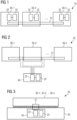
- Figs. 1 and 2 illustrate examples of schematically arranged die arrangements 10, 20 according to embodiments of the invention.
- the die arrangement 10 of Fig. 1 comprises a plurality of dies 30-1, 30-2, 30-n, and a physical interconnection structure 31 extending between and traversing the plurality of dies 30-1, 30-2, 30-n.
- a “die” is a section of semiconducting material on which a logic structure/circuit or a mixed-signal structure/circuit or an analog structure/circuit having a particular function has been established.
- the physical interconnection structure 31 comprises an electrically conducting structure extending between and traversing the plurality of dies 30-1, 30-2, 30-n.
- An “electrically conducting structure” as used herein may relate to a waveguide, a wire, a through-silicon via (TSV) and the like, made of metal or metal alloy.
- TSV through-silicon via
- the physical interconnection structure 31 may alternatively or additionally comprise an optically conducting structure.
- An “optically conducting structure” as used herein may relate to a waveguide or fiber made of a material facilitating conductance of light signals.
- the physical interconnection structure 31 is arranged for imparting unpredictable, yet reproducible properties to a digital signal being carried on the physical interconnection structure 31.
- the physical interconnection structure 31 may be part of a physical unclonable function, PUF, unit.
- a "physical unclonable function" or “PUF” as used herein may typically relate to a digital/mixed signal circuit element being arranged to impart the above-mentioned unpredictable, yet reproducible properties to a digital signal being carried on a physical interconnection structure, and to amplify such properties.
- a "PUF unit” as used herein may relate to a circuit member/structure comprising a PUF and being arranged for imparting, in response to an input (challenge) and using the PUF, the above-mentioned unpredictable, yet reproducible properties, to a corresponding output (response).
- a PUF may turn a digital signal (challenge) into a delayed and/or attenuated digital signal (response), and a change of round-trip delay or differential propagation delays may be monitored.
- Examples of PUF units comprise oscillator PUFs, sum PUFs and arbiter PUFs.
- a PUF unit is less susceptible to disturbances than single RO structures, but requires more chip resources.
- the respective die 30-1, 30-2, 30-n comprises a monitoring logic 32 for monitoring the above-mentioned properties of the digital signal, in particular against characteristic reference data of the digital signal.
- the respective die 30-1, 30-2, 30-n further comprises storage means 33 for the characteristic reference data.
- the respective die 30-1, 30-2, 30-n may be provided with a monitoring logic 32 and corresponding storage means 33 as necessary. For instance, this may not be the case if the die has no security-critical function.
- Monitoring against may relate to observing and evaluating quantities and/or qualities over a period of time, for instance continuously, with reference to (i.e., against) reference quantities and/or qualities.
- Chargeristic reference data may relate to data determined in and representing a non-tampered state of the underlying die arrangement 10, 20. Accordingly, monitored properties of the digital signal corresponding to the characteristic reference data indicate that the underlying die arrangement 10, 20 is in a non-tampered state.
- the characteristic reference data may preferably denote one or more value ranges for particular properties of the digital signal and/or for distinction in terms of criticality of any deviation from the non-tampered state (see below).
- Modification of a topology of the die arrangement 10, 20, be it by separating/desoldering individual dies for reverse engineering, by attachment of additional probes, or by modification of temperature, supply voltage or other global parameters, results in a corresponding modificationof the above-mentioned properties of the digital signal being monitored.
- This entails a possibility of detecting a tampering of the die arrangement 10, 20, in particular by monitoring these properties and comparing them against characteristic reference data of the digital signal. Only few chip resources are needed for tamper detection in the arrangement 10, 20.
- the above die arrangement 10, 20 may be combined with known approaches of tamper detection or tamper hardening. In general, the arrangement 10, 20 further complicates tampering or reverse engineering.
- the respective monitoring logic 32 may be arranged for monitoring semantic properties of the digital signal.
- known communication protocols may be used for semantic monitoring of the digital signal, as these communication protocols define the contents/semantics of the digital signal being carried on the physical interconnection structure 31.
- the digital signal may be captured for subsequent monitoring of cyclic signal patterns or values.
- the respective monitoring logic 32 may alternatively or additionally be arranged for monitoring statistic properties of the digital signal.
- the statistic properties may affect timing properties within a time window. For example, the number of changes from low to high and from high to low within a time window can be determined, or the relation between time periods within the time window in which the signal is high and time periods within the time window in which the signal is low. Furthermore, statistical properties between multiple signals may be determined, e.g., a cross-correlation.
- the respective monitoring logic 32 may alternatively or additionally be arranged for monitoring an eye opening of the digital signal.
- An "eye opening” as used herein may relate to a vertical height, horizontal width and/or a shape/contour of an interior of an eye diagram.
- An eye diagram is generated by superimposing positive and negative pulses of a sampled digital signal such that the superimposed pulses are horizontally centered between their leading and trailing edges.
- the resulting diagram resembles an opening of an eye, and a vertical height, a horizontal width as well as a shape/contour of which provide indications of an average instantaneous attenuation and an average instantaneous delay affecting the sampled digital signal, respectively.
- variations of the instantaneous attenuation and/or instantaneous delay of the digital signal being carried on the physical interconnection structure 31 may be expected, such that the vertical height and/or horizontal width of the interior of the corresponding eye diagram, or simply the eye opening, is varied.
- the physical interconnection structure 31 shown in Fig. 1 forms a ring oscillator, RO, structure.
- the monitoring logic 32 is arranged for monitoring an oscillation frequency of the digital signal being carried on the physical interconnection structure 31.
- the RO structure may comprise a number of logic gates/circuits implementing a feedback loop having a round-trip delay.
- An oscillation frequency of a digital signal being carried on such a structure depends on the above-mentioned random physical factors introduced during manufacturing.
- the RO-structure may be self-oscillating, or merely be excited on demand, which entails power energy savings.
- linear structures on which oscillations or delays may set in are conceivable.
- the characteristic reference data may be machine-learned. For instance, an artificial neural network and known methods of training the same may be used to realize machine learning of the characteristic reference data. This entails a monitoring against automatically learned characteristic reference data without requiring an explicit instance thereof, so that even complex nonlinear properties of the digital data may be monitored and mapped to a non-tampered state or any different state.
- the monitoring logic 32 may, for instance, comprise a tensor processing unit, TPU, for monitoring and evaluating the properties of the digital signal against the machine-learned characteristic reference data. This entails a highly accelerated execution of the machine-learning-based monitoring.
- TPU tensor processing unit
- a “tensor processing unit” or “TPU” is an application-specific integrated circuit, ASIC, developed specifically for accelerating neural network machine learning.
- the characteristic reference data may be determined using hard-coded rules. For instance, heuristics may be used to provide the characteristic reference data. This entails a simple and comprehensible way of determining the characteristic reference data.
- the characteristic reference data may be determined while reducing time-varying environmental factors. It may particularly be recommendable to eliminate an impact of temperature variations on the die arrangement 10, 20. This entails an improved reliability of the monitoring against the characteristic reference data.
- the characteristic reference data may be determined in a provisioning phase during manufacturing of the die arrangement 10, 20. This entails a high amount of flexibility for determining the characteristic reference data.
- Provisioning as used herein may relate to an act, step or state of being prepared before active service or field use.
- the characteristic reference data may be determined in a provisioning phase during commissioning of the die arrangement 10, 20.
- Commissioning as used herein may relate to an act, step or state of configuration, after manufacturing and before active service or field use, at the service site, in field, or a comparable environment.
- the characteristic reference data may be determined during use of the die arrangement 10, 20, i.e. during the above-mentioned active service or field use. This entails a capability of the die arrangement 10, 20 of self-calibration or self-recalibration upon variation of the environmental factors or at the request of the device operator.
- the storage means 33 of the respective die of the plurality of dies 30-1, 30-2, 30-n comprises at least one of a protected memory area and one or more chip fuses.
- a protected memory area may comprise an access-restricted static memory area.
- Storage means 33 based on one or more chip fuses, which are usually put in place for manufacturer configuration of the die, may also be arranged next to the respective die and statically store binary values/digits depending on their presence or absence.
- one or more chip fuses may be used to enable and/or address a particular protected memory area, or permanently store hard-coded characteristic reference data.
- the monitoring logic 32 of the respective die of the plurality of dies 30-1, 30-2, 30-n comprises an internal logic structure of the respective die. This entails that a new die arrangement 20 may be tamper-hardened using the built-in monitoring logic 32.
- an external/separate security IC 40 comprises the monitoring logic 32 in combination with a corresponding storage means 33 for the characteristic reference data.
- This entails that an existing die arrangement 20 may be tamper-hardened using external monitoring logic 32 as implied by the separate security IC 40 in Fig. 2 .
- An external monitoring logic 32 is connected to the physical interconnection structure 31 at interfaces between the plurality of dies 30-1, 30-2, 30-n, see Fig. 2 .
- the monitoring logic 32 is arranged for generating a tamper event upon a detected breach of signal integrity.
- a "tamper event” as used herein may relate to any kind of communication or notification that the properties of the digital signal as monitored by the monitoring logic 32 are not in conformity with the characteristic reference data of the digital signal as stored by its corresponding storage means 33, where non-conformity denotes a breach of signal integrity.
- a breach of signal integrity may, for instance, result from non-conformity of a monitored oscillation frequency, of a monitored eye opening (or corresponding eye opening penalty), or of a monitored PUF-response (e.g. an excessive Hamming distance), and the like.
- a tamper event may comprise setting at least one bit in a particular hardware register or memory location to a defined value, triggering interrupt handling by a processor, or setting an external signal to a defined value, such that a response to such a tamper event may be handled or triggered by another logic member.
- a cryptographic key store may lock access to or delete a stored security key in response to the detection of a tamper event generated by the monitoring logic 32, or security-critical logic functions may be deactivated.
- the monitoring logic 32 may be arranged for logging and/or classifying the tamper event, in particular if the tamper event is passed on to a higher software layer. For instance, depending on a location of tampering, or on a type and/or extent of distortion of an eye diagram, or on an extent of detuning of a RO structure, a tamper event may be classified in terms of its location (e.g. "between dies 1 and 2") and/or criticality. This entails a response at a scale being adequate for and in conformity with the assigned class. The classification may be encoded in the tamper event. This allows classifying the tamper event at a higher level (e.g., in software).
- Figs. 3 and 4 illustrate examples of topologically arranged die arrangements 10, 20 according to embodiments of the invention.
- the die arrangement 20 of Fig. 3 comprises a system-on-chip, SoC, i.e. a monolithic-integrated arrangement of the plurality of dies 30-1, 30-2, 30-n in a common package.
- SoC system-on-chip
- the SoC is arranged and soldered on a PCB 50 using package bumps.
- the die arrangement 20 of Fig. 3 further comprises a discretely arranged security IC 40, which may or may not be seen as belonging to the plurality of dies 30-1, 30-2, 30-n, and which is embedded in a PCB 50.
- the security IC 40 is similar to the one already mentioned in connection with Fig. 2 and may, for instance, comprise a cryptographic key store and be used by the SoC as a cryptographic key store module.
- the physical interconnection structure 31 merely extends between and traverses the plurality of dies 30-1, 30-2, 30-n on the SoC, this entails additional tamper protection by monitoring the integrated die arrangement 20 of the SoC.
- the security IC 40 may be seen as belonging to the plurality of dies 30-1, 30-2, 30-n as already mentioned. This entails additional tamper protection by monitoring the partially integrated die arrangement 20 comprising the plurality of dies 30-1, 30-2, 30-n of the SoC and of the security IC 40.
- the die arrangement 10, 20 of Fig. 4 comprises a hybrid-integrated arrangement of the dies 30-1, 30-2, 30-n in a package 60, denoting a system-in-package, SiP, and including a common substrate 61 arranged and soldered on a PCB 50 using package bumps.
- the die arrangement 20 of Fig. 4 further comprises a silicon interposer 62 having through-silicon vias, TSVs, through which the hybrid-integrated die 30-n is connected to the common substrate 61, as in 2.5D packaging.
- the silicon interposer 62 is arranged and soldered on the common substrate 61 using flip-chip bumps, and the hybrid-integrated die 30-n is arranged and soldered on the silicon interposer 62 using micro bumps.
- the hybrid-integrated die 30-2 of the hybrid-integrated dies 30-1, 30-2, 30-n additionally has TSVs on its part, through which the hybrid-integrated die 30-1 is connected to the common substrate 61, as in 3D packaging.
- the hybrid-integrated dies 30-1, 30-2 are arranged and soldered on the respective underlying TSV-providing component 30-2, 62 using micro bumps.
- the physical interconnection structure 31 extends between and traverses the plurality of dies 30-1, 30-2, 30-n as well as the silicon interposer 62 within the 3D package 60.
- the monitoring logic 32 of the die arrangement 10, 20 is omitted for reasons of improved visibility, but the die arrangement 10, 20 nevertheless comprises an internal logic structure as in Fig. 1 and/or a separate logic structure as in Fig. 2 as the monitoring logic 32. This entails additional tamper protection of the integrated die arrangement 10, 20.
- the topological die arrangement 10, 20 may be monitored in any conceivable die arrangement having any conceivable packaging variant.
- Fig. 5 illustrates a method 70 of an embodiment of the invention, the method 70 being for monitoring a die arrangement 10, 20 of various embodiments.
- the die arrangement 10, 20 underlying the method 70 comprises a plurality of dies 30-1, 30-2, 30-n and a physical interconnection structure 31 extending between and traversing the plurality of dies 30-1, 30-2, 30-n.
- step 71 a digital signal is carried 71 on the physical interconnection structure 31, during which the physical interconnection structure 31 is arranged for imparting unpredictable, yet reproducible properties to the digital signal.
- step 72 the properties of the digital signal are monitored 72.
- the method 70 may be performed for monitoring the die arrangement 10, 20 of various embodiments.
Landscapes
- Engineering & Computer Science (AREA)
- Computer Security & Cryptography (AREA)
- Theoretical Computer Science (AREA)
- Physics & Mathematics (AREA)
- Software Systems (AREA)
- Computer Hardware Design (AREA)
- General Physics & Mathematics (AREA)
- General Engineering & Computer Science (AREA)
- Computer Networks & Wireless Communication (AREA)
- Signal Processing (AREA)
- Mathematical Physics (AREA)
- Semiconductor Integrated Circuits (AREA)
Description
- Various embodiments of the invention relate to semiconductor die arrangements and methods of monitoring the same. Various embodiments relate in particular to such die arrangements and corresponding methods of monitoring which enable detection of tampering of a topological arrangement of a plurality of semiconductor dies to one another.
- In industrial environments, embedded devices like control units, industrial PCs, IoT and edge devices assume important tasks such as, for instance, controlling or monitoring of technical processes, and in doing so often carry out critical functions, in particular with reference to data and information security.
- In addition, the devices are increasingly being networked, e.g., for remote control, or for diagnosis and analysis as a basis for subsequent optimization of a process. In industrial systems, field use of embedded devices often extends over long periods, for instance 10-20 years, or sometimes even 30 or 40 years, during which periods the devices are exposed to ever changing circumstances and potential security attacks.
- Special passive and invasive attacks, such as side-channel attacks/probing, fault injection, depackaging and delayering of integrated circuits, on the hardware of such devices may result in security-critical functions and data being compromised.
- Typical counteractive measures for detection and prevention of such attacks like, for instance, drilling protection (wire meshes), overmoulding of dies/packages using epoxy resin, use of security fuses, use of tamper sensors (detecting security-critical changes in temperature, voltage levels, clock signal properties, light, and/or radiation), monitoring of a current consumption or electromagnetic emission, or use of physical unclonable functions, PUF, typically protect individual integrated circuits or dies only.
- Xie Yang et al. ("Security and Vulnerability implications of 3D ICs", IEEE Transactions on Multi-Scale Computing Systems, IEEE, 27 August 2014) discloses CMOS processors with integrated security primitives involving physical unclonable functions.
US 9,444,618 Bl EP 3 113 409 A1 discloses a silicon integrated circuit comprising a physically unclonable function. - In view of the above, there is a need in the art for detection of tampering of a topological arrangement of semiconductor dies to one another. This equally relates to die arrangements within a same integrated circuit, IC, package, e.g., multi-chip modules, MCM, or system-in-package, SiP, to discrete die arrangements on printed circuit boards, PCB, or to combinations thereof.
- These underlying objects of the invention are each solved by a die arrangement and a method of monitoring the same as defined by the independent claims. Preferred embodiments of the invention are set forth in the dependent claims.
- According to a first aspect, a die arrangement is provided. The die arrangement comprises a plurality of dies; a physical interconnection structure extending between and traversing the plurality of dies, and being arranged for imparting unpredictable, yet reproducible properties to a digital signal being carried on the physical interconnection structure; and a monitoring logic for monitoring the properties of the digital signal.
- The physical interconnection structure may comprise an electrically conducting structure.
- The monitoring logic may be arranged for monitoring the properties of the digital signal against characteristic reference data of the digital signal.
- The monitoring logic may be arranged for monitoring semantic properties of the digital signal.
- The monitoring logic may be arranged for monitoring an eye opening of the digital signal.
- The physical interconnection structure may form a ring oscillator, RO, structure; and the monitoring logic may be arranged for monitoring an oscillation frequency of the digital signal.
- The characteristic reference data may be machine-learned.
- The characteristic reference data may be determined using hard-coded rules.
- The characteristic reference data may be determined while reducing time-varying environmental factors.
- The monitoring logic may comprise storage means for the characteristic reference data.
- The storage means may comprise at least one of a protected memory area and one or more chip fuses.
- The monitoring logic may comprise an internal logic structure of at least one of the plurality of dies.
- The monitoring logic may be arranged for generating a tamper event upon a breach of signal integrity.
- According to a second aspect, a method of monitoring a die arrangement is provided. The underlying die arrangement comprises a plurality of dies and a physical interconnection structure extending between and traversing the plurality of dies. The method comprises a step of carrying a digital signal on the physical interconnection structure, wherein the physical interconnection structure is arranged for imparting unpredictable, yet reproducible properties to the digital signal. The method further comprises a step of monitoring the properties of the digital signal.
- The method is performed for monitoring the die arrangement of various embodiments.
- Embodiments of the invention will be described with reference to the accompanying drawings, in which the same or similar reference numerals designate the same or similar elements.
- Figs. 1 and 2
- illustrate schematic die arrangements according to embodiments of the invention.
- Figs. 3 and 4
- illustrate topological die arrangements according to embodiments of the invention.
- Fig. 5
- illustrates a method of an embodiment of the invention, the method being for monitoring a die arrangement of various embodiments.
- Exemplary embodiments of the invention will now be described with reference to the drawings. While some embodiments will be described in the context of specific fields of application, the embodiments are not limited to this field of application. Further, the features of the various embodiments may be combined with each other unless specifically stated otherwise.
- The drawings are to be regarded as being schematic representations and elements illustrated in the drawings are not necessarily shown to scale. Rather, the various elements are represented such that their function and general purpose become apparent to a person skilled in the art.
-
Figs. 1 and 2 illustrate examples of schematically arranged diearrangements - The die
arrangement 10 ofFig. 1 comprises a plurality of dies 30-1, 30-2, 30-n, and aphysical interconnection structure 31 extending between and traversing the plurality of dies 30-1, 30-2, 30-n. - A "die" is a section of semiconducting material on which a logic structure/circuit or a mixed-signal structure/circuit or an analog structure/circuit having a particular function has been established.
- The
physical interconnection structure 31 comprises an electrically conducting structure extending between and traversing the plurality of dies 30-1, 30-2, 30-n. - An "electrically conducting structure" as used herein may relate to a waveguide, a wire, a through-silicon via (TSV) and the like, made of metal or metal alloy.
- The
physical interconnection structure 31 may alternatively or additionally comprise an optically conducting structure. - An "optically conducting structure" as used herein may relate to a waveguide or fiber made of a material facilitating conductance of light signals.
- The
physical interconnection structure 31 is arranged for imparting unpredictable, yet reproducible properties to a digital signal being carried on thephysical interconnection structure 31. - These properties particularly relate to physical variations occurring naturally during semiconductor manufacture and enabling differentiation between otherwise identical semiconductors. Such random physical factors introduced during manufacturing may, for instance, result in small geometric variations in terms of waveguide lengths, widths, cross-sectional areas, and the like, which in turn result in variations in signal delays, signal attenuation, circuit capacities, and so forth.
- The
physical interconnection structure 31 may be part of a physical unclonable function, PUF, unit. - A "physical unclonable function" or "PUF" as used herein may typically relate to a digital/mixed signal circuit element being arranged to impart the above-mentioned unpredictable, yet reproducible properties to a digital signal being carried on a physical interconnection structure, and to amplify such properties.
- A "PUF unit" as used herein may relate to a circuit member/structure comprising a PUF and being arranged for imparting, in response to an input (challenge) and using the PUF, the above-mentioned unpredictable, yet reproducible properties, to a corresponding output (response). For instance, a PUF may turn a digital signal (challenge) into a delayed and/or attenuated digital signal (response), and a change of round-trip delay or differential propagation delays may be monitored. Examples of PUF units comprise oscillator PUFs, sum PUFs and arbiter PUFs. A PUF unit is less susceptible to disturbances than single RO structures, but requires more chip resources.
- In the non-limiting example of
Fig. 1 , the respective die 30-1, 30-2, 30-n comprises amonitoring logic 32 for monitoring the above-mentioned properties of the digital signal, in particular against characteristic reference data of the digital signal. In this embodiment, the respective die 30-1, 30-2, 30-n further comprises storage means 33 for the characteristic reference data. The respective die 30-1, 30-2, 30-n may be provided with amonitoring logic 32 and corresponding storage means 33 as necessary. For instance, this may not be the case if the die has no security-critical function. - "Monitoring against" as used herein may relate to observing and evaluating quantities and/or qualities over a period of time, for instance continuously, with reference to (i.e., against) reference quantities and/or qualities.
- "Characteristic reference data" as used herein may relate to data determined in and representing a non-tampered state of the
underlying die arrangement underlying die arrangement - Modification of a topology of the
die arrangement die arrangement arrangement above die arrangement arrangement - The
respective monitoring logic 32 may be arranged for monitoring semantic properties of the digital signal. For instance, known communication protocols may be used for semantic monitoring of the digital signal, as these communication protocols define the contents/semantics of the digital signal being carried on thephysical interconnection structure 31. For instance, the digital signal may be captured for subsequent monitoring of cyclic signal patterns or values. - The
respective monitoring logic 32 may alternatively or additionally be arranged for monitoring statistic properties of the digital signal. The statistic properties may affect timing properties within a time window. For example, the number of changes from low to high and from high to low within a time window can be determined, or the relation between time periods within the time window in which the signal is high and time periods within the time window in which the signal is low. Furthermore, statistical properties between multiple signals may be determined, e.g., a cross-correlation. - The
respective monitoring logic 32 may alternatively or additionally be arranged for monitoring an eye opening of the digital signal. - An "eye opening" as used herein may relate to a vertical height, horizontal width and/or a shape/contour of an interior of an eye diagram. An eye diagram is generated by superimposing positive and negative pulses of a sampled digital signal such that the superimposed pulses are horizontally centered between their leading and trailing edges. The resulting diagram resembles an opening of an eye, and a vertical height, a horizontal width as well as a shape/contour of which provide indications of an average instantaneous attenuation and an average instantaneous delay affecting the sampled digital signal, respectively. Upon tampering of the
physical interconnection structure 31, for instance by moving one of the dies 30-1, 30-2, 30-n further away from the others, variations of the instantaneous attenuation and/or instantaneous delay of the digital signal being carried on thephysical interconnection structure 31 may be expected, such that the vertical height and/or horizontal width of the interior of the corresponding eye diagram, or simply the eye opening, is varied. - The
physical interconnection structure 31 shown inFig. 1 forms a ring oscillator, RO, structure. This entails the use of a minimum of chip/interconnection resources. Accordingly, themonitoring logic 32 is arranged for monitoring an oscillation frequency of the digital signal being carried on thephysical interconnection structure 31. For instance, the RO structure may comprise a number of logic gates/circuits implementing a feedback loop having a round-trip delay. An oscillation frequency of a digital signal being carried on such a structure depends on the above-mentioned random physical factors introduced during manufacturing. The RO-structure may be self-oscillating, or merely be excited on demand, which entails power energy savings. Alternatively to a RO structure, also linear structures on which oscillations or delays may set in are conceivable. - The characteristic reference data may be machine-learned. For instance, an artificial neural network and known methods of training the same may be used to realize machine learning of the characteristic reference data. This entails a monitoring against automatically learned characteristic reference data without requiring an explicit instance thereof, so that even complex nonlinear properties of the digital data may be monitored and mapped to a non-tampered state or any different state.
- In such case, the
monitoring logic 32 may, for instance, comprise a tensor processing unit, TPU, for monitoring and evaluating the properties of the digital signal against the machine-learned characteristic reference data. This entails a highly accelerated execution of the machine-learning-based monitoring. - A "tensor processing unit" or "TPU" is an application-specific integrated circuit, ASIC, developed specifically for accelerating neural network machine learning.
- Alternatively or additionally, the characteristic reference data may be determined using hard-coded rules. For instance, heuristics may be used to provide the characteristic reference data. This entails a simple and comprehensible way of determining the characteristic reference data.
- The characteristic reference data may be determined while reducing time-varying environmental factors. It may particularly be recommendable to eliminate an impact of temperature variations on the
die arrangement - The characteristic reference data may be determined in a provisioning phase during manufacturing of the
die arrangement - "Provisioning" as used herein may relate to an act, step or state of being prepared before active service or field use.
- Alternatively or additionally, the characteristic reference data may be determined in a provisioning phase during commissioning of the
die arrangement - "Commissioning" as used herein may relate to an act, step or state of configuration, after manufacturing and before active service or field use, at the service site, in field, or a comparable environment.
- This ensures that the provisioning and the active service or field use are based on comparable environmental factors.
- Alternatively or additionally, the characteristic reference data may be determined during use of the
die arrangement die arrangement - The storage means 33 of the respective die of the plurality of dies 30-1, 30-2, 30-n comprises at least one of a protected memory area and one or more chip fuses. For instance, a protected memory area may comprise an access-restricted static memory area. Storage means 33 based on one or more chip fuses, which are usually put in place for manufacturer configuration of the die, may also be arranged next to the respective die and statically store binary values/digits depending on their presence or absence. For instance, one or more chip fuses may be used to enable and/or address a particular protected memory area, or permanently store hard-coded characteristic reference data.
- In
Fig. 1 , themonitoring logic 32 of the respective die of the plurality of dies 30-1, 30-2, 30-n comprises an internal logic structure of the respective die. This entails that anew die arrangement 20 may be tamper-hardened using the built-inmonitoring logic 32. - By contrast, in the
die arrangement 20 illustrated inFig. 2 , an external/separate security IC 40 comprises themonitoring logic 32 in combination with a corresponding storage means 33 for the characteristic reference data. This entails that an existingdie arrangement 20 may be tamper-hardened usingexternal monitoring logic 32 as implied by theseparate security IC 40 inFig. 2 . Anexternal monitoring logic 32 is connected to thephysical interconnection structure 31 at interfaces between the plurality of dies 30-1, 30-2, 30-n, seeFig. 2 . - In any case, the
monitoring logic 32 is arranged for generating a tamper event upon a detected breach of signal integrity. - A "tamper event" as used herein may relate to any kind of communication or notification that the properties of the digital signal as monitored by the
monitoring logic 32 are not in conformity with the characteristic reference data of the digital signal as stored by its corresponding storage means 33, where non-conformity denotes a breach of signal integrity. - Depending on a type of the
physical interconnection structure 31, a breach of signal integrity may, for instance, result from non-conformity of a monitored oscillation frequency, of a monitored eye opening (or corresponding eye opening penalty), or of a monitored PUF-response (e.g. an excessive Hamming distance), and the like. - For instance, a tamper event may comprise setting at least one bit in a particular hardware register or memory location to a defined value, triggering interrupt handling by a processor, or setting an external signal to a defined value, such that a response to such a tamper event may be handled or triggered by another logic member. For instance, a cryptographic key store may lock access to or delete a stored security key in response to the detection of a tamper event generated by the
monitoring logic 32, or security-critical logic functions may be deactivated. - The
monitoring logic 32 may be arranged for logging and/or classifying the tamper event, in particular if the tamper event is passed on to a higher software layer. For instance, depending on a location of tampering, or on a type and/or extent of distortion of an eye diagram, or on an extent of detuning of a RO structure, a tamper event may be classified in terms of its location (e.g. "between dies 1 and 2") and/or criticality. This entails a response at a scale being adequate for and in conformity with the assigned class. The classification may be encoded in the tamper event. This allows classifying the tamper event at a higher level (e.g., in software). -
Figs. 3 and4 illustrate examples of topologically arranged diearrangements - The
die arrangement 20 ofFig. 3 comprises a system-on-chip, SoC, i.e. a monolithic-integrated arrangement of the plurality of dies 30-1, 30-2, 30-n in a common package. According to the example ofFig. 3 , the SoC is arranged and soldered on aPCB 50 using package bumps. - The
die arrangement 20 ofFig. 3 further comprises a discretely arrangedsecurity IC 40, which may or may not be seen as belonging to the plurality of dies 30-1, 30-2, 30-n, and which is embedded in aPCB 50. Thesecurity IC 40 is similar to the one already mentioned in connection withFig. 2 and may, for instance, comprise a cryptographic key store and be used by the SoC as a cryptographic key store module. - If the
physical interconnection structure 31 merely extends between and traverses the plurality of dies 30-1, 30-2, 30-n on the SoC, this entails additional tamper protection by monitoring the integrated diearrangement 20 of the SoC. - If the
physical interconnection structure 31 extends between and traverses the plurality of dies 30-1, 30-2, 30-n including thesecurity IC 40, as depicted inFig. 3 , then thesecurity IC 40 may be seen as belonging to the plurality of dies 30-1, 30-2, 30-n as already mentioned. This entails additional tamper protection by monitoring the partially integrated diearrangement 20 comprising the plurality of dies 30-1, 30-2, 30-n of the SoC and of thesecurity IC 40. - The
die arrangement Fig. 4 comprises a hybrid-integrated arrangement of the dies 30-1, 30-2, 30-n in apackage 60, denoting a system-in-package, SiP, and including acommon substrate 61 arranged and soldered on aPCB 50 using package bumps. - Unlike 2D packaging, in which the hybrid-integrated dies 30-1, 30-2, 30-n would be directly connected to the
common substrate 61, thedie arrangement 20 ofFig. 4 further comprises asilicon interposer 62 having through-silicon vias, TSVs, through which the hybrid-integrated die 30-n is connected to thecommon substrate 61, as in 2.5D packaging. Thesilicon interposer 62 is arranged and soldered on thecommon substrate 61 using flip-chip bumps, and the hybrid-integrated die 30-n is arranged and soldered on thesilicon interposer 62 using micro bumps. - In the
die arrangement Fig. 4 , the hybrid-integrated die 30-2 of the hybrid-integrated dies 30-1, 30-2, 30-n additionally has TSVs on its part, through which the hybrid-integrated die 30-1 is connected to thecommon substrate 61, as in 3D packaging. The hybrid-integrated dies 30-1, 30-2 are arranged and soldered on the respective underlying TSV-providing component 30-2, 62 using micro bumps. - In the embodiment of
Fig. 4 , thephysical interconnection structure 31 extends between and traverses the plurality of dies 30-1, 30-2, 30-n as well as thesilicon interposer 62 within the3D package 60. - In
Fig. 4 , themonitoring logic 32 of thedie arrangement die arrangement Fig. 1 and/or a separate logic structure as inFig. 2 as themonitoring logic 32. This entails additional tamper protection of the integrated diearrangement - In summary, the topological die
arrangement -
Fig. 5 illustrates amethod 70 of an embodiment of the invention, themethod 70 being for monitoring adie arrangement - The
die arrangement method 70 comprises a plurality of dies 30-1, 30-2, 30-n and aphysical interconnection structure 31 extending between and traversing the plurality of dies 30-1, 30-2, 30-n. - In
step 71, a digital signal is carried 71 on thephysical interconnection structure 31, during which thephysical interconnection structure 31 is arranged for imparting unpredictable, yet reproducible properties to the digital signal. - In step 72, the properties of the digital signal are monitored 72.
- The
method 70 may be performed for monitoring thedie arrangement - The technical effects and advantages described above in relation with the die arrangement of various embodiments equally apply to the corresponding method for monitoring the die arrangement having corresponding features.
- While die arrangements and methods of monitoring the same of various embodiments have been described, those skilled in the art will appreciate that the present invention is not so limited and that the present invention may be carried out in other ways than those specifically set forth herein without departing from essential characteristics of the invention. The present embodiments are therefore to be considered in all respects as illustrative and not restrictive, and all changes coming within the meaning and equivalency range of the appended claims are intended to be embraced therein.
Claims (13)
- A die arrangement (10, 20), comprisinga plurality of dies (30-1, 30-2, 30-n);a physical interconnection structure (31) extending between and traversing the plurality of dies (30-1, 30-2, 30-n), and being arranged for imparting unpredictable, yet reproducible properties to a digital signal being carried on the physical interconnection structure (31); anda monitoring logic (32) for monitoring the properties of the digital signal,the monitoring logic (32) being arranged for monitoring the properties of the digital signal against characteristic reference data of the digital signal, whereinthe die arrangement (10, 20) comprises storage means (33) comprising at least one of a protected memory area for the characteristic reference data and wherein non-conformity of the digital signal as monitored by the monitoring logic (32) with the characteristic reference data denotes a breach of signal integrity of the digital signal.
- The die arrangement (10, 20) of claim 1,
the physical interconnection structure (31) comprising an electrically conducting structure. - The die arrangement (10, 20) of any one of the preceding claims,
the monitoring logic (32) being arranged for monitoring semantics properties of the digital signal. - The die arrangement (10, 20) of any one of the preceding claims,
the monitoring logic (32) being arranged for monitoring an eye opening of the digital signal. - The die arrangement (10, 20) of any one of the preceding claims,the physical interconnection structure (31) forming a ring oscillator, RO, structure; andthe monitoring logic (32) being arranged for monitoring an oscillation frequency of the digital signal.
- The die arrangement (10, 20) of any one of the preceding claims,
the characteristic reference data being machine-learned. - The die arrangement (10, 20) of any one of the preceding claims,
the characteristic reference data being determined using hard-coded rules. - The die arrangement (10, 20) of any one of the preceding claims,
the characteristic reference data being determined while reducing time-varying environmental factors. - The die arrangement (10, 20) of any one of claims 3 to 8, the monitoring logic (32) comprising the storage means (33) for the characteristic reference data.
- The die arrangement (10, 20) of any one of the preceding claims,
the storage means (33) comprising at least one of a protected memory area and one or more chip fuses. - The die arrangement (10, 20) of any one of the preceding claims,
the monitoring logic (32) comprising an internal logic structure of at least one of the plurality of dies (30-1, 30-2, 30-n). - The die arrangement (10, 20) of any one of the preceding claims,
the monitoring logic (32) being arranged for generating a tamper event upon a breach of signal integrity. - A method (70) of monitoring a die arrangement (10, 20), the die arrangement (10, 20) comprising a plurality of dies (30-1, 30-2, 30-n) and a physical interconnection structure (31) extending between and traversing the plurality of dies (30-1, 30-2, 30-n), the method (70) comprisingcarrying (71) a digital signal on the physical interconnection structure (31), the physical interconnection structure (31) being arranged for imparting unpredictable, yet reproducible properties to the digital signal; andmonitoring (72) the properties of the digital signal,the method (70) being performed for monitoring of the die arrangement (10, 20) of any one of claims 1 - 12.
Priority Applications (5)
| Application Number | Priority Date | Filing Date | Title |
|---|---|---|---|
| EP19154376.8A EP3690867B1 (en) | 2019-01-30 | 2019-01-30 | Fingerprinting of semiconductor die arrangements |
| EP19821041.1A EP3891720A1 (en) | 2019-01-30 | 2019-12-04 | Fingerprinting of semiconductor die arrangements |
| US17/425,808 US20220179950A1 (en) | 2019-01-30 | 2019-12-04 | Fingerprinting of semiconductor die arrangements |
| PCT/EP2019/083622 WO2020156708A1 (en) | 2019-01-30 | 2019-12-04 | Fingerprinting of semiconductor die arrangements |
| CN201980090899.1A CN113383376A (en) | 2019-01-30 | 2019-12-04 | Fingerprinting of semiconductor die arrangements |
Applications Claiming Priority (1)
| Application Number | Priority Date | Filing Date | Title |
|---|---|---|---|
| EP19154376.8A EP3690867B1 (en) | 2019-01-30 | 2019-01-30 | Fingerprinting of semiconductor die arrangements |
Publications (2)
| Publication Number | Publication Date |
|---|---|
| EP3690867A1 EP3690867A1 (en) | 2020-08-05 |
| EP3690867B1 true EP3690867B1 (en) | 2025-06-11 |
Family
ID=65243473
Family Applications (2)
| Application Number | Title | Priority Date | Filing Date |
|---|---|---|---|
| EP19154376.8A Active EP3690867B1 (en) | 2019-01-30 | 2019-01-30 | Fingerprinting of semiconductor die arrangements |
| EP19821041.1A Withdrawn EP3891720A1 (en) | 2019-01-30 | 2019-12-04 | Fingerprinting of semiconductor die arrangements |
Family Applications After (1)
| Application Number | Title | Priority Date | Filing Date |
|---|---|---|---|
| EP19821041.1A Withdrawn EP3891720A1 (en) | 2019-01-30 | 2019-12-04 | Fingerprinting of semiconductor die arrangements |
Country Status (4)
| Country | Link |
|---|---|
| US (1) | US20220179950A1 (en) |
| EP (2) | EP3690867B1 (en) |
| CN (1) | CN113383376A (en) |
| WO (1) | WO2020156708A1 (en) |
Families Citing this family (5)
| Publication number | Priority date | Publication date | Assignee | Title |
|---|---|---|---|---|
| US11985259B2 (en) * | 2021-06-24 | 2024-05-14 | Raytheon Company | Unified multi-die physical unclonable function |
| US12309299B2 (en) * | 2021-09-22 | 2025-05-20 | Intel Corporation | Method, system and apparatus for protection of multi-die structures |
| US20230109011A1 (en) * | 2021-10-04 | 2023-04-06 | Hewlett-Packard Development Company, L.P. | Placing a device in secure mode |
| US12314451B2 (en) * | 2022-01-21 | 2025-05-27 | Nvidia Corporation | Selective communication interfaces for programmable parts |
| WO2024205742A1 (en) * | 2023-03-27 | 2024-10-03 | PseudolithIC, Inc. | Built in self-test of heterogeneous integrated radio frequency chiplets |
Citations (5)
| Publication number | Priority date | Publication date | Assignee | Title |
|---|---|---|---|---|
| WO2011018414A2 (en) * | 2009-08-14 | 2011-02-17 | Intrinsic Id B.V. | Physically unclonable function with tamper prevention and anti-aging system |
| US20110055649A1 (en) * | 2009-08-25 | 2011-03-03 | Farinaz Koushanfar | Testing security of mapping functions |
| EP3032421A1 (en) * | 2013-07-26 | 2016-06-15 | ICTK Co. Ltd. | Device and method for testing randomness |
| US9444618B1 (en) * | 2013-04-22 | 2016-09-13 | Xilinx, Inc. | Defense against attacks on ring oscillator-based physically unclonable functions |
| EP3113409A1 (en) * | 2015-07-01 | 2017-01-04 | Secure-IC SAS | Embedded test circuit for physically unclonable function |
Family Cites Families (13)
| Publication number | Priority date | Publication date | Assignee | Title |
|---|---|---|---|---|
| GB2481738B (en) * | 2009-04-30 | 2013-10-16 | Hewlett Packard Development Co | Die connection monitoring system and method |
| US8296578B1 (en) * | 2009-08-03 | 2012-10-23 | Xilinx, Inc. | Method and apparatus for communicating data between stacked integrated circuits |
| US9059189B2 (en) * | 2011-03-02 | 2015-06-16 | Nokomis, Inc | Integrated circuit with electromagnetic energy anomaly detection and processing |
| US8928347B2 (en) * | 2012-09-28 | 2015-01-06 | Intel Corporation | Integrated circuits having accessible and inaccessible physically unclonable functions |
| US9366718B2 (en) * | 2013-09-12 | 2016-06-14 | Cisco Technology Inc. | Detection of disassembly of multi-die chip assemblies |
| WO2016180977A1 (en) * | 2015-05-13 | 2016-11-17 | Nagravision S.A. | Integrated circuit chip protection against physical and/or electrical alterations |
| FR3051599A1 (en) * | 2016-05-17 | 2017-11-24 | Stmicroelectronics Rousset | PROTECTION OF AN INTEGRATED CIRCUIT |
| EP3327756B1 (en) * | 2016-11-24 | 2019-11-06 | Melexis Technologies NV | Die edge integrity monitoring system and corresponding method |
| US10445278B2 (en) * | 2016-12-28 | 2019-10-15 | Intel Corporation | Interface bridge between integrated circuit die |
| US10547461B2 (en) * | 2017-03-07 | 2020-01-28 | Nxp B.V. | Method and apparatus for binding stacked die using a physically unclonable function |
| US10891366B1 (en) * | 2017-08-18 | 2021-01-12 | Jonetix Corporation | Secure hardware signature and related methods and applications |
| BR112022004110A2 (en) * | 2019-09-06 | 2022-05-31 | Lexmark Int Inc | A sensor array for reading a magnetic pouf |
| US12309299B2 (en) * | 2021-09-22 | 2025-05-20 | Intel Corporation | Method, system and apparatus for protection of multi-die structures |
-
2019
- 2019-01-30 EP EP19154376.8A patent/EP3690867B1/en active Active
- 2019-12-04 US US17/425,808 patent/US20220179950A1/en not_active Abandoned
- 2019-12-04 EP EP19821041.1A patent/EP3891720A1/en not_active Withdrawn
- 2019-12-04 CN CN201980090899.1A patent/CN113383376A/en active Pending
- 2019-12-04 WO PCT/EP2019/083622 patent/WO2020156708A1/en not_active Ceased
Patent Citations (5)
| Publication number | Priority date | Publication date | Assignee | Title |
|---|---|---|---|---|
| WO2011018414A2 (en) * | 2009-08-14 | 2011-02-17 | Intrinsic Id B.V. | Physically unclonable function with tamper prevention and anti-aging system |
| US20110055649A1 (en) * | 2009-08-25 | 2011-03-03 | Farinaz Koushanfar | Testing security of mapping functions |
| US9444618B1 (en) * | 2013-04-22 | 2016-09-13 | Xilinx, Inc. | Defense against attacks on ring oscillator-based physically unclonable functions |
| EP3032421A1 (en) * | 2013-07-26 | 2016-06-15 | ICTK Co. Ltd. | Device and method for testing randomness |
| EP3113409A1 (en) * | 2015-07-01 | 2017-01-04 | Secure-IC SAS | Embedded test circuit for physically unclonable function |
Also Published As
| Publication number | Publication date |
|---|---|
| US20220179950A1 (en) | 2022-06-09 |
| EP3690867A1 (en) | 2020-08-05 |
| EP3891720A1 (en) | 2021-10-13 |
| WO2020156708A1 (en) | 2020-08-06 |
| CN113383376A (en) | 2021-09-10 |
Similar Documents
| Publication | Publication Date | Title |
|---|---|---|
| US20220179950A1 (en) | Fingerprinting of semiconductor die arrangements | |
| Li et al. | At-speed delay characterization for IC authentication and Trojan horse detection | |
| EP2573716B1 (en) | Secure device anti-tampering circuit | |
| US10289840B2 (en) | Integrated circuit with tamper protection and method therefor | |
| Manich et al. | Detection of probing attempts in secure ICs | |
| Deng et al. | Novel design strategy toward a2 trojan detection based on built-in acceleration structure | |
| Vashistha et al. | Is backside the new backdoor in modern socs? | |
| Roshanisefat et al. | Benchmarking the capabilities and limitations of sat solvers in defeating obfuscation schemes | |
| Wang et al. | Hardware trojan detection and high-precision localization in noc-based mpsoc using machine learning | |
| CN111208415A (en) | Distributed ring oscillator network layout filling hardware Trojan horse detection method and circuit | |
| Qin et al. | Sensitivity analysis of ring oscillator based hardware Trojan detection | |
| Deepthi | Hardware trojan detection using ring oscillator | |
| EP3044722B1 (en) | Detection of disassembly of multi-die chip assemblies | |
| Matsumoto et al. | Secure cryptographic unit as root-of-trust for IoT era | |
| Köylü et al. | Exploiting PUF variation to detect fault injection attacks | |
| US11481522B2 (en) | Circuit configured to monitor a sensitive payload for attack detection | |
| Rajendran et al. | Sok: Physical and logic testing techniques for hardware trojan detection | |
| Forte et al. | Supply-chain security for cyberinfrastructure [Guest editors' introduction] | |
| Su et al. | Golden-chip-free hardware trojan detection through thermal radiation comparison in vulnerable areas | |
| Moghadas et al. | ROPAD: enhancing the digital ring oscillator probing attempt detector for protecting irregular data buses | |
| Giechaskiel et al. | Long-Wire Leakage: The Threat of Crosstalk. | |
| Mondal et al. | XOR based methodology to detect hardware trojan utilizing the transition probability | |
| Yi et al. | Practical silicon-backside-protection method for abnormally detection | |
| US20250132270A1 (en) | Chip package with tamper prevention | |
| Thajte et al. | Pulsed ElectroMagnetic Fault Injection Attack on a Time Measurement-based Arbiter-PUF |
Legal Events
| Date | Code | Title | Description |
|---|---|---|---|
| STAA | Information on the status of an ep patent application or granted ep patent |
Free format text: STATUS: EXAMINATION IS IN PROGRESS |
|
| PUAI | Public reference made under article 153(3) epc to a published international application that has entered the european phase |
Free format text: ORIGINAL CODE: 0009012 |
|
| 17P | Request for examination filed |
Effective date: 20191105 |
|
| AK | Designated contracting states |
Kind code of ref document: A1 Designated state(s): AL AT BE BG CH CY CZ DE DK EE ES FI FR GB GR HR HU IE IS IT LI LT LU LV MC MK MT NL NO PL PT RO RS SE SI SK SM TR |
|
| AX | Request for extension of the european patent |
Extension state: BA ME |
|
| GRAP | Despatch of communication of intention to grant a patent |
Free format text: ORIGINAL CODE: EPIDOSNIGR1 |
|
| STAA | Information on the status of an ep patent application or granted ep patent |
Free format text: STATUS: GRANT OF PATENT IS INTENDED |
|
| RIC1 | Information provided on ipc code assigned before grant |
Ipc: H04L 9/32 20060101ALI20250214BHEP Ipc: G09C 1/00 20060101AFI20250214BHEP |
|
| INTG | Intention to grant announced |
Effective date: 20250303 |
|
| GRAS | Grant fee paid |
Free format text: ORIGINAL CODE: EPIDOSNIGR3 |
|
| GRAA | (expected) grant |
Free format text: ORIGINAL CODE: 0009210 |
|
| STAA | Information on the status of an ep patent application or granted ep patent |
Free format text: STATUS: THE PATENT HAS BEEN GRANTED |
|
| AK | Designated contracting states |
Kind code of ref document: B1 Designated state(s): AL AT BE BG CH CY CZ DE DK EE ES FI FR GB GR HR HU IE IS IT LI LT LU LV MC MK MT NL NO PL PT RO RS SE SI SK SM TR |
|
| REG | Reference to a national code |
Ref country code: GB Ref legal event code: FG4D |
|
| REG | Reference to a national code |
Ref country code: CH Ref legal event code: EP |
|
| REG | Reference to a national code |
Ref country code: IE Ref legal event code: FG4D |
|
| REG | Reference to a national code |
Ref country code: DE Ref legal event code: R096 Ref document number: 602019070967 Country of ref document: DE |
|
| PG25 | Lapsed in a contracting state [announced via postgrant information from national office to epo] |
Ref country code: FI Free format text: LAPSE BECAUSE OF FAILURE TO SUBMIT A TRANSLATION OF THE DESCRIPTION OR TO PAY THE FEE WITHIN THE PRESCRIBED TIME-LIMIT Effective date: 20250611 Ref country code: ES Free format text: LAPSE BECAUSE OF FAILURE TO SUBMIT A TRANSLATION OF THE DESCRIPTION OR TO PAY THE FEE WITHIN THE PRESCRIBED TIME-LIMIT Effective date: 20250611 |
|
| REG | Reference to a national code |
Ref country code: LT Ref legal event code: MG9D |
|
| PG25 | Lapsed in a contracting state [announced via postgrant information from national office to epo] |
Ref country code: GR Free format text: LAPSE BECAUSE OF FAILURE TO SUBMIT A TRANSLATION OF THE DESCRIPTION OR TO PAY THE FEE WITHIN THE PRESCRIBED TIME-LIMIT Effective date: 20250912 Ref country code: NO Free format text: LAPSE BECAUSE OF FAILURE TO SUBMIT A TRANSLATION OF THE DESCRIPTION OR TO PAY THE FEE WITHIN THE PRESCRIBED TIME-LIMIT Effective date: 20250911 |
|
| REG | Reference to a national code |
Ref country code: NL Ref legal event code: MP Effective date: 20250611 |
|
| PG25 | Lapsed in a contracting state [announced via postgrant information from national office to epo] |
Ref country code: BG Free format text: LAPSE BECAUSE OF FAILURE TO SUBMIT A TRANSLATION OF THE DESCRIPTION OR TO PAY THE FEE WITHIN THE PRESCRIBED TIME-LIMIT Effective date: 20250611 |
|
| PG25 | Lapsed in a contracting state [announced via postgrant information from national office to epo] |
Ref country code: HR Free format text: LAPSE BECAUSE OF FAILURE TO SUBMIT A TRANSLATION OF THE DESCRIPTION OR TO PAY THE FEE WITHIN THE PRESCRIBED TIME-LIMIT Effective date: 20250611 |
|
| PG25 | Lapsed in a contracting state [announced via postgrant information from national office to epo] |
Ref country code: RS Free format text: LAPSE BECAUSE OF FAILURE TO SUBMIT A TRANSLATION OF THE DESCRIPTION OR TO PAY THE FEE WITHIN THE PRESCRIBED TIME-LIMIT Effective date: 20250911 |
|
| PG25 | Lapsed in a contracting state [announced via postgrant information from national office to epo] |
Ref country code: LV Free format text: LAPSE BECAUSE OF FAILURE TO SUBMIT A TRANSLATION OF THE DESCRIPTION OR TO PAY THE FEE WITHIN THE PRESCRIBED TIME-LIMIT Effective date: 20250611 |
|
| PG25 | Lapsed in a contracting state [announced via postgrant information from national office to epo] |
Ref country code: NL Free format text: LAPSE BECAUSE OF FAILURE TO SUBMIT A TRANSLATION OF THE DESCRIPTION OR TO PAY THE FEE WITHIN THE PRESCRIBED TIME-LIMIT Effective date: 20250611 |
|
| PG25 | Lapsed in a contracting state [announced via postgrant information from national office to epo] |
Ref country code: PT Free format text: LAPSE BECAUSE OF FAILURE TO SUBMIT A TRANSLATION OF THE DESCRIPTION OR TO PAY THE FEE WITHIN THE PRESCRIBED TIME-LIMIT Effective date: 20251013 |
|
| REG | Reference to a national code |
Ref country code: AT Ref legal event code: MK05 Ref document number: 1802911 Country of ref document: AT Kind code of ref document: T Effective date: 20250611 |
|
| PG25 | Lapsed in a contracting state [announced via postgrant information from national office to epo] |
Ref country code: IS Free format text: LAPSE BECAUSE OF FAILURE TO SUBMIT A TRANSLATION OF THE DESCRIPTION OR TO PAY THE FEE WITHIN THE PRESCRIBED TIME-LIMIT Effective date: 20251011 |
|
| PG25 | Lapsed in a contracting state [announced via postgrant information from national office to epo] |
Ref country code: AT Free format text: LAPSE BECAUSE OF FAILURE TO SUBMIT A TRANSLATION OF THE DESCRIPTION OR TO PAY THE FEE WITHIN THE PRESCRIBED TIME-LIMIT Effective date: 20250611 Ref country code: SM Free format text: LAPSE BECAUSE OF FAILURE TO SUBMIT A TRANSLATION OF THE DESCRIPTION OR TO PAY THE FEE WITHIN THE PRESCRIBED TIME-LIMIT Effective date: 20250611 |
|
| PG25 | Lapsed in a contracting state [announced via postgrant information from national office to epo] |
Ref country code: CZ Free format text: LAPSE BECAUSE OF FAILURE TO SUBMIT A TRANSLATION OF THE DESCRIPTION OR TO PAY THE FEE WITHIN THE PRESCRIBED TIME-LIMIT Effective date: 20250611 |
|
| PG25 | Lapsed in a contracting state [announced via postgrant information from national office to epo] |
Ref country code: PL Free format text: LAPSE BECAUSE OF FAILURE TO SUBMIT A TRANSLATION OF THE DESCRIPTION OR TO PAY THE FEE WITHIN THE PRESCRIBED TIME-LIMIT Effective date: 20250611 |
|
| PG25 | Lapsed in a contracting state [announced via postgrant information from national office to epo] |
Ref country code: EE Free format text: LAPSE BECAUSE OF FAILURE TO SUBMIT A TRANSLATION OF THE DESCRIPTION OR TO PAY THE FEE WITHIN THE PRESCRIBED TIME-LIMIT Effective date: 20250611 |
|
| PG25 | Lapsed in a contracting state [announced via postgrant information from national office to epo] |
Ref country code: SK Free format text: LAPSE BECAUSE OF FAILURE TO SUBMIT A TRANSLATION OF THE DESCRIPTION OR TO PAY THE FEE WITHIN THE PRESCRIBED TIME-LIMIT Effective date: 20250611 Ref country code: RO Free format text: LAPSE BECAUSE OF FAILURE TO SUBMIT A TRANSLATION OF THE DESCRIPTION OR TO PAY THE FEE WITHIN THE PRESCRIBED TIME-LIMIT Effective date: 20250611 |
|
| REG | Reference to a national code |
Ref country code: DE Ref legal event code: R097 Ref document number: 602019070967 Country of ref document: DE |
|
| PG25 | Lapsed in a contracting state [announced via postgrant information from national office to epo] |
Ref country code: DK Free format text: LAPSE BECAUSE OF FAILURE TO SUBMIT A TRANSLATION OF THE DESCRIPTION OR TO PAY THE FEE WITHIN THE PRESCRIBED TIME-LIMIT Effective date: 20250611 |
|
| PG25 | Lapsed in a contracting state [announced via postgrant information from national office to epo] |
Ref country code: IT Free format text: LAPSE BECAUSE OF FAILURE TO SUBMIT A TRANSLATION OF THE DESCRIPTION OR TO PAY THE FEE WITHIN THE PRESCRIBED TIME-LIMIT Effective date: 20250611 |
|
| PLBE | No opposition filed within time limit |
Free format text: ORIGINAL CODE: 0009261 |
|
| STAA | Information on the status of an ep patent application or granted ep patent |
Free format text: STATUS: NO OPPOSITION FILED WITHIN TIME LIMIT |
|
| REG | Reference to a national code |
Ref country code: CH Ref legal event code: L10 Free format text: ST27 STATUS EVENT CODE: U-0-0-L10-L00 (AS PROVIDED BY THE NATIONAL OFFICE) Effective date: 20260423 |