EP3690615A1 - Pointing device - Google Patents
Pointing device Download PDFInfo
- Publication number
- EP3690615A1 EP3690615A1 EP18861050.5A EP18861050A EP3690615A1 EP 3690615 A1 EP3690615 A1 EP 3690615A1 EP 18861050 A EP18861050 A EP 18861050A EP 3690615 A1 EP3690615 A1 EP 3690615A1
- Authority
- EP
- European Patent Office
- Prior art keywords
- electrode
- signal
- stylus
- control circuit
- output
- Prior art date
- Legal status (The legal status is an assumption and is not a legal conclusion. Google has not performed a legal analysis and makes no representation as to the accuracy of the status listed.)
- Granted
Links
Images




Classifications
-
- G—PHYSICS
- G06—COMPUTING OR CALCULATING; COUNTING
- G06F—ELECTRIC DIGITAL DATA PROCESSING
- G06F3/00—Input arrangements for transferring data to be processed into a form capable of being handled by the computer; Output arrangements for transferring data from processing unit to output unit, e.g. interface arrangements
- G06F3/01—Input arrangements or combined input and output arrangements for interaction between user and computer
- G06F3/03—Arrangements for converting the position or the displacement of a member into a coded form
- G06F3/041—Digitisers, e.g. for touch screens or touch pads, characterised by the transducing means
- G06F3/044—Digitisers, e.g. for touch screens or touch pads, characterised by the transducing means by capacitive means
- G06F3/0442—Digitisers, e.g. for touch screens or touch pads, characterised by the transducing means by capacitive means using active external devices, e.g. active pens, for transmitting changes in electrical potential to be received by the digitiser
-
- G—PHYSICS
- G06—COMPUTING OR CALCULATING; COUNTING
- G06F—ELECTRIC DIGITAL DATA PROCESSING
- G06F3/00—Input arrangements for transferring data to be processed into a form capable of being handled by the computer; Output arrangements for transferring data from processing unit to output unit, e.g. interface arrangements
- G06F3/01—Input arrangements or combined input and output arrangements for interaction between user and computer
- G06F3/03—Arrangements for converting the position or the displacement of a member into a coded form
- G06F3/033—Pointing devices displaced or positioned by the user, e.g. mice, trackballs, pens or joysticks; Accessories therefor
- G06F3/0354—Pointing devices displaced or positioned by the user, e.g. mice, trackballs, pens or joysticks; Accessories therefor with detection of two-dimensional [2D] relative movements between the device, or an operating part thereof, and a plane or surface, e.g. 2D mice, trackballs, pens or pucks
- G06F3/03545—Pens or stylus
-
- G—PHYSICS
- G06—COMPUTING OR CALCULATING; COUNTING
- G06F—ELECTRIC DIGITAL DATA PROCESSING
- G06F3/00—Input arrangements for transferring data to be processed into a form capable of being handled by the computer; Output arrangements for transferring data from processing unit to output unit, e.g. interface arrangements
- G06F3/01—Input arrangements or combined input and output arrangements for interaction between user and computer
- G06F3/03—Arrangements for converting the position or the displacement of a member into a coded form
- G06F3/041—Digitisers, e.g. for touch screens or touch pads, characterised by the transducing means
- G06F3/0416—Control or interface arrangements specially adapted for digitisers
- G06F3/04162—Control or interface arrangements specially adapted for digitisers for exchanging data with external devices, e.g. smart pens, via the digitiser sensing hardware
Definitions
- the present invention relates to a position indicator that operates by a capacitance method to interact capacitively with a sensor of a position detection apparatus.
- the position indicator having a signal transmission circuit that transmits a signal via a conductive stylus to a sensor of a position detection apparatus through capacitive coupling.
- the position detection apparatus receives a signal from the active capacitive pen via the sensor that includes multiple sensor conductors.
- the position detection apparatus detects the position on the sensor that is pointed by a pen tip of a stylus of the active capacitive pen in accordance with a signal level on the sensor conductors having received the signal.
- the position detection apparatus can detect the position pointed by the pen tip of the stylus with substantial accuracy.
- One problem is that when the axial center direction of the stylus is tilted relative to the input surface of the sensor, the position detection apparatus cannot accurately detect the position pointed by the pen tip of the stylus.
- FIG. 11 is a view explaining a relationship between the tilt angles of the axial center direction of the stylus of the position indicator relative to the input surface of the sensor on one hand and the signal levels of the signal received by the sensor of the position detection apparatus from the position indicator on the other hand.
- FIG. 11 illustrates the signal levels of the signal received by multiple conductors (conductors Xi-2, Xi-1, Xi, Xi+1, and Xi+2 in the example of FIG. 11 ) arranged in an X-axis direction (e.g., crosswise direction) of the sensor.
- the sensor has multiple conductors arranged likewise in a Y-axis direction as well. Similar signal levels also appear on these conductors arranged in the Y-axis direction.
- FIG. 11(A) indicates the signal levels of the signal received by the conductors Xi-2, Xi-1, Xi, Xi+1, and Xi+2 in a case where the axial center direction of a stylus 100 of the position indicator is perpendicular to the input surface of the sensor of the position detection apparatus and where the stylus 100 (i.e., its pen tip) is directly above the conductor Xi.
- the signal from the stylus 100 is transmitted substantially from the tip of the stylus to the sensor.
- the signal level of the signal received by each of the conductors Xi-2, Xi-1, Xi, Xi+1 and Xi+2 is highest on the conductor Xi at the center and is progressively lower on the conductors Xi-2 and Xi-1 to the left of the conductor Xi and on the conductors Xi+1 and Xi+2 to the right thereof in a symmetrical manner, as illustrated in FIG. 11(A) .
- the position detection apparatus detects the position on the sensor pointed by the stylus 100 by performing calculations using the signal levels of the signal received by the conductors Xi-2, Xi-1, Xi, Xi+1, and Xi+2. In the case of FIG. 11(A) , a position P0 (X coordinate) pointed by the stylus 100 is detected correctly as the position of the conductor Xi.
- FIG. 11(B) depicts the signal levels of the signal received by the conductors Xi-2, Xi-1, Xi, Xi+1, and Xi+2 in a case where the pen tip of the stylus 100 of the position indicator is directly above the conductor Xi but where the stylus 100 is tilted relative to the input surface of the sensor of the position detection apparatus at a predetermined angle ⁇ ( ⁇ ⁇ 90 degrees) in the X-axis direction.
- the signal from the stylus 100 is transmitted to the sensor not only from the stylus tip but also effectively from a stylus portion close to the sensor in keeping with the tilt.
- the signal level of the signal received by each of the conductors Xi-2, Xi-1, Xi, Xi+1 and Xi+2 is highest on the conductor Xi at the center and is progressively lower on the conductors Xi-2 and Xi-1 to the left of the conductor Xi and on the conductors Xi+1 and Xi+2 to the right thereof in an asymmetrical manner in keeping with the tilt of the stylus 100, as depicted in FIG. 11(B) .
- the position detection apparatus detects the position pointed by the stylus 100 by performing calculations using the signal levels of the signal received by the conductors Xi-2, Xi-1, Xi, Xi+1, and Xi+2 in the state in FIG. 11(B) . Consequently, the position pointed by the stylus 100 is shifted to a position P1 in the direction in which the stylus 100 is tilted by the amount reflecting the tilt angle. The position P1 deviates by ⁇ P from the position P0 pointed by the tip of the stylus 100.
- the present invention provides a position indicator including a pen-like housing, a first electrode, a second electrode, and a signal transmission control circuit, the first electrode and the second electrode being arranged at one end of the housing in an axial center direction thereof, the second electrode being arranged to encircle the first electrode in such a manner as to let the first electrode be partially exposed in the axial center direction of the housing, the signal transmission control circuit supplying the first electrode and the second electrode with a signal such as to interact electrostatically with a sensor of a position detection apparatus.
- the signal transmission control circuit is configured to supply the first electrode and the second electrode with the signals such that the signal output from the first electrode and the signal output from the second electrode are cancelled out each other.
- the position indicator of the above configuration even if the axial center direction of the stylus is tilted relative to the input surface of the sensor of the position detection apparatus, the coordinates of the position pointed by the pen tip of the stylus are prevented from being shifted on the part of the position detection apparatus.
- FIG. 1 depicts an example of a tablet type information terminal 200 as a typical electronic device that uses a position indicator 1 as an embodiment of the present invention.
- the tablet type information terminal 200 includes a display screen 200D of a display apparatus such as an LCD (Liquid Crystal Display).
- the upper side of the display screen 200D (surface side) includes a sensor of a position detection apparatus 201 operating by the capacitance method.
- an operator points a position on an input surface 201S of the sensor of the position detection apparatus 201 in the tablet type information terminal 200.
- the position detection apparatus 201 detects the position pointed by the position indicator 1 on the sensor of the position detection apparatus 201.
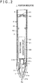
- FIG. 2 is a view explaining an exemplary configuration of the position indicator 1 as the first embodiment of the present invention. This view is primarily a partial longitudinal sectional view of the pen tip side. In this embodiment, the position indicator 1 is configured to have a pen-like appearance.
- the position indicator 1 of this embodiment has a pen-like housing 2.
- the housing 2 is configured, for example, using a hollow cylindrical insulator section 21 constituted by an insulating material such as a synthetic resin.
- a conductor section 22 made of a metal, for example.
- the conductor section 22 covering the outer periphery of the housing 2 is electrically connected with a ground conductor, not depicted, of the printed circuit board 3.
- the battery 4 may be a dry cell, a rechargeable storage cell, or a power supply circuit that includes a capacitor such as an electric double layer capacitor, to be discussed later.
- a signal transmission control circuit 30 and other electronic components and wiring patterns, not depicted, are arranged on the printed circuit board 3.
- the signal transmission control circuit 30 generates a position detection signal and additional information and outputs the generated position detection signal and additional information from the position indicator 1.
- the battery 4 is a power source that supplies power to the electronic circuits and electronic components configured on the printed circuit board 3.
- a terminal 42 is connected electrically with a power supply circuit section on the printed circuit board 3.
- a positive electrode 41 of the battery 4 is in contact with the terminal 42 for electrical connection therebetween.
- a negative electrode of the battery 4, not depicted, is either directly connected with the ground conductor of the printed circuit board 3 or pressed into contact with an elastically deformable terminal connected with the ground conductor of the printed circuit board 3 via the conductor section 22 of the housing 2.
- the writing pressure detection unit 5 is configured as a variable capacitance capacitor with its capacitance varying with the amount of writing pressure applied to a stylus 6.
- the electrodes at both ends of the variable capacitance capacitor constituted by the writing pressure detection unit 5 are connected to the signal transmission control circuit 30 via a conductive pattern 31c.
- the stylus 6 is latched inside a hollow space of the housing 2 of the position indicator 1 when the end of the stylus 6 opposite to the pen tip protruding out of the housing 2 is fitted into the writing pressure detection unit 5 installed in the hollow space of the housing 2.
- the stylus 6 is configured to be disengaged from the writing pressure detection unit 5 when pulled out. That is, the stylus is replaceable for the position indicator 1.
- the stylus 6 is constituted by a conductor such as a hard resin in which metal and conductor powder are mixed.
- the stylus 6 is electrically connected with the signal transmission control circuit 30 via a conductive pattern 31a.
- the stylus 6 is configured in such a manner that the position detection signal and additional information generated by the signal transmission control circuit 30 are output to the sensor of the position detection apparatus 201 via the stylus 6 (center electrode) constituted by the conductor.
- One end part the hollow cylindrical insulator section 21 in its center line direction constituting the housing 2 is a cylindrical tapered section 21a that is tapered toward its tip.
- a tapered cylindrical cone-shaped ring electrode 7 is attached to an inner wall surface of the cylindrical tapered section 21a in such a manner that the ring electrode 7 acting as a peripheral electrode encircles partially the stylus 6 as the center electrode in the axial center direction of the housing 2.
- the ring electrode 7 is arranged together with the housing 2 to encircle the stylus 6 in such a manner that a tip part of the stylus 6 is partially exposed.
- the ring electrode 7 forms a ring-like conductor constituted by a conductive member, for example.
- the ring electrode 7 is covered by the tapered section 21a of the insulator section 21 in the housing 2, so that the operator of the position indicator 1 does not directly touch the ring electrode 7.
- the ring electrode 7 as the peripheral electrode is not limited to a conical shape and may have a cylindrical shape or a ring-like shape.
- the ring electrode 7 is connected electrically with a conductor pattern 31b of the printed circuit board 3 via a lead conductor member 71 penetrating through the insulator section 21.
- the conductor pattern 31b is connected with the signal transmission control circuit 30.
- the signal transmission control circuit 30 is configured in such a manner that a signal opposite in phase to the signal from the stylus 6 is output from the ring electrode 7.
- the ring electrode 7 is connected to a part where a reference potential of the printed circuit board 3 appears via a coil 303, i.e., connected to the ground conductor in this example (see FIG. 3 ).
- the stylus 6 is arranged in a hollow space of the insulator section 21 in such a manner that a tip part 6a of the stylus 6 protrudes out of an opening 21b of the tapered section 21a of the insulator section 21 in the housing 2 and that the part opposite to the tip part 6a is fitted into the writing pressure detection unit 5. That is, the center electrode (stylus 6) and the peripheral electrode (ring electrode 7) are arranged in the axial center direction of the housing 2, with the center electrode encircled partially by the peripheral electrode in the axial center direction.
- the ring electrode 7 is attached to the inner wall surface of the tapered section 21a of the insulator section 21, so that the pen tip part 6a of the stylus 6 is projected externally without being encircled by the ring electrode 7.
- the ring electrode 7 encircling the stylus 6 is arranged with this embodiment in such a manner as to encircle the stylus circumference excluding a coupling portion between the pen tip part 6a and the writing pressure detection unit 5.
- the signal transmission control circuit 30 includes a circuit that generates the signal to be output to the sensor of the position detection apparatus 201 via the stylus 6, and a circuit that generates another signal opposite in phase to the signal to be output from the stylus 6.
- FIG. 3 is a circuit configuration diagram of the signal transmission control circuit 30 in the position indicator 1 of this embodiment.
- the signal transmission control circuit 30 includes a controller 301, an oscillation circuit 302 that generates the signal to be supplied to the stylus 6, and a coil 303 that outputs from the ring electrode 7 the signal that is opposite in phase to the signal output from the stylus 6. That is, the signals generated by the oscillation circuit 302 are supplied to the stylus 6 as well as to the ring electrode 7 via a stray capacitance 304 formed between the stylus 6 and the ring electrode 7.
- the embodiment includes the coil 303 that causes the signal output from the ring electrode 7 to be opposite in phase to the signal output from the stylus 6.
- the controller 301 configured with a microprocessor, for example, constitutes a control circuit that controls processing operations, to be discussed later, of the signal transmission control circuit 30 in the position indicator 1.
- the controller 301 is supplied with a power supply voltage VDD from the battery 4 acting as a typical drive power supply.
- the controller 301 controls the oscillation circuit 302.
- the power supply voltage VDD from the battery 4 is supplied via a power switch Psw to the signal transmission control circuit 30 and to other circuits.
- the power switch Psw not depicted in FIGS. 1 and 2 , has an operating element disposed on a side surface of the housing 2, the operating element being turned on and off when pressed.
- the controller 301 is also connected with a variable capacitance capacitor 5C configured using the writing pressure detection unit 5.
- the controller 301 monitors the capacitance of the variable capacitance capacitor 5C in order to detect the writing pressure applied to the stylus 6 of the position indicator 1.
- a discharging resistor Rd is connected with the variable capacitance capacitor 5C.
- the controller 301 detects the capacitance of the variable capacitance capacitor 5C by measuring a discharge time from the time the variable capacitance capacitor 5C is fully charged until it is discharged down to a predetermined end-to-end voltage. From the detected capacitance, the controller 301 detects the writing pressure.
- the oscillation circuit 302 is supplied with the power supply voltage VDD from the battery 4 via the power switch Psw.
- a continuous wave of the alternating-current signal i.e., a burst signal, from the oscillation circuit 302 over a predetermined time period constitutes a position detection signal to be output to the sensor via the stylus 6.
- the controller 301 causes the oscillation circuit 302 to generate the above-mentioned burst signal and an ASK (Amplitude Shift Keying) modulated signal by supplying a control signal (enable signal CT) to an enable terminal EN of the oscillation circuit 302 for on/off control of the oscillation circuit 302.
- the oscillation circuit 302 In response to the enable signal CT from the controller 301, the oscillation circuit 302 generates the alternating-current signal intermittently. This is how the oscillation circuit 302 generates the burst signal and the ASK-modulated signal.
- the controller 301 converts information regarding the writing pressure value detected as described above into a digital signal, and controls the oscillation circuit 302 in accordance with the digital signal. The controller 301 thus causes the oscillation circuit 302 to output the writing pressure value information as the ASK-modulated signal.
- the output terminal of the oscillation circuit 302 is connected with the conductive stylus 6 in this embodiment.
- the alternating-current signal from the oscillation circuit 302 is output to the sensor of the position detection apparatus 201 via the stylus 6.
- the ring electrode 7 is connected with the ground conductor (ground) via the coil 303.
- the ring electrode 7 encircling the stylus 6 is connected with the latter through the stray capacitance 304 therebetween. Consequently, an equivalent circuit of the signal transmission control circuit 30 is formed as depicted in FIG. 4 , enclosed by dotted lines.
- the signal generated by the oscillation circuit 302 is thus supplied to the stylus 6 as well as to the ring electrode 7 through capacitive coupling based on the stray capacitance 304.
- An alternating-current signal Sa from the stylus 6 is output from the ring electrode 7 as an alternating-current signal Sb inverted in phase by the coil 303.
- the signal transmission control circuit 30, which includes the oscillation circuit 302, causes a first signal and a second signal generated by the oscillation circuit 302 to be supplied to the stylus 6 (center electrode) and to the ring electrode 7 (peripheral electrode), respectively.
- the signal transmission control circuit 30 controls the signal output from the stylus 6 and the signal output from the ring electrode 7 in such a manner that the phases of these signals cancel each other (in an opposite phase relation). Further, the signal transmission control circuit 30 controls these signals to be in a predetermined amplitude level relation to each other such that the signals have their phases effectively cancelled out each other.
- the output signal from the oscillation circuit 302 of the position indicator 1 is output, with its intensity substantially intact, from the tip part 6a of the stylus 6 to the input surface 201S of the sensor of the position detection apparatus 201.
- the output signal from the oscillation circuit 302 is scarcely received by the sensor when output from that portion of the stylus 6 encircled by the ring electrode 7 and from that portion of the tip part 6a close to the ring electrode 7, because the signal is cancelled by the opposite-phase signal from the ring electrode 7.
- the position detection apparatus 201 can accurately detect the non-shifted position pointed by the tip part 6a of the stylus 6.
- the inductance value of the coil 303 is adjusted to a value such that even if the axial center direction of the stylus 6 of the position indicator 1 is tilted relative to the input surface 201S of the sensor of the position detection apparatus 201, the position detection apparatus 201 can correctly detect the position pointed by the tip part 6a of the stylus 6.
- stray capacitance 304 is virtually connected interposingly between the stylus 6 and the ring electrode 7 in the equivalent circuit of FIG. 4
- a capacitor may actually be connected interposingly between the stylus 6 and the ring electrode 7, with the capacitance of the capacitor adjusted to a value that allows the position detection apparatus accurately to detect the position pointed by the tip part 6a of the stylus 6.
- the capacitance of the capacitor actually connected interposingly between the stylus 6 and the ring electrode 7 may be adjusted instead of, or in conjunction with, adjusting the inductance value of the coil 303.
- the conductor section 22 is arranged to cover at least that portion of the outer periphery, held by the operator, of the insulator section 21 of the housing 2.
- the conductor section 22 is not mandatory and may be omitted.
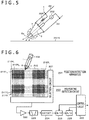
- the position detection apparatus 201 of this embodiment includes, as depicted in FIG. 6 , a sensor 202 constituting the position detection apparatus 201 and a pen pointing detection circuit 203 connected with the sensor 202.
- the senor 202 is configured with a first conductor group 211, an insulating layer (not depicted), and a second conductor group 212 stacked from the bottom up in that order.
- the first conductor group 211 has multiple first conductors 211Y 1 , 211Y 2 , ..., 211Y m (m is an integer of 1 or more) each extending in the crosswise direction (X-axis direction), for example, the first conductors being arranged in parallel a predetermined distance apart from each other in the Y-axis direction.
- the second conductor group 212 has multiple second conductors 212X 1 , 212X 2 , ..., 212X n (n is an integer of 1 or more) each extending in a direction intersecting with the extending direction of the first conductors 211Y 1 , 211Y 2 , ..., 211Y m , i.e., each extending in the perpendicular lengthwise direction (Y-axis direction) in this example, the second conductors being arranged in parallel a predetermined distance apart from each other in the X-axis direction.
- the sensor 202 of the position detection apparatus 201 is configured to detect the position pointed by the position indicator 1 through the use of a sensor pattern formed by the first conductor group 211 and the second conductor group 212 intersecting with each other.
- the first conductors 211Y 1 , 211Y 2 , ..., 211Y m will be collectively referred to as the first conductors 211Y where there is no need to distinguish the individual conductors.
- the second conductors 212X 1 , 212X 2 , ..., 212X n will be collectively referred to as the second conductors 212X where there is no need to distinguish the individual conductors.
- the sensor 202 of the position detection apparatus 201 of this embodiment includes a sensor surface (pointing input surface) 200 whose size is comparable to that of the display screen of an electronic device such as a tablet type information terminal.
- the sensor 202 is configured with the first conductor group 211 and second conductor group 212 that are optically transparent.
- first conductor group 211 and the second conductor group 212 may be both arranged on the same side of the sensor substrate.
- first conductor group 211 may be arranged on one side of the sensor substrate and the second conductor group 212 on the other side thereof.
- the pen pointing detection circuit 203 includes a selection circuit 221 acting as an input/output interface with the sensor 202, an amplification circuit 222, a band-pass filter 223, a detection circuit 224, a sample hold circuit 225, an AD (Analog to Digital) conversion circuit 226, and a control circuit 220.
- the selection circuit 221 selects one conductor from the first conductor group 211 and one conductor from the second conductor group 212.
- the conductors selected by the selection circuit 221 are connected to the amplification circuit 222.
- the signal from the position indicator 1 is detected by the selected conductors and amplified by the amplification circuit 222.
- the output of the amplification circuit 222 is supplied to the band-pass filter 223 that extracts only the frequency component of the signal transmitted from the position indicator 1.
- the output signal of the band-pass filter 223 is detected by the detection circuit 224.
- the output signal of the detection circuit 224 is supplied to the sample hold circuit 225.
- a sampling signal from the control circuit 220 causes the sample hold circuit 225 to sample and hold the supplied signal at a predetermined timing.
- the result of the sample hold operation is converted to a digital value by the AD conversion circuit 226.
- the digital data from the AD conversion circuit 226 is read and processed by the control circuit 220.
- control circuit 220 acts to output control signals to the sample hold circuit 225, to the AD conversion circuit 226, and to the selection circuit 221. Given the digital data from the AD conversion circuit 226, the control circuit 220 calculates the coordinates of the position on the sensor 202 pointed by the position indicator 1 and obtains writing pressure information through demodulation. The control circuit 220 then outputs the position coordinate data and the writing pressure information to another processor in an electronic device such as a tablet type information terminal.
- FIG. 7 depicts how the tilt angle of the axial center direction of the stylus 6 of the position indicator 1 with respect to the input surface 201S of the sensor 202 is related to the signal levels of the signal received from the position indicator 1 by the sensor 202 of the position detection apparatus 201.
- the signal levels of the signal received by multiple second conductors 212X arranged in the X-axis direction (e.g., crosswise direction) of the sensor 202 in the example of FIG. 7 , conductors Xi-2, Xi-1, Xi, Xi+1, and Xi+2).
- FIG. 7(A) illustrates the signal levels of the signal received by the first conductors Xi-2, Xi-1, Xi, Xi+1, and Xi+2 in a case where the axial center direction of the stylus 6 of the position indicator 1 is perpendicular to the input surface 201S of the sensor 202 of the position detection apparatus 201 and where the tip part 6a of the stylus 6 is directly above the first conductor Xi, with the conductors Xi-2, Xi-1, Xi+1 and Xi+2 positioned nearby.
- the signal from the stylus 6 is transmitted substantially from the tip part 6a of the stylus 6 to the sensor 202, with the ring electrode 7 outputting the opposite-phase signal to the sensor 202. Consequently, as in the case of FIG. 11(A) , the signal level of the signal received by each of the second conductors Xi-2, Xi-1, Xi, Xi+1 and Xi+2 is highest on the second conductor Xi at the center and is progressively lower on the second conductors Xi-2 and Xi-1 to the left of the second conductor Xi and on the second conductors Xi+1 and Xi+2 to the right thereof in a symmetrical manner.
- the second conductors Xi-2 and Xi-1 to the left side of the second conductor Xi and the second conductors Xi+1 and Xi+2 to the right side thereof have their signal levels decreasing more steeply than in the case of FIG. 11(A) .
- the position detection apparatus calculates the position on the sensor pointed by the tip part 6a of the stylus 6, using the received signal levels of the second conductors Xi-2, Xi-1, Xi, Xi+1 and Xi+2.
- the position pointed by the tip part 6a of the stylus 6 is detected more suitably as the position P0 of the second conductor Xi. That is because the received signal level of the second conductor Xi is appreciably higher than those of the second conductors Xi-2 and Xi-1 to the left and those of the second conductor Xi+1 and Xi+2 to the right by an amount larger than in the case of FIG. 11(A) .
- FIG. 7(B) depicts the signal levels of the signal received by the second conductors Xi-2, Xi-1, Xi, Xi+1, and Xi+2 in a case where the tip part 6a of the stylus 6 of the position indicator 1 is directly above the second conductor Xi but where the stylus 6 is tilted in the X-axis direction at an angle ⁇ ( ⁇ ⁇ 90 degrees) with respect to the input surface 201S of the sensor 202 of the position detection apparatus 201.
- the ring electrode 7 approaches the input surface 201S of the sensor of the position detection apparatus 201.
- the signal from the stylus 6 is then transmitted to the sensor not only from the tip part 6a of the stylus 6 but also from other parts of the stylus 6 that are near the sensor in keeping with the tilt of the position indicator 1, as depicted in FIG. 11(B) .
- the signal component from the nearby parts of the stylus 6 is cancelled out by the opposite-phase signal from the ring electrode 7.
- the signal level of the signal received by each of the second conductors Xi-2, Xi-1, Xi, Xi+1 and Xi+2 is highest on the second conductor Xi at the center and represents on the second conductors Xi-2 and Xi-1 to the left of the second conductor Xi and on the second conductors Xi+1 and Xi+2 to the right thereof in a symmetrical manner, as illustrated by solid lines in FIG. 7(B) .
- the position detection apparatus detects the position on the sensor pointed by the tip part 6a of the stylus 6 as the position P0 of the second conductor Xi with a minimum of shift through calculations using the received signal levels of the second conductors Xi-2, Xi-1, Xi, Xi+1 and Xi+2, as in the case of FIG. 7(A) .
- the ring electrode 7 is connected to the ground conductor via the coil 303.
- the ring electrode 7 may be connected to a terminal on which the power supply voltage VDD is made to appear. That is, it is sufficient to connect the ring electrode 7 to the reference potential via the coil 303.
- the signal transmission control circuit 30 is configured to connect the ring electrode 7 to the reference potential through the coil 303 in order to output the signal that is opposite in phase to the signal output from the stylus 6.
- this configuration is not limitative of how the opposite-phase signal is to be output.
- FIG. 8 depicts a first alternative example configured to cause the ring electrode 7 to output the signal opposite in phase to the signal output from the stylus 6.
- the signal transmission control circuit 30A in this first example does not include the coil 303 to be connected with the ring electrode 7.
- the first embodiment is modified to include a polarity inversion amplifier 305 that supplies the stylus 6 with the signal from the oscillation circuit 302 while acting as an opposite-phase signal generation circuit for generating the signal opposite in phase to the signal from the oscillation circuit 302.
- the polarity inversion amplifier 305 inverts the signal from the oscillation circuit 302 and supplies the inverted signal to the ring electrode 7.
- the amplification gain of the polarity inversion amplifier 305 is adjusted to a value such that the position detection apparatus 201 can correctly detect the position pointed by the tip part 6a of the stylus 6.
- the signal opposite in phase to the signal from the stylus 6 is output from the ring electrode 7. This provides advantageous effects similar to those of the foregoing first embodiment.
- FIG. 9 depicts a second alternative example configured to constitute an opposite-phase signal generation circuit using a transformer 306.
- the ring electrode 7 outputs the signal opposite in phase to the signal from the stylus 6, without using the coil 303.
- a signal transmission control circuit 30B of this second example as depicted in FIG. 9(A) , the signal from the oscillation circuit 302 of the first embodiment is supplied to the stylus 6 via the transformer 306 that has a primary winding 306a and a secondary winding 306b. Also, the signal from the oscillation circuit 302 is supplied from the side of the primary winding 306a of the transformer 306.
- FIG. 9(B) depicts a modification of the second example.
- the primary winding 306a is provided with an intermediate tap, as depicted in in FIG. 9(B) .
- the signal from the oscillation circuit 302 is arranged to be supplied from the intermediate tap of the primary winding 306a to the ring electrode 7.
- the position of the intermediate tap on the primary winding 306a may be adjusted in such a manner that the position detection apparatus 201 can correctly detect the position pointed by the tip part 6a of the stylus 6.
- the signal from the oscillation circuit 302 is supplied to the stylus 6 from the secondary winding 306b of the transformer 306 and to the ring electrode 7 from the primary winding 306a of the transformer 306.
- the signal output from the stylus 6 and the signal from the ring electrode 7 are thus opposite to each other in phase. This provides advantageous effects similar to those of the foregoing first embodiment.
- the ring electrode 7 is arranged to output the signal opposite in phase to the signal from the stylus 6. This raises a possibility that the signal from the ring electrode 7 may lower the output intensity of the signal from the stylus 6.
- the position detection apparatus 201 need not precisely detect the position pointed by the tip part 6a of the stylus 6 of the position indicator 1. In this state, the position detection apparatus 201 need only detect an appropriate position on the input surface of the sensor that the stylus 6 of the position indicator 1 has approached. Thus, the higher the output intensity of the signal from the position indicator, the better the result.
- the ring electrode 7 may be arranged to output the signal opposite in phase to the signal from the stylus 6 only when the tip part 6a of the stylus 6 of the position indicator 1 is in contact with the input surface of the sensor for accurate detection of the position pointed by the tip part 6a of the stylus 6.
- the ring electrode 7 may be arranged not to output the opposite-phase signal so as not to lower the output intensity of the signal output from the position indicator.
- the amplitude level of the signal output from the stylus 6 and that of the signal from the ring electrode 7 may be adjusted in a manner maintaining an optimum amplitude level relation therebetween, as in the case of FIG. 8 .
- FIG. 10 depicts an exemplary circuit configuration of a signal transmission control circuit 30D in the position indicator 1 that takes into account what is discussed above.
- the signal transmission control circuit 30D in FIG. 10 is a modification of the above-described signal transmission control circuit 30 depicted in FIG. 3 .
- the same components as those in the signal transmission control circuit 30 are designated by the same reference numerals and their explanations are omitted.
- a switch circuit 307 as a typical control circuit is connected to the ring electrode 7.
- the signal from the oscillation circuit 302 is supplied not only to the stylus 6 but also to one fixed terminal of the switch circuit 307.
- Another fixed terminal of the switch circuit 307 is grounded via the coil 303.
- a movable terminal of the switch circuit 307 is connected to the ring electrode.
- a controller 301D of this example detects the writing pressure applied to the stylus 6 of the position indictor 1 by monitoring the capacitance of the variable capacitance capacitor 5C constituted by the writing pressure detection unit 5. Given the result of detection of the writing pressure, the controller 301D determines whether or not the tip part 6a of the stylus 6 is in contact with the input surface of the sensor of the position detection apparatus 201. On the basis of the result of the determination, the controller 301D generates a switching control signal SW1 for the switch circuit 307, and controls the switching operation of the switch circuit 307 as follows.
- the controller 301D when determining that there is no writing pressure applied to the stylus 6 and that the tip part 6a of the stylus 6 is therefore not in contact with the input surface of the sensor of the position detection apparatus 201, the controller 301D generates the switching control signal SW1 such as to set the switch circuit 307 to the fixed terminal to which the signal from the oscillation circuit 302 is supplied. At this point, the coil 303 is disconnected from the ring electrode 7 so that the ring electrode 7 does not output the signal opposite in phase to the signal from the stylus 6. The ring electrode 7 thus outputs the signal in phase with the signal from the stylus 6. This enables the position detection apparatus 201, given the signals from the stylus 6 and from the ring electrode 7, to detect an approaching tip part 6a of the stylus 6 of the position indicator 1 with higher sensitivity than if only the signal from the stylus 6 is monitored.
- the controller 301D Upon determining that the writing pressure applied to the stylus 6 is detected and that the tip part 6a of the stylus 6 is therefore in contact with the input surface of the sensor of the position detection apparatus 201, the controller 301D generates the switching control signal SW1 such as to set the switch circuit 207 to the fixed terminal with which the coil 303 is connected. At this point, as in the case of the first embodiment, the coil 303 is connected to the ring electrode 7. In this state, the ring electrode 7 outputs the signal opposite in phase to the signal from the stylus 6. This makes it possible suitably to detect the position of the tip part 6a of the stylus 6 of the position indicator 1 even if the position indicator 1 is tilted relative to the input surface of the sensor.
- the control circuit in the example of FIG. 10 has the switch circuit 307 configured for switching control using the switching control signal SW1.
- a first switch circuit may be interposed between the ring electrode 6 and the coil 303 and a second switch circuit between the oscillation circuit 302 and the ring electrode 7.
- the example in FIG. 10 is an exemplary configuration in which the ring electrode 7 does not output the opposite-phase signal when the tip part 6a of the stylus 6 is determined to be not in contact with the input surface of the sensor of the position detection apparatus 201.
- the technical concept of the example in FIG. 10 can also be applied to the example in FIG. 8 in which the ring electrode 7 outputs the opposite-phase signal, as well as to the example depicted in FIG. 9 .
- the ring electrode 7 constituting the ring-like conductor has a conical shape that is tapered toward the tip part 6a of the stylus 6.
- the conical shape is not limitative of the appearance of the ring-like conductor. The point is that the ring-like conductor need only have a shape that encircles the circumference of the stylus 6, such as a cylindrical shape or a donut-like shape.
- the stylus 6 center electrode
- the ring electrode 7 peripheral electrode
- the stylus 6 and the ring electrode 7 need only have a phase relation configured to output the signals of which the phases are cancelled out, i.e., signals that are opposite to each other in phase.
- the signal supplied to the stylus 6 and the signal supplied to the ring electrode 7 may be replaced with each other.
- the information regarding the writing pressure applied to the stylus of the position indicator is output from the stylus 6 together with the position detection signal.
- wireless communication means complying with the Bluetooth (registered trademark) standard may be provided to the position indicator and to the position detection apparatus for wireless communication therebetween.
Landscapes
- Engineering & Computer Science (AREA)
- General Engineering & Computer Science (AREA)
- Theoretical Computer Science (AREA)
- Human Computer Interaction (AREA)
- Physics & Mathematics (AREA)
- General Physics & Mathematics (AREA)
- Position Input By Displaying (AREA)
Abstract
Description
- The present invention relates to a position indicator that operates by a capacitance method to interact capacitively with a sensor of a position detection apparatus.
- There exist known active capacitive pens each acting as a position indicator of the above-mentioned type operating by the capacitance method, the position indicator having a signal transmission circuit that transmits a signal via a conductive stylus to a sensor of a position detection apparatus through capacitive coupling. In this case, the position detection apparatus receives a signal from the active capacitive pen via the sensor that includes multiple sensor conductors. The position detection apparatus detects the position on the sensor that is pointed by a pen tip of a stylus of the active capacitive pen in accordance with a signal level on the sensor conductors having received the signal.
- When the axial center direction of the stylus is perpendicular to an input surface of the sensor, the position detection apparatus can detect the position pointed by the pen tip of the stylus with substantial accuracy. One problem is that when the axial center direction of the stylus is tilted relative to the input surface of the sensor, the position detection apparatus cannot accurately detect the position pointed by the pen tip of the stylus.
-
FIG. 11 is a view explaining a relationship between the tilt angles of the axial center direction of the stylus of the position indicator relative to the input surface of the sensor on one hand and the signal levels of the signal received by the sensor of the position detection apparatus from the position indicator on the other hand.FIG. 11 illustrates the signal levels of the signal received by multiple conductors (conductors Xi-2, Xi-1, Xi, Xi+1, and Xi+2 in the example ofFIG. 11 ) arranged in an X-axis direction (e.g., crosswise direction) of the sensor. The sensor has multiple conductors arranged likewise in a Y-axis direction as well. Similar signal levels also appear on these conductors arranged in the Y-axis direction. -
FIG. 11(A) indicates the signal levels of the signal received by the conductors Xi-2, Xi-1, Xi, Xi+1, and Xi+2 in a case where the axial center direction of astylus 100 of the position indicator is perpendicular to the input surface of the sensor of the position detection apparatus and where the stylus 100 (i.e., its pen tip) is directly above the conductor Xi. In this case, the signal from thestylus 100 is transmitted substantially from the tip of the stylus to the sensor. As a result, the signal level of the signal received by each of the conductors Xi-2, Xi-1, Xi, Xi+1 and Xi+2 is highest on the conductor Xi at the center and is progressively lower on the conductors Xi-2 and Xi-1 to the left of the conductor Xi and on the conductors Xi+1 and Xi+2 to the right thereof in a symmetrical manner, as illustrated inFIG. 11(A) . - The position detection apparatus detects the position on the sensor pointed by the
stylus 100 by performing calculations using the signal levels of the signal received by the conductors Xi-2, Xi-1, Xi, Xi+1, and Xi+2. In the case ofFIG. 11(A) , a position P0 (X coordinate) pointed by thestylus 100 is detected correctly as the position of the conductor Xi. - On the other hand,
FIG. 11(B) depicts the signal levels of the signal received by the conductors Xi-2, Xi-1, Xi, Xi+1, and Xi+2 in a case where the pen tip of thestylus 100 of the position indicator is directly above the conductor Xi but where thestylus 100 is tilted relative to the input surface of the sensor of the position detection apparatus at a predetermined angle θ (θ < 90 degrees) in the X-axis direction. In this case, the signal from thestylus 100 is transmitted to the sensor not only from the stylus tip but also effectively from a stylus portion close to the sensor in keeping with the tilt. As a result, the signal level of the signal received by each of the conductors Xi-2, Xi-1, Xi, Xi+1 and Xi+2 is highest on the conductor Xi at the center and is progressively lower on the conductors Xi-2 and Xi-1 to the left of the conductor Xi and on the conductors Xi+1 and Xi+2 to the right thereof in an asymmetrical manner in keeping with the tilt of thestylus 100, as depicted inFIG. 11(B) . - The position detection apparatus detects the position pointed by the
stylus 100 by performing calculations using the signal levels of the signal received by the conductors Xi-2, Xi-1, Xi, Xi+1, and Xi+2 in the state inFIG. 11(B) . Consequently, the position pointed by thestylus 100 is shifted to a position P1 in the direction in which thestylus 100 is tilted by the amount reflecting the tilt angle. The position P1 deviates by ΔP from the position P0 pointed by the tip of thestylus 100. - Methods have been proposed to solve the problem of the shift in the position pointed by the pen tip of the stylus of the position indicator reflecting the tilt of the latter. The proposed methods, such as the detection method disclosed in
Patent Document 1 and the detection method disclosed inPatent Document 2, propose detecting the tilt angle of the position indicator relative to the input surface of the sensor (i.e., tilt angle of the stylus in the axial center direction) and, by use of the result of the detection, correcting the detected position pointed by the pen tip of the stylus of the position indicator. -
- Patent Document 1: Japanese Patent Laid-open No.
2014-35631 - Patent Document 2: Japanese Patent Laid-open No.
2016-126503 - However, a configuration for detecting the tilt angle is needed with the proposed methods that involve detecting the tilt angle of the position indicator with respect to the input surface of the sensor and, by use of the result of the detection, correcting the detected position pointed by the pen tip of the stylus of the position indicator. This poses the problem of complicating the configuration of the position indicator and raising its manufacturing cost as well.
- It is an object of the present invention to provide a position indicator that solves the above problem.
- In order to solve the above problems, the present invention provides a position indicator including a pen-like housing, a first electrode, a second electrode, and a signal transmission control circuit, the first electrode and the second electrode being arranged at one end of the housing in an axial center direction thereof, the second electrode being arranged to encircle the first electrode in such a manner as to let the first electrode be partially exposed in the axial center direction of the housing, the signal transmission control circuit supplying the first electrode and the second electrode with a signal such as to interact electrostatically with a sensor of a position detection apparatus. The signal transmission control circuit is configured to supply the first electrode and the second electrode with the signals such that the signal output from the first electrode and the signal output from the second electrode are cancelled out each other.
- According to the position indicator of the above configuration, even if the axial center direction of the stylus is tilted relative to the input surface of the sensor of the position detection apparatus, the coordinates of the position pointed by the pen tip of the stylus are prevented from being shifted on the part of the position detection apparatus.
-
- [
FIG. 1 ]
FIG. 1 is a view depicting an example of a tablet type information terminal as a typical electronic device that uses a position indicator as a first embodiment of the present invention. - [
FIG. 2 ]
FIG. 2 is a view explaining an exemplary configuration of the position indicator as the first embodiment of the present invention. - [
FIG. 3 ]
FIG. 3 is a block diagram depicting an exemplary configuration of a signal transmission control circuit of the position indicator as the first embodiment of the present invention. - [
FIG. 4 ]
FIG. 4 is a view depicting an equivalent circuit of the signal transmission control circuit inFIG. 3 . - [
FIG. 5 ]
FIG. 5 is a view explaining the relationship between the signal output from the position indicator as the first embodiment of the present invention on one hand and a position detection apparatus on the other hand. - [
FIG. 6 ]
FIG. 6 is a view explaining an exemplary configuration of the position detection apparatus for use with the position indicator according to the present invention. - [
FIG. 7 ]
FIG. 7 is a view explaining how the signal is received by the position detection apparatus in a case where the position indicator as the first embodiment of the present invention is used. - [
FIG. 8 ]
FIG. 8 depicts a view explaining a modification of the main section of the position indicator according to the present invention. - [
FIG. 9 ]
FIG. 9 depicts views explaining other modifications of the main section of the position indicator according to the present invention. - [
FIG. 10 ]
FIG. 10 is a view explaining the main section of another embodiment of the position indicator according to the present invention. - [
FIG. 11 ]
FIG. 11 is a view explaining how the signal is received by the position detection apparatus in a case where an existing position indicator is used. - Some embodiments of the position indicator according to the present invention are described below with reference to the accompanying drawings.
-
FIG. 1 depicts an example of a tablettype information terminal 200 as a typical electronic device that uses aposition indicator 1 as an embodiment of the present invention. In this example, the tablettype information terminal 200 includes adisplay screen 200D of a display apparatus such as an LCD (Liquid Crystal Display). The upper side of thedisplay screen 200D (surface side) includes a sensor of aposition detection apparatus 201 operating by the capacitance method. - Using the
position indicator 1, an operator points a position on aninput surface 201S of the sensor of theposition detection apparatus 201 in the tablettype information terminal 200. Theposition detection apparatus 201 detects the position pointed by theposition indicator 1 on the sensor of theposition detection apparatus 201. -
FIG. 2 is a view explaining an exemplary configuration of theposition indicator 1 as the first embodiment of the present invention. This view is primarily a partial longitudinal sectional view of the pen tip side. In this embodiment, theposition indicator 1 is configured to have a pen-like appearance. - The
position indicator 1 of this embodiment has a pen-like housing 2. Thehousing 2 is configured, for example, using a hollowcylindrical insulator section 21 constituted by an insulating material such as a synthetic resin. With this embodiment, at least that portion of an outer periphery of theinsulator section 21 that is held by the operator along thehousing 2 is covered with aconductor section 22 made of a metal, for example. - Inside the
housing 2 are a printedcircuit board 3, abattery 4 serving as a power supply circuit, and a writingpressure detection unit 5. Theconductor section 22 covering the outer periphery of thehousing 2 is electrically connected with a ground conductor, not depicted, of the printedcircuit board 3. Thebattery 4 may be a dry cell, a rechargeable storage cell, or a power supply circuit that includes a capacitor such as an electric double layer capacitor, to be discussed later. - A signal
transmission control circuit 30 and other electronic components and wiring patterns, not depicted, are arranged on the printedcircuit board 3. The signaltransmission control circuit 30 generates a position detection signal and additional information and outputs the generated position detection signal and additional information from theposition indicator 1. - The
battery 4 is a power source that supplies power to the electronic circuits and electronic components configured on the printedcircuit board 3. A terminal 42 is connected electrically with a power supply circuit section on the printedcircuit board 3. Apositive electrode 41 of thebattery 4 is in contact with the terminal 42 for electrical connection therebetween. A negative electrode of thebattery 4, not depicted, is either directly connected with the ground conductor of the printedcircuit board 3 or pressed into contact with an elastically deformable terminal connected with the ground conductor of the printedcircuit board 3 via theconductor section 22 of thehousing 2. - In this embodiment, the writing
pressure detection unit 5 is configured as a variable capacitance capacitor with its capacitance varying with the amount of writing pressure applied to astylus 6. InFIG. 2 , the electrodes at both ends of the variable capacitance capacitor constituted by the writingpressure detection unit 5 are connected to the signaltransmission control circuit 30 via aconductive pattern 31c. - The
stylus 6 is latched inside a hollow space of thehousing 2 of theposition indicator 1 when the end of thestylus 6 opposite to the pen tip protruding out of thehousing 2 is fitted into the writingpressure detection unit 5 installed in the hollow space of thehousing 2. Thestylus 6 is configured to be disengaged from the writingpressure detection unit 5 when pulled out. That is, the stylus is replaceable for theposition indicator 1. - The
stylus 6 is constituted by a conductor such as a hard resin in which metal and conductor powder are mixed. Thestylus 6 is electrically connected with the signaltransmission control circuit 30 via aconductive pattern 31a. Thestylus 6 is configured in such a manner that the position detection signal and additional information generated by the signaltransmission control circuit 30 are output to the sensor of theposition detection apparatus 201 via the stylus 6 (center electrode) constituted by the conductor. - One end part the hollow
cylindrical insulator section 21 in its center line direction constituting thehousing 2 is a cylindricaltapered section 21a that is tapered toward its tip. A tapered cylindrical cone-shapedring electrode 7 is attached to an inner wall surface of the cylindricaltapered section 21a in such a manner that thering electrode 7 acting as a peripheral electrode encircles partially thestylus 6 as the center electrode in the axial center direction of thehousing 2. In other words, thering electrode 7 is arranged together with thehousing 2 to encircle thestylus 6 in such a manner that a tip part of thestylus 6 is partially exposed. Thering electrode 7 forms a ring-like conductor constituted by a conductive member, for example. In this case, thering electrode 7 is covered by the taperedsection 21a of theinsulator section 21 in thehousing 2, so that the operator of theposition indicator 1 does not directly touch thering electrode 7. Incidentally, thering electrode 7 as the peripheral electrode is not limited to a conical shape and may have a cylindrical shape or a ring-like shape. - Also, the
ring electrode 7 is connected electrically with aconductor pattern 31b of the printedcircuit board 3 via alead conductor member 71 penetrating through theinsulator section 21. In this example, theconductor pattern 31b is connected with the signaltransmission control circuit 30. The signaltransmission control circuit 30 is configured in such a manner that a signal opposite in phase to the signal from thestylus 6 is output from thering electrode 7. With this embodiment, as will be discussed later, thering electrode 7 is connected to a part where a reference potential of the printedcircuit board 3 appears via acoil 303, i.e., connected to the ground conductor in this example (seeFIG. 3 ). - In this embodiment, the
stylus 6 is arranged in a hollow space of theinsulator section 21 in such a manner that atip part 6a of thestylus 6 protrudes out of anopening 21b of the taperedsection 21a of theinsulator section 21 in thehousing 2 and that the part opposite to thetip part 6a is fitted into the writingpressure detection unit 5. That is, the center electrode (stylus 6) and the peripheral electrode (ring electrode 7) are arranged in the axial center direction of thehousing 2, with the center electrode encircled partially by the peripheral electrode in the axial center direction. - In the example of
FIG. 2 , thering electrode 7 is attached to the inner wall surface of the taperedsection 21a of theinsulator section 21, so that thepen tip part 6a of thestylus 6 is projected externally without being encircled by thering electrode 7. - That is, the
ring electrode 7 encircling thestylus 6 is arranged with this embodiment in such a manner as to encircle the stylus circumference excluding a coupling portion between thepen tip part 6a and the writingpressure detection unit 5. - The signal
transmission control circuit 30 includes a circuit that generates the signal to be output to the sensor of theposition detection apparatus 201 via thestylus 6, and a circuit that generates another signal opposite in phase to the signal to be output from thestylus 6. -
FIG. 3 is a circuit configuration diagram of the signaltransmission control circuit 30 in theposition indicator 1 of this embodiment. In this example, the signaltransmission control circuit 30 includes acontroller 301, anoscillation circuit 302 that generates the signal to be supplied to thestylus 6, and acoil 303 that outputs from thering electrode 7 the signal that is opposite in phase to the signal output from thestylus 6. That is, the signals generated by theoscillation circuit 302 are supplied to thestylus 6 as well as to thering electrode 7 via astray capacitance 304 formed between thestylus 6 and thering electrode 7. Thus, the embodiment includes thecoil 303 that causes the signal output from thering electrode 7 to be opposite in phase to the signal output from thestylus 6. - The
controller 301, configured with a microprocessor, for example, constitutes a control circuit that controls processing operations, to be discussed later, of the signaltransmission control circuit 30 in theposition indicator 1. Thecontroller 301 is supplied with a power supply voltage VDD from thebattery 4 acting as a typical drive power supply. Thecontroller 301 controls theoscillation circuit 302. The power supply voltage VDD from thebattery 4 is supplied via a power switch Psw to the signaltransmission control circuit 30 and to other circuits. The power switch Psw, not depicted inFIGS. 1 and2 , has an operating element disposed on a side surface of thehousing 2, the operating element being turned on and off when pressed. - The
controller 301 is also connected with avariable capacitance capacitor 5C configured using the writingpressure detection unit 5. Thecontroller 301 monitors the capacitance of thevariable capacitance capacitor 5C in order to detect the writing pressure applied to thestylus 6 of theposition indicator 1. In this embodiment, that is, a discharging resistor Rd is connected with thevariable capacitance capacitor 5C. Thecontroller 301 detects the capacitance of thevariable capacitance capacitor 5C by measuring a discharge time from the time thevariable capacitance capacitor 5C is fully charged until it is discharged down to a predetermined end-to-end voltage. From the detected capacitance, thecontroller 301 detects the writing pressure. - The
oscillation circuit 302 generates an alternating-current signal with a frequency f1 = 1.8 MHz, for example. Theoscillation circuit 302 is supplied with the power supply voltage VDD from thebattery 4 via the power switch Psw. A continuous wave of the alternating-current signal i.e., a burst signal, from theoscillation circuit 302 over a predetermined time period constitutes a position detection signal to be output to the sensor via thestylus 6. - The
controller 301 causes theoscillation circuit 302 to generate the above-mentioned burst signal and an ASK (Amplitude Shift Keying) modulated signal by supplying a control signal (enable signal CT) to an enable terminal EN of theoscillation circuit 302 for on/off control of theoscillation circuit 302. In response to the enable signal CT from thecontroller 301, theoscillation circuit 302 generates the alternating-current signal intermittently. This is how theoscillation circuit 302 generates the burst signal and the ASK-modulated signal. In this embodiment, thecontroller 301 converts information regarding the writing pressure value detected as described above into a digital signal, and controls theoscillation circuit 302 in accordance with the digital signal. Thecontroller 301 thus causes theoscillation circuit 302 to output the writing pressure value information as the ASK-modulated signal. - The output terminal of the
oscillation circuit 302 is connected with theconductive stylus 6 in this embodiment. The alternating-current signal from theoscillation circuit 302 is output to the sensor of theposition detection apparatus 201 via thestylus 6. - The
ring electrode 7 is connected with the ground conductor (ground) via thecoil 303. In this case, thering electrode 7 encircling thestylus 6 is connected with the latter through thestray capacitance 304 therebetween. Consequently, an equivalent circuit of the signaltransmission control circuit 30 is formed as depicted inFIG. 4 , enclosed by dotted lines. The signal generated by theoscillation circuit 302 is thus supplied to thestylus 6 as well as to thering electrode 7 through capacitive coupling based on thestray capacitance 304. An alternating-current signal Sa from thestylus 6 is output from thering electrode 7 as an alternating-current signal Sb inverted in phase by thecoil 303. - That is, the signal
transmission control circuit 30, which includes theoscillation circuit 302, causes a first signal and a second signal generated by theoscillation circuit 302 to be supplied to the stylus 6 (center electrode) and to the ring electrode 7 (peripheral electrode), respectively. The signaltransmission control circuit 30 controls the signal output from thestylus 6 and the signal output from thering electrode 7 in such a manner that the phases of these signals cancel each other (in an opposite phase relation). Further, the signaltransmission control circuit 30 controls these signals to be in a predetermined amplitude level relation to each other such that the signals have their phases effectively cancelled out each other. - Consequently, as depicted in
FIG. 5 ., the output signal from theoscillation circuit 302 of theposition indicator 1 is output, with its intensity substantially intact, from thetip part 6a of thestylus 6 to theinput surface 201S of the sensor of theposition detection apparatus 201. However, the output signal from theoscillation circuit 302 is scarcely received by the sensor when output from that portion of thestylus 6 encircled by thering electrode 7 and from that portion of thetip part 6a close to thering electrode 7, because the signal is cancelled by the opposite-phase signal from thering electrode 7. As a result, as depicted inFIG. 5 , even if the axial center direction of thestylus 6 of theposition indicator 1 is tilted relative to theinput surface 201S of the sensor of theposition detection apparatus 201, theposition detection apparatus 201 can accurately detect the non-shifted position pointed by thetip part 6a of thestylus 6. - In this case, the inductance value of the
coil 303 is adjusted to a value such that even if the axial center direction of thestylus 6 of theposition indicator 1 is tilted relative to theinput surface 201S of the sensor of theposition detection apparatus 201, theposition detection apparatus 201 can correctly detect the position pointed by thetip part 6a of thestylus 6. - In other words, by adjusting the inductance value of the
coil 303, it is possible to adjust the intensity of the signal which is output from thering electrode 7 and of which the phase is opposite to that of the signal output from thestylus 6. This eliminates the need for extending thering electrode 7 up to near thetip part 6a of thestylus 6, allowing thering electrode 7 to be positioned as desired. This in turn reduces constraints on the external design of the position indicator. Obviously, it is possible to adjust how much thetip part 6a of thestylus 6 is allowed to protrude from thering electrode 7 so as to regulate the intensity of the signal which is output from thering electrode 7 and which is opposite in phase to the signal from thestylus 6. - Whereas the
stray capacitance 304 is virtually connected interposingly between thestylus 6 and thering electrode 7 in the equivalent circuit ofFIG. 4 , a capacitor may actually be connected interposingly between thestylus 6 and thering electrode 7, with the capacitance of the capacitor adjusted to a value that allows the position detection apparatus accurately to detect the position pointed by thetip part 6a of thestylus 6. In this case, the capacitance of the capacitor actually connected interposingly between thestylus 6 and thering electrode 7 may be adjusted instead of, or in conjunction with, adjusting the inductance value of thecoil 303. - With the above-described
position indicator 1, theconductor section 22 is arranged to cover at least that portion of the outer periphery, held by the operator, of theinsulator section 21 of thehousing 2. However, theconductor section 22 is not mandatory and may be omitted. - The
position detection apparatus 201 of this embodiment includes, as depicted inFIG. 6 , asensor 202 constituting theposition detection apparatus 201 and a pen pointingdetection circuit 203 connected with thesensor 202. - In this example, with no sectional view provided, the
sensor 202 is configured with a first conductor group 211, an insulating layer (not depicted), and a second conductor group 212 stacked from the bottom up in that order. The first conductor group 211 has multiple first conductors 211Y1, 211Y2, ..., 211Ym (m is an integer of 1 or more) each extending in the crosswise direction (X-axis direction), for example, the first conductors being arranged in parallel a predetermined distance apart from each other in the Y-axis direction. - The second conductor group 212 has multiple
second conductors - As described above, the
sensor 202 of theposition detection apparatus 201 is configured to detect the position pointed by theposition indicator 1 through the use of a sensor pattern formed by the first conductor group 211 and the second conductor group 212 intersecting with each other. - In the description that follows, the first conductors 211Y1, 211Y2, ..., 211Ym will be collectively referred to as the first conductors 211Y where there is no need to distinguish the individual conductors. Likewise, the
second conductors second conductors 212X where there is no need to distinguish the individual conductors. - The
sensor 202 of theposition detection apparatus 201 of this embodiment includes a sensor surface (pointing input surface) 200 whose size is comparable to that of the display screen of an electronic device such as a tablet type information terminal. Thesensor 202 is configured with the first conductor group 211 and second conductor group 212 that are optically transparent. - Incidentally, the first conductor group 211 and the second conductor group 212 may be both arranged on the same side of the sensor substrate. Alternatively, the first conductor group 211 may be arranged on one side of the sensor substrate and the second conductor group 212 on the other side thereof.
- The pen pointing
detection circuit 203 includes aselection circuit 221 acting as an input/output interface with thesensor 202, anamplification circuit 222, a band-pass filter 223, adetection circuit 224, asample hold circuit 225, an AD (Analog to Digital)conversion circuit 226, and acontrol circuit 220. - On the basis of control signals from the
control circuit 220, theselection circuit 221 selects one conductor from the first conductor group 211 and one conductor from the second conductor group 212. The conductors selected by theselection circuit 221 are connected to theamplification circuit 222. The signal from theposition indicator 1 is detected by the selected conductors and amplified by theamplification circuit 222. The output of theamplification circuit 222 is supplied to the band-pass filter 223 that extracts only the frequency component of the signal transmitted from theposition indicator 1. - The output signal of the band-
pass filter 223 is detected by thedetection circuit 224. The output signal of thedetection circuit 224 is supplied to thesample hold circuit 225. A sampling signal from thecontrol circuit 220 causes thesample hold circuit 225 to sample and hold the supplied signal at a predetermined timing. The result of the sample hold operation is converted to a digital value by theAD conversion circuit 226. The digital data from theAD conversion circuit 226 is read and processed by thecontrol circuit 220. - In keeping with programs stored in an internal ROM (read-only memory), the
control circuit 220 acts to output control signals to thesample hold circuit 225, to theAD conversion circuit 226, and to theselection circuit 221. Given the digital data from theAD conversion circuit 226, thecontrol circuit 220 calculates the coordinates of the position on thesensor 202 pointed by theposition indicator 1 and obtains writing pressure information through demodulation. Thecontrol circuit 220 then outputs the position coordinate data and the writing pressure information to another processor in an electronic device such as a tablet type information terminal. -
FIG. 7 depicts how the tilt angle of the axial center direction of thestylus 6 of theposition indicator 1 with respect to theinput surface 201S of thesensor 202 is related to the signal levels of the signal received from theposition indicator 1 by thesensor 202 of theposition detection apparatus 201. Explained inFIG. 7 , as in the above-described case ofFIG. 11 , are the signal levels of the signal received by multiplesecond conductors 212X arranged in the X-axis direction (e.g., crosswise direction) of the sensor 202 (in the example ofFIG. 7 , conductors Xi-2, Xi-1, Xi, Xi+1, and Xi+2). The same applies to the first conductors 212Y arranged in the Y-axis direction. -
FIG. 7(A) illustrates the signal levels of the signal received by the first conductors Xi-2, Xi-1, Xi, Xi+1, and Xi+2 in a case where the axial center direction of thestylus 6 of theposition indicator 1 is perpendicular to theinput surface 201S of thesensor 202 of theposition detection apparatus 201 and where thetip part 6a of thestylus 6 is directly above the first conductor Xi, with the conductors Xi-2, Xi-1, Xi+1 and Xi+2 positioned nearby. - In this case, the signal from the
stylus 6 is transmitted substantially from thetip part 6a of thestylus 6 to thesensor 202, with thering electrode 7 outputting the opposite-phase signal to thesensor 202. Consequently, as in the case ofFIG. 11(A) , the signal level of the signal received by each of the second conductors Xi-2, Xi-1, Xi, Xi+1 and Xi+2 is highest on the second conductor Xi at the center and is progressively lower on the second conductors Xi-2 and Xi-1 to the left of the second conductor Xi and on the second conductors Xi+1 and Xi+2 to the right thereof in a symmetrical manner. - In this case, however, due to the opposite-phase signal from the
ring electrode 7, the second conductors Xi-2 and Xi-1 to the left side of the second conductor Xi and the second conductors Xi+1 and Xi+2 to the right side thereof have their signal levels decreasing more steeply than in the case ofFIG. 11(A) . This makes the signal level on the first conductor Xi relatively higher than in the case of the existing position indicator depicted inFIG. 11 . - The position detection apparatus calculates the position on the sensor pointed by the
tip part 6a of thestylus 6, using the received signal levels of the second conductors Xi-2, Xi-1, Xi, Xi+1 and Xi+2. In this case, the position pointed by thetip part 6a of thestylus 6 is detected more suitably as the position P0 of the second conductor Xi. That is because the received signal level of the second conductor Xi is appreciably higher than those of the second conductors Xi-2 and Xi-1 to the left and those of the second conductor Xi+1 and Xi+2 to the right by an amount larger than in the case ofFIG. 11(A) . -
FIG. 7(B) depicts the signal levels of the signal received by the second conductors Xi-2, Xi-1, Xi, Xi+1, and Xi+2 in a case where thetip part 6a of thestylus 6 of theposition indicator 1 is directly above the second conductor Xi but where thestylus 6 is tilted in the X-axis direction at an angle θ (θ < 90 degrees) with respect to theinput surface 201S of thesensor 202 of theposition detection apparatus 201. - In this case, on the side of the direction in which the
position indicator 1 is tilted, thering electrode 7 approaches theinput surface 201S of the sensor of theposition detection apparatus 201. The signal from thestylus 6 is then transmitted to the sensor not only from thetip part 6a of thestylus 6 but also from other parts of thestylus 6 that are near the sensor in keeping with the tilt of theposition indicator 1, as depicted inFIG. 11(B) . In this state, the signal component from the nearby parts of the stylus 6 (indicated by dotted lines inFIG. 7(B) ) is cancelled out by the opposite-phase signal from thering electrode 7. - As a result, the signal level of the signal received by each of the second conductors Xi-2, Xi-1, Xi, Xi+1 and Xi+2 is highest on the second conductor Xi at the center and represents on the second conductors Xi-2 and Xi-1 to the left of the second conductor Xi and on the second conductors Xi+1 and Xi+2 to the right thereof in a symmetrical manner, as illustrated by solid lines in
FIG. 7(B) . - Consequently, the position detection apparatus detects the position on the sensor pointed by the
tip part 6a of thestylus 6 as the position P0 of the second conductor Xi with a minimum of shift through calculations using the received signal levels of the second conductors Xi-2, Xi-1, Xi, Xi+1 and Xi+2, as in the case ofFIG. 7(A) . - In the foregoing embodiment, it is explained that the
ring electrode 7 is connected to the ground conductor via thecoil 303. Alternatively, thering electrode 7 may be connected to a terminal on which the power supply voltage VDD is made to appear. That is, it is sufficient to connect thering electrode 7 to the reference potential via thecoil 303. - In the foregoing first embodiment, the signal
transmission control circuit 30 is configured to connect thering electrode 7 to the reference potential through thecoil 303 in order to output the signal that is opposite in phase to the signal output from thestylus 6. However, this configuration is not limitative of how the opposite-phase signal is to be output. -
FIG. 8 depicts a first alternative example configured to cause thering electrode 7 to output the signal opposite in phase to the signal output from thestylus 6. The signaltransmission control circuit 30A in this first example does not include thecoil 303 to be connected with thering electrode 7. Instead, the first embodiment is modified to include apolarity inversion amplifier 305 that supplies thestylus 6 with the signal from theoscillation circuit 302 while acting as an opposite-phase signal generation circuit for generating the signal opposite in phase to the signal from theoscillation circuit 302. Thepolarity inversion amplifier 305 inverts the signal from theoscillation circuit 302 and supplies the inverted signal to thering electrode 7. In this first example, the amplification gain of thepolarity inversion amplifier 305 is adjusted to a value such that theposition detection apparatus 201 can correctly detect the position pointed by thetip part 6a of thestylus 6. - Thus, also in the case of this first example, the signal opposite in phase to the signal from the
stylus 6 is output from thering electrode 7. This provides advantageous effects similar to those of the foregoing first embodiment. -
FIG. 9 depicts a second alternative example configured to constitute an opposite-phase signal generation circuit using atransformer 306. In this example, thering electrode 7 outputs the signal opposite in phase to the signal from thestylus 6, without using thecoil 303. In a signaltransmission control circuit 30B of this second example, as depicted inFIG. 9(A) , the signal from theoscillation circuit 302 of the first embodiment is supplied to thestylus 6 via thetransformer 306 that has a primary winding 306a and a secondary winding 306b. Also, the signal from theoscillation circuit 302 is supplied from the side of the primary winding 306a of thetransformer 306. -
FIG. 9(B) depicts a modification of the second example. In a signaltransmission control circuit 30C in this modification of the second example, the primary winding 306a is provided with an intermediate tap, as depicted in inFIG. 9(B) . The signal from theoscillation circuit 302 is arranged to be supplied from the intermediate tap of the primary winding 306a to thering electrode 7. The position of the intermediate tap on the primary winding 306a may be adjusted in such a manner that theposition detection apparatus 201 can correctly detect the position pointed by thetip part 6a of thestylus 6. - In the second example depicted in
FIG. 9(A) and in the modification of the second example inFIG. 9(B) , the signal from theoscillation circuit 302 is supplied to thestylus 6 from the secondary winding 306b of thetransformer 306 and to thering electrode 7 from the primary winding 306a of thetransformer 306. The signal output from thestylus 6 and the signal from thering electrode 7 are thus opposite to each other in phase. This provides advantageous effects similar to those of the foregoing first embodiment. - Next, in the
position indicator 1 of the foregoing embodiment, whenever thestylus 6 outputs the signal, thering electrode 7 is arranged to output the signal opposite in phase to the signal from thestylus 6. This raises a possibility that the signal from thering electrode 7 may lower the output intensity of the signal from thestylus 6. - Meanwhile, when the
tip part 6a of thestylus 6 of theposition indicator 1 is not in contact with, i.e., separated from, the input surface of the sensor of theposition detection apparatus 201, theposition detection apparatus 201 need not precisely detect the position pointed by thetip part 6a of thestylus 6 of theposition indicator 1. In this state, theposition detection apparatus 201 need only detect an appropriate position on the input surface of the sensor that thestylus 6 of theposition indicator 1 has approached. Thus, the higher the output intensity of the signal from the position indicator, the better the result. - In view of the above, the
ring electrode 7 may be arranged to output the signal opposite in phase to the signal from thestylus 6 only when thetip part 6a of thestylus 6 of theposition indicator 1 is in contact with the input surface of the sensor for accurate detection of the position pointed by thetip part 6a of thestylus 6. When thetip part 6a of thestylus 6 of theposition indicator 1 is not in contact with the input surface of the sensor, thering electrode 7 may be arranged not to output the opposite-phase signal so as not to lower the output intensity of the signal output from the position indicator. Although not depicted, the amplitude level of the signal output from thestylus 6 and that of the signal from thering electrode 7 may be adjusted in a manner maintaining an optimum amplitude level relation therebetween, as in the case ofFIG. 8 . -
FIG. 10 depicts an exemplary circuit configuration of a signaltransmission control circuit 30D in theposition indicator 1 that takes into account what is discussed above. The signaltransmission control circuit 30D inFIG. 10 is a modification of the above-described signaltransmission control circuit 30 depicted inFIG. 3 . The same components as those in the signaltransmission control circuit 30 are designated by the same reference numerals and their explanations are omitted. - In this example, a
switch circuit 307 as a typical control circuit is connected to thering electrode 7. The signal from theoscillation circuit 302 is supplied not only to thestylus 6 but also to one fixed terminal of theswitch circuit 307. Another fixed terminal of theswitch circuit 307 is grounded via thecoil 303. A movable terminal of theswitch circuit 307 is connected to the ring electrode. - A
controller 301D of this example detects the writing pressure applied to thestylus 6 of theposition indictor 1 by monitoring the capacitance of thevariable capacitance capacitor 5C constituted by the writingpressure detection unit 5. Given the result of detection of the writing pressure, thecontroller 301D determines whether or not thetip part 6a of thestylus 6 is in contact with the input surface of the sensor of theposition detection apparatus 201. On the basis of the result of the determination, thecontroller 301D generates a switching control signal SW1 for theswitch circuit 307, and controls the switching operation of theswitch circuit 307 as follows. - That is, when determining that there is no writing pressure applied to the
stylus 6 and that thetip part 6a of thestylus 6 is therefore not in contact with the input surface of the sensor of theposition detection apparatus 201, thecontroller 301D generates the switching control signal SW1 such as to set theswitch circuit 307 to the fixed terminal to which the signal from theoscillation circuit 302 is supplied. At this point, thecoil 303 is disconnected from thering electrode 7 so that thering electrode 7 does not output the signal opposite in phase to the signal from thestylus 6. Thering electrode 7 thus outputs the signal in phase with the signal from thestylus 6. This enables theposition detection apparatus 201, given the signals from thestylus 6 and from thering electrode 7, to detect an approachingtip part 6a of thestylus 6 of theposition indicator 1 with higher sensitivity than if only the signal from thestylus 6 is monitored. - Upon determining that the writing pressure applied to the
stylus 6 is detected and that thetip part 6a of thestylus 6 is therefore in contact with the input surface of the sensor of theposition detection apparatus 201, thecontroller 301D generates the switching control signal SW1 such as to set the switch circuit 207 to the fixed terminal with which thecoil 303 is connected. At this point, as in the case of the first embodiment, thecoil 303 is connected to thering electrode 7. In this state, thering electrode 7 outputs the signal opposite in phase to the signal from thestylus 6. This makes it possible suitably to detect the position of thetip part 6a of thestylus 6 of theposition indicator 1 even if theposition indicator 1 is tilted relative to the input surface of the sensor. - The control circuit in the example of
FIG. 10 has theswitch circuit 307 configured for switching control using the switching control signal SW1. Alternatively, a first switch circuit may be interposed between thering electrode 6 and thecoil 303 and a second switch circuit between theoscillation circuit 302 and thering electrode 7. With this configuration, upon determining that thetip part 6a of thestylus 6 is not in contact with the input surface of the sensor of theposition detection apparatus 201, thecontroller 301D performs control to turn on the first switch circuit and turn off the second switch circuit. When determining that thetip part 6a of thestylus 6 is in contact with the input surface of the sensor of theposition detection apparatus 201, thecontroller 301D performs control to turn off the first switch circuit and turn on the second switch circuit. - The example in
FIG. 10 is an exemplary configuration in which thering electrode 7 does not output the opposite-phase signal when thetip part 6a of thestylus 6 is determined to be not in contact with the input surface of the sensor of theposition detection apparatus 201. The technical concept of the example inFIG. 10 can also be applied to the example inFIG. 8 in which thering electrode 7 outputs the opposite-phase signal, as well as to the example depicted inFIG. 9 . - In the foregoing embodiment, the
ring electrode 7 constituting the ring-like conductor has a conical shape that is tapered toward thetip part 6a of thestylus 6. However, the conical shape is not limitative of the appearance of the ring-like conductor. The point is that the ring-like conductor need only have a shape that encircles the circumference of thestylus 6, such as a cylindrical shape or a donut-like shape. - Also, the stylus 6 (center electrode) and the ring electrode 7 (peripheral electrode) need only have a phase relation configured to output the signals of which the phases are cancelled out, i.e., signals that are opposite to each other in phase. Thus, in the equivalent circuit of the signal transmission control circuit depicted in
FIG. 4 , for example, the signal supplied to thestylus 6 and the signal supplied to thering electrode 7 may be replaced with each other. - Also in the foregoing embodiment, the information regarding the writing pressure applied to the stylus of the position indicator is output from the
stylus 6 together with the position detection signal. Alternatively, wireless communication means complying with the Bluetooth (registered trademark) standard may be provided to the position indicator and to the position detection apparatus for wireless communication therebetween. -
- 1
- Position indicator
- 2
- Housing
- 3
- Printed circuit board
- 4
- Battery
- 5
- Writing pressure detection unit
- 6
- Stylus
- 6a
- Tip part of stylus
- 7
- Ring electrode
- 30
- Signal transmission control circuit
- 301
- Controller
- 302
- Oscillation circuit
- 303
- Coil
- 304
- Stray capacitance
- 305
- Polarity inversion amplifier
- 306
- Transformer
- 307, 308
- Switch circuit
Claims (11)
- A position indicator comprising:a pen-like housing;a first electrode and a second electrode that are arranged at one end of the housing in an axial center direction thereof, the second electrode being arranged to encircle the first electrode in such a manner as to let the first electrode be partially exposed in the axial center direction of the housing; anda signal transmission control circuit that supplies at least the first electrode with a signal such as to interact capacitively with a sensor of a position detection apparatus,wherein the signal transmission control circuit is configured to cause the second electrode to output a signal that cancels out the signal output from the first electrode.
- The position indictor according to claim 1, wherein
the signal transmission control circuit supplies the first electrode and the second electrode with the signals such that the signal output from the first electrode and the signal output from the second electrode are opposite to each other in phase. - The position indicator according to claim 1, wherein
the signal transmission control circuit performs control to cause the first electrode and the second electrode to output the signals that are opposite to each other in phase and further performs control to make an amplitude level of the signal output from the first electrode and the amplitude level of the signal output from the second electrode have a predetermined relationship therebetween. - The position indicator according to claim 1, wherein
the signal transmission control circuit includes an oscillation circuit and further supplies the first electrode with the signal from the oscillation circuit, and
the second electrode is connected with an inductance element configured to cancel out the signal output from the first electrode. - The position indicator according to claim 1, wherein
the signal transmission control circuit includes an oscillation circuit configured to generate the signal to be supplied to the first electrode, and an opposite-phase signal generation circuit configured to generate a signal that is opposite in phase to the signal generated by the oscillation circuit, the opposite-phase signal generation circuit causing the second electrode to output the opposite-phase signal. - The position indicator according to claim 5, wherein
the signal transmission control circuit includes a pressure detection circuit configured to detect a pressure applied to a tip part of a stylus arranged at the one end of the housing and a control circuit configured to be connected with the second electrode and further supplies the second electrode via the control circuit with a signal that is in phase with the signal supplied to the first electrode in a state in which the pressure detection circuit does not detect the pressure applied to the tip part of the stylus. - The position indicator according to claim 6, wherein
the control circuit controls the second electrode selectively to output either the signal in phase with the signal output from the first electrode or the signal opposite in phase to the signal output from the first electrode. - A signal transmission method for use with a position indicator including a pen-like housing, a first electrode and a second electrode that are arranged at one end of the housing in an axial center direction thereof, the second electrode being arranged to encircle the first electrode in such a manner as to let the first electrode be partially exposed in the axial center direction of the housing, and a signal transmission control circuit caused to supply at least the first electrode with a signal such as to interact capacitively with a sensor of a position detection apparatus, the signal transmission method comprising:
causing the signal transmission control circuit to make the second electrode output a signal that cancels out a signal output from the first electrode. - The signal transmission method according to claim 8, further comprising:
causing the signal transmission control circuit to supply the second electrode with the signal such that the signal output from the first electrode and the signal output from the second electrode are opposite to each other in phase. - The signal transmission method according to claim 10, further comprising:
causing the signal transmission control circuit to supply the second electrode with a signal that is supplied to the first electrode through capacitive coupling formed between the first electrode and the second electrode, the second electrode being connected with an inductance element configured to cancel out the signal output from the first electrode. - The signal transmission method according to claim 8, further comprising:
causing the signal transmission control circuit to supply the second electrode with a signal opposite in phase to the signal supplied to the first electrode.
Applications Claiming Priority (2)
| Application Number | Priority Date | Filing Date | Title |
|---|---|---|---|
| JP2017186415 | 2017-09-27 | ||
| PCT/JP2018/030381 WO2019064982A1 (en) | 2017-09-27 | 2018-08-16 | Pointing device |
Publications (3)
| Publication Number | Publication Date |
|---|---|
| EP3690615A1 true EP3690615A1 (en) | 2020-08-05 |
| EP3690615A4 EP3690615A4 (en) | 2020-11-18 |
| EP3690615B1 EP3690615B1 (en) | 2023-10-04 |
Family
ID=65902981
Family Applications (1)
| Application Number | Title | Priority Date | Filing Date |
|---|---|---|---|
| EP18861050.5A Active EP3690615B1 (en) | 2017-09-27 | 2018-08-16 | Position indicator |
Country Status (5)
| Country | Link |
|---|---|
| US (1) | US11061515B2 (en) |
| EP (1) | EP3690615B1 (en) |
| JP (1) | JP7132933B2 (en) |
| CN (1) | CN110998494B (en) |
| WO (1) | WO2019064982A1 (en) |
Families Citing this family (3)
| Publication number | Priority date | Publication date | Assignee | Title |
|---|---|---|---|---|
| WO2020230223A1 (en) * | 2019-05-10 | 2020-11-19 | 株式会社ワコム | Method for transmitting transmission data from sensor controller to pen, and pen |
| JP7508259B2 (en) * | 2020-04-10 | 2024-07-01 | 日立Astemo株式会社 | Signal transmission device and signal transmission circuit |
| KR20230063924A (en) | 2021-10-29 | 2023-05-10 | 삼성디스플레이 주식회사 | Electronic device |
Family Cites Families (13)
| Publication number | Priority date | Publication date | Assignee | Title |
|---|---|---|---|---|
| JP3145565B2 (en) * | 1994-05-23 | 2001-03-12 | シャープ株式会社 | Tablet input device |
| JP5366051B2 (en) * | 2009-04-20 | 2013-12-11 | 株式会社ジャパンディスプレイ | Information input device, display device |
| JP5442479B2 (en) * | 2010-02-05 | 2014-03-12 | 株式会社ワコム | Indicator, position detection device and position detection method |
| JP6021174B2 (en) | 2012-08-08 | 2016-11-09 | 株式会社ワコム | Position detecting device and position indicator thereof |
| US9817491B2 (en) * | 2014-01-07 | 2017-11-14 | 3M Innovative Properties Company | Pen for capacitive touch systems |
| JP6304814B2 (en) * | 2014-05-23 | 2018-04-04 | 株式会社ワコム | Position detecting device and position indicator |
| JP6370171B2 (en) * | 2014-09-02 | 2018-08-08 | 株式会社ワコム | Position indicator |
| JP6487694B2 (en) | 2014-12-26 | 2019-03-20 | 株式会社ワコム | Position indicator and signal processing device |
| JP6544791B2 (en) | 2015-02-20 | 2019-07-17 | 株式会社ワコム | Position indicator, signal processing circuit, signal supply control method and signal processing method |
| US10296108B2 (en) * | 2015-07-06 | 2019-05-21 | Sigmasense, Llc. | Pen system with internal pressure tilt rotation |
| US10579169B2 (en) * | 2016-03-08 | 2020-03-03 | Egalax_Empia Technology Inc. | Stylus and touch control apparatus for detecting tilt angle of stylus and control method thereof |
| CN111949144B (en) * | 2016-03-08 | 2023-10-24 | 禾瑞亚科技股份有限公司 | Stylus providing tilt angle, touch control device, system and control method thereof |
| US10572063B2 (en) * | 2017-01-09 | 2020-02-25 | Microsoft Technology Licensing, Llc | Position, tilt, and twist detection for stylus |
-
2018
- 2018-08-16 JP JP2019544407A patent/JP7132933B2/en active Active
- 2018-08-16 EP EP18861050.5A patent/EP3690615B1/en active Active
- 2018-08-16 CN CN201880054453.9A patent/CN110998494B/en active Active
- 2018-08-16 WO PCT/JP2018/030381 patent/WO2019064982A1/en not_active Ceased
-
2020
- 2020-03-24 US US16/828,569 patent/US11061515B2/en active Active
Also Published As
| Publication number | Publication date |
|---|---|
| JPWO2019064982A1 (en) | 2020-09-03 |
| CN110998494A (en) | 2020-04-10 |
| CN110998494B (en) | 2023-08-04 |
| JP7132933B2 (en) | 2022-09-07 |
| EP3690615A4 (en) | 2020-11-18 |
| EP3690615B1 (en) | 2023-10-04 |
| WO2019064982A1 (en) | 2019-04-04 |
| US11061515B2 (en) | 2021-07-13 |
| US20200225779A1 (en) | 2020-07-16 |
Similar Documents
| Publication | Publication Date | Title |
|---|---|---|
| US10802610B2 (en) | Position pointer and signal processor | |
| US10739873B2 (en) | Transmission-type electronic pen | |
| JP6544791B2 (en) | Position indicator, signal processing circuit, signal supply control method and signal processing method | |
| US20230315240A1 (en) | Position indicator including conductor that surrounds conductive core body and is selectively electrically coupled to charging element of power supply circuit | |
| US11061515B2 (en) | Position indicator | |
| JPWO2020148977A1 (en) | Electrostatic coupling type electronic pen | |
| US20230092497A1 (en) | Position indicator, position indicating device, and detection method of tilt of position indicator | |
| JP6719001B2 (en) | Position indicator and signal processing device |
Legal Events
| Date | Code | Title | Description |
|---|---|---|---|
| STAA | Information on the status of an ep patent application or granted ep patent |
Free format text: STATUS: THE INTERNATIONAL PUBLICATION HAS BEEN MADE |
|
| PUAI | Public reference made under article 153(3) epc to a published international application that has entered the european phase |
Free format text: ORIGINAL CODE: 0009012 |
|
| STAA | Information on the status of an ep patent application or granted ep patent |
Free format text: STATUS: REQUEST FOR EXAMINATION WAS MADE |
|
| 17P | Request for examination filed |
Effective date: 20200319 |
|
| AK | Designated contracting states |
Kind code of ref document: A1 Designated state(s): AL AT BE BG CH CY CZ DE DK EE ES FI FR GB GR HR HU IE IS IT LI LT LU LV MC MK MT NL NO PL PT RO RS SE SI SK SM TR |
|
| AX | Request for extension of the european patent |
Extension state: BA ME |
|
| REG | Reference to a national code |
Ref country code: DE Ref legal event code: R079 Free format text: PREVIOUS MAIN CLASS: G06F0003030000 Ipc: G06F0003035400 Ref country code: DE Ref legal event code: R079 Ref document number: 602018058883 Country of ref document: DE Free format text: PREVIOUS MAIN CLASS: G06F0003030000 Ipc: G06F0003035400 |
|
| A4 | Supplementary search report drawn up and despatched |
Effective date: 20201016 |
|
| RIC1 | Information provided on ipc code assigned before grant |
Ipc: G06F 3/044 20060101ALI20201012BHEP Ipc: G06F 3/0354 20130101AFI20201012BHEP Ipc: G06F 3/041 20060101ALI20201012BHEP |
|
| DAV | Request for validation of the european patent (deleted) | ||
| DAX | Request for extension of the european patent (deleted) | ||
| STAA | Information on the status of an ep patent application or granted ep patent |
Free format text: STATUS: EXAMINATION IS IN PROGRESS |
|
| 17Q | First examination report despatched |
Effective date: 20210722 |
|
| GRAP | Despatch of communication of intention to grant a patent |
Free format text: ORIGINAL CODE: EPIDOSNIGR1 |
|
| STAA | Information on the status of an ep patent application or granted ep patent |
Free format text: STATUS: GRANT OF PATENT IS INTENDED |
|
| INTG | Intention to grant announced |
Effective date: 20221223 |
|
| RIN1 | Information on inventor provided before grant (corrected) |
Inventor name: HARA, HIDEYUKI Inventor name: KATSURAHIRA, YUJI |
|
| GRAJ | Information related to disapproval of communication of intention to grant by the applicant or resumption of examination proceedings by the epo deleted |
Free format text: ORIGINAL CODE: EPIDOSDIGR1 |
|
| STAA | Information on the status of an ep patent application or granted ep patent |
Free format text: STATUS: EXAMINATION IS IN PROGRESS |
|
| GRAP | Despatch of communication of intention to grant a patent |
Free format text: ORIGINAL CODE: EPIDOSNIGR1 |
|
| STAA | Information on the status of an ep patent application or granted ep patent |
Free format text: STATUS: GRANT OF PATENT IS INTENDED |
|
| INTC | Intention to grant announced (deleted) | ||
| INTG | Intention to grant announced |
Effective date: 20230508 |
|
| GRAS | Grant fee paid |
Free format text: ORIGINAL CODE: EPIDOSNIGR3 |
|
| GRAA | (expected) grant |
Free format text: ORIGINAL CODE: 0009210 |
|
| STAA | Information on the status of an ep patent application or granted ep patent |
Free format text: STATUS: THE PATENT HAS BEEN GRANTED |
|
| AK | Designated contracting states |
Kind code of ref document: B1 Designated state(s): AL AT BE BG CH CY CZ DE DK EE ES FI FR GB GR HR HU IE IS IT LI LT LU LV MC MK MT NL NO PL PT RO RS SE SI SK SM TR |
|
| REG | Reference to a national code |
Ref country code: GB Ref legal event code: FG4D |
|
| REG | Reference to a national code |
Ref country code: CH Ref legal event code: EP |
|
| REG | Reference to a national code |
Ref country code: DE Ref legal event code: R096 Ref document number: 602018058883 Country of ref document: DE |
|
| REG | Reference to a national code |
Ref country code: IE Ref legal event code: FG4D |
|
| REG | Reference to a national code |
Ref country code: LT Ref legal event code: MG9D |
|
| REG | Reference to a national code |
Ref country code: NL Ref legal event code: MP Effective date: 20231004 |
|
| REG | Reference to a national code |
Ref country code: AT Ref legal event code: MK05 Ref document number: 1618406 Country of ref document: AT Kind code of ref document: T Effective date: 20231004 |
|
| PG25 | Lapsed in a contracting state [announced via postgrant information from national office to epo] |
Ref country code: NL Free format text: LAPSE BECAUSE OF FAILURE TO SUBMIT A TRANSLATION OF THE DESCRIPTION OR TO PAY THE FEE WITHIN THE PRESCRIBED TIME-LIMIT Effective date: 20231004 |
|
| PG25 | Lapsed in a contracting state [announced via postgrant information from national office to epo] |
Ref country code: GR Free format text: LAPSE BECAUSE OF FAILURE TO SUBMIT A TRANSLATION OF THE DESCRIPTION OR TO PAY THE FEE WITHIN THE PRESCRIBED TIME-LIMIT Effective date: 20240105 |
|
| PG25 | Lapsed in a contracting state [announced via postgrant information from national office to epo] |
Ref country code: IS Free format text: LAPSE BECAUSE OF FAILURE TO SUBMIT A TRANSLATION OF THE DESCRIPTION OR TO PAY THE FEE WITHIN THE PRESCRIBED TIME-LIMIT Effective date: 20240204 |
|
| PG25 | Lapsed in a contracting state [announced via postgrant information from national office to epo] |
Ref country code: LT Free format text: LAPSE BECAUSE OF FAILURE TO SUBMIT A TRANSLATION OF THE DESCRIPTION OR TO PAY THE FEE WITHIN THE PRESCRIBED TIME-LIMIT Effective date: 20231004 |
|
| PG25 | Lapsed in a contracting state [announced via postgrant information from national office to epo] |
Ref country code: AT Free format text: LAPSE BECAUSE OF FAILURE TO SUBMIT A TRANSLATION OF THE DESCRIPTION OR TO PAY THE FEE WITHIN THE PRESCRIBED TIME-LIMIT Effective date: 20231004 |
|
| PG25 | Lapsed in a contracting state [announced via postgrant information from national office to epo] |
Ref country code: ES Free format text: LAPSE BECAUSE OF FAILURE TO SUBMIT A TRANSLATION OF THE DESCRIPTION OR TO PAY THE FEE WITHIN THE PRESCRIBED TIME-LIMIT Effective date: 20231004 |
|
| PG25 | Lapsed in a contracting state [announced via postgrant information from national office to epo] |
Ref country code: LT Free format text: LAPSE BECAUSE OF FAILURE TO SUBMIT A TRANSLATION OF THE DESCRIPTION OR TO PAY THE FEE WITHIN THE PRESCRIBED TIME-LIMIT Effective date: 20231004 Ref country code: IS Free format text: LAPSE BECAUSE OF FAILURE TO SUBMIT A TRANSLATION OF THE DESCRIPTION OR TO PAY THE FEE WITHIN THE PRESCRIBED TIME-LIMIT Effective date: 20240204 Ref country code: GR Free format text: LAPSE BECAUSE OF FAILURE TO SUBMIT A TRANSLATION OF THE DESCRIPTION OR TO PAY THE FEE WITHIN THE PRESCRIBED TIME-LIMIT Effective date: 20240105 Ref country code: ES Free format text: LAPSE BECAUSE OF FAILURE TO SUBMIT A TRANSLATION OF THE DESCRIPTION OR TO PAY THE FEE WITHIN THE PRESCRIBED TIME-LIMIT Effective date: 20231004 Ref country code: BG Free format text: LAPSE BECAUSE OF FAILURE TO SUBMIT A TRANSLATION OF THE DESCRIPTION OR TO PAY THE FEE WITHIN THE PRESCRIBED TIME-LIMIT Effective date: 20240104 Ref country code: AT Free format text: LAPSE BECAUSE OF FAILURE TO SUBMIT A TRANSLATION OF THE DESCRIPTION OR TO PAY THE FEE WITHIN THE PRESCRIBED TIME-LIMIT Effective date: 20231004 Ref country code: PT Free format text: LAPSE BECAUSE OF FAILURE TO SUBMIT A TRANSLATION OF THE DESCRIPTION OR TO PAY THE FEE WITHIN THE PRESCRIBED TIME-LIMIT Effective date: 20240205 |
|
| PG25 | Lapsed in a contracting state [announced via postgrant information from national office to epo] |
Ref country code: SE Free format text: LAPSE BECAUSE OF FAILURE TO SUBMIT A TRANSLATION OF THE DESCRIPTION OR TO PAY THE FEE WITHIN THE PRESCRIBED TIME-LIMIT Effective date: 20231004 Ref country code: RS Free format text: LAPSE BECAUSE OF FAILURE TO SUBMIT A TRANSLATION OF THE DESCRIPTION OR TO PAY THE FEE WITHIN THE PRESCRIBED TIME-LIMIT Effective date: 20231004 Ref country code: PL Free format text: LAPSE BECAUSE OF FAILURE TO SUBMIT A TRANSLATION OF THE DESCRIPTION OR TO PAY THE FEE WITHIN THE PRESCRIBED TIME-LIMIT Effective date: 20231004 Ref country code: NO Free format text: LAPSE BECAUSE OF FAILURE TO SUBMIT A TRANSLATION OF THE DESCRIPTION OR TO PAY THE FEE WITHIN THE PRESCRIBED TIME-LIMIT Effective date: 20240104 Ref country code: LV Free format text: LAPSE BECAUSE OF FAILURE TO SUBMIT A TRANSLATION OF THE DESCRIPTION OR TO PAY THE FEE WITHIN THE PRESCRIBED TIME-LIMIT Effective date: 20231004 Ref country code: HR Free format text: LAPSE BECAUSE OF FAILURE TO SUBMIT A TRANSLATION OF THE DESCRIPTION OR TO PAY THE FEE WITHIN THE PRESCRIBED TIME-LIMIT Effective date: 20231004 |
|
| REG | Reference to a national code |
Ref country code: DE Ref legal event code: R097 Ref document number: 602018058883 Country of ref document: DE |
|
| PG25 | Lapsed in a contracting state [announced via postgrant information from national office to epo] |
Ref country code: DK Free format text: LAPSE BECAUSE OF FAILURE TO SUBMIT A TRANSLATION OF THE DESCRIPTION OR TO PAY THE FEE WITHIN THE PRESCRIBED TIME-LIMIT Effective date: 20231004 |
|
| PG25 | Lapsed in a contracting state [announced via postgrant information from national office to epo] |
Ref country code: CZ Free format text: LAPSE BECAUSE OF FAILURE TO SUBMIT A TRANSLATION OF THE DESCRIPTION OR TO PAY THE FEE WITHIN THE PRESCRIBED TIME-LIMIT Effective date: 20231004 |
|
| PG25 | Lapsed in a contracting state [announced via postgrant information from national office to epo] |
Ref country code: SK Free format text: LAPSE BECAUSE OF FAILURE TO SUBMIT A TRANSLATION OF THE DESCRIPTION OR TO PAY THE FEE WITHIN THE PRESCRIBED TIME-LIMIT Effective date: 20231004 |
|
| PG25 | Lapsed in a contracting state [announced via postgrant information from national office to epo] |
Ref country code: SM Free format text: LAPSE BECAUSE OF FAILURE TO SUBMIT A TRANSLATION OF THE DESCRIPTION OR TO PAY THE FEE WITHIN THE PRESCRIBED TIME-LIMIT Effective date: 20231004 Ref country code: SK Free format text: LAPSE BECAUSE OF FAILURE TO SUBMIT A TRANSLATION OF THE DESCRIPTION OR TO PAY THE FEE WITHIN THE PRESCRIBED TIME-LIMIT Effective date: 20231004 Ref country code: RO Free format text: LAPSE BECAUSE OF FAILURE TO SUBMIT A TRANSLATION OF THE DESCRIPTION OR TO PAY THE FEE WITHIN THE PRESCRIBED TIME-LIMIT Effective date: 20231004 Ref country code: IT Free format text: LAPSE BECAUSE OF FAILURE TO SUBMIT A TRANSLATION OF THE DESCRIPTION OR TO PAY THE FEE WITHIN THE PRESCRIBED TIME-LIMIT Effective date: 20231004 Ref country code: EE Free format text: LAPSE BECAUSE OF FAILURE TO SUBMIT A TRANSLATION OF THE DESCRIPTION OR TO PAY THE FEE WITHIN THE PRESCRIBED TIME-LIMIT Effective date: 20231004 Ref country code: DK Free format text: LAPSE BECAUSE OF FAILURE TO SUBMIT A TRANSLATION OF THE DESCRIPTION OR TO PAY THE FEE WITHIN THE PRESCRIBED TIME-LIMIT Effective date: 20231004 Ref country code: CZ Free format text: LAPSE BECAUSE OF FAILURE TO SUBMIT A TRANSLATION OF THE DESCRIPTION OR TO PAY THE FEE WITHIN THE PRESCRIBED TIME-LIMIT Effective date: 20231004 |
|
| PLBE | No opposition filed within time limit |
Free format text: ORIGINAL CODE: 0009261 |
|
| STAA | Information on the status of an ep patent application or granted ep patent |
Free format text: STATUS: NO OPPOSITION FILED WITHIN TIME LIMIT |
|
| 26N | No opposition filed |
Effective date: 20240705 |
|
| PGFP | Annual fee paid to national office [announced via postgrant information from national office to epo] |
Ref country code: DE Payment date: 20240821 Year of fee payment: 7 |
|
| PG25 | Lapsed in a contracting state [announced via postgrant information from national office to epo] |
Ref country code: SI Free format text: LAPSE BECAUSE OF FAILURE TO SUBMIT A TRANSLATION OF THE DESCRIPTION OR TO PAY THE FEE WITHIN THE PRESCRIBED TIME-LIMIT Effective date: 20231004 |
|
| PG25 | Lapsed in a contracting state [announced via postgrant information from national office to epo] |
Ref country code: SI Free format text: LAPSE BECAUSE OF FAILURE TO SUBMIT A TRANSLATION OF THE DESCRIPTION OR TO PAY THE FEE WITHIN THE PRESCRIBED TIME-LIMIT Effective date: 20231004 |
|
| REG | Reference to a national code |
Ref country code: CH Ref legal event code: PL |
|
| PG25 | Lapsed in a contracting state [announced via postgrant information from national office to epo] |
Ref country code: LU Free format text: LAPSE BECAUSE OF NON-PAYMENT OF DUE FEES Effective date: 20240816 |
|
| GBPC | Gb: european patent ceased through non-payment of renewal fee |
Effective date: 20240816 |
|
| PG25 | Lapsed in a contracting state [announced via postgrant information from national office to epo] |
Ref country code: CH Free format text: LAPSE BECAUSE OF NON-PAYMENT OF DUE FEES Effective date: 20240831 Ref country code: MC Free format text: LAPSE BECAUSE OF FAILURE TO SUBMIT A TRANSLATION OF THE DESCRIPTION OR TO PAY THE FEE WITHIN THE PRESCRIBED TIME-LIMIT Effective date: 20231004 |
|
| REG | Reference to a national code |
Ref country code: BE Ref legal event code: MM Effective date: 20240831 |
|
| PG25 | Lapsed in a contracting state [announced via postgrant information from national office to epo] |
Ref country code: GB Free format text: LAPSE BECAUSE OF NON-PAYMENT OF DUE FEES Effective date: 20240816 |
|
| PG25 | Lapsed in a contracting state [announced via postgrant information from national office to epo] |
Ref country code: BE Free format text: LAPSE BECAUSE OF NON-PAYMENT OF DUE FEES Effective date: 20240831 |
|
| PG25 | Lapsed in a contracting state [announced via postgrant information from national office to epo] |
Ref country code: FR Free format text: LAPSE BECAUSE OF NON-PAYMENT OF DUE FEES Effective date: 20240831 |
|
| PG25 | Lapsed in a contracting state [announced via postgrant information from national office to epo] |
Ref country code: IE Free format text: LAPSE BECAUSE OF NON-PAYMENT OF DUE FEES Effective date: 20240816 |
|
| PG25 | Lapsed in a contracting state [announced via postgrant information from national office to epo] |
Ref country code: FI Free format text: LAPSE BECAUSE OF FAILURE TO SUBMIT A TRANSLATION OF THE DESCRIPTION OR TO PAY THE FEE WITHIN THE PRESCRIBED TIME-LIMIT Effective date: 20231004 |
|
| PG25 | Lapsed in a contracting state [announced via postgrant information from national office to epo] |
Ref country code: CY Free format text: LAPSE BECAUSE OF FAILURE TO SUBMIT A TRANSLATION OF THE DESCRIPTION OR TO PAY THE FEE WITHIN THE PRESCRIBED TIME-LIMIT; INVALID AB INITIO Effective date: 20180816 |
|
| REG | Reference to a national code |
Ref country code: DE Ref legal event code: R119 Ref document number: 602018058883 Country of ref document: DE |
|
| PG25 | Lapsed in a contracting state [announced via postgrant information from national office to epo] |
Ref country code: HU Free format text: LAPSE BECAUSE OF FAILURE TO SUBMIT A TRANSLATION OF THE DESCRIPTION OR TO PAY THE FEE WITHIN THE PRESCRIBED TIME-LIMIT; INVALID AB INITIO Effective date: 20180816 |