EP3690536A1 - Array substrate, manufacturing method for the array substrate and liquid crystal display panel - Google Patents
Array substrate, manufacturing method for the array substrate and liquid crystal display panel Download PDFInfo
- Publication number
- EP3690536A1 EP3690536A1 EP18862214.6A EP18862214A EP3690536A1 EP 3690536 A1 EP3690536 A1 EP 3690536A1 EP 18862214 A EP18862214 A EP 18862214A EP 3690536 A1 EP3690536 A1 EP 3690536A1
- Authority
- EP
- European Patent Office
- Prior art keywords
- via hole
- layer
- pixel electrode
- electrode layer
- drainage groove
- Prior art date
- Legal status (The legal status is an assumption and is not a legal conclusion. Google has not performed a legal analysis and makes no representation as to the accuracy of the status listed.)
- Granted
Links
Images




Classifications
-
- G—PHYSICS
- G02—OPTICS
- G02F—OPTICAL DEVICES OR ARRANGEMENTS FOR THE CONTROL OF LIGHT BY MODIFICATION OF THE OPTICAL PROPERTIES OF THE MEDIA OF THE ELEMENTS INVOLVED THEREIN; NON-LINEAR OPTICS; FREQUENCY-CHANGING OF LIGHT; OPTICAL LOGIC ELEMENTS; OPTICAL ANALOGUE/DIGITAL CONVERTERS
- G02F1/00—Devices or arrangements for the control of the intensity, colour, phase, polarisation or direction of light arriving from an independent light source, e.g. switching, gating or modulating; Non-linear optics
- G02F1/01—Devices or arrangements for the control of the intensity, colour, phase, polarisation or direction of light arriving from an independent light source, e.g. switching, gating or modulating; Non-linear optics for the control of the intensity, phase, polarisation or colour
- G02F1/13—Devices or arrangements for the control of the intensity, colour, phase, polarisation or direction of light arriving from an independent light source, e.g. switching, gating or modulating; Non-linear optics for the control of the intensity, phase, polarisation or colour based on liquid crystals, e.g. single liquid crystal display cells
- G02F1/133—Constructional arrangements; Operation of liquid crystal cells; Circuit arrangements
- G02F1/1333—Constructional arrangements; Manufacturing methods
- G02F1/1337—Surface-induced orientation of the liquid crystal molecules, e.g. by alignment layers
- G02F1/133707—Structures for producing distorted electric fields, e.g. bumps, protrusions, recesses, slits in pixel electrodes
-
- G—PHYSICS
- G02—OPTICS
- G02F—OPTICAL DEVICES OR ARRANGEMENTS FOR THE CONTROL OF LIGHT BY MODIFICATION OF THE OPTICAL PROPERTIES OF THE MEDIA OF THE ELEMENTS INVOLVED THEREIN; NON-LINEAR OPTICS; FREQUENCY-CHANGING OF LIGHT; OPTICAL LOGIC ELEMENTS; OPTICAL ANALOGUE/DIGITAL CONVERTERS
- G02F1/00—Devices or arrangements for the control of the intensity, colour, phase, polarisation or direction of light arriving from an independent light source, e.g. switching, gating or modulating; Non-linear optics
- G02F1/01—Devices or arrangements for the control of the intensity, colour, phase, polarisation or direction of light arriving from an independent light source, e.g. switching, gating or modulating; Non-linear optics for the control of the intensity, phase, polarisation or colour
- G02F1/13—Devices or arrangements for the control of the intensity, colour, phase, polarisation or direction of light arriving from an independent light source, e.g. switching, gating or modulating; Non-linear optics for the control of the intensity, phase, polarisation or colour based on liquid crystals, e.g. single liquid crystal display cells
- G02F1/133—Constructional arrangements; Operation of liquid crystal cells; Circuit arrangements
- G02F1/136—Liquid crystal cells structurally associated with a semi-conducting layer or substrate, e.g. cells forming part of an integrated circuit
- G02F1/1362—Active matrix addressed cells
- G02F1/136227—Through-hole connection of the pixel electrode to the active element through an insulation layer
-
- G—PHYSICS
- G02—OPTICS
- G02F—OPTICAL DEVICES OR ARRANGEMENTS FOR THE CONTROL OF LIGHT BY MODIFICATION OF THE OPTICAL PROPERTIES OF THE MEDIA OF THE ELEMENTS INVOLVED THEREIN; NON-LINEAR OPTICS; FREQUENCY-CHANGING OF LIGHT; OPTICAL LOGIC ELEMENTS; OPTICAL ANALOGUE/DIGITAL CONVERTERS
- G02F1/00—Devices or arrangements for the control of the intensity, colour, phase, polarisation or direction of light arriving from an independent light source, e.g. switching, gating or modulating; Non-linear optics
- G02F1/01—Devices or arrangements for the control of the intensity, colour, phase, polarisation or direction of light arriving from an independent light source, e.g. switching, gating or modulating; Non-linear optics for the control of the intensity, phase, polarisation or colour
- G02F1/13—Devices or arrangements for the control of the intensity, colour, phase, polarisation or direction of light arriving from an independent light source, e.g. switching, gating or modulating; Non-linear optics for the control of the intensity, phase, polarisation or colour based on liquid crystals, e.g. single liquid crystal display cells
- G02F1/133—Constructional arrangements; Operation of liquid crystal cells; Circuit arrangements
- G02F1/1333—Constructional arrangements; Manufacturing methods
- G02F1/1337—Surface-induced orientation of the liquid crystal molecules, e.g. by alignment layers
-
- G—PHYSICS
- G02—OPTICS
- G02F—OPTICAL DEVICES OR ARRANGEMENTS FOR THE CONTROL OF LIGHT BY MODIFICATION OF THE OPTICAL PROPERTIES OF THE MEDIA OF THE ELEMENTS INVOLVED THEREIN; NON-LINEAR OPTICS; FREQUENCY-CHANGING OF LIGHT; OPTICAL LOGIC ELEMENTS; OPTICAL ANALOGUE/DIGITAL CONVERTERS
- G02F1/00—Devices or arrangements for the control of the intensity, colour, phase, polarisation or direction of light arriving from an independent light source, e.g. switching, gating or modulating; Non-linear optics
- G02F1/01—Devices or arrangements for the control of the intensity, colour, phase, polarisation or direction of light arriving from an independent light source, e.g. switching, gating or modulating; Non-linear optics for the control of the intensity, phase, polarisation or colour
- G02F1/13—Devices or arrangements for the control of the intensity, colour, phase, polarisation or direction of light arriving from an independent light source, e.g. switching, gating or modulating; Non-linear optics for the control of the intensity, phase, polarisation or colour based on liquid crystals, e.g. single liquid crystal display cells
- G02F1/133—Constructional arrangements; Operation of liquid crystal cells; Circuit arrangements
- G02F1/1333—Constructional arrangements; Manufacturing methods
- G02F1/1343—Electrodes
- G02F1/134309—Electrodes characterised by their geometrical arrangement
-
- G—PHYSICS
- G02—OPTICS
- G02F—OPTICAL DEVICES OR ARRANGEMENTS FOR THE CONTROL OF LIGHT BY MODIFICATION OF THE OPTICAL PROPERTIES OF THE MEDIA OF THE ELEMENTS INVOLVED THEREIN; NON-LINEAR OPTICS; FREQUENCY-CHANGING OF LIGHT; OPTICAL LOGIC ELEMENTS; OPTICAL ANALOGUE/DIGITAL CONVERTERS
- G02F1/00—Devices or arrangements for the control of the intensity, colour, phase, polarisation or direction of light arriving from an independent light source, e.g. switching, gating or modulating; Non-linear optics
- G02F1/01—Devices or arrangements for the control of the intensity, colour, phase, polarisation or direction of light arriving from an independent light source, e.g. switching, gating or modulating; Non-linear optics for the control of the intensity, phase, polarisation or colour
- G02F1/13—Devices or arrangements for the control of the intensity, colour, phase, polarisation or direction of light arriving from an independent light source, e.g. switching, gating or modulating; Non-linear optics for the control of the intensity, phase, polarisation or colour based on liquid crystals, e.g. single liquid crystal display cells
- G02F1/133—Constructional arrangements; Operation of liquid crystal cells; Circuit arrangements
- G02F1/136—Liquid crystal cells structurally associated with a semi-conducting layer or substrate, e.g. cells forming part of an integrated circuit
- G02F1/1362—Active matrix addressed cells
- G02F1/136209—Light shielding layers, e.g. black matrix, incorporated in the active matrix substrate, e.g. structurally associated with the switching element
-
- G—PHYSICS
- G02—OPTICS
- G02F—OPTICAL DEVICES OR ARRANGEMENTS FOR THE CONTROL OF LIGHT BY MODIFICATION OF THE OPTICAL PROPERTIES OF THE MEDIA OF THE ELEMENTS INVOLVED THEREIN; NON-LINEAR OPTICS; FREQUENCY-CHANGING OF LIGHT; OPTICAL LOGIC ELEMENTS; OPTICAL ANALOGUE/DIGITAL CONVERTERS
- G02F1/00—Devices or arrangements for the control of the intensity, colour, phase, polarisation or direction of light arriving from an independent light source, e.g. switching, gating or modulating; Non-linear optics
- G02F1/01—Devices or arrangements for the control of the intensity, colour, phase, polarisation or direction of light arriving from an independent light source, e.g. switching, gating or modulating; Non-linear optics for the control of the intensity, phase, polarisation or colour
- G02F1/13—Devices or arrangements for the control of the intensity, colour, phase, polarisation or direction of light arriving from an independent light source, e.g. switching, gating or modulating; Non-linear optics for the control of the intensity, phase, polarisation or colour based on liquid crystals, e.g. single liquid crystal display cells
- G02F1/133—Constructional arrangements; Operation of liquid crystal cells; Circuit arrangements
- G02F1/136—Liquid crystal cells structurally associated with a semi-conducting layer or substrate, e.g. cells forming part of an integrated circuit
- G02F1/1362—Active matrix addressed cells
- G02F1/136286—Wiring, e.g. gate line, drain line
- G02F1/136295—Materials; Compositions; Manufacture processes
-
- H—ELECTRICITY
- H10—SEMICONDUCTOR DEVICES; ELECTRIC SOLID-STATE DEVICES NOT OTHERWISE PROVIDED FOR
- H10D—INORGANIC ELECTRIC SEMICONDUCTOR DEVICES
- H10D86/00—Integrated devices formed in or on insulating or conducting substrates, e.g. formed in silicon-on-insulator [SOI] substrates or on stainless steel or glass substrates
- H10D86/40—Integrated devices formed in or on insulating or conducting substrates, e.g. formed in silicon-on-insulator [SOI] substrates or on stainless steel or glass substrates characterised by multiple TFTs
- H10D86/441—Interconnections, e.g. scanning lines
-
- H—ELECTRICITY
- H10—SEMICONDUCTOR DEVICES; ELECTRIC SOLID-STATE DEVICES NOT OTHERWISE PROVIDED FOR
- H10D—INORGANIC ELECTRIC SEMICONDUCTOR DEVICES
- H10D86/00—Integrated devices formed in or on insulating or conducting substrates, e.g. formed in silicon-on-insulator [SOI] substrates or on stainless steel or glass substrates
- H10D86/40—Integrated devices formed in or on insulating or conducting substrates, e.g. formed in silicon-on-insulator [SOI] substrates or on stainless steel or glass substrates characterised by multiple TFTs
- H10D86/60—Integrated devices formed in or on insulating or conducting substrates, e.g. formed in silicon-on-insulator [SOI] substrates or on stainless steel or glass substrates characterised by multiple TFTs wherein the TFTs are in active matrices
-
- G—PHYSICS
- G02—OPTICS
- G02F—OPTICAL DEVICES OR ARRANGEMENTS FOR THE CONTROL OF LIGHT BY MODIFICATION OF THE OPTICAL PROPERTIES OF THE MEDIA OF THE ELEMENTS INVOLVED THEREIN; NON-LINEAR OPTICS; FREQUENCY-CHANGING OF LIGHT; OPTICAL LOGIC ELEMENTS; OPTICAL ANALOGUE/DIGITAL CONVERTERS
- G02F1/00—Devices or arrangements for the control of the intensity, colour, phase, polarisation or direction of light arriving from an independent light source, e.g. switching, gating or modulating; Non-linear optics
- G02F1/01—Devices or arrangements for the control of the intensity, colour, phase, polarisation or direction of light arriving from an independent light source, e.g. switching, gating or modulating; Non-linear optics for the control of the intensity, phase, polarisation or colour
- G02F1/13—Devices or arrangements for the control of the intensity, colour, phase, polarisation or direction of light arriving from an independent light source, e.g. switching, gating or modulating; Non-linear optics for the control of the intensity, phase, polarisation or colour based on liquid crystals, e.g. single liquid crystal display cells
- G02F1/133—Constructional arrangements; Operation of liquid crystal cells; Circuit arrangements
- G02F1/1333—Constructional arrangements; Manufacturing methods
- G02F1/133345—Insulating layers
Definitions
- the disclosure relates to a display panel manufacturing technical field, and more particularly to an array substrate, a manufacturing method of an array substrate, and a liquid crystal display panel.
- the liquid crystal display panel is usually made of a color film substrate and an array substrate.
- the array substrate generally comprises a source-drain layer, an interval layer disposed on the source-drain layer, and a pixel electrode layer disposed on the interval layer.
- a via hole needs to be disposed on the interval layer so that the pixel electrode layer is electrically connected to the source-drain layer through the via hole so as to drive and display the liquid crystal display panel.
- a groove is formed on the pixel electrode layer corresponding to a position of the via hole.
- an area of the via hole is smaller so that an alignment film is subsequently disposed on the pixel electrode layer, bubbles are likely to be generated in a groove, so that an alignment liquid for forming the alignment film does not easily enter the groove of the pixel electrode layer and is evenly dispersed in the groove; therefore, an alignment film is lacking in the area, so that a display abnormality occurs in the liquid crystal display panel.
- the present disclosure provides an array substrate, a manufacturing method of an array substrate, and a liquid crystal display panel, so that each position of a pixel electrode layer of the array substrate can be covered with an alignment film to ensure normal display of the liquid crystal display panel formed by the array substrate.
- the array substrate comprises a substrate, a source-drain layer stacked on the substrate, the pixel electrode layer disposed on the source-drain layer, and an interval layer stacked between the source-drain layer and the pixel electrode layer; wherein the interval layer comprises a via hole structure, the via hole structure comprises a via hole and a plurality of drainage grooves provided at intervals on an edge of the via hole, the drainage groove is recessed in a direction from an inner wall of the via hole away from the inner portion of the via hole, the via hole has a first hole and a second hole opposite to the first hole, and the drainage groove extends from the first hole to the second hole; the pixel electrode layer is electrically connected to the source-drain layer through the via hole structure.
- the via hole structure comprises a via hole and a plurality of drainage grooves provided at intervals on an edge of the via hole, the drainage groove is recessed in a direction from an inner wall of the via hole away from the inner portion of the via hole, the via hole has a first hole and a second
- an angle between an extending direction of the drainage groove and an axial direction of the via hole is the same as the angle between the inner wall of the via hole and the axial direction.
- the pixel electrode layer forms a groove corresponding to a position of the via hole, and the pixel electrode layer forms a sub-drainage groove corresponding to the position of each drainage groove.
- the array substrate further comprises an alignment layer, and the alignment layer covers the pixel electrode layer.
- the manufacturing method of the array substrate comprises steps of:
- forming the via hole structure on the interval layer by the patterning process comprises the steps of:
- the photomask comprises a light-shielding area, a light-transmitting area and a plurality of semi-light-transmitting areas, the plurality of semi-light-transmitting areas surround the light-transmitting area and are arranged at intervals, the semi-transmitting areas are connected to the light-transmitting area, and a light transmittance of the semi-light-transmitting area gradually increases from a direction away from the light-transmitting area towards the direction of the light-transmitting area; the via hole is formed corresponding to the position of the light-transmitting area on the interval layer, and the drainage groove is formed corresponding to the position of the semi-light-transmitting area.
- the photomask comprises the light-shielding area, a first light-transmitting area and a plurality of second light-transmitting areas, the plurality of second light-transmitting areas surround the first light-transmitting area and are arranged at intervals, and the second light-transmitting areas are connected to the first light-transmitting area; the via hole is formed corresponding to the position of the first light-transmitting area on the interval layer, and the drainage groove is formed corresponding to the position of the second light-transmitting area.
- step of "forming the alignment layer covering the pixel electrode layer on the pixel electrode layer, covering the pixel electrode layer, the inner wall of the groove and the inner wall of the sub-drainage groove of the pixel electrode layer” comprises the steps:
- the liquid crystal display panel includes the array substrate, a color film substrate facing the array substrate, and a liquid crystal layer sandwiched between the array substrate and the color film substrate, the pixel electrode layer of the array substrate facing the liquid crystal layer.
- the present disclosure provides the array substrate, the manufacturing method of the array substrate and the liquid crystal display panel, the plurality of drainage grooves provided at intervals on the edge of the via hole, when the pixel electrode layer stacked on the interval layer, forming the groove of same size of the via hole corresponding to the position of the via hole by the pixel electrode layers, and forming the sub-drainage groove of same size of the drainage groove corresponding to the position of each drainage groove.
- the alignment liquid for forming the alignment layer can flow into the groove on the pixel electrode through the sub-drainage groove, so that the position of the groove on the pixel electrode layer can also cover the alignment film, so as to ensure the normal display of the liquid crystal display panel formed by the array substrate.
- the present disclosure provides an array substrate 100.
- the array substrate 100 comprises a substrate 10, a source-drain layer 20 stacked on the substrate 10, a pixel electrode layer 40 disposed on the source-drain layer 20, and an interval layer 30 stacked between the source-drain layer 20 and the pixel electrode layer 40; wherein the interval layer 30 comprises a via hole structure 50, the pixel electrode layer 40 is electrically connected to the source-drain layer 20 through the via hole structure 50.
- the interval layer 30 comprises an insulating layer and a planarization layer. It may be understood that the interval layer 30 may further comprise other layer structures according to a design requirement of the array substrate 100.
- the via structure 50 comprises the via hole 51 and a plurality of drainage grooves 52 provided at intervals on an edge of the via hole 51, a liquid can flow smoothly into the via hole 51 through the plurality of drainage grooves 52.
- a flowing direction of the liquid is an extending direction of the drainage groove 52.
- the drainage groove 52 is recessed from in a direction an inner wall 511 of the via hole 51 away from the inner portion of the via hole 51.
- the via hole 51 has a first hole 512 and a second hole 513 opposite to the first hole 512.
- the drainage groove 52 extends from the first hole 512 to the second hole 513, that is, the liquid can flow from one end of the first hole 512 to the second hole 513 through the drainage groove 52, so that the liquid can smoothly flow into the hole.
- an angle between an extending direction of the drainage groove 52 and an axial direction of the via hole is the same as the angle between the inner wall 511 of the via hole and the axial direction, and the drainage groove 52 extends from an end of the first hole 512 to the end of the second hole 513. See FIG. 4 , in the other embodiment of the present disclosure, the angle between the axial direction of the liquid guiding groove 52 and the inner wall 511 of the via hole is different from the angle of the axial direction.
- the drainage groove 52 may not extend to one end of the second hole 513, and the drainage groove 52 can still achieve an effect of guiding the liquid into the via hole 51.
- the drainage groove 52 may have any shape, for example, the drainage groove 52 may be V-shaped, semicircular, parabolic and so on.
- the pixel electrode layer 40 is stacked on the interval layer 30, and the groove 41 is formed at the position corresponding to the via hole 51, the inner wall of the groove 41 has the same size as the inner wall of the via hole 51.
- the sub-drainage groove 42 is formed at the position corresponding to each drainage grooves 52, and the inner wall of the sub-drainage groove 42 has the same size as the inner wall of the drainage groove 52.
- the array substrate 100 comprises an alignment layer 60, and the alignment layer 60 covers the pixel electrode layer 40, that is the alignment layer 60 can cover the inner wall of the groove 41 and the sub-drainage groove 42.
- an alignment liquid for forming the alignment layer 60 can flow into the groove 41 through the sub-drainage groove 42, and bubbles are not easily generated in the groove 41 due to a surface of the alignment liquid, so that the alignment layer 60 can be covered and evenly dispersed in the groove 41 and the alignment layer 60 can cover any position of the pixel electrode layer 40.
- the present disclosure further provides a manufacturing method of array substrate, comprising:
- the step 120 further comprises: An interval material layer is formed on the source-drain layer.
- the interval material layer is formed on the source-drain layer 20 by a vapor deposition and a coating and so on.
- the interval layer 30 comprises an insulating layer and a planarization layer stacked on the insulating layer.
- the insulating layer is stacked and covered on the source-drain layer 20 by the vapor deposition; and the planarization layer is formed on the insulating layer by coating.
- a photoresist material layer is formed on the interval material layer by the coating process.
- Step 122 the photoresist material layer is exposed and developed through a photomask 70 to transfer the via hole pattern on the photomask 70 on the photoresist material layer.
- the via hole pattern on the photomask 70 is the same size as the via hole structure. Specifically, a pattern on the photomask is also different according to different via hole structure.
- the drainage groove 52 is parallel to the axial direction of the via hole.
- the photomask comprises the light-shielding area 74, a first light-transmitting area 76 and a plurality of second light-transmitting areas 75, the plurality of second light-transmitting areas 75 surround the first light-transmitting area 76 and are arranged at intervals, and the second transmitting areas 75 are connected to the first light-transmitting area 76.
- a portion of the photomask 70 other than the first light-transmitting area 76 and the second light-transmitting area 75 is the light-shielding area 74.
- the photomask 70 when the angle is formed between the drainage groove 52 of the via structure 10 and the inner wall of the via hole 111, the photomask 70 comprises the light-shielding area 71, a light-transmitting area 73 and a plurality of semi-light-transmitting areas 72.
- the semi-light-transmitting area 72 surround the light-transmitting area 73 and are arranged at intervals, and the semi-transmitting area 72 is connected to the light-transmitting area 73, and a light transmittance of the semi-light-transmitting area 72 gradually increases from a direction away from the light-transmitting area 73 towards the direction of the light-transmitting area 73.
- the portion of the photomask 70 other than the light-transmitting area 73 and the semi-light-transmitting area 72 is the light-shielding area 71.
- the via hole 11 is formed on the interval layer 30 corresponding to the position of the light-transmitting area 73, and the drainage groove 12 is formed corresponding to the position of the light-transmitting area 72.
- an etching depth corresponding to the semi-transmitting area 72 is gradually changed, so that the angle is formed between the drainage groove 52 and the inner wall of the via hole 51.
- Transferring the via pattern on the photomask 70 to the photoresist material layer specifically comprises providing the photomask 70 on the photoresist material layer, the photoresist material layer is exposed and developed by the photomask 70 to transfer the via pattern on the photomask 70 to the photoresist material layer.
- Step 123 etching the interval material layer, and transferring the via pattern formed on the photoresist material layer to the interval material layer to acquire the interval layer 30 with the via structure 50.
- Step 124 peeling off the photoresist material layer. After etching the interval material layer is completed and the interval layer 30 with the via hole structure 50 is formed, the photoresist material layer can be peeled off.
- Step 130 forming the pixel electrode layer 40 on the interval layer 30, and electrically connecting the pixel electrode layer 40 to the source-drain layer 20 through the via hole structure 50, forming the groove 41 of same size of the via hole corresponding to the position of the via hole 51 by the pixel electrode layers 40, and forming the sub-drainage groove 42 of same size of the drainage groove 52 corresponding to the position of each drainage groove 52.
- the pixel electrode layer 40 is formed on the interval layer 30 by the vapor deposition.
- Step 140 covering an alignment layer 60 on the pixel electrode layer 40, the alignment layer 60 covering the pixel electrode layer 40, the inner wall of the groove 41 and the inner wall of the sub-drainage groove 42 of the pixel electrode layer 40.
- step 140 further comprises:
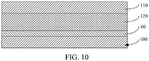
- the present disclosure further provides a liquid crystal display panel 200, the liquid crystal display panel 200 comprises the array substrate 100, a color film substrate 110 facing the array substrate 100, and a liquid crystal layer 120 provided between the array substrate 100 and the color film substrate 120.
- the alignment layer 60 of the array substrate 100 contacts with the liquid crystal layer 120, and liquid crystal molecules in the liquid crystal layer 120 are pre-aligned by the alignment layer 60.
- the present disclosure provides the array substrate and the manufacturing method thereof, a plurality of drainage grooves 52 provided at intervals on an edge of the via hole 51 through the interval layer 30, so that when the pixel electrode layer 40 is stacked on the interval layer 30, forming the groove 41 of same size of the via hole 51 corresponding to the position of the via hole 51 by the pixel electrode layers 40, and forming the sub-drainage groove 42 of same size of the drainage groove 52 corresponding to the position of each drainage groove 52.
- the alignment liquid for forming the alignment layer 60 can flow into the groove on the pixel electrode 40 through the sub-drainage groove 42, so that the position of the groove 41 on the pixel electrode layer 40 can also cover the alignment film 60, so as to ensure the normal display of the liquid crystal display panel 200 formed by the array substrate 100.
Landscapes
- Physics & Mathematics (AREA)
- Nonlinear Science (AREA)
- Mathematical Physics (AREA)
- Chemical & Material Sciences (AREA)
- Crystallography & Structural Chemistry (AREA)
- General Physics & Mathematics (AREA)
- Optics & Photonics (AREA)
- Engineering & Computer Science (AREA)
- Microelectronics & Electronic Packaging (AREA)
- Spectroscopy & Molecular Physics (AREA)
- Geometry (AREA)
- Manufacturing & Machinery (AREA)
- Liquid Crystal (AREA)
- Devices For Indicating Variable Information By Combining Individual Elements (AREA)
Abstract
Description
- The present application is a National Phase of International Application Number
PCT/CN2018/071559, filed January 5, 2018 201710934432.3, filed September 28, 2017 - The disclosure relates to a display panel manufacturing technical field, and more particularly to an array substrate, a manufacturing method of an array substrate, and a liquid crystal display panel.
- Due to its small size, low power consumption and no radiation, a liquid crystal display panel (LCD) has drawn great attention in a field of a flat panel display and has been widely applied to all walks of life. The liquid crystal display panel is usually made of a color film substrate and an array substrate. Wherein the array substrate generally comprises a source-drain layer, an interval layer disposed on the source-drain layer, and a pixel electrode layer disposed on the interval layer. Wherein a via hole needs to be disposed on the interval layer so that the pixel electrode layer is electrically connected to the source-drain layer through the via hole so as to drive and display the liquid crystal display panel. When the pixel electrode is electrically connected to the source-drain through the via hole, a groove is formed on the pixel electrode layer corresponding to a position of the via hole. Wherein since an area of the via hole is smaller so that an alignment film is subsequently disposed on the pixel electrode layer, bubbles are likely to be generated in a groove, so that an alignment liquid for forming the alignment film does not easily enter the groove of the pixel electrode layer and is evenly dispersed in the groove; therefore, an alignment film is lacking in the area, so that a display abnormality occurs in the liquid crystal display panel.
- The present disclosure provides an array substrate, a manufacturing method of an array substrate, and a liquid crystal display panel, so that each position of a pixel electrode layer of the array substrate can be covered with an alignment film to ensure normal display of the liquid crystal display panel formed by the array substrate.
- The array substrate comprises a substrate, a source-drain layer stacked on the substrate, the pixel electrode layer disposed on the source-drain layer, and an interval layer stacked between the source-drain layer and the pixel electrode layer; wherein the interval layer comprises a via hole structure, the via hole structure comprises a via hole and a plurality of drainage grooves provided at intervals on an edge of the via hole, the drainage groove is recessed in a direction from an inner wall of the via hole away from the inner portion of the via hole, the via hole has a first hole and a second hole opposite to the first hole, and the drainage groove extends from the first hole to the second hole; the pixel electrode layer is electrically connected to the source-drain layer through the via hole structure.
- Wherein an angle between an extending direction of the drainage groove and an axial direction of the via hole is the same as the angle between the inner wall of the via hole and the axial direction.
- Wherein the pixel electrode layer forms a groove corresponding to a position of the via hole, and the pixel electrode layer forms a sub-drainage groove corresponding to the position of each drainage groove.
- Wherein the array substrate further comprises an alignment layer, and the alignment layer covers the pixel electrode layer.
- The manufacturing method of the array substrate comprises steps of:
- Forming the source-drain layer on the substrate by a patterning process;
- Forming the interval layer on the source-drain layer and forming the via hole structure on the interval layer by the patterning process, wherein the via hole structure comprises the via hole and the plurality of drainage grooves provided at intervals on the edge of the via hole, the drainage groove is recessed in a direction from the inner wall of the via hole away from the inner portion of the via hole, the via hole has the first hole and the second hole opposite to the first hole, and the drainage groove extends from the first hole to the second hole; the angle between the extending direction of the drainage groove and the axial direction of the via hole is the same as or different from the angle between the inner wall of the via hole and the axial direction;
- Forming the pixel electrode layer on the interval layer, and electrically connecting the pixel electrode layer to the source-drain layer through the via hole structure, wherein the pixel electrode layer forms the groove of same size of the via hole corresponding to the position of the via hole, and forms a sub-drainage groove of same size of the drainage groove corresponding to the position of each drainage groove; and
- Covering the alignment layer on the pixel electrode layer, covering the pixel electrode layer, the inner wall of the groove and the inner wall of the sub-drainage groove of the pixel electrode layer.
- Wherein "forming the via hole structure on the interval layer by the patterning process" comprises the steps of:
- Sequentially forming an interval material layer and a photoresist material layer on the source-drain layer;
- Transferring a via pattern on a photomask to the photoresist material layer by exposing and developing the photoresist material layer through the photomask, wherein the via hole pattern on the photomask is the same size as the via hole structure;
- Etching the interval material layer, and transferring the via hole pattern formed on the photoresist material layer to the interval material layer to acquire the interval layer having the via hole structure; and
- Peeling off the photoresist layer.
- Wherein the angle between the extending direction of the drainage groove and the axial direction of the via hole is the same as the angle between the inner wall of the via hole and the axial direction, the photomask comprises a light-shielding area, a light-transmitting area and a plurality of semi-light-transmitting areas, the plurality of semi-light-transmitting areas surround the light-transmitting area and are arranged at intervals, the semi-transmitting areas are connected to the light-transmitting area, and a light transmittance of the semi-light-transmitting area gradually increases from a direction away from the light-transmitting area towards the direction of the light-transmitting area; the via hole is formed corresponding to the position of the light-transmitting area on the interval layer, and the drainage groove is formed corresponding to the position of the semi-light-transmitting area.
- Wherein when the angle between the extending direction of the drainage groove and the axial direction of the via hole is different from the angle between the inner wall of the via hole and the axial direction, the photomask comprises the light-shielding area, a first light-transmitting area and a plurality of second light-transmitting areas, the plurality of second light-transmitting areas surround the first light-transmitting area and are arranged at intervals, and the second light-transmitting areas are connected to the first light-transmitting area; the via hole is formed corresponding to the position of the first light-transmitting area on the interval layer, and the drainage groove is formed corresponding to the position of the second light-transmitting area.
- Wherein the step of "forming the alignment layer covering the pixel electrode layer on the pixel electrode layer, covering the pixel electrode layer, the inner wall of the groove and the inner wall of the sub-drainage groove of the pixel electrode layer" comprises the steps:
- Printing an alignment liquid on the pixel electrode layer and covering the pixel electrode layer, and flowing the alignment liquid into the groove along the sub-drainage groove and attaching to the inner wall of the groove and the sub-drainage groove;
- Pre-baking the alignment liquid of the inner wall on the pixel electrode layer, the groove and the sub-drainage groove to acquire the alignment layer covering the pixel electrode layer, the inner wall of the groove and the sub-drainage groove.
- The liquid crystal display panel includes the array substrate, a color film substrate facing the array substrate, and a liquid crystal layer sandwiched between the array substrate and the color film substrate, the pixel electrode layer of the array substrate facing the liquid crystal layer.
- The present disclosure provides the array substrate, the manufacturing method of the array substrate and the liquid crystal display panel, the plurality of drainage grooves provided at intervals on the edge of the via hole, when the pixel electrode layer stacked on the interval layer, forming the groove of same size of the via hole corresponding to the position of the via hole by the pixel electrode layers, and forming the sub-drainage groove of same size of the drainage groove corresponding to the position of each drainage groove.
- Furthermore, when the alignment layer is disposed on the pixel electrode, the alignment liquid for forming the alignment layer can flow into the groove on the pixel electrode through the sub-drainage groove, so that the position of the groove on the pixel electrode layer can also cover the alignment film, so as to ensure the normal display of the liquid crystal display panel formed by the array substrate.
- To describe the technical solutions in the embodiments of the present disclosure or in the prior art more clearly, the following briefly introduces the accompanying figures required for describing the embodiments or the prior art, apparently, the accompanying figures in the following description show merely some embodiments of the present disclosure, and a person of ordinary skill in the art may still derive other drawings from these accompanying figures without creative efforts.
-
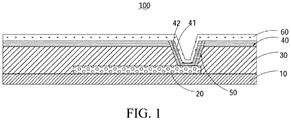
FIG. 1 is a cross-sectional schematic view of an array substrate according to an embodiment of the present disclosure; -
FIG. 2 is a structural schematic view of a via hole of an array substrate ofFIG. 1 ; -
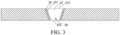
FIG. 3 is a cross-sectional schematic view of a via hole of an array substrate ofFIG. 2 ; -
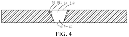
FIG. 4 is a cross-sectional schematic view of a via hole of an array substrate according to another embodiment of the present disclosure; -
FIG. 5 is a schematic flow chart of manufacturing an array substrate according to an embodiment of the present disclosure; -
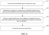
FIG. 6 is a specific flow chart ofstep 120 in a manufacturing process as shown inFIG. 3 ; -
FIG. 7 is a specific flow chart ofstep 140 in a manufacturing process as shown inFIG. 3 ; -
FIG. 8 is a structural schematic view of a light-shielding mask of a via structure on an array substrate as shown inFIG. 3 ; -
FIG. 9 is a structural schematic view of a light-shielding mask of a via structure on an array substrate as shown inFIG. 4 ; and -
FIG. 10 is a schematic view of a liquid crystal display panel according to an embodiment of the present disclosure. - The technical solutions in the embodiments of the present disclosure will be described clearly and completely hereinafter with reference to the accompanying figures in the embodiments of the present disclosure, apparently, the described embodiments are merely some but not all embodiments of the present disclosure. All other embodiments obtained by a person of ordinary skill in the art based on the embodiments of the present disclosure without creative efforts shall fall within the protection scope of the present disclosure.
- See
FIG. 1 , the present disclosure provides anarray substrate 100. Thearray substrate 100 comprises asubstrate 10, a source-drain layer 20 stacked on thesubstrate 10, apixel electrode layer 40 disposed on the source-drain layer 20, and aninterval layer 30 stacked between the source-drain layer 20 and thepixel electrode layer 40; wherein theinterval layer 30 comprises avia hole structure 50, thepixel electrode layer 40 is electrically connected to the source-drain layer 20 through thevia hole structure 50. In this embodiment, theinterval layer 30 comprises an insulating layer and a planarization layer. It may be understood that theinterval layer 30 may further comprise other layer structures according to a design requirement of thearray substrate 100. - See
FIG. 2 andFIG. 3 , thevia structure 50 comprises thevia hole 51 and a plurality ofdrainage grooves 52 provided at intervals on an edge of thevia hole 51, a liquid can flow smoothly into thevia hole 51 through the plurality ofdrainage grooves 52. Wherein a flowing direction of the liquid is an extending direction of thedrainage groove 52. Thedrainage groove 52 is recessed from in a direction aninner wall 511 of thevia hole 51 away from the inner portion of thevia hole 51. And thevia hole 51 has afirst hole 512 and asecond hole 513 opposite to thefirst hole 512. Thedrainage groove 52 extends from thefirst hole 512 to thesecond hole 513, that is, the liquid can flow from one end of thefirst hole 512 to thesecond hole 513 through thedrainage groove 52, so that the liquid can smoothly flow into the hole. In this embodiment, an angle between an extending direction of thedrainage groove 52 and an axial direction of the via hole is the same as the angle between theinner wall 511 of the via hole and the axial direction, and thedrainage groove 52 extends from an end of thefirst hole 512 to the end of thesecond hole 513. SeeFIG. 4 , in the other embodiment of the present disclosure, the angle between the axial direction of theliquid guiding groove 52 and theinner wall 511 of the via hole is different from the angle of the axial direction. In addition, it can be understood that thedrainage groove 52 may not extend to one end of thesecond hole 513, and thedrainage groove 52 can still achieve an effect of guiding the liquid into thevia hole 51. In addition, thedrainage groove 52 may have any shape, for example, thedrainage groove 52 may be V-shaped, semicircular, parabolic and so on. - The
pixel electrode layer 40 is stacked on theinterval layer 30, and thegroove 41 is formed at the position corresponding to thevia hole 51, the inner wall of thegroove 41 has the same size as the inner wall of thevia hole 51. Thesub-drainage groove 42 is formed at the position corresponding to eachdrainage grooves 52, and the inner wall of thesub-drainage groove 42 has the same size as the inner wall of thedrainage groove 52. - Further, the
array substrate 100 comprises analignment layer 60, and thealignment layer 60 covers thepixel electrode layer 40, that is thealignment layer 60 can cover the inner wall of thegroove 41 and thesub-drainage groove 42. Specifically, an alignment liquid for forming thealignment layer 60 can flow into thegroove 41 through thesub-drainage groove 42, and bubbles are not easily generated in thegroove 41 due to a surface of the alignment liquid, so that thealignment layer 60 can be covered and evenly dispersed in thegroove 41 and thealignment layer 60 can cover any position of thepixel electrode layer 40. - See
FIG. 5 , the present disclosure further provides a manufacturing method of array substrate, comprising: -
Step 110, forming the source-drain layer 20 on thesubstrate 10 by a patterning process. Specifically, the patterning process comprises the steps of a photoresist coating, an exposure, a development, an etching and so on, the source-drain layer 20 formed by the patterning process comprises source electrode and drain electrode disposed at intervals. -
Step 120, forming theinterval layer 30 on the source-drain layer 20 and forming the viahole structure 50 on theinterval layer 30 by the patterning process. The structure of the viahole structure 50 has been described, which will not be repeated here. - See
FIG. 6 , thestep 120 further comprises:
An interval material layer is formed on the source-drain layer. The interval material layer is formed on the source-drain layer 20 by a vapor deposition and a coating and so on. In this embodiment, theinterval layer 30 comprises an insulating layer and a planarization layer stacked on the insulating layer. The insulating layer is stacked and covered on the source-drain layer 20 by the vapor deposition; and the planarization layer is formed on the insulating layer by coating. Afterwards, a photoresist material layer is formed on the interval material layer by the coating process. -
Step 122, the photoresist material layer is exposed and developed through aphotomask 70 to transfer the via hole pattern on thephotomask 70 on the photoresist material layer. The via hole pattern on thephotomask 70 is the same size as the via hole structure. Specifically, a pattern on the photomask is also different according to different via hole structure. - See
FIG. 3 andFIG. 8 , in this embodiment, thedrainage groove 52 is parallel to the axial direction of the via hole. The photomask comprises the light-shieldingarea 74, a first light-transmittingarea 76 and a plurality of second light-transmittingareas 75, the plurality of second light-transmittingareas 75 surround the first light-transmittingarea 76 and are arranged at intervals, and thesecond transmitting areas 75 are connected to the first light-transmittingarea 76. A portion of thephotomask 70 other than the first light-transmittingarea 76 and the second light-transmittingarea 75 is the light-shieldingarea 74. Wherein forming the viahole 51 corresponding to the position of the first light-transmittingarea 76 on theinterval layer 30, and forming thedrainage groove 52 corresponding to the position of the second light-transmittingarea 75. - Alternatively, see
FIG. 4 andFIG. 9 , in other embodiments of the present disclosure, when the angle is formed between thedrainage groove 52 of the viastructure 10 and the inner wall of the via hole 111, thephotomask 70 comprises the light-shieldingarea 71, a light-transmittingarea 73 and a plurality of semi-light-transmittingareas 72. The semi-light-transmittingarea 72 surround the light-transmittingarea 73 and are arranged at intervals, and thesemi-transmitting area 72 is connected to the light-transmittingarea 73, and a light transmittance of the semi-light-transmittingarea 72 gradually increases from a direction away from the light-transmittingarea 73 towards the direction of the light-transmittingarea 73. The portion of thephotomask 70 other than the light-transmittingarea 73 and the semi-light-transmittingarea 72 is the light-shieldingarea 71. Wherein the via hole 11 is formed on theinterval layer 30 corresponding to the position of the light-transmittingarea 73, and the drainage groove 12 is formed corresponding to the position of the light-transmittingarea 72. In addition, since the light transmittance of the semi-light-transmittingarea 72 gradually increases from the direction away from the light-transmittingarea 73 toward the light-transmittingarea 73, an etching depth corresponding to thesemi-transmitting area 72 is gradually changed, so that the angle is formed between thedrainage groove 52 and the inner wall of the viahole 51. Transferring the via pattern on thephotomask 70 to the photoresist material layer specifically comprises providing thephotomask 70 on the photoresist material layer, the photoresist material layer is exposed and developed by thephotomask 70 to transfer the via pattern on thephotomask 70 to the photoresist material layer. -
Step 123, etching the interval material layer, and transferring the via pattern formed on the photoresist material layer to the interval material layer to acquire theinterval layer 30 with the viastructure 50. -
Step 124, peeling off the photoresist material layer. After etching the interval material layer is completed and theinterval layer 30 with the viahole structure 50 is formed, the photoresist material layer can be peeled off. -
Step 130, forming thepixel electrode layer 40 on theinterval layer 30, and electrically connecting thepixel electrode layer 40 to the source-drain layer 20 through the viahole structure 50, forming thegroove 41 of same size of the via hole corresponding to the position of the viahole 51 by the pixel electrode layers 40, and forming thesub-drainage groove 42 of same size of thedrainage groove 52 corresponding to the position of eachdrainage groove 52. In this embodiment, thepixel electrode layer 40 is formed on theinterval layer 30 by the vapor deposition. -
Step 140, covering analignment layer 60 on thepixel electrode layer 40, thealignment layer 60 covering thepixel electrode layer 40, the inner wall of thegroove 41 and the inner wall of thesub-drainage groove 42 of thepixel electrode layer 40. - Specifically, see
FIG. 7 , step 140 further comprises: -
Step 141, printing an alignment liquid on thepixel electrode layer 40 and covering thepixel electrode layer 40, and flowing the alignment liquid into thegroove 41 along thesub-drainage groove 42 and attaching to thegroove 41 and the inner wall of thesub-drainage groove 42. The alignment liquid is easily to flow into thegroove 41 through thesub-drainage groove 42, so as to avoid to generate the bubbles in thegroove 41, so that the alignment liquid can enter thegrooves 41 of the pixel electrode layer and evenly disperse in thegrooves 41, the alignment liquid can be evenly distributed at each position of thepixel electrode layer 40. -
Step 142, pre-baking the alignment liquid of the inner wall on thesub-drainage groove 42, thegroove 41 of thepixel electrode layer 40 and thepixel electrode layer 40 to acquire thealignment layer 60 covering thepixel electrode layer 42, the inner wall of thegroove 41 of thepixel electrode layer 40 and the inner wall of thesub-drainage groove 42. - See
FIG. 10 , the present disclosure further provides a liquid crystal display panel 200, the liquid crystal display panel 200 comprises thearray substrate 100, acolor film substrate 110 facing thearray substrate 100, and aliquid crystal layer 120 provided between thearray substrate 100 and thecolor film substrate 120. Thealignment layer 60 of thearray substrate 100 contacts with theliquid crystal layer 120, and liquid crystal molecules in theliquid crystal layer 120 are pre-aligned by thealignment layer 60. - The present disclosure provides the array substrate and the manufacturing method thereof, a plurality of
drainage grooves 52 provided at intervals on an edge of the viahole 51 through theinterval layer 30, so that when thepixel electrode layer 40 is stacked on theinterval layer 30, forming thegroove 41 of same size of the viahole 51 corresponding to the position of the viahole 51 by the pixel electrode layers 40, and forming thesub-drainage groove 42 of same size of thedrainage groove 52 corresponding to the position of eachdrainage groove 52. Furthermore, when thealignment layer 60 is disposed on thepixel electrode 40, the alignment liquid for forming thealignment layer 60 can flow into the groove on thepixel electrode 40 through thesub-drainage groove 42, so that the position of thegroove 41 on thepixel electrode layer 40 can also cover thealignment film 60, so as to ensure the normal display of the liquid crystal display panel 200 formed by thearray substrate 100. - The foregoing disclosure is merely a preferred embodiment of the present disclosure, and certainly can not be used to limit the scope of the present disclosure, persons of ordinary skill in the art may understand that all or part of the procedures for implementing the foregoing embodiments and equivalent changes made according to the claims of the present disclosure still fall within the scope of the present disclosure.
Claims (13)
- An array substrate, comprising a substrate, a source-drain layer stacked on the substrate, a pixel electrode layer disposed on the source-drain layer, and an interval layer stacked between the source-drain layer and the pixel electrode layer; wherein the interval layer comprises a via hole structure, the via hole structure comprises a via hole and a plurality of drainage grooves provided at intervals on an edge of the via hole, the drainage groove is recessed in a direction from an inner wall of the via hole away from the inner portion of the via hole, the via hole has a first hole and a second hole opposite to the first hole, and the drainage groove extends from the first hole to the second hole; the pixel electrode layer is electrically connected to the source-drain layer through the via hole structure.
- The array substrate according to claim 1, wherein an angle between an extending direction of the drainage groove and an axial direction of the via hole is the same as the angle between the inner wall of the via hole and the axial direction.
- The array substrate according to claim 1, wherein the pixel electrode layer forms a groove corresponding to a position of the via hole, and the pixel electrode layer forms a sub-drainage groove corresponding to the position of each drainage groove.
- The array substrate according to claim 1, wherein the array substrate further comprises an alignment layer, and the alignment layer covers the pixel electrode layer.
- A manufacturing method of an array substrate, comprising steps of:forming a source-drain layer on a substrate by a patterning process;forming an interval layer on the source-drain layer and forming a via hole structure on the interval layer by the patterning process, wherein the via hole structure comprises a via hole and a plurality of drainage grooves provided at intervals on an edge of the via hole, the drainage groove is recessed in a direction from an inner wall of the via hole away from the inner portion of the via hole, the via hole has a first hole and a second hole opposite to the first hole, and the drainage groove extends from the first hole to the second hole; an angle between an extending direction of the drainage groove and an axial direction of the via hole is the same as or different from the angle between the inner wall of the via hole and the axial direction;forming a pixel electrode layer on the interval layer, and electrically connecting the pixel electrode layer to the source-drain layer through the via hole structure, wherein the pixel electrode layer forms a groove of same size of the via hole corresponding to a position of the via hole, and forms a sub-drainage groove of same size of the drainage groove corresponding to the position of each drainage groove; andcovering an alignment layer on the pixel electrode layer, the alignment layer covering the pixel electrode layer, the inner wall of the groove and the inner wall of the sub-drainage groove of the pixel electrode layer.
- The manufacturing method of an array substrate according to claim 5, wherein "forming the via hole structure on the interval layer by the patterning process" comprises the steps of:sequentially forming an interval material layer and a photoresist material layer on the source-drain layer;transferring a via pattern on a photomask to the photoresist material layer by exposing and developing the photoresist material layer through the photomask, wherein a via hole pattern on the photomask is the same size as the via hole structure;etching the interval material layer, and transferring the via hole pattern formed on the photoresist material layer to the interval material layer to acquire the interval layer having the via hole structure; andpeeling off the photoresist material layer.
- The manufacturing method of an array substrate according to claim 6, wherein the angle between the extending direction of the drainage groove and the axial direction of the via hole is the same as the angle between the inner wall of the via hole and the axial direction, the photomask comprises a light-shielding area, a light-transmitting area and a plurality of semi-light-transmitting areas, the plurality of semi-light-transmitting areas surround the light-transmitting area and are arranged at intervals, the semi-transmitting areas are connected to the light-transmitting area, and a light transmittance of the semi-light-transmitting area gradually increases from a direction away from the light-transmitting area towards the direction of the light-transmitting area; the via hole is formed corresponding to the position of the light-transmitting area on the interval layer, and the drainage groove is formed corresponding to the position of the semi-light-transmitting area.
- The manufacturing method of an array substrate according to claim 6, wherein when the angle between the extending direction of the drainage groove and the axial direction of the via hole is different from the angle between the inner wall of the via hole and the axial direction, the photomask comprises the light-shielding area, a first light-transmitting area and a plurality of second light-transmitting areas, the plurality of second light-transmitting areas surround the first light-transmitting area and are arranged at intervals, and the second light-transmitting areas are connected to the first light-transmitting area; the via hole is formed corresponding to the position of the first light-transmitting area on the interval layer, and the drainage groove is formed corresponding to the position of the second light-transmitting area.
- The manufacturing method of an array substrate according to claim 5, wherein the step of "forming the alignment layer covering the pixel electrode layer on the pixel electrode layer, covering the pixel electrode layer, the inner wall of the groove and the inner wall of the sub-drainage groove of the pixel electrode layer" comprises the steps:printing an alignment liquid on the pixel electrode layer and covering the pixel electrode layer, and flowing the alignment liquid into the groove along the sub-drainage groove and attaching to the inner wall of the groove and the sub-drainage groove;pre-baking the alignment liquid of the inner wall on the pixel electrode layer, the groove and the sub-drainage groove to acquire the alignment layer covering the pixel electrode layer, the inner wall of the groove and the sub-drainage groove.
- A liquid crystal display panel, comprising an array substrate, a color film substrate facing the array substrate, and a liquid crystal layer sandwiched between the array substrate and the color film substrate; wherein the e array substrate comprises a substrate, a source-drain layer stacked on the substrate, a pixel electrode layer provided on the source-drain layer, and an interval layer stacked between the source-drain layer and the pixel electrode layer, the interval layer comprises a via hole structure, the via hole structure comprises a via hole and a plurality of drainage grooves provided at intervals on an edge of the via hole, the drainage groove is recessed from an inner wall of the via hole in a direction away from the inner portion of the via hole, the via hole has a first hole and the first hole opposite to a second hole, and the drainage groove extends from the first hole to the second hole; the pixel electrode layer is electrically connected to the source-drain layer through the via hole structure.
- The liquid crystal display panel according to claim 10, wherein an angle between an extending direction of the drainage groove and an axial direction of the via hole is the same as the angle between the inner wall of the via hole and the axial direction.
- The liquid crystal display panel according to claim 10, wherein the pixel electrode layer forms a groove corresponding to a position of the via hole, and forms a sub-drainage groove corresponding to the position of each drainage groove.
- The liquid crystal display panel according to claim 10, wherein array substrate further comprises an alignment layer, and the alignment layer covers the pixel electrode layer.
Applications Claiming Priority (2)
| Application Number | Priority Date | Filing Date | Title |
|---|---|---|---|
| CN201710934432.3A CN107479292B (en) | 2017-09-28 | 2017-09-28 | Array substrate, manufacturing method of array substrate, and liquid crystal display panel |
| PCT/CN2018/071559 WO2019061937A1 (en) | 2017-09-28 | 2018-01-05 | Array substrate, manufacturing method for the array substrate and liquid crystal display panel |
Publications (3)
| Publication Number | Publication Date |
|---|---|
| EP3690536A1 true EP3690536A1 (en) | 2020-08-05 |
| EP3690536A4 EP3690536A4 (en) | 2021-06-16 |
| EP3690536B1 EP3690536B1 (en) | 2025-05-28 |
Family
ID=60606042
Family Applications (1)
| Application Number | Title | Priority Date | Filing Date |
|---|---|---|---|
| EP18862214.6A Active EP3690536B1 (en) | 2017-09-28 | 2018-01-05 | Array substrate, manufacturing method for the array substrate and liquid crystal display panel |
Country Status (6)
| Country | Link |
|---|---|
| US (1) | US10620496B2 (en) |
| EP (1) | EP3690536B1 (en) |
| JP (1) | JP6985507B2 (en) |
| KR (1) | KR20200054316A (en) |
| CN (1) | CN107479292B (en) |
| WO (1) | WO2019061937A1 (en) |
Families Citing this family (14)
| Publication number | Priority date | Publication date | Assignee | Title |
|---|---|---|---|---|
| CN107479292B (en) | 2017-09-28 | 2020-08-04 | 武汉华星光电技术有限公司 | Array substrate, manufacturing method of array substrate, and liquid crystal display panel |
| CN108227323B (en) * | 2017-12-29 | 2021-05-11 | Tcl华星光电技术有限公司 | COA substrate and photomask for making vias in resin layer of COA substrate |
| CN109116646A (en) * | 2018-09-07 | 2019-01-01 | 深圳市华星光电技术有限公司 | A kind of array substrate, display panel and light shield |
| CN110061012B (en) * | 2019-04-09 | 2022-01-28 | Tcl华星光电技术有限公司 | Array substrate, manufacturing method thereof and display panel |
| CN109976017B (en) * | 2019-04-10 | 2021-09-24 | 深圳市华星光电半导体显示技术有限公司 | Display panel and manufacturing method thereof |
| US11081537B2 (en) | 2019-08-15 | 2021-08-03 | Tcl China Star Optoelectronics Technology Co., Ltd. | Substrate and manufacturing method thereof |
| CN110568640B (en) * | 2019-08-15 | 2021-03-23 | Tcl华星光电技术有限公司 | Substrate and manufacturing method thereof |
| US11194196B2 (en) * | 2019-12-18 | 2021-12-07 | Tcl China Star Optoelectronics Technology Co., Ltd. | Array substrate and liquid crystal display panel |
| CN110928093B (en) * | 2019-12-18 | 2021-08-24 | Tcl华星光电技术有限公司 | Array substrate and liquid crystal display panel |
| EP4170418B1 (en) | 2020-09-29 | 2025-10-29 | BOE Technology Group Co., Ltd. | Array substrate |
| CN112363357A (en) * | 2020-12-03 | 2021-02-12 | 深圳市华星光电半导体显示技术有限公司 | Array substrate and display panel |
| CN113156714B (en) * | 2021-04-28 | 2023-12-08 | Tcl华星光电技术有限公司 | Array substrate and liquid crystal display panel |
| US11506946B1 (en) | 2021-04-28 | 2022-11-22 | Tcl China Star Optoelectronics Technology Co., Ltd. | Array substrate and liquid crystal display panel |
| CN119225074B (en) * | 2024-08-30 | 2026-03-03 | 惠科股份有限公司 | Methods for manufacturing display panels, display panels and display devices |
Family Cites Families (11)
| Publication number | Priority date | Publication date | Assignee | Title |
|---|---|---|---|---|
| KR101893939B1 (en) * | 2011-08-26 | 2018-08-31 | 엘지디스플레이 주식회사 | Contact structure of line and LCD including the same |
| WO2014103922A1 (en) * | 2012-12-27 | 2014-07-03 | シャープ株式会社 | Display element, display device, and method for manufacturing display element |
| JP6073928B2 (en) * | 2012-12-27 | 2017-02-01 | シャープ株式会社 | Display element |
| CN203630483U (en) * | 2013-12-30 | 2014-06-04 | 厦门天马微电子有限公司 | Array substrate and liquid crystal display |
| TWI553881B (en) * | 2014-06-06 | 2016-10-11 | 群創光電股份有限公司 | Thin film transistor substrate |
| CN104345485A (en) * | 2014-11-10 | 2015-02-11 | 深圳市华星光电技术有限公司 | Liquid crystal display panel and through hole for electrical connection |
| CN204331229U (en) * | 2014-12-03 | 2015-05-13 | 京东方科技集团股份有限公司 | Liquid crystal display |
| KR102340409B1 (en) * | 2015-05-12 | 2021-12-17 | 삼성디스플레이 주식회사 | Display device |
| CN105355630A (en) * | 2015-10-10 | 2016-02-24 | 深圳市华星光电技术有限公司 | Array substrate and liquid crystal display including same |
| CN106950769B (en) * | 2017-03-20 | 2020-05-05 | 深圳市华星光电技术有限公司 | Array substrate, display device |
| CN107479292B (en) * | 2017-09-28 | 2020-08-04 | 武汉华星光电技术有限公司 | Array substrate, manufacturing method of array substrate, and liquid crystal display panel |
-
2017
- 2017-09-28 CN CN201710934432.3A patent/CN107479292B/en active Active
-
2018
- 2018-01-05 JP JP2020517792A patent/JP6985507B2/en active Active
- 2018-01-05 KR KR1020207012411A patent/KR20200054316A/en not_active Ceased
- 2018-01-05 WO PCT/CN2018/071559 patent/WO2019061937A1/en not_active Ceased
- 2018-01-05 EP EP18862214.6A patent/EP3690536B1/en active Active
- 2018-03-09 US US15/916,380 patent/US10620496B2/en active Active
Also Published As
| Publication number | Publication date |
|---|---|
| KR20200054316A (en) | 2020-05-19 |
| CN107479292A (en) | 2017-12-15 |
| EP3690536A4 (en) | 2021-06-16 |
| US20190094638A1 (en) | 2019-03-28 |
| CN107479292B (en) | 2020-08-04 |
| WO2019061937A1 (en) | 2019-04-04 |
| JP6985507B2 (en) | 2021-12-22 |
| EP3690536B1 (en) | 2025-05-28 |
| US10620496B2 (en) | 2020-04-14 |
| JP2020535480A (en) | 2020-12-03 |
Similar Documents
| Publication | Publication Date | Title |
|---|---|---|
| US10620496B2 (en) | Array substrate, manufacturing method of array substrate and liquid crystal display panel | |
| CN105514125B (en) | A kind of array substrate, preparation method and display panel | |
| TWI515910B (en) | Thin film transistor substrate, manufacturing method thereof, and display | |
| US20160306241A1 (en) | Array substrate and its manufacturing method and display device | |
| KR102057821B1 (en) | Liquid Crystal Display Panel, Array Substrate and Manufacturing Method Thereof | |
| US11189641B2 (en) | Method for manufacturing array substrate, array substrate and display apparatus | |
| US9166097B2 (en) | Thin film transistor substrate and manufacturing method thereof, display | |
| EP3091568B1 (en) | Array substrate, manufacturing method therefor, display device and electronic product | |
| US20150303225A1 (en) | Array substrate, fabrication method thereof and display device | |
| WO2016123931A1 (en) | Thin film transistor and manufacturing method thereof, display substrate and display device | |
| TW201418855A (en) | Array substrate of display panel and manufacturing method thereof | |
| US20150313021A1 (en) | Display panel motherboard and manufacturing method thereof | |
| US9057923B2 (en) | Wire, method of manufacture, and related apparatus | |
| KR101467710B1 (en) | Tft array substrate, manufacturing method of the same and display device | |
| US20160011457A1 (en) | Fabrication method of substrate | |
| US12159885B2 (en) | Manufacturing method of mini-LED backlight plate and mini-LED backlight plate | |
| EP3343623B1 (en) | Array substrate, manufacturing method thereof and display panel | |
| US20160109739A1 (en) | Manufacturing method of tft array substrate, tft array substrate and display device | |
| US20150021611A1 (en) | Array substrate and manufacturing method thereof | |
| CN106024908A (en) | Thin film transistor fabrication method and array substrate fabrication method | |
| CN105428368A (en) | Film transistor array substrate and preparation method thereof, and display device | |
| KR102098012B1 (en) | Liquid crystal display device | |
| US20080024702A1 (en) | Pixel structure and fabrication method thereof | |
| US10714513B2 (en) | Array substrate and manufacturing method thereof, liquid crystal display device and manufacturing method thereof | |
| KR102113601B1 (en) | Thin film transistor array substrate and method for manufacturing the same |
Legal Events
| Date | Code | Title | Description |
|---|---|---|---|
| STAA | Information on the status of an ep patent application or granted ep patent |
Free format text: STATUS: THE INTERNATIONAL PUBLICATION HAS BEEN MADE |
|
| PUAI | Public reference made under article 153(3) epc to a published international application that has entered the european phase |
Free format text: ORIGINAL CODE: 0009012 |
|
| STAA | Information on the status of an ep patent application or granted ep patent |
Free format text: STATUS: REQUEST FOR EXAMINATION WAS MADE |
|
| 17P | Request for examination filed |
Effective date: 20200420 |
|
| AK | Designated contracting states |
Kind code of ref document: A1 Designated state(s): AL AT BE BG CH CY CZ DE DK EE ES FI FR GB GR HR HU IE IS IT LI LT LU LV MC MK MT NL NO PL PT RO RS SE SI SK SM TR |
|
| AX | Request for extension of the european patent |
Extension state: BA ME |
|
| DAV | Request for validation of the european patent (deleted) | ||
| DAX | Request for extension of the european patent (deleted) | ||
| A4 | Supplementary search report drawn up and despatched |
Effective date: 20210517 |
|
| RIC1 | Information provided on ipc code assigned before grant |
Ipc: G02F 1/1337 20060101AFI20210510BHEP Ipc: H01L 27/12 20060101ALI20210510BHEP Ipc: G02F 1/1362 20060101ALI20210510BHEP |
|
| STAA | Information on the status of an ep patent application or granted ep patent |
Free format text: STATUS: EXAMINATION IS IN PROGRESS |
|
| 17Q | First examination report despatched |
Effective date: 20240417 |
|
| GRAP | Despatch of communication of intention to grant a patent |
Free format text: ORIGINAL CODE: EPIDOSNIGR1 |
|
| STAA | Information on the status of an ep patent application or granted ep patent |
Free format text: STATUS: GRANT OF PATENT IS INTENDED |
|
| INTG | Intention to grant announced |
Effective date: 20250113 |
|
| GRAS | Grant fee paid |
Free format text: ORIGINAL CODE: EPIDOSNIGR3 |
|
| GRAA | (expected) grant |
Free format text: ORIGINAL CODE: 0009210 |
|
| STAA | Information on the status of an ep patent application or granted ep patent |
Free format text: STATUS: THE PATENT HAS BEEN GRANTED |
|
| AK | Designated contracting states |
Kind code of ref document: B1 Designated state(s): AL AT BE BG CH CY CZ DE DK EE ES FI FR GB GR HR HU IE IS IT LI LT LU LV MC MK MT NL NO PL PT RO RS SE SI SK SM TR |
|
| P01 | Opt-out of the competence of the unified patent court (upc) registered |
Free format text: CASE NUMBER: APP_19103/2025 Effective date: 20250422 |
|
| REG | Reference to a national code |
Ref country code: GB Ref legal event code: FG4D |
|
| REG | Reference to a national code |
Ref country code: CH Ref legal event code: EP |
|
| REG | Reference to a national code |
Ref country code: IE Ref legal event code: FG4D Ref country code: DE Ref legal event code: R096 Ref document number: 602018082309 Country of ref document: DE |
|
| REG | Reference to a national code |
Ref country code: NL Ref legal event code: MP Effective date: 20250528 |
|
| PG25 | Lapsed in a contracting state [announced via postgrant information from national office to epo] |
Ref country code: ES Free format text: LAPSE BECAUSE OF FAILURE TO SUBMIT A TRANSLATION OF THE DESCRIPTION OR TO PAY THE FEE WITHIN THE PRESCRIBED TIME-LIMIT Effective date: 20250528 Ref country code: FI Free format text: LAPSE BECAUSE OF FAILURE TO SUBMIT A TRANSLATION OF THE DESCRIPTION OR TO PAY THE FEE WITHIN THE PRESCRIBED TIME-LIMIT Effective date: 20250528 |
|
| REG | Reference to a national code |
Ref country code: LT Ref legal event code: MG9D |
|
| PG25 | Lapsed in a contracting state [announced via postgrant information from national office to epo] |
Ref country code: GR Free format text: LAPSE BECAUSE OF FAILURE TO SUBMIT A TRANSLATION OF THE DESCRIPTION OR TO PAY THE FEE WITHIN THE PRESCRIBED TIME-LIMIT Effective date: 20250829 Ref country code: NO Free format text: LAPSE BECAUSE OF FAILURE TO SUBMIT A TRANSLATION OF THE DESCRIPTION OR TO PAY THE FEE WITHIN THE PRESCRIBED TIME-LIMIT Effective date: 20250828 |
|
| PG25 | Lapsed in a contracting state [announced via postgrant information from national office to epo] |
Ref country code: PL Free format text: LAPSE BECAUSE OF FAILURE TO SUBMIT A TRANSLATION OF THE DESCRIPTION OR TO PAY THE FEE WITHIN THE PRESCRIBED TIME-LIMIT Effective date: 20250528 Ref country code: NL Free format text: LAPSE BECAUSE OF FAILURE TO SUBMIT A TRANSLATION OF THE DESCRIPTION OR TO PAY THE FEE WITHIN THE PRESCRIBED TIME-LIMIT Effective date: 20250528 |
|
| PG25 | Lapsed in a contracting state [announced via postgrant information from national office to epo] |
Ref country code: BG Free format text: LAPSE BECAUSE OF FAILURE TO SUBMIT A TRANSLATION OF THE DESCRIPTION OR TO PAY THE FEE WITHIN THE PRESCRIBED TIME-LIMIT Effective date: 20250528 |
|
| PG25 | Lapsed in a contracting state [announced via postgrant information from national office to epo] |
Ref country code: HR Free format text: LAPSE BECAUSE OF FAILURE TO SUBMIT A TRANSLATION OF THE DESCRIPTION OR TO PAY THE FEE WITHIN THE PRESCRIBED TIME-LIMIT Effective date: 20250528 |
|
| PG25 | Lapsed in a contracting state [announced via postgrant information from national office to epo] |
Ref country code: RS Free format text: LAPSE BECAUSE OF FAILURE TO SUBMIT A TRANSLATION OF THE DESCRIPTION OR TO PAY THE FEE WITHIN THE PRESCRIBED TIME-LIMIT Effective date: 20250828 |
|
| PG25 | Lapsed in a contracting state [announced via postgrant information from national office to epo] |
Ref country code: IS Free format text: LAPSE BECAUSE OF FAILURE TO SUBMIT A TRANSLATION OF THE DESCRIPTION OR TO PAY THE FEE WITHIN THE PRESCRIBED TIME-LIMIT Effective date: 20250928 |
|
| PG25 | Lapsed in a contracting state [announced via postgrant information from national office to epo] |
Ref country code: LV Free format text: LAPSE BECAUSE OF FAILURE TO SUBMIT A TRANSLATION OF THE DESCRIPTION OR TO PAY THE FEE WITHIN THE PRESCRIBED TIME-LIMIT Effective date: 20250528 |
|
| REG | Reference to a national code |
Ref country code: AT Ref legal event code: MK05 Ref document number: 1798927 Country of ref document: AT Kind code of ref document: T Effective date: 20250528 |
|
| PG25 | Lapsed in a contracting state [announced via postgrant information from national office to epo] |
Ref country code: SM Free format text: LAPSE BECAUSE OF FAILURE TO SUBMIT A TRANSLATION OF THE DESCRIPTION OR TO PAY THE FEE WITHIN THE PRESCRIBED TIME-LIMIT Effective date: 20250528 Ref country code: AT Free format text: LAPSE BECAUSE OF FAILURE TO SUBMIT A TRANSLATION OF THE DESCRIPTION OR TO PAY THE FEE WITHIN THE PRESCRIBED TIME-LIMIT Effective date: 20250528 Ref country code: DK Free format text: LAPSE BECAUSE OF FAILURE TO SUBMIT A TRANSLATION OF THE DESCRIPTION OR TO PAY THE FEE WITHIN THE PRESCRIBED TIME-LIMIT Effective date: 20250528 |
|
| PG25 | Lapsed in a contracting state [announced via postgrant information from national office to epo] |
Ref country code: CZ Free format text: LAPSE BECAUSE OF FAILURE TO SUBMIT A TRANSLATION OF THE DESCRIPTION OR TO PAY THE FEE WITHIN THE PRESCRIBED TIME-LIMIT Effective date: 20250528 |
|
| PG25 | Lapsed in a contracting state [announced via postgrant information from national office to epo] |
Ref country code: EE Free format text: LAPSE BECAUSE OF FAILURE TO SUBMIT A TRANSLATION OF THE DESCRIPTION OR TO PAY THE FEE WITHIN THE PRESCRIBED TIME-LIMIT Effective date: 20250528 |
|
| PG25 | Lapsed in a contracting state [announced via postgrant information from national office to epo] |
Ref country code: SK Free format text: LAPSE BECAUSE OF FAILURE TO SUBMIT A TRANSLATION OF THE DESCRIPTION OR TO PAY THE FEE WITHIN THE PRESCRIBED TIME-LIMIT Effective date: 20250528 Ref country code: RO Free format text: LAPSE BECAUSE OF FAILURE TO SUBMIT A TRANSLATION OF THE DESCRIPTION OR TO PAY THE FEE WITHIN THE PRESCRIBED TIME-LIMIT Effective date: 20250528 |
|
| PG25 | Lapsed in a contracting state [announced via postgrant information from national office to epo] |
Ref country code: IT Free format text: LAPSE BECAUSE OF FAILURE TO SUBMIT A TRANSLATION OF THE DESCRIPTION OR TO PAY THE FEE WITHIN THE PRESCRIBED TIME-LIMIT Effective date: 20250528 |
|
| REG | Reference to a national code |
Ref country code: DE Ref legal event code: R097 Ref document number: 602018082309 Country of ref document: DE |
|
| PLBE | No opposition filed within time limit |
Free format text: ORIGINAL CODE: 0009261 |
|
| STAA | Information on the status of an ep patent application or granted ep patent |
Free format text: STATUS: NO OPPOSITION FILED WITHIN TIME LIMIT |
|
| PGFP | Annual fee paid to national office [announced via postgrant information from national office to epo] |
Ref country code: GB Payment date: 20260123 Year of fee payment: 9 |
|
| REG | Reference to a national code |
Ref country code: CH Ref legal event code: L10 Free format text: ST27 STATUS EVENT CODE: U-0-0-L10-L00 (AS PROVIDED BY THE NATIONAL OFFICE) Effective date: 20260409 |
|
| PGFP | Annual fee paid to national office [announced via postgrant information from national office to epo] |
Ref country code: DE Payment date: 20260121 Year of fee payment: 9 |
|
| PGFP | Annual fee paid to national office [announced via postgrant information from national office to epo] |
Ref country code: FR Payment date: 20260123 Year of fee payment: 9 |
|
| 26N | No opposition filed |
Effective date: 20260303 |