EP3689816A1 - Method of manufacturing an integrated component with improved spatial occupation, and integrated component - Google Patents
Method of manufacturing an integrated component with improved spatial occupation, and integrated component Download PDFInfo
- Publication number
- EP3689816A1 EP3689816A1 EP20153241.3A EP20153241A EP3689816A1 EP 3689816 A1 EP3689816 A1 EP 3689816A1 EP 20153241 A EP20153241 A EP 20153241A EP 3689816 A1 EP3689816 A1 EP 3689816A1
- Authority
- EP
- European Patent Office
- Prior art keywords
- wafer
- substrate
- cap
- coupling
- micromirror
- Prior art date
- Legal status (The legal status is an assumption and is not a legal conclusion. Google has not performed a legal analysis and makes no representation as to the accuracy of the status listed.)
- Granted
Links
Images


Classifications
-
- H—ELECTRICITY
- H10—SEMICONDUCTOR DEVICES; ELECTRIC SOLID-STATE DEVICES NOT OTHERWISE PROVIDED FOR
- H10P—GENERIC PROCESSES OR APPARATUS FOR THE MANUFACTURE OR TREATMENT OF DEVICES COVERED BY CLASS H10
- H10P72/00—Handling or holding of wafers, substrates or devices during manufacture or treatment thereof
- H10P72/04—Apparatus for manufacture or treatment
- H10P72/0446—Apparatus for mounting on conductive members, e.g. leadframes or conductors on insulating substrates
-
- B—PERFORMING OPERATIONS; TRANSPORTING
- B81—MICROSTRUCTURAL TECHNOLOGY
- B81C—PROCESSES OR APPARATUS SPECIALLY ADAPTED FOR THE MANUFACTURE OR TREATMENT OF MICROSTRUCTURAL DEVICES OR SYSTEMS
- B81C1/00—Manufacture or treatment of devices or systems in or on a substrate
- B81C1/00015—Manufacture or treatment of devices or systems in or on a substrate for manufacturing microsystems
- B81C1/00222—Integrating an electronic processing unit with a micromechanical structure
- B81C1/00238—Joining a substrate with an electronic processing unit and a substrate with a micromechanical structure
-
- H—ELECTRICITY
- H10—SEMICONDUCTOR DEVICES; ELECTRIC SOLID-STATE DEVICES NOT OTHERWISE PROVIDED FOR
- H10F—INORGANIC SEMICONDUCTOR DEVICES SENSITIVE TO INFRARED RADIATION, LIGHT, ELECTROMAGNETIC RADIATION OF SHORTER WAVELENGTH OR CORPUSCULAR RADIATION
- H10F77/00—Constructional details of devices covered by this subclass
- H10F77/40—Optical elements or arrangements
- H10F77/407—Optical elements or arrangements indirectly associated with the devices
-
- G—PHYSICS
- G02—OPTICS
- G02B—OPTICAL ELEMENTS, SYSTEMS OR APPARATUS
- G02B1/00—Optical elements characterised by the material of which they are made; Optical coatings for optical elements
- G02B1/02—Optical elements characterised by the material of which they are made; Optical coatings for optical elements made of crystals, e.g. rock-salt, semi-conductors
-
- G—PHYSICS
- G02—OPTICS
- G02B—OPTICAL ELEMENTS, SYSTEMS OR APPARATUS
- G02B26/00—Optical devices or arrangements for the control of light using movable or deformable optical elements
- G02B26/08—Optical devices or arrangements for the control of light using movable or deformable optical elements for controlling the direction of light
- G02B26/0816—Optical devices or arrangements for the control of light using movable or deformable optical elements for controlling the direction of light by means of one or more reflecting elements
- G02B26/0833—Optical devices or arrangements for the control of light using movable or deformable optical elements for controlling the direction of light by means of one or more reflecting elements the reflecting element being a micromechanical device, e.g. a MEMS mirror, DMD
-
- G—PHYSICS
- G02—OPTICS
- G02B—OPTICAL ELEMENTS, SYSTEMS OR APPARATUS
- G02B26/00—Optical devices or arrangements for the control of light using movable or deformable optical elements
- G02B26/08—Optical devices or arrangements for the control of light using movable or deformable optical elements for controlling the direction of light
- G02B26/0816—Optical devices or arrangements for the control of light using movable or deformable optical elements for controlling the direction of light by means of one or more reflecting elements
- G02B26/0833—Optical devices or arrangements for the control of light using movable or deformable optical elements for controlling the direction of light by means of one or more reflecting elements the reflecting element being a micromechanical device, e.g. a MEMS mirror, DMD
- G02B26/0841—Optical devices or arrangements for the control of light using movable or deformable optical elements for controlling the direction of light by means of one or more reflecting elements the reflecting element being a micromechanical device, e.g. a MEMS mirror, DMD the reflecting element being moved or deformed by electrostatic means
-
- G—PHYSICS
- G02—OPTICS
- G02B—OPTICAL ELEMENTS, SYSTEMS OR APPARATUS
- G02B26/00—Optical devices or arrangements for the control of light using movable or deformable optical elements
- G02B26/08—Optical devices or arrangements for the control of light using movable or deformable optical elements for controlling the direction of light
- G02B26/10—Scanning systems
- G02B26/105—Scanning systems with one or more pivoting mirrors or galvano-mirrors
-
- H—ELECTRICITY
- H02—GENERATION; CONVERSION OR DISTRIBUTION OF ELECTRIC POWER
- H02N—ELECTRIC MACHINES NOT OTHERWISE PROVIDED FOR
- H02N1/00—Electrostatic generators or motors using a solid moving electrostatic charge carrier
- H02N1/002—Electrostatic motors
- H02N1/004—Electrostatic motors in which a body is moved along a path due to interaction with an electric field travelling along the path
-
- H—ELECTRICITY
- H10—SEMICONDUCTOR DEVICES; ELECTRIC SOLID-STATE DEVICES NOT OTHERWISE PROVIDED FOR
- H10F—INORGANIC SEMICONDUCTOR DEVICES SENSITIVE TO INFRARED RADIATION, LIGHT, ELECTROMAGNETIC RADIATION OF SHORTER WAVELENGTH OR CORPUSCULAR RADIATION
- H10F30/00—Individual radiation-sensitive semiconductor devices in which radiation controls the flow of current through the devices, e.g. photodetectors
- H10F30/20—Individual radiation-sensitive semiconductor devices in which radiation controls the flow of current through the devices, e.g. photodetectors the devices having potential barriers, e.g. phototransistors
- H10F30/21—Individual radiation-sensitive semiconductor devices in which radiation controls the flow of current through the devices, e.g. photodetectors the devices having potential barriers, e.g. phototransistors the devices being sensitive to infrared, visible or ultraviolet radiation
- H10F30/28—Individual radiation-sensitive semiconductor devices in which radiation controls the flow of current through the devices, e.g. photodetectors the devices having potential barriers, e.g. phototransistors the devices being sensitive to infrared, visible or ultraviolet radiation the devices being characterised by field-effect operation, e.g. junction field-effect phototransistors
- H10F30/282—Insulated-gate field-effect transistors [IGFET], e.g. MISFET [metal-insulator-semiconductor field-effect transistor] phototransistors
-
- H—ELECTRICITY
- H10—SEMICONDUCTOR DEVICES; ELECTRIC SOLID-STATE DEVICES NOT OTHERWISE PROVIDED FOR
- H10F—INORGANIC SEMICONDUCTOR DEVICES SENSITIVE TO INFRARED RADIATION, LIGHT, ELECTROMAGNETIC RADIATION OF SHORTER WAVELENGTH OR CORPUSCULAR RADIATION
- H10F77/00—Constructional details of devices covered by this subclass
- H10F77/50—Encapsulations or containers
-
- H—ELECTRICITY
- H10—SEMICONDUCTOR DEVICES; ELECTRIC SOLID-STATE DEVICES NOT OTHERWISE PROVIDED FOR
- H10F—INORGANIC SEMICONDUCTOR DEVICES SENSITIVE TO INFRARED RADIATION, LIGHT, ELECTROMAGNETIC RADIATION OF SHORTER WAVELENGTH OR CORPUSCULAR RADIATION
- H10F77/00—Constructional details of devices covered by this subclass
- H10F77/93—Interconnections
- H10F77/933—Interconnections for devices having potential barriers
-
- H—ELECTRICITY
- H10—SEMICONDUCTOR DEVICES; ELECTRIC SOLID-STATE DEVICES NOT OTHERWISE PROVIDED FOR
- H10P—GENERIC PROCESSES OR APPARATUS FOR THE MANUFACTURE OR TREATMENT OF DEVICES COVERED BY CLASS H10
- H10P72/00—Handling or holding of wafers, substrates or devices during manufacture or treatment thereof
- H10P72/06—Apparatus for monitoring, sorting, marking, testing or measuring
- H10P72/0604—Process monitoring, e.g. flow or thickness monitoring
-
- H—ELECTRICITY
- H10—SEMICONDUCTOR DEVICES; ELECTRIC SOLID-STATE DEVICES NOT OTHERWISE PROVIDED FOR
- H10P—GENERIC PROCESSES OR APPARATUS FOR THE MANUFACTURE OR TREATMENT OF DEVICES COVERED BY CLASS H10
- H10P72/00—Handling or holding of wafers, substrates or devices during manufacture or treatment thereof
- H10P72/06—Apparatus for monitoring, sorting, marking, testing or measuring
- H10P72/0612—Production flow monitoring, e.g. for increasing throughput
-
- B—PERFORMING OPERATIONS; TRANSPORTING
- B81—MICROSTRUCTURAL TECHNOLOGY
- B81B—MICROSTRUCTURAL DEVICES OR SYSTEMS, e.g. MICROMECHANICAL DEVICES
- B81B2201/00—Specific applications of microelectromechanical systems
- B81B2201/02—Sensors
- B81B2201/0278—Temperature sensors
-
- B—PERFORMING OPERATIONS; TRANSPORTING
- B81—MICROSTRUCTURAL TECHNOLOGY
- B81B—MICROSTRUCTURAL DEVICES OR SYSTEMS, e.g. MICROMECHANICAL DEVICES
- B81B2201/00—Specific applications of microelectromechanical systems
- B81B2201/04—Optical MEMS
- B81B2201/042—Micromirrors, not used as optical switches
Definitions
- the present invention relates to a method of manufacturing an integrated component, and to the integrated component.
- the present invention relates to a method of manufacturing a component comprising a micromirror and a thermal MOS (TMOS) transistor, in particular adapted to be used in a system for 3D reconstruction of a body irradiated with radiation in the near infrared (NIR).
- NIR near infrared
- Medical examinations of a known type envisage generation of 3D images obtained starting from a body irradiated with NIR radiation, enabling reconstruction of the thermal spectrum of the body itself and consequently identification of potential illnesses or disorders, such as rheumatoid arthritis, Raynaud's syndrome, osteoarthritis of the knee, etc.
- Various systems are known for carrying out such medical examinations, which require both a light source in the NIR spectrum, for irradiating via incident radiation the portion of body of the patient under examination, and a detector adapted to measure the radiation coming out of the portion of irradiated body. Wide and poorly localised beams of incident radiation are thus generated, with consequent reduction of precision and accuracy of the signal that is emitted by the body under examination and is acquired by the detector.
- Detectors of a known type envisage use of a TMOS transistor.
- the TMOS transistor is a field-effect transistor device typically used in sensor applications for determining the amount of radiation emitted by an object or body under examination.
- the radiation emitted, received by the TMOS transistor causes generation of charge carriers at the conductive channel of the TMOS transistor and, hence, a variation of the output current; the latter can be set in relation with the amount of radiation emitted by the object under examination.
- micromirror MEMS micrometric dimensions
- the micromirror is obtained by depositing a metal, such as gold or aluminium, on a mobile mass of a die, in order to create a reflecting surface (e.g., so as to achieve a reflectivity higher than 98%).
- Actuation of the mobile mass of the micromirror is typically of a piezoelectric, capacitive, or magnetic type.
- actuation of a capacitive type is made possible via electric currents that are supplied to a stator and to a rotor of the micromirror.
- Such electric currents generate a difference of capacitance across the mobile mass of the micromirror so that said mass, subjected to a twisting moment, can be controlled.
- the micromirror is typically driven at the resonance frequency of the mobile mass.
- Systems of a known type present various disadvantages.
- systems of a known type are constituted by numerous components physically separated from one another. This leads to an increase in the dimensions of the system as a whole and a difficulty in obtaining a synergistic operation of the components of said system (e.g., there exists an effective difficulty in orienting the radiation on a specific point of the body to be analysed and detecting the radiation emitted by the body with a high degree of precision).
- the aim of the present invention is to provide a method of manufacturing an integrated component, and a corresponding integrated component that will overcome the limits of the prior art.
- Figures 1-11 illustrate, in a side cross-section view, in a triaxial cartesian reference system X, Y, Z, steps of manufacturing an integrated component 1 illustrated as a whole in Figure 11 .
- the integrated component 1 comprises a detector device, in particular a TMOS transistor, and a micromirror, in particular obtained via MEMS technology, as illustrated more fully in what follows.
- a first wafer 100 is arranged, including a substrate 2, made of semiconductor material such as silicon, which includes a top surface 2a opposite, along Z, to a bottom surface 2b.
- the thickness of the substrate 2, measured along Z, between the top surface 2a and the bottom surface 2b ranges, for example, between 300 ⁇ m and 600 ⁇ m.
- the insulating layer 9 is shaped by means of lithographic and etching steps in themselves known in order to remove selective portions thereof at the top surface 2a. More in particular, the insulating layer 9 is removed from regions of the top surface 2a where at least two bonding rings are to be formed, where a first bonding ring is identified by the reference number 4 (with sections 4a and 4b) and a second bonding ring is identified by the reference number 5 (with sections 5a and 5b). Moreover, the insulating layer 9 is likewise removed from regions of the top surface 2a where at least one bonding pad 3 and at least one metal contact 8 are to be formed.
- the insulating layer 9 is likewise removed from regions of the top surface 2a where trenches will be formed useful for operation of the TMOS transistor and of the micromirror, in particular in portions of the top surface 2a internally delimited by the bonding rings 4 and 5, as illustrated more fully hereinafter.
- a step of masked implantation is then carried out, in a way in itself known, to form, in a position corresponding to the top surface 2a, an implanted region 10, in particular of an N type.
- the implanted region 10 extends in a portion of the top surface 2a ranging between the bonding ring 4 and the bonding ring 5.
- Formation of the bonding rings 4 and 5, of the bonding pad 3, and of the metal contact 8 is obtained, in one embodiment, simultaneously, and includes a step of deposition of a metal layer on the top surface 2a of the substrate 2, in particular germanium deposited, for example by sputtering, and a subsequent step of photolithographic and etching definition of said deposited metal layer.
- the photolithographic step and the subsequent etching step are carried out using an appropriate mask, configured to define the desired shape and extension of the bonding rings 4 and 5, of the bonding pad 3, and of the metal contact 8 (according to the design specifications).
- the bonding rings 4, 5 and the bonding pad 3 are formed in electrical contact with the substrate 2.
- the metal contact 8 is formed at, and in electrical contact with, the doped region 10. This doped region 10 provides an electrical connection between the metal contact 8 and the substrate 2; the metal contact 8 has, in use, the function of earth reference terminal.
- a step of etching of the first wafer 100 is carried out to form a first trench 16 (useful for operation of the micromirror).
- a first mask 15 is used, which has a first opening 15a; the first mask 15 is such that, when used, it covers the top surface 2a of the substrate 2 except for a surface region of the latter that is designed to house the first trench 16 (i.e., at the first opening 15a).
- the first trench 16 is formed inside the second bonding ring 5, i.e., in a cross-section view, between the sections 5a and 5b of the second bonding ring 5.
- a dry-etching step represented by arrows 17, enables removal of portions of the substrate 2 not protected by the first mask 15. Dry etching proceeds to a depth z 1 , measured along the direction Z starting from the top surface 2a, of some tens of micrometres, for example 60 ⁇ m.
- the first trench 16 is provided by means of deep reactive ion etching (DRIE).
- a second trench 21 is formed (useful for operation of the TMOS transistor), and formation of the first trench 16 is likewise completed, using a second etching mask 20.
- the second mask 20 has a first opening similar to the first opening 15a already present in the first mask 15 (and for this reason identified by the same reference number) and a second opening 20a at the surface region where the second trench 21 is to be formed.
- the second trench 21 is formed inside the first bonding ring 4 (i.e., in a cross-section view, between the sections 4a and 4b of the first bonding ring 4).
- the substrate 2 is selectively removed to form the second trench 21, and etching of the first trench 16 is continued.
- the etch represented in Figure 3 proceeds until a depth of the first trench 16 is reached equal to approximately 160 ⁇ m along the axis Z, and a depth z 2 of the second trench 21 is reached equal to approximately 100 ⁇ m (measured along the axis Z, starting from the top surface 2a) .
- the first trench 16 and the second trench 21 are set apart from each other, along the direction of the axis X in a cross-section view, by a distance x 1 equal to some hundreds of micrometres (for example, 100-200 ⁇ m).
- a further etching step (e.g., via RIE), using the first mask 15 of Figure 2 (or a similar mask, which has the opening 15a at the trench 16), is carried out so as to generate, in a way in itself known, blackening of the first trench 16 in order to obtain black silicon.
- Black silicon has a high absorption coefficient of radiation, typically greater than 95%, in particular equal to, or higher than, 99% and is used for reducing, in use, an undesired reflection of light radiation from the first trench 16 towards the micromirror.
- Non-reflecting material e.g., carbon black, or other organic materials adapted for the purpose.
- the step of blackening of the first trench can be carried out using the second mask 20 of Figure 3 ; in this case, the process of blackening of the silicon causes, in addition to blackening of the first trench 16, also blackening of the second trench 21.
- the advantage of speeding up the manufacturing steps in so far as the second mask 20 already present after the etching steps of Figure 3 is exploited.
- a second pre-machined wafer 200 is now illustrated.
- the wafer 200 is shown in a side cross-section view, in the same triaxial reference system X, Y, Z as that of Figure 1 .
- the second wafer 200 is manufactured using CMOS technology via processes and techniques in themselves known that do not form part of the present invention.
- the second wafer 200 comprises a substrate 28 of semiconductor material (having a thickness ranging between 500 ⁇ m and 900 ⁇ m, preferably 750 ⁇ m), such as silicon, extending over which is a structural body 32.
- the structural body 32 has a first surface 32a and a second surface 32b, extending between which is a region 29 (e.g., including one or more layers of epitaxial silicon, dielectric layers, and metal layers) and an insulating layer 33 interposed between the region 29 and the substrate 28.
- the insulating layer 33 has the function of electrical insulator towards the substrate 28.
- the second wafer 200 comprises a third bonding ring 40 (sections 40a and 40b are illustrated in Figure 4 ) and a fourth bonding ring 42 (sections 42a and 42b are illustrated in Figure 4 ).
- Both the third bonding ring 40 and the fourth bonding ring 42 are made of metal material chosen so that it will form a eutectic alloy with the metal material used to form the first and the second bonding rings 4, 5 of the wafer 100.
- the metal material of the first and the second bonding rings 4, 5 is germanium
- the fourth bonding ring 42 and the first bonding ring 4 form a bond that guarantees an air-tight seal; i.e., it prevents passage of gas molecules (e.g., air) through it.
- gas molecules e.g., air
- the region 29 houses a TMOS transistor 26, integrated in the region 29 and set facing the first surface 32a of the structural body 32.
- the TMOS transistor 26 extends inside the fourth bonding ring 42.
- the TMOS transistor 26 is electrically coupled to a conductive pad 38 (made, for example, of germanium), which extends on the first surface 32a of the structural body 32, on the outside of the fourth bonding ring 42.
- One or more conductive through vias 35 in electrical contact with the conductive pad 38, extend completely through the region 29 and the insulating layer 33, until they reach and contact the substrate 28.
- the one or more conductive through vias 35 are electrically insulated from the region 29.
- the conductive pad 38 is likewise in electrical connection with the TMOS transistor 26 and has the function of receiving the output signal of the TMOS transistor 26.
- the substrate 28 is of a doped type (e.g., of an N type), or has doped regions (e.g., of an N type), or conductive paths (e.g., metal paths) for conveying the signal of the TMOS transistor towards conductive pads, where said signal is acquired.
- the conductive pad 38 is electrically insulated from the region 29 by a bottom dielectric layer 34, which extends between the conductive pad 38 and the region 29 except for the portion where the conductive through vias 35 are present, and is insulated, at the side, by means of a side dielectric layer 36.
- the dielectric layer 36 exposes a top portion of the conductive pad 38, to enable top electrical contact thereof, as illustrated more fully hereinafter.
- a metal contact 44 having the function of earth reference contact, extends on the first surface 32a of the structural body 32 between the third bonding ring 40 and the fourth bonding ring 42.
- a conductive through via 46 extends through the region 29 at the metal contact 44, electrically connecting the metal contact 44 to the substrate 28.
- the first surface 32a of the structural body 32 is coated by a layer of passivating material 50 such as silicon nitride (Si 3 N 4 ), for example, having a thickness of between 1-3 ⁇ m.
- passivating material 50 such as silicon nitride (Si 3 N 4 ), for example, having a thickness of between 1-3 ⁇ m.
- the passivating layer 50 is shaped by means of lithographic and etching steps, using a third mask 52 and selectively etching the passivating layer 50.
- the third mask 52 covers and protects from etching the portions of the passivating layer 50 that extend in areas corresponding to the TMOS transistor 26, the third bonding ring 40, the fourth bonding ring 42, the metal contact 44, the conductive pad 38, and the dielectric layer 36 that insulates the conductive pad 38 at the side.
- a second etch is carried out, such as a dry etch or DRIE, to remove selective portions of the structural body 32 in areas corresponding to the exposed regions (i.e., no longer covered by the passivating layer 50).
- the passivating layer 50 functions as etching mask, to protect the surface regions of the wafer 200 covered by the passivating layer 50. Removal of the selective portions of the structural body 32 proceeds until the substrate 28 is reached.
- the passivating layer 50 is completely removed from the wafer 200.
- the portions of the wafer 200 that were covered by the third mask 52 during the etching step 51 of Figure 5 are thus exposed.
- the third bonding ring 40 delimits, at the top, a first ring region 60, which is formed by a portion of the structural body 32 not previously removed and extends underneath the third bonding ring 40.
- the fourth bonding ring 42 delimits, at the top, a second ring region 62, which is formed by a respective portion of the structural body 32 not previously removed and extends underneath the fourth bonding ring 42.
- a region 64 completely houses the TMOS transistor 26, whereas a region 66 completely houses the conductive through vias 35 and the conductive pad 38, and is covered on the surface by the dielectric layer 36.
- a region 68 is moreover formed, which is delimited, at the top, by the metal contact 44 and houses the conductive through via 46.
- the wafer 200 of Figure 6 is flipped over through 180° and set in contact with the wafer 100 of Figure 3 , according to the method known as "flip-chip".
- this method is carried out so as to set in electrical contact: the bonding pad 3 with the conductive pad 38; the metal contact 44 with the metal contact 8; the first bonding ring 4 with the fourth bonding ring 42; and the second bonding ring 5 with the third bonding ring 40.
- a stack 250 is thus obtained, formed by the wafer 200 set on top of the wafer 100, along Z.
- the electrical contacts thus formed are then heated, for example, by means of a step of heating to a temperature ranging between 200°C and 400°C of the stack 250, in order to create a eutectic alloy between the metal of the elements 3, 4, 8, 5 and the metal of the respective elements 38, 42, 44, and 40.
- the contact between the first bonding ring 4 and the fourth bonding ring 42 defines a first chamber 70 that is in adapted to house the TMOS transistor 26, which thus faces the second trench 21.
- the contact between the second bonding ring 5 and the third bonding ring 40 defines a second chamber 72, which is adapted to house the micromirror, which will thus face the first trench 16.
- the substrate 28 has a first surface 80a and a second surface 80b, opposite to each other along the axis Z.
- the second surface 80b of the substrate 28 (belonging to the wafer 200) faces the first surface 2a of the substrate 2 (belonging to the wafer 100).
- the first surface 80a of the substrate 28 is, instead, exposed towards an external environment.
- metal contacts 74-77 are formed on the first surface 80a of the substrate 28, with known deposition, lithographic, and etching techniques.
- the metal contacts 74-77 are, for example, made of aluminium, titanium, or gold, or a titanium-gold alloy.
- the metal contact 74 is formed vertically aligned (i.e., along Z) with the conductive pad 38
- the metal contact 75 is vertically aligned to the metal contact 44
- the metal contact 76 is, according to a non-limiting embodiment, vertically aligned with the section 40a of the third bonding ring 40
- the metal contact 77 is, according to a non-limiting embodiment, vertically aligned with the section 40b of the third bonding ring 40.
- the metal contacts 76 and 77 are vertically aligned with respective portions of the bonding ring 5 and of the bonding ring 40.
- the metal contacts 74 and 75 are electrically coupled to the conductive through via 35 and 46, respectively, by means of conductive paths and/or through vias 71a, 71b internal to the substrate 28 and previously obtained for said purpose, whereas the metal contacts 76, 77 are electrically coupled to the substrate 28 (or to the conductive regions thereof).
- the metal contact 74 forms a pad for supply of the current signal coming from the TMOS transistor 26.
- the through via 35 connects the TMOS transistor to the metal contact 74 and passes inside the dielectric layers of the stack formed so far.
- the contact 38 which is typically used for wire bonding to read the output signal is, in this context, used as further bonding layer.
- the via 35 carries the signal to the metal contact 74 through the silicon, to enable, for example, via wire bonding, reading of the signal of the TMOS transistor 26 supplied at the metal contact 74.
- the metal contact 75 is adapted to function as an earth contact for the micromirror.
- the metal contact 76 and the metal contact 77 supply the driving currents to the rotor and to the stator of the micromirror, as illustrated more fully hereinafter.
- the substrate 28 is etched to form a plurality of functional regions.
- a first region 90 of the substrate 28 is delimited, at the top, by the metal contact 74, and a second region 91 is delimited, at the top, by the metal contact 75.
- the first and the second regions 90, 91 have the function of defining points of electrical contact for acquiring the output signal of the TMOS transistor 26 and for providing an earth reference signal, respectively.
- a third region 92 of the substrate 28 houses the TMOS transistor 26.
- a fourth region 93 of the substrate 28 forms a portion of the micromirror, in particular the mobile mass that carries the reflecting element, suspended over the cavity 72 and over the first trench 16 by means of torsion springs of a type in itself known.
- a fifth region 94 of the substrate 28 carries, at the top, the metal contact 76 and forms the rotor of the micromirror.
- a sixth region 95 of the substrate 28 carries, at the top, the metal contact 77 and forms the stator of the micromirror.
- Both the fifth region 94 (rotor) and the sixth region 95 (stator) are capacitively coupled to the fourth region 93 (mobile mass) in a way in itself known and such that, when appropriately biased, generate an oscillation of the mobile mass of the micromirror.
- the stator and rotor of the micromirror are biased, in use, via the respective metal contacts 76 and 77.
- a seventh region 96 extends so as to correspond vertically with the section 42b of the fourth bonding ring 42.
- An eighth region 97 and a ninth region 98 extend laterally alongside the first region 90.
- regions 90-97 mentioned previously are electrically insulated from one another.
- a third wafer 300 (e.g., having a thickness ranging between 300 ⁇ m and 700 ⁇ m, preferably 400 ⁇ m) is coupled to the stack 250, in particular on the second wafer 200.
- two or more coupling (or bonding) elements 101a, 101b are arranged so as to mechanically couple the third wafer 300 to the second wafer 200.
- the coupling elements 101a, 101b are arranged so as to be external to the metal contacts 74 and 77, respectively.
- the coupling element 101a is coupled to the eighth region 97, whereas a coupling element 101b is coupled to the sixth region 95.
- the coupling elements 101a, 101b have a shape, extension, and thickness such as to structurally support the third wafer 300 and to avoid contact of the third wafer 300 with the second wafer 200 (except, of course, for the coupling points between the two wafers 200, 300).
- the coupling elements 101a, 101b may be formed via sputtering of a metal alloy comprising aluminium and copper, and fixed to the wafers 300 and 200 via low-temperature temporary bonding.
- the third wafer 300 has the function of mask for enabling protection and handling of the stack 250, and may be made of semiconductor material, such as silicon.
- the wafer 300 is subjected to lithographic and etching steps to form an opening 310 at the mobile mass 93 of the micromirror.
- the opening 310 may be formed prior to the step of coupling between the wafer 300 and the stack 250, or else subsequently, according to respective modalities evident to the person skilled in the art.
- a step of deposition of reflecting material, for example metal material, is carried out, for example, via the sputtering technique.
- This step of metal deposition 105 enables creation of a metal layer 103 on the areas not covered by the third wafer 300, i.e., on the fourth region 93 (mobile mass of the micromirror) .
- the metal layer 103 may be constituted by a highly reflecting metal (for example, with a reflection coefficient higher than 95% - typically between 95% and 98%), such as aluminium or gold, or AlCu. Manufacturing of the micromirror (designated by the reference 104 in Figure 9 ) is thus completed.
- both the third wafer 300 and the coupling elements 101a, 101b are removed.
- a fourth wafer 400 is processed to create the protective cap.
- the fourth wafer 400 comprises a substrate 111 of semiconductor material, such as silicon, having a first surface 111a and a second surface 111b.
- the substrate 111 may be of a pre-processed type and may include, for example, one or more epitaxial layers.
- the fourth wafer 400 is subjected to lithographic and etching steps to remove selective portions of the substrate 111 in order to form a recess 111a' at the first surface 111a.
- the recess 111a' is formed in a region of the wafer 400 that, in subsequent manufacturing steps ( Figure 11 ) will be orientated facing the stack 250, in particular facing the TMOS transistor 26.
- the recess 111a' has a depth, along the axis Z starting from the first surface 111a, equal to, for example, approximately 5 ⁇ m, and a width, along the axis X, equal to, for example, approximately 50 ⁇ m.
- the recess In top plan view in the plane XY, the recess has a quadrangular shape, for example square, or else a circular or generically polygonal shape.
- the recess 111a' is configured to house a gas-absorbing material, known as "getter”, which is designated in Figure 10A by the reference 110.
- the getter 110 is usually made of material deposited in the form of a layer, and has the function of absorbing specific gas molecules.
- Materials used as getter layer are known, and comprise, for example, metals such as aluminium (Al), barium (Ba), zirconium (Zr), titanium (Ti), vanadium (V), iron (Fe), or mixtures or alloys thereof, such as zirconium-aluminium, zirconium-vanadium-iron, zirconium-nickel, zirconium-cobalt (in particular, an alloy of Zr/Co/O).
- the getter material may be deposited in the recess 111a' by means of a lift-off process.
- the same photoresist used for photolithographic definition of the recess 111a' is kept on the wafer 400 also during the step of deposition of the getter material.
- a subsequent lift-off step enables removal of the photoresist from the wafer 400 and retention of the getter material only inside the recess 111a', in a self-aligned way.
- each coupling region has a thickness, along the axis Z, equal to, for example, approximately 5 ⁇ m and a width, in a section view along the axis X, equal to, for example, approximately 10 ⁇ m.
- the coupling region 112 is, in top plan view in the plane XY, a ring that internally encloses the coupling regions 113, 114 and the getter 110.
- the coupling region 112 is not a ring, and is instead formed by a plurality of regions physically separated from one another.
- the coupling region 113 is, in top plan view in the plane XY, a ring having a diameter greater than the distance, along X, between the stator and the rotor of the micromirror 104 so that, when the wafer 400 is coupled to the stack 250 ( Figure 11 ), the coupling region 113 extends outside the stator and rotor regions (or in positions corresponding thereto), completely surrounding the micromirror 104.
- the coupling region 113 may not be a ring and may be, instead, formed by a plurality of regions physically separated from one another and such as to surround the micromirror 104 only partially. In fact, the micromirror 104 does not need to be located in a closed or air-tight chamber.
- the coupling region 114 is, in top plan view in the plane XY, a ring that internally encloses the getter 110.
- the coupling region 114 forms an air-tight coupling, insulating an internal environment, including the getter, from an external environment, as illustrated more fully in what follows.
- the coupling region 114 completely surrounds the getter 110 and may in any case have a shape different from the circular one, for example, oval or polygonal.
- Figure 10A then undergoes ( Figure 10B ) a lithographic and etching process, for example, a RIE or DRIE process, for removing selective portions of the fourth wafer 400, throughout its thickness.
- a lithographic and etching process for example, a RIE or DRIE process
- the fourth wafer 400 is etched so as to remove regions of the wafer 400 not protected at the top by the coupling regions 112-114.
- the wafer 400 is moreover not etched at the internal surface delimited by the coupling region 114 (where the getter 110 is present).
- a plurality of structural support regions 120-123, and a covering region 124 is thus formed.
- a first through opening 131 which extends in a position corresponding to the rotor contact 76, between the structural support region 122 and the covering region 124, and is shaped so as to form an access for providing electrical contact (for example, by means of wire bonding) with the rotor contact 76.
- a second through opening 133 which extends in a position corresponding to the stator contact 77, between the structural support region 120 and the structural support region 121 and is shaped so as to form an access for providing electrical contact (for example, by means of wire bonding) with the stator contact 77.
- a third through opening 134 which extends in a position corresponding to the micromirror 104, between the structural support region 121 and the structural support region 122, and is shaped so as to form an optical access for the radiation incident on and coming out of the reflecting layer 103 of the micromirror 104.
- a fourth through opening 135 which extends in a position corresponding to the metal contact 74, between the structural support region 123 and the covering region 124, and is shaped so as to form an access for providing electrical contact (for example, by means of wire bonding) with the metal contact 74.
- Figure 10B As illustrated in reference to Figure 11 , the structure of Figure 10B is set in contact with the stack 250 of Figure 10 (with the flip-chip method).
- the coupling region 112 which is more external, is set in contact with the eighth region 97 and with the sixth region 95 of the second wafer 200; the coupling region 114 is set in contact with the ninth region 98 and with the seventh region 96; the coupling region 113 is set in contact with the fifth region 94 and with the sixth region 95.
- the coupling region 112 extends outside the metal contacts 74 and 77, which are accessible from outside through the holes previously made through the wafer 400; the coupling region 114 completely surrounds, in top plan view in the plane XY, the TMOS transistor 26, to form an air-tight chamber 140, fluidically insulated from the environment external to said chamber 140; the coupling region 113 surrounds (at least partially, as described previously) the mobile mass of the micromirror 104, exposing the reflecting layer of the micromirror 104, which is thus accessible from outside for a light beam incident thereon. Also the metal contacts 76 and 75 are accessible through the holes previously made through the wafer 400.
- the structure thus formed (stack 450) is heated to a high temperature (for example 350-450°C) to bring about melting of the glassfrit of the coupling regions 112-114 and achieve a permanent bonding of the wafer 400 to the wafer 200.
- a high temperature for example 350-450°C
- the getter 110 activation of the getter 110 to generate a pressure P1, inside the chamber 140 that houses the TMOS transistor, lower than the pressure P2 outside the chamber 140.
- the pressure P1 ranges between 10 -2 and 10 -3 mbar.
- the micromirror 104 (in particular, the mobile mass) is actuated capacitively, by appropriately biasing (in a way that is in itself known and does not form the subject of the present invention) the rotor (i.e., the fifth region 94 enabling biasing via the metal contact 76) and the stator (enabling biasing via the metal contact 77). Said biasing causes an unbalancing of the mobile mass, which is driven in oscillation, in particular at its resonance frequency.
- the micromirror 104 receives light radiation R1 on the reflecting layer through the corresponding opening in the wafer 400, and directs reflected light radiation R2 towards a point in space or a body 150 (for example, a region of the body of a patient).
- Incidence of said light radiation R2 on the body 150 causes an increase in the temperature thereof, and a consequent emission of radiation R3 by said body 150, with an intensity that depends upon the temperature of the body 150 itself.
- the TMOS transistor 26 Since the TMOS transistor 26 is sensitive to electromagnetic radiation R3 emitted by the body 150, the rise in temperature of the latter is detected by the TMOS transistor 26 and transduced into a current signal at output from the TMOS transistor 26.
- the vacuum present in the chamber 140 that houses the TMOS transistor 26 thermally decouples the chamber 140 from the external environment, and enables an increase in the accuracy of the measurement.
- a warm body emits electromagnetic radiation in the infrared, and that this electromagnetic radiation is not absorbed and blocked to a significant extent by a layer of semiconductor material having a thickness of some hundreds of micrometres, such as the region 124 of the wafer 400 that covers the chamber 140. Consequently, the covering region 124 does not prevent the electromagnetic radiation from reaching the TMOS transistor 26 so that it can be detected.
- the region above the micromirror 104 not be covered by a layer of material such as to block the light radiation incident upon the reflecting layer.
- the electrical signal generated at output from the TMOS transistor 26 is acquired via the metal contact 74, to be subsequently processed.
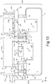
- Figure 13 shows a further embodiment of the protective cap, according to a further aspect of the present invention.
- the cap is not obtained via machining of a wafer 400 of semiconductor material, but using a wafer 500 of material transparent to the light radiation that, in use, impinges upon the reflecting layer of the micromirror 104 (for example, glass).
- the wafer 500 is machined with techniques in themselves known in a way similar to what is illustrated in Figures 10A and 10B for the wafer 400 to form a covering region 124' for the TMOS transistor 26 similar to the covering region 124 described previously and having similar functions. However, in this case, through openings are formed passing through the wafer 500 only at the regions which (when the wafer 500 and the stack 250 are coupled together) are aligned, along the axis Z, with the metal contacts 74, 75, 76, and 77.
- Coupling between the wafer 500 and the stack 250 is obtained by means of the flip-chip process, to obtain the stack 550 of Figure 14.
- the getter is absent.
- a covering region 125 (e.g., as has been said, made of glass) is instead present, which extends over the reflecting layer of the micromirror 104.
- the wafer 500 is coupled to the wafer 200 by means of coupling regions 112-114 similar to the ones described with reference to Figures 10A-11 and consequently designated by the same reference numbers.
- the micromirror covering region 125 enables protection of the micromirror 104 and at the same time allows penetration of the light radiation that comes from outside and impinges, in use, upon the reflecting layer of the mobile mass.
- both the chamber of the micromirror 141 and the chamber of the TMOS transistor 140 are in a low-pressure condition (PI).
- integration of a micromirror and of a TMOS transistor in one and the same wafer enables reduction of the area necessary for manufacturing the system comprising the TMOS transistor and the micromirror, and hence makes it possible to obtain a device that is small and easy to handle.
- the measurement using the TMOS transistor is more accurate than what is currently available in the prior art, and this is due to the possibility of controlling the radiation incident on the body to be heated via the micromirror, in an efficient and precise way.
- TMOS transistor integrated with a micromirror facilitates identification of known illnesses and disorders, with consequent positive effects for the purposes of preventive medicine.
- the above integrated component can moreover be readily generalized to make up for multiple needs, not exclusively in the diagnostic field.
- These variants may be obtained by adjusting the parameters of the TMOS transistor as a function of the frequency in the infrared that is to be measured and that depends upon the application itself.
- an alternative embodiment comprises an integrated component 1 in which the covering region 124 is absent. Consequently, the TMOS transistor 26 is not insulated fluidically and thermally from the external environment. Noise in the measurement of the electromagnetic radiation R3 by the TMOS transistor 26, due, for example, to thermal fluctuations of the external environment, may be eliminated by carrying out this measurement in a differential mode with the aid, for example, of a temperature sensor integrated in the component 1, or otherwise coupled to the component 1, or arranged in the proximity of the component 1.
- This temperature sensor is adapted to record the temperature of the external environment and to supply at output an electrical signal proportional thereto: the effect of the thermal fluctuations of the external environment can thus be subtracted from the electrical signal coming out of the TMOS transistor 26, enabling a high degree of accuracy of measurement even in the absence of the covering region 124 and of the air-tight chamber 140.
Landscapes
- Physics & Mathematics (AREA)
- General Physics & Mathematics (AREA)
- Optics & Photonics (AREA)
- Engineering & Computer Science (AREA)
- Manufacturing & Machinery (AREA)
- Microelectronics & Electronic Packaging (AREA)
- Chemical & Material Sciences (AREA)
- Crystallography & Structural Chemistry (AREA)
- Micromachines (AREA)
- Apparatuses And Processes For Manufacturing Resistors (AREA)
- Electrical Discharge Machining, Electrochemical Machining, And Combined Machining (AREA)
Abstract
Description
- The present invention relates to a method of manufacturing an integrated component, and to the integrated component. In particular, the present invention relates to a method of manufacturing a component comprising a micromirror and a thermal MOS (TMOS) transistor, in particular adapted to be used in a system for 3D reconstruction of a body irradiated with radiation in the near infrared (NIR).
- Medical examinations of a known type envisage generation of 3D images obtained starting from a body irradiated with NIR radiation, enabling reconstruction of the thermal spectrum of the body itself and consequently identification of potential illnesses or disorders, such as rheumatoid arthritis, Raynaud's syndrome, osteoarthritis of the knee, etc. Various systems are known for carrying out such medical examinations, which require both a light source in the NIR spectrum, for irradiating via incident radiation the portion of body of the patient under examination, and a detector adapted to measure the radiation coming out of the portion of irradiated body. Wide and poorly localised beams of incident radiation are thus generated, with consequent reduction of precision and accuracy of the signal that is emitted by the body under examination and is acquired by the detector.
- Detectors of a known type envisage use of a TMOS transistor. The TMOS transistor is a field-effect transistor device typically used in sensor applications for determining the amount of radiation emitted by an object or body under examination. The radiation emitted, received by the TMOS transistor, causes generation of charge carriers at the conductive channel of the TMOS transistor and, hence, a variation of the output current; the latter can be set in relation with the amount of radiation emitted by the object under examination.
- It is moreover known to use a mirror of micrometric dimensions (micromirror MEMS) in order to deflect and direct the radiation that is to impinge upon the body under examination towards a specific region of the body. Generally, the micromirror is obtained by depositing a metal, such as gold or aluminium, on a mobile mass of a die, in order to create a reflecting surface (e.g., so as to achieve a reflectivity higher than 98%). Actuation of the mobile mass of the micromirror is typically of a piezoelectric, capacitive, or magnetic type.
- In particular, actuation of a capacitive type is made possible via electric currents that are supplied to a stator and to a rotor of the micromirror. Such electric currents generate a difference of capacitance across the mobile mass of the micromirror so that said mass, subjected to a twisting moment, can be controlled. The micromirror is typically driven at the resonance frequency of the mobile mass.
- Systems of a known type present various disadvantages. In particular, systems of a known type are constituted by numerous components physically separated from one another. This leads to an increase in the dimensions of the system as a whole and a difficulty in obtaining a synergistic operation of the components of said system (e.g., there exists an effective difficulty in orienting the radiation on a specific point of the body to be analysed and detecting the radiation emitted by the body with a high degree of precision).
- The aim of the present invention is to provide a method of manufacturing an integrated component, and a corresponding integrated component that will overcome the limits of the prior art.
- According to the present invention, a method of manufacturing an integrated component, and an integrated component are provided, as defined in the annexed claims.
- For a better understanding of the present invention, a preferred embodiment thereof is now described, purely by way of non-limiting example, with reference to the attached drawings, wherein:
-
Figures 1-11 show, in a side cross-section view, steps for manufacturing an integrated component according to an embodiment of the present invention; -
Figure 12 is a schematic illustration of a system that includes the integrated component manufactured according to the steps ofFigures 1-11 ; and -
Figure 13 shows an integrated component according to a further embodiment of the present invention. -
Figures 1-11 illustrate, in a side cross-section view, in a triaxial cartesian reference system X, Y, Z, steps of manufacturing an integrated component 1 illustrated as a whole inFigure 11 . The integrated component 1 comprises a detector device, in particular a TMOS transistor, and a micromirror, in particular obtained via MEMS technology, as illustrated more fully in what follows. - With reference to
Figure 1 , afirst wafer 100 is arranged, including asubstrate 2, made of semiconductor material such as silicon, which includes atop surface 2a opposite, along Z, to abottom surface 2b. The thickness of thesubstrate 2, measured along Z, between thetop surface 2a and thebottom surface 2b ranges, for example, between 300 µm and 600 µm. Aninsulating layer 9, here made of silicon oxide (thermal oxide), surrounds thesubstrate 2 and has, by way of example, a thickness of approximately 1 µm. - Once again with reference to
Figure 1 , theinsulating layer 9 is shaped by means of lithographic and etching steps in themselves known in order to remove selective portions thereof at thetop surface 2a. More in particular, theinsulating layer 9 is removed from regions of thetop surface 2a where at least two bonding rings are to be formed, where a first bonding ring is identified by the reference number 4 (withsections sections insulating layer 9 is likewise removed from regions of thetop surface 2a where at least onebonding pad 3 and at least onemetal contact 8 are to be formed. Theinsulating layer 9 is likewise removed from regions of thetop surface 2a where trenches will be formed useful for operation of the TMOS transistor and of the micromirror, in particular in portions of thetop surface 2a internally delimited by thebonding rings - A step of masked implantation is then carried out, in a way in itself known, to form, in a position corresponding to the
top surface 2a, an implantedregion 10, in particular of an N type. The implantedregion 10 extends in a portion of thetop surface 2a ranging between thebonding ring 4 and thebonding ring 5. - Formation of the
bonding rings bonding pad 3, and of themetal contact 8 is obtained, in one embodiment, simultaneously, and includes a step of deposition of a metal layer on thetop surface 2a of thesubstrate 2, in particular germanium deposited, for example by sputtering, and a subsequent step of photolithographic and etching definition of said deposited metal layer. The photolithographic step and the subsequent etching step are carried out using an appropriate mask, configured to define the desired shape and extension of thebonding rings bonding pad 3, and of the metal contact 8 (according to the design specifications). - The
bonding rings bonding pad 3 are formed in electrical contact with thesubstrate 2. Themetal contact 8 is formed at, and in electrical contact with, thedoped region 10. Thisdoped region 10 provides an electrical connection between themetal contact 8 and thesubstrate 2; themetal contact 8 has, in use, the function of earth reference terminal. - With reference to
Figure 2 , a step of etching of thefirst wafer 100 is carried out to form a first trench 16 (useful for operation of the micromirror). For this purpose, afirst mask 15 is used, which has a first opening 15a; thefirst mask 15 is such that, when used, it covers thetop surface 2a of thesubstrate 2 except for a surface region of the latter that is designed to house the first trench 16 (i.e., at the first opening 15a). More in particular, thefirst trench 16 is formed inside thesecond bonding ring 5, i.e., in a cross-section view, between thesections second bonding ring 5. A dry-etching step, represented byarrows 17, enables removal of portions of thesubstrate 2 not protected by thefirst mask 15. Dry etching proceeds to a depth z1, measured along the direction Z starting from thetop surface 2a, of some tens of micrometres, for example 60 µm. According to one embodiment, thefirst trench 16 is provided by means of deep reactive ion etching (DRIE). - Then (
Figure 3 ), asecond trench 21 is formed (useful for operation of the TMOS transistor), and formation of thefirst trench 16 is likewise completed, using asecond etching mask 20. In particular, thesecond mask 20 has a first opening similar to the first opening 15a already present in the first mask 15 (and for this reason identified by the same reference number) and a second opening 20a at the surface region where thesecond trench 21 is to be formed. More in particular, thesecond trench 21 is formed inside the first bonding ring 4 (i.e., in a cross-section view, between thesections - By carrying out a dry etch (identified by the arrows 22), in particular of the same type as the etch represented in
Figure 2 , thesubstrate 2 is selectively removed to form thesecond trench 21, and etching of thefirst trench 16 is continued. The etch represented inFigure 3 proceeds until a depth of thefirst trench 16 is reached equal to approximately 160 µm along the axis Z, and a depth z2 of thesecond trench 21 is reached equal to approximately 100 µm (measured along the axis Z, starting from thetop surface 2a) . - The
first trench 16 and thesecond trench 21 are set apart from each other, along the direction of the axis X in a cross-section view, by a distance x1 equal to some hundreds of micrometres (for example, 100-200 µm). - A further etching step (e.g., via RIE), using the
first mask 15 ofFigure 2 (or a similar mask, which has the opening 15a at the trench 16), is carried out so as to generate, in a way in itself known, blackening of thefirst trench 16 in order to obtain black silicon. Black silicon has a high absorption coefficient of radiation, typically greater than 95%, in particular equal to, or higher than, 99% and is used for reducing, in use, an undesired reflection of light radiation from thefirst trench 16 towards the micromirror. - Other methods for reducing the reflectivity of the
first trench 16 may be implemented, in a way in itself known to the person skilled in the art, for example, via deposition of non-reflecting material (e.g., carbon black, or other organic materials adapted for the purpose). - Alternatively, the step of blackening of the first trench can be carried out using the
second mask 20 ofFigure 3 ; in this case, the process of blackening of the silicon causes, in addition to blackening of thefirst trench 16, also blackening of thesecond trench 21. In this embodiment, there is the advantage of speeding up the manufacturing steps in so far as thesecond mask 20 already present after the etching steps ofFigure 3 is exploited. - With reference to
Figure 4 , a secondpre-machined wafer 200 is now illustrated. Thewafer 200 is shown in a side cross-section view, in the same triaxial reference system X, Y, Z as that ofFigure 1 . - The
second wafer 200 is manufactured using CMOS technology via processes and techniques in themselves known that do not form part of the present invention. - The
second wafer 200 comprises asubstrate 28 of semiconductor material (having a thickness ranging between 500 µm and 900 µm, preferably 750 µm), such as silicon, extending over which is astructural body 32. Thestructural body 32 has afirst surface 32a and asecond surface 32b, extending between which is a region 29 (e.g., including one or more layers of epitaxial silicon, dielectric layers, and metal layers) and aninsulating layer 33 interposed between theregion 29 and thesubstrate 28. Theinsulating layer 33 has the function of electrical insulator towards thesubstrate 28. - The
second wafer 200 comprises a third bonding ring 40 (sections Figure 4 ) and a fourth bonding ring 42 (sections Figure 4 ). Both thethird bonding ring 40 and thefourth bonding ring 42 are made of metal material chosen so that it will form a eutectic alloy with the metal material used to form the first and thesecond bonding rings wafer 100. In one embodiment, the metal material of the first and thesecond bonding rings fourth bonding rings - In particular, when coupled together, the
fourth bonding ring 42 and thefirst bonding ring 4 form a bond that guarantees an air-tight seal; i.e., it prevents passage of gas molecules (e.g., air) through it. The same applies to the coupling between thethird bonding ring 40 and thesecond bonding ring 5. - According to one aspect of the present invention, the
region 29 houses aTMOS transistor 26, integrated in theregion 29 and set facing thefirst surface 32a of thestructural body 32. TheTMOS transistor 26 extends inside thefourth bonding ring 42. TheTMOS transistor 26 is electrically coupled to a conductive pad 38 (made, for example, of germanium), which extends on thefirst surface 32a of thestructural body 32, on the outside of thefourth bonding ring 42. - One or more conductive through
vias 35, in electrical contact with theconductive pad 38, extend completely through theregion 29 and the insulatinglayer 33, until they reach and contact thesubstrate 28. The one or more conductive throughvias 35 are electrically insulated from theregion 29. Theconductive pad 38 is likewise in electrical connection with theTMOS transistor 26 and has the function of receiving the output signal of theTMOS transistor 26. For this purpose, thesubstrate 28 is of a doped type (e.g., of an N type), or has doped regions (e.g., of an N type), or conductive paths (e.g., metal paths) for conveying the signal of the TMOS transistor towards conductive pads, where said signal is acquired. - The
conductive pad 38 is electrically insulated from theregion 29 by abottom dielectric layer 34, which extends between theconductive pad 38 and theregion 29 except for the portion where the conductive throughvias 35 are present, and is insulated, at the side, by means of aside dielectric layer 36. Thedielectric layer 36 exposes a top portion of theconductive pad 38, to enable top electrical contact thereof, as illustrated more fully hereinafter. - A
metal contact 44, having the function of earth reference contact, extends on thefirst surface 32a of thestructural body 32 between thethird bonding ring 40 and thefourth bonding ring 42. - A conductive through via 46 extends through the
region 29 at themetal contact 44, electrically connecting themetal contact 44 to thesubstrate 28. - With reference to
Figure 5 , thefirst surface 32a of thestructural body 32 is coated by a layer ofpassivating material 50 such as silicon nitride (Si3N4), for example, having a thickness of between 1-3 µm. - The
passivating layer 50 is shaped by means of lithographic and etching steps, using athird mask 52 and selectively etching thepassivating layer 50. In particular, thethird mask 52 covers and protects from etching the portions of thepassivating layer 50 that extend in areas corresponding to theTMOS transistor 26, thethird bonding ring 40, thefourth bonding ring 42, themetal contact 44, theconductive pad 38, and thedielectric layer 36 that insulates theconductive pad 38 at the side. - Then (
Figure 6 ), a second etch is carried out, such as a dry etch or DRIE, to remove selective portions of thestructural body 32 in areas corresponding to the exposed regions (i.e., no longer covered by the passivating layer 50). In this step, thepassivating layer 50 functions as etching mask, to protect the surface regions of thewafer 200 covered by thepassivating layer 50. Removal of the selective portions of thestructural body 32 proceeds until thesubstrate 28 is reached. - Next, the
passivating layer 50 is completely removed from thewafer 200. The portions of thewafer 200 that were covered by thethird mask 52 during theetching step 51 ofFigure 5 are thus exposed. - Once again with reference to
Figure 6 , thethird bonding ring 40 delimits, at the top, afirst ring region 60, which is formed by a portion of thestructural body 32 not previously removed and extends underneath thethird bonding ring 40. Thefourth bonding ring 42 delimits, at the top, asecond ring region 62, which is formed by a respective portion of thestructural body 32 not previously removed and extends underneath thefourth bonding ring 42. Aregion 64 completely houses theTMOS transistor 26, whereas aregion 66 completely houses the conductive throughvias 35 and theconductive pad 38, and is covered on the surface by thedielectric layer 36. Aregion 68 is moreover formed, which is delimited, at the top, by themetal contact 44 and houses the conductive through via 46. - With reference to
Figure 7 , thewafer 200 ofFigure 6 is flipped over through 180° and set in contact with thewafer 100 ofFigure 3 , according to the method known as "flip-chip". - In particular, this method is carried out so as to set in electrical contact: the
bonding pad 3 with theconductive pad 38; themetal contact 44 with themetal contact 8; thefirst bonding ring 4 with thefourth bonding ring 42; and thesecond bonding ring 5 with thethird bonding ring 40. - A
stack 250 is thus obtained, formed by thewafer 200 set on top of thewafer 100, along Z. - The electrical contacts thus formed are then heated, for example, by means of a step of heating to a temperature ranging between 200°C and 400°C of the
stack 250, in order to create a eutectic alloy between the metal of theelements respective elements - The contact between the
first bonding ring 4 and thefourth bonding ring 42 defines afirst chamber 70 that is in adapted to house theTMOS transistor 26, which thus faces thesecond trench 21. - The contact between the
second bonding ring 5 and thethird bonding ring 40 defines asecond chamber 72, which is adapted to house the micromirror, which will thus face thefirst trench 16. - The
substrate 28 has afirst surface 80a and asecond surface 80b, opposite to each other along the axis Z. Thesecond surface 80b of the substrate 28 (belonging to the wafer 200) faces thefirst surface 2a of the substrate 2 (belonging to the wafer 100). Thefirst surface 80a of thesubstrate 28 is, instead, exposed towards an external environment. - This is followed by lapping of the
first surface 80a of thesubstrate 28, with reduction, if necessary, of the thickness thereof along the axis Z until a final thickness of some tens of micrometres and, for example, of approximately 65 µm is reached. - Then, on the
first surface 80a of thesubstrate 28, with known deposition, lithographic, and etching techniques, metal contacts 74-77 are formed. The metal contacts 74-77 are, for example, made of aluminium, titanium, or gold, or a titanium-gold alloy. In particular, themetal contact 74 is formed vertically aligned (i.e., along Z) with theconductive pad 38, themetal contact 75 is vertically aligned to themetal contact 44, themetal contact 76 is, according to a non-limiting embodiment, vertically aligned with thesection 40a of thethird bonding ring 40, and themetal contact 77 is, according to a non-limiting embodiment, vertically aligned with thesection 40b of thethird bonding ring 40. More in general, and in a way that does not imply any limitation of the present invention, themetal contacts bonding ring 5 and of thebonding ring 40. - The
metal contacts vias substrate 28 and previously obtained for said purpose, whereas themetal contacts - In this way, the
metal contact 74 forms a pad for supply of the current signal coming from theTMOS transistor 26. - The through via 35 connects the TMOS transistor to the
metal contact 74 and passes inside the dielectric layers of the stack formed so far. Thecontact 38, which is typically used for wire bonding to read the output signal is, in this context, used as further bonding layer. Given that theTMOS transistor 26 is flipped over on account of the flip-chip operation described previously, the via 35 carries the signal to themetal contact 74 through the silicon, to enable, for example, via wire bonding, reading of the signal of theTMOS transistor 26 supplied at themetal contact 74. Themetal contact 75 is adapted to function as an earth contact for the micromirror. Themetal contact 76 and themetal contact 77 supply the driving currents to the rotor and to the stator of the micromirror, as illustrated more fully hereinafter. - In particular, with reference to
Figure 8 , further lithographic and etching steps (not illustrated in detail) are carried out, for shaping thesubstrate 28 at thesurface 80a. - In particular, the
substrate 28 is etched to form a plurality of functional regions. - A
first region 90 of thesubstrate 28 is delimited, at the top, by themetal contact 74, and asecond region 91 is delimited, at the top, by themetal contact 75. The first and thesecond regions TMOS transistor 26 and for providing an earth reference signal, respectively. - A
third region 92 of thesubstrate 28 houses theTMOS transistor 26. - A
fourth region 93 of thesubstrate 28 forms a portion of the micromirror, in particular the mobile mass that carries the reflecting element, suspended over thecavity 72 and over thefirst trench 16 by means of torsion springs of a type in itself known. - A
fifth region 94 of thesubstrate 28 carries, at the top, themetal contact 76 and forms the rotor of the micromirror. Asixth region 95 of thesubstrate 28 carries, at the top, themetal contact 77 and forms the stator of the micromirror. Both the fifth region 94 (rotor) and the sixth region 95 (stator) are capacitively coupled to the fourth region 93 (mobile mass) in a way in itself known and such that, when appropriately biased, generate an oscillation of the mobile mass of the micromirror. The stator and rotor of the micromirror are biased, in use, via therespective metal contacts - Moreover, a
seventh region 96 extends so as to correspond vertically with thesection 42b of thefourth bonding ring 42. Aneighth region 97 and aninth region 98 extend laterally alongside thefirst region 90. - It may be noted that the regions 90-97 mentioned previously are electrically insulated from one another.
- With reference to
Figure 9 , a third wafer 300 (e.g., having a thickness ranging between 300 µm and 700 µm, preferably 400 µm) is coupled to thestack 250, in particular on thesecond wafer 200. - In particular, two or more coupling (or bonding)
elements third wafer 300 to thesecond wafer 200. In particular, thecoupling elements metal contacts coupling element 101a is coupled to theeighth region 97, whereas acoupling element 101b is coupled to thesixth region 95. - The
coupling elements third wafer 300 and to avoid contact of thethird wafer 300 with the second wafer 200 (except, of course, for the coupling points between the twowafers 200, 300). - The
coupling elements wafers - The
third wafer 300 has the function of mask for enabling protection and handling of thestack 250, and may be made of semiconductor material, such as silicon. Thewafer 300 is subjected to lithographic and etching steps to form anopening 310 at themobile mass 93 of the micromirror. Theopening 310 may be formed prior to the step of coupling between thewafer 300 and thestack 250, or else subsequently, according to respective modalities evident to the person skilled in the art. - A step of deposition of reflecting material, for example metal material, (step designated by
arrows 105 inFigure 9 ) is carried out, for example, via the sputtering technique. This step ofmetal deposition 105 enables creation of ametal layer 103 on the areas not covered by thethird wafer 300, i.e., on the fourth region 93 (mobile mass of the micromirror) . Themetal layer 103 may be constituted by a highly reflecting metal (for example, with a reflection coefficient higher than 95% - typically between 95% and 98%), such as aluminium or gold, or AlCu. Manufacturing of the micromirror (designated by thereference 104 inFigure 9 ) is thus completed. - Once metal deposition is finished, both the
third wafer 300 and thecoupling elements - This is followed by steps of manufacturing a protective cap for the
stack 250 thus obtained. - An embodiment of the protective cap is described in what follows, with reference to
Figures 10A-11 . - With reference to
Figure 10A , afourth wafer 400 is processed to create the protective cap. In particular, thefourth wafer 400 comprises asubstrate 111 of semiconductor material, such as silicon, having afirst surface 111a and asecond surface 111b. The thickness of thesubstrate 111, between thefirst surface 111a and the second 111b surface (i.e., along the axis Z), ranges between approximately 300 µm and 800 µm, for example, 400 µm. Thesubstrate 111 may be of a pre-processed type and may include, for example, one or more epitaxial layers. - In a machining step, the
fourth wafer 400 is subjected to lithographic and etching steps to remove selective portions of thesubstrate 111 in order to form arecess 111a' at thefirst surface 111a. Therecess 111a' is formed in a region of thewafer 400 that, in subsequent manufacturing steps (Figure 11 ) will be orientated facing thestack 250, in particular facing theTMOS transistor 26. - The
recess 111a' has a depth, along the axis Z starting from thefirst surface 111a, equal to, for example, approximately 5 µm, and a width, along the axis X, equal to, for example, approximately 50 µm. In top plan view in the plane XY, the recess has a quadrangular shape, for example square, or else a circular or generically polygonal shape. Therecess 111a' is configured to house a gas-absorbing material, known as "getter", which is designated inFigure 10A by thereference 110. - The
getter 110 is usually made of material deposited in the form of a layer, and has the function of absorbing specific gas molecules. Materials used as getter layer are known, and comprise, for example, metals such as aluminium (Al), barium (Ba), zirconium (Zr), titanium (Ti), vanadium (V), iron (Fe), or mixtures or alloys thereof, such as zirconium-aluminium, zirconium-vanadium-iron, zirconium-nickel, zirconium-cobalt (in particular, an alloy of Zr/Co/O). The getter material may be deposited in therecess 111a' by means of a lift-off process. In this case, the same photoresist used for photolithographic definition of therecess 111a' is kept on thewafer 400 also during the step of deposition of the getter material. A subsequent lift-off step enables removal of the photoresist from thewafer 400 and retention of the getter material only inside therecess 111a', in a self-aligned way. - Moreover, a plurality of coupling regions is formed, in particular glassfrit regions, 112-114, the section views of which (112a, 112b; 113a, 113b; 114a, 114b) are illustrated in
Figure 11A . Each coupling region has a thickness, along the axis Z, equal to, for example, approximately 5 µm and a width, in a section view along the axis X, equal to, for example, approximately 10 µm. - The
coupling region 112 is, in top plan view in the plane XY, a ring that internally encloses thecoupling regions getter 110. In a different embodiment, thecoupling region 112 is not a ring, and is instead formed by a plurality of regions physically separated from one another. - The
coupling region 113 is, in top plan view in the plane XY, a ring having a diameter greater than the distance, along X, between the stator and the rotor of themicromirror 104 so that, when thewafer 400 is coupled to the stack 250 (Figure 11 ), thecoupling region 113 extends outside the stator and rotor regions (or in positions corresponding thereto), completely surrounding themicromirror 104. - It is evident that the
coupling region 113 may not be a ring and may be, instead, formed by a plurality of regions physically separated from one another and such as to surround themicromirror 104 only partially. In fact, themicromirror 104 does not need to be located in a closed or air-tight chamber. - The
coupling region 114 is, in top plan view in the plane XY, a ring that internally encloses thegetter 110. When thewafer 400 is coupled to the stack 250 (Figure 11 ), thecoupling region 114 forms an air-tight coupling, insulating an internal environment, including the getter, from an external environment, as illustrated more fully in what follows. For this purpose, thecoupling region 114 completely surrounds thegetter 110 and may in any case have a shape different from the circular one, for example, oval or polygonal. - The structure of
Figure 10A then undergoes (Figure 10B ) a lithographic and etching process, for example, a RIE or DRIE process, for removing selective portions of thefourth wafer 400, throughout its thickness. - In particular, according to the present invention, the
fourth wafer 400 is etched so as to remove regions of thewafer 400 not protected at the top by the coupling regions 112-114. Thewafer 400 is moreover not etched at the internal surface delimited by the coupling region 114 (where thegetter 110 is present). A plurality of structural support regions 120-123, and acovering region 124 is thus formed. - A first through
opening 131 which extends in a position corresponding to therotor contact 76, between thestructural support region 122 and thecovering region 124, and is shaped so as to form an access for providing electrical contact (for example, by means of wire bonding) with therotor contact 76. A second through opening 133 which extends in a position corresponding to thestator contact 77, between thestructural support region 120 and thestructural support region 121 and is shaped so as to form an access for providing electrical contact (for example, by means of wire bonding) with thestator contact 77. A third through opening 134 which extends in a position corresponding to themicromirror 104, between thestructural support region 121 and thestructural support region 122, and is shaped so as to form an optical access for the radiation incident on and coming out of the reflectinglayer 103 of themicromirror 104. A fourth through opening 135 which extends in a position corresponding to themetal contact 74, between thestructural support region 123 and thecovering region 124, and is shaped so as to form an access for providing electrical contact (for example, by means of wire bonding) with themetal contact 74. - As illustrated in reference to
Figure 11 , the structure ofFigure 10B is set in contact with thestack 250 ofFigure 10 (with the flip-chip method). - In particular, the
coupling region 112, which is more external, is set in contact with theeighth region 97 and with thesixth region 95 of thesecond wafer 200; thecoupling region 114 is set in contact with theninth region 98 and with theseventh region 96; thecoupling region 113 is set in contact with thefifth region 94 and with thesixth region 95. - In greater detail, the
coupling region 112 extends outside themetal contacts wafer 400; thecoupling region 114 completely surrounds, in top plan view in the plane XY, theTMOS transistor 26, to form an air-tight chamber 140, fluidically insulated from the environment external to saidchamber 140; thecoupling region 113 surrounds (at least partially, as described previously) the mobile mass of themicromirror 104, exposing the reflecting layer of themicromirror 104, which is thus accessible from outside for a light beam incident thereon. Also themetal contacts wafer 400. - After coupling between the
wafer 400 and thestack 250, the structure thus formed (stack 450) is heated to a high temperature (for example 350-450°C) to bring about melting of the glassfrit of the coupling regions 112-114 and achieve a permanent bonding of thewafer 400 to thewafer 200. - This is followed by activation of the
getter 110 to generate a pressure P1, inside thechamber 140 that houses the TMOS transistor, lower than the pressure P2 outside thechamber 140. For instance, the pressure P1 ranges between 10-2 and 10-3 mbar. - The micromirror 104 (in particular, the mobile mass) is actuated capacitively, by appropriately biasing (in a way that is in itself known and does not form the subject of the present invention) the rotor (i.e., the
fifth region 94 enabling biasing via the metal contact 76) and the stator (enabling biasing via the metal contact 77). Said biasing causes an unbalancing of the mobile mass, which is driven in oscillation, in particular at its resonance frequency. - With joint reference to
Figures 11 and12 , during use, themicromirror 104 receives light radiation R1 on the reflecting layer through the corresponding opening in thewafer 400, and directs reflected light radiation R2 towards a point in space or a body 150 (for example, a region of the body of a patient). - Incidence of said light radiation R2 on the
body 150 causes an increase in the temperature thereof, and a consequent emission of radiation R3 by saidbody 150, with an intensity that depends upon the temperature of thebody 150 itself. - Since the
TMOS transistor 26 is sensitive to electromagnetic radiation R3 emitted by thebody 150, the rise in temperature of the latter is detected by theTMOS transistor 26 and transduced into a current signal at output from theTMOS transistor 26. The vacuum present in thechamber 140 that houses theTMOS transistor 26 thermally decouples thechamber 140 from the external environment, and enables an increase in the accuracy of the measurement. - Even though the electromagnetic radiation R3 emitted by the
heated body 150 impinges upon the back of theTMOS transistor 26, this does not create problems of measurement since the measurement of temperature is independent of the direction of incidence of the electromagnetic radiation on theTMOS transistor 26. - It is moreover known that a warm body emits electromagnetic radiation in the infrared, and that this electromagnetic radiation is not absorbed and blocked to a significant extent by a layer of semiconductor material having a thickness of some hundreds of micrometres, such as the
region 124 of thewafer 400 that covers thechamber 140. Consequently, thecovering region 124 does not prevent the electromagnetic radiation from reaching theTMOS transistor 26 so that it can be detected. - It is, instead, expedient for the region above the
micromirror 104 not to be covered by a layer of material such as to block the light radiation incident upon the reflecting layer. - The electrical signal generated at output from the
TMOS transistor 26 is acquired via themetal contact 74, to be subsequently processed. -
Figure 13 shows a further embodiment of the protective cap, according to a further aspect of the present invention. - In this case, the cap is not obtained via machining of a
wafer 400 of semiconductor material, but using awafer 500 of material transparent to the light radiation that, in use, impinges upon the reflecting layer of the micromirror 104 (for example, glass). - The
wafer 500 is machined with techniques in themselves known in a way similar to what is illustrated inFigures 10A and 10B for thewafer 400 to form a covering region 124' for theTMOS transistor 26 similar to thecovering region 124 described previously and having similar functions. However, in this case, through openings are formed passing through thewafer 500 only at the regions which (when thewafer 500 and thestack 250 are coupled together) are aligned, along the axis Z, with themetal contacts - Coupling between the
wafer 500 and thestack 250 is obtained by means of the flip-chip process, to obtain thestack 550 of Figure 14. - In the embodiment of
Figure 13 , the getter is absent. - A covering region 125 (e.g., as has been said, made of glass) is instead present, which extends over the reflecting layer of the
micromirror 104. - The
wafer 500 is coupled to thewafer 200 by means of coupling regions 112-114 similar to the ones described with reference toFigures 10A-11 and consequently designated by the same reference numbers. - To obtain the pressure P1 (which is lower than P2) inside the
chamber 140 that houses theTMOS transistor 26, coupling between thewafer 500 and thestack 250 is made in an environment at the pressure P1. - The
micromirror covering region 125 enables protection of themicromirror 104 and at the same time allows penetration of the light radiation that comes from outside and impinges, in use, upon the reflecting layer of the mobile mass. - In this embodiment, both the chamber of the
micromirror 141 and the chamber of theTMOS transistor 140 are in a low-pressure condition (PI). - From an examination of the characteristics of the invention provided according to the present disclosure, the advantages that it affords are evident.
- In particular, integration of a micromirror and of a TMOS transistor in one and the same wafer enables reduction of the area necessary for manufacturing the system comprising the TMOS transistor and the micromirror, and hence makes it possible to obtain a device that is small and easy to handle.
- The measurement using the TMOS transistor is more accurate than what is currently available in the prior art, and this is due to the possibility of controlling the radiation incident on the body to be heated via the micromirror, in an efficient and precise way.
- Use of a compact and integrated system enables reduction of the time necessary to obtain the result of the measurement, and moreover enables use thereof at room temperature.
- Use of a TMOS transistor integrated with a micromirror facilitates identification of known illnesses and disorders, with consequent positive effects for the purposes of preventive medicine.
- The above integrated component can moreover be readily generalized to make up for multiple needs, not exclusively in the diagnostic field. These variants may be obtained by adjusting the parameters of the TMOS transistor as a function of the frequency in the infrared that is to be measured and that depends upon the application itself.
- Finally, it is clear that modifications and variations may be made to the invention described and illustrated herein, without thereby departing from the scope thereof, as defined in the annexed claims.
- In particular, an alternative embodiment comprises an integrated component 1 in which the
covering region 124 is absent. Consequently, theTMOS transistor 26 is not insulated fluidically and thermally from the external environment. Noise in the measurement of the electromagnetic radiation R3 by theTMOS transistor 26, due, for example, to thermal fluctuations of the external environment, may be eliminated by carrying out this measurement in a differential mode with the aid, for example, of a temperature sensor integrated in the component 1, or otherwise coupled to the component 1, or arranged in the proximity of the component 1. This temperature sensor is adapted to record the temperature of the external environment and to supply at output an electrical signal proportional thereto: the effect of the thermal fluctuations of the external environment can thus be subtracted from the electrical signal coming out of theTMOS transistor 26, enabling a high degree of accuracy of measurement even in the absence of thecovering region 124 and of the air-tight chamber 140.
Claims (18)
- A method of manufacturing an integrated component (1), comprising the steps of:- providing a first wafer (100) of semiconductor material, having a surface (2a);- providing a second wafer (200) of semiconductor material, including a substrate (28) and a structural layer (32) on the substrate (28), the structural layer (32) integrating a detector device (26) for detecting electromagnetic radiation (R3);- coupling the structural layer (32) of the second wafer (200) to the surface (2a) of the first wafer (100); and- processing the substrate (28) of the second wafer (200) to form a stator (95), a rotor (94), and a mobile mass (93) of a micromirror (104), said stator (95) and rotor (94) forming a capacitive-driving assembly for capacitively driving the mobile mass (93).
- The method according to Claim 1, further comprising the step of coupling a first cap (124) to the substrate (28) in correspondence of the detector device (26),
and wherein the steps of coupling the structural layer (32) to the surface (2a) and coupling the cap (124) to the substrate (28) are carried out so as to form a first air-tight chamber (140) that houses said detector device (26). - The method according to Claim 2, further comprising the steps of:forming a stator contact (77), electrically coupled to the stator (95) of the micromirror (104); andforming a rotor contact (76), electrically coupled to the rotor (94) of the micromirror (104),wherein coupling the first cap (124) to the substrate (28) includes coupling a third wafer (400) to the substrate (28), and shaping the third wafer (400) so as to form: said first cap (124), a first through opening (131) at the rotor contact (76), and a second through opening (133) at the stator contact (77).
- The method according to Claim 2 or 3, further comprising the step of coupling a second cap (124') to the substrate (28) at the micromirror (104),
and wherein the steps of coupling the structural layer (32) to said surface (2a) and coupling the second cap (124') to the substrate (28) are carried out so as to form a second air-tight chamber (141) that houses said micromirror (104). - The method according to Claim 4 when depending upon Claim 3, wherein coupling the second cap (124') to the substrate (28) includes shaping the third wafer (500) so as to form: said first cap (124), said second cap (124'), the first through opening (131), and the second through opening (133) .
- The method according to Claim 4 or 5, wherein the first cap (124) and the second cap (124') are jointly formed by machining of one and the same wafer (500) of glass.
- The method according to any one of the preceding claims, wherein the step of coupling the structural layer (32) of the second wafer (200) to the surface (2a) of the first wafer (100) includes:forming a first coupling ring (42), made of a first material, on the structural layer (32), to surround the detector device (26);forming a second coupling ring (4), made of a second material, on the surface (2a) of the first wafer (100);placing the first and the second coupling rings in mutual contact; andcarrying out a thermal treatment adapted to create a eutectic bond between the first and the second materials.
- The method according to any one of the Claims 2 to 7, further comprising the step of forming a recess (111a') in the cap (124), which gives out onto the air-tight chamber (140) and is configured to house a getter layer (110).
- The method according to any one of the preceding claims, further comprising the steps of:forming in the first wafer (100), starting from the surface (2a), a first trench (16) and a second trench (21); andprocessing at least the first trench (16) to reduce the reflectivity thereof,wherein the step of coupling the structural layer (32) of the second wafer (200) to the surface (2a) of the first wafer (100) includes arranging the second trench (21) facing the detector device (26),and wherein the step of processing the substrate (28) of the second wafer (200) includes forming the stator (95), the rotor (94), and the mobile mass (93) so that they face the first trench (16).
- An integrated component (1) comprising:- a first wafer (100) of semiconductor material, having a surface (2a); and- a second wafer (200) of semiconductor material, including a substrate (28) and a structural layer (32) on the substrate (28), the structural layer (32) integrating a detector device (26) for detecting electromagnetic radiation (R3),
wherein the structural layer (32) of the second wafer (200) is coupled to the surface (2a) of the first wafer (100),
and wherein a stator (95), a rotor (94), and a mobile mass (93) of a micromirror (104) are integrated in the substrate (28) of the second wafer (200), said stator (95) and rotor (94) forming a capacitive-driving assembly for capacitively driving the mobile mass (93). - The integrated component according to Claim 10, wherein a first cap (124) is moreover coupled to the substrate (28) at the detector device (26),
and wherein the structural layer (32) and the cap (124) are coupled, respectively, to the surface (2a) and to the substrate (28) so as to define a first air-tight chamber (140) that houses said detector device (26). - The integrated component according to Claim 11, further comprising:a stator contact (77), electrically coupled to the stator (95) of the micromirror (104);a rotor contact (76), electrically coupled to the rotor (94) of the micromirror (104); anda third wafer (400), coupled to the substrate (28) and shaped so as to form said first cap (124), a first through opening (131) at the rotor contact (76), and a second through opening (133) at the stator contact (77).
- The integrated component according to Claim 11 or 12, wherein a second cap (124') is moreover coupled to the substrate (28) at the micromirror (104),
and wherein the structural layer (32) and the second cap (124') are coupled, respectively, to the surface (2a) and to the substrate (28) so as to define a second air-tight chamber (141) that houses said micromirror (104). - The integrated component according to Claim 13 when depending upon Claim 12, wherein the third wafer (500) is shaped so as to form said first cap (124), said second cap (124'), the first through opening (131), and the second through opening (133).
- The integrated component according to Claim 13 or 14, wherein the first cap (124) and the second cap (124') are made of glass.
- The integrated component according to any one of the Claims 10 to 15, further comprising:a first coupling ring (42), made of a first material, which extends on the structural layer (32) and surrounds the detector device (26); anda second coupling ring (4), made of a second material, which extends on the surface (2a) of the first wafer (100),wherein the first and the second coupling rings are in mutual contact, and wherein the first and the second materials form a eutectic bond.
- The integrated component according to any one of the Claims 11 to 16, further comprising a recess (111a') in the cap (124), inside the air-tight chamber (140), which is configured to house a getter layer (110).
- The integrated component according to any one of the Claims 10 to 17, further comprising:a first trench (16), which extends in the first wafer (100) starting from the surface (2a), facing the stator (95), the rotor (94), and the mobile mass (93) and has a reduced reflectivity; anda second trench (21), which extends in the first wafer (100), starting from the surface (2a), facing the detector device (26).
Applications Claiming Priority (1)
| Application Number | Priority Date | Filing Date | Title |
|---|---|---|---|
| IT102019000000917A IT201900000917A1 (en) | 2019-01-22 | 2019-01-22 | MANUFACTURING METHOD OF AN INTEGRATED COMPONENT WITH IMPROVED SPACE EMPLOYMENT, AND INTEGRATED COMPONENT |
Publications (2)
| Publication Number | Publication Date |
|---|---|
| EP3689816A1 true EP3689816A1 (en) | 2020-08-05 |
| EP3689816B1 EP3689816B1 (en) | 2023-03-01 |
Family
ID=66049611
Family Applications (1)
| Application Number | Title | Priority Date | Filing Date |
|---|---|---|---|
| EP20153241.3A Active EP3689816B1 (en) | 2019-01-22 | 2020-01-22 | Method of manufacturing an integrated component with improved spatial occupation, and integrated component |
Country Status (4)
| Country | Link |
|---|---|
| US (2) | US11276789B2 (en) |
| EP (1) | EP3689816B1 (en) |
| CN (2) | CN212084950U (en) |
| IT (1) | IT201900000917A1 (en) |
Cited By (1)
| Publication number | Priority date | Publication date | Assignee | Title |
|---|---|---|---|---|
| IT202300004521A1 (en) | 2023-03-10 | 2024-09-10 | St Microelectronics Srl | SENSOR DEVICE FOR DETECTING THE PRESENCE OF A FLAME |
Families Citing this family (5)
| Publication number | Priority date | Publication date | Assignee | Title |
|---|---|---|---|---|
| IT201900000917A1 (en) * | 2019-01-22 | 2020-07-22 | St Microelectronics Srl | MANUFACTURING METHOD OF AN INTEGRATED COMPONENT WITH IMPROVED SPACE EMPLOYMENT, AND INTEGRATED COMPONENT |
| EP4001866A1 (en) * | 2020-11-20 | 2022-05-25 | STMicroelectronics S.r.l. | Radiation sensor with an integrated mechanical optical modulator and related manufacturing process |
| DE102021201151A1 (en) * | 2021-02-08 | 2022-08-11 | Fraunhofer-Gesellschaft zur Förderung der angewandten Forschung eingetragener Verein | MEMS package and method for encapsulating a MEMS structure |
| CN115220217A (en) * | 2022-08-30 | 2022-10-21 | 觉芯电子(无锡)有限公司 | Electromagnetic MEMS micro-mirror and preparation method thereof |
| US20240272004A1 (en) * | 2023-02-10 | 2024-08-15 | Stmicroelectronics International N.V. | Process flow for thin contactless thermal sensors |
Citations (1)
| Publication number | Priority date | Publication date | Assignee | Title |
|---|---|---|---|---|
| EP1151962A1 (en) * | 2000-04-28 | 2001-11-07 | STMicroelectronics S.r.l. | Structure for electrically connecting a first body of semiconductor material overlaid by a second body of semiconductor material, composite structure using the electric connection structure, and manufacturing process thereof |
Family Cites Families (14)
| Publication number | Priority date | Publication date | Assignee | Title |
|---|---|---|---|---|
| US5831266A (en) * | 1996-09-12 | 1998-11-03 | Institut National D'optique | Microbridge structure for emitting or detecting radiations and method for forming such microbridge structure |
| JP2006247815A (en) * | 2005-03-14 | 2006-09-21 | Olympus Corp | Mems system and its manufacturing method |
| CN100449724C (en) * | 2006-02-20 | 2009-01-07 | 中芯国际集成电路制造(上海)有限公司 | A wafer inspection device and wafer inspection method |
| US9036231B2 (en) * | 2010-10-20 | 2015-05-19 | Tiansheng ZHOU | Micro-electro-mechanical systems micromirrors and micromirror arrays |
| ITTO20131014A1 (en) * | 2013-12-12 | 2015-06-13 | St Microelectronics Int Nv | ELECTROSTATICALLY ACTIVATED OSCILLATING STRUCTURE WITH CONTROL OF THE START OSCILLATION PHASE, AND RELATED METHOD OF MANUFACTURE AND PILOT METHOD |
| US9678333B2 (en) * | 2014-05-07 | 2017-06-13 | Stmicroelectronics International N.V. | Scanning micromirror with improved performance and related electronic device |
| US9432020B2 (en) * | 2014-06-25 | 2016-08-30 | Stmicroelectronics S.R.L. | Communication cell for an integrated circuit operating in contact and contactless mode, electronic chip comprising the communication cell, electronic system including the chip, and test apparatus |
| CN205262665U (en) * | 2015-06-22 | 2016-05-25 | 意法半导体股份有限公司 | Pressure sensor |
| ITUA20164673A1 (en) * | 2016-06-27 | 2017-12-27 | St Microelectronics Srl | MEMS DEVICE FORMED BY AT LEAST TWO MULTI-PURPOSED STRUCTURAL LAYERS AND RELATIVE PROCESS OF MANUFACTURE |
| IT201600079455A1 (en) * | 2016-07-28 | 2018-01-28 | St Microelectronics Srl | PROCEDURE FOR MANUFACTURING A MEMS TYPE MICROSPECTOR DEVICE AND ITS DEVICE |
| CN109923372B (en) * | 2016-10-25 | 2021-12-21 | 特里纳米克斯股份有限公司 | Infrared optical detector employing integrated filter |
| EP3447560B1 (en) * | 2017-08-23 | 2021-02-24 | Murata Manufacturing Co., Ltd. | A mems reflector system |
| US10811556B2 (en) * | 2017-12-28 | 2020-10-20 | Todos Technologies Ltd. | Multi layered thermal sensor |
| IT201900000917A1 (en) * | 2019-01-22 | 2020-07-22 | St Microelectronics Srl | MANUFACTURING METHOD OF AN INTEGRATED COMPONENT WITH IMPROVED SPACE EMPLOYMENT, AND INTEGRATED COMPONENT |
-
2019
- 2019-01-22 IT IT102019000000917A patent/IT201900000917A1/en unknown
-
2020
- 2020-01-16 US US16/744,865 patent/US11276789B2/en active Active
- 2020-01-21 CN CN202020139175.1U patent/CN212084950U/en not_active Withdrawn - After Issue
- 2020-01-21 CN CN202010072318.6A patent/CN111463148B/en active Active
- 2020-01-22 EP EP20153241.3A patent/EP3689816B1/en active Active
-
2022
- 2022-02-10 US US17/668,739 patent/US12113140B2/en active Active
Patent Citations (1)
| Publication number | Priority date | Publication date | Assignee | Title |
|---|---|---|---|---|
| EP1151962A1 (en) * | 2000-04-28 | 2001-11-07 | STMicroelectronics S.r.l. | Structure for electrically connecting a first body of semiconductor material overlaid by a second body of semiconductor material, composite structure using the electric connection structure, and manufacturing process thereof |
Cited By (2)
| Publication number | Priority date | Publication date | Assignee | Title |
|---|---|---|---|---|
| IT202300004521A1 (en) | 2023-03-10 | 2024-09-10 | St Microelectronics Srl | SENSOR DEVICE FOR DETECTING THE PRESENCE OF A FLAME |
| EP4428441A1 (en) | 2023-03-10 | 2024-09-11 | STMicroelectronics S.r.l. | Sensor device for flame presence detection |
Also Published As
| Publication number | Publication date |
|---|---|
| CN111463148B (en) | 2025-09-12 |
| IT201900000917A1 (en) | 2020-07-22 |
| CN111463148A (en) | 2020-07-28 |
| US11276789B2 (en) | 2022-03-15 |
| US20220165892A1 (en) | 2022-05-26 |
| EP3689816B1 (en) | 2023-03-01 |
| US20200235251A1 (en) | 2020-07-23 |
| US12113140B2 (en) | 2024-10-08 |
| CN212084950U (en) | 2020-12-04 |
Similar Documents
| Publication | Publication Date | Title |
|---|---|---|
| EP3689816B1 (en) | Method of manufacturing an integrated component with improved spatial occupation, and integrated component | |
| JP5614988B2 (en) | Thermal sensor with thermal insulation layer | |
| JP6487032B2 (en) | Sealed package with stress reduction layer | |
| JP5358446B2 (en) | Die temperature sensor | |
| US6762072B2 (en) | SI wafer-cap wafer bonding method using local laser energy, device produced by the method, and system used in the method | |
| JP5078196B2 (en) | Sensor design and process | |
| US8227285B1 (en) | Method and structure of monolithetically integrated inertial sensor using IC foundry-compatible processes | |
| JP5358445B2 (en) | Thermal sensor with increased sensitivity | |
| EP3729022B1 (en) | An infra-red device | |
| JP2010507083A (en) | Sensor with reference sensing element | |
| JP2019504298A (en) | Thermal infrared sensor array in wafer level package | |
| WO2012087369A1 (en) | Techniques for bonding substrates using an intermediate layer | |
| CN101107500A (en) | Sensor with a sensor element | |
| KR20080073723A (en) | Sensor device and manufacturing method thereof | |
| US5541412A (en) | Two dimensional array infrared ray image pickup device | |
| CN112888980A (en) | Solder protection for hermetic wafer level sealing | |
| KR102826379B1 (en) | Method for producing a thermal infrared sensor array within a vacuum-filled wafer level housing | |
| EP0752159B1 (en) | Semiconductor device provided with a microcomponent having a fixed and a movable electrode | |
| US12066324B2 (en) | Radiation sensor with an integrated mechanical optical modulator and related manufacturing process | |
| HU223540B1 (en) | Method of manufacturing a vibrating structure gyroscope | |
| US20240239648A1 (en) | Mems device having an improved cap and manufacturing process thereof | |
| JP2010243365A (en) | Infrared sensor device manufacturing method | |
| US11915924B2 (en) | Semiconductor device and method for manufacturing the same | |
| CN120467513B (en) | System-level chip for sensing, preparation method thereof, and electronic device | |
| JPH06213708A (en) | Infrared sensor and manufacture thereof |
Legal Events
| Date | Code | Title | Description |
|---|---|---|---|
| PUAI | Public reference made under article 153(3) epc to a published international application that has entered the european phase |
Free format text: ORIGINAL CODE: 0009012 |
|
| STAA | Information on the status of an ep patent application or granted ep patent |
Free format text: STATUS: THE APPLICATION HAS BEEN PUBLISHED |
|
| AK | Designated contracting states |
Kind code of ref document: A1 Designated state(s): AL AT BE BG CH CY CZ DE DK EE ES FI FR GB GR HR HU IE IS IT LI LT LU LV MC MK MT NL NO PL PT RO RS SE SI SK SM TR |
|
| AX | Request for extension of the european patent |
Extension state: BA ME |
|
| STAA | Information on the status of an ep patent application or granted ep patent |
Free format text: STATUS: REQUEST FOR EXAMINATION WAS MADE |
|
| 17P | Request for examination filed |
Effective date: 20201221 |
|
| RBV | Designated contracting states (corrected) |
Designated state(s): AL AT BE BG CH CY CZ DE DK EE ES FI FR GB GR HR HU IE IS IT LI LT LU LV MC MK MT NL NO PL PT RO RS SE SI SK SM TR |
|
| GRAP | Despatch of communication of intention to grant a patent |
Free format text: ORIGINAL CODE: EPIDOSNIGR1 |
|
| STAA | Information on the status of an ep patent application or granted ep patent |
Free format text: STATUS: GRANT OF PATENT IS INTENDED |
|
| INTG | Intention to grant announced |
Effective date: 20220825 |
|
| RIN1 | Information on inventor provided before grant (corrected) |
Inventor name: AZPEITIA URQUIA, MIKEL Inventor name: VISALLI, GIUSEPPE Inventor name: MONTAGNA, LINDA Inventor name: SEGHIZZI, LUCA |
|
| GRAS | Grant fee paid |
Free format text: ORIGINAL CODE: EPIDOSNIGR3 |
|
| GRAA | (expected) grant |
Free format text: ORIGINAL CODE: 0009210 |
|
| STAA | Information on the status of an ep patent application or granted ep patent |
Free format text: STATUS: THE PATENT HAS BEEN GRANTED |
|
| AK | Designated contracting states |
Kind code of ref document: B1 Designated state(s): AL AT BE BG CH CY CZ DE DK EE ES FI FR GB GR HR HU IE IS IT LI LT LU LV MC MK MT NL NO PL PT RO RS SE SI SK SM TR |
|
| REG | Reference to a national code |
Ref country code: GB Ref legal event code: FG4D |
|
| REG | Reference to a national code |
Ref country code: CH Ref legal event code: EP Ref country code: AT Ref legal event code: REF Ref document number: 1550861 Country of ref document: AT Kind code of ref document: T Effective date: 20230315 |
|
| REG | Reference to a national code |
Ref country code: DE Ref legal event code: R096 Ref document number: 602020008353 Country of ref document: DE |
|
| REG | Reference to a national code |
Ref country code: IE Ref legal event code: FG4D |
|
| REG | Reference to a national code |
Ref country code: LT Ref legal event code: MG9D |
|
| REG | Reference to a national code |
Ref country code: NL Ref legal event code: MP Effective date: 20230301 |
|
| PG25 | Lapsed in a contracting state [announced via postgrant information from national office to epo] |
Ref country code: RS Free format text: LAPSE BECAUSE OF FAILURE TO SUBMIT A TRANSLATION OF THE DESCRIPTION OR TO PAY THE FEE WITHIN THE PRESCRIBED TIME-LIMIT Effective date: 20230301 Ref country code: NO Free format text: LAPSE BECAUSE OF FAILURE TO SUBMIT A TRANSLATION OF THE DESCRIPTION OR TO PAY THE FEE WITHIN THE PRESCRIBED TIME-LIMIT Effective date: 20230601 Ref country code: LV Free format text: LAPSE BECAUSE OF FAILURE TO SUBMIT A TRANSLATION OF THE DESCRIPTION OR TO PAY THE FEE WITHIN THE PRESCRIBED TIME-LIMIT Effective date: 20230301 Ref country code: LT Free format text: LAPSE BECAUSE OF FAILURE TO SUBMIT A TRANSLATION OF THE DESCRIPTION OR TO PAY THE FEE WITHIN THE PRESCRIBED TIME-LIMIT Effective date: 20230301 Ref country code: HR Free format text: LAPSE BECAUSE OF FAILURE TO SUBMIT A TRANSLATION OF THE DESCRIPTION OR TO PAY THE FEE WITHIN THE PRESCRIBED TIME-LIMIT Effective date: 20230301 Ref country code: ES Free format text: LAPSE BECAUSE OF FAILURE TO SUBMIT A TRANSLATION OF THE DESCRIPTION OR TO PAY THE FEE WITHIN THE PRESCRIBED TIME-LIMIT Effective date: 20230301 |
|
| REG | Reference to a national code |
Ref country code: AT Ref legal event code: MK05 Ref document number: 1550861 Country of ref document: AT Kind code of ref document: T Effective date: 20230301 |
|
| PG25 | Lapsed in a contracting state [announced via postgrant information from national office to epo] |
Ref country code: SE Free format text: LAPSE BECAUSE OF FAILURE TO SUBMIT A TRANSLATION OF THE DESCRIPTION OR TO PAY THE FEE WITHIN THE PRESCRIBED TIME-LIMIT Effective date: 20230301 Ref country code: PL Free format text: LAPSE BECAUSE OF FAILURE TO SUBMIT A TRANSLATION OF THE DESCRIPTION OR TO PAY THE FEE WITHIN THE PRESCRIBED TIME-LIMIT Effective date: 20230301 Ref country code: NL Free format text: LAPSE BECAUSE OF FAILURE TO SUBMIT A TRANSLATION OF THE DESCRIPTION OR TO PAY THE FEE WITHIN THE PRESCRIBED TIME-LIMIT Effective date: 20230301 Ref country code: GR Free format text: LAPSE BECAUSE OF FAILURE TO SUBMIT A TRANSLATION OF THE DESCRIPTION OR TO PAY THE FEE WITHIN THE PRESCRIBED TIME-LIMIT Effective date: 20230602 Ref country code: FI Free format text: LAPSE BECAUSE OF FAILURE TO SUBMIT A TRANSLATION OF THE DESCRIPTION OR TO PAY THE FEE WITHIN THE PRESCRIBED TIME-LIMIT Effective date: 20230301 |
|
| PG25 | Lapsed in a contracting state [announced via postgrant information from national office to epo] |
Ref country code: SM Free format text: LAPSE BECAUSE OF FAILURE TO SUBMIT A TRANSLATION OF THE DESCRIPTION OR TO PAY THE FEE WITHIN THE PRESCRIBED TIME-LIMIT Effective date: 20230301 Ref country code: RO Free format text: LAPSE BECAUSE OF FAILURE TO SUBMIT A TRANSLATION OF THE DESCRIPTION OR TO PAY THE FEE WITHIN THE PRESCRIBED TIME-LIMIT Effective date: 20230301 Ref country code: PT Free format text: LAPSE BECAUSE OF FAILURE TO SUBMIT A TRANSLATION OF THE DESCRIPTION OR TO PAY THE FEE WITHIN THE PRESCRIBED TIME-LIMIT Effective date: 20230703 Ref country code: EE Free format text: LAPSE BECAUSE OF FAILURE TO SUBMIT A TRANSLATION OF THE DESCRIPTION OR TO PAY THE FEE WITHIN THE PRESCRIBED TIME-LIMIT Effective date: 20230301 Ref country code: CZ Free format text: LAPSE BECAUSE OF FAILURE TO SUBMIT A TRANSLATION OF THE DESCRIPTION OR TO PAY THE FEE WITHIN THE PRESCRIBED TIME-LIMIT Effective date: 20230301 Ref country code: AT Free format text: LAPSE BECAUSE OF FAILURE TO SUBMIT A TRANSLATION OF THE DESCRIPTION OR TO PAY THE FEE WITHIN THE PRESCRIBED TIME-LIMIT Effective date: 20230301 |
|
| PG25 | Lapsed in a contracting state [announced via postgrant information from national office to epo] |
Ref country code: SK Free format text: LAPSE BECAUSE OF FAILURE TO SUBMIT A TRANSLATION OF THE DESCRIPTION OR TO PAY THE FEE WITHIN THE PRESCRIBED TIME-LIMIT Effective date: 20230301 Ref country code: IS Free format text: LAPSE BECAUSE OF FAILURE TO SUBMIT A TRANSLATION OF THE DESCRIPTION OR TO PAY THE FEE WITHIN THE PRESCRIBED TIME-LIMIT Effective date: 20230701 |
|
| REG | Reference to a national code |
Ref country code: DE Ref legal event code: R097 Ref document number: 602020008353 Country of ref document: DE |
|
| PLBE | No opposition filed within time limit |
Free format text: ORIGINAL CODE: 0009261 |
|
| STAA | Information on the status of an ep patent application or granted ep patent |
Free format text: STATUS: NO OPPOSITION FILED WITHIN TIME LIMIT |
|
| PG25 | Lapsed in a contracting state [announced via postgrant information from national office to epo] |
Ref country code: SI Free format text: LAPSE BECAUSE OF FAILURE TO SUBMIT A TRANSLATION OF THE DESCRIPTION OR TO PAY THE FEE WITHIN THE PRESCRIBED TIME-LIMIT Effective date: 20230301 Ref country code: DK Free format text: LAPSE BECAUSE OF FAILURE TO SUBMIT A TRANSLATION OF THE DESCRIPTION OR TO PAY THE FEE WITHIN THE PRESCRIBED TIME-LIMIT Effective date: 20230301 |
|
| 26N | No opposition filed |
Effective date: 20231204 |
|
| PG25 | Lapsed in a contracting state [announced via postgrant information from national office to epo] |
Ref country code: IT Free format text: LAPSE BECAUSE OF FAILURE TO SUBMIT A TRANSLATION OF THE DESCRIPTION OR TO PAY THE FEE WITHIN THE PRESCRIBED TIME-LIMIT Effective date: 20230301 |
|
| PG25 | Lapsed in a contracting state [announced via postgrant information from national office to epo] |
Ref country code: MC Free format text: LAPSE BECAUSE OF FAILURE TO SUBMIT A TRANSLATION OF THE DESCRIPTION OR TO PAY THE FEE WITHIN THE PRESCRIBED TIME-LIMIT Effective date: 20230301 |
|
| PG25 | Lapsed in a contracting state [announced via postgrant information from national office to epo] |
Ref country code: MC Free format text: LAPSE BECAUSE OF FAILURE TO SUBMIT A TRANSLATION OF THE DESCRIPTION OR TO PAY THE FEE WITHIN THE PRESCRIBED TIME-LIMIT Effective date: 20230301 |
|
| REG | Reference to a national code |
Ref country code: CH Ref legal event code: PL |
|
| PG25 | Lapsed in a contracting state [announced via postgrant information from national office to epo] |
Ref country code: LU Free format text: LAPSE BECAUSE OF NON-PAYMENT OF DUE FEES Effective date: 20240122 |
|
| GBPC | Gb: european patent ceased through non-payment of renewal fee |
Effective date: 20240122 |
|
| PG25 | Lapsed in a contracting state [announced via postgrant information from national office to epo] |
Ref country code: LU Free format text: LAPSE BECAUSE OF NON-PAYMENT OF DUE FEES Effective date: 20240122 |
|
| PG25 | Lapsed in a contracting state [announced via postgrant information from national office to epo] |
Ref country code: GB Free format text: LAPSE BECAUSE OF NON-PAYMENT OF DUE FEES Effective date: 20240122 |
|
| PG25 | Lapsed in a contracting state [announced via postgrant information from national office to epo] |
Ref country code: BE Free format text: LAPSE BECAUSE OF NON-PAYMENT OF DUE FEES Effective date: 20240131 |
|
| PG25 | Lapsed in a contracting state [announced via postgrant information from national office to epo] |
Ref country code: FR Free format text: LAPSE BECAUSE OF NON-PAYMENT OF DUE FEES Effective date: 20240131 |
|
| PG25 | Lapsed in a contracting state [announced via postgrant information from national office to epo] |
Ref country code: CH Free format text: LAPSE BECAUSE OF NON-PAYMENT OF DUE FEES Effective date: 20240131 |
|
| PG25 | Lapsed in a contracting state [announced via postgrant information from national office to epo] |
Ref country code: GB Free format text: LAPSE BECAUSE OF NON-PAYMENT OF DUE FEES Effective date: 20240122 Ref country code: FR Free format text: LAPSE BECAUSE OF NON-PAYMENT OF DUE FEES Effective date: 20240131 Ref country code: CH Free format text: LAPSE BECAUSE OF NON-PAYMENT OF DUE FEES Effective date: 20240131 Ref country code: BE Free format text: LAPSE BECAUSE OF NON-PAYMENT OF DUE FEES Effective date: 20240131 |
|
| REG | Reference to a national code |
Ref country code: BE Ref legal event code: MM Effective date: 20240131 |
|
| PG25 | Lapsed in a contracting state [announced via postgrant information from national office to epo] |
Ref country code: BG Free format text: LAPSE BECAUSE OF FAILURE TO SUBMIT A TRANSLATION OF THE DESCRIPTION OR TO PAY THE FEE WITHIN THE PRESCRIBED TIME-LIMIT Effective date: 20230301 |
|
| PG25 | Lapsed in a contracting state [announced via postgrant information from national office to epo] |
Ref country code: BG Free format text: LAPSE BECAUSE OF FAILURE TO SUBMIT A TRANSLATION OF THE DESCRIPTION OR TO PAY THE FEE WITHIN THE PRESCRIBED TIME-LIMIT Effective date: 20230301 |
|
| PG25 | Lapsed in a contracting state [announced via postgrant information from national office to epo] |
Ref country code: IE Free format text: LAPSE BECAUSE OF NON-PAYMENT OF DUE FEES Effective date: 20240122 |
|
| PG25 | Lapsed in a contracting state [announced via postgrant information from national office to epo] |
Ref country code: IE Free format text: LAPSE BECAUSE OF NON-PAYMENT OF DUE FEES Effective date: 20240122 |
|
| PG25 | Lapsed in a contracting state [announced via postgrant information from national office to epo] |
Ref country code: CY Free format text: LAPSE BECAUSE OF FAILURE TO SUBMIT A TRANSLATION OF THE DESCRIPTION OR TO PAY THE FEE WITHIN THE PRESCRIBED TIME-LIMIT; INVALID AB INITIO Effective date: 20200122 |
|
| PG25 | Lapsed in a contracting state [announced via postgrant information from national office to epo] |
Ref country code: HU Free format text: LAPSE BECAUSE OF FAILURE TO SUBMIT A TRANSLATION OF THE DESCRIPTION OR TO PAY THE FEE WITHIN THE PRESCRIBED TIME-LIMIT; INVALID AB INITIO Effective date: 20200122 |
|
| PG25 | Lapsed in a contracting state [announced via postgrant information from national office to epo] |
Ref country code: TR Free format text: LAPSE BECAUSE OF FAILURE TO SUBMIT A TRANSLATION OF THE DESCRIPTION OR TO PAY THE FEE WITHIN THE PRESCRIBED TIME-LIMIT Effective date: 20230301 |
|
| PGFP | Annual fee paid to national office [announced via postgrant information from national office to epo] |
Ref country code: DE Payment date: 20251217 Year of fee payment: 7 |