EP3688848B1 - Kühlvorrichtung zum kühlen eines elektrischen bauteils und verfahren zur herstellung einer kühlvorrichtung - Google Patents
Kühlvorrichtung zum kühlen eines elektrischen bauteils und verfahren zur herstellung einer kühlvorrichtung Download PDFInfo
- Publication number
- EP3688848B1 EP3688848B1 EP18772749.0A EP18772749A EP3688848B1 EP 3688848 B1 EP3688848 B1 EP 3688848B1 EP 18772749 A EP18772749 A EP 18772749A EP 3688848 B1 EP3688848 B1 EP 3688848B1
- Authority
- EP
- European Patent Office
- Prior art keywords
- stabilizing layer
- cooling device
- stabilization layer
- length
- base body
- Prior art date
- Legal status (The legal status is an assumption and is not a legal conclusion. Google has not performed a legal analysis and makes no representation as to the accuracy of the status listed.)
- Active
Links
Images
Classifications
-
- H—ELECTRICITY
- H01—ELECTRIC ELEMENTS
- H01S—DEVICES USING THE PROCESS OF LIGHT AMPLIFICATION BY STIMULATED EMISSION OF RADIATION [LASER] TO AMPLIFY OR GENERATE LIGHT; DEVICES USING STIMULATED EMISSION OF ELECTROMAGNETIC RADIATION IN WAVE RANGES OTHER THAN OPTICAL
- H01S5/00—Semiconductor lasers
- H01S5/02—Structural details or components not essential to laser action
- H01S5/024—Arrangements for thermal management
- H01S5/02407—Active cooling, e.g. the laser temperature is controlled by a thermo-electric cooler or water cooling
- H01S5/02423—Liquid cooling, e.g. a liquid cools a mount of the laser
-
- H—ELECTRICITY
- H01—ELECTRIC ELEMENTS
- H01S—DEVICES USING THE PROCESS OF LIGHT AMPLIFICATION BY STIMULATED EMISSION OF RADIATION [LASER] TO AMPLIFY OR GENERATE LIGHT; DEVICES USING STIMULATED EMISSION OF ELECTROMAGNETIC RADIATION IN WAVE RANGES OTHER THAN OPTICAL
- H01S5/00—Semiconductor lasers
- H01S5/02—Structural details or components not essential to laser action
- H01S5/024—Arrangements for thermal management
- H01S5/02476—Heat spreaders, i.e. improving heat flow between laser chip and heat dissipating elements
- H01S5/02484—Sapphire or diamond heat spreaders
-
- H—ELECTRICITY
- H01—ELECTRIC ELEMENTS
- H01S—DEVICES USING THE PROCESS OF LIGHT AMPLIFICATION BY STIMULATED EMISSION OF RADIATION [LASER] TO AMPLIFY OR GENERATE LIGHT; DEVICES USING STIMULATED EMISSION OF ELECTROMAGNETIC RADIATION IN WAVE RANGES OTHER THAN OPTICAL
- H01S5/00—Semiconductor lasers
- H01S5/02—Structural details or components not essential to laser action
- H01S5/022—Mountings; Housings
- H01S5/0235—Method for mounting laser chips
- H01S5/02355—Fixing laser chips on mounts
- H01S5/0237—Fixing laser chips on mounts by soldering
-
- H—ELECTRICITY
- H01—ELECTRIC ELEMENTS
- H01S—DEVICES USING THE PROCESS OF LIGHT AMPLIFICATION BY STIMULATED EMISSION OF RADIATION [LASER] TO AMPLIFY OR GENERATE LIGHT; DEVICES USING STIMULATED EMISSION OF ELECTROMAGNETIC RADIATION IN WAVE RANGES OTHER THAN OPTICAL
- H01S5/00—Semiconductor lasers
- H01S5/02—Structural details or components not essential to laser action
- H01S5/024—Arrangements for thermal management
- H01S5/02476—Heat spreaders, i.e. improving heat flow between laser chip and heat dissipating elements
Definitions
- the present invention relates to a cooling device for cooling an electrical or electronic component, in particular a laser diode, and a method for producing a cooling device.
- Such cooling devices are, for example, from JP 2016 115 767 A known and are primarily intended to counteract heat development of the electrical component during operation.
- An essential component of such cooling devices is a base body in which one or more cooling channels are integrated and on the outside of which the electrical component, e.g. B. a laser diode can be attached. Since the laser diode and the base body are typically made of different materials, they correspondingly have different thermal expansion coefficients. The result is that mechanical stresses can arise in the border area between the laser diode and the base body, which lead to a deformation of the laser diode or that the base body is deformed, so that the laser iode is also deformed.
- the so-called “smile” effect occurs, in which the individual emitters of a laser diode bar arranged next to one another emit their light at a height offset from one another.
- the result of this “smile” effect is increased effort when focusing the light emitted by the individual emitters.
- the prior art knows stabilization layers or intermediate layers between the component and the base body, so-called submounts To adjust the expansion coefficients, they can be attached to the outside of the base body and carry the laser diode as a base.
- a further stabilization layer to be provided on the base body in addition to the stabilization layer on the connection surface, which is arranged on the side of the base body opposite the connection surface.
- this solution means that laser diode manufacturers first have to implement the stabilization layers in a complex manner in order to then attach the laser diode to the heat sink in a further step.
- the CN 202 652 683 shows a cooling device for cooling an electrical component with a base body with an outside and at least one integrated cooling channel. A connection is made here via a connection surface on the outside of the base body. From the DE 203 02 430 U1 a semiconductor device is known in which a semiconductor element is connected to a cooling element with a cooling channel via an intermediate carrier.
- the thermal expansion coefficients can still be adjusted to a sufficient extent even if the first stabilization layer is offset inwardly relative to the connecting surface according to the invention and is not part of the outside of the base body.
- a cooling device can be provided in which a first stabilization layer is already integrated, so that a direct connection of the electrical component, in particular the laser diode, can take place on the component manufacturer's side.
- the integration of the first stabilization layer protects it against environmental influences, e.g. B. from corrosion damage.
- the component comprises a laser diode bar with several individual emitters.
- the primary direction extends essentially perpendicular to the connection surface or an outside of the base body.
- the connection surface is part of an outside extending along the longitudinal extent of the base body.
- the connection area forms less than a quarter of this outside.
- the base body has an inlet and outlet through which a cooling fluid can be introduced into the cooling channel.
- An integrated cooling channel is preferably to be understood as meaning a cooling channel which essentially runs inside the base body, ie in particular with the exception of the inlet and outlet.
- the base body is made of a metal, preferably copper, while the first stabilization layer is made of another material, in particular a non-metal.
- the first stabilization layer extends essentially parallel to the connection surface. However, it is also conceivable that the first stabilization layer runs obliquely to the outside.
- a second stabilization layer is provided, wherein the first stabilization layer, the second stabilization layer and the connection surface are at least partially arranged one above the other along a primary direction and the first stabilization layer is arranged closer to the connection surface than the second stabilization layer is.
- a second stabilization layer can advantageously be used to counteract curvature of the base body under thermal stress and thus the formation of a “smile” effect when individual emitters of a laser bar are arranged on the cooling device. It is preferably provided here that the second stabilization layer runs parallel to the connection surface and/or the first stabilization layer. However, it is also conceivable that the first stabilization layer and/or second stabilization layer run obliquely to the outside.
- the second stabilization layer is also integrated into the base body.
- the second stabilization layer is offset into the interior of the base body by a further distance from a further outside opposite the connection surface on the base body.
- first stabilization layer and the second stabilization layer correspond to one another with regard to their material composition and their geometric shape.
- the distance then preferably corresponds, i.e. H. a distance between the first stabilization layer and the outside, the further distance, d. H. a distance between the second stabilization layer and the further outside.
- the distance between the connection surface and the first stabilization layer has a value between 100 ⁇ m and 1000 ⁇ m, preferably between 150 ⁇ m and 750 ⁇ m and particularly preferably between 200 ⁇ m and 500 ⁇ m.
- distance values between 300 ⁇ m and 500 ⁇ m it has been found that a part of the base body that is sufficiently stable during production can be produced and that the greatest possible influence can be made on the expansion coefficient in the bonding area between the component and the base body.
- the first stabilization layer comprises diamond and/or silicon carbide.
- Other materials with high thermal conductivity such as AlN, BeO, W, Mo or Si and/or composites with a metallic matrix based on Cu or Ag are also conceivable.
- a first stabilization layer made of diamond and/or silicon carbide proves to be particularly advantageous for heat spreading during heat transport from the heat-generating electrical component to the cooling channel or into the base body.
- the first stabilization layer and/or the second stabilization layer is continuous or interrupted when viewed in the primary direction and/or secondary direction.
- a plurality of first stabilization layers and/or a plurality of second stabilization layers are arranged one above the other when viewed in the primary direction.
- first stabilization layer and the connection surface are arranged congruently with one another when viewed in the primary direction.
- “Congruent” means in particular that the first stabilization layer, viewed in a secondary direction running perpendicular to the primary direction, does not protrude beyond the connection surface or the laser diode or is flush with it.
- the dimensions or surfaces of the connecting surface on the one hand and of the secondary layer on the other hand preferably correspond to one another.
- the second stabilization layer is arranged congruently with the connection surface and/or the first stabilization surface.
- the first stabilization layer and/or the second stabilization layer does not extend over the entire length or entire longitudinal extent of the cooling device along the secondary direction. This advantageously allows the material and the associated additional costs for the first stabilization layer and the second stabilization layer to be reduced.
- the secondary direction runs parallel to the longitudinal direction or extension of the base body.
- the cooling channel runs between the first stabilization layer and the second stabilization layer, viewed in the primary direction.
- a deflection area of the cooling channel is arranged below the connection surface.
- a ratio of a length measured along the secondary direction of that portion of the cooling channel which, viewed in the primary direction, is arranged between the first stabilization layer and the second stabilization layer to the length of the first stabilization layer measured along the secondary direction has a value between 0.2 and 0.8, preferably between 0.5 and 0.75 and particularly preferably between 0.6 and 0.7. In particular, with a ratio between 0.6 and 0.7, it has been shown that the component can be cooled as uniformly as possible through the cooling channel.
- the first stabilization layer extends along a secondary direction running perpendicular to the primary direction over a first length
- the second stabilization layer extending along the secondary direction over a second length and the connecting surface extending along the secondary direction over a third length
- the ratio of the first length and/or the second length to the third length assumes a value between 0.5 and 6.0, preferably a value between 0.5 and 3.0, preferably a value between 0.9 and 2.0 and particularly preferably between 0.95 and 1.5.
- the first stabilization layer or the second stabilization layer seen in the secondary direction further than the connection surface.
- first length and/or the second length assumes a value between 5 and 25 mm, preferably between 6 and 18 mm and particularly preferably between 7 and 15 mm.
- a ratio between the third length of the connecting surface measured along the secondary direction S and the first length of the first stabilization layer has a value between 0.33 and 0.99, preferably between 0.5 and 0.98 and particularly preferably between 0.66 and 0.95.
- the first stabilization layer differs from the second stabilization layer, in particular with regard to the position within the base body, its material composition and/or its extent, in particular thickness, in a direction parallel to the primary direction.
- This makes it possible, for example, to integrate diamond and/or silicon carbide into the first stabilization layer, while the second stabilization layer has molybdenum, tungsten, silicon, a laminate, CuW, CuMo or a ceramic or glass. This allows additional costs for the second stabilization layer to be controlled or kept low.
- the second stabilization layer is correspondingly, i.e. H. with regard to the dimensioning and position of the second stabilization layer.
- the first length and/or the third length is greater than a distance measured in the primary direction between the first stabilization layer and the connection surface.
- a further aspect of the present invention is a method for producing a cooling device according to one of the preceding claims, wherein the first and/or the second stabilization layer are connected to the base body using an active solder method. All of the features described for the cooling device according to the invention and their advantages can also be transferred to the method according to the invention and vice versa.
- an active soldering process e.g. B. for connecting metal layers or metal foils, in particular copper layers or copper foils, with ceramic material is to be understood as a process that is specifically used for producing metal-ceramic substrates, at a temperature between approx. 650-1000 ° C Connection between a metal foil, for example copper foil, and a ceramic substrate, for example aluminum nitride ceramic, made using a brazing solder which, in addition to a main component such as copper, silver and / or gold, also contains an active metal.
- This active metal which is, for example, at least one element from the group Hf, Ti, Zr, Nb, Ce, creates a connection between the solder and the ceramic through a chemical reaction, while the connection between the solder and the metal is a metallic brazing connection .
- the active soldering process it is advantageously possible to connect diamond and/or silicon carbonate to the base body.
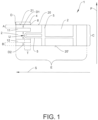
- the cooling device 1 is one that is used to cool electrical components 4, such as. B. laser diodes are provided to counteract overheating of the laser diodes 4 during operation.
- An essential component of the cooling device 1 is a base body 2, in which cooling channels 5, in particular micro-cooling channels, run.
- the base body 2 is preferably made of a metal, for example copper.
- an inlet and an outlet are provided on the base body 2, via which a fluid, in particular a coolant, can be introduced and removed during operation.
- an outside 20 comprises a connection area 21 to which the laser diode 4 with the thickness D is connected, for example by means of a solder material 8.
- the cooling channel 5 runs at least partially below the connection area 21 and the connection area 21, viewed in a primary direction P preferably terminates with an edge of the base body 2 in a secondary direction S running perpendicular to the primary direction P.
- the primary direction P runs in particular perpendicular to the plane along which the connection region 21 or the outside 20 of the cooling device 1 extends.
- a deflection area U of the cooling channel 5 is arranged below the connection area 21, viewed in the primary direction P. This allows a cooling fluid in the cooling channel 5 to be brought as close as possible to the connection area 21 and thus to the laser diode 4.
- a first stabilization layer 11, if necessary, and a second stabilization layer 12 are preferably provided, with which an adaptation of the expansion coefficient of the base body 2 to the expansion coefficient of the laser diode 4 is realized.
- the first stabilization layer 11, the second stabilization layer 12 and the connection region 21 lie one above the other.
- the first stabilization layer 11 is offset from the outside 20 or the connection area 21 by a distance A measured parallel to the primary direction P into the interior of the base body 2.
- the connection of the laser diode 4 it is not necessary to connect the first stabilization layer 11 and the second stabilization layer 12 to the outside 20 or as an intermediate layer between the base body 2 and the laser diode 4, so that the manufacturing effort is reduced.
- the arrangement offset from the outside 20 allows the laser diode 4 to be electrically contacted directly via the base body 2.
- first stabilization layer 11 and/or the second stabilization layer 12 comprise diamond or silicon carbide (SiC) or are made from it. This advantageously allows the largest possible heat spread to be achieved.
- first stabilization layer 11 and the second stabilization layer 12 are made of the same material.
- the second stabilization layer 12 is offset from a further outside 20 'opposite the outside 20 by the further distance B into the interior of the base body 2, the distance A preferably corresponding to the further distance B .
- a layer thickness measured in the primary direction P corresponds to D1 the first stabilization layer 11 of the layer thickness D2 of the second stabilization layer 12.
- the first stabilization layer 11 and the second stabilization layer 12 correspond to each other in shape and preferably in material composition, but are integrated into the base body 2 on opposite sides, the distance A the first stabilization layer 11 to the outside 20 corresponds to the further distance B of the second stabilization layer 12 to the further outside 20 '.
- the first stabilization layer 11, the second stabilization layer 12 and the connection surface 21 are arranged congruently with one another when viewed in the primary direction P, i.e. H. the first stabilization layer 11 and the second stabilization layer 12 extend in a plane perpendicular to the primary direction P or along the secondary direction S only as far as is predetermined by the connection surface 21.
- the first stabilization layer 11, the second stabilization layer 12 and the connection surface 21 are flush with the base body 2 when viewed along a secondary direction S, i.e. H. the first stabilization layer 11, the second stabilization layer 12 and the connection surface 21 are arranged on the edge of the base body.
- the cooling channel 5 extends at least partially between the first stabilization layer 11 and the second stabilization layer 12.
- a ratio of a length L1 of the cooling channel 5 measured along the secondary direction S, which is arranged between the first stabilization layer 11 and the second stabilization layer 12 as seen in the primary direction P, to the length L1 of the first stabilization layer 11 measured along the secondary direction S takes a value between 0.2 and 0.8, preferably between 0.5 and 0.75 and particularly preferably between 0.6 and 0.7.
- the base body 2 has a height C measured along the primary direction P, which is more than twice, preferably more than four times and particularly preferably more than 6 times as large as the thickness D of the laser diode 4 measured in the same direction.
- the Base body 2 has a longitudinal extension E measured along the secondary direction S, which is more than three times, more than five times and particularly preferably more than eight times as large as the third length L3 of the laser diode 4 measured along the secondary direction S.
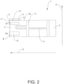
- FIG 2 1 shows a cooling device 1 according to a second preferred embodiment of the present invention.
- the embodiment shown differs from the one shown Figure 1 essentially only in that the second stabilization layer 12 differs from the first stabilization layer 11.
- the second stabilization layer 12 comprises another material instead of diamond or silicon carbonate (SiC), such as. B. molybdenum or tungsten.
- SiC silicon carbonate
- the layer thickness D2 of the second stabilization layer 12 and preferably the further distance B to the further outside 20' are adjusted accordingly.
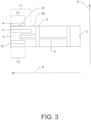
- Figure 3 1 shows a cooling device 1 according to a second preferred embodiment of the present invention.
- the embodiment shown differs from the one shown Figure 1 essentially only to the extent that the first stabilization layer 11 extends further in the secondary direction S than a third length L3 of the laser diode 4 or the connection surface 21.
- a ratio between a third length L3 of the connection surface 21 measured along the secondary direction S to the first Length L1 of the first stabilization layer 11 has a value between 0.33 and 0.99, preferably between 0.5 and 0.98 and particularly preferably between 0.66 and 0.95.
- the second stabilization layer 12 extends along the secondary direction S over a second length L2.
Landscapes
- Physics & Mathematics (AREA)
- Condensed Matter Physics & Semiconductors (AREA)
- General Physics & Mathematics (AREA)
- Electromagnetism (AREA)
- Optics & Photonics (AREA)
- Cooling Or The Like Of Semiconductors Or Solid State Devices (AREA)
- Semiconductor Lasers (AREA)
Description
- Die vorliegende Erfindung betrifft eine Kühlvorrichtung zum Kühlen eines elektrischen bzw. elektronischen Bauteils, insbesondere einer Laserdiode, und ein Verfahren zur Herstellung einer Kühlvorrichtung.
- Solche Kühlvorrichtungen sind beispielsweise aus der
JP 2016 115 767 A - Um für eine gewünschte Geradlinigkeit der Einzelemitter in einem Laserdiodenbarren zu sorgen, kennt der Stand der Technik Stabilisierungsschichten bzw. Zwischenschichten zwischen Bauteil und Grundkörper, sogenannte Submounts, die zum Angleichen der Ausdehnungskoeffizienten an der Außenseite des Grundkörpers befestigt werden und als Sockel die Laserdiode tragen. Wie aus der
JP 2016 115 767 A - Die
CN 202 652 683 zeigt eine Kühlvorrichtung zum Kühlen eines elektrischen Bauteils mit einem Grundkörper mit einer Außenseite und mindestens einem integrierten Kühlkanal. Eine Anbindung erfolgt hier über eine Anbindungsfläche an der Außenseite des Grundkörpers. Aus derDE 203 02 430 U1 ist eine Halbleitervorrichtung bekannt, bei der ein Halbleiterelement über einen Zwischenträger an einem Kühlelement mit einem Kühlkanal angebunden ist. - Es ist somit eine Aufgabe der vorliegenden Erfindung, eine Kühlvorrichtung bereitzustellen, auf die sich die Laserdiode auf einfache Weise montieren lässt, wobei zudem dem "Smile" - Effekt entgegengewirkt werden soll.
- Diese Aufgabe wird gelöst durch eine Kühlvorrichtung gemäß Anspruch 1 und ein Verfahren gemäß Anspruch 14. Weitere Vorteile und Merkmale der Erfindung ergeben sich aus den Unteransprüchen sowie der Beschreibung und den beigefügten Figuren.
- Erfindungsgemäß ist eine Kühlvorrichtung zum Kühlen eines elektrischen Bauteils, insbesondere einer Laserdiode, vorgesehen, umfassend:
- ein Grundkörper mit mindestens einer Außenseite und mindestens einem integrierten Kühlkanal, insbesondere Mikrokühlkanal,
- eine Anbindungsfläche an der Außenseite des Grundkörpers zur Anbindung des elektrischen Bauteils an den Grundkörper und
- eine erste Stabilisierungsschicht,
- Gegenüber dem Stand der Technik hat sich in überraschender Weise herausgestellt, dass eine Anpassung der thermischen Ausdehnungskoeffizienten auch dann noch in einem ausreichenden Umfang erfolgen kann, wenn die erste Stabilisierungsschicht gegenüber der Anbindungsfläche erfindungsgemäß nach innen versetzt ist und nicht Teil der Außenseite des Grundkörper ist. Die Folge ist, dass eine Kühlvorrichtung bereitgestellt werden kann, in die bereits eine erste Stabilisierungsschicht integriert ist, so dass auf der Seite der Bauteilhersteller direkt eine unmittelbare Anbindung des elektrischen Bauteils, insbesondere der Laserdiode, erfolgen kann. Ein weiterer Vorteil besteht darin, dass die Integration der ersten Stabilisierungsschicht diese gegen Umwelteinflüsse schützt, z. B. vor Korrosionsschädigungen. Insbesondere ist es vorgesehen, dass das Bauteil ein Laserdiodenbarren mit mehreren Einzelemittern umfasst.
- Vorzugsweise ist es dabei vorgesehen, dass sich die Primärrichtung im Wesentlichen senkrecht zur Anbindungsfläche bzw. einer Außenseite des Grundkörpers erstreckt. Beispielsweise ist die Anbindungsfläche ein Teil einer sich entlang der Längserstreckung des Grundkörpers erstreckenden Außenseite. Insbesondere bildet die Anbindungsfläche weniger als ein Viertel dieser Außenseite. Ferner weist der Grundkörper einen Ein- und Ausgang auf, über die ein Kühlfluid in den Kühlkanal eingeleitet werden kann. Unter einem integrierten Kühlkanal ist vorzugsweise ein solcher Kühlkanal zu verstehen, der im Wesentlichen, d. h. insbesondere mit Ausnahme des Eingangs und Ausgangs, im Inneren des Grundkörpers verläuft. Insbesondere ist der Grundkörper aus einem Metall, vorzugsweise Kupfer, gefertigt, während die erste Stabilisierungsschicht aus einem anderen Material, insbesondere einem Nichtmetall, gefertigt ist. Ferner erstreckt sich die erste Stabilisierungsschicht im Wesentlichen parallel zur Anbindungsfläche. Es ist aber auch vorstellbar, dass die erste Stabilisierungsschicht schräg zur Außenseite verläuft.
- Gemäß einer weiteren Ausführungsform der vorliegenden Erfindung ist es vorgesehen, dass eine zweite Stabilisierungsschicht vorgesehen ist, wobei die erste Stabilisierungsschicht, die zweite Stabilisierungsschicht und die Anbindungsfläche entlang einer Primärrichtung zumindest teilweise übereinander angeordnet sind und die erste Stabilisierungsschicht näher an der Anbindungsfläche als die zweite Stabilisierungsschicht angeordnet ist. Mittels einer zweiten Stabilisierungsschicht lässt sich mit Vorteil einer Krümmung des Grundkörpers bei thermischer Beanspruchung und damit der Ausbildung eines "Smile"-Effekts entgegenwirken, wenn Einzelemitter eines Laserbarrens auf der Kühlvorrichtung angeordnet sind. Hierbei ist es vorzugsweise vorgesehen, dass die zweite Stabilisierungsschicht parallel zur Anbindungsfläche und/oder der ersten Stabilisierungsschicht verläuft. Es ist aber auch vorstellbar, dass die erste Stabilisierungsschicht und/oder zweite Stabilisierungsschicht schräg zur Außenseite verlaufen. Vorzugsweise ist die zweite Stabilisierungsschicht ebenfalls in den Grundkörper integriert. Insbesondere ist die zweite Stabilisierungsschicht gegenüber einer der Anbindungsfläche am Grundkörper gegenüberliegenden weiteren Außenseite um einen weiteren Abstand ins Innere des Grundkörpers versetzt.
- Insbesondere ist es vorgesehen, dass die erste Stabilisierungsschicht und die zweite Stabilisierungsschicht in Hinblick auf ihre Materialzusammensetzung und ihre geometrische Form einander entsprechen. Vorzugsweise entspricht dann der Abstand, d. h. eine Distanz zwischen der ersten Stabilisierungsschicht und der Außenseite, dem weiteren Abstand, d. h. einer Distanz zwischen der zweiten Stabilisierungsschicht und der weiteren Außenseite.
- Zweckmäßig ist es vorgesehen, dass der Abstand zwischen der Anbindungsfläche und der ersten Stabilisierungsschicht einen Wert zwischen 100 µm und 1000 µm, bevorzugt zwischen 150 µm und 750 µm und besonders bevorzugt zwischen 200 µm und 500 µm annimmt. Insbesondere hat sich für Abstandswerte zwischen 300 µm und 500 µm herausgestellt, dass eine in der Fertigung ausreichend stabiler Teil des Grundkörpers herstellen lässt und zudem ein möglichst großer Einfluss auf den Ausdehnungskoeffizienten im Bindungsbereich zwischen dem Bauteil und dem Grundkörper genommen werden kann.
- In einer weiteren Ausführungsform der vorliegenden Erfindung ist es vorgesehen, dass die erste Stabilisierungsschicht Diamant und/oder Siliziumkarbid umfasst. Denkbar sind auch andere Materialien mit hoher thermischer Leitfähigkeit wie z.B. AlN, BeO, W, Mo oder Si und/oder Komposite mit metallischer Matrix auf Basis von Cu oder Ag. Wegen der sehr hohen Wärmeleitfähigkeit erweist sich eine erste Stabilisierungsschicht aus Diamant und/oder Siliziumkarbid als besonders vorteilhaft für die Wärmespreizung beim Wärmetransport vom Wärme entwickelnden elektrischen Bauteil zum Kühlkanal bzw. in den Grundkörper. Weiterhin ist es vorstellbar, dass die erste Stabilisierungsschicht und/oder die zweite Stabilisierungsschicht in Primärrichtung und/oder Sekundärrichtung gesehen durchgehend oder unterbrochen ist. Ferner ist es denkbar, dass mehrere erste Stabilisierungsschichten und/oder mehrere zweite Stabilisierungsschichten in Primärrichtung gesehen übereinanderliegend angeordnet sind.
- Vorzugsweise ist es vorgesehen, dass die erste Stabilisierungsschicht und die Anbindungsfläche in Primärrichtung gesehen deckungsgleich zueinander angeordnet sind. Unter "deckungsgleich" ist insbesondere zu verstehen, dass die erste Stabilisierungsschicht in einer senkrecht zur Primärrichtung verlaufenden Sekundärrichtung gesehen die Anbindungsfläche bzw. die Laserdiode nicht überragt bzw. bündig mit ihr abschließt. Vorzugsweise entsprechen die in einer senkrecht zur Primärrichtung bemessenen Ausdehnungen bzw. Flächen der Anbindungsfläche einerseits und der Sekundärschicht anderseits einander. Denkbar ist auch, dass die zweite Stabilisierungsschicht deckungsgleich zur Anbindungsfläche und/oder der ersten Stabilisierungsfläche angeordnet ist. Insbesondere ist es vorgesehen, dass sich die erste Stabilisierungsschicht und/oder die zweite Stabilisierungsschicht nicht über die gesamte Länge bzw. gesamte Längserstreckung der Kühlvorrichtung entlang der Sekundärrichtung erstreckt. Dadurch lassen sich mit Vorteil der Material- und der damit einhergehenden Kostenmehraufwand für die erste Stabilisierungsschicht und die zweite Stabilisierungsschicht reduzieren. Insbesondere verläuft die Sekundärrichtung parallel zur Längsrichtung bzw. -erstreckung des Grundkörpers.
- Vorzugsweise ist es vorgesehen, dass zwischen der ersten Stabilisierungsschicht und der zweiten Stabilisierungsschicht in Primärrichtung gesehen mindestens ein Teilbereich des Kühlkanals verläuft. Dadurch lässt sich mit Vorteil das Kühlfluid möglichst nah an die zu kühlende Laserdiode heranführen. Beispielsweise ist ein Umlenkbereich des Kühlkanals in Primärrichtung gesehen unterhalb der Anbindungsfläche angeordnet. Vorzugsweise nimmt ein Verhältnis einer entlang der Sekundärrichtung bemessenen Länge desjenigen Teilbereich des Kühlkanals, der in Primärrichtung gesehen zwischen der ersten Stabilisierungsschicht und der zweiten Stabilisierungsschicht angeordnet ist, zur entlang der Sekundärrichtung bemessenen Länge der ersten Stabilisierungsschicht einen Wert zwischen 0,2 und 0,8, bevorzugt zwischen 0,5 und 0,75 und besonders bevorzugt zwischen 0,6 und 0,7 an. Insbesondere bei einem Verhältnis zwischen 0,6 und 0,7 hat sich gezeigt, dass eine möglichst gleichmäßige Kühlung des Bauteils durch den Kühlkanal realisierbar ist.
- Insbesondere ist es vorgesehen, dass sich die erste Stabilisierungsschicht entlang einer senkrecht zur Primärrichtung verlaufenden Sekundärrichtung über eine erste Länge erstreckt, wobei sich die zweite Stabilisierungsschicht entlang der Sekundärrichtung über eine zweite Länge erstreckt und die Anbindungsfläche sich entlang der Sekundärrichtung über eine dritte Länge erstreckt, wobei das Verhältnis der ersten Länge und/oder der zweiten Länge zur dritten Länge einen Wert zwischen 0,5 und 6,0 annimmt, vorzugsweise einen Wert zwischen 0,5 und 3,0, bevorzugt einen Wert zwischen 0,9 und 2,0 und besonders bevorzugt zwischen 0,95 und 1,5 annimmt. Dadurch erstreckt sich die erste Stabilisierungsschicht bzw. die zweite Stabilisierungsschicht in Sekundärrichtung gesehen weiter als die Anbindungsfläche. Insbesondere mit Diamant bzw. Siliziumkarbid als Materialien für die erste Stabilisierungsschicht und die zweite Stabilisierungsschicht lässt sich durch diese gegenüber der dritten Länge größer gewählte Länge eine weitere Wärmeaufspreizung im Grundkörper realisieren. Vorzugweise ist es vorgesehen, dass die erste Länge und/oder die zweite Länge einen Wert zwischen 5 und 25 mm bevorzugt zwischen 6 und 18 mm und besonders bevorzugt zwischen 7 und 15 mm annimmt. Vorzugsweise nimmt ein Verhältnis zwischen der entlang der Sekundärrichtung S bemessenen dritten Länge der Anbindungsfläche zu der ersten Länge der ersten Stabilisierungsschicht einen Wert zwischen 0,33 und 0,99, bevorzugt zwischen 0,5 und 0,98 und besonders bevorzugt zwischen 0,66 und 0,95 an.
- Zweckmäßig ist es vorgesehen, dass sich die erste Stabilisierungsschicht von der zweiten Stabilisierungsschicht unterscheidet, insbesondere in Hinblick auf die Position innerhalb des Grundkörpers, ihre Materialzusammensetzung und/oder ihre Ausdehnung , insbesondere Dicke, in einer parallel zur Primärrichtung verlaufenden Richtung. Dadurch ist es beispielsweise möglich, in die erste Stabilisierungsschicht Diamant und/oder Siliziumkarbid zu integrieren, während die zweite Stabilisierungsschicht Molybdän, Wolfram, Silizium, ein Laminat, CuW, CuMo oder eine Keramik bzw. ein Glas aufweist. Dadurch lassen sich Zusatzkosten für die zweite Stabilisierungsschicht steuern bzw. gering halten. Um dennoch in Primärrichtung gesehen eine Symmetrisierung des thermischen Ausdehnungskoeffizienten zu realisieren und so einem Durchbiegen des Grundkörpers entgegenzuwirken, ist es mit Vorteil vorgesehen, dass die zweite Stabilisierungsschicht entsprechend, d. h. in Hinblick auf Dimensionierung und Position der zweiten Stabilisierungsschicht, modifiziert wird.
- Vorzugsweise ist es vorgesehen, dass die erste Länge und/oder die dritte Länge größer ist als ein in Primärrichtung bemessener Abstand zwischen der ersten Stabilisierungsschicht und der Anbindungsfläche.
- Ein weiterer Aspekt der vorliegenden Erfindung ist ein Verfahren zur Herstellung einer Kühlvorrichtung gemäß einem der vorhergehenden Ansprüche, wobei die erste und/oder die zweite Stabilisierungsschicht mittels eines Aktivlot-Verfahrens an den Grundkörper angebunden werden. Alle für die erfindungsgemäße Kühlvorrichtung beschriebenen Merkmale und deren Vorteile lassen sich sinngemäß ebenfalls auf das erfindungsgemäße Verfahren übertragen und andersherum.
- Unter einem Aktivlot-Verfahren z. B. zum Verbinden von Metallschichten oder Metallfolien, insbesondere auch von Kupferschichten oder Kupferfolien mit Keramikmaterial ist ein Verfahren zu verstehen, welches speziell auch zum Herstellen von Metall-Keramik-Substraten verwendet wird, wird bei einer Temperatur zwischen ca.650-1000°C eine Verbindung zwischen einer Metallfolie, beispielsweise Kupferfolie, und einem Keramiksubstrat, beispielsweise Aluminiumnitrid-Keramik, unter Verwendung eines Hartlots hergestellt, welches zusätzlich zu einer Hauptkomponente, wie Kupfer, Silber und/oder Gold auch ein Aktivmetall enthält. Dieses Aktivmetall, welches beispielsweise wenigstens ein Element der Gruppe Hf, Ti, Zr, Nb, Ce ist, stellt durch chemische Reaktion eine Verbindung zwischen dem Lot und der Keramik her, während die Verbindung zwischen dem Lot und dem Metall eine metallische Hartlöt-Verbindung ist. Mittels des Aktivlotverfahrens ist es mit Vorteil möglich Diamant und/oder Siliziumkarbonat an den Grundkörper anzubinden.
- Es zeigt:
- Fig.1:
- eine Kühlvorrichtung gemäß einer ersten bevorzugten Ausführungsform der vorliegenden Erfindung
- Fig. 2:
- eine Kühlvorrichtung gemäß einer zweiten bevorzugten Ausführungsform der vorliegenden Erfindung und
- Fig.3
- eine Kühlvorrichtung gemäß einer dritten bevorzugten Ausführungsform der vorliegenden Erfindung
- In der
Figur 1 ist eine Kühlvorrichtung 1 gemäß einer ersten beispielhaften Ausführungsform der vorliegenden Erfindung dargestellt. Insbesondere handelt es sich bei der Kühlvorrichtung 1 um eine solche, die zum Kühlen von elektrischen Bauteilen 4, wie z. B. Laserdioden, vorgesehen sind, um einem Überhitzen der Laserdioden 4 im Betrieb entgegenzuwirken. Wesentliche Bestandteile der Kühlvorrichtung 1 ist ein Grundkörper 2, in dem Kühlkanäle 5, insbesondere Mikrokühlkanäle, verlaufen. Dabei ist der Grundkörper 2 vorzugsweise aus einem Metall, beispielsweise Kupfer, gefertigt. Ferner ist am Grundkörper 2 ein Eingang und ein Ausgang vorgesehen, über den ein Fluid, insbesondere eine Kühlflüssigkeit, im Betrieb ein- und ausgeleitet werden kann. - Ferner umfasst eine Außenseite 20 einen Anbindungsbereich 21, an dem die Laserdiode 4 mit der Dicke D angebunden ist, beispielsweise mittels eines Lotmaterials 8. In dem dargestellten Ausführungsbeispiel verläuft der Kühlkanal 5 in einer Primärrichtung P gesehen zumindest teilweise unterhalb des Anbindungsbereichs 21 und der Anbindungsbereich 21 schließt vorzugsweise mit einer Kante des Grundkörpers 2 in einer senkrecht zur Primärrichtung P verlaufenden Sekundärrichtung S ab. Dabei verläuft die Primärrichtung P insbesondere senkrecht zu derjenigen Ebene, entlang der sich der Anbindungsbereich 21 bzw. die Außenseite 20 der Kühlvorrichtung 1 erstreckt. Vorzugsweise ist ein Umlenkbereich U des Kühlkanals 5 in Primärrichtung P gesehen unterhalb des Anbindungsbereichs 21 angeordnet. Dadurch lässt sich ein kühlendes Fluid im Kühlkanal 5 möglichst nah an den Anbindungsbereich 21 und somit an die Laserdiode 4 heranführen.
- Wegen der unterschiedlichen thermischen Ausdehnungskoeffizienten im Grundkörper 2 einerseits und des elektrischen Bauteils 4 andererseits können mechanische Spannungen entstehen, die mitunter zu einer Verformung des Anbindungsbereichs 21 bzw. der Laserdiode 4 führen können. Da solche Geometrieänderungen unmittelbar den "Smile" -Effekt verursachen, ist es von Vorteil, diese mechanischen Spannungen zu unterdrücken. Hierzu sind vorzugsweise eine erste Stabilisierungsschicht 11 ggf. und eine zweite Stabilisierungsschicht 12 vorgesehen, mit denen eine Anpassung des Ausdehnungskoeffizienten des Grundkörpers 2 an den Ausdehnungskoeffizienten der Laserdiode 4 realisiert wird. Dabei ist es insbesondere vorgesehen dass in Primärrichtung P gesehen, die erste Stabilisierungsschicht 11, die zweite Stabilisierungsschicht 12 und der Anbindungsbereich 21 übereinanderliegen.
- Um eine Kühlvorrichtung 1 bereitzustellen, bei der die Laserdiode 4 unmittelbar, d. h. ohne die Anbindung von Zwischenelementen an der Außenseite 20, angebunden werden kann, ist es vorgesehen, dass die erste Stabilisierungsschicht 11 gegenüber der Außenseite 20 bzw. dem Anbindungsbereich 21 um einen parallel zur Primärrichtung P bemessenen Abstand A ins Innere des Grundkörpers 2 versetzt ist. Mit anderen Worten: für die Anbindung der Laserdiode 4 ist es nicht erforderlich die erste Stabilisierungsschicht 11 und die zweite Stabilisierungsschicht 12 an der Außenseite 20 bzw. als Zwischenschicht zwischen den Grundkörper 2 und die Laserdiode 4 anzubinden, so dass der Fertigungsaufwand reduziert wird. Außerdem erlaubt die gegenüber der Außenseite 20 versetzte Anordnung, dass die Laserdiode 4 unmittelbar über den Grundkörper 2 elektrisch kontaktiert werden kann.
- Vorzugsweise ist es vorgesehen, dass die erste Stabilisierungsschicht 11 und/oder die zweite Stabilisierungsschicht 12 Diamant oder Siliziumkarbid (SiC) umfassen oder daraus gefertigt sind. Dadurch lässt sich mit Vorteil eine möglichst große Wärmespreizung realisieren. Insbesondere sind in der Ausführungsform in
Figur 1 die erste Stabilisierungsschicht 11 und die zweite Stabilisierungsschicht 12 aus demselben Material gefertigt. Um im Grundkörper 2 eine bevorzugt symmetrische Veränderungen des Ausdehnungskoeffizienten zu veranlassen, ist die zweite Stabilisierungsschicht 12 gegenüber einer der Außenseite 20 gegenüberliegenden weiteren Außenseite 20' um den weiteren Abstand B ins Innere des Grundkörper 2 hineinversetzt, wobei der Abstand A vorzugsweise dem weiteren Abstand B entspricht. Zudem entspricht eine in Primärrichtung P bemessene Schichtdicke D1 der ersten Stabilisierungsschicht 11 der Schichtdicke D2 der zweiten Stabilisierungsschicht 12. Mit anderen Worten: die erste Stabilisierungsschicht 11 und die zweite Stabilisierungsschicht 12 entsprechen einander in Form und vorzugsweise in der Materialzusammensetzung, sind aber auf gegenüberliegenden Seiten in den Grundkörper 2 integriert, wobei der Abstand A der ersten Stabilisierungsschicht 11 zur Außenseite 20 dem weiteren Abstand B der zweiten Stabilisierungsschicht 12 zur weiteren Außenseite 20' entspricht. - Um einen Materialaufwand für die erste Stabilisierungsschicht 11 und die zweite Stabilisierungsschicht 12 möglichst gering zu halten, ist es vorzugsweise vorgesehen, dass die erste Stabilisierungsschicht 11, die zweite Stabilisierungsschicht 12 und die Anbindungsfläche 21 in Primärrichtung P gesehen deckungsgleich zueinander angeordnet sind, d. h. die erste Stabilisierungsschicht 11 und die zweite Stabilisierungsschicht 12 erstrecken sich in einer senkrecht zur Primärrichtung P verlaufenden Ebene bzw. entlang der Sekundärrichtung S nur soweit wie es durch die Anbindungsfläche 21 vorgegeben ist. Insbesondere ist es vorgesehen, dass die erste Stabilisierungsschicht 11, die zweite Stabilisierungsschicht 12 und die Anbindungsfläche 21 entlang einer Sekundärrichtung S gesehen bündig mit dem Grundkörper 2 abschließen, d. h. die erste Stabilisierungsschicht 11, die zweite Stabilisierungsschicht 12 und die Anbindungsfläche 21 sind am Rand des Grundkörper angeordnet.
- Weiterhin ist es vorgesehen, dass sich der Kühlkanal 5 zumindest teilweise zwischen der ersten Stabilisierungsschicht 11 und der zweiten Stabilisierungsschicht 12 erstreckt. Vorzugsweise nimmt ein Verhältnis einer entlang der Sekundärrichtung S bemessenen Länge desjenigen Teilabschnitts T des Kühlkanals 5, der in Primärrichtung P gesehen zwischen der ersten Stabilisierungsschicht 11 und der zweiten Stabilisierungsschicht 12 angeordnet ist, zur entlang der Sekundärrichtung S bemessenen Länge L1 der ersten Stabilisierungsschicht 11 einen Wert zwischen 0,2 und 0,8, bevorzugt zwischen 0,5 und 0,75 und besonders bevorzugt zwischen 0,6 und 0,7 an.
- Zudem weist der Grundkörper 2 eine entlang der Primärrichtung P bemessene Höhe C auf, die mehr als doppelt, vorzugsweise mehr als vierfach und besonders bevorzugt mehr als 6-mal so groß ist wie die in dieselbe Richtung bemessene Dicke D der Laserdiode 4. Außerdem hat der Grundkörper 2 eine entlang der Sekundärrichtung S bemessene Längserstreckung E, die mehr als dreimal, mehr als fünfmal und besonders bevorzugt mehr als achtmal so groß ist wie die entlang der Sekundärrichtung S bemessene dritte Länge L3 der Laserdiode 4.
- In
Figur 2 ist eine Kühlvorrichtung 1 gemäß einer zweiten bevorzugten Ausführungsform der vorliegenden Erfindung dargestellt. Dabei unterscheidet sich die dargestellte Ausführungsform von derjenigen ausFigur 1 im Wesentlichen nur dahingehend, dass sich die zweite Stabilisierungsschicht 12 von der ersten Stabilisierungsschicht 11 unterscheidet. Vorzugsweise umfasst die zweite Stabilisierungsschicht 12 statt Diamant oder Siliziumkarbonat (SiC) ein anderes Material, wie z. B. Molybdän oder Wolfram. Um dennoch für einen gegenüber der Primärrichtung P symmetrische Ausdehnungskoeffizienten zu sorgen, sind die Schichtdicke D2 der zweiten Stabilisierungsschicht 12 und vorzugsweise der weitere Abstand B zur weiteren Außenseite 20` entsprechend angepasst. - In
Figur 3 ist eine Kühlvorrichtung 1 gemäß einer zweiten bevorzugten Ausführungsform der vorliegenden Erfindung dargestellt. Dabei unterscheidet sich die dargestellte Ausführungsform von derjenigen ausFigur 1 im Wesentlichen nur dahingehend, dass sich die erste Stabilisierungsschicht 11 in Sekundärrichtung S weiter erstreckt als eine dritter Länge L3 der Laserdiode 4 bzw. der Anbindungsfläche 21. Vorzugsweise nimmt ein Verhältnis zwischen einer entlang der Sekundärrichtung S bemessenen dritten Länge L3 der Anbindungsfläche 21 zu der ersten Länge L1 der ersten Stabilisierungsschicht 11 einen Wert zwischen 0,33 und 0,99, bevorzugt zwischen 0,5 und 0,98 und besonders bevorzugt zwischen 0,66 und 0,95 an. Ferner erstreckt sich die zweite Stabilisierungsschicht 12 entlang der Sekundärrichtung S über eine zweite Länge L2 erstreckt. -
- 1
- Kühlvorrichtung
- 2
- Grundkörper
- 4
- elektrisches Bauteil (z. B. Laseriode)
- 5
- Kühlkanal
- 8
- Lotmaterial
- 11
- erste Stabilisierungsschicht
- 12
- zweite Stabilisierungsschicht
- 20
- Außenseite
- 20'
- weiteren Außenseite
- 21
- Anbindungsfläche
- A
- Abstand
- B
- weiterer Abstand
- C
- Höhe des Grundkörpers
- D
- Schichtdicke der Laserdiode
- D1
- Schichtdicke der ersten Stabilisierungsschicht
- D2
- Schichtdicke der zweiten Stabilisierungsschicht
- L1
- erste Länge
- L2
- zweite Länge
- L3
- dritte Länge
- E
- Längserstreckung des Grundkörpers
- P
- Primärrichtung
- S
- Sekundärrichtung
- T
- Teilabschnitt
- U
- Umlenkbereich
Claims (14)
- Kühlvorrichtung (1) zum Kühlen einer Laserdiode, umfassend:- ein Grundkörper (2) mit einer Außenseite (20) und mindestens einem integrierten Kühlkanal (5), insbesondere Mikrokühlkanal,- eine Anbindungsfläche (21) an der Außenseite (20) des Grundkörpers (2) zur Anbindung des elektrischen Bauteils (4) an den Grundkörper (2) und- eine erste Stabilisierungsschicht (11),wobei die erste Stabilisierungsschicht (11) und die Anbindungsfläche (21) entlang einer Primärrichtung (P) übereinander angeordnet sind, undwobei die erste Stabilisierungsschicht (11) gegenüber der Anbindungsfläche um einen Abstand (A) entlang einer parallel zur Primärrichtung (P) verlaufenden Richtung ins Innere des Grundkörpers (2) versetzt ist.
- Kühlvorrichtung (1) gemäß Anspruch 1, wobei eine zweite Stabilisierungsschicht (12) vorgesehen ist, wobei die erste Stabilisierungsschicht (11), die zweite Stabilisierungsschicht (12) und die Anbindungsfläche (21) entlang einer Primärrichtung (P) übereinander angeordnet sind und wobei die erste Stabilisierungsschicht (11) näher an der Anbindungsfläche (21) als die zweite Stabilisierungsschicht (12) angeordnet ist.
- Kühlvorrichtung (1) gemäß Anspruch 1 oder 2, wobei der Abstand (A) zwischen der Anbindungsfläche (21) und der ersten Stabilisierungsschicht (11) einen Wert zwischen 100 µm und 1000 µm, bevorzugt zwischen 150 µm und 750 µm und besonders bevorzugt zwischen 200 µm und 500 µm annimmt.
- Kühlvorrichtung (1) gemäß einem der vorhergehenden Ansprüche, wobei die erste Stabilisierungsschicht (11) Diamant umfasst.
- Kühlvorrichtung (1) gemäß einem der vorhergehenden Ansprüche, wobei die erste Stabilisierungsschicht Siliziumkarbid umfasst.
- Kühlvorrichtung (1) gemäß einem der vorhergehenden Ansprüche, wobei die erste Stabilisierungsschicht (11) und die Anbindungsfläche (21) in Primärrichtung (P) gesehen deckungsgleich zueinander angeordnet sind.
- Kühlvorrichtung (1) gemäß einem der vorhergehenden Ansprüche, wobei sich die erste Stabilisierungsschicht (11) entlang einer senkrecht zur Primärrichtung (P) verlaufenden Sekundärrichtung (S) über eine erste Länge (L1) erstreckt, wobei sich die zweite Stabilisierungsschicht (12) entlang der Sekundärrichtung (S) über eine zweite Länge (L2) erstreckt und die Anbindungsfläche (21) sich entlang der Sekundärrichtung (S) über eine dritte Länge (L3) erstreckt, wobei das Verhältnis der ersten Länge (L1) und/oder der zweiten Länge (L2) zur dritten Länge (L3) einen Wert zwischen 0,5 und 6,0 annimmt, vorzugsweise einen Wert zwischen 0,5 und 3,0, bevorzugt einen Wert zwischen 0,9 und 2,0 und besonders bevorzugt zwischen 0,95 und 1,5 annimmt.
- Kühlvorrichtung (1) gemäß einem der vorhergehenden Ansprüche, wobei die erste Länge (L1) und/oder die zweite Länge (L2) einen Wert zwischen 5 und 25 mm bevorzugt zwischen 6 und 18 mm und besonders bevorzugt zwischen 7 und 15 mm annimmt.
- Kühlvorrichtung gemäß einem der vorhergehenden Ansprüche, wobei sich die erste Stabilisierungsschicht (11) und/oder die zweite Stabilisierungsschicht (12) nicht über die gesamte Längserstreckung der Kühlvorrichtung (1) entlang der Sekundärrichtung (S) erstreckt.
- Kühlvorrichtung (1) gemäß einem der vorhergehenden Ansprüche, wobei ein Verhältnis zwischen einer entlang der Sekundärrichtung (S) bemessenen dritten Länge (L3) der Anbindungsfläche (21) zu der ersten Länge (L1) der ersten Stabilisierungsschicht (11) einen Wert zwischen 0,33 und 0,99, bevorzugt zwischen 0,5 und 0,98 und besonders bevorzugt zwischen 0,66 und 0,95 annimmt.
- Kühlvorrichtung (1) gemäß einem der vorhergehenden Ansprüche, wobei zwischen der ersten Stabilisierungsschicht (11) und der zweiten Stabilisierungsschicht (12) in Primärrichtung (P) gesehen ein Teilbereich (T) des Kühlkanals (5) verläuft.
- Kühlvorrichtung (1) gemäß einem der vorhergehenden Ansprüche, wobei sich die erste Stabilisierungsschicht (11) von der zweiten Stabilisierungsschicht (12) unterscheidet, insbesondere in Hinblick auf die Position innerhalb des Grundkörpers (2), ihrer Materialzusammensetzung und/oder ihrer Dicke (D1, D2) in einer parallel zur Primärrichtung (P) verlaufenden Richtung.
- Kühlvorrichtung (1) gemäß einem der vorhergehenden Ansprüche, wobei die erste Länge (L1) und/oder die dritte Länge (L3) größer ist als der in Primärrichtung (P) bemessene Abstand (A) zwischen der ersten Stabilisierungsschicht (11) und der Anbindungsfläche (21).
- Verfahren zur Herstellung einer Kühlvorrichtung (1) gemäß einem der vorhergehenden Ansprüche, wobei die erste Stabilisierungsschicht (11) und/oder die zweite Stabilisierungsschicht (12) mittels eines AMB-Verfahrens an den Grundkörper (2) angebunden werden.
Applications Claiming Priority (2)
| Application Number | Priority Date | Filing Date | Title |
|---|---|---|---|
| DE102017122575.7A DE102017122575B3 (de) | 2017-09-28 | 2017-09-28 | Kühlvorrichtung zum Kühlen eines elektrischen Bauteils und Verfahren zur Herstellung einer Kühlvorrichtung |
| PCT/EP2018/073836 WO2019063251A1 (de) | 2017-09-28 | 2018-09-05 | Kühlvorrichtung zum kühlen eines elektrischen bauteils und verfahren zur herstellung einer kühlvorrichtung |
Publications (2)
| Publication Number | Publication Date |
|---|---|
| EP3688848A1 EP3688848A1 (de) | 2020-08-05 |
| EP3688848B1 true EP3688848B1 (de) | 2024-01-03 |
Family
ID=65321971
Family Applications (1)
| Application Number | Title | Priority Date | Filing Date |
|---|---|---|---|
| EP18772749.0A Active EP3688848B1 (de) | 2017-09-28 | 2018-09-05 | Kühlvorrichtung zum kühlen eines elektrischen bauteils und verfahren zur herstellung einer kühlvorrichtung |
Country Status (5)
| Country | Link |
|---|---|
| US (1) | US11552446B2 (de) |
| EP (1) | EP3688848B1 (de) |
| CN (1) | CN111149264A (de) |
| DE (1) | DE102017122575B3 (de) |
| WO (1) | WO2019063251A1 (de) |
Family Cites Families (15)
| Publication number | Priority date | Publication date | Assignee | Title |
|---|---|---|---|---|
| DE19605302A1 (de) | 1996-02-14 | 1997-08-21 | Fraunhofer Ges Forschung | Kühlkörper mit einer Montagefläche für ein elektronisches Bauteil |
| DE19956565B4 (de) * | 1999-11-24 | 2006-03-30 | Laserline Gesellschaft für Entwicklung und Vertrieb von Diodenlasern mbH | Verfahren zum Herstellen einer Wärmesenke für elektrische Bauelemente |
| DE10234704A1 (de) * | 2002-07-30 | 2004-02-19 | Osram Opto Semiconductors Gmbh | Halbleitervorrichtung mit Kühlelement |
| JP4002234B2 (ja) * | 2003-12-16 | 2007-10-31 | 浜松ホトニクス株式会社 | 半導体レーザ装置及びその製造方法 |
| US20060045153A1 (en) * | 2004-08-31 | 2006-03-02 | Carter Serrena M | Low thermal expansion coefficient cooler for diode-laser bar |
| US7305016B2 (en) | 2005-03-10 | 2007-12-04 | Northrop Grumman Corporation | Laser diode package with an internal fluid cooling channel |
| US20080056314A1 (en) * | 2006-08-31 | 2008-03-06 | Northrop Grumman Corporation | High-power laser-diode package system |
| DE102008001226A1 (de) * | 2007-04-24 | 2008-10-30 | Ceramtec Ag | Bauteil mit einem metallisierten Keramikkörper |
| US8243766B2 (en) * | 2007-09-21 | 2012-08-14 | Michael Huff | Means for improved implementation of laser diodes and laser diode arrays |
| JP2012019086A (ja) * | 2010-07-08 | 2012-01-26 | Sony Corp | ヒートシンクおよびその製造方法並びに半導体レーザ装置 |
| CN103155310B (zh) | 2010-10-15 | 2015-02-11 | 浜松光子学株式会社 | 半导体激光装置 |
| CN202652683U (zh) * | 2011-11-27 | 2013-01-02 | 葛豫卿 | 一种带液/汽相变传热基板的印刷电路板 |
| EP3171465B1 (de) * | 2014-07-14 | 2019-09-25 | Panasonic Intellectual Property Management Co., Ltd. | Gekühlte halbleiterlaservorrichtung |
| JP6573451B2 (ja) | 2014-12-12 | 2019-09-11 | 浜松ホトニクス株式会社 | 半導体レーザユニット及び半導体レーザ装置 |
| WO2017183300A1 (ja) * | 2016-04-19 | 2017-10-26 | パナソニックIpマネジメント株式会社 | 半導体レーザ装置及びその製造方法 |
-
2017
- 2017-09-28 DE DE102017122575.7A patent/DE102017122575B3/de not_active Expired - Fee Related
-
2018
- 2018-09-05 CN CN201880063734.0A patent/CN111149264A/zh active Pending
- 2018-09-05 WO PCT/EP2018/073836 patent/WO2019063251A1/de not_active Ceased
- 2018-09-05 EP EP18772749.0A patent/EP3688848B1/de active Active
- 2018-09-05 US US16/651,464 patent/US11552446B2/en active Active
Also Published As
| Publication number | Publication date |
|---|---|
| DE102017122575B3 (de) | 2019-02-28 |
| US11552446B2 (en) | 2023-01-10 |
| EP3688848A1 (de) | 2020-08-05 |
| CN111149264A (zh) | 2020-05-12 |
| US20200266606A1 (en) | 2020-08-20 |
| WO2019063251A1 (de) | 2019-04-04 |
Similar Documents
| Publication | Publication Date | Title |
|---|---|---|
| EP2814788B1 (de) | Metall-keramik-substrat sowie verfahren zum herstellen eines derartigen metall-keramik-substrates | |
| EP3559989B1 (de) | Trägersubstrat für elektrische bauteile und verfahren zur herstellung eines trägersubstrats | |
| DE102009033029A1 (de) | Elektronische Vorrichtung | |
| EP2447235A1 (de) | Metall-Keramik-Substrat sowie Verfahren zum Herstellen eines solchen Substrates | |
| EP1124259A2 (de) | Kühlvorrichtung für ein Hochleistungs-Halbleitermodul | |
| DE102007030389A1 (de) | Wärmesenke sowie Bau- oder Moduleinheit mit einer Wärmesenke | |
| EP3208841B1 (de) | Verfahren zur herstellung einer wärmespreizplatte, wärmespreizplatte, verfahren zur herstellung eines halbleitermoduls und halbleitermodul | |
| DE102016121322A1 (de) | Basiseinheit für ein Leistungsmodul | |
| EP3555913B1 (de) | Halbleitermodul mit bodenplatte mit hohlwölbung | |
| DE102021125557A1 (de) | Metall-Keramik-Substrat und Verfahren zur Herstellung eines Metall-Keramik-Substrats | |
| WO1997030494A1 (de) | Kühlkörper mit einer montagefläche für ein elektronisches bauteil | |
| EP1525618B1 (de) | Halbleitervorrichtung mit kuehlelement | |
| EP4016591A1 (de) | Verfahren zur herstellung eines kühlelements und kühlelement hergestellt mit einem solchen verfahren | |
| WO2019052924A1 (de) | Adapterelement zum anbinden eines bauelements wie einer laserdiode an einen kühlkörper, ein system aus einer laserdiode, einem kühlkörper und einem adapterelement und verfahren zur herstellung eines adapterelements | |
| DE102017122575B3 (de) | Kühlvorrichtung zum Kühlen eines elektrischen Bauteils und Verfahren zur Herstellung einer Kühlvorrichtung | |
| EP3526814B1 (de) | Halbleitermodul mit stützstruktur auf der unterseite | |
| WO2022152788A1 (de) | Verfahren zum herstellen eines metall-keramik-substrats und metall-keramik-substrat hergestellt mit einem solchen verfahren | |
| EP3208840A1 (de) | Wärmespreizplatte mit mindestens einer kühlfinne, verfahren zur herstellung einer wärmespreizplatte mit mindestens einer kühlfinne, elektronikmodul | |
| DE102019113714B4 (de) | Adapterelement zum Anbinden eines Elektronikbauteils an ein Kühlkörperelement, System mit einem solchen Adapterelement und Verfahren zum Herstellen eines solchen Adapterelements | |
| DE102023107620B4 (de) | Kühlvorrichtung und Verfahren zur Herstellung einer solchen Kühlvorrichtung | |
| AT14114U1 (de) | Trägerplatte für ein Leistungselektronikmodul | |
| EP3198639B1 (de) | Verfahren zum herstellen einer halbleiteranordnung sowie entsprechende halbleiteranordnung |
Legal Events
| Date | Code | Title | Description |
|---|---|---|---|
| STAA | Information on the status of an ep patent application or granted ep patent |
Free format text: STATUS: UNKNOWN |
|
| STAA | Information on the status of an ep patent application or granted ep patent |
Free format text: STATUS: THE INTERNATIONAL PUBLICATION HAS BEEN MADE |
|
| PUAI | Public reference made under article 153(3) epc to a published international application that has entered the european phase |
Free format text: ORIGINAL CODE: 0009012 |
|
| STAA | Information on the status of an ep patent application or granted ep patent |
Free format text: STATUS: REQUEST FOR EXAMINATION WAS MADE |
|
| 17P | Request for examination filed |
Effective date: 20200318 |
|
| AK | Designated contracting states |
Kind code of ref document: A1 Designated state(s): AL AT BE BG CH CY CZ DE DK EE ES FI FR GB GR HR HU IE IS IT LI LT LU LV MC MK MT NL NO PL PT RO RS SE SI SK SM TR |
|
| AX | Request for extension of the european patent |
Extension state: BA ME |
|
| DAV | Request for validation of the european patent (deleted) | ||
| DAX | Request for extension of the european patent (deleted) | ||
| GRAP | Despatch of communication of intention to grant a patent |
Free format text: ORIGINAL CODE: EPIDOSNIGR1 |
|
| STAA | Information on the status of an ep patent application or granted ep patent |
Free format text: STATUS: GRANT OF PATENT IS INTENDED |
|
| INTG | Intention to grant announced |
Effective date: 20221031 |
|
| GRAJ | Information related to disapproval of communication of intention to grant by the applicant or resumption of examination proceedings by the epo deleted |
Free format text: ORIGINAL CODE: EPIDOSDIGR1 |
|
| STAA | Information on the status of an ep patent application or granted ep patent |
Free format text: STATUS: REQUEST FOR EXAMINATION WAS MADE |
|
| INTC | Intention to grant announced (deleted) | ||
| GRAP | Despatch of communication of intention to grant a patent |
Free format text: ORIGINAL CODE: EPIDOSNIGR1 |
|
| STAA | Information on the status of an ep patent application or granted ep patent |
Free format text: STATUS: GRANT OF PATENT IS INTENDED |
|
| INTG | Intention to grant announced |
Effective date: 20230428 |
|
| GRAJ | Information related to disapproval of communication of intention to grant by the applicant or resumption of examination proceedings by the epo deleted |
Free format text: ORIGINAL CODE: EPIDOSDIGR1 |
|
| STAA | Information on the status of an ep patent application or granted ep patent |
Free format text: STATUS: REQUEST FOR EXAMINATION WAS MADE |
|
| GRAP | Despatch of communication of intention to grant a patent |
Free format text: ORIGINAL CODE: EPIDOSNIGR1 |
|
| STAA | Information on the status of an ep patent application or granted ep patent |
Free format text: STATUS: GRANT OF PATENT IS INTENDED |
|
| INTC | Intention to grant announced (deleted) | ||
| INTG | Intention to grant announced |
Effective date: 20230803 |
|
| P01 | Opt-out of the competence of the unified patent court (upc) registered |
Effective date: 20231011 |
|
| GRAS | Grant fee paid |
Free format text: ORIGINAL CODE: EPIDOSNIGR3 |
|
| GRAA | (expected) grant |
Free format text: ORIGINAL CODE: 0009210 |
|
| STAA | Information on the status of an ep patent application or granted ep patent |
Free format text: STATUS: THE PATENT HAS BEEN GRANTED |
|
| AK | Designated contracting states |
Kind code of ref document: B1 Designated state(s): AL AT BE BG CH CY CZ DE DK EE ES FI FR GB GR HR HU IE IS IT LI LT LU LV MC MK MT NL NO PL PT RO RS SE SI SK SM TR |
|
| REG | Reference to a national code |
Ref country code: GB Ref legal event code: FG4D Free format text: NOT ENGLISH |
|
| REG | Reference to a national code |
Ref country code: CH Ref legal event code: EP |
|
| REG | Reference to a national code |
Ref country code: DE Ref legal event code: R096 Ref document number: 502018013918 Country of ref document: DE |
|
| REG | Reference to a national code |
Ref country code: IE Ref legal event code: FG4D Free format text: LANGUAGE OF EP DOCUMENT: GERMAN |
|
| REG | Reference to a national code |
Ref country code: LT Ref legal event code: MG9D |
|
| PG25 | Lapsed in a contracting state [announced via postgrant information from national office to epo] |
Ref country code: ES Free format text: LAPSE BECAUSE OF FAILURE TO SUBMIT A TRANSLATION OF THE DESCRIPTION OR TO PAY THE FEE WITHIN THE PRESCRIBED TIME-LIMIT Effective date: 20240103 |
|
| PG25 | Lapsed in a contracting state [announced via postgrant information from national office to epo] |
Ref country code: ES Free format text: LAPSE BECAUSE OF FAILURE TO SUBMIT A TRANSLATION OF THE DESCRIPTION OR TO PAY THE FEE WITHIN THE PRESCRIBED TIME-LIMIT Effective date: 20240103 |
|
| REG | Reference to a national code |
Ref country code: NL Ref legal event code: MP Effective date: 20240103 |
|
| PG25 | Lapsed in a contracting state [announced via postgrant information from national office to epo] |
Ref country code: NL Free format text: LAPSE BECAUSE OF FAILURE TO SUBMIT A TRANSLATION OF THE DESCRIPTION OR TO PAY THE FEE WITHIN THE PRESCRIBED TIME-LIMIT Effective date: 20240103 |
|
| PG25 | Lapsed in a contracting state [announced via postgrant information from national office to epo] |
Ref country code: NL Free format text: LAPSE BECAUSE OF FAILURE TO SUBMIT A TRANSLATION OF THE DESCRIPTION OR TO PAY THE FEE WITHIN THE PRESCRIBED TIME-LIMIT Effective date: 20240103 |
|
| PG25 | Lapsed in a contracting state [announced via postgrant information from national office to epo] |
Ref country code: IS Free format text: LAPSE BECAUSE OF FAILURE TO SUBMIT A TRANSLATION OF THE DESCRIPTION OR TO PAY THE FEE WITHIN THE PRESCRIBED TIME-LIMIT Effective date: 20240503 |
|
| PG25 | Lapsed in a contracting state [announced via postgrant information from national office to epo] |
Ref country code: LT Free format text: LAPSE BECAUSE OF FAILURE TO SUBMIT A TRANSLATION OF THE DESCRIPTION OR TO PAY THE FEE WITHIN THE PRESCRIBED TIME-LIMIT Effective date: 20240103 |
|
| PG25 | Lapsed in a contracting state [announced via postgrant information from national office to epo] |
Ref country code: GR Free format text: LAPSE BECAUSE OF FAILURE TO SUBMIT A TRANSLATION OF THE DESCRIPTION OR TO PAY THE FEE WITHIN THE PRESCRIBED TIME-LIMIT Effective date: 20240404 |
|
| PG25 | Lapsed in a contracting state [announced via postgrant information from national office to epo] |
Ref country code: RS Free format text: LAPSE BECAUSE OF FAILURE TO SUBMIT A TRANSLATION OF THE DESCRIPTION OR TO PAY THE FEE WITHIN THE PRESCRIBED TIME-LIMIT Effective date: 20240403 Ref country code: HR Free format text: LAPSE BECAUSE OF FAILURE TO SUBMIT A TRANSLATION OF THE DESCRIPTION OR TO PAY THE FEE WITHIN THE PRESCRIBED TIME-LIMIT Effective date: 20240103 |
|
| PG25 | Lapsed in a contracting state [announced via postgrant information from national office to epo] |
Ref country code: CZ Free format text: LAPSE BECAUSE OF FAILURE TO SUBMIT A TRANSLATION OF THE DESCRIPTION OR TO PAY THE FEE WITHIN THE PRESCRIBED TIME-LIMIT Effective date: 20240103 |
|
| PG25 | Lapsed in a contracting state [announced via postgrant information from national office to epo] |
Ref country code: RS Free format text: LAPSE BECAUSE OF FAILURE TO SUBMIT A TRANSLATION OF THE DESCRIPTION OR TO PAY THE FEE WITHIN THE PRESCRIBED TIME-LIMIT Effective date: 20240403 Ref country code: NO Free format text: LAPSE BECAUSE OF FAILURE TO SUBMIT A TRANSLATION OF THE DESCRIPTION OR TO PAY THE FEE WITHIN THE PRESCRIBED TIME-LIMIT Effective date: 20240403 Ref country code: LT Free format text: LAPSE BECAUSE OF FAILURE TO SUBMIT A TRANSLATION OF THE DESCRIPTION OR TO PAY THE FEE WITHIN THE PRESCRIBED TIME-LIMIT Effective date: 20240103 Ref country code: IS Free format text: LAPSE BECAUSE OF FAILURE TO SUBMIT A TRANSLATION OF THE DESCRIPTION OR TO PAY THE FEE WITHIN THE PRESCRIBED TIME-LIMIT Effective date: 20240503 Ref country code: HR Free format text: LAPSE BECAUSE OF FAILURE TO SUBMIT A TRANSLATION OF THE DESCRIPTION OR TO PAY THE FEE WITHIN THE PRESCRIBED TIME-LIMIT Effective date: 20240103 Ref country code: GR Free format text: LAPSE BECAUSE OF FAILURE TO SUBMIT A TRANSLATION OF THE DESCRIPTION OR TO PAY THE FEE WITHIN THE PRESCRIBED TIME-LIMIT Effective date: 20240404 Ref country code: CZ Free format text: LAPSE BECAUSE OF FAILURE TO SUBMIT A TRANSLATION OF THE DESCRIPTION OR TO PAY THE FEE WITHIN THE PRESCRIBED TIME-LIMIT Effective date: 20240103 Ref country code: BG Free format text: LAPSE BECAUSE OF FAILURE TO SUBMIT A TRANSLATION OF THE DESCRIPTION OR TO PAY THE FEE WITHIN THE PRESCRIBED TIME-LIMIT Effective date: 20240103 |
|
| PG25 | Lapsed in a contracting state [announced via postgrant information from national office to epo] |
Ref country code: PL Free format text: LAPSE BECAUSE OF FAILURE TO SUBMIT A TRANSLATION OF THE DESCRIPTION OR TO PAY THE FEE WITHIN THE PRESCRIBED TIME-LIMIT Effective date: 20240103 Ref country code: PT Free format text: LAPSE BECAUSE OF FAILURE TO SUBMIT A TRANSLATION OF THE DESCRIPTION OR TO PAY THE FEE WITHIN THE PRESCRIBED TIME-LIMIT Effective date: 20240503 |
|
| PG25 | Lapsed in a contracting state [announced via postgrant information from national office to epo] |
Ref country code: SE Free format text: LAPSE BECAUSE OF FAILURE TO SUBMIT A TRANSLATION OF THE DESCRIPTION OR TO PAY THE FEE WITHIN THE PRESCRIBED TIME-LIMIT Effective date: 20240103 Ref country code: PT Free format text: LAPSE BECAUSE OF FAILURE TO SUBMIT A TRANSLATION OF THE DESCRIPTION OR TO PAY THE FEE WITHIN THE PRESCRIBED TIME-LIMIT Effective date: 20240503 Ref country code: PL Free format text: LAPSE BECAUSE OF FAILURE TO SUBMIT A TRANSLATION OF THE DESCRIPTION OR TO PAY THE FEE WITHIN THE PRESCRIBED TIME-LIMIT Effective date: 20240103 Ref country code: LV Free format text: LAPSE BECAUSE OF FAILURE TO SUBMIT A TRANSLATION OF THE DESCRIPTION OR TO PAY THE FEE WITHIN THE PRESCRIBED TIME-LIMIT Effective date: 20240103 |
|
| REG | Reference to a national code |
Ref country code: DE Ref legal event code: R097 Ref document number: 502018013918 Country of ref document: DE |
|
| PG25 | Lapsed in a contracting state [announced via postgrant information from national office to epo] |
Ref country code: DK Free format text: LAPSE BECAUSE OF FAILURE TO SUBMIT A TRANSLATION OF THE DESCRIPTION OR TO PAY THE FEE WITHIN THE PRESCRIBED TIME-LIMIT Effective date: 20240103 |
|
| PG25 | Lapsed in a contracting state [announced via postgrant information from national office to epo] |
Ref country code: SM Free format text: LAPSE BECAUSE OF FAILURE TO SUBMIT A TRANSLATION OF THE DESCRIPTION OR TO PAY THE FEE WITHIN THE PRESCRIBED TIME-LIMIT Effective date: 20240103 |
|
| PG25 | Lapsed in a contracting state [announced via postgrant information from national office to epo] |
Ref country code: EE Free format text: LAPSE BECAUSE OF FAILURE TO SUBMIT A TRANSLATION OF THE DESCRIPTION OR TO PAY THE FEE WITHIN THE PRESCRIBED TIME-LIMIT Effective date: 20240103 |
|
| PG25 | Lapsed in a contracting state [announced via postgrant information from national office to epo] |
Ref country code: SK Free format text: LAPSE BECAUSE OF FAILURE TO SUBMIT A TRANSLATION OF THE DESCRIPTION OR TO PAY THE FEE WITHIN THE PRESCRIBED TIME-LIMIT Effective date: 20240103 |
|
| PG25 | Lapsed in a contracting state [announced via postgrant information from national office to epo] |
Ref country code: SM Free format text: LAPSE BECAUSE OF FAILURE TO SUBMIT A TRANSLATION OF THE DESCRIPTION OR TO PAY THE FEE WITHIN THE PRESCRIBED TIME-LIMIT Effective date: 20240103 Ref country code: SK Free format text: LAPSE BECAUSE OF FAILURE TO SUBMIT A TRANSLATION OF THE DESCRIPTION OR TO PAY THE FEE WITHIN THE PRESCRIBED TIME-LIMIT Effective date: 20240103 Ref country code: RO Free format text: LAPSE BECAUSE OF FAILURE TO SUBMIT A TRANSLATION OF THE DESCRIPTION OR TO PAY THE FEE WITHIN THE PRESCRIBED TIME-LIMIT Effective date: 20240103 Ref country code: EE Free format text: LAPSE BECAUSE OF FAILURE TO SUBMIT A TRANSLATION OF THE DESCRIPTION OR TO PAY THE FEE WITHIN THE PRESCRIBED TIME-LIMIT Effective date: 20240103 Ref country code: DK Free format text: LAPSE BECAUSE OF FAILURE TO SUBMIT A TRANSLATION OF THE DESCRIPTION OR TO PAY THE FEE WITHIN THE PRESCRIBED TIME-LIMIT Effective date: 20240103 |
|
| PLBE | No opposition filed within time limit |
Free format text: ORIGINAL CODE: 0009261 |
|
| STAA | Information on the status of an ep patent application or granted ep patent |
Free format text: STATUS: NO OPPOSITION FILED WITHIN TIME LIMIT |
|
| PG25 | Lapsed in a contracting state [announced via postgrant information from national office to epo] |
Ref country code: IT Free format text: LAPSE BECAUSE OF FAILURE TO SUBMIT A TRANSLATION OF THE DESCRIPTION OR TO PAY THE FEE WITHIN THE PRESCRIBED TIME-LIMIT Effective date: 20240103 |
|
| 26N | No opposition filed |
Effective date: 20241007 |
|
| PG25 | Lapsed in a contracting state [announced via postgrant information from national office to epo] |
Ref country code: IT Free format text: LAPSE BECAUSE OF FAILURE TO SUBMIT A TRANSLATION OF THE DESCRIPTION OR TO PAY THE FEE WITHIN THE PRESCRIBED TIME-LIMIT Effective date: 20240103 |
|
| PG25 | Lapsed in a contracting state [announced via postgrant information from national office to epo] |
Ref country code: SI Free format text: LAPSE BECAUSE OF FAILURE TO SUBMIT A TRANSLATION OF THE DESCRIPTION OR TO PAY THE FEE WITHIN THE PRESCRIBED TIME-LIMIT Effective date: 20240103 Ref country code: MC Free format text: LAPSE BECAUSE OF FAILURE TO SUBMIT A TRANSLATION OF THE DESCRIPTION OR TO PAY THE FEE WITHIN THE PRESCRIBED TIME-LIMIT Effective date: 20240103 |
|
| REG | Reference to a national code |
Ref country code: CH Ref legal event code: PL |
|
| PG25 | Lapsed in a contracting state [announced via postgrant information from national office to epo] |
Ref country code: LU Free format text: LAPSE BECAUSE OF NON-PAYMENT OF DUE FEES Effective date: 20240905 |
|
| GBPC | Gb: european patent ceased through non-payment of renewal fee |
Effective date: 20240905 |
|
| PG25 | Lapsed in a contracting state [announced via postgrant information from national office to epo] |
Ref country code: GB Free format text: LAPSE BECAUSE OF NON-PAYMENT OF DUE FEES Effective date: 20240905 |
|
| REG | Reference to a national code |
Ref country code: BE Ref legal event code: MM Effective date: 20240930 |
|
| PG25 | Lapsed in a contracting state [announced via postgrant information from national office to epo] |
Ref country code: BE Free format text: LAPSE BECAUSE OF NON-PAYMENT OF DUE FEES Effective date: 20240930 |
|
| PG25 | Lapsed in a contracting state [announced via postgrant information from national office to epo] |
Ref country code: FR Free format text: LAPSE BECAUSE OF NON-PAYMENT OF DUE FEES Effective date: 20240930 |
|
| PG25 | Lapsed in a contracting state [announced via postgrant information from national office to epo] |
Ref country code: CH Free format text: LAPSE BECAUSE OF NON-PAYMENT OF DUE FEES Effective date: 20240930 |
|
| PG25 | Lapsed in a contracting state [announced via postgrant information from national office to epo] |
Ref country code: IE Free format text: LAPSE BECAUSE OF NON-PAYMENT OF DUE FEES Effective date: 20240905 |
|
| PG25 | Lapsed in a contracting state [announced via postgrant information from national office to epo] |
Ref country code: FI Free format text: LAPSE BECAUSE OF FAILURE TO SUBMIT A TRANSLATION OF THE DESCRIPTION OR TO PAY THE FEE WITHIN THE PRESCRIBED TIME-LIMIT Effective date: 20240103 |
|
| PGFP | Annual fee paid to national office [announced via postgrant information from national office to epo] |
Ref country code: DE Payment date: 20250620 Year of fee payment: 8 |
|
| REG | Reference to a national code |
Ref country code: AT Ref legal event code: MM01 Ref document number: 1647771 Country of ref document: AT Kind code of ref document: T Effective date: 20240905 |
|
| PG25 | Lapsed in a contracting state [announced via postgrant information from national office to epo] |
Ref country code: AT Free format text: LAPSE BECAUSE OF NON-PAYMENT OF DUE FEES Effective date: 20240905 |
|
| PG25 | Lapsed in a contracting state [announced via postgrant information from national office to epo] |
Ref country code: CY Free format text: LAPSE BECAUSE OF FAILURE TO SUBMIT A TRANSLATION OF THE DESCRIPTION OR TO PAY THE FEE WITHIN THE PRESCRIBED TIME-LIMIT; INVALID AB INITIO Effective date: 20180905 |
|
| PG25 | Lapsed in a contracting state [announced via postgrant information from national office to epo] |
Ref country code: HU Free format text: LAPSE BECAUSE OF FAILURE TO SUBMIT A TRANSLATION OF THE DESCRIPTION OR TO PAY THE FEE WITHIN THE PRESCRIBED TIME-LIMIT; INVALID AB INITIO Effective date: 20180905 |
|
| PG25 | Lapsed in a contracting state [announced via postgrant information from national office to epo] |
Ref country code: TR Free format text: LAPSE BECAUSE OF FAILURE TO SUBMIT A TRANSLATION OF THE DESCRIPTION OR TO PAY THE FEE WITHIN THE PRESCRIBED TIME-LIMIT Effective date: 20240103 |