EP3687127A1 - Systems for reducing pattern-dependent inter-symbol interference and related methods - Google Patents
Systems for reducing pattern-dependent inter-symbol interference and related methods Download PDFInfo
- Publication number
- EP3687127A1 EP3687127A1 EP20150708.4A EP20150708A EP3687127A1 EP 3687127 A1 EP3687127 A1 EP 3687127A1 EP 20150708 A EP20150708 A EP 20150708A EP 3687127 A1 EP3687127 A1 EP 3687127A1
- Authority
- EP
- European Patent Office
- Prior art keywords
- source
- voltage
- signal
- circuit
- destination
- Prior art date
- Legal status (The legal status is an assumption and is not a legal conclusion. Google has not performed a legal analysis and makes no representation as to the accuracy of the status listed.)
- Granted
Links
Images






Classifications
-
- H—ELECTRICITY
- H04—ELECTRIC COMMUNICATION TECHNIQUE
- H04L—TRANSMISSION OF DIGITAL INFORMATION, e.g. TELEGRAPHIC COMMUNICATION
- H04L25/00—Baseband systems
- H04L25/02—Details ; arrangements for supplying electrical power along data transmission lines
- H04L25/03—Shaping networks in transmitter or receiver, e.g. adaptive shaping networks
- H04L25/03878—Line equalisers; line build-out devices
-
- H—ELECTRICITY
- H03—ELECTRONIC CIRCUITRY
- H03M—CODING; DECODING; CODE CONVERSION IN GENERAL
- H03M1/00—Analogue/digital conversion; Digital/analogue conversion
- H03M1/66—Digital/analogue converters
- H03M1/74—Simultaneous conversion
-
- H—ELECTRICITY
- H03—ELECTRONIC CIRCUITRY
- H03M—CODING; DECODING; CODE CONVERSION IN GENERAL
- H03M1/00—Analogue/digital conversion; Digital/analogue conversion
- H03M1/06—Continuously compensating for, or preventing, undesired influence of physical parameters
- H03M1/0602—Continuously compensating for, or preventing, undesired influence of physical parameters of deviations from the desired transfer characteristic
-
- H—ELECTRICITY
- H03—ELECTRONIC CIRCUITRY
- H03K—PULSE TECHNIQUE
- H03K19/00—Logic circuits, i.e. having at least two inputs acting on one output; Inverting circuits
- H03K19/003—Modifications for increasing the reliability for protection
- H03K19/00346—Modifications for eliminating interference or parasitic voltages or currents
-
- H—ELECTRICITY
- H03—ELECTRONIC CIRCUITRY
- H03K—PULSE TECHNIQUE
- H03K19/00—Logic circuits, i.e. having at least two inputs acting on one output; Inverting circuits
- H03K19/0175—Coupling arrangements; Interface arrangements
- H03K19/0185—Coupling arrangements; Interface arrangements using field effect transistors only
- H03K19/018507—Interface arrangements
- H03K19/018521—Interface arrangements of complementary type, e.g. CMOS
-
- H—ELECTRICITY
- H03—ELECTRONIC CIRCUITRY
- H03M—CODING; DECODING; CODE CONVERSION IN GENERAL
- H03M1/00—Analogue/digital conversion; Digital/analogue conversion
- H03M1/12—Analogue/digital converters
- H03M1/1205—Multiplexed conversion systems
-
- H—ELECTRICITY
- H03—ELECTRONIC CIRCUITRY
- H03M—CODING; DECODING; CODE CONVERSION IN GENERAL
- H03M1/00—Analogue/digital conversion; Digital/analogue conversion
- H03M1/12—Analogue/digital converters
- H03M1/124—Sampling or signal conditioning arrangements specially adapted for A/D converters
- H03M1/129—Means for adapting the input signal to the range the converter can handle, e.g. limiting, pre-scaling ; Out-of-range indication
- H03M1/1295—Clamping, i.e. adjusting the DC level of the input signal to a predetermined value
-
- H—ELECTRICITY
- H03—ELECTRONIC CIRCUITRY
- H03M—CODING; DECODING; CODE CONVERSION IN GENERAL
- H03M1/00—Analogue/digital conversion; Digital/analogue conversion
- H03M1/66—Digital/analogue converters
- H03M1/661—Improving the reconstruction of the analogue output signal beyond the resolution of the digital input signal, e.g. by interpolation, by curve-fitting, by smoothing
-
- H—ELECTRICITY
- H04—ELECTRIC COMMUNICATION TECHNIQUE
- H04L—TRANSMISSION OF DIGITAL INFORMATION, e.g. TELEGRAPHIC COMMUNICATION
- H04L25/00—Baseband systems
- H04L25/02—Details ; arrangements for supplying electrical power along data transmission lines
- H04L25/03—Shaping networks in transmitter or receiver, e.g. adaptive shaping networks
- H04L25/03006—Arrangements for removing intersymbol interference
- H04L25/03343—Arrangements at the transmitter end
Definitions
- the present application relates to systems and methods for reducing pattern-dependent inter-symbol interference in electronic circuits.
- ISI inter-symbol interference
- Some embodiments relate to a system for reducing pattern-dependent inter-symbol interference (ISI).
- the system comprises a chip comprising a source including a multiplexer; a destination comprising an digital-to-analog converter (DAC); anda circuit disposed along a data path from the multiplexer to the DAC.
- the circuit is configured to receive a supply voltage; receive an input signal from the DAC, and produce an output signal based on the input signal, wherein producing the output signal comprises clamping the output signal to a voltage that is a fraction of the supply voltage.
- the circuit may be further configured to decrease a transition time of the output signal from a first value to the voltage by introducing a parallel resistance along the data path during at least a portion of the transition time.
- the source may be configured to transmit data to the destination at a data rate greater than 56Gb/s.
- the circuit may comprise a feedback equalizer.
- the feedback equalizer may comprise first and second open-loop buffers and first and second feedback buffers, the first feedback buffer being coupled between an input of the first open-loop buffer and an output of the second open-loop buffer and second feedback buffer being coupled between an input of the second open-loop buffer and an output of the first open-loop buffer.
- the first feedback buffer may comprise a header transistor, a footer transistor, and an inverter disposed between the header transistor and the footer transistor.
- the circuit may comprise a shunt device.
- the shunt device may comprise first and second buffers and one or more transistors connecting an output of the first buffer to an output of the second buffer.
- the circuit may comprise one or more complementary metal-oxide-semiconductor (CMOS) transistors.
- CMOS complementary metal-oxide-semiconductor
- Some embodiments relate to a circuit disposed along a data path between a source to a destination
- the circuit comprises one or more complementary metal-oxide-semiconductor (CMOS) transistors.
- CMOS complementary metal-oxide-semiconductor
- the circuit is configured to receive a supply voltage; receive an input signal from the source, and produce an output signal based on the input signal, wherein producing the output signal comprises clamping the output signal to a voltage that is a fraction of the supply voltage.
- the circuit may comprise a feedback equalizer comprising the one or more CMOS transistors.
- the feedback equalizer may comprise first and second open-loop buffers and first and second feedback buffers, the first feedback buffer being coupled between an input of the first open-loop buffer and an output of the second open-loop buffer and second feedback buffer being coupled between an input of the second open-loop buffer and an output of the first open-loop buffer.
- the first feedback buffer may comprise a header transistor, a footer transistor, and a CMOS inverter disposed between the header transistor and the footer transistor.
- the circuit may comprise a shunt device.
- the shunt device may comprise first and second buffers and the one or more CMOS transistors connect an output of the first buffer to an output of the second buffer.
- Some embodiments relate to a method comprising transmitting an input signal from a source to a destination with a data rate greater than 56Gb/s; and enabling transmission of the input signal from the source to the destination with a circuit disposed between the source and the destination.
- the enabling comprises receiving a supply voltage; receiving the input signal from the source ; and producing an output signal based on the input signal, wherein producing the output signal comprises clamping the output signal to a voltage that is a fraction of the supply voltage.
- the method may further comprise decreasing a transition time of the input signal from a first value to the voltage by introducing a parallel resistance along a data path positioned between the source and the destination during at least a portion of the transition time.
- Introducing a parallel resistance along the data path may comprise allowing a complementary metal-oxide-semiconductor (CMOS) inverter to transition from a first state to a second state.
- CMOS complementary metal-oxide-semiconductor
- the fraction may be between 0.5 and 1.
- the source and the destination may be on a same chip.
- ISI pattern-dependent inter-symbol interference
- Source 102 may include various electronic circuits, including for example flip-flops, multiplexers and retimers, among other examples.
- Destination 108 may include various electronic circuits, including for example flip-flops, multiplexers and digital-to-analog converters (DACs).
- Data path 103 may be a differential channel, in that it may include a pair of lines. Each line of the pair includes multiple inverters 106, which are configured to facilitate transmission of the signal down the line.
- Data path 103 inevitably exhibits parasitics, such as parasitic capacitances and parasitic resistances, arising for example in the conductive traces and the inverters.
- parasitics such as parasitic capacitances and parasitic resistances
- the presence of these parasitics may affect the integrity of the signals propagating down the channel, but this effect is negligible, at least in some circumstances.
- the impact of these parasitics on the integrity of the signals is more serious.
- the degree to which the parasitics affect the signals may depend upon the signal pattern.
- the bottom plot illustrates the response of the link of FIG. 1A when the signal exhibits a slow pattern (in this case, 111000111000%) and the top plot illustrates the response when the signal exhibits a fast pattern (in this case, 10101010).
- the terms “fast” and “slow” denote the frequency with which 1 and 0 alternate in a bit sequence.
- signal 120 represents the waveform emerging from source 102, which toggles between the voltage rails 0 and V DD .
- Signal 122 represents the waveform at some location downstream from source 102 along data path 103. Due to the presence of parasitics, the slope of signal 122 is not sufficiently high to permit signal 122 to reach the voltage rails. Referring for example to the time interval between t 1 and t 2 , signal 122 increases in response to signal 120 toggling from 0 to V DD . However, signal 120 toggles back to 0 before signal 122 has had sufficient time to reach V DD . This is because the parasitics of the communication channel increase the time constant at which signal 122 is able to vary over time, thereby reducing its slope. Similarly, signal 120 toggles back to V DD before signal 122 has had sufficient time to reach 0. The result is that the voltage rails of signal 122 are squeezed. Signal 122 swings between a value greater than 0 and a fraction of V DD .
- signal 130 represents the waveform emerging from source 102, which toggles between the voltage rails 0 and V DD .
- Signal 132 represents the waveform at some location downstream from source 102 along communication channel 103. Due to the parasitics of communication channel, the slope of signal 132 is the same as the slope of signal 122. Unlike signal 122, however, signal 132 does have sufficient time to reach the voltage rails 0 and V DD . This is because the signal pattern is slower, meaning that signal 130 stays at the voltage rails for longer periods relative to signal 120. Thus, signal 132 swings between 0 and V DD .
- signals traveling down communication channel 103 toggle between different values depending upon the pattern with which they are modulated. Patterns vary over time depending on the information being transmitted, meaning that the voltage rails of the traveling signals are continuously changing. The effect of this behavior is illustrated in the eye diagram of FIG. 1C , a chart commonly used as an indicator of the quality of signals in high-speed digital transmissions. Eye diagrams are generated using oscilloscopes by overlaying sweeps of different segments of a long data stream. In an ideal world, eye diagrams have the shape of rectangular waveforms. In reality, the transitions do not line perfectly on top of each other, and an eye-shaped pattern results.
- Numeral 1320 represents the trajectory of signal 132 (associated with the slow pattern 111000111000). and numeral 1220 represent the trajectory of signal 122 (associated with the fast pattern 10101010).
- the vertical opening of the eye diagram is a qualitative measure of the integrity of the signal. Signal's 122 inability to reach the voltage rails 0 and V DD results in an eye diagram that is partially closed.
- Region R of the eye diagram is illustrated in FIG. ID in additional detail.
- the signals associated with numerals 1220 and 1320 have different trajectories. The result is that instead of having a single point where the rising edge meets the falling edge, there are two points: A and B.
- the separation between A and B along the time axis is referred to as ISI.
- ISI can lead to bit decision errors. More specifically, the larger the ISI, the larger the bit error rate (BER). Large BERs lead to loss of signal integrity.
- the inventors have appreciated that pattern-dependent ISI-and as a result BER- in high data rate communication links can be reduced by clamping the signal traveling down the communication channel to a pair of voltage rails that are inside the voltage rails of the signal generated by the transmitter.
- the signal may be clamped to a voltage equal to (1- ⁇ )V DD and to a voltage equal to ⁇ V DD , where ⁇ is less than 1 (e.g., between 0.5 and 1).
- the value of ⁇ should be chosen, at least in some embodiments, so that the signal is able to reach the clamped voltage rails before toggling back to the previous value for any signal pattern.
- FIG. 2 illustrating an example of how signal clamping may be performed, in accordance with some embodiments.
- the top plot corresponds to a fast pattern 10101010.
- the bottom plot corresponds to a slow pattern 111000111000...
- signal 120 represents again the waveform emerging from source 102, which toggles between the voltage rails 0 and V DD .
- Signal 122 represents the waveform at some location downstream from source 102 along communication channel 103 absent the voltage clamping.
- Signal 126 represents the waveform at the same downstream location but when voltage clamping is applied.
- signal 126 reaches (1- ⁇ )V DD , instead of continuing to increase as does signal 122, it remains clamped to (1- ⁇ )V DD until the subsequent falling edge.
- signal 126 reaches ⁇ V DD , instead of continuing to decrease as does signal 122, it remains clamped to ⁇ V DD until the subsequent rising edge.
- signal 130 represents again the waveform emerging from source 102, which toggles between the voltage rails 0 and V DD .
- Signal 132 represents the waveform at some location downstream from source 102 along data path 103 absent the voltage clamping.
- Signal 136 represents the waveform at the same downstream location but when voltage clamping is applied. As in the previous case, signal 136 is clamped to (1- ⁇ )V DD before it can reach V DD , and is clamped to ⁇ V DD before it can reach 0.
- FIG. 3A is a circuit diagram illustrating a pair of adjacent inverters 106 that are part of a data path 103. Resistance R par represents the parasitic resistance of the line and C par represents the parasitic capacitance of the line. In this example, the time constant with which the signal transitions from one value to another is given by the product of R par and C par (i.e., R par C par ).
- the time constant may be reduced by reducing this product, which may be achieved by reducing R par and/or C par .
- a parallel resistance R 0 is introduced along the line. Being placed in parallel, this resistance leads to a time constant of C par (R 0 // R par ) that is less than R par C par .
- resistor R 0 may be placed with one terminal coupled to one line of the pair and the other terminal coupled to the other line of the pair.
- CMOS chips of the types described herein are chips that include at least one p-MOS transistor and/or at least one n-MOS transistor.
- FIG. 4A is an example of such a circuit, in accordance with some embodiments.
- transistors 402 and 404 collectively form a shunt device. Being a differential communication channel, in this example the shunt device is coupled between the lines of the differential pair.
- transistor 402 is implemented as a p-MOS transistor and transistor 404 is implemented as a n-MOS transistor. The drain of each transistor is coupled to the source of the other transistor.
- the voltages with which the gates of the transistors are biased-V bp2 and V bn2 - may be chosen to set the clamped voltage rail to a desired value.
- the bias gate voltages may be chosen so that the clamped voltage rails are 0.2V DD and 0.8V DD , respectively.
- the bias circuit of FIG. 4B may be used to set V bp2 and V bn2 .
- the bias circuit includes a pair of inverters that are substantially the same as the inverters of FIG. 4A and a pair of transistors that are substantially the same as transistors 402 and 404. The inverters and the transistors are arranged in the same manner as in FIG. 4A .
- the bias circuit includes a pair of comparators 410 having outputs in parallel with each other. The outputs of the comparators are provided at the gates of transistors 402 and 404.
- the desired clamped voltage rails V REF_H and V REF_L are provided as inputs to one of the comparators.
- the outputs of the bias circuit are such that, if provided at the gates of transistors 402 and 404, the differential lines of FIG. 4A are clamped to 0.2V DD and 0.8V DD .
- FIGs. 4A-4B illustrate inverters, non-inverting buffers may be used in other embodiments.
- FIG. 5A illustrates another circuit for reducing the time constant of the communication channel, in accordance with some embodiments.
- This circuit includes open-loop buffers (e.g., inverters) 106, and feedback equalizers 502.
- Each feedback equalizer has an input coupled to a line of the differential pair and an output coupled to the other line of the differential pair, thus providing a feedback between the lines.
- a feedback equalizer includes transistors 510, 512, 514 and 516.
- Transistors 510 and 512 are p-MOS and transistors 514 and 516 are n-MOS.
- Transistors 512 and 514 form a CMOS inverter.
- Transistor 510 is a header transistor, in that it is coupled between the CMOS inverter and V DD .
- the voltages with which the gates of transistors 510 and 516 are biased-V bp and V bn - may be chosen to set the clamped voltage rail to a desired value.
- the bias gate voltages may be chosen so that the clamped voltage rails are 0.2V DD and 0.8V DD , respectively.
- the bias circuit of FIG. 5C may be used to set V bp and V bn .
- the bias circuit includes the same open-loop buffers and feedback equalizers as the circuit of FIG. 5A , thereby mirroring its behavior.
- the desired clamped voltage rails V REF_H and V REF_L are provided as inputs to one of the comparators. For instance, assuming that the user desires to set the clamped voltage rails to 0.2V DD and 0.8V DD , such voltages are provided as input to the comparator. Because the inverters and the transistors of the bias circuit mirror those of the circuit of FIG.
- the outputs of the bias circuit are such that, if provided at the gates of transistors 510 and 516, the differential lines of FIG. 5A are clamped to 0.2V DD and 0.8V DD .
- V L1 is different from V L2 and V H1 is different from V H2 .
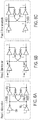
- FIGs. 6A-6C illustrate a sequence of how the circuit of FIG. 5A transitions from a 0 to a 1, in accordance with some embodiments.
- a 0 is provided as input to inverter 106 1 and a 1 is provided as input to inverter 106 3 .
- the output of inverter 106 1 is (1- ⁇ )VDD, where the value of ⁇ depends upon the voltages with which the header and footer transistors are biased.
- the outputs of inverters 106 2 and 106 4 are 0 and 1.
- the output of inverter 106 1 decreases and the output of inverter 106 3 increases.
- the slope with which these signals increase and decrease depends upon the time constants of the data paths.
- the output impedance of the feedback equalizers places parallel impedances at the outputs of inverters 106 1 and 106 3 , much like parallel resistor R 0 in FIG. 3B .
- the result is a reduction in the time constant of the lines.
- FIG. 7A is a block diagram illustrating a data path incorporating shunt devices and feedback equalizers, in accordance with some embodiments.
- the blocks labeled “Block IP,” “Block IN,” “Block 2P,” “Block 2N,” “Block 3P” and “Block 3N” may include inverters (see, e.g., inverters 106 of FIG. 4A or FIG. 5A ), buffers, amplifiers, or other suitable types of circuits.
- the blocks labeled "SH 1" and “SH 2” represent shunt devices, an example of which is shown in FIG. 4A .
- Shunt device SH 1 is disposed between the nodes V 1p and V 1n , and receives as input voltage V bSH1 .
- Shunt device SH 2 is disposed between the nodes V 2p and V 2n , and receives as input voltage V bSH2 .
- Voltage V BSH1 may represent, collectively, voltages V bp2 and V bn2 of FIG. 4A .
- voltage V bSH2 may represent, collectively, voltages V bp2 and V bn2 of FIG. 4A .
- the blocks labeled "FB IP,” “FB IN,” “FB 2P” and “FB 2N” represent feedback equalizers, examples of which are shown in FIG. 5A-5B .
- the feedback equalizers of the first stage receive voltage V bFB1 and the feedback equalizers of the second stage receive voltage V bFB2 .
- Voltage V bFB1 may represent, collectively, V bp and V bn of FIG. 5C .
- voltage V bFB2 may represent, collectively, V bp and V bn of FIG. 5C .
- FIG. 7B A specific implementation of the block diagram of FIG. 7A is illustrated in FIG. 7B , in accordance with some embodiments.
- the data path of FIG. 7B includes inverters 106, shunt devices having pairs of transistors 402 and 404, and feedback equalizers 502.
- Data paths of the types described herein may be implemented in a variety of contexts for transferring data from a source to a destination.
- FIG. 7C On specific context is depicted in FIG. 7C , and relates to the data path leading to a DAC.
- the multiplexers, the data paths and the DAC are part of a same chip labelled in FIG. 7C as a "TX" (transmitter).
- the transmitter is in communication with a receiver (“RX") via a communication channel (e.g., a trace on a printed circuit board, a wire or a cable).
- a communication channel e.g., a trace on a printed circuit board, a wire or a cable.
- the communication channel may be off-chip if the transmitter and the receiver are on separate chips, or on-chip if the transmitter and the receiver are on the same chip.
- the data paths may include shunt devices (as shown for example in FIG. 4A ), feedback equalizers (as shown for example in FIG. 5A ) or both (as shown for example in FIG. 7A ).
- FIG. 8 shows a comparison between the eye diagram of the circuit of FIG. 1A (800) and the circuit of FIG. 5A (801).
- the voltage rails are 0 and V DD
- the eye diagram 800 exhibits multiple trajectories that are substantially different from each other, resulting in a significant ISI.
- the trajectories of the eye diagram 801 match more closely, resulting in a significant reduction of the ISI.
- Coupled or “connected” is meant to refer to circuit elements, or signals, that are either directly linked to one another or through intermediate components.
- the terms “approximately”, “substantially,” and “about” may be used to mean within ⁇ 20% of a target value in some embodiments, within ⁇ 10% of a target value in some embodiments, within ⁇ 5% of a target value in some embodiments, and within ⁇ 2% of a target value in some embodiments.
- the terms “approximately” and “about” may include the target value.
Landscapes
- Engineering & Computer Science (AREA)
- Theoretical Computer Science (AREA)
- Computer Hardware Design (AREA)
- Physics & Mathematics (AREA)
- Computing Systems (AREA)
- General Engineering & Computer Science (AREA)
- Mathematical Physics (AREA)
- Power Engineering (AREA)
- Computer Networks & Wireless Communication (AREA)
- Signal Processing (AREA)
- Dc Digital Transmission (AREA)
- Logic Circuits (AREA)
Abstract
Description
- The present application relates to systems and methods for reducing pattern-dependent inter-symbol interference in electronic circuits.
- In telecommunications, inter-symbol interference (ISI) occurs when one symbol interferes with a subsequent or a previous symbol. This is an unwanted phenomenon as it leads to noise, thus making the communication less reliable. ISI is usually caused by multipath propagation or the inherent linear or non-linear frequency response of a communication channel causing successive symbols to mix together.
- Some embodiments relate to a system for reducing pattern-dependent inter-symbol interference (ISI). The system comprises a chip comprising a source including a multiplexer; a destination comprising an digital-to-analog converter (DAC); anda circuit disposed along a data path from the multiplexer to the DAC. The circuit is configured to receive a supply voltage; receive an input signal from the DAC, and produce an output signal based on the input signal, wherein producing the output signal comprises clamping the output signal to a voltage that is a fraction of the supply voltage.
- The circuit may be further configured to decrease a transition time of the output signal from a first value to the voltage by introducing a parallel resistance along the data path during at least a portion of the transition time.
- The source may be configured to transmit data to the destination at a data rate greater than 56Gb/s.
- The circuit may comprise a feedback equalizer.
- The feedback equalizer may comprise first and second open-loop buffers and first and second feedback buffers, the first feedback buffer being coupled between an input of the first open-loop buffer and an output of the second open-loop buffer and second feedback buffer being coupled between an input of the second open-loop buffer and an output of the first open-loop buffer.
- The first feedback buffer may comprise a header transistor, a footer transistor, and an inverter disposed between the header transistor and the footer transistor.
- The circuit may comprise a shunt device.
- The shunt device may comprise first and second buffers and one or more transistors connecting an output of the first buffer to an output of the second buffer.
- The circuit may comprise one or more complementary metal-oxide-semiconductor (CMOS) transistors.
- Some embodiments relate to a circuit disposed along a data path between a source to a destination The circuit comprises one or more complementary metal-oxide-semiconductor (CMOS) transistors. The circuit is configured to receive a supply voltage; receive an input signal from the source, and produce an output signal based on the input signal, wherein producing the output signal comprises clamping the output signal to a voltage that is a fraction of the supply voltage.
- The circuit may comprise a feedback equalizer comprising the one or more CMOS transistors.
- The feedback equalizer may comprise first and second open-loop buffers and first and second feedback buffers, the first feedback buffer being coupled between an input of the first open-loop buffer and an output of the second open-loop buffer and second feedback buffer being coupled between an input of the second open-loop buffer and an output of the first open-loop buffer.
- The first feedback buffer may comprise a header transistor, a footer transistor, and a CMOS inverter disposed between the header transistor and the footer transistor.
- The circuit may comprise a shunt device.
- The shunt device may comprise first and second buffers and the one or more CMOS transistors connect an output of the first buffer to an output of the second buffer.
- Some embodiments relate to a method comprising transmitting an input signal from a source to a destination with a data rate greater than 56Gb/s; and enabling transmission of the input signal from the source to the destination with a circuit disposed between the source and the destination. The enabling comprises receiving a supply voltage; receiving the input signal from the source ; and producing an output signal based on the input signal, wherein producing the output signal comprises clamping the output signal to a voltage that is a fraction of the supply voltage.
- The method may further comprise decreasing a transition time of the input signal from a first value to the voltage by introducing a parallel resistance along a data path positioned between the source and the destination during at least a portion of the transition time.
- Introducing a parallel resistance along the data path may comprise allowing a complementary metal-oxide-semiconductor (CMOS) inverter to transition from a first state to a second state.
- The fraction may be between 0.5 and 1.
- The source and the destination may be on a same chip.
- The foregoing summary is provided by way of illustration and is not intended to be limiting.
- The accompanying drawings are not intended to be drawn to scale. In the drawings, each identical or nearly identical component that is illustrated in various figures is represented by a like numeral. For purposes of clarity, not every component may be labeled in every drawing.
-
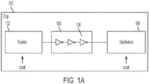
FIG. 1A is a block diagram illustrating an electronic communication link. -
FIG. 1B is a plot illustrating two example responses of the electronic communication link ofFIG. 1A . -
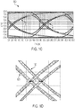
FIG. 1C is an eye diagram associated with the electronic communication link ofFIG. 1A . - FIG. ID illustrates a portion of the eye diagram of
FIG. 1C in additional detail. -
FIG. 2 is a plot illustrating a technique for reducing pattern-dependent inter-symbol interference, in accordance with some embodiments. -
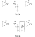
FIG. 3A is a circuit diagram illustrating a pair of inverters. -
FIG. 3B is a circuit diagram illustrating a pair of inverters and a parallel resistance, in accordance with some embodiments. -
FIG. 4A is a circuit diagram illustrating an example circuit for reducing pattern-dependent inter-symbol interference, in accordance with some embodiments. -
FIG. 4B is a circuit diagram illustrating an example of a bias circuit, in accordance with some embodiments. -
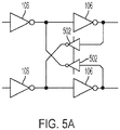
FIG. 5A is a circuit diagram illustrating another example circuit for reducing pattern-dependent inter-symbol interference, in accordance with some embodiments. -
FIG. 5B is a circuit diagram illustrating an example inverter that may be used in connection with the circuit ofFIG. 5A , in accordance with some embodiments. -
FIG. 5C is a circuit diagram illustrating another bias circuit, in accordance with some embodiments. -
FIGs. 6A-6C are circuit diagrams illustrating the circuit ofFIG. 6A as it transitions through different operational phases, in accordance with some embodiments. -
FIG. 7A is a block diagram illustrating a data path having shunt device and feedback equalizers, in accordance with some embodiments. -
FIG. 7B illustrates a specific implementation of the system ofFIG. 7B , in accordance with some embodiments. -
FIG. 7C illustrates a communication link having a transmitter and a receiver, in accordance with some embodiments. -
FIG. 8 is an eye diagram associated with the electronic communication system ofFIG. 5A . - New communication standards have emerged in the recent years which are expected to be deployed in cloud-based infrastructures including data centers. One such standard is the "112G," in which data are transferred at 112Gb/s, and which is expected to replace at least in some applications the "56G" standard. By increasing the speed at which data are transferred, these new communication standards will improve the overall capacity of the internet, and will be a key enabler of new applications such as the Internet-of-Things. Other standards operating at data rates greater than 56Gb/s (other than 112Gb/s) may emerge in the future.
- The inventors have appreciated, however, that increasing the speed at which data are transferred leads to a variety of drawbacks. One such drawback is pattern-dependent inter-symbol interference (ISI). Consider for example the chip of
FIG. 1A , which includes a source 102, adata path 103 and adestination 108. Source 102 is configured to transmit digital data todestination 108 with a high data rate, for example according to the 112G standard or according to any other standard with data rates in excess of 56Gb/s. - Source 102 may include various electronic circuits, including for example flip-flops, multiplexers and retimers, among other examples.
Destination 108 may include various electronic circuits, including for example flip-flops, multiplexers and digital-to-analog converters (DACs).Data path 103 may be a differential channel, in that it may include a pair of lines. Each line of the pair includesmultiple inverters 106, which are configured to facilitate transmission of the signal down the line. -
Data path 103 inevitably exhibits parasitics, such as parasitic capacitances and parasitic resistances, arising for example in the conductive traces and the inverters. At relatively low speeds, such as 56Gb/s or lower, the presence of these parasitics may affect the integrity of the signals propagating down the channel, but this effect is negligible, at least in some circumstances. At higher data rates, however, the impact of these parasitics on the integrity of the signals is more serious. In some circumstances, the degree to which the parasitics affect the signals may depend upon the signal pattern. - In
FIG. 1B , the bottom plot illustrates the response of the link ofFIG. 1A when the signal exhibits a slow pattern (in this case, 111000111000...) and the top plot illustrates the response when the signal exhibits a fast pattern (in this case, 10101010...). The terms "fast" and "slow" denote the frequency with which 1 and 0 alternate in a bit sequence. - Referring first to the top plot, signal 120 represents the waveform emerging from source 102, which toggles between the
voltage rails 0 and VDD. Signal 122 represents the waveform at some location downstream from source 102 alongdata path 103. Due to the presence of parasitics, the slope ofsignal 122 is not sufficiently high to permitsignal 122 to reach the voltage rails. Referring for example to the time interval between t1 and t2, signal 122 increases in response to signal 120 toggling from 0 to VDD. However, signal 120 toggles back to 0 beforesignal 122 has had sufficient time to reach VDD. This is because the parasitics of the communication channel increase the time constant at which signal 122 is able to vary over time, thereby reducing its slope. Similarly, signal 120 toggles back to VDD beforesignal 122 has had sufficient time to reach 0. The result is that the voltage rails ofsignal 122 are squeezed.Signal 122 swings between a value greater than 0 and a fraction of VDD. - Referring now to the bottom plot, signal 130 represents the waveform emerging from source 102, which toggles between the
voltage rails 0 and VDD. Signal 132 represents the waveform at some location downstream from source 102 alongcommunication channel 103. Due to the parasitics of communication channel, the slope ofsignal 132 is the same as the slope ofsignal 122. Unlikesignal 122, however, signal 132 does have sufficient time to reach thevoltage rails 0 and VDD. This is because the signal pattern is slower, meaning thatsignal 130 stays at the voltage rails for longer periods relative to signal 120. Thus, signal 132 swings between 0 and VDD. - Therefore, signals traveling down
communication channel 103 toggle between different values depending upon the pattern with which they are modulated. Patterns vary over time depending on the information being transmitted, meaning that the voltage rails of the traveling signals are continuously changing. The effect of this behavior is illustrated in the eye diagram ofFIG. 1C , a chart commonly used as an indicator of the quality of signals in high-speed digital transmissions. Eye diagrams are generated using oscilloscopes by overlaying sweeps of different segments of a long data stream. In an ideal world, eye diagrams have the shape of rectangular waveforms. In reality, the transitions do not line perfectly on top of each other, and an eye-shaped pattern results. -
Numeral 1320 represents the trajectory of signal 132 (associated with the slow pattern 111000111000...) and numeral 1220 represent the trajectory of signal 122 (associated with the fast pattern 10101010...). The vertical opening of the eye diagram is a qualitative measure of the integrity of the signal. Signal's 122 inability to reach thevoltage rails 0 and VDD results in an eye diagram that is partially closed. - Region R of the eye diagram is illustrated in FIG. ID in additional detail. As shown in FIG. ID, the signals associated with
numerals - The inventors have appreciated that pattern-dependent ISI-and as a result BER- in high data rate communication links can be reduced by clamping the signal traveling down the communication channel to a pair of voltage rails that are inside the voltage rails of the signal generated by the transmitter. In some embodiments, for example, the signal may be clamped to a voltage equal to (1-β)VDD and to a voltage equal to βVDD, where β is less than 1 (e.g., between 0.5 and 1). The value of β should be chosen, at least in some embodiments, so that the signal is able to reach the clamped voltage rails before toggling back to the previous value for any signal pattern.
- Consider for example the plot of
FIG. 2 , illustrating an example of how signal clamping may be performed, in accordance with some embodiments. Again, the top plot corresponds to a fast pattern 10101010... and the bottom plot corresponds to a slow pattern 111000111000... - Referring first to the top plot, signal 120 represents again the waveform emerging from source 102, which toggles between the
voltage rails 0 and VDD. Signal 122 represents the waveform at some location downstream from source 102 alongcommunication channel 103 absent the voltage clamping.Signal 126 represents the waveform at the same downstream location but when voltage clamping is applied. When signal 126 reaches (1-β)VDD, instead of continuing to increase as does signal 122, it remains clamped to (1-β)VDD until the subsequent falling edge. Similarly, whensignal 126 reaches βVDD, instead of continuing to decrease as does signal 122, it remains clamped to βVDD until the subsequent rising edge. - Referring now to the bottom plot, signal 130 represents again the waveform emerging from source 102, which toggles between the
voltage rails 0 and VDD. Signal 132 represents the waveform at some location downstream from source 102 alongdata path 103 absent the voltage clamping.Signal 136 represents the waveform at the same downstream location but when voltage clamping is applied. As in the previous case, signal 136 is clamped to (1-β)VDD before it can reach VDD, and is clamped to βVDD before it can reach 0. - The result is that the signal is clamped to the same voltage rails-βVDD and (1-β)VDD-regardless of the signal pattern. This is turn, reduces pattern-dependent ISI and BER.
- The inventors have appreciated that ISI may be further reduced by decreasing the time constant of the signal, thus increasing its slope and reducing the time with which the signal reaches the clamped voltage rail. Such a reduction in the time constant of the signal may be achieved by introducing a parallel resistance along the data path from source 102 to
destination 108.FIG. 3A is a circuit diagram illustrating a pair ofadjacent inverters 106 that are part of adata path 103. Resistance Rpar represents the parasitic resistance of the line and Cpar represents the parasitic capacitance of the line. In this example, the time constant with which the signal transitions from one value to another is given by the product of Rpar and Cpar (i.e., RparCpar). - In some embodiments, the time constant may be reduced by reducing this product, which may be achieved by reducing Rpar and/or Cpar. In the example of
FIG. 3B , a parallel resistance R0 is introduced along the line. Being placed in parallel, this resistance leads to a time constant of Cpar(R0 // Rpar) that is less than RparCpar. It should be appreciated that, in differential implementations, resistor R0 may be placed with one terminal coupled to one line of the pair and the other terminal coupled to the other line of the pair. - Notwithstanding the foregoing appreciation, the inventors have recognized that placing resistors along a data path may be impractical, as resistors are costly and difficult to implement in large scales.
- Recognizing this challenge, the inventors have developed circuits for introducing parallel resistances as shown in
FIG. 3B using complementary metal-oxide-semiconductor (CMOS) chips. CMOS chips of the types described herein are chips that include at least one p-MOS transistor and/or at least one n-MOS transistor. -
FIG. 4A is an example of such a circuit, in accordance with some embodiments. In this example,transistors transistor 402 is implemented as a p-MOS transistor andtransistor 404 is implemented as a n-MOS transistor. The drain of each transistor is coupled to the source of the other transistor. In some embodiments, the voltages with which the gates of the transistors are biased-Vbp2 and Vbn2-may be chosen to set the clamped voltage rail to a desired value. For example, the bias gate voltages may be chosen so that the clamped voltage rails are 0.2VDD and 0.8VDD, respectively. - The bias circuit of
FIG. 4B may be used to set Vbp2 and Vbn2. The bias circuit includes a pair of inverters that are substantially the same as the inverters ofFIG. 4A and a pair of transistors that are substantially the same astransistors FIG. 4A . In addition, the bias circuit includes a pair ofcomparators 410 having outputs in parallel with each other. The outputs of the comparators are provided at the gates oftransistors FIG. 4A , the outputs of the bias circuit are such that, if provided at the gates oftransistors FIG. 4A are clamped to 0.2VDD and 0.8VDD. - While
FIGs. 4A-4B illustrate inverters, non-inverting buffers may be used in other embodiments. -
FIG. 5A illustrates another circuit for reducing the time constant of the communication channel, in accordance with some embodiments. This circuit includes open-loop buffers (e.g., inverters) 106, andfeedback equalizers 502. Each feedback equalizer has an input coupled to a line of the differential pair and an output coupled to the other line of the differential pair, thus providing a feedback between the lines. - In some embodiments,
feedback equalizers 502 are implemented in the manner illustrated inFIG. 5B . In this example, a feedback equalizer includestransistors Transistors transistors Transistors Transistor 510 is a header transistor, in that it is coupled between the CMOS inverter and VDD. Transistor 516 is a footer transistor, in that it is coupled between the CMOS inverter and VSS (where in some embodiments, VSS=0). In some embodiments, the voltages with which the gates oftransistors - The bias circuit of
FIG. 5C may be used to set Vbp and Vbn. The bias circuit includes the same open-loop buffers and feedback equalizers as the circuit ofFIG. 5A , thereby mirroring its behavior. In some embodiments, the desired clamped voltage rails VREF_H and VREF_L are provided as inputs to one of the comparators. For instance, assuming that the user desires to set the clamped voltage rails to 0.2VDD and 0.8VDD, such voltages are provided as input to the comparator. Because the inverters and the transistors of the bias circuit mirror those of the circuit ofFIG. 5A , the outputs of the bias circuit are such that, if provided at the gates oftransistors FIG. 5A are clamped to 0.2VDD and 0.8VDD. In some embodiments, VL1 is different from VL2 and VH1 is different from VH2. In one specific example, VL1=0, VH1=VDD, VL2=βVDD and VH2=(1-βVDD), though other values are also possible. -
FIGs. 6A-6C illustrate a sequence of how the circuit ofFIG. 5A transitions from a 0 to a 1, in accordance with some embodiments. Initially, as shown inFIG. 6A , a 0 is provided as input toinverter 1061 and a 1 is provided as input toinverter 1063. The output ofinverter 1061 is (1-β)VDD, where the value of β depends upon the voltages with which the header and footer transistors are biased. The outputs ofinverters - As the inputs transition from 0 to 1 (upper line) and 1 to 0 (lower line), as shown in
FIG. 6B , the output ofinverter 1061 decreases and the output ofinverter 1063 increases. The slope with which these signals increase and decrease depends upon the time constants of the data paths. During the transitions, the output impedance of the feedback equalizers (see, e.g., terminal DIN ofFIG. 5B ) places parallel impedances at the outputs ofinverters FIG. 3B . As described above in connection withFIG. 3B , the result is a reduction in the time constant of the lines. - Finally, at
FIG. 6C , the circuit has completed the transition and the outputs ofinverters -
FIG. 7A is a block diagram illustrating a data path incorporating shunt devices and feedback equalizers, in accordance with some embodiments. The blocks labeled "Block IP," "Block IN," "Block 2P," "Block 2N," "Block 3P" and "Block 3N" may include inverters (see, e.g.,inverters 106 ofFIG. 4A orFIG. 5A ), buffers, amplifiers, or other suitable types of circuits. The blocks labeled "SH 1" and "SH 2" represent shunt devices, an example of which is shown inFIG. 4A .Shunt device SH 1 is disposed between the nodes V1p and V1n, and receives as input voltage VbSH1.Shunt device SH 2 is disposed between the nodes V2p and V2n, and receives as input voltage VbSH2. Voltage VBSH1 may represent, collectively, voltages Vbp2 and Vbn2 ofFIG. 4A . Similarly, voltage VbSH2 may represent, collectively, voltages Vbp2 and Vbn2 ofFIG. 4A . The blocks labeled "FB IP," "FB IN," "FB 2P" and "FB 2N" represent feedback equalizers, examples of which are shown inFIG. 5A-5B . The feedback equalizers of the first stage receive voltage VbFB1 and the feedback equalizers of the second stage receive voltage VbFB2. Voltage VbFB1 may represent, collectively, Vbp and Vbn ofFIG. 5C . Similarly, voltage VbFB2 may represent, collectively, Vbp and Vbn ofFIG. 5C . - A specific implementation of the block diagram of
FIG. 7A is illustrated inFIG. 7B , in accordance with some embodiments. The data path ofFIG. 7B includesinverters 106, shunt devices having pairs oftransistors feedback equalizers 502. - Data paths of the types described herein may be implemented in a variety of contexts for transferring data from a source to a destination. On specific context is depicted in
FIG. 7C , and relates to the data path leading to a DAC. In this example, the source includes multiplexers and the destination includes a n-bit DAC, where n=7 (though, n may have other values). The multiplexers, the data paths and the DAC are part of a same chip labelled inFIG. 7C as a "TX" (transmitter). The transmitter is in communication with a receiver ("RX") via a communication channel (e.g., a trace on a printed circuit board, a wire or a cable). The communication channel may be off-chip if the transmitter and the receiver are on separate chips, or on-chip if the transmitter and the receiver are on the same chip. The data paths may include shunt devices (as shown for example inFIG. 4A ), feedback equalizers (as shown for example inFIG. 5A ) or both (as shown for example inFIG. 7A ). -
FIG. 8 shows a comparison between the eye diagram of the circuit ofFIG. 1A (800) and the circuit ofFIG. 5A (801). In the eye diagram 800, the voltage rails are 0 and VDD, while in the eye diagram 801, the voltages are clamped to βVDD and (1-β)VDD, where β=0.14 in this example. For the reasons described above in connection with FIG. ID, the eye diagram 800 exhibits multiple trajectories that are substantially different from each other, resulting in a significant ISI. By contrast, the trajectories of the eye diagram 801 match more closely, resulting in a significant reduction of the ISI. - Use of ordinal terms such as "first", "second", "third", etc., in the claims to modify a claim element does not by itself connote any priority, precedence, or order of one claim element over another or the temporal order in which acts of a method are performed, but are used merely as labels to distinguish one claim element having a certain name from another element having a same name (but for use of the ordinal term) to distinguish the claim elements.
- Also, the phraseology and terminology used herein is for the purpose of description and should not be regarded as limiting. The use of "including", "comprising", "having", "containing" or "involving" and variations thereof herein, is meant to encompass the items listed thereafter and equivalents thereof as well as additional items.
- The use of "coupled" or "connected" is meant to refer to circuit elements, or signals, that are either directly linked to one another or through intermediate components.
- The terms "approximately", "substantially," and "about" may be used to mean within ±20% of a target value in some embodiments, within ±10% of a target value in some embodiments, within ±5% of a target value in some embodiments, and within ±2% of a target value in some embodiments. The terms "approximately" and "about" may include the target value.
Claims (15)
- A system for reducing pattern-dependent inter-symbol interference (ISI), the system comprising:
a chip comprising:a source including a multiplexer;a destination comprising an digital-to-analog converter (DAC); anda circuit disposed along a data path from the multiplexer to the DAC, the circuit being configured to:receive a supply voltage;receive an input signal from the DAC, andproduce an output signal based on the input signal, wherein producing the output signal comprises clamping the output signal to a voltage that is a fraction of the supply voltage. - The system of claim 1, wherein the circuit is further configured to decrease a transition time of the output signal from a first value to the voltage by introducing a parallel resistance along the data path during at least a portion of the transition time.
- The system of any preceding claim, wherein the source is configured to transmit data to the destination at a data rate greater than 56Gb/s.
- The system of any preceding claim, wherein the circuit comprises a feedback equalizer.
- The system of claim 4, wherein the feedback equalizer comprises first and second open-loop buffers and first and second feedback buffers, the first feedback buffer being coupled between an input of the first open-loop buffer and an output of the second open-loop buffer and second feedback buffer being coupled between an input of the second open-loop buffer and an output of the first open-loop buffer.
- The system of claim 5, wherein the first feedback buffer comprises a header transistor, a footer transistor, and an inverter disposed between the header transistor and the footer transistor.
- The system of any preceding claim, wherein the circuit comprises a shunt device.
- The system of claim 7, wherein the shunt device comprises first and second buffers and one or more transistors connecting an output of the first buffer to an output of the second buffer.
- The system of any preceding claim, wherein the circuit comprises one or more complementary metal-oxide-semiconductor (CMOS) transistors.
- A method comprising:transmitting an input signal from a source to a destination with a data rate greater than 56Gb/s; andenabling transmission of the input signal from the source to the destination with a circuit disposed between the source and the destination, wherein the enabling comprises:receiving a supply voltage;receiving the input signal from the source ; andproducing an output signal based on the input signal, wherein producing the output signal comprises clamping the output signal to a voltage that is a fraction of the supply voltage.
- The method of claim 10, further comprising decreasing a transition time of the input signal from a first value to the voltage by introducing a parallel resistance along a data path positioned between the source and the destination during at least a portion of the transition time.
- The method of any one of claims 10-11 , wherein introducing a parallel resistance along the data path comprises allowing a complementary metal-oxide-semiconductor (CMOS) inverter to transition from a first state to a second state.
- The method of any one of claims 10-12, wherein the fraction is between 0.5 and 1.
- The method of any one of claims 10-13 , wherein the source and the destination are on a same chip.
- The method of any one of claims 10-14, wherein introducing a parallel resistance along the data path comprises activating a shunt device.
Applications Claiming Priority (2)
| Application Number | Priority Date | Filing Date | Title |
|---|---|---|---|
| US201962796204P | 2019-01-24 | 2019-01-24 | |
| US16/579,456 US10804924B2 (en) | 2019-01-24 | 2019-09-23 | Systems for reducing pattern-dependent inter-symbol interference and related methods |
Publications (2)
| Publication Number | Publication Date |
|---|---|
| EP3687127A1 true EP3687127A1 (en) | 2020-07-29 |
| EP3687127B1 EP3687127B1 (en) | 2022-05-11 |
Family
ID=69147546
Family Applications (1)
| Application Number | Title | Priority Date | Filing Date |
|---|---|---|---|
| EP20150708.4A Active EP3687127B1 (en) | 2019-01-24 | 2020-01-08 | Systems for reducing pattern-dependent inter-symbol interference and related methods |
Country Status (4)
| Country | Link |
|---|---|
| US (1) | US10804924B2 (en) |
| EP (1) | EP3687127B1 (en) |
| CN (1) | CN111478701B (en) |
| TW (1) | TWI710219B (en) |
Citations (4)
| Publication number | Priority date | Publication date | Assignee | Title |
|---|---|---|---|---|
| GB2381882A (en) * | 2001-11-09 | 2003-05-14 | Micron Technology Inc | Voltage clamp circuit |
| US20060244479A1 (en) * | 2005-04-27 | 2006-11-02 | Broadcom Corporation | Driver circuit having programmable slew rate |
| US7148725B1 (en) * | 2004-06-04 | 2006-12-12 | Intel Corporation | Voltage clamp |
| US20120146686A1 (en) * | 2010-12-14 | 2012-06-14 | Qualcomm Incorporated | Pre-emphasis technique for on-chip voltage-driven single-ended-termination drivers |
Family Cites Families (5)
| Publication number | Priority date | Publication date | Assignee | Title |
|---|---|---|---|---|
| US6247138B1 (en) | 1997-06-12 | 2001-06-12 | Fujitsu Limited | Timing signal generating circuit, semiconductor integrated circuit device and semiconductor integrated circuit system to which the timing signal generating circuit is applied, and signal transmission system |
| US6388495B1 (en) * | 2001-02-23 | 2002-05-14 | Sun Microsystems, Inc. | Dynamic termination and clamping circuit |
| CN101674073A (en) | 2009-06-09 | 2010-03-17 | 中国人民解放军国防科学技术大学 | Self-adapting amplitude-limiting output intersymbol interference suppression circuit for differential voltage signal with low oscillation amplitude |
| US8547140B1 (en) | 2010-11-03 | 2013-10-01 | Pmc-Sierra, Inc. | Apparatus and method for generating a bias voltage |
| US10187230B1 (en) * | 2017-09-08 | 2019-01-22 | Inphi Corporation | Equalization for transmitter input buffer array |
-
2019
- 2019-09-23 US US16/579,456 patent/US10804924B2/en active Active
- 2019-11-26 CN CN201911174369.3A patent/CN111478701B/en active Active
- 2019-11-28 TW TW108143312A patent/TWI710219B/en active
-
2020
- 2020-01-08 EP EP20150708.4A patent/EP3687127B1/en active Active
Patent Citations (4)
| Publication number | Priority date | Publication date | Assignee | Title |
|---|---|---|---|---|
| GB2381882A (en) * | 2001-11-09 | 2003-05-14 | Micron Technology Inc | Voltage clamp circuit |
| US7148725B1 (en) * | 2004-06-04 | 2006-12-12 | Intel Corporation | Voltage clamp |
| US20060244479A1 (en) * | 2005-04-27 | 2006-11-02 | Broadcom Corporation | Driver circuit having programmable slew rate |
| US20120146686A1 (en) * | 2010-12-14 | 2012-06-14 | Qualcomm Incorporated | Pre-emphasis technique for on-chip voltage-driven single-ended-termination drivers |
Non-Patent Citations (1)
| Title |
|---|
| MARSHNIL DAVE ET AL: "A Variation Tolerant Current-Mode Signaling Scheme for On-Chip Interconnects", IEEE TRANSACTIONS ON VERY LARGE SCALE INTEGRATION (VLSI) SYSTEMS, IEEE SERVICE CENTER, PISCATAWAY, NJ, USA, vol. 21, no. 2, 1 February 2013 (2013-02-01), pages 342 - 353, XP011488657, ISSN: 1063-8210, DOI: 10.1109/TVLSI.2012.2185835 * |
Also Published As
| Publication number | Publication date |
|---|---|
| TW202029653A (en) | 2020-08-01 |
| CN111478701A (en) | 2020-07-31 |
| TWI710219B (en) | 2020-11-11 |
| US10804924B2 (en) | 2020-10-13 |
| EP3687127B1 (en) | 2022-05-11 |
| US20200244280A1 (en) | 2020-07-30 |
| CN111478701B (en) | 2023-08-04 |
Similar Documents
| Publication | Publication Date | Title |
|---|---|---|
| CN111061664B (en) | Two-stage feed-forward equalizer for voltage modal signal transmitter | |
| US6977534B2 (en) | Low voltage differential signaling [LVDS] driver with pre-emphasis | |
| US7307447B2 (en) | Self series terminated serial link transmitter having segmentation for amplitude, pre-emphasis, and slew rate control and voltage regulation for amplitude accuracy and high voltage protection | |
| US8258813B2 (en) | Circuit and method for driving at least one differential line | |
| US20070057702A1 (en) | Output buffer circuit | |
| US20090190648A1 (en) | Differential transmitter | |
| JP2018125796A (en) | PAM receiving circuit and receiving apparatus | |
| WO2016134606A1 (en) | Transmitter apparatus and method | |
| Grozing et al. | Sampling receive equalizer with bit-rate flexible operation up to 10 Gbit/s | |
| US20120146686A1 (en) | Pre-emphasis technique for on-chip voltage-driven single-ended-termination drivers | |
| JP2005109897A (en) | Lvds driver circuit | |
| US20120032656A1 (en) | Voltage regulator for impedance matching and pre-emphasis, method of regulating voltage for impedance matching and pre-emphasis, voltage mode driver including the voltage regulator, and voltage-mode driver using the method | |
| US7920014B2 (en) | Semiconductor integrated circuit device | |
| US11223378B2 (en) | Semiconductor integrated circuit, transmission device, and control method of transmission device | |
| US10804924B2 (en) | Systems for reducing pattern-dependent inter-symbol interference and related methods | |
| JP5076391B2 (en) | Differential signal transmission system and signal line skew adjustment method | |
| EP1050138B1 (en) | Cmos driver and on-chip termination for gigabaud speed data communication | |
| Forghani et al. | Circuit bandwidth requirements for NRZ and PAM4 signals | |
| US20240421807A1 (en) | Semiconductor integrated circuit and receiver device | |
| US8068537B2 (en) | Communication circuit for a bi-directional data transmission | |
| KR102203394B1 (en) | Decision feedback equalizer circuit for pulse amplitude modulation 4 and operation method thereof | |
| Hu et al. | An R2R-DAC-based architecture for equalization-equipped voltage-mode PAM-4 wireline transmitter design | |
| US7440494B2 (en) | Method and system of bidirectional data transmission and reception | |
| JP2024131178A (en) | Semiconductor integrated circuit and receiving device | |
| US20090128119A1 (en) | Differential output circuit |
Legal Events
| Date | Code | Title | Description |
|---|---|---|---|
| PUAI | Public reference made under article 153(3) epc to a published international application that has entered the european phase |
Free format text: ORIGINAL CODE: 0009012 |
|
| STAA | Information on the status of an ep patent application or granted ep patent |
Free format text: STATUS: THE APPLICATION HAS BEEN PUBLISHED |
|
| AK | Designated contracting states |
Kind code of ref document: A1 Designated state(s): AL AT BE BG CH CY CZ DE DK EE ES FI FR GB GR HR HU IE IS IT LI LT LU LV MC MK MT NL NO PL PT RO RS SE SI SK SM TR |
|
| AX | Request for extension of the european patent |
Extension state: BA ME |
|
| STAA | Information on the status of an ep patent application or granted ep patent |
Free format text: STATUS: REQUEST FOR EXAMINATION WAS MADE |
|
| 17P | Request for examination filed |
Effective date: 20210126 |
|
| RBV | Designated contracting states (corrected) |
Designated state(s): AL AT BE BG CH CY CZ DE DK EE ES FI FR GB GR HR HU IE IS IT LI LT LU LV MC MK MT NL NO PL PT RO RS SE SI SK SM TR |
|
| GRAP | Despatch of communication of intention to grant a patent |
Free format text: ORIGINAL CODE: EPIDOSNIGR1 |
|
| STAA | Information on the status of an ep patent application or granted ep patent |
Free format text: STATUS: GRANT OF PATENT IS INTENDED |
|
| INTG | Intention to grant announced |
Effective date: 20211208 |
|
| GRAS | Grant fee paid |
Free format text: ORIGINAL CODE: EPIDOSNIGR3 |
|
| GRAA | (expected) grant |
Free format text: ORIGINAL CODE: 0009210 |
|
| STAA | Information on the status of an ep patent application or granted ep patent |
Free format text: STATUS: THE PATENT HAS BEEN GRANTED |
|
| AK | Designated contracting states |
Kind code of ref document: B1 Designated state(s): AL AT BE BG CH CY CZ DE DK EE ES FI FR GB GR HR HU IE IS IT LI LT LU LV MC MK MT NL NO PL PT RO RS SE SI SK SM TR |
|
| REG | Reference to a national code |
Ref country code: GB Ref legal event code: FG4D |
|
| REG | Reference to a national code |
Ref country code: CH Ref legal event code: EP |
|
| REG | Reference to a national code |
Ref country code: AT Ref legal event code: REF Ref document number: 1492454 Country of ref document: AT Kind code of ref document: T Effective date: 20220515 |
|
| REG | Reference to a national code |
Ref country code: DE Ref legal event code: R096 Ref document number: 602020003066 Country of ref document: DE |
|
| REG | Reference to a national code |
Ref country code: IE Ref legal event code: FG4D |
|
| REG | Reference to a national code |
Ref country code: LT Ref legal event code: MG9D |
|
| REG | Reference to a national code |
Ref country code: NL Ref legal event code: MP Effective date: 20220511 |
|
| REG | Reference to a national code |
Ref country code: AT Ref legal event code: MK05 Ref document number: 1492454 Country of ref document: AT Kind code of ref document: T Effective date: 20220511 |
|
| PG25 | Lapsed in a contracting state [announced via postgrant information from national office to epo] |
Ref country code: SE Free format text: LAPSE BECAUSE OF FAILURE TO SUBMIT A TRANSLATION OF THE DESCRIPTION OR TO PAY THE FEE WITHIN THE PRESCRIBED TIME-LIMIT Effective date: 20220511 Ref country code: PT Free format text: LAPSE BECAUSE OF FAILURE TO SUBMIT A TRANSLATION OF THE DESCRIPTION OR TO PAY THE FEE WITHIN THE PRESCRIBED TIME-LIMIT Effective date: 20220912 Ref country code: NO Free format text: LAPSE BECAUSE OF FAILURE TO SUBMIT A TRANSLATION OF THE DESCRIPTION OR TO PAY THE FEE WITHIN THE PRESCRIBED TIME-LIMIT Effective date: 20220811 Ref country code: NL Free format text: LAPSE BECAUSE OF FAILURE TO SUBMIT A TRANSLATION OF THE DESCRIPTION OR TO PAY THE FEE WITHIN THE PRESCRIBED TIME-LIMIT Effective date: 20220511 Ref country code: LT Free format text: LAPSE BECAUSE OF FAILURE TO SUBMIT A TRANSLATION OF THE DESCRIPTION OR TO PAY THE FEE WITHIN THE PRESCRIBED TIME-LIMIT Effective date: 20220511 Ref country code: HR Free format text: LAPSE BECAUSE OF FAILURE TO SUBMIT A TRANSLATION OF THE DESCRIPTION OR TO PAY THE FEE WITHIN THE PRESCRIBED TIME-LIMIT Effective date: 20220511 Ref country code: GR Free format text: LAPSE BECAUSE OF FAILURE TO SUBMIT A TRANSLATION OF THE DESCRIPTION OR TO PAY THE FEE WITHIN THE PRESCRIBED TIME-LIMIT Effective date: 20220812 Ref country code: FI Free format text: LAPSE BECAUSE OF FAILURE TO SUBMIT A TRANSLATION OF THE DESCRIPTION OR TO PAY THE FEE WITHIN THE PRESCRIBED TIME-LIMIT Effective date: 20220511 Ref country code: ES Free format text: LAPSE BECAUSE OF FAILURE TO SUBMIT A TRANSLATION OF THE DESCRIPTION OR TO PAY THE FEE WITHIN THE PRESCRIBED TIME-LIMIT Effective date: 20220511 Ref country code: BG Free format text: LAPSE BECAUSE OF FAILURE TO SUBMIT A TRANSLATION OF THE DESCRIPTION OR TO PAY THE FEE WITHIN THE PRESCRIBED TIME-LIMIT Effective date: 20220811 Ref country code: AT Free format text: LAPSE BECAUSE OF FAILURE TO SUBMIT A TRANSLATION OF THE DESCRIPTION OR TO PAY THE FEE WITHIN THE PRESCRIBED TIME-LIMIT Effective date: 20220511 |
|
| PG25 | Lapsed in a contracting state [announced via postgrant information from national office to epo] |
Ref country code: RS Free format text: LAPSE BECAUSE OF FAILURE TO SUBMIT A TRANSLATION OF THE DESCRIPTION OR TO PAY THE FEE WITHIN THE PRESCRIBED TIME-LIMIT Effective date: 20220511 Ref country code: PL Free format text: LAPSE BECAUSE OF FAILURE TO SUBMIT A TRANSLATION OF THE DESCRIPTION OR TO PAY THE FEE WITHIN THE PRESCRIBED TIME-LIMIT Effective date: 20220511 Ref country code: LV Free format text: LAPSE BECAUSE OF FAILURE TO SUBMIT A TRANSLATION OF THE DESCRIPTION OR TO PAY THE FEE WITHIN THE PRESCRIBED TIME-LIMIT Effective date: 20220511 Ref country code: IS Free format text: LAPSE BECAUSE OF FAILURE TO SUBMIT A TRANSLATION OF THE DESCRIPTION OR TO PAY THE FEE WITHIN THE PRESCRIBED TIME-LIMIT Effective date: 20220911 |
|
| PG25 | Lapsed in a contracting state [announced via postgrant information from national office to epo] |
Ref country code: SM Free format text: LAPSE BECAUSE OF FAILURE TO SUBMIT A TRANSLATION OF THE DESCRIPTION OR TO PAY THE FEE WITHIN THE PRESCRIBED TIME-LIMIT Effective date: 20220511 Ref country code: SK Free format text: LAPSE BECAUSE OF FAILURE TO SUBMIT A TRANSLATION OF THE DESCRIPTION OR TO PAY THE FEE WITHIN THE PRESCRIBED TIME-LIMIT Effective date: 20220511 Ref country code: RO Free format text: LAPSE BECAUSE OF FAILURE TO SUBMIT A TRANSLATION OF THE DESCRIPTION OR TO PAY THE FEE WITHIN THE PRESCRIBED TIME-LIMIT Effective date: 20220511 Ref country code: EE Free format text: LAPSE BECAUSE OF FAILURE TO SUBMIT A TRANSLATION OF THE DESCRIPTION OR TO PAY THE FEE WITHIN THE PRESCRIBED TIME-LIMIT Effective date: 20220511 Ref country code: DK Free format text: LAPSE BECAUSE OF FAILURE TO SUBMIT A TRANSLATION OF THE DESCRIPTION OR TO PAY THE FEE WITHIN THE PRESCRIBED TIME-LIMIT Effective date: 20220511 Ref country code: CZ Free format text: LAPSE BECAUSE OF FAILURE TO SUBMIT A TRANSLATION OF THE DESCRIPTION OR TO PAY THE FEE WITHIN THE PRESCRIBED TIME-LIMIT Effective date: 20220511 |
|
| REG | Reference to a national code |
Ref country code: DE Ref legal event code: R097 Ref document number: 602020003066 Country of ref document: DE |
|
| PLBE | No opposition filed within time limit |
Free format text: ORIGINAL CODE: 0009261 |
|
| STAA | Information on the status of an ep patent application or granted ep patent |
Free format text: STATUS: NO OPPOSITION FILED WITHIN TIME LIMIT |
|
| PG25 | Lapsed in a contracting state [announced via postgrant information from national office to epo] |
Ref country code: AL Free format text: LAPSE BECAUSE OF FAILURE TO SUBMIT A TRANSLATION OF THE DESCRIPTION OR TO PAY THE FEE WITHIN THE PRESCRIBED TIME-LIMIT Effective date: 20220511 |
|
| 26N | No opposition filed |
Effective date: 20230214 |
|
| PG25 | Lapsed in a contracting state [announced via postgrant information from national office to epo] |
Ref country code: SI Free format text: LAPSE BECAUSE OF FAILURE TO SUBMIT A TRANSLATION OF THE DESCRIPTION OR TO PAY THE FEE WITHIN THE PRESCRIBED TIME-LIMIT Effective date: 20220511 |
|
| P01 | Opt-out of the competence of the unified patent court (upc) registered |
Effective date: 20230627 |
|
| REG | Reference to a national code |
Ref country code: CH Ref legal event code: PL |
|
| PG25 | Lapsed in a contracting state [announced via postgrant information from national office to epo] |
Ref country code: LU Free format text: LAPSE BECAUSE OF NON-PAYMENT OF DUE FEES Effective date: 20230108 |
|
| REG | Reference to a national code |
Ref country code: BE Ref legal event code: MM Effective date: 20230131 |
|
| PG25 | Lapsed in a contracting state [announced via postgrant information from national office to epo] |
Ref country code: LI Free format text: LAPSE BECAUSE OF NON-PAYMENT OF DUE FEES Effective date: 20230131 Ref country code: CH Free format text: LAPSE BECAUSE OF NON-PAYMENT OF DUE FEES Effective date: 20230131 |
|
| PG25 | Lapsed in a contracting state [announced via postgrant information from national office to epo] |
Ref country code: BE Free format text: LAPSE BECAUSE OF NON-PAYMENT OF DUE FEES Effective date: 20230131 |
|
| PG25 | Lapsed in a contracting state [announced via postgrant information from national office to epo] |
Ref country code: IT Free format text: LAPSE BECAUSE OF FAILURE TO SUBMIT A TRANSLATION OF THE DESCRIPTION OR TO PAY THE FEE WITHIN THE PRESCRIBED TIME-LIMIT Effective date: 20220511 Ref country code: IE Free format text: LAPSE BECAUSE OF NON-PAYMENT OF DUE FEES Effective date: 20230108 |
|
| PG25 | Lapsed in a contracting state [announced via postgrant information from national office to epo] |
Ref country code: MC Free format text: LAPSE BECAUSE OF FAILURE TO SUBMIT A TRANSLATION OF THE DESCRIPTION OR TO PAY THE FEE WITHIN THE PRESCRIBED TIME-LIMIT Effective date: 20220511 |
|
| PG25 | Lapsed in a contracting state [announced via postgrant information from national office to epo] |
Ref country code: MC Free format text: LAPSE BECAUSE OF FAILURE TO SUBMIT A TRANSLATION OF THE DESCRIPTION OR TO PAY THE FEE WITHIN THE PRESCRIBED TIME-LIMIT Effective date: 20220511 |
|
| PG25 | Lapsed in a contracting state [announced via postgrant information from national office to epo] |
Ref country code: BG Free format text: LAPSE BECAUSE OF FAILURE TO SUBMIT A TRANSLATION OF THE DESCRIPTION OR TO PAY THE FEE WITHIN THE PRESCRIBED TIME-LIMIT Effective date: 20220511 |
|
| PG25 | Lapsed in a contracting state [announced via postgrant information from national office to epo] |
Ref country code: BG Free format text: LAPSE BECAUSE OF FAILURE TO SUBMIT A TRANSLATION OF THE DESCRIPTION OR TO PAY THE FEE WITHIN THE PRESCRIBED TIME-LIMIT Effective date: 20220511 |
|
| PG25 | Lapsed in a contracting state [announced via postgrant information from national office to epo] |
Ref country code: CY Free format text: LAPSE BECAUSE OF FAILURE TO SUBMIT A TRANSLATION OF THE DESCRIPTION OR TO PAY THE FEE WITHIN THE PRESCRIBED TIME-LIMIT; INVALID AB INITIO Effective date: 20200108 |
|
| PG25 | Lapsed in a contracting state [announced via postgrant information from national office to epo] |
Ref country code: HU Free format text: LAPSE BECAUSE OF FAILURE TO SUBMIT A TRANSLATION OF THE DESCRIPTION OR TO PAY THE FEE WITHIN THE PRESCRIBED TIME-LIMIT; INVALID AB INITIO Effective date: 20200108 |
|
| PG25 | Lapsed in a contracting state [announced via postgrant information from national office to epo] |
Ref country code: TR Free format text: LAPSE BECAUSE OF FAILURE TO SUBMIT A TRANSLATION OF THE DESCRIPTION OR TO PAY THE FEE WITHIN THE PRESCRIBED TIME-LIMIT Effective date: 20220511 |
|
| PGFP | Annual fee paid to national office [announced via postgrant information from national office to epo] |
Ref country code: GB Payment date: 20251120 Year of fee payment: 7 |
|
| PGFP | Annual fee paid to national office [announced via postgrant information from national office to epo] |
Ref country code: FR Payment date: 20251110 Year of fee payment: 7 |
|
| PGFP | Annual fee paid to national office [announced via postgrant information from national office to epo] |
Ref country code: DE Payment date: 20251111 Year of fee payment: 7 |