EP3687068A1 - A method of driving a capacitive load, corresponding circuit and device - Google Patents
A method of driving a capacitive load, corresponding circuit and device Download PDFInfo
- Publication number
- EP3687068A1 EP3687068A1 EP20151638.2A EP20151638A EP3687068A1 EP 3687068 A1 EP3687068 A1 EP 3687068A1 EP 20151638 A EP20151638 A EP 20151638A EP 3687068 A1 EP3687068 A1 EP 3687068A1
- Authority
- EP
- European Patent Office
- Prior art keywords
- charge
- transistor
- node
- capacitance
- load
- Prior art date
- Legal status (The legal status is an assumption and is not a legal conclusion. Google has not performed a legal analysis and makes no representation as to the accuracy of the status listed.)
- Granted
Links
Images



Classifications
-
- H—ELECTRICITY
- H03—ELECTRONIC CIRCUITRY
- H03K—PULSE TECHNIQUE
- H03K17/00—Electronic switching or gating, i.e. not by contact-making and –breaking
- H03K17/51—Electronic switching or gating, i.e. not by contact-making and –breaking characterised by the components used
- H03K17/56—Electronic switching or gating, i.e. not by contact-making and –breaking characterised by the components used by the use, as active elements, of semiconductor devices
- H03K17/687—Electronic switching or gating, i.e. not by contact-making and –breaking characterised by the components used by the use, as active elements, of semiconductor devices the devices being field-effect transistors
- H03K17/6871—Electronic switching or gating, i.e. not by contact-making and –breaking characterised by the components used by the use, as active elements, of semiconductor devices the devices being field-effect transistors the output circuit comprising more than one controlled field-effect transistor
- H03K17/6874—Electronic switching or gating, i.e. not by contact-making and –breaking characterised by the components used by the use, as active elements, of semiconductor devices the devices being field-effect transistors the output circuit comprising more than one controlled field-effect transistor in a symmetrical configuration
-
- H—ELECTRICITY
- H03—ELECTRONIC CIRCUITRY
- H03K—PULSE TECHNIQUE
- H03K4/00—Generating pulses having essentially a finite slope or stepped portions
- H03K4/02—Generating pulses having essentially a finite slope or stepped portions having stepped portions, e.g. staircase waveform
- H03K4/023—Generating pulses having essentially a finite slope or stepped portions having stepped portions, e.g. staircase waveform by repetitive charge or discharge of a capacitor, analogue generators
-
- H—ELECTRICITY
- H10—SEMICONDUCTOR DEVICES; ELECTRIC SOLID-STATE DEVICES NOT OTHERWISE PROVIDED FOR
- H10N—ELECTRIC SOLID-STATE DEVICES NOT OTHERWISE PROVIDED FOR
- H10N30/00—Piezoelectric or electrostrictive devices
- H10N30/80—Constructional details
- H10N30/802—Circuitry or processes for operating piezoelectric or electrostrictive devices not otherwise provided for, e.g. drive circuits
Definitions
- the description relates to driving capacitive loads.
- Piezoelectric loads such as micro-mirrors may be exemplary of capacitive loads to which embodiments may apply.
- One or more embodiments may be applied to so-called charge reuse drivers including electronic switches, for instance high voltage and low resistance switches with fast and efficient turn-on time.
- a load e.g. a capacitance
- Such a signal may result from a stepped exchange of charge (and/or high voltage VHV) between a load capacitance and storage "tank" capacitances, the exchange comprising a set of intermediate sub-steps.
- a tank capacitance may store a respective intermediate voltage, e.g. an n-th fraction of the voltage VHV.
- the load capacitance itself may be charged or discharged (e.g., depending on whether it is performed during the rising or falling edge of the periodic signal, respectively) through the tank capacitors.
- the amount of charge gained from the load capacitance during the rising edge may be (asymptotically) equal to the amount of charge lost during the falling edge.
- the load capacitance may, e.g. continuously, exchange charge with the tank capacitors.
- Charge reuse drivers may be adopted in low-voltage applications. Applying such drivers also to piezoelectric loads, e.g. to resonant micro-mirrors may be desirable.
- micro-mirrors may have intrinsic capacitances of several nanoFarads and resonance frequencies up tens of kiloHertz.
- Power dissipation may thus a figure of merit deserving consideration.
- An object of one or more embodiments is to contribute in addressing the aspects discussed above.
- One or more embodiments may relate to a corresponding circuit.
- One or more embodiments may relate to a corresponding device.
- a device comprising a charge reuse driver and a piezoelectric load (e.g. a micro-mirror) driven thereby may be exemplary of such a system.
- improved performance may be facilitated in a charge reuse driver via an increasing number of sub-steps N.
- time devoted to rise/fall edges may be reduced (i.e. increasing the resonance frequency).
- switching operation may use short switch turn-on times (so that rise/fall times are not appreciably affected) and (very) low switch resistance.
- One or more embodiments may involve a high-voltage switch with low resistance and (very) low turn-on times.
- high-voltage switch devices may facilitate transferring voltages up to 40V between load and tank (or storage) capacitances, in either direction.
- One or more embodiments may adopt efficient driving circuits with well controlled safe operation area (SOA) constraints.
- SOA safe operation area
- one or more embodiments may be based on the recognition that the turn-on transient time and the final DC resistance in a conventional switch circuit may be limited by a limited on-set resistance r ON , by non-negligible parasitic capacitances and by SOA constraints.
- One or more embodiments may comprise charge reuse drivers suitable for use in high voltage applications, in which a capacitive load being driven through a period signal.
- each sub-step in the set of steps of the charge reuse driver e.g. each tank capacitance
- each sub-step in the set of steps of the charge reuse driver complete its transient phase - either charging or discharging the RC circuit - e.g. with 4 to 5 RC time constants may facilitate benefitting from power consumption reduction.
- reducing rise and fall times may be desirable in order to improve the power efficiency in applying the driving signal to the load.
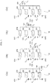
- FIG. 1 is exemplary of working principles of a charge reuse driver 10, e.g. which, as exemplified herein, may be used to drive a capacitive load C L , e.g. a piezoelectric actuator such as a micro-mirror.
- a charge reuse driver 10 e.g. which, as exemplified herein, may be used to drive a capacitive load C L , e.g. a piezoelectric actuator such as a micro-mirror.
- the charge reuse driver 10 may comprise a number N of sub-stages in which charge may be redistributed sequentially between the capacitive load C L and the N sub-stages.
- the charge reuse driver 10 may comprise a set of N switches 200, 201, 202, 20N, e.g. four switches 200, 201, 202, 20N.
- the number N of sub-stages in the charge reuse driver 10 may comprise:
- switches in the set of N switches 200, 201, 202, 20N may be configured to drive the charge node 104 of the capacitive load C L by applying thereto a sequence of rising and falling edges of a voltage signal.
- providing such rising and falling edges may comprise performing stages of an ordered sequence, shown in respective portions 10a), 10b), 10c), 10d) of Figure 1 .
- a controller may operate the reusable charge driver 10 to perform the sequence as exemplified in Figure 1 .
- the number of tank capacitances may be equal to N-2 where N is the number of sub-steps.
- Portions 10a) to 10d) of Figure 1 are exemplary of producing across the load capacitance C L a "trapezoidal" voltage signal having rising edges (from ground GND to VHV) and falling edges (form VHV to ground GND).
- a "rightward" sequence from 10a) to 10d) is exemplary of a rising edge while a “leftward” sequence from 10d) to 10a) is exemplary of a falling edge.
- Providing a rising edge may comprise coupling the charge node of the load capacitance as exemplified in Figure 1 going from 10a) to 10d).
- the charge reuse driver 10 may close (e.g. turning on) solely the first switch 200, while maintaining open the remaining switches 201, 202, 20N in the set of switches (e.g. turned off). Accordingly, in the first stage as exemplified in portion 10a) of Figure 1 , the load capacitance C L may be coupled to the ground node GND, e.g. maintaining the load capacitance C L discharged.
- the charge reuse driver 10 may close (e.g. turning on) solely the second switch 201, while maintaining open the remaining switches 200, 202, 20N in the set of switches (e.g. turned off). Accordingly, in the second stage as exemplified in portion 10b) of Figure 1 , the charge node 101 first storage capacitance C 1 may be coupled to the charge node 104 of the load capacitance C L .
- tank capacitances C 1 , C 2 may have higher capacitance values than capacitance values of the load C L to be driven, e.g. C 1 >>C L , C 2 >>C L .
- a charge redistribution process may start.
- the tank capacitance C 1 may have a bigger value than the load capacitance C L , the voltage drop across the load V L may reach approximately the same value of the voltage drop across the respective tank capacitance C 1 .
- the load capacitance C L may partially receive charge from or give charge to the tank capacitance C 1 as a function of whether coupling is performed while in the rising or falling edge of the ordered sequence, respectively.
- voltage across the tank capacitance C 1 may be treated as unvaried, e.g. having a like value as a result of the process asymptotically tending to an exchange of similar charge quantities in periodic operation of the driver and of mentioned capacitances ratios C 1 /C L >>1.
- the charge reuse driver 10 may close (e.g. turning on) solely the third switch 202, while maintaining open the remaining switches 200, 201, 20N in the set of switches (e.g. turned off). Accordingly, in the third stage as exemplified in portion 10c) of Figure 1 , the charge node 102 of the second storage capacitance C 2 may be coupled to the charge node 104 of the load capacitance C L .
- the charge reuse driver 10 may close (e.g. turning on) solely the fourth switch 20N, while maintaining open the remaining switches 200, 201, 202 in the set of switches (e.g. turned off).
- the voltage supply node VHV may be coupled to the charge node 104 of the load capacitance C L . Consequently, a process of charging the load capacitance C L may begin.
- sequence stages 10a), 10b), 10c), 10d) may be performed in a different order with respect to the order discussed in the foregoing, e.g. beginning with the load capacitor C L charged up and moving "backwards" from phase 10d) to phase 10a).
- the sequence may be self-sustaining, performing operations periodically oscillating from the first stage 10a) to the fourth stage 10d and from the fourth stage 10d) to first stage 10a).
- the periodic driving sequence may reach a "stationary" condition for what concern the charge stored into the tank capacitors. For instance, at one sub-step on the falling edge the charge "lost" in the previous rising edge period may be “recovered”.
- a stationary condition may be reached in which tank capacitances have a "constant" (e.g. neglecting second order effects, leakage or charge injections resulting from switching) voltage across.
- a stationary condition may result from operating the charge reuse so that: at an i-th step, the load capacitance C L receives a discrete charge quantity from a respective tank capacitance C 1 , and at the j-th step, where j is a step involving a same tank capacitance C1 but on the opposite falling edge of the previous i-th step, e.g.
- the tank C1 receives from the load C L a same discrete charge quantity to the one that was earlier (at i-th stage) transferred to the load C L .
- the voltage value across the load V L varies periodically employing an exchange of a same discrete charge quantity (hence the name "charge reuse") .
- the step of the process in which the load is coupled to ground GND is different in that a fraction of charge, e.g. 1/(N-1)*Q, is lost to ground.
- a fraction may be indicated as representative of the efficiency of the system as it may be indicated to represent the energy effectively lost (not reused) in the charge reuse driver.
- driving a load capacitance C L may improve the power consumption, i.e. reducing it by a power reduction factor (N-1), where N is the number of sub-steps.
- increasing the number of steps N facilitates increasing the power reduction factor (N-1).
- N-1 the power reduction factor
- the time allocated for charge/discharge of the drive signal V L may be one tenth of the period of the driving signal.
- the charge redistribution process in each sub-step may require a certain number of time-constants, where a time constant ⁇ is a function of tank and load capacitances value and of the resistance of the switching circuits in the set of switches 200, 201, 202, 20N.
- a time constant ⁇ is a function of tank and load capacitances value and of the resistance of the switching circuits in the set of switches 200, 201, 202, 20N.
- switches such as a switch 30 discussed in the following with respect to Figure 3 , may lack the adequate switch time and resistance r ON .
- switches may reach significative sizes, leading to an increase in a parasitic capacitance C P ' at the control terminals of transistors T1, T2 which may be employed. Consequently, switch startup time may increase, due to a bigger parasitic capacitance C P ' taking longer time to be charged before enabling the turn on of the switch 30.
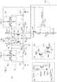
- the circuit 20 may comprise a switched current path, for instance through control terminals T, L in a pair of transistors TT 1 , TT 2 .
- the pair of transistors TT1, TT2 may have respective control terminals coupled to:
- the first transistor TT1 may have a control terminal T in the switched current path, e.g. a drain terminal, coupled to the first storage "tank" capacitance C 1 while the second transistor TT2 may have a control terminal L in the switched current path, e.g. a drain terminal, coupled to the load capacitance C L .
- the pair of transistors TT1, TT2 may comprise a pair of High Voltage n-type transistors with proper voltage class.
- transistors in the pair of transistors TT1, TT2 may have respective parasitic capacitances C P at their control terminal and respective body-drain diodes BD1, BD2.
- a bias current generator I BB may be coupled to the first common node SS.
- the circuit 20 may comprise auxiliary switches 301, 302, configured to be operated from a controller, wherein:
- auxiliary switches 301, 302 may comprise a circuit 30, as discussed in the following with respect to Figure 3 .
- the switch circuit 20 may comprise a current mirror arrangement B1, B2, M1, M2 of transistors, which may be operated as discussed in the following.
- said current mirror arrangement B1, B2, M1, M2 may comprise:
- the first subset of transistors B1, B2 may have their terminals, e.g. base terminals for bipolar transistors B1, B2, coupled to an intermediate node BB, e.g. a common base.
- the second sub-set of transistors M1, M2 may each be coupled, e.g. in series, to respective transistors B1, B2 in the first set of transistors, while at the same time having one of their respective control terminals coupled to a common node, e.g. a common gate.
- One or more embodiments may comprise a diode ZZ, e.g. Zener diode, may be coupled between the intermediate node BB and the first common node SS in order to:
- a diode ZZ e.g. Zener diode
- the circuit 20 may comprise a set of current generators Idc, Iz, Iprech.
- the set of current generators Idc, Iz, Iprech may comprise:
- the current mirror arrangement B1, B2, M1, M2 may have its output terminal, e.g. drain terminal of transistor M2, coupled to a control circuit 210, comprising:
- a control terminal of the transistor MC may be coupled to an output node of the comparator 310.
- control terminal of the transistor MC may be coupled to the output node of the comparator 310 via a digital conditioning circuit block (not visible in Figure 2 ).
- the trigger signal comp_out value may result from other logic circuits operating it, e.g. via the digital conditioning circuit block.
- the trigger signal comp_out provided as output from the comparator may be used as control signal to operate a current generator in the set of generators Idc, Iz, Iprech, for instance to operate specifically the third current generator Iprech.
- Portion c) of Figure 2 is exemplary of one or more embodiments of the reference current generator Iref, which may comprise a current generating arrangement of transistors MR1, MR2, MR3.
- a first transistor MR3 e.g. a p-type high voltage transistor
- a control terminal e.g. its source terminal
- another control terminal e.g. its drain terminal
- a pair of transistors MR1, MR2 e.g. a pair of n-type transistors
- Portion b) of Figure 2 is exemplary of one or more embodiments of a third current generator circuit Iprech and of the control circuit to operate it as a function of the signal comp_out provided by comparator 310.
- the third current generator circuit Iprech may have an inverter 312.
- the inverter 312 may be coupled to a capacitor Cprech, coupled to a resistor Rprech, e.g. in series, coupled to a transistor Mprech (e.g. a p-type high voltage transistor).
- the inverter 312 may be applied to control terminals of the transistor Mprech, configured to receive the trigger signal comp_out from comparator 310.
- the transistor Mprech may have its source terminal coupled to a high voltage level VHV at, e.g. bias high voltage level, also coupled to the resistor Rprech.
- the resistance Rprech, the capacitor Cprech and the inverter 312 may be in a level-shifter arrangement, to facilitate applying the bias voltage supply VCCA to the terminals (gate to source V GS voltage) of the transistor Mprech.
- the transistor Mprech in the pre-charge generator and the transistor MR3 in the reference generator may have sizes proportional one to another, so as to generate a correlation between the current values provided by respective generators.
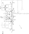
- Figure 3 is exemplary of a (per se conventional) auxiliary switch circuit 30, which may be employed in the auxiliary switches 301, 302 in the circuit 20.
- the auxiliary switch 30 may comprise a pair of transistors T 1 , T 2 , e.g. a pair of High Voltage n-type transistors with proper voltage class, which may have respective control terminals coupled:
- a diode Z e.g. a Zener diode, may be coupled between the first common node S second common node G, in order to protect the voltage drop of the transistors T1, T2 from breakdown and provide a proper value of voltage drop value.
- a first current generator I B1 may be coupled between the first common node S and ground GND, while a second current generator I B2 may be coupled between high-voltage supply and the second common node G.
- the first output terminal, e.g. a drain terminal, of the first transistor T1 may be coupled to the common node GG of TT1 and TT2, modeled as a parasitic capacitance C P while a second output terminal, e.g. a drain terminal, of the second transistor T2 may be coupled to the charge node 104 of the load capacitance C L .
- auxiliary circuit 30 will be discussed in the following a configuration like the configuration of the second auxiliary switch 302, being otherwise understood that such a configuration is not limiting, as such an auxiliary switch circuit 30 may be employed in other configurations.
- a current path couples the load capacitance C L and the parasitic capacitance C P .
- current paths across transistors T1, T2 in the auxiliary switch circuit 30 may be made conductive as a result of current generation in the first and/or second current generators I B1 and I B2 .
- a controller may operate the current generators as a function of a signal AUX_on.
- the auxiliary switches 301, 302 may be "small" with respect to the circuit 20, in order to quickly pre-charge the second common node GG of the transistors TT1, TT2, e.g. thanks to an equivalent low impedance provided by the "big" tank and load capacitances C 1 , C L .
- auxiliary switches 301, 302 may be sized so as to keep the transient time to charge-up the gate (e.g. its parasitic capacitance C P of TT1 and TT2) adequately short.
- the adequate sizing may facilitate increasing the number of steps in the charge reuse driver.
- the bias current value provided by the current generators I B1 and I B2 may be increased. For instance, as soon as one or more parasitic capacitances C P are charged up, the bias current I B1 and I B2 may flow in the Zener diode Z.
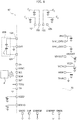
- Figure 4 is exemplary of time diagrams of a set of pre-charge signals 40 which may be employed, e.g. provided by a controller or within the circuit, to operate the circuit 20.
- one or more embodiments may involve finding out a proper sizing against process, temperature and supplies variations.
- a start-up signal SW_on provided in the first stage P1 may turn on solely the auxiliary switch in the auxiliary switches 301, 302 which is coupled to the charge node showing the lower voltage drop between tank and load terminals respective charge nodes 102, 104. For instance, such a selection may take place as a function of whether the first stage P1 belongs to the rising or falling edge of the driving signal V L .
- the pre-charge phase 40 may have a limited time duration, which facilitates reducing power consumption P as well as a fast turn on of the switch 20.
- the voltage drop at the second common node GG may be at ground level, e.g. as a consequence of a reset signal being provided.
- such a transient time in which pre-charge may be performed by the auxiliary switches 301, 302 may be provided by a correlated monostable, generating a signal AUX_on having a limited time duration.
- the signal AUX_on may be used to activate either one of 301, 302 for such limited time.
- the voltage drop on the second common node GG starts quickly to rise up from ground, e.g. up to the value of the voltage drop across either one of tank C T or load C L , as a function of the charge node terminal (102 or 104) at which the auxiliary switch 301, 302 which is active is coupled.
- the signal AUX_ON has a second value, e.g. "0" as a result of the end of the limited time duration, e.g. at P2, the first phase P1-P2 ends.
- Figure 5 and 6 are exemplary of possible operation of embodiment as per the present disclosure. In order to facilitate understanding of operation as exemplified, certain portions of Figures 5 and 6 are shown in phantom line to indicate circuit portions which may not be active in a certain operational state.
- Figure 5 shows an example of switch circuit 20 during the first stage in the interval P1-P2, e.g. as a result of signal levels as discussed in the foregoing.
- the parasitic capacitance C P of the common control terminal GG may be pre-charged 40, e.g. quickly, via the respective auxiliary switch 302, e.g. as a function of the low impedance of respective load/tank capacitance.
- the body diodes BD1, BD2 may be turned on when the node SS exceeds voltage at nodes L and/or T. For instance, this may happen: during the pre-charge phase via the auxiliary switches 301, 302 when the auxiliary switch which has been turned on is coupled to the higher voltage between the voltages in tank C 1 and load C L or during the following pre-charge phases (when the Iprech current is activated and the GG and SS nodes can rise with respect to the higher voltage between the voltages in tank C 1 or load C L ).
- the pre-charge phase via auxiliary switches may advantageously involve activating the auxiliary switch which is coupled to the lower voltage between the voltages in tank C 1 and load C L .
- auxiliary switch coupled to the higher voltage between the voltages in tank C 1 and load C L or activating both of the auxiliary switches.
- a second stage between time P2 and P3 as shown in Figure 4 may comprise signals 40 used in order to complete the turn-on of the switch circuit 20.
- At the beginning P2 of the second stage P2-P3, at least one current generator in the set of current generators Idc, Iz, Iprech may start driving the switch circuit 20 in current, in order to:
- a signal PRECH may have a first value "1" between phase P2 and P3 in order to switch on the current generators Iprech and Iz to provide:
- an increasing portion of the pre-charge current Iprech may begin to flow in the transistors B1 and B2 arranged as a current mirror pair.
- transistor B2 may mirror a current proportional or equal to the current flowing in B1, provided by the pre-charge current generator Iprech.
- the current from the current generator Iprech flows less and less towards the parasitic capacitance C P and more and more towards the current mirror B1, B2, e.g. as a result of the mirroring ration among transistors B1, B2.
- the pre-charge current Iprech may be considered completed and the pre-charge current generator Iprech may be (opportunely) turned-off.
- the current through transistor B2 may be a well-defined portion of the pre-charge current Iprech, as soon as the pre-charging 40 of parasitic capacitance C P has been completed. For instance, if B2 is equal to B1, then B2 brings half of the pre-charge Iprech.
- transistors M1 and M2 e.g. in series with transistor B1 and B2, form a cascode couple for B1 and B2, improving the mirroring among B1 and B2 transistors as well as facilitating to obtain a configuration within SOA constraints of B1 and B2 transistors.
- the cascode transistors M1, M2 are high-voltage devices.
- the mirrored current Imirr on B2 reaches the control circuit portion 210 of the switch circuit 30, where it is compared in the comparator 310 to a reference current Iref, e.g. since the mirrored current Imirr flows through a resistor R1 and the reference current from reference current generator Iref flows in resistor R2, both of which are coupled to the input nodes of the comparator, sensitive to the voltage drops on the resistors R1, R2.
- current generators may provide a correlation between reference and mirrored current values Iref, Imirr, in order to facilitate comparing such values in the comparator.
- the resistors R1, R2 may be matched correspondingly.
- the mirrored current Imirr may be a well-defined fraction of the pre-charge current Iprech, e.g. generated via the level shifter exemplified in portion b) of Figure 2 by applying a voltage VCCA to the voltage V GS of the high-voltage transistor Mprech.
- the reference current may be generated in the static circuit exemplified in portion c) of figure 2 by the transistor MR3, e.g. of the same type of the transistor Mprech opportunely sized to which a same voltage VCCA may be applied to the voltage drop V GS .
- the comparator 310 may provide a signal comp_out which, for instance:
- the comparator 310 may provide the signal comp_out indicative of the status of charging of the parasitic capacitance C P , e.g. being indicative that a portion of Iprech current which does not flow to charge the parasitic capacitance C P has reached a certain value.
- the signal comp_out may be used as a trigger signal to the pre-charge current generator Iprech, facilitating to define a, e.g. defined by design, pre-charge phase time duration. For instance, as in the example of Figure 4 , when comp_out changes value from “1” to "0", the signal PRECH as well switches from “1” to "0", indicating the end P3 of the second stage P2-P3 and operating the pre-charge generator Iprech to end generation of the current Iprech.
- the pre-charge generator Iprech can be switched-off or strongly reduced, e.g. as a result of the majority of the pre-charge current Iprech mainly flowing on the current mirror transistors B1, B2, M1, M2.
- the switch circuit 20 is hence in the condition to be completely active or "on".
- the parasitic capacitance C P may be pre-charged up to a pre-charge level, e.g. a function of a difference between the voltage at the tank node 101 and the voltage V L at said at least one charge node 104 of the load capacitance C L .
- a Direct Current (DC) generator Idc may also be turned on, e.g. at the beginning of phase P2, in order to keep a DC condition to switch-on the switch circuit 20 after the pre-charge generator Iprech is turned off at the end of phase P3, as shown in Figure 4 .
- DC Direct Current
- the signal comp_out from the comparator 310 may also, e.g. concurrently, cause the turns-off a branch B2 of the current mirror B1, B2, M1, M2.
- FIG. 6 is exemplary of the switch circuit 20 status in the second stage P2-P3 of Figure 4 and as discussed in the foregoing.
- Iref may be defined through a matched circuit (portion b of Figure 3 ).
- the second stage P3 may end when the current in transistor B2 reaches a value equal to a defined ratio of the current Iprech.
- switching "off" the generator Iprech may comprise an exponential decay phase.
- switching between a first, e.g. consistent, pre-charge bias current, in order to speed up charging parasitic capacitances C P , e.g. gate capacitance, and a second current, e.g. smaller, may be considered in order to maintain a proper and safe V GS for the rest of the transient charging phase.
- a switching circuit arrangement 20 as discussed in the foregoing may have an advantage to provide a robust SOA (Safety Operating Area) of the voltage drop V GS of transistors TT1 and TT2.
- SOA Safety Operating Area
- V GS may be the sum of diode voltage drop across the diode ZZ and a threshold voltage drop V BE .
- the current on Zener diode ZZ may be about 2/ ⁇ of the pre-charge current Iprech, facilitating to size the current keeping a voltage drop across the diode ZZ adequately low, in order not to exceed SOA limits.
- different ratio can be selected for components of different portions of the circuit (for instance, B1, B2, and/or R1, R2, ...) in order to save area and consumption.
- the switch circuit 20 may facilitate providing well controlled SOA constraints against process, temperature and supply variations.
- Figures 7 and 8 are exemplary of a circuit 70 and a device 80.
- a driver device 70 may comprise:
- the pre-store circuit block 730 may comprise circuits, known per se, to preload the tank capacitors in order to speed up device start-up, e.g. pre-charging tank capacitors to provide a voltage drop at their ends approximately equal to the value of such voltage drop in stationary periodic driving operations.
- the logic circuit block 721 may be coupled to the oscillator circuit block 740, to the pre-store circuit block 730 and to the charge reuse driver circuit block 710 and may be configured to process and provide as output, e.g. timed, control signals to the charge reuse driver 710 and to the pre-store circuit block 730.
- the driver device may comprise a plurality of pins 721p, for instance facilitating to customize the configuration of the logic circuit block 721.
- the pre-store circuit block 730 may be coupled to the charge reuse driver 710, specifically to the set of switches 200, 201, 202, 206, 20N in the charge reuse driver 710.
- the reference circuit block 760 may be coupled to the low drop-out regulator (LDO) circuit block 750, for instance providing reference voltage and current values, in a way per se known.
- LDO low drop-out regulator
- the reference circuit block 760 may provide a set of pins 760p facilitating configuration.
- the LDO circuit block 750 may provide a stable high voltage supply VHV to the charge reuse driver circuit block 710, for instance as a function of the reference voltages and currents received.
- a boost node VBOOST may be coupled to the LDO circuit block 750 and may be suitable for providing a boost bias voltage the LDO circuit block 750 in order to provide a regulated voltage level VHV.
- a boost bias voltage may be provided externally, and coupled via the boost node VBOOST, or it may be generated internally, e.g. via a DC-DC converter (also called boost converter) as a function of a low-voltage bias.
- a node VHV may facilitate providing the voltage supply VHV from an external source via the pin VHV.
- the charge reuse driver circuit block 710 may comprise a set of respective charge node pins 101, 101, 105, 106 to which a set of storage tank capacitances C 1 , C 2 , C 5 , C 6 may be coupled.
- the charge reuse driver circuit block 710 may provide at least one charge node 104 configured to be coupled to a capacitive load, e.g. a micro-mirror.
- the driver device 70 may comprise ground pins, e.g. one or more for circuit blocks, identified by the first three letters being GND.
- the driver device 70 may form a device assembly 80 comprising:
- piezoelectric load may be applied to micro-mirrors but also to other electrically powered actuators.
- one or more embodiments may be found suitable for applications such as time-of-flight, pico-projection, augmented reality and virtual reality.
- One or more embodiments comprise a method, which may comprise:
- the electronic switch circuitry (20) may comprise:
- the method may comprise providing at the charge node of the load capacitance a drive voltage signal (for instance, V L ) comprising a sequence of rising and falling edges between a supply voltage at a voltage supply node (for instance, VHV) and ground (for instance, GND), wherein:
- pre-charging said parasitic capacitance may comprise making conductive:
- pre-charging said parasitic capacitance up to a pre-charge level may be a function of a difference between the voltage at said respective charge node of an energy storage capacitance (for instance, C 1 ) in the set of energy storage capacitances and the voltage (for instance, V L ) at said at least one charge node of the load capacitance.
- the method may comprise:
- One or more embodiments may comprise a circuit, which may comprise:
- the circuit may comprise:
- One or more embodiments may comprise a device, which may comprise:
- the capacitive load may comprise a micro-mirror.
Landscapes
- Engineering & Computer Science (AREA)
- Power Engineering (AREA)
- Electronic Switches (AREA)
- Physics & Mathematics (AREA)
- Amplifiers (AREA)
- Networks Using Active Elements (AREA)
- Oscillators With Electromechanical Resonators (AREA)
- General Physics & Mathematics (AREA)
- Optics & Photonics (AREA)
Abstract
- providing a load capacitance (CL) having a charge node (104);
- providing a set of energy storage capacitances (C1), having respective charge nodes (101);
- providing electronic switch circuitry (20) configured to be made selectively conductive to couple the charge node (104) of the load capacitance (CL) to respective charge nodes (101) of energy storage capacitances (C1) in the set of energy storage capacitances (C1), wherein the electronic switch circuitry (20) comprise a switched current path (T, L) through a first transistor (TT1) and a second transistor (TT2) including junction diodes (BD1, BD2), wherein the first transistor (TT1) has a current path therethrough between a first common node (SS) and the respective charge node (101) of an energy storage capacitance (C1) in the set of energy storage capacitances (C1, C2) and the second transistor (TT2) has a current path therethrough between the first common node (SS) and the charge node (104) of the load capacitance (CL), the first transistor (TT1) and the second transistor (TT2) having control terminals mutually coupled at a second common node (GG), the control terminals having a parasitic capacitance (CP). The method comprises pre-charging the parasitic capacitance (CP) of the control terminals of the first transistor (TT1) and the second transistor (TT2) mutually coupled at the second common node (GG) prior to making conductive the switched current path (T, L) through the first transistor (TT1) and the second transistor (TT2).
Description
- The description relates to driving capacitive loads.
- Piezoelectric loads such as micro-mirrors may be exemplary of capacitive loads to which embodiments may apply.
- One or more embodiments may be applied to so-called charge reuse drivers including electronic switches, for instance high voltage and low resistance switches with fast and efficient turn-on time.
- In a charge reuse driver, a load, e.g. a capacitance, may be driven by a substantially trapezoidal signal switching between ground (0 Volt) and a high voltage VHV through rising and falling edges, which are defined by a set of sub-steps, e.g. a number N of steps.
- Such a signal may result from a stepped exchange of charge (and/or high voltage VHV) between a load capacitance and storage "tank" capacitances, the exchange comprising a set of intermediate sub-steps. For instance, in each sub-step a tank capacitance may store a respective intermediate voltage, e.g. an n-th fraction of the voltage VHV.
- During a periodic switching of the load capacitance from ground to VHV, in each sub-step, the load capacitance itself may be charged or discharged (e.g., depending on whether it is performed during the rising or falling edge of the periodic signal, respectively) through the tank capacitors.
- For a single sub-step, the amount of charge gained from the load capacitance during the rising edge may be (asymptotically) equal to the amount of charge lost during the falling edge. Thus, the load capacitance may, e.g. continuously, exchange charge with the tank capacitors.
- During the last sub-step of the falling edge, e.g. when the load capacitor is effectively discharged to ground, the charge stored in the load capacitance is lost. Such charge is subsequently recovered during the last sub-step of the rising edge, e.g. when load capacitor is connected to the supply VHV. Charge reuse drivers as known in the art provide power dissipation reduced by a factor (N-1), where N may be the number of the sub-steps.
- Charge reuse drivers may be adopted in low-voltage applications. Applying such drivers also to piezoelectric loads, e.g. to resonant micro-mirrors may be desirable.
- It is noted that voltages involved in driving loads such as micro-mirrors may often vary considerably, e.g. with trapezoidal signals possibly oscillating up to a high voltage VHV value, e.g. VHV=40V. Moreover, micro-mirrors may have intrinsic capacitances of several nanoFarads and resonance frequencies up tens of kiloHertz.
- Power dissipation may thus a figure of merit deserving consideration.
- An object of one or more embodiments is to contribute in addressing the aspects discussed above.
- According to one or more embodiments, that object can be achieved by means of a method having the features set forth in the claims that follow.
- One or more embodiments may relate to a corresponding circuit.
- One or more embodiments may relate to a corresponding device. A device comprising a charge reuse driver and a piezoelectric load (e.g. a micro-mirror) driven thereby may be exemplary of such a system.
- The claims are an integral part of the technical teaching provided herein with reference to the embodiments.
- In one or more embodiments, improved performance may be facilitated in a charge reuse driver via an increasing number of sub-steps N.
- In one or more embodiments, time devoted to rise/fall edges may be reduced (i.e. increasing the resonance frequency).
- In one or more embodiments, switching operation may use short switch turn-on times (so that rise/fall times are not appreciably affected) and (very) low switch resistance.
- One or more embodiments may involve a high-voltage switch with low resistance and (very) low turn-on times.
- In one or more embodiments, high-voltage switch devices may facilitate transferring voltages up to 40V between load and tank (or storage) capacitances, in either direction.
- One or more embodiments may adopt efficient driving circuits with well controlled safe operation area (SOA) constraints. In that respect, one or more embodiments may be based on the recognition that the turn-on transient time and the final DC resistance in a conventional switch circuit may be limited by a limited on-set resistance rON, by non-negligible parasitic capacitances and by SOA constraints.
- One or more embodiments may be based on the recognition that resorting to a set of N intermediate sub-steps may facilitate reducing power dissipation in the load (which may be expressed as the product of capacitance, voltage squared and frequency, that is P=C·V2·f) by a scale factor proportional to the number N of steps.
- One or more embodiments may comprise charge reuse drivers suitable for use in high voltage applications, in which a capacitive load being driven through a period signal. In such applications, the power dissipation is proportional to the square of the driving voltage accordingly to the formula P=C·f·V2, where C is the load capacitance, f is the switching frequency and V is the driving voltage.
- Letting each sub-step in the set of steps of the charge reuse driver (e.g. each tank capacitance) complete its transient phase - either charging or discharging the RC circuit - e.g. with 4 to 5 RC time constants may facilitate benefitting from power consumption reduction.
- On the other hand, reducing rise and fall times may be desirable in order to improve the power efficiency in applying the driving signal to the load.
- One or more embodiments will now be described, by way of non-limiting example only, with reference to the annexed Figures, wherein:
-
Figure 1 is exemplary of principles underlying one or more embodiments as per the present disclosure; -
Figure 2 is exemplary of a circuit as per the present disclosure; -
Figure 3 is exemplary of an auxiliary switch circuit embodiment; -
Figure 4 is exemplary of time diagrams of signals as discussed in the present disclosure; -
Figure 5 and6 are exemplary of portions of the exemplary circuit ofFigure 3 ; -
Figure 7 and8 are exemplary of a piezoelectric driver device as per the present disclosure. - In the ensuing description, one or more specific details are illustrated, aimed at providing an in-depth understanding of examples of embodiments of this description. The embodiments may be obtained without one or more of the specific details, or with other methods, components, materials, etc. In other cases, known structures, materials, or operations are not illustrated or described in detail so that certain aspects of embodiments will not be obscured.
- Reference to "an embodiment" or "one embodiment" in the framework of the present description is intended to indicate that a particular configuration, structure, or characteristic described in relation to the embodiment is comprised in at least one embodiment. Hence, phrases such as "in an embodiment" or "in one embodiment" that may be present in one or more points of the present description do not necessarily refer to one and the same embodiment.
- Moreover, particular conformations, structures, or characteristics may be combined in any adequate way in one or more embodiments.
- The references used herein are provided merely for convenience and hence do not define the extent of protection or the scope of the embodiments.
- Throughout the instant description of ordinal numbers, (e.g. first, second, third, ...) will be used with the purpose of facilitating the identification of components. It will be otherwise appreciated that such ordinal numbers are merely intended for that purpose and shall not be construed, even indirectly, in a limiting sense of the embodiments.
- By way of introduction to a detailed description of exemplary embodiments, reference may be first had to
Figure 1 . -
Figure 1 is exemplary of working principles of acharge reuse driver 10, e.g. which, as exemplified herein, may be used to drive a capacitive load CL, e.g. a piezoelectric actuator such as a micro-mirror. - The
charge reuse driver 10 may comprise a number N of sub-stages in which charge may be redistributed sequentially between the capacitive load CL and the N sub-stages. For the sake of simplicity, in the exemplary charge-reuse driver 10 ofFigure 1 , a number N=4 of four sub-stages is discussed, being otherwise understood that one or more embodiments may comprise virtually any number N of sub-stages. - In one or more embodiments the
charge reuse driver 10 may comprise a set ofN switches switches - In one or more embodiments, the number N of sub-stages in the
charge reuse driver 10 may comprise: - a voltage supply node VHV, e.g. a high voltage supply node with a voltage level of 40V;
- a ground node GND;
- a set of storage or "tank" capacitances C1, C2, having respective charge nodes 101,102.
- In one or more embodiments, for instance:
- a ground node GND may be couplable to the
charge node 104 of the load capacitance CL via afirst switch 200; - a first storage capacitance C1 may have its
charge node 101 couplable to thecharge node 104 of the load capacitance CL via asecond switch 201, - a second storage capacitance C2, e.g. equal to the second storage capacitance C1, may have its
charge node 102 couplable to thecharge node 104 of the load capacitance CL via athird switch 202, - the voltage supply VHV may be couplable to the
charge node 104 of the capacitive load CL via afourth switch 20N. - In one or more embodiments, switches in the set of N switches 200, 201, 202, 20N may be configured to drive the
charge node 104 of the capacitive load CL by applying thereto a sequence of rising and falling edges of a voltage signal. For instance, providing such rising and falling edges may comprise performing stages of an ordered sequence, shown inrespective portions 10a), 10b), 10c), 10d) ofFigure 1 . - In one or more embodiments, a controller (not visible in
Figure 1 ) may operate thereusable charge driver 10 to perform the sequence as exemplified inFigure 1 . - In the following, operating principles are discussed with respect to providing a rising edge, for instance initiating the sequence at
portion 10a) when: - the load capacitance CL may be discharged;
- the "tank" storage capacitances C1, C2 may store a respective equal portion of charge and have a respective equal portion of the voltage supply VHV applied at their electrodes. Specifically:
- the first tank capacitance C1 may have a voltage V1=j·VHV/(N-1)=1·VHV/3 with j=1 applied at its electrodes;
- the second tank capacitance C2 may have a voltage V2=j*VHV/(N-1)=2·VHV/3 with j=2 applied at its electrodes.
- In the charge
reuse driver system 10 as exemplified inFigure 1 , the number of tank capacitances may be equal to N-2 where N is the number of sub-steps. - In the hypothesis of driving the capacitive load CL with a periodic signal, a j-th tank capacitance reaches a voltage level of Vj=j·VHV/(N-1) con j=1, 2, ..., N-2.
-
Portions 10a) to 10d) ofFigure 1 are exemplary of producing across the load capacitance CL a "trapezoidal" voltage signal having rising edges (from ground GND to VHV) and falling edges (form VHV to ground GND). - Specifically, a "rightward" sequence from 10a) to 10d) is exemplary of a rising edge while a "leftward" sequence from 10d) to 10a) is exemplary of a falling edge.
- Providing a rising edge may comprise coupling the charge node of the load capacitance as exemplified in
Figure 1 going from 10a) to 10d). - As shown in
portion 10a) ofFigure 1 , in a first sequence stage, thecharge reuse driver 10 may close (e.g. turning on) solely thefirst switch 200, while maintaining open the remainingswitches portion 10a) ofFigure 1 , the load capacitance CL may be coupled to the ground node GND, e.g. maintaining the load capacitance CL discharged. - As shown in
portion 10b) ofFigure 1 , in a second sequence stage thecharge reuse driver 10 may close (e.g. turning on) solely thesecond switch 201, while maintaining open the remainingswitches portion 10b) ofFigure 1 , thecharge node 101 first storage capacitance C1 may be coupled to thecharge node 104 of the load capacitance CL. - It is noted that tank capacitances C1, C2, in general, may have higher capacitance values than capacitance values of the load CL to be driven, e.g. C1>>CL, C2>>CL.
- In one or more embodiments, in a generic j-th stage, e.g. during the rising edge or the falling edge, when the load capacitance CL is selectively coupled to the respective j-th tank capacitance, e.g. on the first tank capacitance C1 when the
second switch 201 is closed, a charge redistribution process may start. - As mentioned, as in general the tank capacitance C1 may have a bigger value than the load capacitance CL, the voltage drop across the load VL may reach approximately the same value of the voltage drop across the respective tank capacitance C1. In one or more embodiments, the load capacitance CL may partially receive charge from or give charge to the tank capacitance C1 as a function of whether coupling is performed while in the rising or falling edge of the ordered sequence, respectively.
- It is noted that as a result of the charging/discharging process, in one or more embodiments voltage across the tank capacitance C1 may be treated as unvaried, e.g. having a like value as a result of the process asymptotically tending to an exchange of similar charge quantities in periodic operation of the driver and of mentioned capacitances ratios C1/CL>>1.
- As shown in
portion 10c) ofFigure 1 , in a third sequence stage thecharge reuse driver 10 may close (e.g. turning on) solely thethird switch 202, while maintaining open the remainingswitches portion 10c) ofFigure 1 , thecharge node 102 of the second storage capacitance C2 may be coupled to thecharge node 104 of the load capacitance CL. - Again, similarly to what has been discussed in the foregoing with respect to
stage 10b), when the load capacitance CL is selectively coupled to the respective tank capacitance, e.g. on the second tank capacitance C2 when thethird switch 202 is closed, a charge redistribution process may start. - As shown in
portion 10d) ofFigure 1 , in a fourth sequence stage thecharge reuse driver 10 may close (e.g. turning on) solely thefourth switch 20N, while maintaining open the remainingswitches portion 10c) ofFigure 1 , the voltage supply node VHV may be coupled to thecharge node 104 of the load capacitance CL. Consequently, a process of charging the load capacitance CL may begin. At the end of the charging process, the voltage VL present at the load capacitance CL may be equal to the supply voltage VHV, e.g. VL=VHV for N=4. - It will be noted that the sequence stages 10a), 10b), 10c), 10d) may be performed in a different order with respect to the order discussed in the foregoing, e.g. beginning with the load capacitor CL charged up and moving "backwards" from
phase 10d) tophase 10a). - For instance, for a periodic input signal, the sequence may be self-sustaining, performing operations periodically oscillating from the
first stage 10a) to thefourth stage 10d and from thefourth stage 10d) tofirst stage 10a). - In one or more embodiments, the periodic driving sequence may reach a "stationary" condition for what concern the charge stored into the tank capacitors. For instance, at one sub-step on the falling edge the charge "lost" in the previous rising edge period may be "recovered".
- In one or more embodiments, a stationary condition may be reached in which tank capacitances have a "constant" (e.g. neglecting second order effects, leakage or charge injections resulting from switching) voltage across. Such a stationary condition may result from operating the charge reuse so that: at an i-th step, the load capacitance CL receives a discrete charge quantity from a respective tank capacitance C1, and at the j-th step, where j is a step involving a same tank capacitance C1 but on the opposite falling edge of the previous i-th step, e.g. when j=N+1+I, the tank C1 receives from the load CL a same discrete charge quantity to the one that was earlier (at i-th stage) transferred to the load CL. As a result, the voltage value across the load VL varies periodically employing an exchange of a same discrete charge quantity (hence the name "charge reuse") . The step of the process in which the load is coupled to ground GND is different in that a fraction of charge, e.g. 1/(N-1)*Q, is lost to ground. Such a fraction may be indicated as representative of the efficiency of the system as it may be indicated to represent the energy effectively lost (not reused) in the charge reuse driver.
- In one or more embodiments, driving a load capacitance CL according to embodiments may improve the power consumption, i.e. reducing it by a power reduction factor (N-1), where N is the number of sub-steps.
- In one or more embodiments, such improved power consumption may derive from continuously exchanging charge between load and tank, hence charge may be lost when the load is discharged onto the ground node, where the "consumed" power P may be expressed as: P=CL*f*VL 2=CL*f*VHV2/(N-1)=P0/(N-1), where P0 which may be expressed as P0=CL*f*VHV2 is the power consumption without intermediate sub-steps between voltage supply and ground.
- In one or more embodiments, increasing the number of steps N facilitates increasing the power reduction factor (N-1). For a given time-duration of the period of the periodic driving signal, e.g. trapezoidal driving signal VL comprising rising and falling edges, when the number of intermediate sub-steps is increased, so the time available for charge redistribution between tank and load capacitances CL is reduced. For instance, the time allocated for charge/discharge of the drive signal VL may be one tenth of the period of the driving signal.
- At the same time, in general, in order to get full benefits from the charge reuse approach, the charge redistribution process in each sub-step may require a certain number of time-constants, where a time constant τ is a function of tank and load capacitances value and of the resistance of the switching circuits in the set of
switches - Conventional switches, such as a
switch 30 discussed in the following with respect toFigure 3 , may lack the adequate switch time and resistance rON. In order to decrease the resistance rON, such switches may reach significative sizes, leading to an increase in a parasitic capacitance CP' at the control terminals of transistors T1, T2 which may be employed. Consequently, switch startup time may increase, due to a bigger parasitic capacitance CP' taking longer time to be charged before enabling the turn on of theswitch 30. - Hence, conventional switches may eventually reach a low on-resistance at the cost of an increase in turn-on time, making it difficult to adequately reach the desired reduction of time for charge redistribution in a j-
th sub-step - Similarly, increasing the value of the startup current provided by generators IB1 e IB2 to fasten charging a bigger capacitance leads to an undesired increased power consumption and to a (possible) excess of VGS with consequent issues to remain in a SOA (Safe Operating Area) for the switch transistors. The limited rON, not negligible driving capacitances and SOA constraints of high voltage devices may limit the turn-on transient time and final DC resistance.
- One or more embodiments may employ high-voltage devices as the voltages involved VHV, VL in the stages of the
sequence 10a), 10b), 10c), 10d) may reach high values, e.g. VHV=40 V. -
Figure 2 is exemplary of embodiments of acircuit 20, e.g. a high voltage (VHV=40V) switch circuit, which may be used in the set ofswitches - For the sake of simplicity, principles underlying embodiments will be discussed in the following with reference to the
circuit 20 in a configuration as it may be found in thesecond switch circuit 201, configured to selectively couple the first storage capacitance C1 to the load capacitance CL. It will be noted that an i-th storage capacitance may be employed in the place of the first storage capacitance C1 in the respective i-th switch, with i=1, ..., N-1. - In one or more embodiment as exemplified in portion a) of
Figure 2 , thecircuit 20 may comprise a switched current path, for instance through control terminals T, L in a pair of transistors TT1, TT2. In one or more embodiments, the pair of transistors TT1, TT2 may have respective control terminals coupled to: - a first common node SS, for instance a common source node, and
- a second common node GG, for instance a common gate node.
- In one or more embodiments, the first transistor TT1 may have a control terminal T in the switched current path, e.g. a drain terminal, coupled to the first storage "tank" capacitance C1 while the second transistor TT2 may have a control terminal L in the switched current path, e.g. a drain terminal, coupled to the load capacitance CL.
- In one or more embodiments, the pair of transistors TT1, TT2 may comprise a pair of High Voltage n-type transistors with proper voltage class.
- In one or more embodiments, transistors in the pair of transistors TT1, TT2 may have respective parasitic capacitances CP at their control terminal and respective body-drain diodes BD1, BD2.
- In one or more embodiments:
- a first pull-down switch ss1 (e.g. an electronic pull-down switch, such as a MOSFET transistor) may be configured to selectively couple the second common node GG to ground GND,
- a second pull-down switch ss2 (e.g. an electronic pull-down switch, such as a MOSFET transistor) may be configured to couple the first common node SS to ground GND.
- In one or more embodiments, a bias current generator IBB may be coupled to the first common node SS.
- In one or more embodiments, the
circuit 20 may compriseauxiliary switches - the first
auxiliary switch 301 may be coupled between the second common node GG and the control terminal T of the first transistor TT1, and - the second
auxiliary switch 302 may be coupled between the second common node GG and the control terminal L of the second transistor TT2. - In one or more embodiments,
auxiliary switches circuit 30, as discussed in the following with respect toFigure 3 . - In one or more embodiments, the
switch circuit 20 may comprise a current mirror arrangement B1, B2, M1, M2 of transistors, which may be operated as discussed in the following. - For instance, said current mirror arrangement B1, B2, M1, M2 may comprise:
- a first subset of transistors B1, B2 (e.g. a pair of p-type bipolar transistors), and
- a second subset of transistors M1, M2 (e.g. a pair of p-type high voltage transistors).
- In one or more embodiments, the first subset of transistors B1, B2 may have their terminals, e.g. base terminals for bipolar transistors B1, B2, coupled to an intermediate node BB, e.g. a common base.
- In one or more embodiments, the second sub-set of transistors M1, M2 may each be coupled, e.g. in series, to respective transistors B1, B2 in the first set of transistors, while at the same time having one of their respective control terminals coupled to a common node, e.g. a common gate.
- One or more embodiments may comprise a diode ZZ, e.g. Zener diode, may be coupled between the intermediate node BB and the first common node SS in order to:
- protect the voltage drop of the transistors TT1, TT2 from breakdown, e.g. respective gate-source voltage drops VGS, and
- provide, in addition to a voltage VBE across the transistors B1 and B2, at the same time, a proper value of voltage drop, e.g. above the threshold value, in order to turn-on the transistors TT1, TT2.
- In one or more embodiments, the
circuit 20 may comprise a set of current generators Idc, Iz, Iprech. - In one or more embodiments, the set of current generators Idc, Iz, Iprech may comprise:
- a first current generator Idc, which may be coupled to a control terminal, e.g. emitter node, of transistors B1 and B2,
- a second current generator Iz, which may be coupled to a control node of transistors B1 and B2 (e.g. in a common base configuration) and to, e.g. the negative terminal (cathode), of the diode ZZ, and
- a third current generator Iprech, which may be coupled to a control terminal, e.g. emitter node, of transistors B1 and B2.
- In one or more embodiments, the current mirror arrangement B1, B2, M1, M2 may have its output terminal, e.g. drain terminal of transistor M2, coupled to a
control circuit 210, comprising: - a transistor MC (e.g. a high voltage n-type transistor), having its output terminal, e.g. its drain terminal, coupled to the respective output terminal M2 of the current mirror arrangement B1, B2, M1, M2;
- a resistor R1 coupled to the source terminal of the transistor MC;
- a reference current generator Iref, coupled to a second resistor R2;
- a
comparator 310, coupled to the first and second resistors R1, R2 and configured to provide as output a trigger signal comp_out indicative of the comparison of respective voltage drops across respective first and second resistors R1, R2. - In one or more embodiments, a control terminal of the transistor MC may be coupled to an output node of the
comparator 310. - In one or more embodiments, the control terminal of the transistor MC may be coupled to the output node of the
comparator 310 via a digital conditioning circuit block (not visible inFigure 2 ). For instance, the digital conditioning circuit block may be configured to initialize trigger signal comp_out at an initial stage, e.g. comp_out="0", forcing the signal to go to this value in a phase in which the switch stage may not be defined. In the example considered, the trigger signal comp_out value may result from other logic circuits operating it, e.g. via the digital conditioning circuit block. - In one or more embodiments, the trigger signal comp_out provided as output from the comparator may be used as control signal to operate a current generator in the set of generators Idc, Iz, Iprech, for instance to operate specifically the third current generator Iprech.
- Portion c) of
Figure 2 is exemplary of one or more embodiments of the reference current generator Iref, which may comprise a current generating arrangement of transistors MR1, MR2, MR3. For instance, a first transistor MR3 (e.g. a p-type high voltage transistor) may have a control terminal (e.g. its source terminal) coupled to a bias voltage supply VCCA and another control terminal (e.g. its drain terminal) coupled to a pair of transistors MR1, MR2 (e.g. a pair of n-type transistors) configured as a current mirror, providing as output the reference current Iref. It is noted that the double arrow hovering on a terminal of the transistor MR2 in the pair of transistors in portion c) ofFigure 2 indicated that the current Iref provided by the exemplary circuit of portion c) offigure 2 may have a direction opposite to the direction of the current flowing in the circuit as a result of operating the current generator Iref. - Portion b) of
Figure 2 is exemplary of one or more embodiments of a third current generator circuit Iprech and of the control circuit to operate it as a function of the signal comp_out provided bycomparator 310. - In one or more embodiments the third current generator circuit Iprech may have an
inverter 312. For instance, theinverter 312 may be coupled to a capacitor Cprech, coupled to a resistor Rprech, e.g. in series, coupled to a transistor Mprech (e.g. a p-type high voltage transistor). In one or more embodiments, theinverter 312 may be applied to control terminals of the transistor Mprech, configured to receive the trigger signal comp_out fromcomparator 310. - In one or more embodiments the transistor Mprech may have its source terminal coupled to a high voltage level VHV at, e.g. bias high voltage level, also coupled to the resistor Rprech.
- In the exemplary implementation of portion b) of
Figure 2 , the resistance Rprech, the capacitor Cprech and theinverter 312 may be in a level-shifter arrangement, to facilitate applying the bias voltage supply VCCA to the terminals (gate to source VGS voltage) of the transistor Mprech. - In one or more embodiments, the transistor Mprech in the pre-charge generator and the transistor MR3 in the reference generator may have sizes proportional one to another, so as to generate a correlation between the current values provided by respective generators.
- It is noted that other current generator architectures may be employed to realize the reference current generator Iref and the pre-charge current generator Iprech discussed in the foregoing, in ways per se known.
-
Figure 3 is exemplary of a (per se conventional)auxiliary switch circuit 30, which may be employed in theauxiliary switches circuit 20. - In one or more embodiments, the
auxiliary switch 30 may comprise a pair of transistors T1, T2, e.g. a pair of High Voltage n-type transistors with proper voltage class, which may have respective control terminals coupled: - to a first common node, e.g. a common source node S, and
- to a second common node, e.g. a common gate node G.
- In one or more embodiments, a diode Z, e.g. a Zener diode, may be coupled between the first common node S second common node G, in order to protect the voltage drop of the transistors T1, T2 from breakdown and provide a proper value of voltage drop value.
- In one or more embodiments, a first current generator IB1 may be coupled between the first common node S and ground GND, while a second current generator IB2 may be coupled between high-voltage supply and the second common node G.
- In one or more embodiments:
- a first pull-down switch s1 (e.g. an electronic pull-down switch, such as a MOSFET transistor) may be coupled between the second common node G and ground GND,
- a second pull-down switch s2 (e.g. an electronic pull-down switch, such as a MOSFET transistor) may be coupled between the first common node S and ground GND.
- In one or more embodiments, the first output terminal, e.g. a drain terminal, of the first transistor T1 may be coupled to the common node GG of TT1 and TT2, modeled as a parasitic capacitance CP while a second output terminal, e.g. a drain terminal, of the second transistor T2 may be coupled to the
charge node 104 of the load capacitance CL. - For the sake of simplicity, the
auxiliary circuit 30 will be discussed in the following a configuration like the configuration of the secondauxiliary switch 302, being otherwise understood that such a configuration is not limiting, as such anauxiliary switch circuit 30 may be employed in other configurations. For instance, in one or more embodiments it may be coupled to a respective i-th tankcapacitance charge node circuit 20 via the second common node GG. - In one or more embodiments, when the
switch 30 is in a first stage, e.g. "on" or "active", a current path couples the load capacitance CL and the parasitic capacitance CP. - In one or more embodiments, current paths across transistors T1, T2 in the
auxiliary switch circuit 30 may be made conductive as a result of current generation in the first and/or second current generators IB1 and IB2. For instance, a controller may operate the current generators as a function of a signal AUX_on. - For instance, when both first S and second G common nodes are short circuited to ground GND via switches s1, s2, the
auxiliary switch 30 is "off". - Conversely, when pull-down switches s1, s2 are switched-off (e.g. being open) and current generators IB1 and IB2 are turned-on (e.g. providing respective currents), the
auxiliary switch 30 is turned-on. - In one or more embodiments the
auxiliary switches circuit 20, in order to quickly pre-charge the second common node GG of the transistors TT1, TT2, e.g. thanks to an equivalent low impedance provided by the "big" tank and load capacitances C1, CL. For instance,auxiliary switches - It is noted that, in order to facilitate speeding up the switch turn-on stage, the bias current value provided by the current generators IB1 and IB2 may be increased. For instance, as soon as one or more parasitic capacitances CP are charged up, the bias current IB1 and IB2 may flow in the Zener diode Z.
-
Figure 4 is exemplary of time diagrams of a set ofpre-charge signals 40 which may be employed, e.g. provided by a controller or within the circuit, to operate thecircuit 20. - It is noted that one or more embodiments may involve finding out a proper sizing against process, temperature and supplies variations.
- In one or more embodiments, a start-up signal SW_on having a first value, e.g. SW_on= "1", may be provided to the
switch circuit 30, initiating a first stage P1, e.g. a pre-charge stage. During this first stage starting at P1, for instance: - the
circuit 20 is not active (e.g. not driven in current IBB, Idc, Iz, Iprech), - at least one of the
auxiliary switches - Specifically, a start-up signal SW_on provided in the first stage P1 may turn on solely the auxiliary switch in the
auxiliary switches respective charge nodes - In one or more embodiments, the
pre-charge phase 40 may have a limited time duration, which facilitates reducing power consumption P as well as a fast turn on of theswitch 20. - In one or more embodiments, before the start-up signal SW_on is provided, the voltage drop at the second common node GG may be at ground level, e.g. as a consequence of a reset signal being provided.
- In one or more embodiments, such a transient time in which pre-charge may be performed by the
auxiliary switches - In one or more embodiments, during the time in which at least one
auxiliary switch auxiliary switch -
Figure 5 and6 are exemplary of possible operation of embodiment as per the present disclosure. In order to facilitate understanding of operation as exemplified, certain portions ofFigures 5 and6 are shown in phantom line to indicate circuit portions which may not be active in a certain operational state. -
Figure 5 shows an example ofswitch circuit 20 during the first stage in the interval P1-P2, e.g. as a result of signal levels as discussed in the foregoing. - For the sake of brevity, like reference numerals/symbols are used in
Figure 5 andFigure 2 to indicate like circuit portions. - For instance, during the first stage P1-P2, as shown by the dashed arrows in
Figure 5 , if the load capacitance CL stores a voltage lower than the voltage stored on the tank capacitor C1 (as e.g. in the case discussed with respect to portion b) ofFigure 1 , where the tank capacitor is already indicated as C1), then theauxiliary switch 302 is activated. - In one or more embodiments, the parasitic capacitance CP of the common control terminal GG may be pre-charged 40, e.g. quickly, via the respective
auxiliary switch 302, e.g. as a function of the low impedance of respective load/tank capacitance. - In the example considered, while the parasitic capacitance CP charging process is ongoing, voltage level at the common control terminal GG may increase consequently, and a portion of the current may begin to flow into the current mirror arrangement transistors B1, B2, M1, M2 and the Zener diode ZZ towards the second common control terminal SS. Voltage level at the second common control terminal SS may increase consequently, e.g. gradually. Hence, in the example considered, respective body diode junctions BD1, BD2 may be weakly turned-on.
- In one or more embodiments, the body diodes BD1, BD2 may be turned on when the node SS exceeds voltage at nodes L and/or T. For instance, this may happen: during the pre-charge phase via the
auxiliary switches - In one or more embodiments, the pre-charge phase via auxiliary switches may advantageously involve activating the auxiliary switch which is coupled to the lower voltage between the voltages in tank C1 and load CL.
- In one or more embodiments, it may also be possible to activate the auxiliary switch coupled to the higher voltage between the voltages in tank C1 and load CL or activating both of the auxiliary switches.
- At this point, a second stage between time P2 and P3 as shown in
Figure 4 may comprisesignals 40 used in order to complete the turn-on of theswitch circuit 20. - In one or more embodiments, at the beginning P2 of the second stage P2-P3, at least one current generator in the set of current generators Idc, Iz, Iprech may start driving the
switch circuit 20 in current, in order to: - complete the charging of its common gate GG above the maximum voltage between
load 104 andtank 101 respective nodes, and - to provide a proper voltage drop VGS between first SS and second GG common nodes.
- In one or more embodiments, a signal PRECH may have a first value "1" between phase P2 and P3 in order to switch on the current generators Iprech and Iz to provide:
- a pre-charge current Iprech from the third pre-charge generator Iprech, e.g. non-negligible, to fast complete the charging of the common node GG of the
switch circuit 20, and - a diode current Iz from the diode current generator Iz, e.g. small, to keep a voltage of 2-3V across the Zener diode ZZ.
- In one or more embodiments, at the beginning of the second stage P2-P3:
- AUX_on may go to or remain in a second state, e.g. AUX_on="0" and the
auxiliary switch 302 may be deactivated; - the majority of the pre-charge current Iprech from the third generator flows to charge the parasitic capacitance CP, e.g. of the second transistors TT1 and TT2 as discussed in the example of
Figure 5 . - In one or more embodiments, as soon as the parasitic capacitance CP may have a charge close to its final value, e.g. maximum value, an increasing portion of the pre-charge current Iprech may begin to flow in the transistors B1 and B2 arranged as a current mirror pair.
- In one or more embodiments, transistor B2 may mirror a current proportional or equal to the current flowing in B1, provided by the pre-charge current generator Iprech.
- For instance, while approaching the full charge of the parasitic capacitance, the current from the current generator Iprech flows less and less towards the parasitic capacitance CP and more and more towards the current mirror B1, B2, e.g. as a result of the mirroring ration among transistors B1, B2.
- For instance, when at least a consistent portion of the pre-charge current Iprech flows through current mirror transistors B1 (and B2) and is closed onto load CL and/or tank capacitance C1 via body diodes BD1 (and BD2) and transistors TT1 (and TT2) turned (partially) on, the pre-charge of the parasitic capacitance CP may be considered completed and the pre-charge current generator Iprech may be (opportunely) turned-off.
- Hence, the current through transistor B2 may be a well-defined portion of the pre-charge current Iprech, as soon as the
pre-charging 40 of parasitic capacitance CP has been completed. For instance, if B2 is equal to B1, then B2 brings half of the pre-charge Iprech. - In one or more embodiments, transistors M1 and M2, e.g. in series with transistor B1 and B2, form a cascode couple for B1 and B2, improving the mirroring among B1 and B2 transistors as well as facilitating to obtain a configuration within SOA constraints of B1 and B2 transistors. In one or more embodiments, the cascode transistors M1, M2 are high-voltage devices.
- In one or more embodiments, thanks to current mirroring B1, B2, M1, M2, the mirrored current Imirr on B2 reaches the
control circuit portion 210 of theswitch circuit 30, where it is compared in thecomparator 310 to a reference current Iref, e.g. since the mirrored current Imirr flows through a resistor R1 and the reference current from reference current generator Iref flows in resistor R2, both of which are coupled to the input nodes of the comparator, sensitive to the voltage drops on the resistors R1, R2. - In one or more embodiments, current generators, as exemplified in portions b) and c) of
Figure 2 , may provide a correlation between reference and mirrored current values Iref, Imirr, in order to facilitate comparing such values in the comparator. - In one or more embodiments, as a result, the resistors R1, R2 may be matched correspondingly.
- For instance, the mirrored current Imirr may be a well-defined fraction of the pre-charge current Iprech, e.g. generated via the level shifter exemplified in portion b) of
Figure 2 by applying a voltage VCCA to the voltage VGS of the high-voltage transistor Mprech. - For instance, the reference current may be generated in the static circuit exemplified in portion c) of
figure 2 by the transistor MR3, e.g. of the same type of the transistor Mprech opportunely sized to which a same voltage VCCA may be applied to the voltage drop VGS. - As a result, in the example discussed, the current values of Iprech and Iref are correlated precisely, neglecting second order effects (e.g. manufacturing process spread, temperature, voltage supply, ripples...) which may be fixed with methods per se known.
- In one or more embodiments, the
comparator 310 may provide a signal comp_out which, for instance: - has a first value, e.g. comp_out= "1", if the mirrored current Imirr is lower than the reference current Iref;
- has a second value, e.g. comp_out="0", if the mirrored current Imirr equals or exceeds the reference current Iref.
- In one or more embodiments, the
comparator 310 may provide the signal comp_out indicative of the status of charging of the parasitic capacitance CP, e.g. being indicative that a portion of Iprech current which does not flow to charge the parasitic capacitance CP has reached a certain value. - In one or more embodiments, the signal comp_out may be used as a trigger signal to the pre-charge current generator Iprech, facilitating to define a, e.g. defined by design, pre-charge phase time duration. For instance, as in the example of
Figure 4 , when comp_out changes value from "1" to "0", the signal PRECH as well switches from "1" to "0", indicating the end P3 of the second stage P2-P3 and operating the pre-charge generator Iprech to end generation of the current Iprech. - In one or more embodiments, as a function of the trigger signal comp_out, the pre-charge generator Iprech can be switched-off or strongly reduced, e.g. as a result of the majority of the pre-charge current Iprech mainly flowing on the current mirror transistors B1, B2, M1, M2.
- In one or more embodiments, at the end P3 of the second phase P2-P3, the
switch circuit 20 is hence in the condition to be completely active or "on". - In one or more embodiments, the parasitic capacitance CP may be pre-charged up to a pre-charge level, e.g. a function of a difference between the voltage at the
tank node 101 and the voltage VL at said at least onecharge node 104 of the load capacitance CL. - In one or more embodiments, a Direct Current (DC) generator Idc may also be turned on, e.g. at the beginning of phase P2, in order to keep a DC condition to switch-on the
switch circuit 20 after the pre-charge generator Iprech is turned off at the end of phase P3, as shown inFigure 4 . - In one or more embodiments, the signal comp_out from the
comparator 310 may also, e.g. concurrently, cause the turns-off a branch B2 of the current mirror B1, B2, M1, M2. -
Figure 6 is exemplary of theswitch circuit 20 status in the second stage P2-P3 ofFigure 4 and as discussed in the foregoing. - For the sake of brevity, like reference numerals/symbols are used in
Figure 3 andFigure 6 to indicate same circuit portions. - In one or more embodiments, as Iref may be defined through a matched circuit (portion b of
Figure 3 ). - In one or more embodiments, the second stage P3 may end when the current in transistor B2 reaches a value equal to a defined ratio of the current Iprech.
- For instance:
- a best turn-on performance may end the phase P3 when the current in the current mirror B1, B2 has a ratio about 4/5 of the pre-charge current Iprech, e.g. Imirr=0.8*Iprech.
- the
circuit 20 may reach very fast turn-on time (e.g. about 20-30 ns, where 1 ns=10-9 s=1 nanosecond) associated to a low DC resistance (e.g. less than 25 Ohm). - In one or more embodiments, switching "off" the generator Iprech may comprise an exponential decay phase.
- In one or more embodiments, switching between a first, e.g. consistent, pre-charge bias current, in order to speed up charging parasitic capacitances CP, e.g. gate capacitance, and a second current, e.g. smaller, may be considered in order to maintain a proper and safe VGS for the rest of the transient charging phase.
- It is noted that a
switching circuit arrangement 20 as discussed in the foregoing may have an advantage to provide a robust SOA (Safety Operating Area) of the voltage drop VGS of transistors TT1 and TT2. For instance, such voltage drop VGS may be the sum of diode voltage drop across the diode ZZ and a threshold voltage drop VBE. - In one or more embodiments, the current on Zener diode ZZ may be about 2/β of the pre-charge current Iprech, facilitating to size the current keeping a voltage drop across the diode ZZ adequately low, in order not to exceed SOA limits. For instance, sizing of the pre-charge current Iprech may take into account the diode Zener law, e.g. VZ=VZ(IZ), so that the voltage across the Zener diode is kept at an adequately high value to guarantee the turn-on of TT1 and TT2 transistors (together with the VBE of B1 and B2) while being also kept at a value adequately low not to arise SOA issues.
- As mentioned, in one or more embodiments different ratio can be selected for components of different portions of the circuit (for instance, B1, B2, and/or R1, R2, ...) in order to save area and consumption.
- In one or more embodiments, the
switch circuit 20 may facilitate providing well controlled SOA constraints against process, temperature and supply variations. -
Figures 7 and8 are exemplary of acircuit 70 and adevice 80. - In an exemplary embodiment as shown in
Figure 7 , adriver device 70 may comprise: - a charge reuse
driver circuit block 710, comprising a set ofswitches circuit 20 therein and be configured to be operated according to one or more embodiments, as discussed in the foregoing; - a
logic circuit block 721, e.g. digital logic circuit block, which may comprise thecontrol circuit portion 210 of theswitch circuit 20; - a
pre-store circuit block 730, - an
oscillator circuit block 740, e.g. a monostable circuit, which may provide a clock signal to thelogic circuit block 730, e.g. for timing signals; - a low drop-out regulator (LDO)
circuit block 750, providing bias supply voltages, e.g. high voltages, - a
reference circuit block 760, e.g. bandgap circuits, providing the reference current Iref or a reference voltage. - In one or more embodiments, the
pre-store circuit block 730 may comprise circuits, known per se, to preload the tank capacitors in order to speed up device start-up, e.g. pre-charging tank capacitors to provide a voltage drop at their ends approximately equal to the value of such voltage drop in stationary periodic driving operations. - In one or more embodiments, the
logic circuit block 721 may be coupled to theoscillator circuit block 740, to thepre-store circuit block 730 and to the charge reusedriver circuit block 710 and may be configured to process and provide as output, e.g. timed, control signals to thecharge reuse driver 710 and to thepre-store circuit block 730. - In one or more embodiments, the driver device may comprise a plurality of pins 721p, for instance facilitating to customize the configuration of the
logic circuit block 721. - In one or more embodiments, the
pre-store circuit block 730 may be coupled to thecharge reuse driver 710, specifically to the set ofswitches charge reuse driver 710. - In one or more embodiments, the
reference circuit block 760 may be coupled to the low drop-out regulator (LDO)circuit block 750, for instance providing reference voltage and current values, in a way per se known. - In one or more embodiments, the
reference circuit block 760 may provide a set ofpins 760p facilitating configuration. - In one or more embodiments, the
LDO circuit block 750 may provide a stable high voltage supply VHV to the charge reusedriver circuit block 710, for instance as a function of the reference voltages and currents received. - In one or more embodiments, a boost node VBOOST may be coupled to the
LDO circuit block 750 and may be suitable for providing a boost bias voltage theLDO circuit block 750 in order to provide a regulated voltage level VHV. For instance, such a boost bias voltage may be provided externally, and coupled via the boost node VBOOST, or it may be generated internally, e.g. via a DC-DC converter (also called boost converter) as a function of a low-voltage bias. - In one or more embodiments, a node VHV may facilitate providing the voltage supply VHV from an external source via the pin VHV.
- In one or more embodiments, the charge reuse
driver circuit block 710 may comprise a set of respective charge node pins 101, 101, 105, 106 to which a set of storage tank capacitances C1, C2, C5, C6 may be coupled. - In one or more embodiments, the charge reuse
driver circuit block 710 may provide at least onecharge node 104 configured to be coupled to a capacitive load, e.g. a micro-mirror. - In one or more embodiments, the
driver device 70 may comprise ground pins, e.g. one or more for circuit blocks, identified by the first three letters being GND. - As shown in the exemplary embodiment of
Figure 8 , thedriver device 70 may form adevice assembly 80 comprising: - a plurality of tank capacitors C1, C2, C5, C6, e.g. coupled, e.g. soldered, to respective charge node pins 101, 102, 105, 106;
- at least one capacitive load CL, for instance of a
piezoelectric actuator 800, coupled to the respective at least onecharge node 104 of the charge reusedriver circuit block 710 in thedriver device 70; - an interface A, e.g. a digital interface;
- optional capacitances, e.g. coupled to respective pins indicated as VREF, VHV_LDO, VHV;
- a set of voltage sources, e.g. coupled to respective pins VCCA, VBOOST in the
device assembly 80. - In one or more embodiments, a number N of capacitances for the charge reuse
driver circuit block 710 may be fixated to the pins, e.g. N=4 capacitances soldered to the pins, while series resistances between tank capacitances C1, C2, C5, C6 are preferably minimized. - For instance, each tank capacitance may have a given value, e.g. C1=C2=C5=C6=220nF (1nF=1nanoFarad=10-9Farad).
- In one or more embodiments, optional capacitances may have a value equal to the value of tank capacitance or different values, e.g. the capacitance coupled to the pin VREF may be equal to 220nF, while the capacitance coupled to the pin VHV may have a value of 1microFarad (1microFarad=10-6Farad).
- It is noted that what discussed herein with respect to the driver device and circuit for a piezoelectric load may be applied to micro-mirrors but also to other electrically powered actuators. For instance, one or more embodiments may be found suitable for applications such as time-of-flight, pico-projection, augmented reality and virtual reality.
- One or more embodiments comprise a method, which may comprise:
- providing a load capacitance (for instance, CL) having a charge node (for instance, 104);
- providing a set of energy storage capacitances (for instance, C1, C2), having respective charge nodes (for instance, 101, 102);
- providing electronic switch circuitry (for instance, 20) configured to be made selectively conductive to couple the charge node of the load capacitance to respective charge nodes of energy storage capacitances in the set of energy storage capacitances, wherein the electronic switch circuitry comprise a switched current path (for instance, T, L) through a first transistor (for instance, TT1) and a second transistor (for instance, TT2) including junction diodes (for instance, BD1, BD2), wherein the first transistor (for instance, TT1) has a current path therethrough between a first common node (for instance, SS) and the respective charge node of an energy storage capacitance (for instance, C1) in the set of energy storage capacitances and the second transistor has a current path therethrough between the first common node and the charge node of the load capacitance, the first transistor and the second transistor having control terminals mutually coupled at a second common node (for instance, GG), the control terminals having a parasitic capacitance (for instance, CP),
- In one or more embodiments, the electronic switch circuitry (20) may comprise:
- a) a first auxiliary switched (for instance, 301) current path between the second common node and said respective charge node of an energy storage capacitance (for instance, C1) in the set of energy storage capacitances,
- b) a second auxiliary switched (for instance, 302) current path between the second common node and the charge node of the load capacitance,
- In one or more embodiments, the method may comprise providing at the charge node of the load capacitance a drive voltage signal (for instance, VL) comprising a sequence of rising and falling edges between a supply voltage at a voltage supply node (for instance, VHV) and ground (for instance, GND), wherein:
- a) at said rising edges, the charge node of the load capacitance is subsequently coupled, in an ordered sequence:
- to ground,
- to respective charge nodes (for instance, 101, 102) of the energy storage capacitances in the set of energy storage capacitances to receive charge therefrom, and
- to said voltage supply node, and
- b) at said falling edges, the charge node of the load capacitance is subsequently coupled, in an ordered sequence:
- to said voltage supply node,
- to respective charge nodes of energy storage capacitances in the set of energy storage capacitances to transfer charge thereto, and
- to ground.
- In one or more embodiments:
- said drive voltage signal may comprise an alternated sequence of rising and falling edges, and
- pre-charging said parasitic capacitance may comprise an alternated sequence of making conductive said first and said second auxiliary switched current paths.
- In one or more embodiments, pre-charging said parasitic capacitance may comprise making conductive:
- the first auxiliary switched current path (for instance, 301) at said falling edges, and
- the second auxiliary switched current path (for instance, 302) at said rising edges.
- In one or more embodiments, pre-charging said parasitic capacitance up to a pre-charge level may be a function of a difference between the voltage at said respective charge node of an energy storage capacitance (for instance, C1) in the set of energy storage capacitances and the voltage (for instance, VL) at said at least one charge node of the load capacitance.
- In one or more embodiments, the method may comprise:
- sensing (for instance, B1, B2, M1, M2, Mc) a pre-charge current (for instance, Iprech) pre-charging the parasitic capacitance (for instance, Cp) of the control terminals of the first transistor and second transistor,
- discontinuing (for instance, P3, comp_out, PRECH) pre-charging the parasitic capacitances (for instance, Cp) of the control terminals of the first transistor (for instance, TT1) and second transistor (for instance, TT2) as a result of the intensity of the pre-charge current sensed (for instance, Iprech, Imirr) reaching a reference intensity value (for instance, Iref).
- One or more embodiments may comprise a circuit, which may comprise:
- a load charge node (for instance, 104) configured to be coupled to a load capacitance (for instance, CL);
- an energy storage charge node (for instance, 101) configured to be coupled to an energy storage capacitance (for instance, C1),
- electronic switch circuitry (for instance, 20) configured to be made selectively conductive to couple the load charge node to the energy storage node, wherein the electronic switch circuitry (for instance, 20) comprise a switched current path (for instance, T, L) through a first transistor (for instance, TT1) and a second transistor (for instance, TT2) including junction diodes (for instance, BD1, BD2), wherein the first transistor has a current path therethrough between a first common node (for instance, SS) and the energy storage charge node and the second transistor has a current path therethrough between the first common node and the load charge node, the first transistor and the second transistor having control terminals mutually coupled at a second common node (for instance, GG), the control terminals having a parasitic capacitance (for instance, CP),
- In one or more embodiments, the circuit may comprise:
- at least one pre-charge current generator (for instance, Iprech) coupled to the second common node to provide said pre-charge current at the second common node,
- a comparator circuit (for instance, R1, R2, 310, 210) configured (for instance, B1, B2, M1, M2, MC) to:
- compare with a reference intensity value (for instance, Iref) the intensity of the pre-charge current (for instance, Iprech, Imirr),
- provide a de-activation signal (for instance, comp_out) to the pre-charge generator (for instance, Iprech) to discontinue (for instance, P3) pre-charging (for instance, 40) the parasitic capacitance (for instance, CP) of the control terminals of the first transistor and second transistor as a result of the intensity of the pre-charge current sensed (for instance, Iprech, Imirr) reaching the reference intensity value (for instance, Iref), and
- current mirror circuitry (for instance, B1, B2, M1, M2) intermediate the at least one pre-charge current generator and the comparator circuit the current mirror circuitry configured to mirror towards the comparator circuit the pre-charge current provided by the at least one pre-charge current generator.
- One or more embodiments may comprise a device, which may comprise:
- at least one circuit according to one or more embodiments,
- a capacitive load (for instance, 800) coupled to the said load charge node (for instance, 104) and providing load capacitance (for instance, CL) at said charge node (104).
- In one or more embodiments:
- the capacitive load may comprise a piezoelectric load, and/or
- the load charge node may be configured to be selectively coupled to a voltage supply node (for instance, VHV) at a voltage up to 40V.
- In one or more embodiments, the capacitive load may comprise a micro-mirror.
- It will be otherwise understood that the various individual implementing options exemplified throughout the figures accompanying this description are not necessarily intended to be adopted in the same combinations exemplified in the figures. One or more embodiments may thus adopt these (otherwise non-mandatory) options individually and/or in different combinations with respect to the combination exemplified in the accompanying figures.
- Without prejudice to the underlying principles, the details and embodiments may vary, even significantly, with respect to what has been described by way of example only, without departing from the extent of protection. The extent of protection is defined by the annexed claims.
Claims (12)
- A method, comprising:- providing a load capacitance (CL) having a charge node (104);- providing a set of energy storage capacitances (C1, C2), having respective charge nodes (101, 102);- providing electronic switch circuitry (20) configured to be made selectively conductive to couple the charge node (104) of the load capacitance (CL) to respective charge nodes (101, 102) of energy storage capacitances (C1, C2) in the set of energy storage capacitances (C1, C2), wherein the electronic switch circuitry (20) comprise a switched current path (T, L) through a first transistor (TT1) and a second transistor (TT2) including junction diodes (BD1, BD2), wherein the first transistor (TT1) has a current path therethrough between a first common node (SS) and the respective charge node (101) of an energy storage capacitance (C1) in the set of energy storage capacitances (C1, C2) and the second transistor (TT2) has a current path therethrough between the first common node (SS) and the charge node (104) of the load capacitance (CL), the first transistor (TT1) and the second transistor (TT2) having control terminals mutually coupled at a second common node (GG), the control terminals having a parasitic capacitance (CP),wherein the method comprises pre-charging (40) the parasitic capacitance (CP) of the control terminals of the first transistor (TT1) and the second transistor (TT2) mutually coupled at the second common node (GG) prior to making conductive the switched current path (T, L) through the first transistor (TT1) and the second transistor (TT2).
- The method of claim 1, wherein the electronic switch circuitry (20) comprise:- a) a first auxiliary switched (301) current path between the second common node (GG) and said respective charge node (101) of an energy storage capacitance (C1) in the set of energy storage capacitances (C1, C2),- b) a second auxiliary switched (302) current path between the second common node (GG) and the charge node (104) of the load capacitance (CL),wherein pre-charging (40) said parasitic capacitance (CP) comprises making conductive (AUX_on) either one of said first (301) and second (302) auxiliary switched current paths.
- The method of claim 1 or claim 2, comprising providing at the charge node (104) of the load capacitance (CL) a drive voltage signal (VL) comprising a sequence of rising and falling edges between a supply voltage at a voltage supply node (VHV) and ground (GND), wherein:- a) at said rising edges, the charge node (104) of the load capacitance (CL) is subsequently coupled, in an ordered sequence:- to ground (GND),- to respective charge nodes (101, 102) of the energy storage capacitances (C1, C2) in the set of energy storage capacitances (C1, C2) to receive charge therefrom, and- to said voltage supply node (VHV), and- b) at said falling edges, the charge node (104) of the load capacitance (CL) is subsequently coupled, in an ordered sequence:- to said voltage supply node (VHV),- to respective charge nodes (101, 102) of energy storage capacitances (C1, C2) in the set of energy storage capacitances (C1, C2) to transfer charge thereto, and- to ground (GND).
- The method of claim 2 and claim 3, wherein:- said drive voltage signal (VL) comprises an alternated sequence of rising and falling edges, and- pre-charging (40) said parasitic capacitance (CP) comprises an alternated sequence of making conductive (AUX_on) said first (301) and said second (302) auxiliary switched current paths.
- The method of claim 2 and claim 3, wherein pre-charging (40) said parasitic capacitance (CP) comprises making conductive (AUX_on):- the first auxiliary switched current path (301) at said falling edges, and- the second auxiliary switched current path (302) at said rising edges.
- The method of any of previous claims, comprising pre-charging (40) said parasitic capacitance (CP) up to a pre-charge level which is a function of a difference between the voltage at said respective charge node (101) of an energy storage capacitance (C1) in the set of energy storage capacitances (C1, C2) and the voltage (VL) at said at least one charge node (104) of the load capacitance (CL).
- The method of any of previous claims, comprising:- sensing (B1, B2, M1, M2, Mc) a pre-charge current (Iprech) pre-charging the parasitic capacitance (CP) of the control terminals of the first transistor (TT1) and second transistor (TT2),- discontinuing (P3, comp_out, PRECH) pre-charging the parasitic capacitances (CP) of the control terminals of the first transistor (TT1) and second transistor (TT2) as a result of the intensity of the pre-charge current sensed (Iprech, Imirr) reaching a reference intensity value (Iref).
- A circuit comprising:- a load charge node (104) configured to be coupled to a load capacitance (CL);- an energy storage charge node (101) configured to be coupled to an energy storage capacitance (C1),- electronic switch circuitry (20) configured to be made selectively conductive to couple the load charge node (104) to the energy storage node (101), wherein the electronic switch circuitry (20) comprise a switched current path (T, L) through a first transistor (TT1) and a second transistor (TT2) including junction diodes (BD1, BD2), wherein the first transistor (TT1) has a current path therethrough between a first common node (SS) and the energy storage charge node (101) and the second transistor (TT2) has a current path therethrough between the first common node (SS) and the load charge node (104), the first transistor (TT1) and the second transistor (TT2) having control terminals mutually coupled at a second common node (GG), the control terminals having a parasitic capacitance (CP),wherein the circuit comprises pre-charge circuitry (301, 302) configured to operate with the method of any of claims 1 to 7 to pre-charge (40) the parasitic capacitance (CP) of the control terminals of the first transistor (TT1) and the second transistor (TT2) mutually coupled at the second common node (GG).
- The circuit of claim 8 configured to operate with the method of claim 7, comprising:- at least one pre-charge current generator (Iprech) coupled to the second common node (GG) to provide said pre-charge current at the second common node (GG),- a comparator circuit (R1, R2, 310, 210) configured (B1, B2, M1, M2, MC) to:- compare with a reference intensity value (Iref) the intensity of the pre-charge current (Iprech) provided by the at least one pre-charge current generator (Iprech),- provide a de-activation signal (comp_out) to the pre-charge generator (Iprech) to discontinue (P3) pre-charging (40) the parasitic capacitance (CP) of the control terminals of the first transistor (TT1) and second transistor (TT2) as a result of the intensity of the pre-charge current sensed (Iprech) reaching the reference intensity value (Iref), and- current mirror circuitry (B1, B2, M1, M2) intermediate the at least one pre-charge current generator (Iprech) and the comparator circuit (R1, R2, 210) the current mirror circuitry (B1, B2, M1, M2) configured to mirror towards the comparator circuit (R1, R2, 210) the pre-charge current (Iprech) provided by the at least one pre-charge current generator (Iprech).
- A device, comprising:- at least one circuit according to claim 8 or claim 9,- a capacitive load (800) coupled to the said load charge node (104) and providing load capacitance (CL) at said charge node (104).
- The device of claim 10, wherein:- the capacitive load (800) comprises a piezoelectric load, and/or- the load charge node (104) is configured to be selectively coupled to a voltage supply node (VHV) at a voltage up to 40V.
- The device of claim 10 or claim 11, wherein the capacitive load (800) comprises a micro-mirror.
Applications Claiming Priority (1)
| Application Number | Priority Date | Filing Date | Title |
|---|---|---|---|
| IT102019000001023A IT201900001023A1 (en) | 2019-01-23 | 2019-01-23 | PROCEDURE FOR DRIVING A CORRESPONDING CAPACITIVE LOAD, CIRCUIT AND DEVICE |
Publications (2)
| Publication Number | Publication Date |
|---|---|
| EP3687068A1 true EP3687068A1 (en) | 2020-07-29 |
| EP3687068B1 EP3687068B1 (en) | 2023-06-14 |
Family
ID=66049617
Family Applications (1)
| Application Number | Title | Priority Date | Filing Date |
|---|---|---|---|
| EP20151638.2A Active EP3687068B1 (en) | 2019-01-23 | 2020-01-14 | A method of driving a capacitive load, corresponding circuit and device |
Country Status (3)
| Country | Link |
|---|---|
| US (1) | US11581892B2 (en) |
| EP (1) | EP3687068B1 (en) |
| IT (1) | IT201900001023A1 (en) |
Families Citing this family (2)
| Publication number | Priority date | Publication date | Assignee | Title |
|---|---|---|---|---|
| US11121713B1 (en) * | 2020-08-14 | 2021-09-14 | Analog Devices, Inc. | Boosted switch drivers for high-speed signal switching |
| KR102787124B1 (en) * | 2022-11-21 | 2025-03-25 | 연세대학교 산학협력단 | Circuit for detecting capacitance with dynamic current mirror |
Citations (5)
| Publication number | Priority date | Publication date | Assignee | Title |
|---|---|---|---|---|
| DE19858250A1 (en) * | 1998-12-17 | 2000-06-21 | Bosch Gmbh Robert | Charging and discharging of piezoelectric element whilst carrying out charge transport from element having capacitive characteristics to the piezoelectric element or vice versa |
| US20080238527A1 (en) * | 2003-10-06 | 2008-10-02 | Siemens Ag | Switching Device for Bi-Directionally Equalizing Charge Between Energy Accumulators and Corresponding Methods |
| US20100321089A1 (en) * | 2009-05-04 | 2010-12-23 | Choy Benedict C K | Complementary high voltage switched current source integrated circuit |
| US20110018919A1 (en) * | 2009-07-21 | 2011-01-27 | Seiko Epson Corporation | Capacitive load driving circuit, liquid ejection device, and printing apparatus |
| EP3206278A1 (en) * | 2014-10-08 | 2017-08-16 | Hong Kong Polytechnic University | Voltage balancing circuit |
-
2019
- 2019-01-23 IT IT102019000001023A patent/IT201900001023A1/en unknown
-
2020
- 2020-01-09 US US16/738,419 patent/US11581892B2/en active Active
- 2020-01-14 EP EP20151638.2A patent/EP3687068B1/en active Active
Patent Citations (5)
| Publication number | Priority date | Publication date | Assignee | Title |
|---|---|---|---|---|
| DE19858250A1 (en) * | 1998-12-17 | 2000-06-21 | Bosch Gmbh Robert | Charging and discharging of piezoelectric element whilst carrying out charge transport from element having capacitive characteristics to the piezoelectric element or vice versa |
| US20080238527A1 (en) * | 2003-10-06 | 2008-10-02 | Siemens Ag | Switching Device for Bi-Directionally Equalizing Charge Between Energy Accumulators and Corresponding Methods |
| US20100321089A1 (en) * | 2009-05-04 | 2010-12-23 | Choy Benedict C K | Complementary high voltage switched current source integrated circuit |
| US20110018919A1 (en) * | 2009-07-21 | 2011-01-27 | Seiko Epson Corporation | Capacitive load driving circuit, liquid ejection device, and printing apparatus |
| EP3206278A1 (en) * | 2014-10-08 | 2017-08-16 | Hong Kong Polytechnic University | Voltage balancing circuit |
Also Published As
| Publication number | Publication date |
|---|---|
| EP3687068B1 (en) | 2023-06-14 |
| US20200233206A1 (en) | 2020-07-23 |
| US11581892B2 (en) | 2023-02-14 |
| IT201900001023A1 (en) | 2020-07-23 |
Similar Documents
| Publication | Publication Date | Title |
|---|---|---|
| US10686377B1 (en) | Start-up method and apparatus for boost converters | |
| US10498229B2 (en) | Method and circuitry to soft start high power charge pumps | |
| CN101364118B (en) | Regulator and high voltage generator | |
| JP2703706B2 (en) | Charge pump circuit | |
| US7843712B2 (en) | Charge pump for positive pumping and negative pumping | |
| US20030214346A1 (en) | Charge pump for negative voltages | |
| US10483846B1 (en) | Multi-mode charge pump | |
| US11139004B2 (en) | Charge pump circuit and auxiliary power supply | |
| US20130241515A1 (en) | Semiconductor device | |
| US9653990B1 (en) | Negative charge pump with soft start | |
| US10447257B2 (en) | Semiconductor device | |
| EP3687068B1 (en) | A method of driving a capacitive load, corresponding circuit and device | |
| US9423814B2 (en) | Apparatus of supplying power while maintaining its output power signal and method therefor | |
| US7719245B2 (en) | Methods and apparatus to provide self-tracking pre-driver controls | |
| USRE39274E1 (en) | Voltage down converter with switched hysteresis | |
| US20240128852A1 (en) | Gate-control of a power-switch in a switching converter | |
| CN101449451B (en) | A charge pump controller and a method thereof | |
| CN110138206A (en) | Power driving circuit and display device | |
| US6249455B1 (en) | Multi-step pulse generating circuit for flash memory | |
| CN105427779B (en) | Apparatus and method for boosting voltage and display panel driver including the same | |
| Khouri et al. | Low output resistance charge pump for Flash memory programming | |
| JP6885820B2 (en) | Constant voltage generation circuit | |
| US10186942B2 (en) | Methods and apparatus for discharging a node of an electrical circuit | |
| JP7188326B2 (en) | fuel injection controller | |
| CN117935869A (en) | Voltage generating circuit and semiconductor memory device |
Legal Events
| Date | Code | Title | Description |
|---|---|---|---|
| PUAI | Public reference made under article 153(3) epc to a published international application that has entered the european phase |
Free format text: ORIGINAL CODE: 0009012 |
|
| STAA | Information on the status of an ep patent application or granted ep patent |
Free format text: STATUS: THE APPLICATION HAS BEEN PUBLISHED |
|
| AK | Designated contracting states |
Kind code of ref document: A1 Designated state(s): AL AT BE BG CH CY CZ DE DK EE ES FI FR GB GR HR HU IE IS IT LI LT LU LV MC MK MT NL NO PL PT RO RS SE SI SK SM TR |
|
| AX | Request for extension of the european patent |
Extension state: BA ME |
|
| STAA | Information on the status of an ep patent application or granted ep patent |
Free format text: STATUS: REQUEST FOR EXAMINATION WAS MADE |
|
| 17P | Request for examination filed |
Effective date: 20201124 |
|
| RBV | Designated contracting states (corrected) |
Designated state(s): AL AT BE BG CH CY CZ DE DK EE ES FI FR GB GR HR HU IE IS IT LI LT LU LV MC MK MT NL NO PL PT RO RS SE SI SK SM TR |
|
| RIC1 | Information provided on ipc code assigned before grant |
Ipc: H03K 4/02 20060101ALN20221216BHEP Ipc: H03K 17/687 20060101AFI20221216BHEP |
|
| GRAP | Despatch of communication of intention to grant a patent |
Free format text: ORIGINAL CODE: EPIDOSNIGR1 |
|
| STAA | Information on the status of an ep patent application or granted ep patent |
Free format text: STATUS: GRANT OF PATENT IS INTENDED |
|
| RIC1 | Information provided on ipc code assigned before grant |
Ipc: H03K 4/02 20060101ALN20230113BHEP Ipc: H03K 17/687 20060101AFI20230113BHEP |
|
| INTG | Intention to grant announced |
Effective date: 20230221 |
|
| GRAS | Grant fee paid |
Free format text: ORIGINAL CODE: EPIDOSNIGR3 |
|
| GRAA | (expected) grant |
Free format text: ORIGINAL CODE: 0009210 |
|
| STAA | Information on the status of an ep patent application or granted ep patent |
Free format text: STATUS: THE PATENT HAS BEEN GRANTED |
|
| AK | Designated contracting states |
Kind code of ref document: B1 Designated state(s): AL AT BE BG CH CY CZ DE DK EE ES FI FR GB GR HR HU IE IS IT LI LT LU LV MC MK MT NL NO PL PT RO RS SE SI SK SM TR |
|
| REG | Reference to a national code |
Ref country code: CH Ref legal event code: EP |
|
| REG | Reference to a national code |
Ref country code: DE Ref legal event code: R096 Ref document number: 602020012388 Country of ref document: DE |
|
| REG | Reference to a national code |
Ref country code: AT Ref legal event code: REF Ref document number: 1579971 Country of ref document: AT Kind code of ref document: T Effective date: 20230715 |
|
| REG | Reference to a national code |
Ref country code: LT Ref legal event code: MG9D |
|
| REG | Reference to a national code |
Ref country code: NL Ref legal event code: MP Effective date: 20230614 |
|
| PG25 | Lapsed in a contracting state [announced via postgrant information from national office to epo] |
Ref country code: SE Free format text: LAPSE BECAUSE OF FAILURE TO SUBMIT A TRANSLATION OF THE DESCRIPTION OR TO PAY THE FEE WITHIN THE PRESCRIBED TIME-LIMIT Effective date: 20230614 Ref country code: NO Free format text: LAPSE BECAUSE OF FAILURE TO SUBMIT A TRANSLATION OF THE DESCRIPTION OR TO PAY THE FEE WITHIN THE PRESCRIBED TIME-LIMIT Effective date: 20230914 Ref country code: ES Free format text: LAPSE BECAUSE OF FAILURE TO SUBMIT A TRANSLATION OF THE DESCRIPTION OR TO PAY THE FEE WITHIN THE PRESCRIBED TIME-LIMIT Effective date: 20230614 |
|
| REG | Reference to a national code |
Ref country code: AT Ref legal event code: MK05 Ref document number: 1579971 Country of ref document: AT Kind code of ref document: T Effective date: 20230614 |
|
| PG25 | Lapsed in a contracting state [announced via postgrant information from national office to epo] |
Ref country code: RS Free format text: LAPSE BECAUSE OF FAILURE TO SUBMIT A TRANSLATION OF THE DESCRIPTION OR TO PAY THE FEE WITHIN THE PRESCRIBED TIME-LIMIT Effective date: 20230614 Ref country code: NL Free format text: LAPSE BECAUSE OF FAILURE TO SUBMIT A TRANSLATION OF THE DESCRIPTION OR TO PAY THE FEE WITHIN THE PRESCRIBED TIME-LIMIT Effective date: 20230614 Ref country code: LV Free format text: LAPSE BECAUSE OF FAILURE TO SUBMIT A TRANSLATION OF THE DESCRIPTION OR TO PAY THE FEE WITHIN THE PRESCRIBED TIME-LIMIT Effective date: 20230614 Ref country code: LT Free format text: LAPSE BECAUSE OF FAILURE TO SUBMIT A TRANSLATION OF THE DESCRIPTION OR TO PAY THE FEE WITHIN THE PRESCRIBED TIME-LIMIT Effective date: 20230614 Ref country code: HR Free format text: LAPSE BECAUSE OF FAILURE TO SUBMIT A TRANSLATION OF THE DESCRIPTION OR TO PAY THE FEE WITHIN THE PRESCRIBED TIME-LIMIT Effective date: 20230614 Ref country code: GR Free format text: LAPSE BECAUSE OF FAILURE TO SUBMIT A TRANSLATION OF THE DESCRIPTION OR TO PAY THE FEE WITHIN THE PRESCRIBED TIME-LIMIT Effective date: 20230915 |
|
| PG25 | Lapsed in a contracting state [announced via postgrant information from national office to epo] |
Ref country code: FI Free format text: LAPSE BECAUSE OF FAILURE TO SUBMIT A TRANSLATION OF THE DESCRIPTION OR TO PAY THE FEE WITHIN THE PRESCRIBED TIME-LIMIT Effective date: 20230614 |
|
| PG25 | Lapsed in a contracting state [announced via postgrant information from national office to epo] |
Ref country code: SK Free format text: LAPSE BECAUSE OF FAILURE TO SUBMIT A TRANSLATION OF THE DESCRIPTION OR TO PAY THE FEE WITHIN THE PRESCRIBED TIME-LIMIT Effective date: 20230614 |
|
| PG25 | Lapsed in a contracting state [announced via postgrant information from national office to epo] |
Ref country code: IS Free format text: LAPSE BECAUSE OF FAILURE TO SUBMIT A TRANSLATION OF THE DESCRIPTION OR TO PAY THE FEE WITHIN THE PRESCRIBED TIME-LIMIT Effective date: 20231014 |
|
| PG25 | Lapsed in a contracting state [announced via postgrant information from national office to epo] |
Ref country code: SM Free format text: LAPSE BECAUSE OF FAILURE TO SUBMIT A TRANSLATION OF THE DESCRIPTION OR TO PAY THE FEE WITHIN THE PRESCRIBED TIME-LIMIT Effective date: 20230614 Ref country code: SK Free format text: LAPSE BECAUSE OF FAILURE TO SUBMIT A TRANSLATION OF THE DESCRIPTION OR TO PAY THE FEE WITHIN THE PRESCRIBED TIME-LIMIT Effective date: 20230614 Ref country code: RO Free format text: LAPSE BECAUSE OF FAILURE TO SUBMIT A TRANSLATION OF THE DESCRIPTION OR TO PAY THE FEE WITHIN THE PRESCRIBED TIME-LIMIT Effective date: 20230614 Ref country code: PT Free format text: LAPSE BECAUSE OF FAILURE TO SUBMIT A TRANSLATION OF THE DESCRIPTION OR TO PAY THE FEE WITHIN THE PRESCRIBED TIME-LIMIT Effective date: 20231016 Ref country code: IS Free format text: LAPSE BECAUSE OF FAILURE TO SUBMIT A TRANSLATION OF THE DESCRIPTION OR TO PAY THE FEE WITHIN THE PRESCRIBED TIME-LIMIT Effective date: 20231014 Ref country code: EE Free format text: LAPSE BECAUSE OF FAILURE TO SUBMIT A TRANSLATION OF THE DESCRIPTION OR TO PAY THE FEE WITHIN THE PRESCRIBED TIME-LIMIT Effective date: 20230614 Ref country code: CZ Free format text: LAPSE BECAUSE OF FAILURE TO SUBMIT A TRANSLATION OF THE DESCRIPTION OR TO PAY THE FEE WITHIN THE PRESCRIBED TIME-LIMIT Effective date: 20230614 Ref country code: AT Free format text: LAPSE BECAUSE OF FAILURE TO SUBMIT A TRANSLATION OF THE DESCRIPTION OR TO PAY THE FEE WITHIN THE PRESCRIBED TIME-LIMIT Effective date: 20230614 |
|
| PG25 | Lapsed in a contracting state [announced via postgrant information from national office to epo] |
Ref country code: PL Free format text: LAPSE BECAUSE OF FAILURE TO SUBMIT A TRANSLATION OF THE DESCRIPTION OR TO PAY THE FEE WITHIN THE PRESCRIBED TIME-LIMIT Effective date: 20230614 |
|
| REG | Reference to a national code |
Ref country code: DE Ref legal event code: R097 Ref document number: 602020012388 Country of ref document: DE |
|
| PLBE | No opposition filed within time limit |
Free format text: ORIGINAL CODE: 0009261 |
|
| STAA | Information on the status of an ep patent application or granted ep patent |
Free format text: STATUS: NO OPPOSITION FILED WITHIN TIME LIMIT |
|
| PG25 | Lapsed in a contracting state [announced via postgrant information from national office to epo] |
Ref country code: DK Free format text: LAPSE BECAUSE OF FAILURE TO SUBMIT A TRANSLATION OF THE DESCRIPTION OR TO PAY THE FEE WITHIN THE PRESCRIBED TIME-LIMIT Effective date: 20230614 |
|
| PG25 | Lapsed in a contracting state [announced via postgrant information from national office to epo] |
Ref country code: SI Free format text: LAPSE BECAUSE OF FAILURE TO SUBMIT A TRANSLATION OF THE DESCRIPTION OR TO PAY THE FEE WITHIN THE PRESCRIBED TIME-LIMIT Effective date: 20230614 |
|
| 26N | No opposition filed |
Effective date: 20240315 |
|
| PG25 | Lapsed in a contracting state [announced via postgrant information from national office to epo] |
Ref country code: SI Free format text: LAPSE BECAUSE OF FAILURE TO SUBMIT A TRANSLATION OF THE DESCRIPTION OR TO PAY THE FEE WITHIN THE PRESCRIBED TIME-LIMIT Effective date: 20230614 Ref country code: IT Free format text: LAPSE BECAUSE OF FAILURE TO SUBMIT A TRANSLATION OF THE DESCRIPTION OR TO PAY THE FEE WITHIN THE PRESCRIBED TIME-LIMIT Effective date: 20230614 |
|
| PG25 | Lapsed in a contracting state [announced via postgrant information from national office to epo] |
Ref country code: MC Free format text: LAPSE BECAUSE OF FAILURE TO SUBMIT A TRANSLATION OF THE DESCRIPTION OR TO PAY THE FEE WITHIN THE PRESCRIBED TIME-LIMIT Effective date: 20230614 |
|
| PG25 | Lapsed in a contracting state [announced via postgrant information from national office to epo] |
Ref country code: MC Free format text: LAPSE BECAUSE OF FAILURE TO SUBMIT A TRANSLATION OF THE DESCRIPTION OR TO PAY THE FEE WITHIN THE PRESCRIBED TIME-LIMIT Effective date: 20230614 |
|
| REG | Reference to a national code |
Ref country code: CH Ref legal event code: PL |
|
| PG25 | Lapsed in a contracting state [announced via postgrant information from national office to epo] |
Ref country code: LU Free format text: LAPSE BECAUSE OF NON-PAYMENT OF DUE FEES Effective date: 20240114 |
|
| GBPC | Gb: european patent ceased through non-payment of renewal fee |
Effective date: 20240114 |
|
| PG25 | Lapsed in a contracting state [announced via postgrant information from national office to epo] |
Ref country code: LU Free format text: LAPSE BECAUSE OF NON-PAYMENT OF DUE FEES Effective date: 20240114 |
|
| PG25 | Lapsed in a contracting state [announced via postgrant information from national office to epo] |
Ref country code: GB Free format text: LAPSE BECAUSE OF NON-PAYMENT OF DUE FEES Effective date: 20240114 |
|
| PG25 | Lapsed in a contracting state [announced via postgrant information from national office to epo] |
Ref country code: BE Free format text: LAPSE BECAUSE OF NON-PAYMENT OF DUE FEES Effective date: 20240131 |
|
| PG25 | Lapsed in a contracting state [announced via postgrant information from national office to epo] |
Ref country code: FR Free format text: LAPSE BECAUSE OF NON-PAYMENT OF DUE FEES Effective date: 20240131 |
|
| PG25 | Lapsed in a contracting state [announced via postgrant information from national office to epo] |
Ref country code: CH Free format text: LAPSE BECAUSE OF NON-PAYMENT OF DUE FEES Effective date: 20240131 |
|
| PG25 | Lapsed in a contracting state [announced via postgrant information from national office to epo] |
Ref country code: GB Free format text: LAPSE BECAUSE OF NON-PAYMENT OF DUE FEES Effective date: 20240114 Ref country code: FR Free format text: LAPSE BECAUSE OF NON-PAYMENT OF DUE FEES Effective date: 20240131 Ref country code: CH Free format text: LAPSE BECAUSE OF NON-PAYMENT OF DUE FEES Effective date: 20240131 Ref country code: BE Free format text: LAPSE BECAUSE OF NON-PAYMENT OF DUE FEES Effective date: 20240131 |
|
| REG | Reference to a national code |
Ref country code: BE Ref legal event code: MM Effective date: 20240131 |
|
| PG25 | Lapsed in a contracting state [announced via postgrant information from national office to epo] |
Ref country code: BG Free format text: LAPSE BECAUSE OF FAILURE TO SUBMIT A TRANSLATION OF THE DESCRIPTION OR TO PAY THE FEE WITHIN THE PRESCRIBED TIME-LIMIT Effective date: 20230614 |
|
| PG25 | Lapsed in a contracting state [announced via postgrant information from national office to epo] |
Ref country code: BG Free format text: LAPSE BECAUSE OF FAILURE TO SUBMIT A TRANSLATION OF THE DESCRIPTION OR TO PAY THE FEE WITHIN THE PRESCRIBED TIME-LIMIT Effective date: 20230614 |
|
| PG25 | Lapsed in a contracting state [announced via postgrant information from national office to epo] |
Ref country code: IE Free format text: LAPSE BECAUSE OF NON-PAYMENT OF DUE FEES Effective date: 20240114 |
|
| PG25 | Lapsed in a contracting state [announced via postgrant information from national office to epo] |
Ref country code: IE Free format text: LAPSE BECAUSE OF NON-PAYMENT OF DUE FEES Effective date: 20240114 |
|
| PG25 | Lapsed in a contracting state [announced via postgrant information from national office to epo] |
Ref country code: CY Free format text: LAPSE BECAUSE OF FAILURE TO SUBMIT A TRANSLATION OF THE DESCRIPTION OR TO PAY THE FEE WITHIN THE PRESCRIBED TIME-LIMIT; INVALID AB INITIO Effective date: 20200114 |
|
| PG25 | Lapsed in a contracting state [announced via postgrant information from national office to epo] |
Ref country code: HU Free format text: LAPSE BECAUSE OF FAILURE TO SUBMIT A TRANSLATION OF THE DESCRIPTION OR TO PAY THE FEE WITHIN THE PRESCRIBED TIME-LIMIT; INVALID AB INITIO Effective date: 20200114 |
|
| PG25 | Lapsed in a contracting state [announced via postgrant information from national office to epo] |
Ref country code: TR Free format text: LAPSE BECAUSE OF FAILURE TO SUBMIT A TRANSLATION OF THE DESCRIPTION OR TO PAY THE FEE WITHIN THE PRESCRIBED TIME-LIMIT Effective date: 20230614 |
|
| PGFP | Annual fee paid to national office [announced via postgrant information from national office to epo] |
Ref country code: DE Payment date: 20251217 Year of fee payment: 7 |