EP3687026B1 - Vehicle power supply device - Google Patents
Vehicle power supply device Download PDFInfo
- Publication number
- EP3687026B1 EP3687026B1 EP19215968.9A EP19215968A EP3687026B1 EP 3687026 B1 EP3687026 B1 EP 3687026B1 EP 19215968 A EP19215968 A EP 19215968A EP 3687026 B1 EP3687026 B1 EP 3687026B1
- Authority
- EP
- European Patent Office
- Prior art keywords
- energization
- control board
- electric path
- power supply
- module
- Prior art date
- Legal status (The legal status is an assumption and is not a legal conclusion. Google has not performed a legal analysis and makes no representation as to the accuracy of the status listed.)
- Active
Links
Images


Classifications
-
- B—PERFORMING OPERATIONS; TRANSPORTING
- B60—VEHICLES IN GENERAL
- B60L—PROPULSION OF ELECTRICALLY-PROPELLED VEHICLES; SUPPLYING ELECTRIC POWER FOR AUXILIARY EQUIPMENT OF ELECTRICALLY-PROPELLED VEHICLES; ELECTRODYNAMIC BRAKE SYSTEMS FOR VEHICLES IN GENERAL; MAGNETIC SUSPENSION OR LEVITATION FOR VEHICLES; MONITORING OPERATING VARIABLES OF ELECTRICALLY-PROPELLED VEHICLES; ELECTRIC SAFETY DEVICES FOR ELECTRICALLY-PROPELLED VEHICLES
- B60L3/00—Electric devices on electrically-propelled vehicles for safety purposes; Monitoring operating variables, e.g. speed, deceleration or energy consumption
- B60L3/04—Cutting off the power supply under fault conditions
-
- B—PERFORMING OPERATIONS; TRANSPORTING
- B60—VEHICLES IN GENERAL
- B60L—PROPULSION OF ELECTRICALLY-PROPELLED VEHICLES; SUPPLYING ELECTRIC POWER FOR AUXILIARY EQUIPMENT OF ELECTRICALLY-PROPELLED VEHICLES; ELECTRODYNAMIC BRAKE SYSTEMS FOR VEHICLES IN GENERAL; MAGNETIC SUSPENSION OR LEVITATION FOR VEHICLES; MONITORING OPERATING VARIABLES OF ELECTRICALLY-PROPELLED VEHICLES; ELECTRIC SAFETY DEVICES FOR ELECTRICALLY-PROPELLED VEHICLES
- B60L3/00—Electric devices on electrically-propelled vehicles for safety purposes; Monitoring operating variables, e.g. speed, deceleration or energy consumption
-
- H—ELECTRICITY
- H02—GENERATION; CONVERSION OR DISTRIBUTION OF ELECTRIC POWER
- H02J—ELECTRIC POWER NETWORKS; CIRCUIT ARRANGEMENTS OR SYSTEMS FOR SUPPLYING OR DISTRIBUTING ELECTRIC POWER; SYSTEMS FOR STORING ELECTRIC ENERGY
- H02J7/00—Circuit arrangements for charging or discharging batteries or for supplying loads from batteries
- H02J7/60—Circuit arrangements for charging or discharging batteries or for supplying loads from batteries including safety or protection arrangements
- H02J7/663—Circuit arrangements for charging or discharging batteries or for supplying loads from batteries including safety or protection arrangements using battery or load disconnect circuits
-
- B—PERFORMING OPERATIONS; TRANSPORTING
- B60—VEHICLES IN GENERAL
- B60L—PROPULSION OF ELECTRICALLY-PROPELLED VEHICLES; SUPPLYING ELECTRIC POWER FOR AUXILIARY EQUIPMENT OF ELECTRICALLY-PROPELLED VEHICLES; ELECTRODYNAMIC BRAKE SYSTEMS FOR VEHICLES IN GENERAL; MAGNETIC SUSPENSION OR LEVITATION FOR VEHICLES; MONITORING OPERATING VARIABLES OF ELECTRICALLY-PROPELLED VEHICLES; ELECTRIC SAFETY DEVICES FOR ELECTRICALLY-PROPELLED VEHICLES
- B60L1/00—Supplying electric power to auxiliary equipment of vehicles
-
- B—PERFORMING OPERATIONS; TRANSPORTING
- B60—VEHICLES IN GENERAL
- B60L—PROPULSION OF ELECTRICALLY-PROPELLED VEHICLES; SUPPLYING ELECTRIC POWER FOR AUXILIARY EQUIPMENT OF ELECTRICALLY-PROPELLED VEHICLES; ELECTRODYNAMIC BRAKE SYSTEMS FOR VEHICLES IN GENERAL; MAGNETIC SUSPENSION OR LEVITATION FOR VEHICLES; MONITORING OPERATING VARIABLES OF ELECTRICALLY-PROPELLED VEHICLES; ELECTRIC SAFETY DEVICES FOR ELECTRICALLY-PROPELLED VEHICLES
- B60L3/00—Electric devices on electrically-propelled vehicles for safety purposes; Monitoring operating variables, e.g. speed, deceleration or energy consumption
- B60L3/0023—Detecting, eliminating, remedying or compensating for drive train abnormalities, e.g. failures within the drive train
- B60L3/0069—Detecting, eliminating, remedying or compensating for drive train abnormalities, e.g. failures within the drive train relating to the isolation, e.g. ground fault or leak current
-
- B—PERFORMING OPERATIONS; TRANSPORTING
- B60—VEHICLES IN GENERAL
- B60R—VEHICLES, VEHICLE FITTINGS, OR VEHICLE PARTS, NOT OTHERWISE PROVIDED FOR
- B60R16/00—Electric or fluid circuits specially adapted for vehicles and not otherwise provided for; Arrangement of elements of electric or fluid circuits specially adapted for vehicles and not otherwise provided for
- B60R16/02—Electric or fluid circuits specially adapted for vehicles and not otherwise provided for; Arrangement of elements of electric or fluid circuits specially adapted for vehicles and not otherwise provided for electric constitutive elements
- B60R16/03—Electric or fluid circuits specially adapted for vehicles and not otherwise provided for; Arrangement of elements of electric or fluid circuits specially adapted for vehicles and not otherwise provided for electric constitutive elements for supply of electrical power to vehicle subsystems or for
-
- H—ELECTRICITY
- H02—GENERATION; CONVERSION OR DISTRIBUTION OF ELECTRIC POWER
- H02H—EMERGENCY PROTECTIVE CIRCUIT ARRANGEMENTS
- H02H1/00—Details of emergency protective circuit arrangements
-
- H—ELECTRICITY
- H02—GENERATION; CONVERSION OR DISTRIBUTION OF ELECTRIC POWER
- H02H—EMERGENCY PROTECTIVE CIRCUIT ARRANGEMENTS
- H02H3/00—Emergency protective circuit arrangements for automatic disconnection directly responsive to an undesired change from normal electric working condition with or without subsequent reconnection ; integrated protection
-
- H—ELECTRICITY
- H02—GENERATION; CONVERSION OR DISTRIBUTION OF ELECTRIC POWER
- H02H—EMERGENCY PROTECTIVE CIRCUIT ARRANGEMENTS
- H02H3/00—Emergency protective circuit arrangements for automatic disconnection directly responsive to an undesired change from normal electric working condition with or without subsequent reconnection ; integrated protection
- H02H3/08—Emergency protective circuit arrangements for automatic disconnection directly responsive to an undesired change from normal electric working condition with or without subsequent reconnection ; integrated protection responsive to excess current
-
- H—ELECTRICITY
- H02—GENERATION; CONVERSION OR DISTRIBUTION OF ELECTRIC POWER
- H02H—EMERGENCY PROTECTIVE CIRCUIT ARRANGEMENTS
- H02H3/00—Emergency protective circuit arrangements for automatic disconnection directly responsive to an undesired change from normal electric working condition with or without subsequent reconnection ; integrated protection
- H02H3/08—Emergency protective circuit arrangements for automatic disconnection directly responsive to an undesired change from normal electric working condition with or without subsequent reconnection ; integrated protection responsive to excess current
- H02H3/087—Emergency protective circuit arrangements for automatic disconnection directly responsive to an undesired change from normal electric working condition with or without subsequent reconnection ; integrated protection responsive to excess current for DC applications
-
- H—ELECTRICITY
- H05—ELECTRIC TECHNIQUES NOT OTHERWISE PROVIDED FOR
- H05K—PRINTED CIRCUITS; CASINGS OR CONSTRUCTIONAL DETAILS OF ELECTRIC APPARATUS; MANUFACTURE OF ASSEMBLAGES OF ELECTRICAL COMPONENTS
- H05K1/00—Printed circuits
- H05K1/18—Printed circuits structurally associated with non-printed electric components
-
- H—ELECTRICITY
- H02—GENERATION; CONVERSION OR DISTRIBUTION OF ELECTRIC POWER
- H02J—ELECTRIC POWER NETWORKS; CIRCUIT ARRANGEMENTS OR SYSTEMS FOR SUPPLYING OR DISTRIBUTING ELECTRIC POWER; SYSTEMS FOR STORING ELECTRIC ENERGY
- H02J7/00—Circuit arrangements for charging or discharging batteries or for supplying loads from batteries
- H02J7/70—Circuit arrangements for charging or discharging batteries or for supplying loads from batteries characterised by the mechanical construction
-
- H—ELECTRICITY
- H02—GENERATION; CONVERSION OR DISTRIBUTION OF ELECTRIC POWER
- H02J—ELECTRIC POWER NETWORKS; CIRCUIT ARRANGEMENTS OR SYSTEMS FOR SUPPLYING OR DISTRIBUTING ELECTRIC POWER; SYSTEMS FOR STORING ELECTRIC ENERGY
- H02J7/00—Circuit arrangements for charging or discharging batteries or for supplying loads from batteries
- H02J7/855—Circuit arrangements for charging or discharging batteries or for supplying loads from batteries with circuits adapted for supplying loads from the battery
Definitions
- the present invention relates to a vehicle power supply device.
- Some vehicles such as electric vehicles (EV) and plug-in hybrid electric vehicles (PHEV), include vehicle power supply devices disposed on an electric path supplying power from a high-voltage battery to a load, such as a motor.
- Vehicle power supply devices have a current shutoff function for the purpose of protecting the load and/or electric wires forming the electric path.
- Each of the vehicle power supply devices includes, for example, a semiconductor relay opening and closing the electric path, and a drive circuit driving the semiconductor relay, and they are mounted on a control board. For this reason, the current flowing from the high-voltage battery to the load flows through the electric path on the control board. When the current increases, it is required to increase the area of the wiring pattern and/or the thickness of the copper foil on the control board.
- Patent Literature 1 Japanese Patent Application Laid-open No. 2016-12591 .
- a bus bar formed by blanking a metal plate is mounted as the electric path of the control board on the control board, and the current from the high-voltage battery flows through the bus bar.
- An object of the present invention is to provide a vehicle power supply device enabling miniaturization of a control board at a low cost.
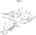
- Fig. 1 is an exploded perspective view illustrating a schematic structure of a protection circuit unit according to the first embodiment.
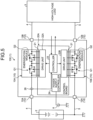
- Fig. 2 is a circuit diagram illustrating a schematic structure of the protection circuit unit according to the first embodiment.
- Fig. 3 is a perspective view illustrating a schematic structure of an energization module according to the first embodiment.
- Fig. 1 illustrates a state before the energization module is attached to the control board.
- Fig. 3 illustrates a resin mold member in the energization module with broken lines.
- a protection circuit unit 1 is mounted on a vehicle, such as an electric vehicle (EV), a hybrid electric vehicle (HEV), and a plug-in hybrid electric vehicle (PHEV). As illustrated in Fig. 2 , the protection circuit unit 1 is disposed on an electric path 4 between a high-voltage battery 2 of the vehicle and a high-voltage load 3 receiving supply of power from the high-voltage battery 2, and opens and closes the electric path 4 on the basis of an energization current of the electric path 4.
- the terms “open” and “close” of the electric path 4 mean “energization” and "shutoff" of the electric path 4. In the following explanation, electric connection is simply referred to as “connection”, and electric shutoff is simply referred to as "shutoff”.
- the protection circuit unit 1 shuts off the electric path 4, for example, when the energization current value flowing through the electric path 4 exceeds a threshold.
- the threshold is an upper limit value of the energization current value set to protect semiconductor switches Q1 and Q2 in the protection circuit unit 1, the high-voltage battery 2, the high-voltage load 3, and electric wires forming the electric path 4, and the like.
- the protection circuit unit 1 mainly includes an energization module 10 and a control board 20, as illustrated in Fig. 1 and Fig. 2 .
- the high-voltage battery 2 is a high-voltage power supply to drive the high-voltage load 3 mounted on the vehicle.
- the high-voltage battery 2 has a voltage, for example, higher than 12 V (or 24 V), and outputs direct-current power.
- the high-voltage battery 2 is, for example, a battery pack in which a plurality of battery cells are connected.
- the high-voltage battery 2 is connected at a positive electrode side with an input terminal of the protection circuit unit 1, and grounded at a negative electrode side.
- the high-voltage battery 2 may have different specifications, for example, according to the model of the vehicle.
- the high-voltage battery 2 is not limited to a battery pack, but may be of any form, as long as it is capable of supplying direct-current power.
- the high-voltage load 3 is driven with direct-current power supplied from the high-voltage battery 2.
- the high-voltage load 3 is a driving motor or the like mounted on the vehicle.
- the high-voltage load 3 is connected at a positive electrode side with an output terminal of the protection circuit unit 1, and grounded at a negative electrode side.
- the high-voltage load 3 may have different specifications, for example, according to the model of the vehicle.
- the energization module 10 is disposed on the electric path 4 between the high-voltage battery 2 and the high-voltage load 3 supplied with power from the high-voltage battery 2, and opens and closes the electric path 4.
- the energization module 10 includes the semiconductor switches Q1 and Q2, bus bars 12A, 12B, and 12C, a control terminal 13, and a resin mold member 14.
- the energization module 10 is configured to be a member separated from the control board 20 and replaceable, and a plurality of types of the energization modules 10 are prepared in accordance with the energization current values of the electric path 4.
- the energization module 10 may have different specifications for the bus bars 12A to 12C and/or the semiconductor switches Q1 and Q2 in accordance with the energization current values of the electric path 4.
- the control terminal 13 is an element connected with the semiconductor switches Q1 and Q2 and supplied with signals from outside to control the semiconductor switches Q1 and Q2.
- the control terminal 13 functions as a connection terminal connecting the semiconductor switches Q1 and Q2 with the control board 20.
- the control terminal 13 includes, for example, five pin terminals common to a plurality of types of the energization modules 10.
- the five pin terminals are formed of, for example, a metal member having electric conductivity, and arranged at regular intervals. Each of the pins is formed to extend in a direction orthogonal to the extending direction of the bus bar 12, project from the resin mold member 14, and be bent toward the control board 20 in a state in which the energization module 10 is mounted on the control board 20.
- the control terminal 13 is mounted on a surface reverse to a mount surface 20a of the control board 20 by soldering or the like, and electrically connected with the control circuit on the control board 20.
- the resin mold member 14 is molded from, for example, a synthetic resin having insulating property and thermal conductivity, to cover the semiconductor switches Q1 and Q2. As illustrated in Fig. 3 , the resin mold member 14 contains the whole semiconductor switches Q1 and Q2, the whole bonding wires 15, part of the control terminal 13, and part of the bus bar 12. The resin mold member 14 forms the semiconductor switches Q1 and Q2, the bus bar 12, the control terminal 13, and the bonding wires 15 as one unitary piece.
- the resin mold member 14 includes a heat radiation surface 14a of the energization module 10. For example, the heat radiation surface 14a is configured to be exposed to the outside as a heat radiation element of the energization module 10, but the structure is not limited thereto.
- the heat radiation surface 14a may be a part to which a heat radiation member (heat sink) is attached, or a part attached to a housing containing the energization module 10.
- the energization module 10 includes the heat radiation surface 14a on a side reverse to the mount surface 20a of the control board 20, in a state in which the energization module 10 is mounted on the control board 20.
- the control board 20 is configured as a member separated from the energization module 10 and electrically connected with the energization module 10, to control opening/closing of the electric path on the basis of the energization current flowing through the electric path 4.
- the control board 20 forms a control circuit mainly formed of a microcomputer.
- a plurality of electronic components 25 are mounted on the mount surface 20a, and the energization module 10 is mounted on a side reverse to the mount surface 20a.
- the control board 20 is electrically connected with an electric control unit (ECU) (not illustrated) or the like in the vehicle, to transmit and receive signals to and from the ECU.
- ECU electric control unit
- the control board 20 according to the present embodiment includes a connection unit 21, a drive unit 22, and a controller 23.
- the connection unit 21 is a connecting unit corresponding to the control terminal 13 of each of a plurality of types of the energization modules 10 and connecting the energization module 10 with the control board 20.
- the connection unit 21 includes a plurality of through holes 20b provided on the control board 20 at intervals equal to those of the pin terminals, to correspond to the control terminal 13 including the pin terminals arranged at regular intervals.
- the connection unit 21 includes, for example, five through holes 20b to correspond to five pin terminals common to control terminals 13 of a plurality of types of the energization modules 10.
- the control terminal 13 of the energization module 10 is soldered to the through holes 20b.
- the drive unit 22 is a drive circuit driving the semiconductor switches Q1 and Q2.
- the drive unit 22 outputs a drive signal to the semiconductor switches Q1 and Q2 connected with the connection unit 21, in response to a control signal from the controller 23.
- Each of the semiconductor switches Q1 and Q2 is changed to an on state in response to the drive signal, and the high-voltage battery 2 and the high-voltage load 3 are connected.
- the controller 23 outputs a control signal to control driving of the energization module 10 to the drive unit 22.
- the control signal is, for example, a signal to perform energization and shutoff of the electric path 4 with the semiconductor switches Q1 and Q2.
- the controller 23 may be configured to output a control signal to the drive unit 22 on the basis of a signal input from an external ECU or the like.
- the controller 23 recognizes the open/close state of the semiconductor switches Q1 and Q2, to determine whether the electric path 4 is energized.
- the controller 23 acquires an energization current value detected with a current sensor (not illustrated) in a state in which the electric path 4 is energized.
- the controller 23 determines whether the energization current value exceeds the threshold, and outputs a control signal to the drive unit 22 when the energization current value exceeds the threshold.
- the drive unit 22 stops output of the drive signal to the semiconductor switches Q1 and Q2 in response to the control signal received from the controller 23. In this manner, each of the semiconductor switches Q1 and Q2 is changed to the off state, and the electric path 4 is shut off.
- the protection circuit unit 1 includes the energization module 10 disposed on the electric path 4 between the high-voltage battery 2 of the vehicle and the high-voltage load 3 receiving supply of power from the high-voltage battery 2, and opening/closing the electric path 4, and the control board 20 configured separately from the energization module 10, electrically connected with the energization module 10, and controlling opening/closing of the electric path 4 on the basis of the energization current flowing through the electric path 4.
- the energization module 10 includes the semiconductor switches Q1 and Q2 opening and closing the electric path 4, a bus bar 12 connected at one end with the high-voltage battery 2 side and connected at the other end with the high-voltage load 3 side with the semiconductor switches Q1 and Q2 interposed therebetween, and the control terminal 13 connected the semiconductor switches Q1 and Q2 with the control board 20.
- the control board 20 includes the connection unit 21 corresponding to each of control terminals 13 of a plurality of types of the energization modules 10.
- a vehicle power supply device 100 according to the second embodiment is different from the protection circuit unit 1 according to the first embodiment described above, in that two energization modules 10A and 10B are electrically connected with a control board 20A.
- constituent elements equal to those in the first embodiment are denoted by the same reference numerals as those in the first embodiment, and an explanation thereof is omitted.
- the vehicle power supply device 100 is mounted on a vehicle, such as an electric vehicle (EV), a hybrid electric vehicle (HEV), and a plug-in hybrid electric vehicle (PHEV), like the protection circuit unit 1 described above. As illustrated in Fig. 5 , the vehicle power supply device 1 is disposed on electric paths 4 and 5 between a high-voltage battery 2 of the vehicle and a high-voltage load 3 receiving supply of power from the high-voltage battery 2, to open and close each of the electric paths 4 and 5.
- a vehicle such as an electric vehicle (EV), a hybrid electric vehicle (HEV), and a plug-in hybrid electric vehicle (PHEV), like the protection circuit unit 1 described above.
- EV electric vehicle
- HEV hybrid electric vehicle
- PHEV plug-in hybrid electric vehicle
- the vehicle power supply device 100 shuts off the electric paths 4 and 5, to protect semiconductor switches Q1 and Q2 in the vehicle power supply device 100, the high-voltage battery 2, the high-voltage load 3, and electric wires forming the electric paths 4 and 5, when the energization current value flowing through the electric paths 4 and 5 exceeds the threshold.
- the vehicle power supply device 100 includes a protection circuit unit 1 and a housing 7 containing the energization modules 10A and 10B and the control board 20A forming the protection circuit unit 1.
- the controller 23 outputs a control signal to control driving of the energization modules 10A and 10B to the drive units 22A and 22B.
- the control signal is a signal to perform energization and shutoff of the electric paths 4 and 5 with, for example, the semiconductor switches Q1 and Q2.
- the controller 23 may be configured to output a control signal to the drive units 22A and 22B on the basis of a signal input from an external ECU or the like.
- the housing 7 is formed of an upper cover 8 and a lower cover 9, as illustrated in Fig. 4 .
- the upper cover 8 and the lower cover 9 are formed of a synthetic resin or the like having insulating property.
- the lower cover 9 includes two openings 9a communicating with the outside.
- the energization modules 10A and 10B have a structure in which the heat radiation surfaces 16a of their housings 16 face the openings 9a, in a state in which the energization modules 10A and 10B are mounted on the control board 20A.
- the structure described above produces similar effect to that of the first embodiment described above, and improves the heat radiation effect by exposing the heat radiation surfaces 16a of the energization modules 10A and 10B at high temperature in energization to the outside of the housing 7 and the external air.
- this structure enables handling of the energization modules 10A and 10B with one control board 20A, and enables reduction in cost by reduction in number of components.
- this structure enables compatibility with a plurality of vehicle models by changing only the heat radiation members attached to the heat radiation surfaces 16a, without changing the control board 20A or the energization module 10A and 10B.
- energization modules 10, 10A, and 10B are formed with the resin mold member 14 or the housing 16, but the structure is not limited thereto.
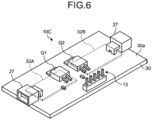
- Fig. 6 is a perspective view illustrating a schematic structure of an energization module according to a modification of the first and the second embodiments.
- An energization module 10C in the modification of the present embodiment is different from the first and the second embodiments, in that the energization module 10C is formed of a thick copper board 30 in which a pair of bus bars 32A and 32B are formed as inner layers.
- each of the semiconductor switches Q1 and Q2 is formed of a power MOS-FET, but the structure is not limited thereto.
- each of the semiconductor switches Q1 and Q2 may be formed of a transistor and/or an insulated gate bipolar transistor (IGBT) or the like.
- each of the energization modules 10, 10A, and 10B includes a pair of semiconductor switches Q1 and Q2, but the structure is not limited thereto.
- a semiconductor switch may be used, as long as the semiconductor switch has the same function as those of the semiconductor switches Q1 and Q2.
- each of the energization modules 10, 10A, and 10B may have a structure of including a semiconductor switch Q1 to open and close the electric paths 4 and 5 between the high-voltage battery 2 and the high-voltage load 3.
Landscapes
- Engineering & Computer Science (AREA)
- Power Engineering (AREA)
- Mechanical Engineering (AREA)
- Transportation (AREA)
- Life Sciences & Earth Sciences (AREA)
- Sustainable Development (AREA)
- Sustainable Energy (AREA)
- Microelectronics & Electronic Packaging (AREA)
- Battery Mounting, Suspending (AREA)
- Continuous-Control Power Sources That Use Transistors (AREA)
- Charge And Discharge Circuits For Batteries Or The Like (AREA)
- Protection Of Static Devices (AREA)
Description
- The present invention relates to a vehicle power supply device.
- Some vehicles, such as electric vehicles (EV) and plug-in hybrid electric vehicles (PHEV), include vehicle power supply devices disposed on an electric path supplying power from a high-voltage battery to a load, such as a motor. Vehicle power supply devices have a current shutoff function for the purpose of protecting the load and/or electric wires forming the electric path. Each of the vehicle power supply devices includes, for example, a semiconductor relay opening and closing the electric path, and a drive circuit driving the semiconductor relay, and they are mounted on a control board. For this reason, the current flowing from the high-voltage battery to the load flows through the electric path on the control board. When the current increases, it is required to increase the area of the wiring pattern and/or the thickness of the copper foil on the control board. For this reason, an electronic circuit structure has been proposed (for example, see Patent Literature 1:
Japanese Patent Application Laid-open No. 2016-12591 - In the prior art described above, there are cases where the control board is difficult to miniaturize because a space to mount the bus bar is required on the control board. In addition, when the current flowing through the electric path on the control board is changed in accordance with change in specifications of the high-voltage battery and/or the load mounted on the vehicle, a new design is required for the bus bar and the board to mount the bus bar, and there is room for improvement in respect of a cost.
- Further prior art is known from
documents EP 1 203 698 A2 ,JP 2016 220276 A US 2017/186572 A1 ,DE 10 2011 056270 A1EP 1 956 649 A2 ,US 2007/096278 A1 andUS 2011/221 268 A1 . - An object of the present invention is to provide a vehicle power supply device enabling miniaturization of a control board at a low cost.
- This object is solved by the subject matter of
claim 1. - The above and other objects, features, advantages and technical and industrial significance of this invention will be better understood by reading the following detailed description of presently preferred embodiments of the invention, when considered in connection with the accompanying drawings.
-
-
Fig. 1 is an exploded perspective view illustrating a schematic structure of a protection circuit unit according to a first embodiment; -
Fig. 2 is a circuit diagram illustrating a schematic structure of the protection circuit unit according to the first embodiment; -
Fig. 3 is a perspective view illustrating a schematic structure of an energization module according to the first embodiment; -
Fig. 4 is an exploded perspective view illustrating a schematic structure of a vehicle power supply device according to a second embodiment; -
Fig. 5 is a circuit diagram illustrating a schematic structure of the vehicle power supply device according to the second embodiment; and -
Fig. 6 is a perspective view illustrating a schematic structure of an energization module according to a modification of the first and the second embodiments. - The following is a detailed explanation of a protection circuit unit and a vehicle power supply device according to embodiments of the present invention with reference to drawings. The present invention is not limited to the following embodiments. Constituent elements in the following embodiments include ones that the skilled person in the art could easily expect or substantially the same ones. In addition, the structures described hereinafter may be properly used in combination.
- The following is an explanation of a protection circuit unit according to the first embodiment of the present invention with reference to
Fig. 1 to Fig. 3 .Fig. 1 is an exploded perspective view illustrating a schematic structure of a protection circuit unit according to the first embodiment.Fig. 2 is a circuit diagram illustrating a schematic structure of the protection circuit unit according to the first embodiment.Fig. 3 is a perspective view illustrating a schematic structure of an energization module according to the first embodiment.Fig. 1 illustrates a state before the energization module is attached to the control board.Fig. 3 illustrates a resin mold member in the energization module with broken lines. - A
protection circuit unit 1 is mounted on a vehicle, such as an electric vehicle (EV), a hybrid electric vehicle (HEV), and a plug-in hybrid electric vehicle (PHEV). As illustrated inFig. 2 , theprotection circuit unit 1 is disposed on anelectric path 4 between a high-voltage battery 2 of the vehicle and a high-voltage load 3 receiving supply of power from the high-voltage battery 2, and opens and closes theelectric path 4 on the basis of an energization current of theelectric path 4. The terms "open" and "close" of theelectric path 4 mean "energization" and "shutoff" of theelectric path 4. In the following explanation, electric connection is simply referred to as "connection", and electric shutoff is simply referred to as "shutoff". Theprotection circuit unit 1 according to the present embodiment shuts off theelectric path 4, for example, when the energization current value flowing through theelectric path 4 exceeds a threshold. The threshold is an upper limit value of the energization current value set to protect semiconductor switches Q1 and Q2 in theprotection circuit unit 1, the high-voltage battery 2, the high-voltage load 3, and electric wires forming theelectric path 4, and the like. Theprotection circuit unit 1 mainly includes anenergization module 10 and acontrol board 20, as illustrated inFig. 1 andFig. 2 . - The high-
voltage battery 2 is a high-voltage power supply to drive the high-voltage load 3 mounted on the vehicle. The high-voltage battery 2 has a voltage, for example, higher than 12 V (or 24 V), and outputs direct-current power. The high-voltage battery 2 is, for example, a battery pack in which a plurality of battery cells are connected. The high-voltage battery 2 is connected at a positive electrode side with an input terminal of theprotection circuit unit 1, and grounded at a negative electrode side. The high-voltage battery 2 may have different specifications, for example, according to the model of the vehicle. The high-voltage battery 2 is not limited to a battery pack, but may be of any form, as long as it is capable of supplying direct-current power. - The high-
voltage load 3 is driven with direct-current power supplied from the high-voltage battery 2. For example, the high-voltage load 3 is a driving motor or the like mounted on the vehicle. The high-voltage load 3 is connected at a positive electrode side with an output terminal of theprotection circuit unit 1, and grounded at a negative electrode side. The high-voltage load 3 may have different specifications, for example, according to the model of the vehicle. - The
energization module 10 is disposed on theelectric path 4 between the high-voltage battery 2 and the high-voltage load 3 supplied with power from the high-voltage battery 2, and opens and closes theelectric path 4. As illustrated inFig. 3 , theenergization module 10 includes the semiconductor switches Q1 and Q2,bus bars control terminal 13, and aresin mold member 14. Theenergization module 10 is configured to be a member separated from thecontrol board 20 and replaceable, and a plurality of types of theenergization modules 10 are prepared in accordance with the energization current values of theelectric path 4. For example, theenergization module 10 may have different specifications for thebus bars 12A to 12C and/or the semiconductor switches Q1 and Q2 in accordance with the energization current values of theelectric path 4. - The semiconductor switches Q1 and Q2 are arranged in the
electric path 4, to open and close theelectric path 4. Each of the semiconductor switches Q1 and Q2 is formed of, for example, a power metal-oxide-semiconductor field-effect-transistor (MOS-FET) serving as a type of field-effect-transistors. As illustrated inFig. 2 , the semiconductor switches Q1 and Q2 are connected in series with theelectric path 4 such that the forward directions of their parasitic diodes are reversed, to open and close theelectric path 4. The semiconductor switch Q1 is, for example, an N-channel MOS-FET. The semiconductor switch Q2 is, for example, an N-channel MOS-FET. In theenergization module 10, the flow of the power between the high-voltage battery 2 and the high-voltage load 3 is shut off, when both of the semiconductor switches Q1 and Q2 are in the off state. As illustrated inFig. 3 , each of the semiconductor switches Q1 and Q2 according to the present embodiment is formed in a state of a bare chip, and disposed on a lead frame (for example, the bus bar 12) through which the energization current flows. - As illustrated in
Fig. 2 , thebus bars 12A (12), 12B (12), and 12C (12) are connected at one side with the high-voltage battery 2 side, and connected at the other end with the high-voltage load 3 side, with the semiconductor switches Q1 and Q2 interposed therebetween. Each of the bus bars 12A to 12C serves as a conductive member forming part of theelectric path 4, and is formed of a metal material, such as copper alloy. Each of thebus bars bus bar 12A forms the input-side terminal and thebus bar 12B forms the output-side terminal, thebus bar 12A is connected with the high-voltage battery 2 via theelectric path 4, and thebus bar 12B is connected with the high-voltage load 3 through theelectric path 4. As illustrated inFig. 3 , thebus bar 12A and thebus bar 12B are connected with each other via the semiconductor switch Q1, thebus bar 12C, and the semiconductor switch Q2, and aresin mold member 14 is formed to protect the semiconductor switches Q1 and Q2. The semiconductor switch Q1 is connected with one end portion in the extending direction of thebus bar 12A, and connected with thebus bar 12C via a plurality ofbonding wires 15. The semiconductor switch Q2 is connected with the other end portion in the extending direction of thebus bar 12B, and connected with thebus bar 12C via a plurality ofbonding wires 15. Thebus bar 12A is connected with thecontrol terminal 13 through abonding wire 17. Thebus bar 12B is connected with thecontrol terminal 13 through abonding wire 17. Thebus bar 12C is connected with thecontrol terminal 13 through abonding wire 17. The semiconductor switches Q1 and Q2 are connected with thecontrol terminal 13 throughbonding wires 17. - The
control terminal 13 is an element connected with the semiconductor switches Q1 and Q2 and supplied with signals from outside to control the semiconductor switches Q1 and Q2. Thecontrol terminal 13 according to the present embodiment functions as a connection terminal connecting the semiconductor switches Q1 and Q2 with thecontrol board 20. Thecontrol terminal 13 includes, for example, five pin terminals common to a plurality of types of theenergization modules 10. The five pin terminals are formed of, for example, a metal member having electric conductivity, and arranged at regular intervals. Each of the pins is formed to extend in a direction orthogonal to the extending direction of thebus bar 12, project from theresin mold member 14, and be bent toward thecontrol board 20 in a state in which theenergization module 10 is mounted on thecontrol board 20. Thecontrol terminal 13 is mounted on a surface reverse to amount surface 20a of thecontrol board 20 by soldering or the like, and electrically connected with the control circuit on thecontrol board 20. - The
resin mold member 14 is molded from, for example, a synthetic resin having insulating property and thermal conductivity, to cover the semiconductor switches Q1 and Q2. As illustrated inFig. 3 , theresin mold member 14 contains the whole semiconductor switches Q1 and Q2, thewhole bonding wires 15, part of thecontrol terminal 13, and part of thebus bar 12. Theresin mold member 14 forms the semiconductor switches Q1 and Q2, thebus bar 12, thecontrol terminal 13, and thebonding wires 15 as one unitary piece. Theresin mold member 14 includes aheat radiation surface 14a of theenergization module 10. For example, theheat radiation surface 14a is configured to be exposed to the outside as a heat radiation element of theenergization module 10, but the structure is not limited thereto. For example, theheat radiation surface 14a may be a part to which a heat radiation member (heat sink) is attached, or a part attached to a housing containing theenergization module 10. Theenergization module 10 includes theheat radiation surface 14a on a side reverse to themount surface 20a of thecontrol board 20, in a state in which theenergization module 10 is mounted on thecontrol board 20. - The
control board 20 is configured as a member separated from theenergization module 10 and electrically connected with theenergization module 10, to control opening/closing of the electric path on the basis of the energization current flowing through theelectric path 4. Thecontrol board 20 forms a control circuit mainly formed of a microcomputer. In thecontrol board 20, a plurality ofelectronic components 25 are mounted on themount surface 20a, and theenergization module 10 is mounted on a side reverse to themount surface 20a. Thecontrol board 20 is electrically connected with an electric control unit (ECU) (not illustrated) or the like in the vehicle, to transmit and receive signals to and from the ECU. Thecontrol board 20 according to the present embodiment includes aconnection unit 21, adrive unit 22, and acontroller 23. - The
connection unit 21 is a connecting unit corresponding to thecontrol terminal 13 of each of a plurality of types of theenergization modules 10 and connecting theenergization module 10 with thecontrol board 20. For example, theconnection unit 21 includes a plurality of throughholes 20b provided on thecontrol board 20 at intervals equal to those of the pin terminals, to correspond to thecontrol terminal 13 including the pin terminals arranged at regular intervals. Theconnection unit 21 includes, for example, five throughholes 20b to correspond to five pin terminals common to controlterminals 13 of a plurality of types of theenergization modules 10. Thecontrol terminal 13 of theenergization module 10 is soldered to the throughholes 20b. - The
drive unit 22 is a drive circuit driving the semiconductor switches Q1 and Q2. Thedrive unit 22 outputs a drive signal to the semiconductor switches Q1 and Q2 connected with theconnection unit 21, in response to a control signal from thecontroller 23. Each of the semiconductor switches Q1 and Q2 is changed to an on state in response to the drive signal, and the high-voltage battery 2 and the high-voltage load 3 are connected. - The
controller 23 outputs a control signal to control driving of theenergization module 10 to thedrive unit 22. The control signal is, for example, a signal to perform energization and shutoff of theelectric path 4 with the semiconductor switches Q1 and Q2. Thecontroller 23 may be configured to output a control signal to thedrive unit 22 on the basis of a signal input from an external ECU or the like. - The following is an explanation of an example of energization and shutoff operations of the
protection circuit unit 1 according to the present embodiment. Thecontroller 23 recognizes the open/close state of the semiconductor switches Q1 and Q2, to determine whether theelectric path 4 is energized. Thecontroller 23 acquires an energization current value detected with a current sensor (not illustrated) in a state in which theelectric path 4 is energized. Thecontroller 23 determines whether the energization current value exceeds the threshold, and outputs a control signal to thedrive unit 22 when the energization current value exceeds the threshold. Thedrive unit 22 stops output of the drive signal to the semiconductor switches Q1 and Q2 in response to the control signal received from thecontroller 23. In this manner, each of the semiconductor switches Q1 and Q2 is changed to the off state, and theelectric path 4 is shut off. - As explained above, the
protection circuit unit 1 according to the present embodiment includes theenergization module 10 disposed on theelectric path 4 between the high-voltage battery 2 of the vehicle and the high-voltage load 3 receiving supply of power from the high-voltage battery 2, and opening/closing theelectric path 4, and thecontrol board 20 configured separately from theenergization module 10, electrically connected with theenergization module 10, and controlling opening/closing of theelectric path 4 on the basis of the energization current flowing through theelectric path 4. Theenergization module 10 includes the semiconductor switches Q1 and Q2 opening and closing theelectric path 4, abus bar 12 connected at one end with the high-voltage battery 2 side and connected at the other end with the high-voltage load 3 side with the semiconductor switches Q1 and Q2 interposed therebetween, and thecontrol terminal 13 connected the semiconductor switches Q1 and Q2 with thecontrol board 20. Thecontrol board 20 includes theconnection unit 21 corresponding to each ofcontrol terminals 13 of a plurality of types of theenergization modules 10. - The structure described above removes the necessity for flowing the high-voltage energization current flowing from the high-
voltage battery 2 to the high-voltage load 3 through thecontrol board 20, and the necessity for the space to mount thebus bar 12 on the control board. This structure enables easy miniaturization of thecontrol board 20. In addition, because no high-voltage energization current flows through thecontrol board 20, this structure removes the necessity for using an expensive thick copper board or a metal core board for thecontrol board 20, and enables manufacturing of thecontrol board 20 at a low cost. Besides, for example, even when the energization current flowing through theelectric path 4 differs due to the difference in vehicle model, this structure enables compatibility with a plurality of vehicle models by changing only theenergization module 10, without changing thecontrol board 20. - The following is an explanation of a vehicle power supply device according to a second embodiment of the present invention, with reference to
Fig. 4 andFig. 5 .Fig. 4 is an exploded perspective view illustrating a schematic structure of a vehicle power supply device according to the second embodiment.Fig. 5 is a circuit diagram illustrating a schematic structure of the vehicle power supply device according to the second embodiment. - A vehicle
power supply device 100 according to the second embodiment is different from theprotection circuit unit 1 according to the first embodiment described above, in that twoenergization modules control board 20A. In the following explanation, constituent elements equal to those in the first embodiment are denoted by the same reference numerals as those in the first embodiment, and an explanation thereof is omitted. - The vehicle
power supply device 100 is mounted on a vehicle, such as an electric vehicle (EV), a hybrid electric vehicle (HEV), and a plug-in hybrid electric vehicle (PHEV), like theprotection circuit unit 1 described above. As illustrated inFig. 5 , the vehiclepower supply device 1 is disposed onelectric paths voltage battery 2 of the vehicle and a high-voltage load 3 receiving supply of power from the high-voltage battery 2, to open and close each of theelectric paths power supply device 100 shuts off theelectric paths power supply device 100, the high-voltage battery 2, the high-voltage load 3, and electric wires forming theelectric paths electric paths Fig. 4 , the vehiclepower supply device 100 includes aprotection circuit unit 1 and ahousing 7 containing theenergization modules control board 20A forming theprotection circuit unit 1. - The
energization module 10A is disposed on the positive-electrode-sideelectric path 4 between the high-voltage battery 2 and the high-voltage load 3 receiving supply of power from the high-voltage battery 2, to open and close theelectric path 4. Theenergization module 10B is disposed on the negative-electrode-sideelectric path 5 between the high-voltage battery 2 and the high-voltage load 3 receiving supply of power from the high-voltage battery 2, to open and close theelectric path 5. As illustrated inFig. 5 , each of theenergization modules bus bar 12, a plurality ofcontrol terminals 13, and ahousing 16. Each of theenergization modules control board 20A and replaceable, and a plurality of types of theenergization modules electric paths energization modules bus bars electric paths - The
housing 16 is molded from, for example, a synthetic resin having insulating property and thermal conductivity, to cover the whole semiconductor switches Q1 and Q2, thewhole bonding wires 15, part of thecontrol terminals 13, and part of thebus bar 12. Thehousing 16 includes heat radiation surfaces 16a of theindividual energization modules housing 7 as elements for heat radiation of theenergization modules 10, but the structure is not limited thereto. For example, theheat radiation surfaces 16a may be parts to which heat radiation members are attached, or parts attached to thehousing 7. Theindividual energization modules mount surface 20a of thecontrol board 20A, in a state in which theenergization modules control board 20A. - The
control board 20A is configured as a member separated from theenergization modules energization modules electric paths electric paths control board 20A forms a control circuit mainly formed of a microcomputer. In thecontrol board 20A, theenergization modules mount surface 20a. Thecontrol board 20A is electrically connected with an electric control unit (ECU) (not illustrated) or the like in the vehicle, to transmit and receive signals to and from the ECU. Thecontrol board 20A according to the present embodiment includes aconnection unit 21, twodrive units controller 23, apower supply controller 24, and acurrent sensor 26. - The
controller 23 according to the present embodiment outputs a control signal to control driving of theenergization modules drive units electric paths controller 23 may be configured to output a control signal to thedrive units - The
power supply controller 24 is connected with a 12V battery 6 in the vehicle, to convert a direct-current voltage acquired from the 12V battery 6 into drive voltages of the individual units and apply the voltages to thecontroller 23 and thedrive units - The
current sensor 26 is a detector detecting the energization current of the electric path 4 (or electric path 5). Thecurrent sensor 26 is connected with thecontroller 23, and a detection value detected with thecurrent sensor 26 is output to thecontroller 23. - The
housing 7 is formed of an upper cover 8 and alower cover 9, as illustrated inFig. 4 . The upper cover 8 and thelower cover 9 are formed of a synthetic resin or the like having insulating property. Thelower cover 9 includes twoopenings 9a communicating with the outside. Theenergization modules housings 16 face theopenings 9a, in a state in which theenergization modules control board 20A. - The following is an explanation of an example of energization and shutoff operations of the vehicle
power supply device 100 according to the present embodiment. Thecontroller 23 determines, with thecurrent sensor 26, whether theelectric path 4 is energized. Thecontroller 23 acquires the energization current value detected with thecurrent sensor 26 in the state in which theelectric path 4 is energized. Thecontroller 23 determines whether the energization current value exceeds the threshold, and outputs a control signal to thedrive unit 22A when the energization current value exceeds the threshold. Thedrive unit 22A stops output of the drive signal to the semiconductor switches Q1 and Q2 of theenergization module 10A in response to the control signal received from thecontroller 23. In this manner, each of the semiconductor switches Q1 and Q2 is changed to the off state, and theelectric path 4 is shut off. - As explained above, the vehicle
power supply device 100 according to the present embodiment includes theprotection circuit unit 1 and thehousing 7 containing theenergization modules control board 20A forming theprotection circuit unit 1. Thehousing 7 includesopenings 9a communicating with the outside. Theenergization modules heat radiation surface 16a on a side reverse to themount surface 20a of thecontrol board 20A in the state in which theenergization modules control board 20A. Theheat radiation surface 16a faces theopening 9a of thehousing 7. - The structure described above produces similar effect to that of the first embodiment described above, and improves the heat radiation effect by exposing the heat radiation surfaces 16a of the
energization modules housing 7 and the external air. In addition, this structure enables handling of theenergization modules control board 20A, and enables reduction in cost by reduction in number of components. In addition, when the energization current flowing through theelectric paths heat radiation surfaces 16a, without changing thecontrol board 20A or theenergization module - In the first and the second embodiments described above, the
energization modules resin mold member 14 or thehousing 16, but the structure is not limited thereto.Fig. 6 is a perspective view illustrating a schematic structure of an energization module according to a modification of the first and the second embodiments. Anenergization module 10C in the modification of the present embodiment is different from the first and the second embodiments, in that theenergization module 10C is formed of athick copper board 30 in which a pair ofbus bars - The
thick copper board 30 includes amount surface 30a. A pair of semiconductor switches Q1 and Q2, twoconnectors 27, and acontrol terminal 13 are mounted on themount surface 30a. Thethick copper board 30 includes a pair ofbus bars mount surface 30a. One of the twoconnectors 27 is connected with thebus bar 32A, and the other is connected with thebus bar 32B. One of the twoconnectors 27 is an input terminal and the other is an output terminal. One of the twoconnectors 27 is connected with the high-voltage battery 2, and the other is connected with the high-voltage load 3. Because the input terminal and the output terminal are formed as members separated from the bus bars, this structure enables easy compatibility even when the specifications of thethick copper board 30 are changed. In addition, because the input terminal and the output terminal are formed as connectors, this structure improves workability in assembly of theenergization module 10C. - The bus bars 32A and 32B are connected with each other via the semiconductor switches Q1 and Q2 mounted on the
mount surface 30a of thethick copper board 30. Because thebus bars thick copper board 30, this structure enables miniaturization of the energization module itself. - In the first and the second embodiments, each of the semiconductor switches Q1 and Q2 is formed of a power MOS-FET, but the structure is not limited thereto. For example, each of the semiconductor switches Q1 and Q2 may be formed of a transistor and/or an insulated gate bipolar transistor (IGBT) or the like.
- In addition, in the first and the second embodiments, each of the
energization modules energization modules electric paths voltage battery 2 and the high-voltage load 3. - In the first and the second embodiments, the
connection unit 21 includes three throughholes 20b to correspond to three pin terminals common to thecontrol terminals 13 of a plurality of types of theenergization modules 10, but the structure is not limited thereto. For example, when the maximum number of pin terminals of thecontrol terminal 13 is five in a plurality of types of theenergization modules 10, theconnection unit 21 may include at least five throughholes 20b to correspond to the five pin terminals. In addition, theconnection unit 21 includes a plurality of throughholes 20b to correspond to the pin terminals forming thecontrol terminal 13 of theenergization module 10, but the structure is not limited thereto. Theconnection unit 21 may have a connection form in which connectors are connected. - The protection circuit unit and the vehicle power supply device according to the present embodiment produce the effect of enabling miniaturization of a control board at a low cost.
Claims (1)
- A vehicle power supply device (100) comprising:
a protection circuit unit (1) comprising:at least one energization module (10, 10A-10C) configured to be disposed on an electric path (4, 5) between a power supply (2) of a vehicle and a load (3) receiving supply of power from the power supply (2), to open and close the electric path (4, 5); anda control board (20, 20A) configured to be a member separated from the energization module (10, 10A-10C) and electrically connected with the energization module (10, 10A-10C), to control opening and closing of the electric path (4, 5) on the basis of an energization current flowing through the electric path (4, 5), whereinthe energization module (10, 10A-10C) includes:at least one semiconductor switch (Q1, Q2) opening and closing the electric path (4, 5);a bus bar (12, 12A, 12B, 32A, 32B) connected at one end with the power supply (2) side and connected at the other end with the load (3) side, with the semiconductor switch (Q1, Q2) interposed therebetween; anda control terminal (13) connecting the semiconductor switch (Q1, Q2) with the control board (20, 20A),the control board (20, 20A) includes a connection unit (21) corresponding to the control terminal (13) of each of a plurality of types of the energization modules (10, 10A-10C),characterized in thatthe control board (20, 20A) has a mount surface (20a) on which a plurality of electronic components (25) are mounted,the energization module (10, 10A-10C) is mounted on a surface of an opposite side to the mounting surface (20a) in the control board (20, 20A), anda housing (7) containing the energization module (10, 10A-10C) and the control board (20, 20A) forming the protection circuit unit (1), whereinthe housing (7) includes an opening (9a) communicating with outside,the energization module (10, 10A-10C) includes a heat radiation surface (14a, 16a) on a side reverse to a mount surface (20a) of the control board (20, 20A) in a state in which the energization module (10, 10A-10C) is mounted on the control board (20, 20A), and the heat radiation surface (14a, 16a) faces the opening (9a).
Applications Claiming Priority (1)
| Application Number | Priority Date | Filing Date | Title |
|---|---|---|---|
| JP2019009037A JP6926132B2 (en) | 2019-01-23 | 2019-01-23 | Protection circuit unit and vehicle power supply |
Publications (2)
| Publication Number | Publication Date |
|---|---|
| EP3687026A1 EP3687026A1 (en) | 2020-07-29 |
| EP3687026B1 true EP3687026B1 (en) | 2023-08-02 |
Family
ID=69105679
Family Applications (1)
| Application Number | Title | Priority Date | Filing Date |
|---|---|---|---|
| EP19215968.9A Active EP3687026B1 (en) | 2019-01-23 | 2019-12-13 | Vehicle power supply device |
Country Status (4)
| Country | Link |
|---|---|
| US (1) | US11241966B2 (en) |
| EP (1) | EP3687026B1 (en) |
| JP (1) | JP6926132B2 (en) |
| CN (1) | CN111497618B (en) |
Families Citing this family (1)
| Publication number | Priority date | Publication date | Assignee | Title |
|---|---|---|---|---|
| CN113286420A (en) * | 2020-10-28 | 2021-08-20 | 华为技术有限公司 | Circuit bearing plate, power distribution unit and equipment |
Citations (4)
| Publication number | Priority date | Publication date | Assignee | Title |
|---|---|---|---|---|
| US20070096278A1 (en) * | 2005-08-19 | 2007-05-03 | Hitachi, Ltd. | Semiconductor unit, and power conversion system and on-vehicle electrical system using the same |
| EP1956649A2 (en) * | 2007-02-07 | 2008-08-13 | Hitachi, Ltd. | Power conversion apparatus |
| US20110221268A1 (en) * | 2008-10-23 | 2011-09-15 | Hitachi, Ltd. | Power Converter and In-Car Electrical System |
| KR20130074385A (en) * | 2011-12-26 | 2013-07-04 | 주식회사 포스코 | Printed circuit board having heat sink structure and led lighting apparatus having the same |
Family Cites Families (20)
| Publication number | Priority date | Publication date | Assignee | Title |
|---|---|---|---|---|
| JP3363540B2 (en) * | 1993-09-28 | 2003-01-08 | キヤノン株式会社 | High voltage power supply circuit and image recording device |
| JP3292289B2 (en) * | 1997-04-04 | 2002-06-17 | 矢崎総業株式会社 | Power supply for vehicle |
| JP2002142333A (en) * | 2000-11-02 | 2002-05-17 | Auto Network Gijutsu Kenkyusho:Kk | Power distributor for vehicles |
| JP5315155B2 (en) * | 2009-07-23 | 2013-10-16 | 日立オートモティブシステムズ株式会社 | Semiconductor element control device, automotive electrical system |
| JP5541134B2 (en) * | 2010-12-13 | 2014-07-09 | 株式会社デンソー | Power supply |
| JP6213776B2 (en) * | 2014-01-22 | 2017-10-18 | 株式会社オートネットワーク技術研究所 | Switching board |
| CN106458118B (en) * | 2014-05-12 | 2018-09-28 | 株式会社自动网络技术研究所 | Power supply device for motor vehicle |
| JP6310791B2 (en) * | 2014-06-25 | 2018-04-11 | 矢崎総業株式会社 | Switch box |
| JP2016012591A (en) | 2014-06-27 | 2016-01-21 | 住友電装株式会社 | Electronic circuit body and manufacturing method thereof |
| WO2016060123A1 (en) * | 2014-10-14 | 2016-04-21 | 矢崎総業株式会社 | Service plug |
| JP6510316B2 (en) * | 2015-05-14 | 2019-05-08 | 矢崎総業株式会社 | Electrical connection box |
| JP2016220277A (en) * | 2015-05-14 | 2016-12-22 | 矢崎総業株式会社 | Electric connection box |
| JP6274196B2 (en) * | 2015-12-16 | 2018-02-07 | 株式会社オートネットワーク技術研究所 | Electrical junction box |
| JP6412039B2 (en) * | 2016-03-17 | 2018-10-24 | 矢崎総業株式会社 | Power repeater |
| JP2018011411A (en) * | 2016-07-13 | 2018-01-18 | 株式会社オートネットワーク技術研究所 | Power supply control device |
| JP7023586B2 (en) * | 2019-03-15 | 2022-02-22 | 矢崎総業株式会社 | Vehicle power supply |
| JP2021029093A (en) * | 2019-08-13 | 2021-02-25 | 矢崎総業株式会社 | Power supply device |
| US11522326B2 (en) * | 2020-01-29 | 2022-12-06 | Balboa Water Group, Llc | Whirlpool bath controller with intelligent load control to reduce power requirements |
| JP7528503B2 (en) * | 2020-04-02 | 2024-08-06 | 株式会社ジェイテクト | Motor Control Device |
| JP7419948B2 (en) * | 2020-04-16 | 2024-01-23 | 株式会社デンソー | Internal combustion engine ignition system |
-
2019
- 2019-01-23 JP JP2019009037A patent/JP6926132B2/en active Active
- 2019-12-13 EP EP19215968.9A patent/EP3687026B1/en active Active
- 2019-12-20 US US16/722,984 patent/US11241966B2/en active Active
- 2019-12-23 CN CN201911336821.1A patent/CN111497618B/en active Active
Patent Citations (4)
| Publication number | Priority date | Publication date | Assignee | Title |
|---|---|---|---|---|
| US20070096278A1 (en) * | 2005-08-19 | 2007-05-03 | Hitachi, Ltd. | Semiconductor unit, and power conversion system and on-vehicle electrical system using the same |
| EP1956649A2 (en) * | 2007-02-07 | 2008-08-13 | Hitachi, Ltd. | Power conversion apparatus |
| US20110221268A1 (en) * | 2008-10-23 | 2011-09-15 | Hitachi, Ltd. | Power Converter and In-Car Electrical System |
| KR20130074385A (en) * | 2011-12-26 | 2013-07-04 | 주식회사 포스코 | Printed circuit board having heat sink structure and led lighting apparatus having the same |
Also Published As
| Publication number | Publication date |
|---|---|
| US11241966B2 (en) | 2022-02-08 |
| EP3687026A1 (en) | 2020-07-29 |
| JP6926132B2 (en) | 2021-08-25 |
| JP2020119169A (en) | 2020-08-06 |
| CN111497618A (en) | 2020-08-07 |
| CN111497618B (en) | 2023-08-01 |
| US20200231043A1 (en) | 2020-07-23 |
Similar Documents
| Publication | Publication Date | Title |
|---|---|---|
| KR102106344B1 (en) | A battery module and a battery protection module for preventing overcharging of a plurality of battery cells | |
| US11043721B2 (en) | Connection structure of conductor and conductive module | |
| US6611066B2 (en) | Power distributor for vehicle | |
| US20180261810A1 (en) | Cover element of a battery module housing, battery module having such a cover element and method for the production thereof, and battery | |
| US9667165B2 (en) | Power conversion apparatus | |
| CN112816755B (en) | Fixing structure of electronic component and current detection device | |
| JP7008257B2 (en) | Relay module | |
| US11458913B2 (en) | Wiring module including a power supply branch part | |
| KR102307980B1 (en) | Cell connection unit and battery module comprising the same | |
| CN110062968A (en) | Battery packs and power systems | |
| CN116457990A (en) | Wiring module | |
| KR20190021158A (en) | Multiple fuse device, and method for charging a battery using said multiple fuse device | |
| US8916963B2 (en) | Power module for an automobile | |
| EP2517243B1 (en) | Hybrid circuit | |
| EP3687026B1 (en) | Vehicle power supply device | |
| EP3678295B1 (en) | Semiconductor relay and vehicle current detection device | |
| JP6797778B2 (en) | Semiconductor relays and vehicle current detectors | |
| JP2016222057A (en) | Power supply device for vehicle | |
| US20070093090A1 (en) | Relay module and electrical component unit | |
| JP2017118672A (en) | Electrical junction box | |
| CN110518180B (en) | wiring module | |
| CN113966564A (en) | Energy accumulator with housing and bridge plug-in connection | |
| JPH09163592A (en) | Switching member with protection function and control circuit unit using the same | |
| EP4576314A1 (en) | Battery control unit and high voltage power supply system | |
| KR20210088984A (en) | Battery pack comprising high voltage wire assembly and manufacturing method of the battery pack |
Legal Events
| Date | Code | Title | Description |
|---|---|---|---|
| PUAI | Public reference made under article 153(3) epc to a published international application that has entered the european phase |
Free format text: ORIGINAL CODE: 0009012 |
|
| STAA | Information on the status of an ep patent application or granted ep patent |
Free format text: STATUS: REQUEST FOR EXAMINATION WAS MADE |
|
| 17P | Request for examination filed |
Effective date: 20191213 |
|
| AK | Designated contracting states |
Kind code of ref document: A1 Designated state(s): AL AT BE BG CH CY CZ DE DK EE ES FI FR GB GR HR HU IE IS IT LI LT LU LV MC MK MT NL NO PL PT RO RS SE SI SK SM TR |
|
| AX | Request for extension of the european patent |
Extension state: BA ME |
|
| RBV | Designated contracting states (corrected) |
Designated state(s): AL AT BE BG CH CY CZ DE DK EE ES FI FR GB GR HR HU IE IS IT LI LT LU LV MC MK MT NL NO PL PT RO RS SE SI SK SM TR |
|
| STAA | Information on the status of an ep patent application or granted ep patent |
Free format text: STATUS: EXAMINATION IS IN PROGRESS |
|
| 17Q | First examination report despatched |
Effective date: 20211109 |
|
| GRAP | Despatch of communication of intention to grant a patent |
Free format text: ORIGINAL CODE: EPIDOSNIGR1 |
|
| STAA | Information on the status of an ep patent application or granted ep patent |
Free format text: STATUS: GRANT OF PATENT IS INTENDED |
|
| RAP3 | Party data changed (applicant data changed or rights of an application transferred) |
Owner name: YAZAKI CORPORATION |
|
| INTG | Intention to grant announced |
Effective date: 20230526 |
|
| RIN1 | Information on inventor provided before grant (corrected) |
Inventor name: OISHI, EIICHIRO Inventor name: TSUBAKI, KAZUYA Inventor name: SUGIMURA, KAZUO Inventor name: MORIMOTO, MITSUAKI |
|
| GRAS | Grant fee paid |
Free format text: ORIGINAL CODE: EPIDOSNIGR3 |
|
| GRAA | (expected) grant |
Free format text: ORIGINAL CODE: 0009210 |
|
| STAA | Information on the status of an ep patent application or granted ep patent |
Free format text: STATUS: THE PATENT HAS BEEN GRANTED |
|
| AK | Designated contracting states |
Kind code of ref document: B1 Designated state(s): AL AT BE BG CH CY CZ DE DK EE ES FI FR GB GR HR HU IE IS IT LI LT LU LV MC MK MT NL NO PL PT RO RS SE SI SK SM TR |
|
| REG | Reference to a national code |
Ref country code: GB Ref legal event code: FG4D |
|
| REG | Reference to a national code |
Ref country code: CH Ref legal event code: EP |
|
| REG | Reference to a national code |
Ref country code: DE Ref legal event code: R096 Ref document number: 602019033952 Country of ref document: DE |
|
| REG | Reference to a national code |
Ref country code: IE Ref legal event code: FG4D |
|
| REG | Reference to a national code |
Ref country code: LT Ref legal event code: MG9D |
|
| REG | Reference to a national code |
Ref country code: NL Ref legal event code: MP Effective date: 20230802 |
|
| REG | Reference to a national code |
Ref country code: AT Ref legal event code: MK05 Ref document number: 1595927 Country of ref document: AT Kind code of ref document: T Effective date: 20230802 |
|
| PG25 | Lapsed in a contracting state [announced via postgrant information from national office to epo] |
Ref country code: GR Free format text: LAPSE BECAUSE OF FAILURE TO SUBMIT A TRANSLATION OF THE DESCRIPTION OR TO PAY THE FEE WITHIN THE PRESCRIBED TIME-LIMIT Effective date: 20231103 |
|
| PG25 | Lapsed in a contracting state [announced via postgrant information from national office to epo] |
Ref country code: IS Free format text: LAPSE BECAUSE OF FAILURE TO SUBMIT A TRANSLATION OF THE DESCRIPTION OR TO PAY THE FEE WITHIN THE PRESCRIBED TIME-LIMIT Effective date: 20231202 |
|
| PG25 | Lapsed in a contracting state [announced via postgrant information from national office to epo] |
Ref country code: SE Free format text: LAPSE BECAUSE OF FAILURE TO SUBMIT A TRANSLATION OF THE DESCRIPTION OR TO PAY THE FEE WITHIN THE PRESCRIBED TIME-LIMIT Effective date: 20230802 Ref country code: RS Free format text: LAPSE BECAUSE OF FAILURE TO SUBMIT A TRANSLATION OF THE DESCRIPTION OR TO PAY THE FEE WITHIN THE PRESCRIBED TIME-LIMIT Effective date: 20230802 Ref country code: PT Free format text: LAPSE BECAUSE OF FAILURE TO SUBMIT A TRANSLATION OF THE DESCRIPTION OR TO PAY THE FEE WITHIN THE PRESCRIBED TIME-LIMIT Effective date: 20231204 Ref country code: NO Free format text: LAPSE BECAUSE OF FAILURE TO SUBMIT A TRANSLATION OF THE DESCRIPTION OR TO PAY THE FEE WITHIN THE PRESCRIBED TIME-LIMIT Effective date: 20231102 Ref country code: NL Free format text: LAPSE BECAUSE OF FAILURE TO SUBMIT A TRANSLATION OF THE DESCRIPTION OR TO PAY THE FEE WITHIN THE PRESCRIBED TIME-LIMIT Effective date: 20230802 Ref country code: LV Free format text: LAPSE BECAUSE OF FAILURE TO SUBMIT A TRANSLATION OF THE DESCRIPTION OR TO PAY THE FEE WITHIN THE PRESCRIBED TIME-LIMIT Effective date: 20230802 Ref country code: LT Free format text: LAPSE BECAUSE OF FAILURE TO SUBMIT A TRANSLATION OF THE DESCRIPTION OR TO PAY THE FEE WITHIN THE PRESCRIBED TIME-LIMIT Effective date: 20230802 Ref country code: IS Free format text: LAPSE BECAUSE OF FAILURE TO SUBMIT A TRANSLATION OF THE DESCRIPTION OR TO PAY THE FEE WITHIN THE PRESCRIBED TIME-LIMIT Effective date: 20231202 Ref country code: HR Free format text: LAPSE BECAUSE OF FAILURE TO SUBMIT A TRANSLATION OF THE DESCRIPTION OR TO PAY THE FEE WITHIN THE PRESCRIBED TIME-LIMIT Effective date: 20230802 Ref country code: GR Free format text: LAPSE BECAUSE OF FAILURE TO SUBMIT A TRANSLATION OF THE DESCRIPTION OR TO PAY THE FEE WITHIN THE PRESCRIBED TIME-LIMIT Effective date: 20231103 Ref country code: FI Free format text: LAPSE BECAUSE OF FAILURE TO SUBMIT A TRANSLATION OF THE DESCRIPTION OR TO PAY THE FEE WITHIN THE PRESCRIBED TIME-LIMIT Effective date: 20230802 Ref country code: AT Free format text: LAPSE BECAUSE OF FAILURE TO SUBMIT A TRANSLATION OF THE DESCRIPTION OR TO PAY THE FEE WITHIN THE PRESCRIBED TIME-LIMIT Effective date: 20230802 |
|
| PG25 | Lapsed in a contracting state [announced via postgrant information from national office to epo] |
Ref country code: PL Free format text: LAPSE BECAUSE OF FAILURE TO SUBMIT A TRANSLATION OF THE DESCRIPTION OR TO PAY THE FEE WITHIN THE PRESCRIBED TIME-LIMIT Effective date: 20230802 |
|
| PG25 | Lapsed in a contracting state [announced via postgrant information from national office to epo] |
Ref country code: ES Free format text: LAPSE BECAUSE OF FAILURE TO SUBMIT A TRANSLATION OF THE DESCRIPTION OR TO PAY THE FEE WITHIN THE PRESCRIBED TIME-LIMIT Effective date: 20230802 |
|
| PG25 | Lapsed in a contracting state [announced via postgrant information from national office to epo] |
Ref country code: SM Free format text: LAPSE BECAUSE OF FAILURE TO SUBMIT A TRANSLATION OF THE DESCRIPTION OR TO PAY THE FEE WITHIN THE PRESCRIBED TIME-LIMIT Effective date: 20230802 Ref country code: RO Free format text: LAPSE BECAUSE OF FAILURE TO SUBMIT A TRANSLATION OF THE DESCRIPTION OR TO PAY THE FEE WITHIN THE PRESCRIBED TIME-LIMIT Effective date: 20230802 Ref country code: ES Free format text: LAPSE BECAUSE OF FAILURE TO SUBMIT A TRANSLATION OF THE DESCRIPTION OR TO PAY THE FEE WITHIN THE PRESCRIBED TIME-LIMIT Effective date: 20230802 Ref country code: EE Free format text: LAPSE BECAUSE OF FAILURE TO SUBMIT A TRANSLATION OF THE DESCRIPTION OR TO PAY THE FEE WITHIN THE PRESCRIBED TIME-LIMIT Effective date: 20230802 Ref country code: DK Free format text: LAPSE BECAUSE OF FAILURE TO SUBMIT A TRANSLATION OF THE DESCRIPTION OR TO PAY THE FEE WITHIN THE PRESCRIBED TIME-LIMIT Effective date: 20230802 Ref country code: CZ Free format text: LAPSE BECAUSE OF FAILURE TO SUBMIT A TRANSLATION OF THE DESCRIPTION OR TO PAY THE FEE WITHIN THE PRESCRIBED TIME-LIMIT Effective date: 20230802 Ref country code: SK Free format text: LAPSE BECAUSE OF FAILURE TO SUBMIT A TRANSLATION OF THE DESCRIPTION OR TO PAY THE FEE WITHIN THE PRESCRIBED TIME-LIMIT Effective date: 20230802 |
|
| REG | Reference to a national code |
Ref country code: DE Ref legal event code: R097 Ref document number: 602019033952 Country of ref document: DE |
|
| PG25 | Lapsed in a contracting state [announced via postgrant information from national office to epo] |
Ref country code: IT Free format text: LAPSE BECAUSE OF FAILURE TO SUBMIT A TRANSLATION OF THE DESCRIPTION OR TO PAY THE FEE WITHIN THE PRESCRIBED TIME-LIMIT Effective date: 20230802 |
|
| PLBE | No opposition filed within time limit |
Free format text: ORIGINAL CODE: 0009261 |
|
| STAA | Information on the status of an ep patent application or granted ep patent |
Free format text: STATUS: NO OPPOSITION FILED WITHIN TIME LIMIT |
|
| 26N | No opposition filed |
Effective date: 20240503 |
|
| PG25 | Lapsed in a contracting state [announced via postgrant information from national office to epo] |
Ref country code: SI Free format text: LAPSE BECAUSE OF FAILURE TO SUBMIT A TRANSLATION OF THE DESCRIPTION OR TO PAY THE FEE WITHIN THE PRESCRIBED TIME-LIMIT Effective date: 20230802 |
|
| REG | Reference to a national code |
Ref country code: CH Ref legal event code: PL |
|
| PG25 | Lapsed in a contracting state [announced via postgrant information from national office to epo] |
Ref country code: LU Free format text: LAPSE BECAUSE OF NON-PAYMENT OF DUE FEES Effective date: 20231213 |
|
| PG25 | Lapsed in a contracting state [announced via postgrant information from national office to epo] |
Ref country code: MC Free format text: LAPSE BECAUSE OF FAILURE TO SUBMIT A TRANSLATION OF THE DESCRIPTION OR TO PAY THE FEE WITHIN THE PRESCRIBED TIME-LIMIT Effective date: 20230802 |
|
| GBPC | Gb: european patent ceased through non-payment of renewal fee |
Effective date: 20231213 |
|
| REG | Reference to a national code |
Ref country code: BE Ref legal event code: MM Effective date: 20231231 |
|
| PG25 | Lapsed in a contracting state [announced via postgrant information from national office to epo] |
Ref country code: MC Free format text: LAPSE BECAUSE OF FAILURE TO SUBMIT A TRANSLATION OF THE DESCRIPTION OR TO PAY THE FEE WITHIN THE PRESCRIBED TIME-LIMIT Effective date: 20230802 Ref country code: LU Free format text: LAPSE BECAUSE OF NON-PAYMENT OF DUE FEES Effective date: 20231213 |
|
| REG | Reference to a national code |
Ref country code: IE Ref legal event code: MM4A |
|
| PG25 | Lapsed in a contracting state [announced via postgrant information from national office to epo] |
Ref country code: IE Free format text: LAPSE BECAUSE OF NON-PAYMENT OF DUE FEES Effective date: 20231213 |
|
| PG25 | Lapsed in a contracting state [announced via postgrant information from national office to epo] |
Ref country code: GB Free format text: LAPSE BECAUSE OF NON-PAYMENT OF DUE FEES Effective date: 20231213 |
|
| PG25 | Lapsed in a contracting state [announced via postgrant information from national office to epo] |
Ref country code: BE Free format text: LAPSE BECAUSE OF NON-PAYMENT OF DUE FEES Effective date: 20231231 |
|
| PG25 | Lapsed in a contracting state [announced via postgrant information from national office to epo] |
Ref country code: FR Free format text: LAPSE BECAUSE OF NON-PAYMENT OF DUE FEES Effective date: 20231231 |
|
| PG25 | Lapsed in a contracting state [announced via postgrant information from national office to epo] |
Ref country code: CH Free format text: LAPSE BECAUSE OF NON-PAYMENT OF DUE FEES Effective date: 20231231 |
|
| PG25 | Lapsed in a contracting state [announced via postgrant information from national office to epo] |
Ref country code: IE Free format text: LAPSE BECAUSE OF NON-PAYMENT OF DUE FEES Effective date: 20231213 Ref country code: GB Free format text: LAPSE BECAUSE OF NON-PAYMENT OF DUE FEES Effective date: 20231213 Ref country code: FR Free format text: LAPSE BECAUSE OF NON-PAYMENT OF DUE FEES Effective date: 20231231 Ref country code: CH Free format text: LAPSE BECAUSE OF NON-PAYMENT OF DUE FEES Effective date: 20231231 Ref country code: BE Free format text: LAPSE BECAUSE OF NON-PAYMENT OF DUE FEES Effective date: 20231231 |
|
| PG25 | Lapsed in a contracting state [announced via postgrant information from national office to epo] |
Ref country code: BG Free format text: LAPSE BECAUSE OF FAILURE TO SUBMIT A TRANSLATION OF THE DESCRIPTION OR TO PAY THE FEE WITHIN THE PRESCRIBED TIME-LIMIT Effective date: 20230802 |
|
| PG25 | Lapsed in a contracting state [announced via postgrant information from national office to epo] |
Ref country code: BG Free format text: LAPSE BECAUSE OF FAILURE TO SUBMIT A TRANSLATION OF THE DESCRIPTION OR TO PAY THE FEE WITHIN THE PRESCRIBED TIME-LIMIT Effective date: 20230802 |
|
| PG25 | Lapsed in a contracting state [announced via postgrant information from national office to epo] |
Ref country code: CY Free format text: LAPSE BECAUSE OF FAILURE TO SUBMIT A TRANSLATION OF THE DESCRIPTION OR TO PAY THE FEE WITHIN THE PRESCRIBED TIME-LIMIT; INVALID AB INITIO Effective date: 20191213 |
|
| PG25 | Lapsed in a contracting state [announced via postgrant information from national office to epo] |
Ref country code: HU Free format text: LAPSE BECAUSE OF FAILURE TO SUBMIT A TRANSLATION OF THE DESCRIPTION OR TO PAY THE FEE WITHIN THE PRESCRIBED TIME-LIMIT; INVALID AB INITIO Effective date: 20191213 |
|
| PG25 | Lapsed in a contracting state [announced via postgrant information from national office to epo] |
Ref country code: TR Free format text: LAPSE BECAUSE OF FAILURE TO SUBMIT A TRANSLATION OF THE DESCRIPTION OR TO PAY THE FEE WITHIN THE PRESCRIBED TIME-LIMIT Effective date: 20230802 |
|
| PGFP | Annual fee paid to national office [announced via postgrant information from national office to epo] |
Ref country code: DE Payment date: 20251028 Year of fee payment: 7 |