EP3686942A1 - Procédé de fabrication d'une memoire resistive a changement de phase - Google Patents
Procédé de fabrication d'une memoire resistive a changement de phase Download PDFInfo
- Publication number
- EP3686942A1 EP3686942A1 EP20153899.8A EP20153899A EP3686942A1 EP 3686942 A1 EP3686942 A1 EP 3686942A1 EP 20153899 A EP20153899 A EP 20153899A EP 3686942 A1 EP3686942 A1 EP 3686942A1
- Authority
- EP
- European Patent Office
- Prior art keywords
- antimony
- active layer
- memory
- germanium
- resistive
- Prior art date
- Legal status (The legal status is an assumption and is not a legal conclusion. Google has not performed a legal analysis and makes no representation as to the accuracy of the status listed.)
- Granted
Links
Images


Classifications
-
- H—ELECTRICITY
- H10—SEMICONDUCTOR DEVICES; ELECTRIC SOLID-STATE DEVICES NOT OTHERWISE PROVIDED FOR
- H10N—ELECTRIC SOLID-STATE DEVICES NOT OTHERWISE PROVIDED FOR
- H10N70/00—Solid-state devices having no potential barriers, and specially adapted for rectifying, amplifying, oscillating or switching
- H10N70/20—Multistable switching devices, e.g. memristors
- H10N70/231—Multistable switching devices, e.g. memristors based on solid-state phase change, e.g. between amorphous and crystalline phases, Ovshinsky effect
-
- H—ELECTRICITY
- H10—SEMICONDUCTOR DEVICES; ELECTRIC SOLID-STATE DEVICES NOT OTHERWISE PROVIDED FOR
- H10B—ELECTRONIC MEMORY DEVICES
- H10B63/00—Resistance change memory devices, e.g. resistive RAM [ReRAM] devices
- H10B63/10—Phase change RAM [PCRAM, PRAM] devices
-
- H—ELECTRICITY
- H10—SEMICONDUCTOR DEVICES; ELECTRIC SOLID-STATE DEVICES NOT OTHERWISE PROVIDED FOR
- H10B—ELECTRONIC MEMORY DEVICES
- H10B63/00—Resistance change memory devices, e.g. resistive RAM [ReRAM] devices
- H10B63/20—Resistance change memory devices, e.g. resistive RAM [ReRAM] devices comprising selection components having two electrodes, e.g. diodes
- H10B63/24—Resistance change memory devices, e.g. resistive RAM [ReRAM] devices comprising selection components having two electrodes, e.g. diodes of the Ovonic threshold switching type
-
- H—ELECTRICITY
- H10—SEMICONDUCTOR DEVICES; ELECTRIC SOLID-STATE DEVICES NOT OTHERWISE PROVIDED FOR
- H10N—ELECTRIC SOLID-STATE DEVICES NOT OTHERWISE PROVIDED FOR
- H10N70/00—Solid-state devices having no potential barriers, and specially adapted for rectifying, amplifying, oscillating or switching
- H10N70/011—Manufacture or treatment of multistable switching devices
- H10N70/021—Formation of switching materials, e.g. deposition of layers
- H10N70/026—Formation of switching materials, e.g. deposition of layers by physical vapor deposition, e.g. sputtering
-
- H—ELECTRICITY
- H10—SEMICONDUCTOR DEVICES; ELECTRIC SOLID-STATE DEVICES NOT OTHERWISE PROVIDED FOR
- H10N—ELECTRIC SOLID-STATE DEVICES NOT OTHERWISE PROVIDED FOR
- H10N70/00—Solid-state devices having no potential barriers, and specially adapted for rectifying, amplifying, oscillating or switching
- H10N70/801—Constructional details of multistable switching devices
- H10N70/821—Device geometry
- H10N70/826—Device geometry adapted for essentially vertical current flow, e.g. sandwich or pillar type devices
-
- H—ELECTRICITY
- H10—SEMICONDUCTOR DEVICES; ELECTRIC SOLID-STATE DEVICES NOT OTHERWISE PROVIDED FOR
- H10N—ELECTRIC SOLID-STATE DEVICES NOT OTHERWISE PROVIDED FOR
- H10N70/00—Solid-state devices having no potential barriers, and specially adapted for rectifying, amplifying, oscillating or switching
- H10N70/801—Constructional details of multistable switching devices
- H10N70/841—Electrodes
-
- H—ELECTRICITY
- H10—SEMICONDUCTOR DEVICES; ELECTRIC SOLID-STATE DEVICES NOT OTHERWISE PROVIDED FOR
- H10N—ELECTRIC SOLID-STATE DEVICES NOT OTHERWISE PROVIDED FOR
- H10N70/00—Solid-state devices having no potential barriers, and specially adapted for rectifying, amplifying, oscillating or switching
- H10N70/801—Constructional details of multistable switching devices
- H10N70/881—Switching materials
- H10N70/882—Compounds of sulfur, selenium or tellurium, e.g. chalcogenides
- H10N70/8828—Tellurides, e.g. GeSbTe
Definitions
- the technical field of the invention is that of resistive phase change memories.
- the present invention relates to a resistive phase change memory and in particular to a resistive phase change memory, the active material of which is a ternary composed of germanium Ge, tellurium Te and antimony Sb.
- the present invention also relates to a manufacturing method making it possible to obtain such a resistive memory.
- memories of the SCM type (for "Storage Class Memory") characterized by a low programming time, less than 10 ns and a long endurance, of more than 10 9 cycles, are experiencing a significant boom.
- resistive memories represent very good candidates for supporting the development of SCM memories and among them, phase-change memories PCM (for “Phase-Change Memory”) seem to be the most mature resistive memory technology.
- Resistive memories have at least two states corresponding to the passage from a strongly resistive state to a weakly resistive state (SET) or vice versa (RESET).
- PCM memories have two electrodes and an active layer based on a chalcogenide material.
- the operation of conventional PCM memories is based on the phase transition of the chalcogenide material, induced by the heating of this material under the effect of specific electrical pulses generated by its two electrodes. This transition takes place between a crystalline phase, ordered, low resistance and thermodynamically stable and an amorphous, disordered, high resistance and thermodynamically unstable phase.
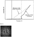
- FIG 4 represents the current circulating in the active layer of a conventional PCM memory, initially in its highly resistive state, as a function of the voltage applied to the terminals of its electrodes.
- the active material At the voltage shown in dotted lines called the threshold voltage, the active material is brought to its melting temperature.
- the melting of the active material in its amorphous state is necessary in order to subsequently carry out recrystallization making it possible to end up in the weakly resistive crystalline state.
- the active material in a liquid state is more conductive, which explains why the intensity increases significantly as a function of the voltage.
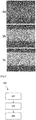
- FIG 1A shows three images obtained by transmission electron microscopy representing respectively the concentration of germanium Ge, antimony Sb and tellurium Te of the active layer of a conventional PCM memory produced in such an active material, after a programming cycle.
- a half-ring is visible corresponding to an enriched or impoverished zone.
- the concentration of antimony Sb is lower than the concentration in the rest of the active layer, while the tellurium concentration Te is greater than the concentration in the rest of the active layer.
- the invention offers a solution to the problems mentioned above, by providing a stable PCM memory with low programming time and high endurance.
- the proposed PCM memory is not subject to the phenomenon of segregation: it is therefore stable and meets the requirements in terms of endurance.
- the material of its active layer is not in an amorphous state but in a polycrystalline state comprising crystal cores. Therefore, to go from one resistive state to another and thus program the PCM memory, it suffices to increase / decrease the crystals by applying a given voltage lower than the threshold voltage which is necessary to pass from one state. amorphous to a crystalline state in conventional PCM memory. This therefore makes it possible to reduce the programming time, the electrical stress and the thermal stress, because there is no transition between a completely amorphous state and a crystalline state, as well as the mechanical stress, because there is less change. density and volume, and to avoid drift over time from the highly resistive state to greater resistive states.
- the memory according to a first aspect of the invention may have one or more additional characteristics among the following, considered individually or according to all the technically possible combinations.
- the ternary contains between 7 and 13% of germanium Ge and between 27 and 33% of tellurium Te.
- the ternary comprises 10% of germanium Ge, 27% of tellurium Te and 63% of Sb antimony.
- the active layer is doped.
- the cathode sputtering step uses a single sputtering target composed of the active material.
- the cathodic sputtering step uses three sputtering targets: a target composed of germanium Ge, a target composed of tellurium Te and a target composed of Sb antimony.
- the cathode sputtering step uses two sputtering targets: a target composed of the element of chemical formula Ge 2 Sb 2 Te 5 and a target composed of Sb antimony.
- the target composed of the element of chemical formula Ge 2 Sb 2 Te 5 being stable makes it possible to avoid the formation of aggregates.
- this target since this target is available on catalog, its cost is lower.
- a first aspect of the invention relates to a resistive phase change memory or PCM memory for “Phase-Change Memory”.
- FIG. 3C shows a schematic representation of the PCM memory 100 according to a first aspect of the invention.
- An upper electrode of a device is defined as the electrode located above this device and the lower electrode of a device as the electrode located below this device, the electrodes being located on either side. of the device.
- the adjectives “upper” and “lower” here relate to the orientation of the assembly including the upper electrode, the device and the lower electrode so that by turning this assembly over, the previously qualified electrode of upper becomes the lower electrode and the previously qualified lower electrode becomes the upper electrode.
- the lower 101 and upper 103 electrodes are each made from a conductive material which may be different or the same for the two electrodes 101, 103.
- a conductive material is, for example, TiN, TaN, W, TiWN, TiSiN or else WN.
- the active layer 102 is a layer of active material made from a ternary compound composed of germanium Ge, tellurium Te and antimony Sb.
- the percentage of Sb antimony contained in the active material is between 60 and 66%, that is to say that the active material is composed of 60 to 66% Sb antimony and 34 to 40% of germanium Ge and tellurium Te.
- germanium Ge and tellurium Te are divided into 7 to 13% germanium Ge and 27 to 33% tellurium Te.
- the active material is composed of 10% of germanium Ge, of 27% of tellurium Te and of 63% of Sb antimony.
- the active layer 102 is doped.
- the active layer 102 is for example doped with carbon C or nitrogen N.
- FIG 1B shows three images obtained by transmission electron microscopy representing respectively the concentration of germanium Ge, antimony Sb and tellurium Te of the active layer of the PCM memory 100 after a programming cycle. The greater the intensity at a point in the image, the greater the concentration of the component at that point.
- the composition of the active layer 102 of the PCM memory 100 is characterized by a polycrystalline phase and not by an amorphous phase in the highly resistive state, and by a single crystal phase in the weakly resistive state. More particularly, in the highly resistive state, the active layer 102 has crystal nuclei visible on the figure 5 .
- Fig 5 is an image obtained by nano-diffraction analysis on the material of the active layer of the PCM memory 100 showing crystal nuclei represented by bright white dots on the image.
- the passage from the weakly resistive state to the strongly resistive state is not characterized by a change of state, density and volume requiring the application of a threshold voltage but by a growth / decrease of crystals requiring the application of a voltage lower than the threshold voltage.
- the figure 4 represents the intensity circulating in the active layer of the PCM memory 100 as a function of the voltage applied to the terminals of its electrodes in addition to the intensity circulating in the active layer of a conventional PCM memory as described with reference to state of the art.
- the intensity increases linearly with the voltage at the terminals of the electrodes as soon as a voltage represented by a solid line, lower than the threshold voltage represented by dotted lines, has been passed.
- composition of the active layer 102 of the PCM memory 100 therefore makes it possible to reduce the electrical stress and the thermal stress due to the passage from a completely amorphous state to a crystalline state and to reduce the mechanical stress since there is less modification. density and volume and the fact of having crystal nuclei rather than an amorphous phase in the highly resistive state makes it possible to avoid drifting towards larger resistive states over time.
- a second aspect of the invention relates to a method of manufacturing resistive memory 100.
- FIG 2 shows a block diagram of steps 201 to 203 of the method 200 for manufacturing resistive memory 100.
- FIG 3A illustrates a first step 201 of the method 200 for manufacturing resistive memory 100.
- the first step 201 consists in carrying out a conformal deposition of a layer of conductive material of the lower electrode 101 on a substrate not shown on the figure. figure 3A .
- conformal deposition of a layer of material on a substrate means that the material is deposited uniformly over the entire surface of the substrate.
- the substrate can consist of one or more layers: it includes, for example, a layer with exposed copper lines allowing metallic contacts to be made with an upper metallic layer and thus includes all the logic necessary to allow the connection with the lines of the upper layers.
- FIG. 3B illustrates a second step 202 of the method 200 for manufacturing resistive memory 100.
- the second step 202 consists in using the cathode sputtering technique to form the active layer 102 of the resistive memory 100.
- cathodic sputtering uses the energy of a plasma at the surface of one or more sputtering targets, to tear off one by one the atoms of the material of the target (s) and deposit them. on a substrate.
- step 202 of cathodic sputtering uses a single sputtering target composed of a material having the same composition as the active material of the PCM memory 100 that it is desired to manufacture.
- the cathode sputtering step 202 then consists in sputtering the single target.
- the cathode sputtering step 202 uses three sputtering targets: a target composed of germanium Ge, a target composed of tellurium Te and a target composed of Sb antimony.
- the cathode sputtering step 202 then consists in co-sputtering the three targets so as to obtain the desired percentages for each component of the ternary.
- the cathode sputtering step 202 uses two sputtering targets: a target composed of the element of chemical formula Ge 2 Sb 2 Te 5 and a target composed of Sb antimony.
- the cathodic sputtering step 202 then consists of co-sputtering the two targets to obtain the desired percentages for each component of the ternary.
- sputtering targets produced in other materials, the preceding examples not being limiting.
- two sputtering targets can be used: a target composed of the element of chemical formula Ge 2 Te 5 and a target composed of Sb antimony.
- the spraying or co-spraying is for example carried out directly on the layer of conductive material of the lower electrode 101, as shown in the figure. figure 3B .
- the figure 3C illustrates a third step 203 of the method 200 for manufacturing resistive memory 100.
- the third step 203 consists in carrying out a conformal deposition of a layer of conductive material of the upper electrode 103.
- the conformal deposition is for example carried out directly on the active layer 102, as shown on the figure 3C .
- the manufacturing process 200 illustrated on figures 3A, 3B and 3C makes it possible to manufacture a PCM memory 100 of planar form but the PCM memory 100 could have a different form.
- the layer of conductive material of the lower electrode 101 comprises two branches arranged so as to have an “L” shape, the active layer 102 being in contact with the end of the branch of greater length.
- the manufacturing process of such a PCM memory 100 is then different from the manufacturing process 200.
- the manufacturing process 200 illustrated on figures 3A, 3B and 3C makes it possible to manufacture only the PCM memory 100, but the latter could also be manufactured to be co-integrated, for example with a selector device.
Landscapes
- Engineering & Computer Science (AREA)
- Manufacturing & Machinery (AREA)
- Semiconductor Memories (AREA)
Abstract
Description
- Le domaine technique de l'invention est celui des mémoires résistives à changement de phase.
- La présente invention concerne une mémoire résistive à changement de phase et en particulier une mémoire résistive à changement de phase dont le matériau actif est un ternaire composé de germanium Ge, de tellure Te et d'antimoine Sb. La présente invention concerne également un procédé de fabrication permettant d'obtenir une telle mémoire résistive.
- Grâce à leur capacité à augmenter les performances des ordinateurs tout en réduisant leur consommation, les mémoires de type SCM (pour « Storage Class Memory » ou mémoire à classe de stockage) caractérisées par un temps de programmation faible, inférieur à 10 ns et une grande endurance, de plus de 109 cycles, connaissent un essor important.
- Dans ce contexte, les mémoires résistives représentent de très bons candidats pour supporter le développement des mémoires SCM et parmi elles, les mémoires à changement de phase PCM (pour « Phase-Change Memory ») semblent être la technologie de mémoire résistive la plus mûre.
- Les mémoires résistives présentent au moins deux états correspondant au passage d'un état fortement résistif à un état faiblement résistif (SET) ou réciproquement (RESET).
- Les mémoires PCM classiques comportent deux électrodes et une couche active basée sur un matériau chalcogénure. Le fonctionnement des mémoires PCM classiques est basé sur la transition de phase du matériau chalcogénure, induite par l'échauffement de ce matériau sous l'effet d'impulsions électriques spécifiques générées par ses deux électrodes. Cette transition se fait entre une phase cristalline, ordonnée, de faible résistance et thermodynamiquement stable et une phase amorphe, désordonnée, de résistance élevée et thermodynamiquement instable.
- Le fonctionnement d'une mémoire PCM classique est illustré sur la
figure 4 . - [
Fig 4 ] représente l'intensité circulant dans la couche active d'une mémoire PCM classique, initialement dans son état fortement résistif, en fonction de la tension appliquée aux bornes de ses électrodes. - On constate que, pour des tensions inférieures à une tension représentée en pointillés, l'intensité circulant dans la couche active de la mémoire PCM classique varie peu à mesure que la tension aux bornes des électrodes augmente. En effet, la mémoire PCM étant dans son état amorphe, elle est faiblement conductrice.
- A la tension représentée en pointillés appelée tension seuil, le matériau actif est porté à sa température de fusion. La fusion du matériau actif dans son état amorphe est nécessaire pour réaliser par la suite une recristallisation permettant d'aboutir à l'état cristallin faiblement résistif. Un changement d'état entre un état solide peu conducteur et un état très conducteur, appelé claquage ou « switching », a donc lieu, ce qui se caractérise sur la courbe par des changements brutaux de variations au niveau de la tension seuil.
- Au-delà de cette tension seuil, le matériau actif dans un état liquide est plus conducteur, ce qui explique que l'intensité augmente de manière importante en fonction de la tension.
- Pour atteindre les performances en termes de temps de programmation et d'endurance demandées pour les mémoires SCM, différents matériaux actifs ont été proposés dans la littérature et notamment du Ge2Sb2Te5 enrichi en antimoine Sb d'un pourcentage compris entre 10 et 40%, l'ajout d'antimoine Sb ayant pour effet d'augmenter la vitesse de cristallisation.
- Cependant, de tels matériaux actifs sont sujets à un phénomène de ségrégation entraînant une perte de stabilité du matériau actif sous l'effet de la cristallisation.
- Ce phénomène de ségrégation est illustré sur la
figure 1A . - [
Fig 1A ] montre trois images obtenues par microscopie électronique en transmission représentant respectivement la concentration en germanium Ge, en antimoine Sb et en tellure Te de la couche active d'une mémoire PCM classique réalisée dans un tel matériau actif, après un cycle de programmation. Plus l'intensité en un point de l'image est importante, plus la concentration du composant en ce point est importante. - Pour chaque composant sur la
figure 1A est visible un demi-anneau correspondant à une zone enrichie ou appauvrie. Par exemple, on constate que, dans cette zone, la concentration d'antimoine Sb est inférieure à la concentration dans le reste de la couche active alors que la concentration en tellure Te est supérieure à la concentration dans le reste de la couche active. - Ce phénomène s'explique par la recherche de stabilité des composants, qui, soumis à une impulsion électrique, voient leur température et donc leur énergie augmenter, leur permettant de migrer pour établir des liaisons chimiques leur assurant un état énergétiquement plus stable. Ainsi, au fur et à mesure des cycles de programmation, le phénomène de ségrégation s'intensifie pour entraîner une perte de stabilité du matériau actif.
- Il existe donc un besoin de développer une mémoire PCM stable sous l'effet d'une impulsion électrique et susceptible de répondre aux spécifications des mémoires SCM.
- L'invention offre une solution aux problèmes évoqués précédemment, en proposant une mémoire PCM stable avec un temps de programmation faible et une grande endurance.
- Un premier aspect de l'invention concerne une mémoire résistive à changement de phase comportant :
- une électrode supérieure ;
- une électrode inférieure ;
- une couche réalisée dans un matériau actif, dite couche active ;
- Grâce à l'invention, la mémoire PCM proposée n'est pas soumise au phénomène de ségrégation : elle est donc stable et répond aux exigences en termes d'endurance. De plus, dans l'état fortement résistif, le matériau de sa couche active n'est pas dans un état amorphe mais dans un état polycristallin comportant des noyaux cristallins. De ce fait, pour passer d'un état résistif à l'autre et ainsi programmer la mémoire PCM, il suffit de faire croître/décroître les cristaux en appliquant une tension donnée inférieure à la tension seuil qui est nécessaire pour passer d'un état amorphe à un état cristallin dans une mémoire PCM classique. Ceci permet donc de diminuer le temps de programmation, le stress électrique et le stress thermique, car il n'y a pas de passage entre un état complètement amorphe et un état cristallin, ainsi que le stress mécanique, car il y a moins de changement de densité et de volume, et d'éviter la dérive au cours du temps de l'état fortement résistif vers des états résistifs plus importants.
- Outre les caractéristiques qui viennent d'être évoquées dans le paragraphe précédent, la mémoire selon un premier aspect de l'invention peut présenter une ou plusieurs caractéristiques complémentaires parmi les suivantes, considérées individuellement ou selon toutes les combinaisons techniquement possibles.
- Selon un exemple de réalisation, le ternaire comporte entre 7 et 13% de germanium Ge et entre 27 et 33% de tellure Te.
- Selon un exemple de réalisation compatible avec l'exemple de réalisation précédent, le ternaire comporte 10% de germanium Ge, 27% de tellure Te et 63% d'antimoine Sb.
- Selon un mode de réalisation compatible avec les exemples de réalisation précédent, la couche active est dopée.
- Un deuxième aspect de l'invention concerne un procédé de fabrication de la mémoire selon un premier aspect de l'invention comportant les étapes réalisées dans l'ordre suivant :
- une étape de dépôt conforme d'une couche de matériau conducteur d'électrode inférieure sur un substrat ;
- une étape de pulvérisation cathodique utilisant au moins une cible de pulvérisation pour former la couche active ;
- une étape de dépôt conforme d'une couche de matériau conducteur d'électrode supérieure.
- Selon un premier mode de réalisation, l'étape de pulvérisation cathodique utilise une unique cible de pulvérisation composée du matériau actif.
- Selon un deuxième mode de réalisation non compatible avec le premier mode de réalisation, l'étape de pulvérisation cathodique utilise trois cibles de pulvérisation : une cible composée de germanium Ge, une cible composée de tellure Te et une cible composée d'antimoine Sb.
- Selon un troisième mode de réalisation, l'étape de pulvérisation cathodique utilise deux cibles de pulvérisation : une cible composée de l'élément de formule chimique Ge2Sb2Te5 et une cible composée d'antimoine Sb.
- La cible composée de l'élément de formule chimique Ge2Sb2Te5 étant stable, son utilisation permet d'éviter la formation d'agrégats. De plus, cette cible étant disponible sur catalogue, son coût est moindre.
- L'invention et ses différentes applications seront mieux comprises à la lecture de la description qui suit et à l'examen des figures qui l'accompagnent.
- Les figures sont présentées à titre indicatif et nullement limitatif de l'invention.
- La
figure 1A montre trois images obtenues par microscopie électronique en transmission représentant respectivement la concentration en germanium Ge, en antimoine Sb et en tellure Te de la couche active d'une mémoire PCM ayant une composition selon l'art antérieur, après un cycle de programmation. - La
figure 1B montre trois images obtenues par microscopie électronique en transmission représentant respectivement la concentration en germanium Ge, en antimoine Sb et en tellure Te de la couche active d'une mémoire PCM selon un premier aspect de l'invention, après un cycle de programmation. - La
figure 2 montre le schéma synoptique d'un procédé de fabrication selon un deuxième aspect de l'invention. - La
figure 3A montre la représentation schématique d'une première étape du procédé selon un deuxième aspect de l'invention. - La
figure 3B montre la représentation schématique d'une deuxième étape du procédé selon un deuxième aspect de l'invention. - La
figure 3C montre la représentation schématique d'une troisième étape du procédé selon un deuxième aspect de l'invention. - La
figure 4 représente l'intensité circulant dans la couche active d'une mémoire selon un premier aspect de l'invention et dans la couche active d'une mémoire PCM classique, en fonction de la tension appliquée aux bornes de leurs électrodes, les mémoires se trouvant initialement dans leur état fortement résistif. - La
figure 5 montre une image obtenue par analyse de nano-diffraction ou « nano beam diffraction » sur le matériau de la couche active d'une mémoire selon un premier aspect de l'invention. - Sauf précision contraire, un même élément apparaissant sur des figures différentes présente une référence unique.
- La
figure 1A a déjà été décrite en référence à l'état de la technique. - Un premier aspect de l'invention concerne une mémoire résistive à changement de phase ou mémoire PCM pour « Phase-Change Memory ».
- [
Fig 3C ] montre une représentation schématique de la mémoire PCM 100 selon un premier aspect de l'invention. - La mémoire PCM 100 comporte :
- une électrode inférieure 101 ;
- une couche active 102 ; et
- une électrode supérieure 103.
- On définit une électrode supérieure d'un dispositif comme l'électrode située au-dessus de ce dispositif et l'électrode inférieure d'un dispositif comme l'électrode située en dessous de ce dispositif, les électrodes étant situées de part et d'autre du dispositif. Bien entendu, les adjectifs « supérieure » et « inférieure » sont ici relatifs à l'orientation de l'ensemble incluant l'électrode supérieure, le dispositif et l'électrode inférieure si bien qu'en retournant cet ensemble, l'électrode précédemment qualifiée de supérieure devient l'électrode inférieure et l'électrode précédemment qualifiée d'inférieure devient l'électrode supérieure.
- Les électrodes inférieure 101 et supérieure 103 sont réalisées chacune dans un matériau conducteur qui peut être différent ou le même pour les deux électrodes 101,103. Un tel matériau conducteur est par exemple du TiN, TaN, W, TiWN, TiSiN ou encore du WN.
- La couche active 102 est une couche de matériau actif réalisée en un ternaire composé de germanium Ge, de tellure Te et d'antimoine Sb. Le pourcentage d'antimoine Sb contenu dans le matériau actif est compris entre 60 et 66%, c'est-à-dire que le matériau actif est composé de 60 à 66% d'antimoine Sb et de 34 à 40% de germanium Ge et de tellure Te.
- Par exemple, les 34 à 40% de germanium Ge et de tellure Te se répartissent en 7 à 13% de germanium Ge et 27 à 33% de tellure Te.
- Selon un exemple de réalisation préféré, le matériau actif est composé de 10% de germanium Ge, de 27% de tellure Te et de 63% d'antimoine Sb.
- Selon un mode de réalisation, la couche active 102 est dopée. La couche active 102 est par exemple dopée avec du carbone C ou de l'azote N.
- [
Fig 1B ] montre trois images obtenues par microscopie électronique en transmission représentant respectivement la concentration en germanium Ge, en antimoine Sb et en tellure Te de la couche active de la mémoire PCM 100 après un cycle de programmation. Plus l'intensité en un point de l'image est importante, plus la concentration du composant en ce point est importante. - On constate l'absence du demi-anneau pour les trois composants et donc l'absence du phénomène de ségrégation.
- Ceci est très surprenant compte tenu du fait que dans l'état de la technique, le phénomène de ségrégation s'intensifie à mesure que l'on ajoute de l'antimoine Sb dans la composition du matériau actif.
- En plus de l'absence du phénomène de ségrégation, la composition de la couche active 102 de la mémoire PCM 100 se caractérise par une phase polycristalline et non pas par une phase amorphe dans l'état fortement résistif, et par une phase monocristalline dans l'état faiblement résistif. Plus particulièrement, dans l'état fortement résistif, la couche active 102 présente des noyaux cristallins visible sur la
figure 5 . - [
Fig 5 ] est une image obtenue par analyse de nano-diffraction sur le matériau de la couche active de la mémoire PCM 100 montrant des noyaux cristallins représentés par des points blancs lumineux sur l'image. - Ainsi, le passage de l'état faiblement résistif à l'état fortement résistif ne se caractérise pas par un changement d'état, de densité et de volume nécessitant l'application d'une tension seuil mais par une croissance/décroissance de cristaux nécessitant l'application d'une tension inférieure à la tension seuil.
- La
figure 4 représente l'intensité circulant dans la couche active de la mémoire PCM 100 en fonction de la tension appliquée aux bornes de ses électrodes en plus de l'intensité circulant dans la couche active d'une mémoire PCM classique telle que décrit en référence à l'état de la technique. - On constate que l'intensité augmente linéairement avec la tension aux bornes des électrodes dès qu'on a passé une tension représentée par un trait plein, inférieure à la tension de seuil représenté en pointillés.
- La composition de la couche active 102 de la mémoire PCM 100 permet donc de diminuer le stress électrique et le stress thermique dû au passage d'un état complètement amorphe à un état cristallin et de diminuer le stress mécanique puisqu'il y a moins de modification de densité et de volume et le fait d'avoir des noyaux cristallins plutôt qu'une phase amorphe dans l'état fortement résistif permet d'éviter la dérive vers des états résistifs plus importants au cours du temps.
- Un deuxième aspect de l'invention concerne un procédé de fabrication de la mémoire résistive 100.
- [
Fig 2 ] montre un schéma synoptique des étapes 201 à 203 du procédé 200 de fabrication de la mémoire résistive 100. - [
Fig 3A ] illustre une première étape 201 du procédé 200 de fabrication de la mémoire résistive 100. - La première étape 201 consiste à réaliser un dépôt conforme d'une couche de matériau conducteur d'électrode inférieure 101 sur un substrat non représenté sur la
figure 3A . - On entend par « dépôt conforme d'une couche de matériau sur un substrat » que le matériau est déposé de manière uniforme sur l'ensemble de la surface du substrat.
- Le substrat peut être constitué d'une ou de plusieurs couches : il comprend, par exemple, une couche avec des lignes en cuivre exposées permettant d'établir des contacts métalliques avec une couche métallique supérieure et comprend ainsi toute la logique nécessaire pour permettre la connexion avec les lignes des couches supérieures.
- [
Fig 3B ] illustre une deuxième étape 202 du procédé 200 de fabrication de la mémoire résistive 100. - La deuxième étape 202 consiste à utiliser la technique de pulvérisation cathodique pour former la couche active 102 de la mémoire résistive 100.
- Le principe de la pulvérisation cathodique est d'utiliser l'énergie d'un plasma à la surface d'une ou de plusieurs cibles de pulvérisation, pour arracher un à un les atomes du matériau de la ou des cible(s) et les déposer sur un substrat.
- Selon un premier mode de réalisation, l'étape 202 de pulvérisation cathodique utilise une unique cible de pulvérisation composée d'un matériau ayant la même composition que le matériau actif de la mémoire PCM 100 que l'on souhaite fabriquer. L'étape 202 de pulvérisation cathodique consiste alors à pulvériser l'unique cible.
- Selon un deuxième mode de réalisation, l'étape 202 de pulvérisation cathodique utilise trois cibles de pulvérisation : une cible composée de germanium Ge, une cible composée de tellure Te et une cible composée d'antimoine Sb. L'étape 202 de pulvérisation cathodique consiste alors à co-pulvériser les trois cibles de manière à obtenir les pourcentages souhaités pour chaque composant du ternaire.
- Selon un troisième mode de réalisation, l'étape 202 de pulvérisation cathodique utilise deux cibles de pulvérisation : une cible composée de l'élément de formule chimique Ge2Sb2Te5 et une cible composée d'antimoine Sb. L'étape 202 de pulvérisation cathodique consiste alors à co-pulvériser les deux cibles pour obtenir les pourcentages souhaités pour chaque composant du ternaire.
- Il est également possible d'utiliser d'autres cibles de pulvérisation réalisées dans d'autres matériaux, les exemples précédents n'étant pas limitatifs. On peut, par exemple, utiliser trois cibles de pulvérisation : une cible composée de l'élément de formule chimique GeTe, une cible composée de l'élément de formule chimique Sb2Te3 et une cible composée d'antimoine Sb. On peut par exemple utiliser deux cibles de pulvérisation : une cible composée de l'élément de formule chimique Ge2Te5 et une cible composée d'antimoine Sb.
- La pulvérisation ou la co-pulvérisation est par exemple réalisée directement sur la couche de matériau conducteur d'électrode inférieure 101, comme représentée sur la
figure 3B . - La
figure 3C illustre une troisième étape 203 du procédé 200 de fabrication de la mémoire résistive 100. - La troisième étape 203 consiste à réaliser un dépôt conforme d'une couche de matériau conducteur d'électrode supérieure 103.
- Le dépôt conforme est par exemple réalisé directement sur la couche active 102, comme représentée sur la
figure 3C . - Le procédé 200 de fabrication illustré sur les
figures 3A, 3B et 3C permet de fabriquer une mémoire PCM 100 de forme planaire mais la mémoire PCM 100 pourrait présenter une forme différente. Par exemple, la couche de matériau conducteur d'électrode inférieure 101 comporte deux branches agencées de manière à présenter une forme en « L », la couche active 102 étant en contact avec l'extrémité de la branche de plus grande longueur. Le procédé de fabrication d'une telle mémoire PCM 100 est alors différent du procédé de fabrication 200. - Le procédé 200 de fabrication illustré sur les
figures 3A, 3B et 3C permet de fabriquer uniquement la mémoire PCM 100 mais celle-ci pourrait également être fabriquée pour être co-intégrée, par exemple avec un dispositif sélecteur.
Claims (4)
- Procédé (200) de fabrication d'une mémoire (100) résistive à changement de phase comportant :- une électrode supérieure (103) ;- une électrode inférieure (101) ;- une couche réalisée dans un matériau actif, dite couche active (102) ;la mémoire (100) passant d'un état fortement résistif à un état faiblement résistif par application d'une tension entre l'électrode supérieure (103) et l'électrode inférieure (101), le matériau de la couche active (102) étant un ternaire composé de germanium Ge, de tellure Te et d'antimoine Sb, le ternaire comportant entre 60 et 66% d'antimoine Sb, le procédé comportant les étapes réalisées dans l'ordre suivant :- une étape (201) de dépôt conforme d'une couche de matériau conducteur d'électrode inférieure (101) sur un substrat ;- une étape (202) de pulvérisation cathodique utilisant deux cibles de pulvérisation pour former la couche active (102), une cible composée de l'élément de formule chimique Ge2Sb2Te5 et une cible composée d'antimoine Sb ;- une étape (203) de dépôt conforme d'une couche de matériau conducteur d'électrode supérieure (103).
- Procédé (200) selon la revendication 1, caractérisée en ce que le ternaire comporte entre 7 et 13% de germanium Ge et entre 27 et 33% de tellure Te.
- Procédé (200) selon l'une quelconque des revendications 1 à 2, caractérisée en ce que le ternaire comporte 10% de germanium Ge, 27% de tellure Te et 63% d'antimoine Sb.
- Procédé (200) selon l'une quelconque des revendications précédentes, caractérisée en ce que la couche active (102) est dopée.
Applications Claiming Priority (1)
| Application Number | Priority Date | Filing Date | Title |
|---|---|---|---|
| FR1900749A FR3092200B1 (fr) | 2019-01-28 | 2019-01-28 | Memoire resistive a changement de phase |
Publications (2)
| Publication Number | Publication Date |
|---|---|
| EP3686942A1 true EP3686942A1 (fr) | 2020-07-29 |
| EP3686942B1 EP3686942B1 (fr) | 2021-11-10 |
Family
ID=67107685
Family Applications (1)
| Application Number | Title | Priority Date | Filing Date |
|---|---|---|---|
| EP20153899.8A Active EP3686942B1 (fr) | 2019-01-28 | 2020-01-27 | Procédé de fabrication d'une memoire resistive a changement de phase |
Country Status (3)
| Country | Link |
|---|---|
| US (1) | US11707001B2 (fr) |
| EP (1) | EP3686942B1 (fr) |
| FR (1) | FR3092200B1 (fr) |
Citations (2)
| Publication number | Priority date | Publication date | Assignee | Title |
|---|---|---|---|---|
| US20070034849A1 (en) * | 2005-08-09 | 2007-02-15 | Ovonyx, Inc. | Multi-layer chalcogenide devices |
| US20090286037A1 (en) * | 2006-11-01 | 2009-11-19 | Matsushita Electric Industrial Co., Ltd. | Information recording medium, target and method for manufacturing of information recording medium using the same |
Family Cites Families (7)
| Publication number | Priority date | Publication date | Assignee | Title |
|---|---|---|---|---|
| US7227170B2 (en) * | 2003-03-10 | 2007-06-05 | Energy Conversion Devices, Inc. | Multiple bit chalcogenide storage device |
| US7742330B2 (en) * | 2004-05-25 | 2010-06-22 | Renesas Technology Corp. | Semiconductor device |
| US7525117B2 (en) * | 2005-08-09 | 2009-04-28 | Ovonyx, Inc. | Chalcogenide devices and materials having reduced germanium or telluruim content |
| US7501648B2 (en) * | 2006-08-16 | 2009-03-10 | International Business Machines Corporation | Phase change materials and associated memory devices |
| JP4929228B2 (ja) * | 2008-01-23 | 2012-05-09 | 韓國電子通信研究院 | 相変化メモリー素子及びその製造方法 |
| KR100990215B1 (ko) * | 2008-07-17 | 2010-10-29 | 한국전자통신연구원 | 상변화 메모리 소자 및 그 제조 방법 |
| US9613689B1 (en) * | 2016-07-08 | 2017-04-04 | Sandisk Technologies Llc | Self-selecting local bit line for a three-dimensional memory array |
-
2019
- 2019-01-28 FR FR1900749A patent/FR3092200B1/fr not_active Expired - Fee Related
-
2020
- 2020-01-27 EP EP20153899.8A patent/EP3686942B1/fr active Active
- 2020-01-27 US US16/773,226 patent/US11707001B2/en active Active
Patent Citations (2)
| Publication number | Priority date | Publication date | Assignee | Title |
|---|---|---|---|---|
| US20070034849A1 (en) * | 2005-08-09 | 2007-02-15 | Ovonyx, Inc. | Multi-layer chalcogenide devices |
| US20090286037A1 (en) * | 2006-11-01 | 2009-11-19 | Matsushita Electric Industrial Co., Ltd. | Information recording medium, target and method for manufacturing of information recording medium using the same |
Non-Patent Citations (2)
| Title |
|---|
| CHEONG B-K ET AL: "Characteristics of Phase Change Memory Devices based on Ge-doped SbTe and its derivative", 2007, XP055642181, Retrieved from the Internet <URL:https://www.epcos.org/e-pcos-2007> [retrieved on 20191114] * |
| WU Z ET AL: "Controlled recrystallization for low-current RESET programming characteristics of phase-change memory with Ge-doped SbTe", APPLIED PHYSICS LETTERS, vol. 99, no. 14, 143505, 3 October 2011 (2011-10-03), XP012153225, ISSN: 0003-6951, DOI: 10.1063/1.3641470 * |
Also Published As
| Publication number | Publication date |
|---|---|
| EP3686942B1 (fr) | 2021-11-10 |
| US11707001B2 (en) | 2023-07-18 |
| FR3092200A1 (fr) | 2020-07-31 |
| FR3092200B1 (fr) | 2021-10-22 |
| US20200243766A1 (en) | 2020-07-30 |
Similar Documents
| Publication | Publication Date | Title |
|---|---|---|
| US9054295B2 (en) | Phase change memory cells including nitrogenated carbon materials, methods of forming the same, and phase change memory devices including nitrogenated carbon materials | |
| US7483293B2 (en) | Method for improving the thermal characteristics of semiconductor memory cells | |
| JP5636617B2 (ja) | カルコゲナイド勾配を有するカルコゲナイド含有半導体 | |
| US20080093589A1 (en) | Resistance variable devices with controllable channels | |
| EP3614446B1 (fr) | Elément de mémorisation | |
| FR2934711A1 (fr) | Dispositif memoire et memoire cbram a fiablilite amelioree. | |
| EP4078678A1 (fr) | Cellule elementaire comportant une memoire resistive et un dispositif destine a former un selecteur, matrice de cellules, procedes de fabrication et d'initialisation associes | |
| EP1683157A1 (fr) | Element de memoire a changement de phase a cyclabilite amelioree | |
| FR2880177A1 (fr) | Memoire pmc ayant un temps de retention et une vitesse d'ecriture ameliores | |
| EP3506377B1 (fr) | Cellule elementaire comportant une memoire resistive et un selecteur, etage et matrice d'etages comportant une pluralite de ces cellules et procede de fabrication associe | |
| EP3940803B1 (fr) | Matériau destiné à changer de phase et mémoire résistive à changement de phase associée | |
| EP3686942B1 (fr) | Procédé de fabrication d'une memoire resistive a changement de phase | |
| EP3863075B1 (fr) | Elément de sélection et procédé de fabrication correspondant | |
| EP2472624B1 (fr) | Procédé de gravure d'un dispositif microélectronique à mémoire programmable | |
| EP4339952A1 (fr) | Cellule mémoire à changement de phase | |
| EP4391786B1 (fr) | Un dispositif mémoire à changement de phase et un procédé de fabrication d'un dispositif mémoire à changement de phase | |
| EP4557932B1 (fr) | Cellule mémoire à changement de phase et procédé de fabrication correspondant | |
| EP4577030B1 (fr) | Dispositif mémoire à changement de phase à tenue en température améliorée et procédé | |
| KR100998887B1 (ko) | 상 변화 물질을 이용한 전자 소자, 상 변화 메모리 소자 및이의 제조 방법 | |
| EP4526881A1 (fr) | Mémoire résistive à performances configurables et procédés associés | |
| WO2020249697A1 (fr) | Procédé de détermination d'un paramètre de fabrication d'une cellule de mémoire vive résistive | |
| EP3984073A1 (fr) | Procédé de fabrication d'une cellule mémoire résistive de type oxram |
Legal Events
| Date | Code | Title | Description |
|---|---|---|---|
| PUAI | Public reference made under article 153(3) epc to a published international application that has entered the european phase |
Free format text: ORIGINAL CODE: 0009012 |
|
| STAA | Information on the status of an ep patent application or granted ep patent |
Free format text: STATUS: REQUEST FOR EXAMINATION WAS MADE |
|
| 17P | Request for examination filed |
Effective date: 20200127 |
|
| AK | Designated contracting states |
Kind code of ref document: A1 Designated state(s): AL AT BE BG CH CY CZ DE DK EE ES FI FR GB GR HR HU IE IS IT LI LT LU LV MC MK MT NL NO PL PT RO RS SE SI SK SM TR |
|
| AX | Request for extension of the european patent |
Extension state: BA ME |
|
| RBV | Designated contracting states (corrected) |
Designated state(s): AL AT BE BG CH CY CZ DE DK EE ES FI FR GB GR HR HU IE IS IT LI LT LU LV MC MK MT NL NO PL PT RO RS SE SI SK SM TR |
|
| GRAP | Despatch of communication of intention to grant a patent |
Free format text: ORIGINAL CODE: EPIDOSNIGR1 |
|
| STAA | Information on the status of an ep patent application or granted ep patent |
Free format text: STATUS: GRANT OF PATENT IS INTENDED |
|
| INTG | Intention to grant announced |
Effective date: 20210602 |
|
| GRAS | Grant fee paid |
Free format text: ORIGINAL CODE: EPIDOSNIGR3 |
|
| GRAA | (expected) grant |
Free format text: ORIGINAL CODE: 0009210 |
|
| STAA | Information on the status of an ep patent application or granted ep patent |
Free format text: STATUS: THE PATENT HAS BEEN GRANTED |
|
| AK | Designated contracting states |
Kind code of ref document: B1 Designated state(s): AL AT BE BG CH CY CZ DE DK EE ES FI FR GB GR HR HU IE IS IT LI LT LU LV MC MK MT NL NO PL PT RO RS SE SI SK SM TR |
|
| REG | Reference to a national code |
Ref country code: GB Ref legal event code: FG4D Free format text: NOT ENGLISH |
|
| REG | Reference to a national code |
Ref country code: AT Ref legal event code: REF Ref document number: 1446892 Country of ref document: AT Kind code of ref document: T Effective date: 20211115 Ref country code: CH Ref legal event code: EP |
|
| REG | Reference to a national code |
Ref country code: DE Ref legal event code: R096 Ref document number: 602020000931 Country of ref document: DE |
|
| REG | Reference to a national code |
Ref country code: IE Ref legal event code: FG4D Free format text: LANGUAGE OF EP DOCUMENT: FRENCH |
|
| REG | Reference to a national code |
Ref country code: LT Ref legal event code: MG9D |
|
| REG | Reference to a national code |
Ref country code: NL Ref legal event code: MP Effective date: 20211110 |
|
| REG | Reference to a national code |
Ref country code: AT Ref legal event code: MK05 Ref document number: 1446892 Country of ref document: AT Kind code of ref document: T Effective date: 20211110 |
|
| PG25 | Lapsed in a contracting state [announced via postgrant information from national office to epo] |
Ref country code: RS Free format text: LAPSE BECAUSE OF FAILURE TO SUBMIT A TRANSLATION OF THE DESCRIPTION OR TO PAY THE FEE WITHIN THE PRESCRIBED TIME-LIMIT Effective date: 20211110 Ref country code: LT Free format text: LAPSE BECAUSE OF FAILURE TO SUBMIT A TRANSLATION OF THE DESCRIPTION OR TO PAY THE FEE WITHIN THE PRESCRIBED TIME-LIMIT Effective date: 20211110 Ref country code: FI Free format text: LAPSE BECAUSE OF FAILURE TO SUBMIT A TRANSLATION OF THE DESCRIPTION OR TO PAY THE FEE WITHIN THE PRESCRIBED TIME-LIMIT Effective date: 20211110 Ref country code: BG Free format text: LAPSE BECAUSE OF FAILURE TO SUBMIT A TRANSLATION OF THE DESCRIPTION OR TO PAY THE FEE WITHIN THE PRESCRIBED TIME-LIMIT Effective date: 20220210 Ref country code: AT Free format text: LAPSE BECAUSE OF FAILURE TO SUBMIT A TRANSLATION OF THE DESCRIPTION OR TO PAY THE FEE WITHIN THE PRESCRIBED TIME-LIMIT Effective date: 20211110 |
|
| PG25 | Lapsed in a contracting state [announced via postgrant information from national office to epo] |
Ref country code: IS Free format text: LAPSE BECAUSE OF FAILURE TO SUBMIT A TRANSLATION OF THE DESCRIPTION OR TO PAY THE FEE WITHIN THE PRESCRIBED TIME-LIMIT Effective date: 20220310 Ref country code: SE Free format text: LAPSE BECAUSE OF FAILURE TO SUBMIT A TRANSLATION OF THE DESCRIPTION OR TO PAY THE FEE WITHIN THE PRESCRIBED TIME-LIMIT Effective date: 20211110 Ref country code: PT Free format text: LAPSE BECAUSE OF FAILURE TO SUBMIT A TRANSLATION OF THE DESCRIPTION OR TO PAY THE FEE WITHIN THE PRESCRIBED TIME-LIMIT Effective date: 20220310 Ref country code: PL Free format text: LAPSE BECAUSE OF FAILURE TO SUBMIT A TRANSLATION OF THE DESCRIPTION OR TO PAY THE FEE WITHIN THE PRESCRIBED TIME-LIMIT Effective date: 20211110 Ref country code: NO Free format text: LAPSE BECAUSE OF FAILURE TO SUBMIT A TRANSLATION OF THE DESCRIPTION OR TO PAY THE FEE WITHIN THE PRESCRIBED TIME-LIMIT Effective date: 20220210 Ref country code: NL Free format text: LAPSE BECAUSE OF FAILURE TO SUBMIT A TRANSLATION OF THE DESCRIPTION OR TO PAY THE FEE WITHIN THE PRESCRIBED TIME-LIMIT Effective date: 20211110 Ref country code: LV Free format text: LAPSE BECAUSE OF FAILURE TO SUBMIT A TRANSLATION OF THE DESCRIPTION OR TO PAY THE FEE WITHIN THE PRESCRIBED TIME-LIMIT Effective date: 20211110 Ref country code: HR Free format text: LAPSE BECAUSE OF FAILURE TO SUBMIT A TRANSLATION OF THE DESCRIPTION OR TO PAY THE FEE WITHIN THE PRESCRIBED TIME-LIMIT Effective date: 20211110 Ref country code: GR Free format text: LAPSE BECAUSE OF FAILURE TO SUBMIT A TRANSLATION OF THE DESCRIPTION OR TO PAY THE FEE WITHIN THE PRESCRIBED TIME-LIMIT Effective date: 20220211 Ref country code: ES Free format text: LAPSE BECAUSE OF FAILURE TO SUBMIT A TRANSLATION OF THE DESCRIPTION OR TO PAY THE FEE WITHIN THE PRESCRIBED TIME-LIMIT Effective date: 20211110 |
|
| PG25 | Lapsed in a contracting state [announced via postgrant information from national office to epo] |
Ref country code: SM Free format text: LAPSE BECAUSE OF FAILURE TO SUBMIT A TRANSLATION OF THE DESCRIPTION OR TO PAY THE FEE WITHIN THE PRESCRIBED TIME-LIMIT Effective date: 20211110 Ref country code: SK Free format text: LAPSE BECAUSE OF FAILURE TO SUBMIT A TRANSLATION OF THE DESCRIPTION OR TO PAY THE FEE WITHIN THE PRESCRIBED TIME-LIMIT Effective date: 20211110 Ref country code: RO Free format text: LAPSE BECAUSE OF FAILURE TO SUBMIT A TRANSLATION OF THE DESCRIPTION OR TO PAY THE FEE WITHIN THE PRESCRIBED TIME-LIMIT Effective date: 20211110 Ref country code: EE Free format text: LAPSE BECAUSE OF FAILURE TO SUBMIT A TRANSLATION OF THE DESCRIPTION OR TO PAY THE FEE WITHIN THE PRESCRIBED TIME-LIMIT Effective date: 20211110 Ref country code: DK Free format text: LAPSE BECAUSE OF FAILURE TO SUBMIT A TRANSLATION OF THE DESCRIPTION OR TO PAY THE FEE WITHIN THE PRESCRIBED TIME-LIMIT Effective date: 20211110 Ref country code: CZ Free format text: LAPSE BECAUSE OF FAILURE TO SUBMIT A TRANSLATION OF THE DESCRIPTION OR TO PAY THE FEE WITHIN THE PRESCRIBED TIME-LIMIT Effective date: 20211110 |
|
| REG | Reference to a national code |
Ref country code: DE Ref legal event code: R097 Ref document number: 602020000931 Country of ref document: DE |
|
| PG25 | Lapsed in a contracting state [announced via postgrant information from national office to epo] |
Ref country code: MC Free format text: LAPSE BECAUSE OF FAILURE TO SUBMIT A TRANSLATION OF THE DESCRIPTION OR TO PAY THE FEE WITHIN THE PRESCRIBED TIME-LIMIT Effective date: 20211110 |
|
| PLBE | No opposition filed within time limit |
Free format text: ORIGINAL CODE: 0009261 |
|
| STAA | Information on the status of an ep patent application or granted ep patent |
Free format text: STATUS: NO OPPOSITION FILED WITHIN TIME LIMIT |
|
| REG | Reference to a national code |
Ref country code: BE Ref legal event code: MM Effective date: 20220131 |
|
| 26N | No opposition filed |
Effective date: 20220811 |
|
| PG25 | Lapsed in a contracting state [announced via postgrant information from national office to epo] |
Ref country code: LU Free format text: LAPSE BECAUSE OF NON-PAYMENT OF DUE FEES Effective date: 20220127 Ref country code: AL Free format text: LAPSE BECAUSE OF FAILURE TO SUBMIT A TRANSLATION OF THE DESCRIPTION OR TO PAY THE FEE WITHIN THE PRESCRIBED TIME-LIMIT Effective date: 20211110 |
|
| REG | Reference to a national code |
Ref country code: DE Ref legal event code: R079 Ref document number: 602020000931 Country of ref document: DE Free format text: PREVIOUS MAIN CLASS: H01L0045000000 Ipc: H10N0070000000 |
|
| PG25 | Lapsed in a contracting state [announced via postgrant information from national office to epo] |
Ref country code: SI Free format text: LAPSE BECAUSE OF FAILURE TO SUBMIT A TRANSLATION OF THE DESCRIPTION OR TO PAY THE FEE WITHIN THE PRESCRIBED TIME-LIMIT Effective date: 20211110 Ref country code: BE Free format text: LAPSE BECAUSE OF NON-PAYMENT OF DUE FEES Effective date: 20220131 |
|
| PG25 | Lapsed in a contracting state [announced via postgrant information from national office to epo] |
Ref country code: IE Free format text: LAPSE BECAUSE OF NON-PAYMENT OF DUE FEES Effective date: 20220127 |
|
| PG25 | Lapsed in a contracting state [announced via postgrant information from national office to epo] |
Ref country code: IT Free format text: LAPSE BECAUSE OF FAILURE TO SUBMIT A TRANSLATION OF THE DESCRIPTION OR TO PAY THE FEE WITHIN THE PRESCRIBED TIME-LIMIT Effective date: 20211110 |
|
| REG | Reference to a national code |
Ref country code: CH Ref legal event code: PL |
|
| PG25 | Lapsed in a contracting state [announced via postgrant information from national office to epo] |
Ref country code: LI Free format text: LAPSE BECAUSE OF NON-PAYMENT OF DUE FEES Effective date: 20230131 Ref country code: CH Free format text: LAPSE BECAUSE OF NON-PAYMENT OF DUE FEES Effective date: 20230131 |
|
| PG25 | Lapsed in a contracting state [announced via postgrant information from national office to epo] |
Ref country code: MK Free format text: LAPSE BECAUSE OF FAILURE TO SUBMIT A TRANSLATION OF THE DESCRIPTION OR TO PAY THE FEE WITHIN THE PRESCRIBED TIME-LIMIT Effective date: 20211110 Ref country code: CY Free format text: LAPSE BECAUSE OF FAILURE TO SUBMIT A TRANSLATION OF THE DESCRIPTION OR TO PAY THE FEE WITHIN THE PRESCRIBED TIME-LIMIT Effective date: 20211110 |
|
| PG25 | Lapsed in a contracting state [announced via postgrant information from national office to epo] |
Ref country code: HU Free format text: LAPSE BECAUSE OF FAILURE TO SUBMIT A TRANSLATION OF THE DESCRIPTION OR TO PAY THE FEE WITHIN THE PRESCRIBED TIME-LIMIT; INVALID AB INITIO Effective date: 20200127 |
|
| PG25 | Lapsed in a contracting state [announced via postgrant information from national office to epo] |
Ref country code: TR Free format text: LAPSE BECAUSE OF FAILURE TO SUBMIT A TRANSLATION OF THE DESCRIPTION OR TO PAY THE FEE WITHIN THE PRESCRIBED TIME-LIMIT Effective date: 20211110 |
|
| PG25 | Lapsed in a contracting state [announced via postgrant information from national office to epo] |
Ref country code: MT Free format text: LAPSE BECAUSE OF FAILURE TO SUBMIT A TRANSLATION OF THE DESCRIPTION OR TO PAY THE FEE WITHIN THE PRESCRIBED TIME-LIMIT Effective date: 20211110 |
|
| PGFP | Annual fee paid to national office [announced via postgrant information from national office to epo] |
Ref country code: GB Payment date: 20260121 Year of fee payment: 7 |
|
| PGFP | Annual fee paid to national office [announced via postgrant information from national office to epo] |
Ref country code: DE Payment date: 20260120 Year of fee payment: 7 |
|
| PGFP | Annual fee paid to national office [announced via postgrant information from national office to epo] |
Ref country code: FR Payment date: 20260123 Year of fee payment: 7 |