EP3686923A1 - Semiconductor die with improved thermal insulation between a power portion and a peripheral portion, method of manufacturing, and package housing the die - Google Patents
Semiconductor die with improved thermal insulation between a power portion and a peripheral portion, method of manufacturing, and package housing the die Download PDFInfo
- Publication number
- EP3686923A1 EP3686923A1 EP20154200.8A EP20154200A EP3686923A1 EP 3686923 A1 EP3686923 A1 EP 3686923A1 EP 20154200 A EP20154200 A EP 20154200A EP 3686923 A1 EP3686923 A1 EP 3686923A1
- Authority
- EP
- European Patent Office
- Prior art keywords
- trench
- region
- structural body
- along
- insulation means
- Prior art date
- Legal status (The legal status is an assumption and is not a legal conclusion. Google has not performed a legal analysis and makes no representation as to the accuracy of the status listed.)
- Granted
Links
Images



Classifications
-
- H—ELECTRICITY
- H10—SEMICONDUCTOR DEVICES; ELECTRIC SOLID-STATE DEVICES NOT OTHERWISE PROVIDED FOR
- H10W—GENERIC PACKAGES, INTERCONNECTIONS, CONNECTORS OR OTHER CONSTRUCTIONAL DETAILS OF DEVICES COVERED BY CLASS H10
- H10W90/00—Package configurations
-
- F—MECHANICAL ENGINEERING; LIGHTING; HEATING; WEAPONS; BLASTING
- F16—ENGINEERING ELEMENTS AND UNITS; GENERAL MEASURES FOR PRODUCING AND MAINTAINING EFFECTIVE FUNCTIONING OF MACHINES OR INSTALLATIONS; THERMAL INSULATION IN GENERAL
- F16L—PIPES; JOINTS OR FITTINGS FOR PIPES; SUPPORTS FOR PIPES, CABLES OR PROTECTIVE TUBING; MEANS FOR THERMAL INSULATION IN GENERAL
- F16L59/00—Thermal insulation in general
- F16L59/02—Shape or form of insulating materials, with or without coverings integral with the insulating materials
-
- H—ELECTRICITY
- H10—SEMICONDUCTOR DEVICES; ELECTRIC SOLID-STATE DEVICES NOT OTHERWISE PROVIDED FOR
- H10D—INORGANIC ELECTRIC SEMICONDUCTOR DEVICES
- H10D84/00—Integrated devices formed in or on semiconductor substrates that comprise only semiconducting layers, e.g. on Si wafers or on GaAs-on-Si wafers
- H10D84/01—Manufacture or treatment
- H10D84/0123—Integrating together multiple components covered by H10D12/00 or H10D30/00, e.g. integrating multiple IGBTs
-
- H—ELECTRICITY
- H10—SEMICONDUCTOR DEVICES; ELECTRIC SOLID-STATE DEVICES NOT OTHERWISE PROVIDED FOR
- H10D—INORGANIC ELECTRIC SEMICONDUCTOR DEVICES
- H10D84/00—Integrated devices formed in or on semiconductor substrates that comprise only semiconducting layers, e.g. on Si wafers or on GaAs-on-Si wafers
- H10D84/01—Manufacture or treatment
- H10D84/02—Manufacture or treatment characterised by using material-based technologies
- H10D84/08—Manufacture or treatment characterised by using material-based technologies using combinations of technologies, e.g. using both Si and SiC technologies or using both Si and Group III-V technologies
-
- H—ELECTRICITY
- H10—SEMICONDUCTOR DEVICES; ELECTRIC SOLID-STATE DEVICES NOT OTHERWISE PROVIDED FOR
- H10D—INORGANIC ELECTRIC SEMICONDUCTOR DEVICES
- H10D89/00—Aspects of integrated devices not covered by groups H10D84/00 - H10D88/00
- H10D89/10—Integrated device layouts
- H10D89/105—Integrated device layouts adapted for thermal considerations
-
- H—ELECTRICITY
- H10—SEMICONDUCTOR DEVICES; ELECTRIC SOLID-STATE DEVICES NOT OTHERWISE PROVIDED FOR
- H10W—GENERIC PACKAGES, INTERCONNECTIONS, CONNECTORS OR OTHER CONSTRUCTIONAL DETAILS OF DEVICES COVERED BY CLASS H10
- H10W10/00—Isolation regions in semiconductor bodies between components of integrated devices
- H10W10/01—Manufacture or treatment
- H10W10/011—Manufacture or treatment of isolation regions comprising dielectric materials
- H10W10/014—Manufacture or treatment of isolation regions comprising dielectric materials using trench refilling with dielectric materials, e.g. shallow trench isolations
-
- H—ELECTRICITY
- H10—SEMICONDUCTOR DEVICES; ELECTRIC SOLID-STATE DEVICES NOT OTHERWISE PROVIDED FOR
- H10W—GENERIC PACKAGES, INTERCONNECTIONS, CONNECTORS OR OTHER CONSTRUCTIONAL DETAILS OF DEVICES COVERED BY CLASS H10
- H10W10/00—Isolation regions in semiconductor bodies between components of integrated devices
- H10W10/01—Manufacture or treatment
- H10W10/041—Manufacture or treatment of isolation regions comprising polycrystalline semiconductor materials
-
- H—ELECTRICITY
- H10—SEMICONDUCTOR DEVICES; ELECTRIC SOLID-STATE DEVICES NOT OTHERWISE PROVIDED FOR
- H10W—GENERIC PACKAGES, INTERCONNECTIONS, CONNECTORS OR OTHER CONSTRUCTIONAL DETAILS OF DEVICES COVERED BY CLASS H10
- H10W10/00—Isolation regions in semiconductor bodies between components of integrated devices
- H10W10/10—Isolation regions comprising dielectric materials
- H10W10/17—Isolation regions comprising dielectric materials formed using trench refilling with dielectric materials, e.g. shallow trench isolations
-
- H—ELECTRICITY
- H10—SEMICONDUCTOR DEVICES; ELECTRIC SOLID-STATE DEVICES NOT OTHERWISE PROVIDED FOR
- H10W—GENERIC PACKAGES, INTERCONNECTIONS, CONNECTORS OR OTHER CONSTRUCTIONAL DETAILS OF DEVICES COVERED BY CLASS H10
- H10W10/00—Isolation regions in semiconductor bodies between components of integrated devices
- H10W10/40—Isolation regions comprising polycrystalline semiconductor materials
-
- H—ELECTRICITY
- H10—SEMICONDUCTOR DEVICES; ELECTRIC SOLID-STATE DEVICES NOT OTHERWISE PROVIDED FOR
- H10W—GENERIC PACKAGES, INTERCONNECTIONS, CONNECTORS OR OTHER CONSTRUCTIONAL DETAILS OF DEVICES COVERED BY CLASS H10
- H10W40/00—Arrangements for thermal protection or thermal control
- H10W40/20—Arrangements for cooling
- H10W40/22—Arrangements for cooling characterised by their shape, e.g. having conical or cylindrical projections
-
- H—ELECTRICITY
- H10—SEMICONDUCTOR DEVICES; ELECTRIC SOLID-STATE DEVICES NOT OTHERWISE PROVIDED FOR
- H10W—GENERIC PACKAGES, INTERCONNECTIONS, CONNECTORS OR OTHER CONSTRUCTIONAL DETAILS OF DEVICES COVERED BY CLASS H10
- H10W42/00—Arrangements for protection of devices
-
- H—ELECTRICITY
- H10—SEMICONDUCTOR DEVICES; ELECTRIC SOLID-STATE DEVICES NOT OTHERWISE PROVIDED FOR
- H10D—INORGANIC ELECTRIC SEMICONDUCTOR DEVICES
- H10D30/00—Field-effect transistors [FET]
- H10D30/40—FETs having zero-dimensional [0D], one-dimensional [1D] or two-dimensional [2D] charge carrier gas channels
- H10D30/47—FETs having zero-dimensional [0D], one-dimensional [1D] or two-dimensional [2D] charge carrier gas channels having two-dimensional [2D] charge carrier gas channels, e.g. nanoribbon FETs or high electron mobility transistors [HEMT]
- H10D30/471—High electron mobility transistors [HEMT] or high hole mobility transistors [HHMT]
- H10D30/475—High electron mobility transistors [HEMT] or high hole mobility transistors [HHMT] having wider bandgap layer formed on top of lower bandgap active layer, e.g. undoped barrier HEMTs such as i-AlGaN/GaN HEMTs
-
- H—ELECTRICITY
- H10—SEMICONDUCTOR DEVICES; ELECTRIC SOLID-STATE DEVICES NOT OTHERWISE PROVIDED FOR
- H10D—INORGANIC ELECTRIC SEMICONDUCTOR DEVICES
- H10D84/00—Integrated devices formed in or on semiconductor substrates that comprise only semiconducting layers, e.g. on Si wafers or on GaAs-on-Si wafers
- H10D84/01—Manufacture or treatment
- H10D84/0107—Integrating at least one component covered by H10D12/00 or H10D30/00 with at least one component covered by H10D8/00, H10D10/00 or H10D18/00, e.g. integrating IGFETs with BJTs
- H10D84/0109—Integrating at least one component covered by H10D12/00 or H10D30/00 with at least one component covered by H10D8/00, H10D10/00 or H10D18/00, e.g. integrating IGFETs with BJTs the at least one component covered by H10D12/00 or H10D30/00 being a MOS device
-
- H—ELECTRICITY
- H10—SEMICONDUCTOR DEVICES; ELECTRIC SOLID-STATE DEVICES NOT OTHERWISE PROVIDED FOR
- H10D—INORGANIC ELECTRIC SEMICONDUCTOR DEVICES
- H10D84/00—Integrated devices formed in or on semiconductor substrates that comprise only semiconducting layers, e.g. on Si wafers or on GaAs-on-Si wafers
- H10D84/01—Manufacture or treatment
- H10D84/0123—Integrating together multiple components covered by H10D12/00 or H10D30/00, e.g. integrating multiple IGBTs
- H10D84/0126—Integrating together multiple components covered by H10D12/00 or H10D30/00, e.g. integrating multiple IGBTs the components including insulated gates, e.g. IGFETs
- H10D84/0151—Manufacturing their isolation regions
-
- H—ELECTRICITY
- H10—SEMICONDUCTOR DEVICES; ELECTRIC SOLID-STATE DEVICES NOT OTHERWISE PROVIDED FOR
- H10D—INORGANIC ELECTRIC SEMICONDUCTOR DEVICES
- H10D84/00—Integrated devices formed in or on semiconductor substrates that comprise only semiconducting layers, e.g. on Si wafers or on GaAs-on-Si wafers
- H10D84/01—Manufacture or treatment
- H10D84/02—Manufacture or treatment characterised by using material-based technologies
- H10D84/03—Manufacture or treatment characterised by using material-based technologies using Group IV technology, e.g. silicon technology or silicon-carbide [SiC] technology
- H10D84/038—Manufacture or treatment characterised by using material-based technologies using Group IV technology, e.g. silicon technology or silicon-carbide [SiC] technology using silicon technology, e.g. SiGe
-
- H—ELECTRICITY
- H10—SEMICONDUCTOR DEVICES; ELECTRIC SOLID-STATE DEVICES NOT OTHERWISE PROVIDED FOR
- H10D—INORGANIC ELECTRIC SEMICONDUCTOR DEVICES
- H10D84/00—Integrated devices formed in or on semiconductor substrates that comprise only semiconducting layers, e.g. on Si wafers or on GaAs-on-Si wafers
- H10D84/80—Integrated devices formed in or on semiconductor substrates that comprise only semiconducting layers, e.g. on Si wafers or on GaAs-on-Si wafers characterised by the integration of at least one component covered by groups H10D12/00 or H10D30/00, e.g. integration of IGFETs
Definitions
- the present invention relates to a semiconductor die, a method of manufacturing the semiconductor die, and a package housing the semiconductor die.
- GaN-based semiconductor devices are attracting considerable attention for power-electronics applications on account of their properties, such as the high breakdown electrical field, the high carrier density, the high electron mobility, and the high saturation rate.
- smart power integrated circuits smart power integrated circuits
- GaN-on-Silicon GaN-on-Si
- high-voltage power components e.g., power transistors, GaN-based HEMT devices, etc.
- high-voltage power components e.g., power transistors, GaN-based HEMT devices, etc.
- analog functional blocks such as reference-voltage generators, voltage comparators, and voltage converters, have been obtained exploiting GaN-based technology in association with a peripheral circuitry obtained with CMOS silicon technology.
- the peripheral circuitry has, for example, the function of protection and/or control of the power components, and is necessary for guaranteeing a robust control, a greater functionality, and greater reliability of the high-voltage power components (for example, against harmful operating conditions, as in the case of over-currents and overvoltages).
- peripheral circuits are dependent upon temperature.
- An excessively high temperature, generated by the power devices, may cause malfunctioning of the peripheral circuitry or, in extreme conditions, burning-out of the chip or of parts thereof.
- the aim of the present invention is to provide a semiconductor die, a method of manufacturing the semiconductor die, and a package housing the semiconductor die that will overcome the limitations of the prior art.
- a semiconductor die a method of manufacturing the semiconductor die, and a package housing the semiconductor die are provided, as defined in the annexed claims.
- Figure 1 illustrates, in a side section view in a triaxial cartesian reference system X, Y, Z, a portion of a die 1 according to an aspect of the present invention.
- the elements illustrated in Figure 1 are not represented in the same scale, but are represented schematically and by way of example, in order to facilitate understanding of the present invention.
- the die 1 comprises: a substrate 2, made of silicon (for example, silicon with a P-type doping), having a front side 2a and a back side 2b, opposite to each other along the direction of the axis Z; an epitaxial layer 4, made of epitaxially grown silicon (for example, with a N-type doping), which extends over the front side 2a of the substrate 2; and a dielectric layer 6, made, for example, of silicon oxide (SiO 2 ), which extends over a top face 4a of the epitaxial layer 4.
- a substrate 2 made of silicon (for example, silicon with a P-type doping)
- an epitaxial layer 4 made of epitaxially grown silicon (for example, with a N-type doping)
- a dielectric layer 6 made, for example, of silicon oxide (SiO 2 ), which extends over a top face 4a of the epitaxial layer 4.
- the substrate 2 and the epitaxial layer 4 further epitaxial layers, or layers of some other type (not illustrated) may be present.
- the ensemble of the substrate 2 and the epitaxial layer 4, including said possible further layers if present, will be referred to as "structural body 3", which has a thickness, considered along the axis X between the top face 4a of the epitaxial layer 4 and the back side 2b of the substrate 2, denoted by h.
- the possible further layers present are of a thermally conductive material (indicatively, with a thermal conductivity comparable to, or higher than, that of the materials of the substrate 2 and/or of the epitaxial layer 4).
- a planar process is used for the manufacturing of high-voltage power devices 10 and of low-voltage peripheral devices 8 (e.g., obtained with CMOS technology) that implement functional blocks adapted to control/support operation of the power devices.
- the layout of the die 1 may be organised so as to group together, in one and the same region of the die 1, the high-voltage power devices 10, and group together in one and the same respective region of the die 1 the low-voltage peripheral devices 8.
- the low-voltage peripheral devices 8 are formed in a region that surrounds, in top plan view (in the plane XY), the region that houses the high-voltage power devices 10.
- the die 1 (more in particular, the structural body 3) comprises a first region 1a that houses the low-voltage peripheral devices 8 (integrated in the structural body 3, at least partly in the epitaxial layer 4).
- the first region 1a will also be referred to as “peripheral region 1a”, and the components housed therein will also be referred to as “peripheral components 8".
- Extending on the dielectric layer 6 are one or more electrical-contact pads 7, electrically coupled to the peripheral components 8 by means of conductive through vias and metal layers, generically designated by the reference number 9.
- the die 1 (more in particular, the structural body 3) further comprises a second region 1b that houses one or more high-voltage power devices 10, which include, for example, one or more GaN-based HEMTs.
- the high-voltage power devices 10 dissipate, during use, thermal energy of the order of hundreds of microjoules.
- this second region 1b will also be referred to as “power region 1b”
- the high-voltage power devices 10 will also be referred to as "power devices 10".
- the components/circuits of the peripheral region 1a and of the power region 1b form, together, a DC/DC converter, where the components/circuits of the peripheral region 1a form the control part (e.g., pre-amplification circuits, driving circuit for biasing the gate terminal or terminals, etc.) of the DC/DC converter, whereas the power devices housed in the power region 1b form the switch elements of the DC/DC converter.
- the control part e.g., pre-amplification circuits, driving circuit for biasing the gate terminal or terminals, etc.
- the die 1 (more in particular, the structural body 3) further comprises a third region 1c, which extends, in top plan view (i.e., in the plane XY), between the first region 1a and the second region 1b and houses one or more trenches 12 adapted to form an obstacle for lateral thermal propagation of the heat generated, during use, by the power devices 10 in the power region 1b (as indicated in the figure by the arrows T2, which represent the propagation of heat in the direction X, intercepted and hindered by the trenches 12).
- the third region 1c will also be referred to as "thermal-insulation region 1c".
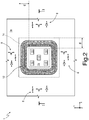
- Figure 2 illustrates the die of Figure 1 in top plan view, in the plane XY.
- the section view of Figure 1 is, in particular, taken along the line of section I-I of Figure 2 .
- the thermal-insulation region 1c extends so as to completely surround the power region 1b.
- the peripheral region 1a extends so that it completely surrounds the thermal-insulation region 1c.
- the function of the thermal-insulation region 1c is, as has been said, that of providing an obstacle for the propagation or transfer of the heat generated, during use, in the power region 1b, towards the peripheral region 1a. It is evident that, in the case where the peripheral region 1a extends facing part of the power region 1b (i.e., it does not surround it completely), the thermal-insulation region 1c can extend between the peripheral region 1a and the power region 1b, without surrounding the latter completely.
- the heat generated at the power region 1b is intercepted by the trenches 12 of the thermal-insulation region 1c.
- the one or more trenches 12 include a first filling layer 12a of dielectric material (e.g., SiO 2 ) and a second filling layer 12b, completely contained within the first filling layer 12a, made of a material adapted to compensate for the thermal stress that, in use, is generated at the trenches 12.
- a first filling layer 12a of dielectric material e.g., SiO 2
- a second filling layer 12b completely contained within the first filling layer 12a, made of a material adapted to compensate for the thermal stress that, in use, is generated at the trenches 12.
- the filling layer 12a may be subject to physical damage.
- Use of the second filling layer 12b, here polysilicon enables this undesired phenomenon to be overcome.
- the second filling layer 12b may be omitted in the case where the structural body 3 and the first filling layer 12a are made of materials such that the undesired phenomenon mentioned above is not present. Moreover, irrespectively of the materials used, the second filling layer 12b may be omitted also in the case where the specific operating application of the die 1 is such that no thermal stress is generated such as to cause damage to the trenches 12.
- the first filling layer 12a is made of a thermally insulating material, i.e., a material having a thermal conductivity approximately equal to 1 W/mK.
- the trenches 12 extend in depth in the structural body 3, starting from the top face 4a of the epitaxial layer 4, completely through the epitaxial layer 4 and through part of the substrate 2, terminating within the substrate 2.
- This embodiment presents the advantage of forming the trenches 12 simultaneously with trench regions for electrical insulation between devices/components in the peripheral region 1a.
- it is known to electrically insulate electronic components from one another, for example transistors, by means of trenches filled with dielectric material.
- the step of forming such electrical-insulation trenches further comprises the simultaneous step of forming the thermal-insulation trenches 12. The manufacturing costs are thus reduced, and the production process is speeded up.
- the trenches 12 may be formed in a separate step.
- the depth of the trenches 12 is not constrained to the depth of the trenches present in the peripheral region 1a.
- the trenches 12 may extend through just the thickness of the epitaxial layer 4 or, in general, terminate at the front side 2a of the substrate 2.
- one or more of the trenches 12 may extend throughout the entire thickness of the structural body 3, i.e., completely through the epitaxial layer 4 and through the substrate 2 until reaching the back side 2b of the substrate 2.
- the arrow T1 in Figure 1 identifies a direction of vertical propagation, along the direction of the axis Z, towards the back side 2b of the substrate 2.
- a first direction of lateral propagation, along the axis X indicated by the arrow T2.
- This heat propagation in the direction T2 is hindered by the presence of the trenches 12.
- a second lateral direction of propagation, along the axis X is indicated by the arrow T3, through the substrate 2 in the region of the latter without the trenches 12.
- the thermal-insulation region 1c has a lateral extension d, along the direction of the axis X, such that the thermal path T3 will have a greater distance than the thermal path T1.
- a value of d greater than the value of h where h is, as has been said, the thickness of the structural body 3.
- the lateral extension d is given, more in particular, by the sum of the extensions, along X, of each trench 12 plus the extension, once again along X, of the portion of the structural body 3 ranging between one trench 12 and the adjacent trench 12.
- the number, the material and lateral extension of the trenches 12 are also chosen so that the trenches 12 will offer an adequate thermal insulation in regard to the thermal wave T2, i.e., such that the heat propagating through them along the direction of the axis X (arrows T2') as far as the peripheral region 1a, will be lower than a threshold pre-set in the design step.
- the design of the trenches 12 may be performed by means of simulation programs, in a way in itself evident to the person skilled in the art.
- the trenches 12 hence delimit a path, or channel, of preferential propagation of the heat that is generated in the power region 1b, which hence propagates preferentially towards the back side 2b of the substrate 2.
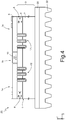
- the die 1 is coupled, during packaging, to a base plate 20 made of thermally conductive material, in particular metal material such as copper, of a package 25 (only a portion of the package 25 is illustrated in Figure 4 ).
- the base plate 20 of the package 25 is adapted to support the die 1 and is made of thermally conductive material to favour dissipation of the heat generated, in use, by the power devices 10.
- the base plate 20 is thermally coupled to a heat dissipater 22.
- the heat that propagates along T1 is transferred to the base plate 20 of the package 25 and then dissipated by means of the heat dissipater 22.
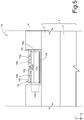
- FIG. 5 illustrates an enlarged detail of the power region 1b of the die 1.
- the power devices here in particular only a GaN-based HEMT device 10 is illustrated
- the device 10 includes a heterostructure 10a formed by a channel layer 10b, extending on which is a barrier layer 10c, made of aluminium and gallium nitride (AlGaN).
- An insulation layer 10d, made of dielectric material, extends on the barrier layer 10c.
- a gate terminal 10e extends on the barrier layer 10c between a source terminal 10f and a drain terminal 10g.
- the interface layer 26 has the function of forming an interface for lattice adaptation between the crystal lattice of the epitaxial layer 4 (which is here made of silicon) and the crystal lattice of the channel layer 10b (which is here made of GaN), and likewise has the function of favouring thermal coupling between the HEMT device 10 and the underlying structural body 3.
- the HEMT device 10 is of a lateral-conduction type, and has the source terminal 10f, the drain terminal 10g, and the gate terminal 10e on its top side, to favour their electrical contact (e.g., via wire bonding), for biasing of the device.
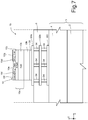
- the one or more power devices 10 are coupled to the structural body 3 of the die 1 following upon manufacturing of the peripheral components 8 (in Figure 6 just one single GaN-based HEMT device 10 is once again illustrated).
- the HEMT device 10 has a substrate 10h, made, for example, of Si or SiC, on which the heterostructure 10a extends.
- the dielectric layer 6 houses a plurality of metal layers 32a-32c, which form as a whole a metal stack.
- Figure 7 illustrates, by way of example, a bottom layer 32c, a top layer 32a, and an intermediate layer 32b, arranged between the bottom layer 32c and the top layer 32a.
- the metal layers 32a-32c are coupled together by means of thermally conductive through vias 34.
- the bottom metal layer 32c is in thermal contact with the structural body 3 (possibly via an interface layer), whereas the top metal layer 32a is in thermal contact with the substrate 10h of the device 10, via the coupling region 30 (here for instance, made of solder paste, for example lead or tin).
- the metal layers 32a-32c further improve thermal coupling between the HEMT device 10 and the structural body 3.
- Other coupling or bonding techniques between the HEMT device 10 and the structural body 3 may be used, as is evident to the person skilled in the art.
- the present invention enables thermal decoupling of the low-power (CMOS) circuitry from the high-power circuitry. It is thus possible to increase the density of integration of the components on a single die without incurring malfunctioning due to the high level of heat generated, in use, by the power devices.
- CMOS low-power
- the power devices housed in the power region 1b include one or more of the following: lateral (LDMOSs), BJTs, power MOSs (for example, bases on SiC), IGBTs, etc.
- LDMOSs lateral
- BJTs power MOSs (for example, bases on SiC)
- IGBTs IGBTs
- the components/circuits of the peripheral region 1a and of the power region 1b may form, together, an AC/AC cycloconverter, a DC/AC inverter, and an AC/DC rectifier.
Landscapes
- Engineering & Computer Science (AREA)
- General Engineering & Computer Science (AREA)
- Mechanical Engineering (AREA)
- Semiconductor Integrated Circuits (AREA)
- Manufacturing & Machinery (AREA)
- Chemical & Material Sciences (AREA)
- Crystallography & Structural Chemistry (AREA)
- Internal Circuitry In Semiconductor Integrated Circuit Devices (AREA)
- Metal-Oxide And Bipolar Metal-Oxide Semiconductor Integrated Circuits (AREA)
- Coupling Device And Connection With Printed Circuit (AREA)
- Cooling Or The Like Of Semiconductors Or Solid State Devices (AREA)
Abstract
Description
- The present invention relates to a semiconductor die, a method of manufacturing the semiconductor die, and a package housing the semiconductor die.
- GaN-based semiconductor devices are attracting considerable attention for power-electronics applications on account of their properties, such as the high breakdown electrical field, the high carrier density, the high electron mobility, and the high saturation rate. There are, on the other hand, known technologies for implementation of smart power integrated circuits (smart power ICs), based upon GaN-on-Silicon (GaN-on-Si) platforms having large dimensions, low cost, and high scalability.
- Currently, high-voltage power components (e.g., power transistors, GaN-based HEMT devices, etc.) are manufactured on, or bonded to, chips that house low-voltage peripheral devices and that form mixed digital/analog circuits. In particular, analog functional blocks, such as reference-voltage generators, voltage comparators, and voltage converters, have been obtained exploiting GaN-based technology in association with a peripheral circuitry obtained with CMOS silicon technology.
- In the aforementioned technical solutions, the peripheral circuitry has, for example, the function of protection and/or control of the power components, and is necessary for guaranteeing a robust control, a greater functionality, and greater reliability of the high-voltage power components (for example, against harmful operating conditions, as in the case of over-currents and overvoltages).
- It is highly desirable to integrate power devices in the same chip that houses the peripheral functional blocks, thus increasing the density of integration as far as possible.
- However, the performance of the peripheral circuits, as likewise those of power devices, are dependent upon temperature. An excessively high temperature, generated by the power devices, may cause malfunctioning of the peripheral circuitry or, in extreme conditions, burning-out of the chip or of parts thereof.
- Solutions for managing the temperature at a circuit level have been proposed (e.g., overtemperature protection circuits); likewise, cooling solutions are known that envisage the use of heat dissipaters at the package level.
- The above solutions, however, are not satisfactory when the density of integration increases and the distances between the electronic power devices and the peripheral circuitry are smaller.
- The aim of the present invention is to provide a semiconductor die, a method of manufacturing the semiconductor die, and a package housing the semiconductor die that will overcome the limitations of the prior art.
- According to the present invention, a semiconductor die, a method of manufacturing the semiconductor die, and a package housing the semiconductor die are provided, as defined in the annexed claims.
- For a better understanding of the present invention, a preferred embodiment thereof is now described, purely by way of non-limiting example, with reference to the attached drawings, wherein:
-
Figure 1 is a cross-section view of a portion of a die provided with an electrical-insulation region between a power region and a peripheral region, taken along the line of section I-I ofFigure 2 , according to one embodiment of the present invention; -
Figure 2 is a top plan view of the die ofFigure 1 ; -
Figure 3 is a cross-section view of a portion of a die provided with an electrical-insulation region between a power region and a peripheral region, taken along the line of section I-I ofFigure 2 , according to a further embodiment of the present invention; -
Figure 4 illustrates a portion of a package housing the die ofFigure 1 orFigure 3 ; and -
Figures 5 to 7 are variations of manufacturing of the power region of the die ofFigure 1 orFigure 3 . -
Figure 1 illustrates, in a side section view in a triaxial cartesian reference system X, Y, Z, a portion of adie 1 according to an aspect of the present invention. The elements illustrated inFigure 1 are not represented in the same scale, but are represented schematically and by way of example, in order to facilitate understanding of the present invention. - The die 1 comprises: a
substrate 2, made of silicon (for example, silicon with a P-type doping), having afront side 2a and aback side 2b, opposite to each other along the direction of the axis Z; anepitaxial layer 4, made of epitaxially grown silicon (for example, with a N-type doping), which extends over thefront side 2a of thesubstrate 2; and adielectric layer 6, made, for example, of silicon oxide (SiO2), which extends over atop face 4a of theepitaxial layer 4. - It is evident that between the
substrate 2 and theepitaxial layer 4 further epitaxial layers, or layers of some other type (not illustrated) may be present. In what follows, the ensemble of thesubstrate 2 and theepitaxial layer 4, including said possible further layers if present, will be referred to as "structural body 3", which has a thickness, considered along the axis X between thetop face 4a of theepitaxial layer 4 and theback side 2b of thesubstrate 2, denoted by h. As will be more evident in the following description, the possible further layers present are of a thermally conductive material (indicatively, with a thermal conductivity comparable to, or higher than, that of the materials of thesubstrate 2 and/or of the epitaxial layer 4). - According to an aspect of the present invention, to enable a high density of integration, a planar process is used for the manufacturing of high-
voltage power devices 10 and of low-voltage peripheral devices 8 (e.g., obtained with CMOS technology) that implement functional blocks adapted to control/support operation of the power devices. - The layout of the
die 1 may be organised so as to group together, in one and the same region of thedie 1, the high-voltage power devices 10, and group together in one and the same respective region of thedie 1 the low-voltageperipheral devices 8. In particular, the low-voltageperipheral devices 8 are formed in a region that surrounds, in top plan view (in the plane XY), the region that houses the high-voltage power devices 10. - For this purpose, with reference to
Figures 1 and2 , the die 1 (more in particular, the structural body 3) comprises afirst region 1a that houses the low-voltage peripheral devices 8 (integrated in thestructural body 3, at least partly in the epitaxial layer 4). In what follows, thefirst region 1a will also be referred to as "peripheral region 1a", and the components housed therein will also be referred to as "peripheral components 8". Extending on thedielectric layer 6 are one or more electrical-contact pads 7, electrically coupled to theperipheral components 8 by means of conductive through vias and metal layers, generically designated by thereference number 9. - The die 1 (more in particular, the structural body 3) further comprises a
second region 1b that houses one or more high-voltage power devices 10, which include, for example, one or more GaN-based HEMTs. In general, the high-voltage power devices 10 dissipate, during use, thermal energy of the order of hundreds of microjoules. In what follows, thissecond region 1b will also be referred to as "power region 1b", and the high-voltage power devices 10 will also be referred to as "power devices 10". - By way of example, the components/circuits of the
peripheral region 1a and of thepower region 1b form, together, a DC/DC converter, where the components/circuits of theperipheral region 1a form the control part (e.g., pre-amplification circuits, driving circuit for biasing the gate terminal or terminals, etc.) of the DC/DC converter, whereas the power devices housed in thepower region 1b form the switch elements of the DC/DC converter. - The die 1 (more in particular, the structural body 3) further comprises a
third region 1c, which extends, in top plan view (i.e., in the plane XY), between thefirst region 1a and thesecond region 1b and houses one ormore trenches 12 adapted to form an obstacle for lateral thermal propagation of the heat generated, during use, by thepower devices 10 in thepower region 1b (as indicated in the figure by the arrows T2, which represent the propagation of heat in the direction X, intercepted and hindered by the trenches 12). In what follows, thethird region 1c will also be referred to as "thermal-insulation region 1c". -
Figure 2 illustrates the die ofFigure 1 in top plan view, in the plane XY. The section view ofFigure 1 is, in particular, taken along the line of section I-I ofFigure 2 . As may be noted fromFigure 2 , the thermal-insulation region 1c extends so as to completely surround thepower region 1b. In turn, theperipheral region 1a extends so that it completely surrounds the thermal-insulation region 1c. - The function of the thermal-
insulation region 1c is, as has been said, that of providing an obstacle for the propagation or transfer of the heat generated, during use, in thepower region 1b, towards theperipheral region 1a. It is evident that, in the case where theperipheral region 1a extends facing part of thepower region 1b (i.e., it does not surround it completely), the thermal-insulation region 1c can extend between theperipheral region 1a and thepower region 1b, without surrounding the latter completely. - In any direction of thermal propagation considered (i.e., along X, along Y, or in directions that have a component both along X and along Y), the heat generated at the
power region 1b is intercepted by thetrenches 12 of the thermal-insulation region 1c. - Returning to
Figure 1 , the one or more trenches 12 (here a plurality oftrenches 12 are illustrated by way of example) include afirst filling layer 12a of dielectric material (e.g., SiO2) and asecond filling layer 12b, completely contained within thefirst filling layer 12a, made of a material adapted to compensate for the thermal stress that, in use, is generated at thetrenches 12. The present applicant has in fact noted that, on account of the different thermal expansions of the silicon oxide of thefilling layer 12a with respect to the silicon of thestructural body 3, thefilling layer 12a may be subject to physical damage. Use of thesecond filling layer 12b, here polysilicon, enables this undesired phenomenon to be overcome. - It is, however, evident that, in the case where the
structural body 3 and thefirst filling layer 12a are made of materials such that the undesired phenomenon mentioned above is not present, thesecond filling layer 12b may be omitted. Moreover, irrespectively of the materials used, thesecond filling layer 12b may be omitted also in the case where the specific operating application of thedie 1 is such that no thermal stress is generated such as to cause damage to thetrenches 12. - In general, the
first filling layer 12a is made of a thermally insulating material, i.e., a material having a thermal conductivity approximately equal to 1 W/mK. - The
trenches 12 extend in depth in thestructural body 3, starting from thetop face 4a of theepitaxial layer 4, completely through theepitaxial layer 4 and through part of thesubstrate 2, terminating within thesubstrate 2. This embodiment presents the advantage of forming thetrenches 12 simultaneously with trench regions for electrical insulation between devices/components in theperipheral region 1a. In fact, it is known to electrically insulate electronic components from one another, for example transistors, by means of trenches filled with dielectric material. During processing of thedie 1, the step of forming such electrical-insulation trenches further comprises the simultaneous step of forming the thermal-insulation trenches 12. The manufacturing costs are thus reduced, and the production process is speeded up. - Alternatively it is, however, possible to form the
trenches 12 in a separate step. In this case, the depth of thetrenches 12 is not constrained to the depth of the trenches present in theperipheral region 1a. In particular, thetrenches 12 may extend through just the thickness of theepitaxial layer 4 or, in general, terminate at thefront side 2a of thesubstrate 2. - According to a further embodiment, illustrated in
Figure 3 , one or more of the trenches 12 (inFigure 3 , all of the trenches 12) may extend throughout the entire thickness of thestructural body 3, i.e., completely through theepitaxial layer 4 and through thesubstrate 2 until reaching theback side 2b of thesubstrate 2. - The heat generated, in use, in the
power region 1b propagates through thestructural body 3. Among the various possible directions of propagation, the arrow T1 inFigure 1 identifies a direction of vertical propagation, along the direction of the axis Z, towards theback side 2b of thesubstrate 2. Likewise identified inFigure 1 is a first direction of lateral propagation, along the axis X, indicated by the arrow T2. This heat propagation in the direction T2 is hindered by the presence of thetrenches 12. Furthermore, a second lateral direction of propagation, along the axis X, is indicated by the arrow T3, through thesubstrate 2 in the region of the latter without thetrenches 12. - The thermal-
insulation region 1c has a lateral extension d, along the direction of the axis X, such that the thermal path T3 will have a greater distance than the thermal path T1. To meet this requirement, in the design step, there is conservatively chosen a value of d greater than the value of h, where h is, as has been said, the thickness of thestructural body 3. The lateral extension d is given, more in particular, by the sum of the extensions, along X, of eachtrench 12 plus the extension, once again along X, of the portion of thestructural body 3 ranging between onetrench 12 and theadjacent trench 12. - The number, the material and lateral extension of the
trenches 12 are also chosen so that thetrenches 12 will offer an adequate thermal insulation in regard to the thermal wave T2, i.e., such that the heat propagating through them along the direction of the axis X (arrows T2') as far as theperipheral region 1a, will be lower than a threshold pre-set in the design step. - The design of the trenches 12 (for example, in terms of number of trenches, materials, and thicknesses of the filling layers, lateral extension of the trenches, etc.) may be performed by means of simulation programs, in a way in itself evident to the person skilled in the art.
- It is clear that what has been described above with particular reference to the direction of thermal propagation along X (in particular, with reference to the lateral extension d of the thermal-
insulation region 1c) applies to any direction of thermal propagation considered, i.e., along X, along Y, and in directions that have a component both along X and along Y. - The
trenches 12 hence delimit a path, or channel, of preferential propagation of the heat that is generated in thepower region 1b, which hence propagates preferentially towards theback side 2b of thesubstrate 2. - As illustrated schematically in
Figure 4 , thedie 1 is coupled, during packaging, to abase plate 20 made of thermally conductive material, in particular metal material such as copper, of a package 25 (only a portion of thepackage 25 is illustrated inFigure 4 ). Thebase plate 20 of thepackage 25 is adapted to support thedie 1 and is made of thermally conductive material to favour dissipation of the heat generated, in use, by thepower devices 10. Typically, thebase plate 20 is thermally coupled to aheat dissipater 22. - Hence, in use, the heat that propagates along T1, or that in general reaches the back side of the
substrate 2, is transferred to thebase plate 20 of thepackage 25 and then dissipated by means of theheat dissipater 22. -
Figure 5 illustrates an enlarged detail of thepower region 1b of thedie 1. In this embodiment, the power devices (here in particular only a GaN-basedHEMT device 10 is illustrated) are formed on thestructural body 3 in manufacturing steps that are simultaneous or subsequent to the manufacturing steps of theperipheral components 8. Manufacture of a GaN-based HEMT device is in itself known and not described herein in so far as it does not form the subject of the present invention. Thedevice 10 includes aheterostructure 10a formed by achannel layer 10b, extending on which is abarrier layer 10c, made of aluminium and gallium nitride (AlGaN). Aninsulation layer 10d, made of dielectric material, extends on thebarrier layer 10c. Agate terminal 10e extends on thebarrier layer 10c between asource terminal 10f and adrain terminal 10g. - To favour adhesion of the
channel layer 10b of thedevice 10 to thestructural body 3 of thedie 1 aninterface layer 26 made of aluminium nitride is present. Theinterface layer 26 has the function of forming an interface for lattice adaptation between the crystal lattice of the epitaxial layer 4 (which is here made of silicon) and the crystal lattice of thechannel layer 10b (which is here made of GaN), and likewise has the function of favouring thermal coupling between theHEMT device 10 and the underlyingstructural body 3. - The
HEMT device 10 is of a lateral-conduction type, and has thesource terminal 10f, thedrain terminal 10g, and thegate terminal 10e on its top side, to favour their electrical contact (e.g., via wire bonding), for biasing of the device. - In a different embodiment, illustrated in
Figure 6 in the same enlarged view as that ofFigure 5 , the one ormore power devices 10 are coupled to thestructural body 3 of thedie 1 following upon manufacturing of the peripheral components 8 (inFigure 6 just one single GaN-basedHEMT device 10 is once again illustrated). - In this case, the
HEMT device 10 has asubstrate 10h, made, for example, of Si or SiC, on which theheterostructure 10a extends. A thermallyconductive coupling region 30, for example made of thermally conductive glue or solder paste, which extends between thesubstrate 10h of theHEMT device 10 and thestructural body 3, coupling them together. - According to a further embodiment, illustrated in
Figure 7 , thedielectric layer 6 houses a plurality ofmetal layers 32a-32c, which form as a whole a metal stack.Figure 7 illustrates, by way of example, abottom layer 32c, atop layer 32a, and anintermediate layer 32b, arranged between thebottom layer 32c and thetop layer 32a. The metal layers 32a-32c are coupled together by means of thermally conductive throughvias 34. Thebottom metal layer 32c is in thermal contact with the structural body 3 (possibly via an interface layer), whereas thetop metal layer 32a is in thermal contact with thesubstrate 10h of thedevice 10, via the coupling region 30 (here for instance, made of solder paste, for example lead or tin). The metal layers 32a-32c further improve thermal coupling between theHEMT device 10 and thestructural body 3. Other coupling or bonding techniques between theHEMT device 10 and thestructural body 3 may be used, as is evident to the person skilled in the art. - From an examination of the characteristics of the present invention provided according to the present disclosure, the advantages that it affords are evident.
- In particular, the present invention enables thermal decoupling of the low-power (CMOS) circuitry from the high-power circuitry. It is thus possible to increase the density of integration of the components on a single die without incurring malfunctioning due to the high level of heat generated, in use, by the power devices.
- Finally, it is clear that modifications and variations may be made to the invention described and illustrated herein, without thereby departing from the scope thereof, as defined in the annexed claims.
- For instance, the power devices housed in the
power region 1b include one or more of the following: lateral (LDMOSs), BJTs, power MOSs (for example, bases on SiC), IGBTs, etc. - Moreover, the components/circuits of the
peripheral region 1a and of thepower region 1b may form, together, an AC/AC cycloconverter, a DC/AC inverter, and an AC/DC rectifier.
Claims (19)
- A semiconductor die (1) including:- a structural body (3) made of semiconductor material having a front side (4a) and a back side (2b), the back side (2b) being coupleable to a base plate (20) of a package (25), the structural body (3) including a first region (1b) and a second region (1a), which surrounds, in top plan view, the first region (1b); and- at least one semiconductor power device (10), which is arranged in the first region (1b) at the front side (4a) of the structural body (3) and is coupled to the structural body (3) by means of a thermally conductive coupling interface (26; 30; 32),characterised by further comprising trench-insulation means (12), which extend in the structural body (3) starting from the front side (4a) towards the back side (2b) along a first direction (Z),
wherein the trench-insulation means (12) surround and delimit the first region (1b) and have dimensions and are made of materials such as to form an obstacle to heat conduction from the first region (1b) towards the second region (1a) along a second direction (X) orthogonal to the first direction (Z) . - The semiconductor die according to claim 1, wherein the trench-insulation means (12) have an extension (d), in said second direction (X), greater than the thickness (h) of the structural body (3) measured along the first direction (Z) from the front side to the back side.
- The semiconductor die according to claim 1 or 2, wherein the trench-insulation means (12) comprise, alternatively:(i) a plurality of trenches in succession with one another along the second direction (X) and spaced apart from one another, along the second direction (X), by a respective separation region, said extension (d) of the trench-insulation means (12) being the sum of the extensions of each trench and of the respective separation portions in the second direction (X); or(ii) a single trench, said extension (d) of the trench-insulation means (12) being the extension, along the second direction (X), of said single trench.
- The semiconductor die according to claim 3, wherein each trench of the plurality of trenches, or said single trench, includes thermally insulating material.
- The semiconductor die according to claim 3 or 4, wherein each trench of the plurality of trenches, or said single trench, includes a respective layer of dielectric material (12a) and a respective polysilicon region (12b), each layer of dielectric material (12a) completely surrounding the respective polysilicon region (12b).
- The semiconductor die according to any one of the preceding claims, wherein said trench-insulation means extend, along the first direction (Z), through the entire structural body (3) as far as the back side (2b).
- The semiconductor die according to any one of the preceding claims, wherein said trench-insulation means (12) extend, along the first direction (Z), through part of the thickness of the structural body (3), terminating inside the structural body (3).
- The semiconductor die according to claim 7, wherein the structural body (3) includes a substrate (2), made of P-type silicon, and an epitaxial layer (4), made of N-type silicon, which extends over the substrate (2),
said trench-insulation means extending completely through the epitaxial layer (4), terminating inside the substrate (2). - The semiconductor die according to any one of the preceding claims, wherein said coupling interface (26; 30; 32) comprises one of the following: a layer of aluminium nitride, thermally conductive glue, solder paste, and a metal stack.
- The semiconductor die according to any one of the preceding claims, wherein said peripheral region (1a) comprises a plurality of electronic components manufactured with CMOS technology.
- The semiconductor die according to any one of the preceding claims, wherein said at least one semiconductor power device (10) is a GaN-based HEMT device.
- The semiconductor die according to any one of the preceding claims, wherein the trench-insulation means (12) completely surround, in top plan view, the first region (1b), to form a ring-like thermal-insulation structure.
- A method of manufacturing a semiconductor die (1) including the steps of:- providing a structural body (3) of semiconductor material having a front side (4a) and a back side (2b), the back side (2b) being coupleable to a base plate (20) of a package (25), the structural body (3) including a first region (1b) and a second region (1a) surrounding, in top plan view, the first region (1b); and- coupling at least one semiconductor power device (10) on the front side (4a) of the structural body (3), in the first region (1b), by means of a thermally conductive coupling interface,characterised in that it further comprises the step of forming, in the structural body (3), trench-insulation means (12), which extend along a first direction (Z) starting from the front side (4a) towards the back side (2b),
wherein the trench-insulation means (12) are formed so as to surround and delimit the first region (1b) and have dimensions and are made of materials chosen so as to form an obstacle to the conduction of heat from the first region (1b) towards the second region (1a) along a second direction (X) orthogonal to the first direction (Z). - The method according to claim 13, wherein the step of forming the trench-insulation means (12) comprises forming the trench-insulation means (12) so that they have an extension (d), along said second direction (X), greater than the thickness (h) of the structural body (3) measured along the first direction (Z) from the front side to the back side.
- The method according to claim 13 or 14, wherein the step of coupling said at least one semiconductor power device (10) includes forming said coupling interface (26; 30; 32) and forming, on said coupling interface, said semiconductor power device (10).
- The method according to claim 13 or 14, wherein the step of coupling said at least one semiconductor power device (10) includes forming said coupling interface (26; 30; 32) of thermally conductive glue or solder paste, and mounting said semiconductor power device (10) on the coupling interface.
- The method according to any one of the claims 13 to 16, wherein the step of forming the trench-insulation means (12) comprises, alternatively:(i) forming a plurality of mutually successive trenches along the second direction (X) spaced apart from one another by a respective separation region, said extension (d) of the trench-insulation means (12) being the sum of the extensions of each trench and of the respective separation portions along the second direction (X); or(ii) forming a single trench, said extension (d) of the trench-insulation means (12) being the extension, along the second direction (X), of said single trench.
- The method according to claim 17, wherein the step of forming each trench of the plurality of trenches, or the step of forming said single trench, includes etching selective portions of the semiconductor body on the front side (4a) and depositing thermally insulating material.
- A package (25), comprising:- a base plate (20), made of thermally conductive material; and- a semiconductor die according to any one of claims 1 to 12, thermally coupled to the base plate (20).
Applications Claiming Priority (1)
| Application Number | Priority Date | Filing Date | Title |
|---|---|---|---|
| IT102019000001201A IT201900001201A1 (en) | 2019-01-28 | 2019-01-28 | SEMICONDUCTOR PLATE WITH IMPROVED THERMAL INSULATION BETWEEN A POWER PORTION AND A PERIPHERAL PORTION, MANUFACTURING METHOD, AND PACKAGE HOUSING THE PLATE |
Publications (2)
| Publication Number | Publication Date |
|---|---|
| EP3686923A1 true EP3686923A1 (en) | 2020-07-29 |
| EP3686923B1 EP3686923B1 (en) | 2025-07-02 |
Family
ID=66049624
Family Applications (1)
| Application Number | Title | Priority Date | Filing Date |
|---|---|---|---|
| EP20154200.8A Active EP3686923B1 (en) | 2019-01-28 | 2020-01-28 | Semiconductor die with improved thermal insulation between a power portion and a peripheral portion, method of manufacturing, and package housing the die |
Country Status (4)
| Country | Link |
|---|---|
| US (3) | US11063027B2 (en) |
| EP (1) | EP3686923B1 (en) |
| CN (2) | CN211376620U (en) |
| IT (1) | IT201900001201A1 (en) |
Families Citing this family (3)
| Publication number | Priority date | Publication date | Assignee | Title |
|---|---|---|---|---|
| IT201900001201A1 (en) * | 2019-01-28 | 2020-07-28 | St Microelectronics Srl | SEMICONDUCTOR PLATE WITH IMPROVED THERMAL INSULATION BETWEEN A POWER PORTION AND A PERIPHERAL PORTION, MANUFACTURING METHOD, AND PACKAGE HOUSING THE PLATE |
| CN116780331A (en) * | 2022-03-10 | 2023-09-19 | 浙江睿熙科技有限公司 | VCSEL chip and preparation method thereof |
| CN219017637U (en) * | 2022-08-03 | 2023-05-12 | 苏州晶湛半导体有限公司 | Composite substrate and semiconductor structure |
Citations (5)
| Publication number | Priority date | Publication date | Assignee | Title |
|---|---|---|---|---|
| US20040021198A1 (en) * | 2002-08-01 | 2004-02-05 | Ting-Wah Wong | Isolating temperature sensitive components from heat sources in integrated circuits |
| US20080006913A1 (en) * | 2006-07-07 | 2008-01-10 | Infineon Technologies Austria Ag | Integrated semiconductor chip with lateral thermal insulation |
| US20090279218A1 (en) * | 2006-04-20 | 2009-11-12 | Nxp B.V. | Thermal isolation of electronic devices in submount used for leds lighting applications |
| US20170256638A1 (en) * | 2016-03-03 | 2017-09-07 | Gan Systems Inc. | GaN-on-Si SEMICONDUCTOR DEVICE STRUCTURES FOR HIGH CURRENT/ HIGH VOLTAGE LATERAL GaN TRANSISTORS AND METHODS OF FABRICATION THEREOF |
| US9761543B1 (en) * | 2016-12-20 | 2017-09-12 | Texas Instruments Incorporated | Integrated circuits with thermal isolation and temperature regulation |
Family Cites Families (6)
| Publication number | Priority date | Publication date | Assignee | Title |
|---|---|---|---|---|
| JP2005136311A (en) * | 2003-10-31 | 2005-05-26 | Matsushita Electric Ind Co Ltd | Nitride semiconductor substrate and manufacturing method thereof |
| JP5061597B2 (en) * | 2006-11-24 | 2012-10-31 | トヨタ自動車株式会社 | Semiconductor device |
| EP2567404B1 (en) * | 2010-05-02 | 2017-07-12 | Visic Technologies Ltd. | Field effect power transistors |
| US9281359B2 (en) * | 2012-08-20 | 2016-03-08 | Infineon Technologies Ag | Semiconductor device comprising contact trenches |
| TWI571959B (en) * | 2014-09-02 | 2017-02-21 | 萬國半導體股份有限公司 | Power trench mosfet with mproved uis performance and preparation method thereof |
| IT201900001201A1 (en) * | 2019-01-28 | 2020-07-28 | St Microelectronics Srl | SEMICONDUCTOR PLATE WITH IMPROVED THERMAL INSULATION BETWEEN A POWER PORTION AND A PERIPHERAL PORTION, MANUFACTURING METHOD, AND PACKAGE HOUSING THE PLATE |
-
2019
- 2019-01-28 IT IT102019000001201A patent/IT201900001201A1/en unknown
-
2020
- 2020-01-23 CN CN202020146399.5U patent/CN211376620U/en active Active
- 2020-01-23 CN CN202010076684.9A patent/CN111490016B/en active Active
- 2020-01-27 US US16/773,711 patent/US11063027B2/en active Active
- 2020-01-28 EP EP20154200.8A patent/EP3686923B1/en active Active
-
2021
- 2021-06-22 US US17/354,448 patent/US11569211B2/en active Active
-
2022
- 2022-12-28 US US18/147,563 patent/US11948927B2/en active Active
Patent Citations (5)
| Publication number | Priority date | Publication date | Assignee | Title |
|---|---|---|---|---|
| US20040021198A1 (en) * | 2002-08-01 | 2004-02-05 | Ting-Wah Wong | Isolating temperature sensitive components from heat sources in integrated circuits |
| US20090279218A1 (en) * | 2006-04-20 | 2009-11-12 | Nxp B.V. | Thermal isolation of electronic devices in submount used for leds lighting applications |
| US20080006913A1 (en) * | 2006-07-07 | 2008-01-10 | Infineon Technologies Austria Ag | Integrated semiconductor chip with lateral thermal insulation |
| US20170256638A1 (en) * | 2016-03-03 | 2017-09-07 | Gan Systems Inc. | GaN-on-Si SEMICONDUCTOR DEVICE STRUCTURES FOR HIGH CURRENT/ HIGH VOLTAGE LATERAL GaN TRANSISTORS AND METHODS OF FABRICATION THEREOF |
| US9761543B1 (en) * | 2016-12-20 | 2017-09-12 | Texas Instruments Incorporated | Integrated circuits with thermal isolation and temperature regulation |
Also Published As
| Publication number | Publication date |
|---|---|
| US20200243496A1 (en) | 2020-07-30 |
| US11569211B2 (en) | 2023-01-31 |
| US11948927B2 (en) | 2024-04-02 |
| CN111490016B (en) | 2025-09-26 |
| EP3686923B1 (en) | 2025-07-02 |
| CN211376620U (en) | 2020-08-28 |
| US20210375839A1 (en) | 2021-12-02 |
| US11063027B2 (en) | 2021-07-13 |
| US20230187425A1 (en) | 2023-06-15 |
| IT201900001201A1 (en) | 2020-07-28 |
| CN111490016A (en) | 2020-08-04 |
Similar Documents
| Publication | Publication Date | Title |
|---|---|---|
| US20240339421A1 (en) | Electronic component and semiconductor device | |
| US11948927B2 (en) | Semiconductor die with improved thermal insulation between a power portion and a peripheral portion, method of manufacturing, and package housing the die | |
| JP5319084B2 (en) | Semiconductor device | |
| TWI755485B (en) | Integrated circuit package apparatus and integrated circuit packaging method for minimizing crosstalk | |
| CN102439713B (en) | Bumped, self-isolated GaN transistor chip with electrically isolated back surface | |
| US9536803B2 (en) | Integrated power module with improved isolation and thermal conductivity | |
| CN102005441A (en) | Semiconductor switching device with controllable hybrid package gate and its preparation method | |
| US10051742B2 (en) | Power module and manufacturing method thereof | |
| CN104009085A (en) | Through hole and method for forming same | |
| JP2025029152A (en) | Electronic device flip chip package with exposed clips - Patents.com | |
| EP2639832A2 (en) | Group III-V and group IV composite diode | |
| EP2521172A1 (en) | High voltage cascoded III-nitride rectifier package with etched leadframe | |
| US20110180855A1 (en) | Non-direct bond copper isolated lateral wide band gap semiconductor device | |
| JP2010010434A (en) | Semiconductor device and semiconductor module | |
| Lee et al. | A new package of high-voltage cascode gallium nitride device for high-frequency applications | |
| CN102074539A (en) | Package for semiconductor devices | |
| CN108063127B (en) | Chips and power transistors | |
| EP4495990A1 (en) | Semiconductor substrate, semiconductor component and methods | |
| CN223566612U (en) | A GaN chip packaging structure and electronic device |
Legal Events
| Date | Code | Title | Description |
|---|---|---|---|
| PUAI | Public reference made under article 153(3) epc to a published international application that has entered the european phase |
Free format text: ORIGINAL CODE: 0009012 |
|
| STAA | Information on the status of an ep patent application or granted ep patent |
Free format text: STATUS: THE APPLICATION HAS BEEN PUBLISHED |
|
| AK | Designated contracting states |
Kind code of ref document: A1 Designated state(s): AL AT BE BG CH CY CZ DE DK EE ES FI FR GB GR HR HU IE IS IT LI LT LU LV MC MK MT NL NO PL PT RO RS SE SI SK SM TR |
|
| AX | Request for extension of the european patent |
Extension state: BA ME |
|
| STAA | Information on the status of an ep patent application or granted ep patent |
Free format text: STATUS: REQUEST FOR EXAMINATION WAS MADE |
|
| 17P | Request for examination filed |
Effective date: 20201201 |
|
| RBV | Designated contracting states (corrected) |
Designated state(s): AL AT BE BG CH CY CZ DE DK EE ES FI FR GB GR HR HU IE IS IT LI LT LU LV MC MK MT NL NO PL PT RO RS SE SI SK SM TR |
|
| STAA | Information on the status of an ep patent application or granted ep patent |
Free format text: STATUS: EXAMINATION IS IN PROGRESS |
|
| 17Q | First examination report despatched |
Effective date: 20211103 |
|
| GRAP | Despatch of communication of intention to grant a patent |
Free format text: ORIGINAL CODE: EPIDOSNIGR1 |
|
| STAA | Information on the status of an ep patent application or granted ep patent |
Free format text: STATUS: GRANT OF PATENT IS INTENDED |
|
| RIC1 | Information provided on ipc code assigned before grant |
Ipc: H10D 84/02 20250101ALN20250123BHEP Ipc: H10D 89/10 20250101ALI20250123BHEP Ipc: H10D 84/08 20250101ALI20250123BHEP Ipc: H01L 23/367 20060101ALI20250123BHEP Ipc: H10D 84/00 20250101ALI20250123BHEP Ipc: H01L 21/762 20060101AFI20250123BHEP |
|
| INTG | Intention to grant announced |
Effective date: 20250204 |
|
| RIC1 | Information provided on ipc code assigned before grant |
Ipc: H10D 84/02 20250101ALN20250128BHEP Ipc: H10D 89/10 20250101ALI20250128BHEP Ipc: H10D 84/08 20250101ALI20250128BHEP Ipc: H01L 23/367 20060101ALI20250128BHEP Ipc: H10D 84/00 20250101ALI20250128BHEP Ipc: H01L 21/762 20060101AFI20250128BHEP |
|
| GRAS | Grant fee paid |
Free format text: ORIGINAL CODE: EPIDOSNIGR3 |
|
| GRAA | (expected) grant |
Free format text: ORIGINAL CODE: 0009210 |
|
| STAA | Information on the status of an ep patent application or granted ep patent |
Free format text: STATUS: THE PATENT HAS BEEN GRANTED |
|
| AK | Designated contracting states |
Kind code of ref document: B1 Designated state(s): AL AT BE BG CH CY CZ DE DK EE ES FI FR GB GR HR HU IE IS IT LI LT LU LV MC MK MT NL NO PL PT RO RS SE SI SK SM TR |
|
| REG | Reference to a national code |
Ref country code: GB Ref legal event code: FG4D |
|
| REG | Reference to a national code |
Ref country code: CH Ref legal event code: EP |
|
| REG | Reference to a national code |
Ref country code: DE Ref legal event code: R096 Ref document number: 602020053620 Country of ref document: DE |
|
| REG | Reference to a national code |
Ref country code: IE Ref legal event code: FG4D |
|
| REG | Reference to a national code |
Ref country code: NL Ref legal event code: MP Effective date: 20250702 |
|
| REG | Reference to a national code |
Ref country code: DE Ref legal event code: R079 Ref document number: 602020053620 Country of ref document: DE Free format text: PREVIOUS MAIN CLASS: H01L0021762000 Ipc: H10W0010100000 |
|
| PG25 | Lapsed in a contracting state [announced via postgrant information from national office to epo] |
Ref country code: PT Free format text: LAPSE BECAUSE OF FAILURE TO SUBMIT A TRANSLATION OF THE DESCRIPTION OR TO PAY THE FEE WITHIN THE PRESCRIBED TIME-LIMIT Effective date: 20251103 |
|
| PG25 | Lapsed in a contracting state [announced via postgrant information from national office to epo] |
Ref country code: NL Free format text: LAPSE BECAUSE OF FAILURE TO SUBMIT A TRANSLATION OF THE DESCRIPTION OR TO PAY THE FEE WITHIN THE PRESCRIBED TIME-LIMIT Effective date: 20250702 |
|
| REG | Reference to a national code |
Ref country code: AT Ref legal event code: MK05 Ref document number: 1810280 Country of ref document: AT Kind code of ref document: T Effective date: 20250702 |
|
| PG25 | Lapsed in a contracting state [announced via postgrant information from national office to epo] |
Ref country code: IS Free format text: LAPSE BECAUSE OF FAILURE TO SUBMIT A TRANSLATION OF THE DESCRIPTION OR TO PAY THE FEE WITHIN THE PRESCRIBED TIME-LIMIT Effective date: 20251102 |
|
| PG25 | Lapsed in a contracting state [announced via postgrant information from national office to epo] |
Ref country code: NO Free format text: LAPSE BECAUSE OF FAILURE TO SUBMIT A TRANSLATION OF THE DESCRIPTION OR TO PAY THE FEE WITHIN THE PRESCRIBED TIME-LIMIT Effective date: 20251002 |
|
| REG | Reference to a national code |
Ref country code: LT Ref legal event code: MG9D |
|
| PG25 | Lapsed in a contracting state [announced via postgrant information from national office to epo] |
Ref country code: AT Free format text: LAPSE BECAUSE OF FAILURE TO SUBMIT A TRANSLATION OF THE DESCRIPTION OR TO PAY THE FEE WITHIN THE PRESCRIBED TIME-LIMIT Effective date: 20250702 |
|
| PG25 | Lapsed in a contracting state [announced via postgrant information from national office to epo] |
Ref country code: FI Free format text: LAPSE BECAUSE OF FAILURE TO SUBMIT A TRANSLATION OF THE DESCRIPTION OR TO PAY THE FEE WITHIN THE PRESCRIBED TIME-LIMIT Effective date: 20250702 |
|
| PG25 | Lapsed in a contracting state [announced via postgrant information from national office to epo] |
Ref country code: HR Free format text: LAPSE BECAUSE OF FAILURE TO SUBMIT A TRANSLATION OF THE DESCRIPTION OR TO PAY THE FEE WITHIN THE PRESCRIBED TIME-LIMIT Effective date: 20250702 |
|
| PG25 | Lapsed in a contracting state [announced via postgrant information from national office to epo] |
Ref country code: GR Free format text: LAPSE BECAUSE OF FAILURE TO SUBMIT A TRANSLATION OF THE DESCRIPTION OR TO PAY THE FEE WITHIN THE PRESCRIBED TIME-LIMIT Effective date: 20251003 |
|
| PG25 | Lapsed in a contracting state [announced via postgrant information from national office to epo] |
Ref country code: CZ Free format text: LAPSE BECAUSE OF FAILURE TO SUBMIT A TRANSLATION OF THE DESCRIPTION OR TO PAY THE FEE WITHIN THE PRESCRIBED TIME-LIMIT Effective date: 20250702 Ref country code: SE Free format text: LAPSE BECAUSE OF FAILURE TO SUBMIT A TRANSLATION OF THE DESCRIPTION OR TO PAY THE FEE WITHIN THE PRESCRIBED TIME-LIMIT Effective date: 20250702 |
|
| PG25 | Lapsed in a contracting state [announced via postgrant information from national office to epo] |
Ref country code: LV Free format text: LAPSE BECAUSE OF FAILURE TO SUBMIT A TRANSLATION OF THE DESCRIPTION OR TO PAY THE FEE WITHIN THE PRESCRIBED TIME-LIMIT Effective date: 20250702 |
|
| PG25 | Lapsed in a contracting state [announced via postgrant information from national office to epo] |
Ref country code: BG Free format text: LAPSE BECAUSE OF FAILURE TO SUBMIT A TRANSLATION OF THE DESCRIPTION OR TO PAY THE FEE WITHIN THE PRESCRIBED TIME-LIMIT Effective date: 20250702 Ref country code: PL Free format text: LAPSE BECAUSE OF FAILURE TO SUBMIT A TRANSLATION OF THE DESCRIPTION OR TO PAY THE FEE WITHIN THE PRESCRIBED TIME-LIMIT Effective date: 20250702 |
|
| PG25 | Lapsed in a contracting state [announced via postgrant information from national office to epo] |
Ref country code: RS Free format text: LAPSE BECAUSE OF FAILURE TO SUBMIT A TRANSLATION OF THE DESCRIPTION OR TO PAY THE FEE WITHIN THE PRESCRIBED TIME-LIMIT Effective date: 20251002 |
|
| PG25 | Lapsed in a contracting state [announced via postgrant information from national office to epo] |
Ref country code: ES Free format text: LAPSE BECAUSE OF FAILURE TO SUBMIT A TRANSLATION OF THE DESCRIPTION OR TO PAY THE FEE WITHIN THE PRESCRIBED TIME-LIMIT Effective date: 20250702 |
|
| PG25 | Lapsed in a contracting state [announced via postgrant information from national office to epo] |
Ref country code: SM Free format text: LAPSE BECAUSE OF FAILURE TO SUBMIT A TRANSLATION OF THE DESCRIPTION OR TO PAY THE FEE WITHIN THE PRESCRIBED TIME-LIMIT Effective date: 20250702 |
|
| REG | Reference to a national code |
Ref country code: DE Ref legal event code: R097 Ref document number: 602020053620 Country of ref document: DE |
|
| PG25 | Lapsed in a contracting state [announced via postgrant information from national office to epo] |
Ref country code: DK Free format text: LAPSE BECAUSE OF FAILURE TO SUBMIT A TRANSLATION OF THE DESCRIPTION OR TO PAY THE FEE WITHIN THE PRESCRIBED TIME-LIMIT Effective date: 20250702 |
|
| PGFP | Annual fee paid to national office [announced via postgrant information from national office to epo] |
Ref country code: DE Payment date: 20251217 Year of fee payment: 7 |
|
| PG25 | Lapsed in a contracting state [announced via postgrant information from national office to epo] |
Ref country code: IT Free format text: LAPSE BECAUSE OF FAILURE TO SUBMIT A TRANSLATION OF THE DESCRIPTION OR TO PAY THE FEE WITHIN THE PRESCRIBED TIME-LIMIT Effective date: 20250702 |
|
| PG25 | Lapsed in a contracting state [announced via postgrant information from national office to epo] |
Ref country code: SK Free format text: LAPSE BECAUSE OF FAILURE TO SUBMIT A TRANSLATION OF THE DESCRIPTION OR TO PAY THE FEE WITHIN THE PRESCRIBED TIME-LIMIT Effective date: 20250702 Ref country code: EE Free format text: LAPSE BECAUSE OF FAILURE TO SUBMIT A TRANSLATION OF THE DESCRIPTION OR TO PAY THE FEE WITHIN THE PRESCRIBED TIME-LIMIT Effective date: 20250702 |
|
| PLBE | No opposition filed within time limit |
Free format text: ORIGINAL CODE: 0009261 |
|
| STAA | Information on the status of an ep patent application or granted ep patent |
Free format text: STATUS: NO OPPOSITION FILED WITHIN TIME LIMIT |
|
| REG | Reference to a national code |
Ref country code: CH Ref legal event code: L10 Free format text: ST27 STATUS EVENT CODE: U-0-0-L10-L00 (AS PROVIDED BY THE NATIONAL OFFICE) Effective date: 20260518 |
|
| 26N | No opposition filed |
Effective date: 20260407 |
|
| PG25 | Lapsed in a contracting state [announced via postgrant information from national office to epo] |
Ref country code: LT Free format text: LAPSE BECAUSE OF FAILURE TO SUBMIT A TRANSLATION OF THE DESCRIPTION OR TO PAY THE FEE WITHIN THE PRESCRIBED TIME-LIMIT Effective date: 20250702 |