EP3686663A1 - Liquid crystal alignment method and liquid crystal alignment system - Google Patents
Liquid crystal alignment method and liquid crystal alignment system Download PDFInfo
- Publication number
- EP3686663A1 EP3686663A1 EP17926131.8A EP17926131A EP3686663A1 EP 3686663 A1 EP3686663 A1 EP 3686663A1 EP 17926131 A EP17926131 A EP 17926131A EP 3686663 A1 EP3686663 A1 EP 3686663A1
- Authority
- EP
- European Patent Office
- Prior art keywords
- liquid crystal
- electrode layer
- substrate
- electrode plate
- alignment film
- Prior art date
- Legal status (The legal status is an assumption and is not a legal conclusion. Google has not performed a legal analysis and makes no representation as to the accuracy of the status listed.)
- Granted
Links
Images




Classifications
-
- G—PHYSICS
- G02—OPTICS
- G02F—OPTICAL DEVICES OR ARRANGEMENTS FOR THE CONTROL OF LIGHT BY MODIFICATION OF THE OPTICAL PROPERTIES OF THE MEDIA OF THE ELEMENTS INVOLVED THEREIN; NON-LINEAR OPTICS; FREQUENCY-CHANGING OF LIGHT; OPTICAL LOGIC ELEMENTS; OPTICAL ANALOGUE/DIGITAL CONVERTERS
- G02F1/00—Devices or arrangements for the control of the intensity, colour, phase, polarisation or direction of light arriving from an independent light source, e.g. switching, gating or modulating; Non-linear optics
- G02F1/01—Devices or arrangements for the control of the intensity, colour, phase, polarisation or direction of light arriving from an independent light source, e.g. switching, gating or modulating; Non-linear optics for the control of the intensity, phase, polarisation or colour
- G02F1/13—Devices or arrangements for the control of the intensity, colour, phase, polarisation or direction of light arriving from an independent light source, e.g. switching, gating or modulating; Non-linear optics for the control of the intensity, phase, polarisation or colour based on liquid crystals, e.g. single liquid crystal display cells
- G02F1/133—Constructional arrangements; Operation of liquid crystal cells; Circuit arrangements
- G02F1/1333—Constructional arrangements; Manufacturing methods
- G02F1/1337—Surface-induced orientation of the liquid crystal molecules, e.g. by alignment layers
- G02F1/13378—Surface-induced orientation of the liquid crystal molecules, e.g. by alignment layers by treatment of the surface, e.g. embossing, rubbing or light irradiation
-
- G—PHYSICS
- G02—OPTICS
- G02F—OPTICAL DEVICES OR ARRANGEMENTS FOR THE CONTROL OF LIGHT BY MODIFICATION OF THE OPTICAL PROPERTIES OF THE MEDIA OF THE ELEMENTS INVOLVED THEREIN; NON-LINEAR OPTICS; FREQUENCY-CHANGING OF LIGHT; OPTICAL LOGIC ELEMENTS; OPTICAL ANALOGUE/DIGITAL CONVERTERS
- G02F1/00—Devices or arrangements for the control of the intensity, colour, phase, polarisation or direction of light arriving from an independent light source, e.g. switching, gating or modulating; Non-linear optics
- G02F1/01—Devices or arrangements for the control of the intensity, colour, phase, polarisation or direction of light arriving from an independent light source, e.g. switching, gating or modulating; Non-linear optics for the control of the intensity, phase, polarisation or colour
- G02F1/13—Devices or arrangements for the control of the intensity, colour, phase, polarisation or direction of light arriving from an independent light source, e.g. switching, gating or modulating; Non-linear optics for the control of the intensity, phase, polarisation or colour based on liquid crystals, e.g. single liquid crystal display cells
- G02F1/133—Constructional arrangements; Operation of liquid crystal cells; Circuit arrangements
- G02F1/1333—Constructional arrangements; Manufacturing methods
- G02F1/1337—Surface-induced orientation of the liquid crystal molecules, e.g. by alignment layers
- G02F1/133711—Surface-induced orientation of the liquid crystal molecules, e.g. by alignment layers by organic films, e.g. polymeric films
-
- G—PHYSICS
- G02—OPTICS
- G02F—OPTICAL DEVICES OR ARRANGEMENTS FOR THE CONTROL OF LIGHT BY MODIFICATION OF THE OPTICAL PROPERTIES OF THE MEDIA OF THE ELEMENTS INVOLVED THEREIN; NON-LINEAR OPTICS; FREQUENCY-CHANGING OF LIGHT; OPTICAL LOGIC ELEMENTS; OPTICAL ANALOGUE/DIGITAL CONVERTERS
- G02F1/00—Devices or arrangements for the control of the intensity, colour, phase, polarisation or direction of light arriving from an independent light source, e.g. switching, gating or modulating; Non-linear optics
- G02F1/01—Devices or arrangements for the control of the intensity, colour, phase, polarisation or direction of light arriving from an independent light source, e.g. switching, gating or modulating; Non-linear optics for the control of the intensity, phase, polarisation or colour
- G02F1/13—Devices or arrangements for the control of the intensity, colour, phase, polarisation or direction of light arriving from an independent light source, e.g. switching, gating or modulating; Non-linear optics for the control of the intensity, phase, polarisation or colour based on liquid crystals, e.g. single liquid crystal display cells
- G02F1/133—Constructional arrangements; Operation of liquid crystal cells; Circuit arrangements
- G02F1/1333—Constructional arrangements; Manufacturing methods
- G02F1/1337—Surface-induced orientation of the liquid crystal molecules, e.g. by alignment layers
- G02F1/13378—Surface-induced orientation of the liquid crystal molecules, e.g. by alignment layers by treatment of the surface, e.g. embossing, rubbing or light irradiation
- G02F1/133788—Surface-induced orientation of the liquid crystal molecules, e.g. by alignment layers by treatment of the surface, e.g. embossing, rubbing or light irradiation by light irradiation, e.g. linearly polarised light photo-polymerisation
-
- G—PHYSICS
- G02—OPTICS
- G02F—OPTICAL DEVICES OR ARRANGEMENTS FOR THE CONTROL OF LIGHT BY MODIFICATION OF THE OPTICAL PROPERTIES OF THE MEDIA OF THE ELEMENTS INVOLVED THEREIN; NON-LINEAR OPTICS; FREQUENCY-CHANGING OF LIGHT; OPTICAL LOGIC ELEMENTS; OPTICAL ANALOGUE/DIGITAL CONVERTERS
- G02F1/00—Devices or arrangements for the control of the intensity, colour, phase, polarisation or direction of light arriving from an independent light source, e.g. switching, gating or modulating; Non-linear optics
- G02F1/01—Devices or arrangements for the control of the intensity, colour, phase, polarisation or direction of light arriving from an independent light source, e.g. switching, gating or modulating; Non-linear optics for the control of the intensity, phase, polarisation or colour
- G02F1/13—Devices or arrangements for the control of the intensity, colour, phase, polarisation or direction of light arriving from an independent light source, e.g. switching, gating or modulating; Non-linear optics for the control of the intensity, phase, polarisation or colour based on liquid crystals, e.g. single liquid crystal display cells
- G02F1/1303—Apparatus specially adapted to the manufacture of LCDs
-
- G—PHYSICS
- G02—OPTICS
- G02F—OPTICAL DEVICES OR ARRANGEMENTS FOR THE CONTROL OF LIGHT BY MODIFICATION OF THE OPTICAL PROPERTIES OF THE MEDIA OF THE ELEMENTS INVOLVED THEREIN; NON-LINEAR OPTICS; FREQUENCY-CHANGING OF LIGHT; OPTICAL LOGIC ELEMENTS; OPTICAL ANALOGUE/DIGITAL CONVERTERS
- G02F1/00—Devices or arrangements for the control of the intensity, colour, phase, polarisation or direction of light arriving from an independent light source, e.g. switching, gating or modulating; Non-linear optics
- G02F1/01—Devices or arrangements for the control of the intensity, colour, phase, polarisation or direction of light arriving from an independent light source, e.g. switching, gating or modulating; Non-linear optics for the control of the intensity, phase, polarisation or colour
- G02F1/13—Devices or arrangements for the control of the intensity, colour, phase, polarisation or direction of light arriving from an independent light source, e.g. switching, gating or modulating; Non-linear optics for the control of the intensity, phase, polarisation or colour based on liquid crystals, e.g. single liquid crystal display cells
- G02F1/133—Constructional arrangements; Operation of liquid crystal cells; Circuit arrangements
- G02F1/1333—Constructional arrangements; Manufacturing methods
- G02F1/1335—Structural association of cells with optical devices, e.g. polarisers or reflectors
- G02F1/133509—Filters, e.g. light shielding masks
- G02F1/133514—Colour filters
-
- G—PHYSICS
- G02—OPTICS
- G02F—OPTICAL DEVICES OR ARRANGEMENTS FOR THE CONTROL OF LIGHT BY MODIFICATION OF THE OPTICAL PROPERTIES OF THE MEDIA OF THE ELEMENTS INVOLVED THEREIN; NON-LINEAR OPTICS; FREQUENCY-CHANGING OF LIGHT; OPTICAL LOGIC ELEMENTS; OPTICAL ANALOGUE/DIGITAL CONVERTERS
- G02F1/00—Devices or arrangements for the control of the intensity, colour, phase, polarisation or direction of light arriving from an independent light source, e.g. switching, gating or modulating; Non-linear optics
- G02F1/01—Devices or arrangements for the control of the intensity, colour, phase, polarisation or direction of light arriving from an independent light source, e.g. switching, gating or modulating; Non-linear optics for the control of the intensity, phase, polarisation or colour
- G02F1/13—Devices or arrangements for the control of the intensity, colour, phase, polarisation or direction of light arriving from an independent light source, e.g. switching, gating or modulating; Non-linear optics for the control of the intensity, phase, polarisation or colour based on liquid crystals, e.g. single liquid crystal display cells
- G02F1/133—Constructional arrangements; Operation of liquid crystal cells; Circuit arrangements
- G02F1/1333—Constructional arrangements; Manufacturing methods
- G02F1/1337—Surface-induced orientation of the liquid crystal molecules, e.g. by alignment layers
- G02F1/133711—Surface-induced orientation of the liquid crystal molecules, e.g. by alignment layers by organic films, e.g. polymeric films
- G02F1/133715—Surface-induced orientation of the liquid crystal molecules, e.g. by alignment layers by organic films, e.g. polymeric films by first depositing a monomer
-
- G—PHYSICS
- G02—OPTICS
- G02F—OPTICAL DEVICES OR ARRANGEMENTS FOR THE CONTROL OF LIGHT BY MODIFICATION OF THE OPTICAL PROPERTIES OF THE MEDIA OF THE ELEMENTS INVOLVED THEREIN; NON-LINEAR OPTICS; FREQUENCY-CHANGING OF LIGHT; OPTICAL LOGIC ELEMENTS; OPTICAL ANALOGUE/DIGITAL CONVERTERS
- G02F1/00—Devices or arrangements for the control of the intensity, colour, phase, polarisation or direction of light arriving from an independent light source, e.g. switching, gating or modulating; Non-linear optics
- G02F1/01—Devices or arrangements for the control of the intensity, colour, phase, polarisation or direction of light arriving from an independent light source, e.g. switching, gating or modulating; Non-linear optics for the control of the intensity, phase, polarisation or colour
- G02F1/13—Devices or arrangements for the control of the intensity, colour, phase, polarisation or direction of light arriving from an independent light source, e.g. switching, gating or modulating; Non-linear optics for the control of the intensity, phase, polarisation or colour based on liquid crystals, e.g. single liquid crystal display cells
- G02F1/133—Constructional arrangements; Operation of liquid crystal cells; Circuit arrangements
- G02F1/1333—Constructional arrangements; Manufacturing methods
- G02F1/1337—Surface-induced orientation of the liquid crystal molecules, e.g. by alignment layers
- G02F1/133711—Surface-induced orientation of the liquid crystal molecules, e.g. by alignment layers by organic films, e.g. polymeric films
- G02F1/133723—Polyimide, polyamide-imide
-
- G—PHYSICS
- G02—OPTICS
- G02F—OPTICAL DEVICES OR ARRANGEMENTS FOR THE CONTROL OF LIGHT BY MODIFICATION OF THE OPTICAL PROPERTIES OF THE MEDIA OF THE ELEMENTS INVOLVED THEREIN; NON-LINEAR OPTICS; FREQUENCY-CHANGING OF LIGHT; OPTICAL LOGIC ELEMENTS; OPTICAL ANALOGUE/DIGITAL CONVERTERS
- G02F1/00—Devices or arrangements for the control of the intensity, colour, phase, polarisation or direction of light arriving from an independent light source, e.g. switching, gating or modulating; Non-linear optics
- G02F1/01—Devices or arrangements for the control of the intensity, colour, phase, polarisation or direction of light arriving from an independent light source, e.g. switching, gating or modulating; Non-linear optics for the control of the intensity, phase, polarisation or colour
- G02F1/13—Devices or arrangements for the control of the intensity, colour, phase, polarisation or direction of light arriving from an independent light source, e.g. switching, gating or modulating; Non-linear optics for the control of the intensity, phase, polarisation or colour based on liquid crystals, e.g. single liquid crystal display cells
- G02F1/133—Constructional arrangements; Operation of liquid crystal cells; Circuit arrangements
- G02F1/1333—Constructional arrangements; Manufacturing methods
- G02F1/1337—Surface-induced orientation of the liquid crystal molecules, e.g. by alignment layers
- G02F1/133742—Surface-induced orientation of the liquid crystal molecules, e.g. by alignment layers for homeotropic alignment
-
- G—PHYSICS
- G02—OPTICS
- G02F—OPTICAL DEVICES OR ARRANGEMENTS FOR THE CONTROL OF LIGHT BY MODIFICATION OF THE OPTICAL PROPERTIES OF THE MEDIA OF THE ELEMENTS INVOLVED THEREIN; NON-LINEAR OPTICS; FREQUENCY-CHANGING OF LIGHT; OPTICAL LOGIC ELEMENTS; OPTICAL ANALOGUE/DIGITAL CONVERTERS
- G02F1/00—Devices or arrangements for the control of the intensity, colour, phase, polarisation or direction of light arriving from an independent light source, e.g. switching, gating or modulating; Non-linear optics
- G02F1/01—Devices or arrangements for the control of the intensity, colour, phase, polarisation or direction of light arriving from an independent light source, e.g. switching, gating or modulating; Non-linear optics for the control of the intensity, phase, polarisation or colour
- G02F1/13—Devices or arrangements for the control of the intensity, colour, phase, polarisation or direction of light arriving from an independent light source, e.g. switching, gating or modulating; Non-linear optics for the control of the intensity, phase, polarisation or colour based on liquid crystals, e.g. single liquid crystal display cells
- G02F1/133—Constructional arrangements; Operation of liquid crystal cells; Circuit arrangements
- G02F1/1333—Constructional arrangements; Manufacturing methods
- G02F1/1341—Filling or closing of cells
-
- G—PHYSICS
- G02—OPTICS
- G02F—OPTICAL DEVICES OR ARRANGEMENTS FOR THE CONTROL OF LIGHT BY MODIFICATION OF THE OPTICAL PROPERTIES OF THE MEDIA OF THE ELEMENTS INVOLVED THEREIN; NON-LINEAR OPTICS; FREQUENCY-CHANGING OF LIGHT; OPTICAL LOGIC ELEMENTS; OPTICAL ANALOGUE/DIGITAL CONVERTERS
- G02F1/00—Devices or arrangements for the control of the intensity, colour, phase, polarisation or direction of light arriving from an independent light source, e.g. switching, gating or modulating; Non-linear optics
- G02F1/01—Devices or arrangements for the control of the intensity, colour, phase, polarisation or direction of light arriving from an independent light source, e.g. switching, gating or modulating; Non-linear optics for the control of the intensity, phase, polarisation or colour
- G02F1/13—Devices or arrangements for the control of the intensity, colour, phase, polarisation or direction of light arriving from an independent light source, e.g. switching, gating or modulating; Non-linear optics for the control of the intensity, phase, polarisation or colour based on liquid crystals, e.g. single liquid crystal display cells
- G02F1/133—Constructional arrangements; Operation of liquid crystal cells; Circuit arrangements
- G02F1/1333—Constructional arrangements; Manufacturing methods
- G02F1/1343—Electrodes
- G02F1/13439—Electrodes characterised by their electrical, optical, physical properties; materials therefor; method of making
-
- G—PHYSICS
- G02—OPTICS
- G02F—OPTICAL DEVICES OR ARRANGEMENTS FOR THE CONTROL OF LIGHT BY MODIFICATION OF THE OPTICAL PROPERTIES OF THE MEDIA OF THE ELEMENTS INVOLVED THEREIN; NON-LINEAR OPTICS; FREQUENCY-CHANGING OF LIGHT; OPTICAL LOGIC ELEMENTS; OPTICAL ANALOGUE/DIGITAL CONVERTERS
- G02F1/00—Devices or arrangements for the control of the intensity, colour, phase, polarisation or direction of light arriving from an independent light source, e.g. switching, gating or modulating; Non-linear optics
- G02F1/01—Devices or arrangements for the control of the intensity, colour, phase, polarisation or direction of light arriving from an independent light source, e.g. switching, gating or modulating; Non-linear optics for the control of the intensity, phase, polarisation or colour
- G02F1/13—Devices or arrangements for the control of the intensity, colour, phase, polarisation or direction of light arriving from an independent light source, e.g. switching, gating or modulating; Non-linear optics for the control of the intensity, phase, polarisation or colour based on liquid crystals, e.g. single liquid crystal display cells
- G02F1/133—Constructional arrangements; Operation of liquid crystal cells; Circuit arrangements
- G02F1/1333—Constructional arrangements; Manufacturing methods
- G02F1/1337—Surface-induced orientation of the liquid crystal molecules, e.g. by alignment layers
- G02F1/133746—Surface-induced orientation of the liquid crystal molecules, e.g. by alignment layers for high pretilt angles, i.e. higher than 15 degrees
Definitions
- the present disclosure relates to the field of display technology, and more particularly to a method for aligning liquid crystals and a liquid crystal alignment system.
- a liquid crystal display panel is typically composed of a color filter substrate (CF substrate), a thin film transistor array substrate (TFT array substrate), and a liquid crystal layer disposed between the two substrates.
- Working principle of the liquid crystal display panel is that a driving voltage is applied to the two glass substrates to control rotation of liquid crystal molecules of the liquid crystal layer, and light from a backlight module is refracted to show a picture.
- liquid crystal display panels may be divided into a vertical alignment (VA) type, a twisted nematic (TN) type, a super twisted nematic (STN) type, an in-plane switching (IPS) type, and a fringe field switching (FFS) type.
- VA vertical alignment
- TN twisted nematic
- STN super twisted nematic
- IPS in-plane switching
- FFS fringe field switching
- a voltage is applied to indium tin oxide electrodes at both ends of a liquid crystal cell.
- the liquid crystal cell is irradiated with UV light, and a photosensitive monomer in the liquid crystals is polymerized onto a polyimide (PI) surface for fixing orientation of the liquid crystal molecules on the PI surface.
- PI polyimide
- the liquid crystal molecules on the PI surface form a pre-tilt angle to enhance response speed of the liquid crystal cell.
- an optical alignment it is necessary to add a large number of wires onto the array substrate to provide the voltage to indium tin oxide on edges of the CF substrate, resulting in a decrease in utilization of the array substrate.
- An object of the present disclosure is to provide a method for aligning liquid crystals and a liquid crystal alignment system for reducing the number of wires on a liquid crystal display panel.
- a method for aligning liquid crystals is provided in an embodiment of the present disclosure, and includes steps of:
- the liquid crystal layer includes a reaction monomer and liquid crystal molecules
- the step of applying the driving voltage between the electrode plate and the second electrode layer to align the liquid crystal layer includes steps of:
- the electrode plate includes a glass substrate and an electrode layer
- the step of applying the driving voltage between the electrode plate and the second electrode layer includes a step of: applying the driving voltage between the electrode layer of the electrode plate and the second electrode layer.
- material of the electrode layer includes indium tin oxide.
- the first substrate is a color filter substrate.
- the second substrate is an array substrate.
- a method for aligning liquid crystals is provided in an embodiment of the present disclosure, and includes steps of:
- the liquid crystal layer includes a reaction monomer and liquid crystal molecules
- the step of applying the driving voltage between the electrode plate and the second electrode layer to align the liquid crystal layer includes steps of:
- the electrode plate includes a glass substrate and an electrode layer
- the step of applying the driving voltage between the electrode plate and the second electrode layer includes a step of: applying the driving voltage between the electrode layer of the electrode plate and the second electrode layer.
- material of the electrode layer includes indium tin oxide.
- the method further includes a step of: removing the electrode plate from the first substrate.
- material of the first alignment film and material of the second alignment film include polyimide.
- the first substrate is a color filter substrate.
- the second substrate is an array substrate.
- a liquid crystal alignment system includes a liquid crystal display panel; a power source; and an electrode plate being independent from the liquid crystal display panel;
- the liquid crystal layer includes a reaction monomer and liquid crystal molecules
- the liquid crystal alignment system further includes a light source, and wherein the light source is configured to irradiate the electrode plate with ultraviolet light, to generate a polymerization reaction of the reaction monomer, deposit the reaction monomer on a surface of the first alignment film and a surface of the second alignment film, and thus fix the liquid crystal molecules at the pre-tilt angle.
- the electrode plate includes a glass substrate and an electrode layer, the electrode layer is disposed between the glass substrate and the first electrode layer, and wherein the power source is connected to the electrode layer of the electrode plate and the second electrode layer, and is configured to apply the driving voltage to the electrode plate of the electrode plate and the second electrode layer.
- the liquid crystal alignment system further includes a removing device; the removing device is configured to remove the electrode plate from the first substrate.
- the first substrate is a color filter substrate.
- the second substrate is an array substrate.
- the number of wires on the liquid crystal display panel is reduced by disposing the electrode plate on the first substrate to perform the alignment on the liquid crystal layer.
- FIG. 1 is a flow chart of a method for aligning liquid crystals in accordance with an embodiment of the present disclosure.
- the method for aligning the liquid crystals includes the following steps.
- step S101 a first substrate formed with a first electrode layer thereon and a first alignment film covering the first electrode layer is provided.
- the first substrate is a color film substrate
- the first electrode layer is a common electrode layer.
- a polyimide solution is coated on the first electrode layer, and the polyimide solution is flattened and uniformly coated by its own surface tension. Then the first alignment film is obtained by high temperature condensation, that is, the material of the first alignment film includes polyimide.
- step S102 a second substrate disposed opposite to the first substrate, and formed with a second electrode layer thereon and a second alignment film covering the second electrode layer is provided.
- the second substrate is an array substrate
- the second electrode layer is a pixel electrode layer.
- a polyimide solution is coated on the second electrode layer, and the polyimide solution is flattened and uniformly coated by its own surface tension. Then the second alignment film is obtained by high temperature condensation, that is, the material of the second alignment film includes polyimide.
- step S103 a liquid crystal layer is formed between the first alignment film and the second alignment film.
- the liquid crystal molecules in accompany with a reaction monomer, is injected between the first alignment film and the second alignment film to form the liquid crystal layer. That is, the liquid crystal layer includes the reaction monomer and the liquid crystal molecules.
- step S104 an electrode plate is provided and disposed on a side of the first substrate away from the first electrode layer
- the electrode plate includes a glass substrate and an electrode layer.
- the electrode layer is a transparent conductive film.
- the material of the electrode layer includes indium tin oxide.
- step S105 a driving voltage is applied between the electrode plate and the second electrode layer to align the liquid crystal layer.
- FIG. 2 is a schematic structural view of a circuit for a liquid crystal alignment in accordance with the embodiment of the present disclosure.
- the circuit not only has a liquid crystal capacitance Clc and a storage capacitor Cst, but also has a coupling capacitance Cgl.
- the coupling capacitance Cgl is formed between the electrode plate and the second electrode layer, i.e., the voltage across the liquid crystal layer is generated by the coupling capacitance Cgl.
- the driving voltage is applied between the electrode plate and the second electrode layer, so that the reaction monomer and the liquid crystal molecules are arranged at a pre-tilt angle.
- the driving voltage is continuously applied, and the electrode plate irradiated with ultraviolet (UV) light, to generate a polymerization reaction of the reaction monomer, deposit the reaction monomer on a surface of the first alignment film and a surface of the second alignment film, and thus fix the liquid crystal molecules at the pre-tilt angle.
- UV ultraviolet
- the electrode plate is also removed from the first substrate. Increase in the thickness of the liquid crystal display panel, on whose liquid crystals the alignment is performed in the aforementioned method, is avoided.
- a liquid crystal alignment system 1 includes a liquid crystal display panel 1000, a power source 2000, and an electrode plate 3000 being independent from the liquid crystal display panel.
- the liquid crystal display panel 1000 includes a first substrate 100, a second 200, and a liquid crystal layer 300.
- the first substrate 100 includes a first electrode layer 101 and a first alignment film 102 covering the first electrode layer 101.
- the second substrate 200 is disposed opposite to the first substrate 100, and includes a second electrode layer 201 and a second alignment film 202 covering the second electrode layer 201.
- the liquid crystal layer 300 is disposed between the first alignment film 102 and the second alignment film 202.
- the material of the first alignment film 102 and the second alignment film 202 include polyimides.
- the electrode plate 3000 is disposed on a side of the first substrate 100 away from the first electrode layer 101.
- the electrode plate 3000 includes a glass substrate 3001 and an electrode layer 3002 disposed between the glass substrate 3001 and the first electrode layer 101.
- the material of the electrode layer 402 includes indium tin oxide.
- the power source 2000 is connected to the electrode plate 3000 and the second electrode layer 201.
- the power source 2000 is configured to apply a driving voltage to the electrode plate 3000 and the second electrode layer 201 to align the liquid crystal layer 300.
- the power source 2000 is connected to the electrode layer 3002 of the electrode plate 3000 and the second electrode layer 201.
- the power source 2000 is configured to apply the driving voltage to the electrode layer 3002 of the electrode plate 3000 and the second electrode layer 201.
- the liquid crystal alignment system 1 further includes a light source 4000, as shown in FIG. 5 .
- the light source 4000 is configured to irradiate the electrode plate 3000 with ultraviolet light, to generate a polymerization reaction of the reaction monomer in the liquid crystal layer 300, deposit the reaction monomer on a surface of the first alignment film 102 and a surface of the second alignment film 202, and thus fix the liquid crystal molecules at a pre-tilt angle in the liquid crystal layer 300.
- the liquid crystal alignment system 1 further includes a removing device, such as a clamp, for removing the electrode plate 3000 from the first substrate 100.
- a removing device such as a clamp
- the alignment process performed on the liquid crystal panel 1000 is as follows: the driving voltage is applied by the power source 2000 between the electrode plate 402 and the second electrode layer 201, so that the reaction monomer and the liquid crystal molecules in the liquid crystal layer 300 are arranged at the pre-tilt angle. Afterwards, the driving voltage is continuously applied by the power source 2000, and the electrode plate 400 irradiated with ultraviolet (UV) light by the light resource 4000, to generate a polymerization reaction of the reaction monomer, deposit the reaction monomer on a surface of the first alignment film 102 and a surface of the second alignment film 202, and thus fix the liquid crystal molecules at the pre-tilt angle.
- UV ultraviolet
- the number of wires on the liquid crystal display panel is reduced by disposing the electrode plate on the first substrate to perform the alignment on the liquid crystal layer in the method for aligning the liquid crystals and the liquid crystal alignment system in the present disclosure.
Landscapes
- Physics & Mathematics (AREA)
- Nonlinear Science (AREA)
- Chemical & Material Sciences (AREA)
- Crystallography & Structural Chemistry (AREA)
- General Physics & Mathematics (AREA)
- Optics & Photonics (AREA)
- Mathematical Physics (AREA)
- Spectroscopy & Molecular Physics (AREA)
- Engineering & Computer Science (AREA)
- Manufacturing & Machinery (AREA)
- Liquid Crystal (AREA)
Abstract
Description
- The present disclosure relates to the field of display technology, and more particularly to a method for aligning liquid crystals and a liquid crystal alignment system.
- A liquid crystal display panel is typically composed of a color filter substrate (CF substrate), a thin film transistor array substrate (TFT array substrate), and a liquid crystal layer disposed between the two substrates. Working principle of the liquid crystal display panel is that a driving voltage is applied to the two glass substrates to control rotation of liquid crystal molecules of the liquid crystal layer, and light from a backlight module is refracted to show a picture.
- According to different orientations of the liquid crystals, liquid crystal display panels may be divided into a vertical alignment (VA) type, a twisted nematic (TN) type, a super twisted nematic (STN) type, an in-plane switching (IPS) type, and a fringe field switching (FFS) type. In a liquid crystal alignment of a conventional liquid crystal display panel, a voltage is applied to indium tin oxide electrodes at both ends of a liquid crystal cell. After the liquid crystals are arranged in regular order, the liquid crystal cell is irradiated with UV light, and a photosensitive monomer in the liquid crystals is polymerized onto a polyimide (PI) surface for fixing orientation of the liquid crystal molecules on the PI surface. After the voltage is removed, the liquid crystal molecules on the PI surface form a pre-tilt angle to enhance response speed of the liquid crystal cell. When an optical alignment is performed in this manner, it is necessary to add a large number of wires onto the array substrate to provide the voltage to indium tin oxide on edges of the CF substrate, resulting in a decrease in utilization of the array substrate.
- An object of the present disclosure is to provide a method for aligning liquid crystals and a liquid crystal alignment system for reducing the number of wires on a liquid crystal display panel.
- A method for aligning liquid crystals is provided in an embodiment of the present disclosure, and includes steps of:
- providing a first substrate formed with a first electrode layer thereon and a first alignment film covering the first electrode layer, wherein material of the first alignment film includes polyimide;
- providing a second substrate disposed opposite to the first substrate, and formed with a second electrode layer thereon and a second alignment film covering the second electrode layer, wherein material of the second alignment film includes polyimide;
- forming a liquid crystal layer between the first alignment film and the second alignment film;
- providing an electrode plate and disposing the electrode plate on a side of the first substrate away from the first electrode layer;
- applying a driving voltage between the electrode plate and the second electrode layer to align the liquid crystal layer; and
- removing the electrode plate from the first substrate.
- In some embodiments, the liquid crystal layer includes a reaction monomer and liquid crystal molecules, and the step of applying the driving voltage between the electrode plate and the second electrode layer to align the liquid crystal layer includes steps of:
- applying the driving voltage between the electrode plate and the second electrode layer, to arrange the reaction monomer and the liquid crystal molecules at a pre-tilt angle;
- continuously applying the driving voltage, and irradiating the electrode plate with ultraviolet light, to generate a polymerization reaction of the reaction monomer, deposit the reaction monomer on a surface of the first alignment film and a surface of the second alignment film, and thus fix the liquid crystal molecules at the pre-tilt angle.
- In some embodiments, the electrode plate includes a glass substrate and an electrode layer, and the step of applying the driving voltage between the electrode plate and the second electrode layer includes a step of:
applying the driving voltage between the electrode layer of the electrode plate and the second electrode layer. - In some embodiments, material of the electrode layer includes indium tin oxide.
- In some embodiments, the first substrate is a color filter substrate.
- In some embodiments, the second substrate is an array substrate.
- A method for aligning liquid crystals is provided in an embodiment of the present disclosure, and includes steps of:
- providing a first substrate formed with a first electrode layer thereon and a first alignment film covering the first electrode layer;
- providing a second substrate disposed opposite to the first substrate, and formed with a second electrode layer thereon and a second alignment film covering the second electrode layer;
- forming a liquid crystal layer between the first alignment film and the second alignment film;
- providing an electrode plate and disposing the electrode plate on a side of the first substrate away from the first electrode layer; and
- applying a driving voltage between the electrode plate and the second electrode layer to align the liquid crystal layer.
- In some embodiments, the liquid crystal layer includes a reaction monomer and liquid crystal molecules, and the step of applying the driving voltage between the electrode plate and the second electrode layer to align the liquid crystal layer includes steps of:
- applying the driving voltage between the electrode plate and the second electrode layer, to arrange the reaction monomer and the liquid crystal molecules at a pre-tilt angle;
- continuously applying the driving voltage, and irradiating the electrode plate with ultraviolet light, to generate a polymerization reaction of the reaction monomer, deposit the reaction monomer on a surface of the first alignment film and a surface of the second alignment film, and thus fix the liquid crystal molecules at the pre-tilt angle.
- In some embodiments, the electrode plate includes a glass substrate and an electrode layer, and the step of applying the driving voltage between the electrode plate and the second electrode layer includes a step of:
applying the driving voltage between the electrode layer of the electrode plate and the second electrode layer. - In some embodiments, material of the electrode layer includes indium tin oxide.
- In some embodiments, after the step of performing the alignment on the liquid crystal layer, the method further includes a step of:
removing the electrode plate from the first substrate. - In some embodiments, material of the first alignment film and material of the second alignment film include polyimide.
- In some embodiments, the first substrate is a color filter substrate.
- In some embodiments, the second substrate is an array substrate.
- A liquid crystal alignment system is provided in an embodiment of the present disclosure, and includes a liquid crystal display panel; a power source; and an electrode plate being independent from the liquid crystal display panel;
- wherein the liquid crystal display panel includes:
- a first substrate including a first electrode layer and a first alignment film covering the first electrode layer;
- a second substrate disposed opposite to the first substrate, and including a second electrode layer and a second alignment film covering the second electrode layer; and
- a liquid crystal layer disposed between the first alignment film and the second alignment film;
- wherein the electrode plate is disposed on a side of the first substrate away from the first electrode layer;
- wherein the power source is connected to the electrode plate and the second electrode layer, and the power source is configured to apply a driving voltage to the electrode plate and the second electrode layer to align the liquid crystal layer.
- In some embodiments, the liquid crystal layer includes a reaction monomer and liquid crystal molecules, the liquid crystal alignment system further includes a light source, and
wherein the light source is configured to irradiate the electrode plate with ultraviolet light, to generate a polymerization reaction of the reaction monomer, deposit the reaction monomer on a surface of the first alignment film and a surface of the second alignment film, and thus fix the liquid crystal molecules at the pre-tilt angle. - In some embodiments, the electrode plate includes a glass substrate and an electrode layer, the electrode layer is disposed between the glass substrate and the first electrode layer, and
wherein the power source is connected to the electrode layer of the electrode plate and the second electrode layer, and is configured to apply the driving voltage to the electrode plate of the electrode plate and the second electrode layer. - In some embodiments, the liquid crystal alignment system further includes a removing device;
the removing device is configured to remove the electrode plate from the first substrate. - In some embodiments, the first substrate is a color filter substrate.
- In some embodiments, the second substrate is an array substrate.
- Compared with a conventional method for aligning liquid crystals and a conventional liquid crystal alignment system, in the method for aligning the liquid crystals and the liquid crystal alignment system in the present disclosure, the number of wires on the liquid crystal display panel is reduced by disposing the electrode plate on the first substrate to perform the alignment on the liquid crystal layer.
- To make the present disclosure clearly understood, the preferred embodiments are given hereinafter and are to be described in detail with reference to the accompanying drawings.
-
-
FIG. 1 is a flow chart of a method for aligning liquid crystals in accordance with an embodiment of the present disclosure. -
FIG. 2 is a schematic structural view of a circuit for a liquid crystal alignment in accordance with an embodiment of the present disclosure. -
FIG. 3 is a schematic view of the method for aligning the liquid crystals in accordance with the embodiment of the present disclosure. -
FIG. 4 is a schematic structural view of the liquid crystal alignment system in accordance with an embodiment of the present disclosure. -
FIG. 5 is another schematic structural view of the liquid crystal alignment system in accordance with the embodiment of the present disclosure. - The following description of the embodiments with reference to the accompanying drawings is used to illustrate particular embodiments of the present disclosure. The directional terms used in the present disclosure, such as "upper", "lower", "front", "back", "left", "right", "inner", "outer", "side surface", etc., are only directions with regard to the accompanying drawings. Therefore, the directional terms used for describing and illustrating the present disclosure are not intended to limit the present disclosure.
- In the drawings, units with similar structures are indicated by the same reference number.
- As to an "embodiment" mentioned herein, the particular features, structures, or characteristics described in this embodiment, which may be described in combination with the embodiment, may be included in at least one embodiment of the present disclosure. The phrases appearing at various locations in the specification do not necessarily refer to the same embodiments, nor to the embodiments being alternative to, mutually exclusive with, or independent from other embodiments. It is explicitly and implicitly understood by a person of ordinary skill in the art that the embodiments described herein may be combined with other embodiments.
- Refer to
FIG. 1 , which is a flow chart of a method for aligning liquid crystals in accordance with an embodiment of the present disclosure. The method for aligning the liquid crystals includes the following steps. - In step S101, a first substrate formed with a first electrode layer thereon and a first alignment film covering the first electrode layer is provided.
- In some embodiments, the first substrate is a color film substrate, and the first electrode layer is a common electrode layer. A polyimide solution is coated on the first electrode layer, and the polyimide solution is flattened and uniformly coated by its own surface tension. Then the first alignment film is obtained by high temperature condensation, that is, the material of the first alignment film includes polyimide.
- In step S102, a second substrate disposed opposite to the first substrate, and formed with a second electrode layer thereon and a second alignment film covering the second electrode layer is provided.
- In some embodiments, the second substrate is an array substrate, and the second electrode layer is a pixel electrode layer. A polyimide solution is coated on the second electrode layer, and the polyimide solution is flattened and uniformly coated by its own surface tension. Then the second alignment film is obtained by high temperature condensation, that is, the material of the second alignment film includes polyimide.
- In step S103, a liquid crystal layer is formed between the first alignment film and the second alignment film.
- Specifically, the liquid crystal molecules, in accompany with a reaction monomer, is injected between the first alignment film and the second alignment film to form the liquid crystal layer. That is, the liquid crystal layer includes the reaction monomer and the liquid crystal molecules.
- In step S104, an electrode plate is provided and disposed on a side of the first substrate away from the first electrode layer
- The electrode plate includes a glass substrate and an electrode layer. In some embodiments, the electrode layer is a transparent conductive film. The material of the electrode layer includes indium tin oxide.
- In step S105, a driving voltage is applied between the electrode plate and the second electrode layer to align the liquid crystal layer.
- Refer to
FIG. 2 , which is a schematic structural view of a circuit for a liquid crystal alignment in accordance with the embodiment of the present disclosure. The circuit not only has a liquid crystal capacitance Clc and a storage capacitor Cst, but also has a coupling capacitance Cgl. Specifically, when a driving voltage is applied between the electrode plate and the second electrode layer, the coupling capacitance Cgl is formed between the electrode plate and the second electrode layer, i.e., the voltage across the liquid crystal layer is generated by the coupling capacitance Cgl. This eliminates the need to dispose a large number of wires on the second substrate to provide a voltage for the liquid crystal layer, and also improves utilization of the second substrate. - Specifically, as shown in
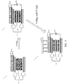
FIG. 3 , the driving voltage is applied between the electrode plate and the second electrode layer, so that the reaction monomer and the liquid crystal molecules are arranged at a pre-tilt angle. Afterwards, the driving voltage is continuously applied, and the electrode plate irradiated with ultraviolet (UV) light, to generate a polymerization reaction of the reaction monomer, deposit the reaction monomer on a surface of the first alignment film and a surface of the second alignment film, and thus fix the liquid crystal molecules at the pre-tilt angle. - In some embodiments, after the step of performing the alignment on the liquid crystal layer, the electrode plate is also removed from the first substrate. Increase in the thickness of the liquid crystal display panel, on whose liquid crystals the alignment is performed in the aforementioned method, is avoided.
- In the embodiment of the present disclosure, as shown in
FIG. 4 , a liquidcrystal alignment system 1 is provided, and includes a liquidcrystal display panel 1000, apower source 2000, and anelectrode plate 3000 being independent from the liquid crystal display panel. - The liquid
crystal display panel 1000 includes afirst substrate 100, a second 200, and aliquid crystal layer 300. Thefirst substrate 100 includes afirst electrode layer 101 and afirst alignment film 102 covering thefirst electrode layer 101. Thesecond substrate 200 is disposed opposite to thefirst substrate 100, and includes asecond electrode layer 201 and asecond alignment film 202 covering thesecond electrode layer 201. Theliquid crystal layer 300 is disposed between thefirst alignment film 102 and thesecond alignment film 202. In some embodiments, the material of thefirst alignment film 102 and thesecond alignment film 202 include polyimides. - The
electrode plate 3000 is disposed on a side of thefirst substrate 100 away from thefirst electrode layer 101. In some embodiments, theelectrode plate 3000 includes aglass substrate 3001 and anelectrode layer 3002 disposed between theglass substrate 3001 and thefirst electrode layer 101. In some embodiments, the material of the electrode layer 402 includes indium tin oxide. - The
power source 2000 is connected to theelectrode plate 3000 and thesecond electrode layer 201. Thepower source 2000 is configured to apply a driving voltage to theelectrode plate 3000 and thesecond electrode layer 201 to align theliquid crystal layer 300. Specifically, thepower source 2000 is connected to theelectrode layer 3002 of theelectrode plate 3000 and thesecond electrode layer 201. Thepower source 2000 is configured to apply the driving voltage to theelectrode layer 3002 of theelectrode plate 3000 and thesecond electrode layer 201. - In some embodiments, the liquid
crystal alignment system 1 further includes alight source 4000, as shown inFIG. 5 . Thelight source 4000 is configured to irradiate theelectrode plate 3000 with ultraviolet light, to generate a polymerization reaction of the reaction monomer in theliquid crystal layer 300, deposit the reaction monomer on a surface of thefirst alignment film 102 and a surface of thesecond alignment film 202, and thus fix the liquid crystal molecules at a pre-tilt angle in theliquid crystal layer 300. - In some embodiments, the liquid
crystal alignment system 1 further includes a removing device, such as a clamp, for removing theelectrode plate 3000 from thefirst substrate 100. - Specifically, as shown in
FIG. 3 , in the liquidcrystal alignment system 1, the alignment process performed on theliquid crystal panel 1000 is as follows: the driving voltage is applied by thepower source 2000 between the electrode plate 402 and thesecond electrode layer 201, so that the reaction monomer and the liquid crystal molecules in theliquid crystal layer 300 are arranged at the pre-tilt angle. Afterwards, the driving voltage is continuously applied by thepower source 2000, and the electrode plate 400 irradiated with ultraviolet (UV) light by thelight resource 4000, to generate a polymerization reaction of the reaction monomer, deposit the reaction monomer on a surface of thefirst alignment film 102 and a surface of thesecond alignment film 202, and thus fix the liquid crystal molecules at the pre-tilt angle. - The number of wires on the liquid crystal display panel is reduced by disposing the electrode plate on the first substrate to perform the alignment on the liquid crystal layer in the method for aligning the liquid crystals and the liquid crystal alignment system in the present disclosure.
- In summary, although the preferable embodiments of the present disclosure have been disclosed above, the embodiments are not intended to limit the present disclosure. A person of ordinary skill in the art, without departing from the spirit and scope of the present disclosure, can make various modifications and variations. Therefore, the scope of the disclosure is defined in the claims.
Claims (20)
- A method for aligning liquid crystals, comprising steps of:providing a first substrate formed with a first electrode layer thereon and a first alignment film covering the first electrode layer, wherein material of the first alignment film includes polyimide;providing a second substrate disposed opposite to the first substrate, and formed with a second electrode layer thereon and a second alignment film covering the second electrode layer, wherein material of the second alignment film includes polyimide;forming a liquid crystal layer between the first alignment film and the second alignment film;providing an electrode plate and disposing the electrode plate on a side of the first substrate away from the first electrode layer;applying a driving voltage between the electrode plate and the second electrode layer to align the liquid crystal layer; andremoving the electrode plate from the first substrate.
- The method for aligning the liquid crystals as claimed in claim 1, wherein the liquid crystal layer includes a reaction monomer and liquid crystal molecules, and the step of applying the driving voltage between the electrode plate and the second electrode layer to align the liquid crystal layer includes steps of:applying the driving voltage between the electrode plate and the second electrode layer, to arrange the reaction monomer and the liquid crystal molecules at a pre-tilt angle;continuously applying the driving voltage, and irradiating the electrode plate with ultraviolet light, to generate a polymerization reaction of the reaction monomer, deposit the reaction monomer on a surface of the first alignment film and a surface of the second alignment film, and thus fix the liquid crystal molecules at the pre-tilt angle.
- The method for aligning the liquid crystals as claimed in claim 1, wherein the electrode plate includes a glass substrate and an electrode layer, and the step of applying the driving voltage between the electrode plate and the second electrode layer includes a step of:
applying the driving voltage between the electrode layer of the electrode plate and the second electrode layer. - The method for aligning the liquid crystals as claimed in claim 3, wherein material of the electrode layer includes indium tin oxide.
- The method for aligning the liquid crystals as claimed in claim 1, wherein the first substrate is a color filter substrate.
- The method for aligning the liquid crystals as claimed in claim 1, wherein the second substrate is an array substrate.
- A method for aligning liquid crystals, comprising steps of:providing a first substrate formed with a first electrode layer thereon and a first alignment film covering the first electrode layer;providing a second substrate disposed opposite to the first substrate, and formed with a second electrode layer thereon and a second alignment film covering the second electrode layer;forming a liquid crystal layer between the first alignment film and the second alignment film;providing an electrode plate and disposing the electrode plate on a side of the first substrate away from the first electrode layer; andapplying a driving voltage between the electrode plate and the second electrode layer to align the liquid crystal layer.
- The method for aligning the liquid crystals as claimed in claim 7, wherein the liquid crystal layer includes a reaction monomer and liquid crystal molecules, and the step of applying the driving voltage between the electrode plate and the second electrode layer to align the liquid crystal layer includes steps of:applying the driving voltage between the electrode plate and the second electrode layer, to arrange the reaction monomer and the liquid crystal molecules at a pre-tilt angle;continuously applying the driving voltage, and irradiating the electrode plate with ultraviolet light, to generate a polymerization reaction of the reaction monomer, deposit the reaction monomer on a surface of the first alignment film and a surface of the second alignment film, and thus fix the liquid crystal molecules at the pre-tilt angle.
- The method for aligning the liquid crystals as claimed in claim 7, wherein the electrode plate includes a glass substrate and an electrode layer, and the step of applying the driving voltage between the electrode plate and the second electrode layer includes a step of:
applying the driving voltage between the electrode layer of the electrode plate and the second electrode layer. - The method for aligning the liquid crystals as claimed in claim 9, wherein material of the electrode layer includes indium tin oxide.
- The method for aligning the liquid crystals as claimed in claim 7, after the step of performing the alignment on the liquid crystal layer, further comprising a step of:
removing the electrode plate from the first substrate. - The method for aligning the liquid crystals as claimed in claim 7, wherein material of the first alignment film and material of the second alignment film include polyimide.
- The method for aligning the liquid crystals as claimed in claim 7, wherein the first substrate is a color filter substrate.
- The method for aligning the liquid crystals as claimed in claim 7, wherein the second substrate is an array substrate.
- A liquid crystal alignment system, comprising
a liquid crystal display panel;
a power source; and
an electrode plate being independent from the liquid crystal display panel;
wherein the liquid crystal display panel includes:a first substrate including a first electrode layer and a first alignment film covering the first electrode layer;a second substrate disposed opposite to the first substrate, and including a second electrode layer and a second alignment film covering the second electrode layer; anda liquid crystal layer disposed between the first alignment film and the second alignment film;wherein the electrode plate is disposed on a side of the first substrate away from the first electrode layer;
wherein the power source is connected to the electrode plate and the second electrode layer, and the power source is configured to apply a driving voltage to the electrode plate and the second electrode layer to align the liquid crystal layer. - The liquid crystal alignment system as claimed in claim 15, wherein the liquid crystal layer includes a reaction monomer and liquid crystal molecules, the liquid crystal alignment system further includes a light source, and
wherein the light source is configured to irradiate the electrode plate with ultraviolet light, to generate a polymerization reaction of the reaction monomer, deposit the reaction monomer on a surface of the first alignment film and a surface of the second alignment film, and thus fix the liquid crystal molecules at the pre-tilt angle. - The liquid crystal alignment system as claimed in claim 15, wherein the electrode plate includes a glass substrate and an electrode layer, the electrode layer is disposed between the glass substrate and the first electrode layer, and
wherein the power source is connected to the electrode layer of the electrode plate and the second electrode layer, and is configured to apply the driving voltage to the electrode plate of the electrode plate and the second electrode layer. - The liquid crystal alignment system as claimed in claim 15, further comprising a removing device configured to remove the electrode plate from the first substrate.
- The liquid crystal alignment system as claimed in claim 15, wherein the first substrate is a color filter substrate.
- The liquid crystal alignment system as claimed in claim 15, wherein the second substrate is an array substrate.
Applications Claiming Priority (2)
| Application Number | Priority Date | Filing Date | Title |
|---|---|---|---|
| CN201710865496.2A CN107703682B (en) | 2017-09-22 | 2017-09-22 | LCD alignment method and LCD alignment system |
| PCT/CN2017/110318 WO2019056528A1 (en) | 2017-09-22 | 2017-11-10 | Liquid crystal alignment method and liquid crystal alignment system |
Publications (3)
| Publication Number | Publication Date |
|---|---|
| EP3686663A1 true EP3686663A1 (en) | 2020-07-29 |
| EP3686663A4 EP3686663A4 (en) | 2021-05-26 |
| EP3686663B1 EP3686663B1 (en) | 2026-07-08 |
Family
ID=61171837
Family Applications (1)
| Application Number | Title | Priority Date | Filing Date |
|---|---|---|---|
| EP17926131.8A Active EP3686663B1 (en) | 2017-09-22 | 2017-11-10 | Liquid crystal alignment method and liquid crystal alignment system |
Country Status (6)
| Country | Link |
|---|---|
| US (1) | US10564481B2 (en) |
| EP (1) | EP3686663B1 (en) |
| JP (1) | JP7072055B2 (en) |
| KR (1) | KR20200052375A (en) |
| CN (1) | CN107703682B (en) |
| WO (1) | WO2019056528A1 (en) |
Families Citing this family (2)
| Publication number | Priority date | Publication date | Assignee | Title |
|---|---|---|---|---|
| CN110196518A (en) * | 2019-06-10 | 2019-09-03 | 成都中电熊猫显示科技有限公司 | Alignment method of liquid crystal panel, liquid crystal panel and display device |
| CN114141787B (en) * | 2021-10-27 | 2025-04-29 | 重庆惠科金渝光电科技有限公司 | Array substrate and preparation method thereof, and display panel |
Family Cites Families (16)
| Publication number | Priority date | Publication date | Assignee | Title |
|---|---|---|---|---|
| JP4849733B2 (en) | 2000-05-11 | 2012-01-11 | 株式会社半導体エネルギー研究所 | Manufacturing method of active matrix type liquid crystal display device |
| JP2003005171A (en) * | 2001-06-19 | 2003-01-08 | Rohm Co Ltd | Liquid crystal display device and manufacturing method thereof |
| JP2003029265A (en) | 2001-07-18 | 2003-01-29 | Optrex Corp | Liquid crystal panel, manufacturing method thereof, and liquid crystal display device |
| JP2008242036A (en) * | 2007-03-27 | 2008-10-09 | Sharp Corp | Liquid crystal display device and manufacturing method thereof |
| KR20100032324A (en) * | 2008-09-17 | 2010-03-25 | 삼성전자주식회사 | Liquid crystal display and manufacturing method of the same |
| CN101872098B (en) * | 2009-04-24 | 2012-08-01 | 上海天马微电子有限公司 | Liquid crystal display panel and method for manufacturing the same |
| JP5538948B2 (en) * | 2010-02-24 | 2014-07-02 | シチズンファインテックミヨタ株式会社 | Manufacturing method of liquid crystal display element |
| CN102681269B (en) * | 2012-05-07 | 2015-01-07 | 深圳市华星光电技术有限公司 | Liquid crystal display device and manufacturing method thereof |
| KR102053290B1 (en) * | 2013-09-09 | 2019-12-09 | 삼성디스플레이 주식회사 | Method for manufacturing liquid crystal device |
| WO2016021862A1 (en) | 2014-08-04 | 2016-02-11 | Lg Innotek Co., Ltd. | Touch window |
| CN105093686B (en) | 2015-02-06 | 2018-01-12 | 深圳市华星光电技术有限公司 | Liquid crystal orienting film preparation method and reaction board |
| CN104977758A (en) * | 2015-07-31 | 2015-10-14 | 深圳市华星光电技术有限公司 | Alignment method suitable for PSVA type liquid crystal display panel |
| CN105629585A (en) * | 2016-01-13 | 2016-06-01 | 深圳市华星光电技术有限公司 | Liquid crystal display panel structure and manufacturing method thereof |
| CN105446019B (en) * | 2016-01-21 | 2019-08-02 | 深圳市华星光电技术有限公司 | A kind of display panel production method and liquid crystal display |
| CN105467636A (en) * | 2016-02-17 | 2016-04-06 | 京东方科技集团股份有限公司 | Light control film, preparation method of light control film and vehicle-mounted display screen |
| CN105629587A (en) * | 2016-03-25 | 2016-06-01 | 京东方科技集团股份有限公司 | Display panel, preparing method of display panel and display device |
-
2017
- 2017-09-22 CN CN201710865496.2A patent/CN107703682B/en active Active
- 2017-11-10 EP EP17926131.8A patent/EP3686663B1/en active Active
- 2017-11-10 JP JP2020516712A patent/JP7072055B2/en active Active
- 2017-11-10 WO PCT/CN2017/110318 patent/WO2019056528A1/en not_active Ceased
- 2017-11-10 US US15/574,896 patent/US10564481B2/en not_active Expired - Fee Related
- 2017-11-10 KR KR1020207011521A patent/KR20200052375A/en not_active Ceased
Also Published As
| Publication number | Publication date |
|---|---|
| CN107703682A (en) | 2018-02-16 |
| JP2020534583A (en) | 2020-11-26 |
| CN107703682B (en) | 2019-11-15 |
| JP7072055B2 (en) | 2022-05-19 |
| KR20200052375A (en) | 2020-05-14 |
| WO2019056528A1 (en) | 2019-03-28 |
| US20190094629A1 (en) | 2019-03-28 |
| US10564481B2 (en) | 2020-02-18 |
| EP3686663B1 (en) | 2026-07-08 |
| EP3686663A4 (en) | 2021-05-26 |
Similar Documents
| Publication | Publication Date | Title |
|---|---|---|
| US9804433B2 (en) | Liquid crystal display panel of improving color washout | |
| JP6317582B2 (en) | Liquid crystal display and manufacturing method thereof | |
| US6778229B2 (en) | Liquid crystal display device and method of fabricating the same | |
| US20120129285A1 (en) | Methods for manufacturing display panel and display apparatus | |
| KR100259440B1 (en) | Active matrix type lcd apparatus and formation method and orientation verification method of orientation film thereof | |
| US9239498B2 (en) | Liquid crystal display device and manufacturing method thereof | |
| CN103792710A (en) | Method of manufacturing liquid crystal display | |
| US9041880B2 (en) | Optical compensated bending mode liquid crystal display panel and method for manufacturing the same | |
| US20100259469A1 (en) | Liquid crystal display panel and liquid crystal display device | |
| CN111413827B (en) | Liquid crystal display panel and pretilt angle forming method | |
| US20180210293A1 (en) | Liquid crystal panels, liquid crystal alignment methods thereof and liquid crystal displays | |
| US20130314656A1 (en) | Liquid Crystal Panel And Method Of Liquid Crystal Alignment | |
| US10564481B2 (en) | Method for aligning liquid crystals and liquid crystal alignment system | |
| KR102073957B1 (en) | Liquid crystal display panel and mathod for fabricating the same | |
| US9904117B2 (en) | Display panel manufacturing method and liquid crystal display device | |
| US20130010220A1 (en) | Liquid crystal display panel and manufacturing method thereof | |
| US10663801B2 (en) | Alignment agent, manufacturing method of alignment film, display panel and display device | |
| KR100244537B1 (en) | A liquid crystal display device | |
| US20140078439A1 (en) | Dual-TFT-Substrate Blue-Phase Liquid Crystal Display Panel | |
| US9170460B2 (en) | In-plane-switching mode liquid crystal panel, manufacturing process and display device thereof | |
| US10509265B2 (en) | Photo-alignment apparatus and photo-alignment method | |
| WO2019153474A1 (en) | Display component and manufacturing method therefor | |
| JP2017181816A (en) | Display device, liquid crystal display device, and manufacturing method for display device | |
| KR102450012B1 (en) | Method and apparatus for controlling contact angle through plasma and UVO treatment | |
| CN105093694B (en) | The alignment method of FFS type liquid crystal panels |
Legal Events
| Date | Code | Title | Description |
|---|---|---|---|
| STAA | Information on the status of an ep patent application or granted ep patent |
Free format text: STATUS: THE INTERNATIONAL PUBLICATION HAS BEEN MADE |
|
| PUAI | Public reference made under article 153(3) epc to a published international application that has entered the european phase |
Free format text: ORIGINAL CODE: 0009012 |
|
| STAA | Information on the status of an ep patent application or granted ep patent |
Free format text: STATUS: REQUEST FOR EXAMINATION WAS MADE |
|
| 17P | Request for examination filed |
Effective date: 20200417 |
|
| AK | Designated contracting states |
Kind code of ref document: A1 Designated state(s): AL AT BE BG CH CY CZ DE DK EE ES FI FR GB GR HR HU IE IS IT LI LT LU LV MC MK MT NL NO PL PT RO RS SE SI SK SM TR |
|
| AX | Request for extension of the european patent |
Extension state: BA ME |
|
| DAV | Request for validation of the european patent (deleted) | ||
| DAX | Request for extension of the european patent (deleted) | ||
| A4 | Supplementary search report drawn up and despatched |
Effective date: 20210426 |
|
| RIC1 | Information provided on ipc code assigned before grant |
Ipc: G02F 1/1337 20060101AFI20210420BHEP |
|
| STAA | Information on the status of an ep patent application or granted ep patent |
Free format text: STATUS: EXAMINATION IS IN PROGRESS |
|
| 17Q | First examination report despatched |
Effective date: 20230414 |
|
| GRAP | Despatch of communication of intention to grant a patent |
Free format text: ORIGINAL CODE: EPIDOSNIGR1 |
|
| STAA | Information on the status of an ep patent application or granted ep patent |
Free format text: STATUS: GRANT OF PATENT IS INTENDED |
|
| RIC1 | Information provided on ipc code assigned before grant |
Ipc: G02F 1/1337 20060101AFI20260204BHEP Ipc: G02F 1/13 20060101ALI20260204BHEP |
|
| INTG | Intention to grant announced |
Effective date: 20260225 |
|
| GRAS | Grant fee paid |
Free format text: ORIGINAL CODE: EPIDOSNIGR3 |
|
| GRAA | (expected) grant |
Free format text: ORIGINAL CODE: 0009210 |
|
| STAA | Information on the status of an ep patent application or granted ep patent |
Free format text: STATUS: THE PATENT HAS BEEN GRANTED |
|
| P01 | Opt-out of the competence of the unified patent court (upc) registered |
Free format text: CASE NUMBER: UPC_APP_0016312_3686663/2026 Effective date: 20260521 |
|
| AK | Designated contracting states |
Kind code of ref document: B1 Designated state(s): AL AT BE BG CH CY CZ DE DK EE ES FI FR GB GR HR HU IE IS IT LI LT LU LV MC MK MT NL NO PL PT RO RS SE SI SK SM TR |
|
| REG | Reference to a national code |
Ref country code: CH Ref legal event code: F10 Free format text: ST27 STATUS EVENT CODE: U-0-0-F10-F00 (AS PROVIDED BY THE NATIONAL OFFICE) Effective date: 20260708 Ref country code: GB Ref legal event code: FG4D |
|
| REG | Reference to a national code |
Ref country code: IE Ref legal event code: FG4D |
|
| REG | Reference to a national code |
Ref country code: DE Ref legal event code: R096 Ref document number: 602017095920 Country of ref document: DE |