EP3686316A1 - Method for producing layer and apparatus for producing same, metal oxide transistor and method for producing same - Google Patents
Method for producing layer and apparatus for producing same, metal oxide transistor and method for producing same Download PDFInfo
- Publication number
- EP3686316A1 EP3686316A1 EP18810875.7A EP18810875A EP3686316A1 EP 3686316 A1 EP3686316 A1 EP 3686316A1 EP 18810875 A EP18810875 A EP 18810875A EP 3686316 A1 EP3686316 A1 EP 3686316A1
- Authority
- EP
- European Patent Office
- Prior art keywords
- chamber
- dosing
- metal oxide
- source gas
- layer
- Prior art date
- Legal status (The legal status is an assumption and is not a legal conclusion. Google has not performed a legal analysis and makes no representation as to the accuracy of the status listed.)
- Pending
Links
Images







Classifications
-
- C—CHEMISTRY; METALLURGY
- C23—COATING METALLIC MATERIAL; COATING MATERIAL WITH METALLIC MATERIAL; CHEMICAL SURFACE TREATMENT; DIFFUSION TREATMENT OF METALLIC MATERIAL; COATING BY VACUUM EVAPORATION, BY SPUTTERING, BY ION IMPLANTATION OR BY CHEMICAL VAPOUR DEPOSITION, IN GENERAL; INHIBITING CORROSION OF METALLIC MATERIAL OR INCRUSTATION IN GENERAL
- C23C—COATING METALLIC MATERIAL; COATING MATERIAL WITH METALLIC MATERIAL; SURFACE TREATMENT OF METALLIC MATERIAL BY DIFFUSION INTO THE SURFACE, BY CHEMICAL CONVERSION OR SUBSTITUTION; COATING BY VACUUM EVAPORATION, BY SPUTTERING, BY ION IMPLANTATION OR BY CHEMICAL VAPOUR DEPOSITION, IN GENERAL
- C23C16/00—Chemical coating by decomposition of gaseous compounds, without leaving reaction products of surface material in the coating, i.e. chemical vapour deposition [CVD] processes
- C23C16/22—Chemical coating by decomposition of gaseous compounds, without leaving reaction products of surface material in the coating, i.e. chemical vapour deposition [CVD] processes characterised by the deposition of inorganic material, other than metallic material
- C23C16/30—Deposition of compounds, mixtures or solid solutions, e.g. borides, carbides, nitrides
- C23C16/40—Oxides
- C23C16/407—Oxides of zinc, germanium, cadmium, indium, tin, thallium or bismuth
-
- C—CHEMISTRY; METALLURGY
- C23—COATING METALLIC MATERIAL; COATING MATERIAL WITH METALLIC MATERIAL; CHEMICAL SURFACE TREATMENT; DIFFUSION TREATMENT OF METALLIC MATERIAL; COATING BY VACUUM EVAPORATION, BY SPUTTERING, BY ION IMPLANTATION OR BY CHEMICAL VAPOUR DEPOSITION, IN GENERAL; INHIBITING CORROSION OF METALLIC MATERIAL OR INCRUSTATION IN GENERAL
- C23C—COATING METALLIC MATERIAL; COATING MATERIAL WITH METALLIC MATERIAL; SURFACE TREATMENT OF METALLIC MATERIAL BY DIFFUSION INTO THE SURFACE, BY CHEMICAL CONVERSION OR SUBSTITUTION; COATING BY VACUUM EVAPORATION, BY SPUTTERING, BY ION IMPLANTATION OR BY CHEMICAL VAPOUR DEPOSITION, IN GENERAL
- C23C16/00—Chemical coating by decomposition of gaseous compounds, without leaving reaction products of surface material in the coating, i.e. chemical vapour deposition [CVD] processes
- C23C16/44—Chemical coating by decomposition of gaseous compounds, without leaving reaction products of surface material in the coating, i.e. chemical vapour deposition [CVD] processes characterised by the method of coating
- C23C16/448—Chemical coating by decomposition of gaseous compounds, without leaving reaction products of surface material in the coating, i.e. chemical vapour deposition [CVD] processes characterised by the method of coating characterised by the method used for generating reactive gas streams, e.g. by evaporation or sublimation of precursor materials
-
- H—ELECTRICITY
- H10—SEMICONDUCTOR DEVICES; ELECTRIC SOLID-STATE DEVICES NOT OTHERWISE PROVIDED FOR
- H10P—GENERIC PROCESSES OR APPARATUS FOR THE MANUFACTURE OR TREATMENT OF DEVICES COVERED BY CLASS H10
- H10P14/00—Formation of materials, e.g. in the shape of layers or pillars
- H10P14/20—Formation of materials, e.g. in the shape of layers or pillars of semiconductor materials
- H10P14/24—Formation of materials, e.g. in the shape of layers or pillars of semiconductor materials using chemical vapour deposition [CVD]
-
- C—CHEMISTRY; METALLURGY
- C23—COATING METALLIC MATERIAL; COATING MATERIAL WITH METALLIC MATERIAL; CHEMICAL SURFACE TREATMENT; DIFFUSION TREATMENT OF METALLIC MATERIAL; COATING BY VACUUM EVAPORATION, BY SPUTTERING, BY ION IMPLANTATION OR BY CHEMICAL VAPOUR DEPOSITION, IN GENERAL; INHIBITING CORROSION OF METALLIC MATERIAL OR INCRUSTATION IN GENERAL
- C23C—COATING METALLIC MATERIAL; COATING MATERIAL WITH METALLIC MATERIAL; SURFACE TREATMENT OF METALLIC MATERIAL BY DIFFUSION INTO THE SURFACE, BY CHEMICAL CONVERSION OR SUBSTITUTION; COATING BY VACUUM EVAPORATION, BY SPUTTERING, BY ION IMPLANTATION OR BY CHEMICAL VAPOUR DEPOSITION, IN GENERAL
- C23C16/00—Chemical coating by decomposition of gaseous compounds, without leaving reaction products of surface material in the coating, i.e. chemical vapour deposition [CVD] processes
- C23C16/44—Chemical coating by decomposition of gaseous compounds, without leaving reaction products of surface material in the coating, i.e. chemical vapour deposition [CVD] processes characterised by the method of coating
- C23C16/4401—Means for minimising impurities, e.g. dust, moisture or residual gas, in the reaction chamber
- C23C16/4408—Means for minimising impurities, e.g. dust, moisture or residual gas, in the reaction chamber by purging residual gases from the reaction chamber or gas lines
-
- C—CHEMISTRY; METALLURGY
- C23—COATING METALLIC MATERIAL; COATING MATERIAL WITH METALLIC MATERIAL; CHEMICAL SURFACE TREATMENT; DIFFUSION TREATMENT OF METALLIC MATERIAL; COATING BY VACUUM EVAPORATION, BY SPUTTERING, BY ION IMPLANTATION OR BY CHEMICAL VAPOUR DEPOSITION, IN GENERAL; INHIBITING CORROSION OF METALLIC MATERIAL OR INCRUSTATION IN GENERAL
- C23C—COATING METALLIC MATERIAL; COATING MATERIAL WITH METALLIC MATERIAL; SURFACE TREATMENT OF METALLIC MATERIAL BY DIFFUSION INTO THE SURFACE, BY CHEMICAL CONVERSION OR SUBSTITUTION; COATING BY VACUUM EVAPORATION, BY SPUTTERING, BY ION IMPLANTATION OR BY CHEMICAL VAPOUR DEPOSITION, IN GENERAL
- C23C16/00—Chemical coating by decomposition of gaseous compounds, without leaving reaction products of surface material in the coating, i.e. chemical vapour deposition [CVD] processes
- C23C16/44—Chemical coating by decomposition of gaseous compounds, without leaving reaction products of surface material in the coating, i.e. chemical vapour deposition [CVD] processes characterised by the method of coating
- C23C16/455—Chemical coating by decomposition of gaseous compounds, without leaving reaction products of surface material in the coating, i.e. chemical vapour deposition [CVD] processes characterised by the method of coating characterised by the method used for introducing gases into reaction chamber or for modifying gas flows in reaction chamber
-
- C—CHEMISTRY; METALLURGY
- C23—COATING METALLIC MATERIAL; COATING MATERIAL WITH METALLIC MATERIAL; CHEMICAL SURFACE TREATMENT; DIFFUSION TREATMENT OF METALLIC MATERIAL; COATING BY VACUUM EVAPORATION, BY SPUTTERING, BY ION IMPLANTATION OR BY CHEMICAL VAPOUR DEPOSITION, IN GENERAL; INHIBITING CORROSION OF METALLIC MATERIAL OR INCRUSTATION IN GENERAL
- C23C—COATING METALLIC MATERIAL; COATING MATERIAL WITH METALLIC MATERIAL; SURFACE TREATMENT OF METALLIC MATERIAL BY DIFFUSION INTO THE SURFACE, BY CHEMICAL CONVERSION OR SUBSTITUTION; COATING BY VACUUM EVAPORATION, BY SPUTTERING, BY ION IMPLANTATION OR BY CHEMICAL VAPOUR DEPOSITION, IN GENERAL
- C23C16/00—Chemical coating by decomposition of gaseous compounds, without leaving reaction products of surface material in the coating, i.e. chemical vapour deposition [CVD] processes
- C23C16/44—Chemical coating by decomposition of gaseous compounds, without leaving reaction products of surface material in the coating, i.e. chemical vapour deposition [CVD] processes characterised by the method of coating
- C23C16/455—Chemical coating by decomposition of gaseous compounds, without leaving reaction products of surface material in the coating, i.e. chemical vapour deposition [CVD] processes characterised by the method of coating characterised by the method used for introducing gases into reaction chamber or for modifying gas flows in reaction chamber
- C23C16/45523—Pulsed gas flow or change of composition over time
-
- C—CHEMISTRY; METALLURGY
- C23—COATING METALLIC MATERIAL; COATING MATERIAL WITH METALLIC MATERIAL; CHEMICAL SURFACE TREATMENT; DIFFUSION TREATMENT OF METALLIC MATERIAL; COATING BY VACUUM EVAPORATION, BY SPUTTERING, BY ION IMPLANTATION OR BY CHEMICAL VAPOUR DEPOSITION, IN GENERAL; INHIBITING CORROSION OF METALLIC MATERIAL OR INCRUSTATION IN GENERAL
- C23C—COATING METALLIC MATERIAL; COATING MATERIAL WITH METALLIC MATERIAL; SURFACE TREATMENT OF METALLIC MATERIAL BY DIFFUSION INTO THE SURFACE, BY CHEMICAL CONVERSION OR SUBSTITUTION; COATING BY VACUUM EVAPORATION, BY SPUTTERING, BY ION IMPLANTATION OR BY CHEMICAL VAPOUR DEPOSITION, IN GENERAL
- C23C16/00—Chemical coating by decomposition of gaseous compounds, without leaving reaction products of surface material in the coating, i.e. chemical vapour deposition [CVD] processes
- C23C16/44—Chemical coating by decomposition of gaseous compounds, without leaving reaction products of surface material in the coating, i.e. chemical vapour deposition [CVD] processes characterised by the method of coating
- C23C16/455—Chemical coating by decomposition of gaseous compounds, without leaving reaction products of surface material in the coating, i.e. chemical vapour deposition [CVD] processes characterised by the method of coating characterised by the method used for introducing gases into reaction chamber or for modifying gas flows in reaction chamber
- C23C16/45523—Pulsed gas flow or change of composition over time
- C23C16/45525—Atomic layer deposition [ALD]
- C23C16/45527—Atomic layer deposition [ALD] characterized by the ALD cycle, e.g. different flows or temperatures during half-reactions, unusual pulsing sequence, use of precursor mixtures or auxiliary reactants or activations
-
- C—CHEMISTRY; METALLURGY
- C23—COATING METALLIC MATERIAL; COATING MATERIAL WITH METALLIC MATERIAL; CHEMICAL SURFACE TREATMENT; DIFFUSION TREATMENT OF METALLIC MATERIAL; COATING BY VACUUM EVAPORATION, BY SPUTTERING, BY ION IMPLANTATION OR BY CHEMICAL VAPOUR DEPOSITION, IN GENERAL; INHIBITING CORROSION OF METALLIC MATERIAL OR INCRUSTATION IN GENERAL
- C23C—COATING METALLIC MATERIAL; COATING MATERIAL WITH METALLIC MATERIAL; SURFACE TREATMENT OF METALLIC MATERIAL BY DIFFUSION INTO THE SURFACE, BY CHEMICAL CONVERSION OR SUBSTITUTION; COATING BY VACUUM EVAPORATION, BY SPUTTERING, BY ION IMPLANTATION OR BY CHEMICAL VAPOUR DEPOSITION, IN GENERAL
- C23C16/00—Chemical coating by decomposition of gaseous compounds, without leaving reaction products of surface material in the coating, i.e. chemical vapour deposition [CVD] processes
- C23C16/44—Chemical coating by decomposition of gaseous compounds, without leaving reaction products of surface material in the coating, i.e. chemical vapour deposition [CVD] processes characterised by the method of coating
- C23C16/455—Chemical coating by decomposition of gaseous compounds, without leaving reaction products of surface material in the coating, i.e. chemical vapour deposition [CVD] processes characterised by the method of coating characterised by the method used for introducing gases into reaction chamber or for modifying gas flows in reaction chamber
- C23C16/45523—Pulsed gas flow or change of composition over time
- C23C16/45525—Atomic layer deposition [ALD]
- C23C16/45553—Atomic layer deposition [ALD] characterized by the use of precursors specially adapted for ALD
-
- C—CHEMISTRY; METALLURGY
- C23—COATING METALLIC MATERIAL; COATING MATERIAL WITH METALLIC MATERIAL; CHEMICAL SURFACE TREATMENT; DIFFUSION TREATMENT OF METALLIC MATERIAL; COATING BY VACUUM EVAPORATION, BY SPUTTERING, BY ION IMPLANTATION OR BY CHEMICAL VAPOUR DEPOSITION, IN GENERAL; INHIBITING CORROSION OF METALLIC MATERIAL OR INCRUSTATION IN GENERAL
- C23C—COATING METALLIC MATERIAL; COATING MATERIAL WITH METALLIC MATERIAL; SURFACE TREATMENT OF METALLIC MATERIAL BY DIFFUSION INTO THE SURFACE, BY CHEMICAL CONVERSION OR SUBSTITUTION; COATING BY VACUUM EVAPORATION, BY SPUTTERING, BY ION IMPLANTATION OR BY CHEMICAL VAPOUR DEPOSITION, IN GENERAL
- C23C16/00—Chemical coating by decomposition of gaseous compounds, without leaving reaction products of surface material in the coating, i.e. chemical vapour deposition [CVD] processes
- C23C16/44—Chemical coating by decomposition of gaseous compounds, without leaving reaction products of surface material in the coating, i.e. chemical vapour deposition [CVD] processes characterised by the method of coating
- C23C16/455—Chemical coating by decomposition of gaseous compounds, without leaving reaction products of surface material in the coating, i.e. chemical vapour deposition [CVD] processes characterised by the method of coating characterised by the method used for introducing gases into reaction chamber or for modifying gas flows in reaction chamber
- C23C16/45557—Pulsed pressure or control pressure
-
- C—CHEMISTRY; METALLURGY
- C23—COATING METALLIC MATERIAL; COATING MATERIAL WITH METALLIC MATERIAL; CHEMICAL SURFACE TREATMENT; DIFFUSION TREATMENT OF METALLIC MATERIAL; COATING BY VACUUM EVAPORATION, BY SPUTTERING, BY ION IMPLANTATION OR BY CHEMICAL VAPOUR DEPOSITION, IN GENERAL; INHIBITING CORROSION OF METALLIC MATERIAL OR INCRUSTATION IN GENERAL
- C23C—COATING METALLIC MATERIAL; COATING MATERIAL WITH METALLIC MATERIAL; SURFACE TREATMENT OF METALLIC MATERIAL BY DIFFUSION INTO THE SURFACE, BY CHEMICAL CONVERSION OR SUBSTITUTION; COATING BY VACUUM EVAPORATION, BY SPUTTERING, BY ION IMPLANTATION OR BY CHEMICAL VAPOUR DEPOSITION, IN GENERAL
- C23C16/00—Chemical coating by decomposition of gaseous compounds, without leaving reaction products of surface material in the coating, i.e. chemical vapour deposition [CVD] processes
- C23C16/44—Chemical coating by decomposition of gaseous compounds, without leaving reaction products of surface material in the coating, i.e. chemical vapour deposition [CVD] processes characterised by the method of coating
- C23C16/52—Controlling or regulating the coating process
-
- H—ELECTRICITY
- H10—SEMICONDUCTOR DEVICES; ELECTRIC SOLID-STATE DEVICES NOT OTHERWISE PROVIDED FOR
- H10P—GENERIC PROCESSES OR APPARATUS FOR THE MANUFACTURE OR TREATMENT OF DEVICES COVERED BY CLASS H10
- H10P14/00—Formation of materials, e.g. in the shape of layers or pillars
- H10P14/20—Formation of materials, e.g. in the shape of layers or pillars of semiconductor materials
- H10P14/34—Deposited materials, e.g. layers
- H10P14/3402—Deposited materials, e.g. layers characterised by the chemical composition
- H10P14/3424—Deposited materials, e.g. layers characterised by the chemical composition being Group IIB-VIA materials
- H10P14/3426—Oxides
-
- H—ELECTRICITY
- H10—SEMICONDUCTOR DEVICES; ELECTRIC SOLID-STATE DEVICES NOT OTHERWISE PROVIDED FOR
- H10P—GENERIC PROCESSES OR APPARATUS FOR THE MANUFACTURE OR TREATMENT OF DEVICES COVERED BY CLASS H10
- H10P14/00—Formation of materials, e.g. in the shape of layers or pillars
- H10P14/60—Formation of materials, e.g. in the shape of layers or pillars of insulating materials
- H10P14/63—Formation of materials, e.g. in the shape of layers or pillars of insulating materials characterised by the formation processes
- H10P14/6326—Deposition processes
-
- H—ELECTRICITY
- H10—SEMICONDUCTOR DEVICES; ELECTRIC SOLID-STATE DEVICES NOT OTHERWISE PROVIDED FOR
- H10D—INORGANIC ELECTRIC SEMICONDUCTOR DEVICES
- H10D30/00—Field-effect transistors [FET]
- H10D30/60—Insulated-gate field-effect transistors [IGFET]
- H10D30/67—Thin-film transistors [TFT]
- H10D30/674—Thin-film transistors [TFT] characterised by the active materials
- H10D30/6755—Oxide semiconductors, e.g. zinc oxide, copper aluminium oxide or cadmium stannate
-
- H—ELECTRICITY
- H10—SEMICONDUCTOR DEVICES; ELECTRIC SOLID-STATE DEVICES NOT OTHERWISE PROVIDED FOR
- H10D—INORGANIC ELECTRIC SEMICONDUCTOR DEVICES
- H10D99/00—Subject matter not provided for in other groups of this subclass
-
- H—ELECTRICITY
- H10—SEMICONDUCTOR DEVICES; ELECTRIC SOLID-STATE DEVICES NOT OTHERWISE PROVIDED FOR
- H10P—GENERIC PROCESSES OR APPARATUS FOR THE MANUFACTURE OR TREATMENT OF DEVICES COVERED BY CLASS H10
- H10P14/00—Formation of materials, e.g. in the shape of layers or pillars
- H10P14/20—Formation of materials, e.g. in the shape of layers or pillars of semiconductor materials
- H10P14/32—Formation of materials, e.g. in the shape of layers or pillars of semiconductor materials characterised by intermediate layers between substrates and deposited layers
- H10P14/3202—Materials thereof
- H10P14/3238—Materials thereof being insulating materials
Definitions
- the present invention relates to a method and an apparatus for forming a layer, a metal oxide transistor and a fabrication method thereof.
- Metal oxides are currently widely used in various electronic semiconductor devices. They are typically used as active layers or dielectric layers for devices, and various studies on processes for depositing them have also been conducted.
- Another object of the present invention is to provide a method and an apparatus for forming a good-quality layer.
- Still another object of the present invention is to provide a method and an apparatus for forming a layer, which can deposit a layer through a low-temperature process.
- Still another object of the present invention is to provide a method and an apparatus for forming a layer, which can easily control the layer thickness.
- Still another object of the present invention is to provide a method and an apparatus for forming a layer, which can deposit a layer at high rate.
- Still another object of the present invention is to provide a method and an apparatus for forming a layer having an excellent surface morphology.
- Still another object of the present invention is to provide a metal oxide transistor having an active layer including a metal oxide layer, and a method for fabricating the same.
- Still another object of the present invention is to provide a metal oxide transistor having high mobility, and a method for fabricating the same.
- Still another object of the present invention is to provide a metal oxide transistor having high on/off ratio, and a method for fabricating the same.
- a layer forming method may comprise: a source gas dosing/pressurizing step of dosing a source gas into a chamber having a substrate loaded therein in a state in which the outlet of the chamber is closed, thereby increasing the pressure in the chamber and adsorbing the source gas onto the substrate; a first main purging step of purging the chamber, after the source gas dosing/pressurizing step; a reactive gas dosing step of dosing a reactive gas into the chamber, after the first main purging step; and a second main purging step of purging the chamber, after the reactive gas dosing step.
- the source gas dosing/pressurizing step may further comprise the steps of: increasing the pressure in the chamber to a predetermined pressure by dosing the source gas; and maintaining the predetermined pressure by closing the inlet of the chamber.
- the source gas dosing/pressurizing step may comprise at least two sub-dosing/pressurizing steps and a sub-purging step between the at least two sub-dosing/pressurizing steps.
- the source gas dosing/pressurizing step may further comprise, between the sub-dosing/pressurizing step and the sub-purging step, a step of maintaining the chamber pressure that has been increased by the sub-dosing/pressurizing step.
- the reactive gas dosing step may further comprise the steps of: increasing the pressure in the chamber to a predetermined pressure by dosing the reactive gas; and maintaining the predetermined pressure by closing the inlet of the chamber.
- the reactive gas dosing step may comprise at least two sub-dosing/pressurizing steps and a sub-purging step between the at least two sub-dosing/pressurizing steps.
- the reactive gas dosing step may further comprise, between the sub-dosing/pressurizing step and the sub-purging step, a step of maintaining the chamber pressure that has been increased by the sub-dosing/pressurizing step.
- the source gas may comprise a metal precursor for forming a metal oxide layer by deposition.
- the metal oxide layer formed by the source gas dosing/pressurizing step, the first main purging step, the reactive gas dosing step and the second purging step, may have a surface roughness (RMS) lower than 4.4 ⁇ .
- RMS surface roughness
- the metal oxide layer formed by the source gas dosing/pressurizing step, the first main purging step, the reactive gas dosing step and the second purging step, may comprise a plurality of crystalline regions, and an amorphous region surrounding the crystalline regions.
- each of the crystalline regions may have a nanometer size.
- a layer forming apparatus may comprise: an inlet configured to supply a source gas, an inert gas and a reactive gas; a chamber configured to communicate with the inlet and accommodate a substrate; an outlet configured to discharge the gases supplied into the chamber; and a control unit configured to close the outlet when the source gas is supplied into the chamber, thereby increasing the pressure in the chamber and adsorbing the source gas onto the substrate.
- control unit may be configured to close the inlet of the chamber when the pressure in the chamber reaches a predetermine pressure, and to maintain the closed state for a predetermined time.
- control unit may be configured to provide a pressure for at least two sub-dosing/pressurizing steps and a pressure for a sub-purging step between the at least two sub-dosing/pressurizing steps.
- the source gas may comprise a metal oxide precursor for metal oxide deposition.
- a metal oxide transistor may comprise: a gate electrode; a gate insulating layer formed on one side of the gate electrode; an active layer formed on one side of the gate insulating layer and including a metal oxide layer; and source and drain electrodes provided on one side of the active layer.
- the thickness of the metal oxide layer may be greater than 1.5 nm.
- the thickness of the metal oxide layer may be greater than 1.5 nm and not greater than 7 nm.
- the thickness of the metal oxide layer may be greater than 1.5 nm and smaller than 5.0 nm.
- the surface roughness (RMS) of the metal oxide layer may be lower than 4.4 ⁇ .
- a method of fabricating a metal oxide transistor may comprise the steps of: preparing a substrate; and forming an active layer including a metal oxide layer on one side of the substrate, wherein the step of forming the active layer may comprise: a source gas dosing/pressurizing step of dosing a source gas for metal oxide deposition into a chamber having the substrate loaded therein in a state in which the outlet of the chamber is closed, thereby increasing the pressure in the chamber and adsorbing the source gas onto the substrate in the closed chamber; a first main purging step of purging the chamber, after the source gas dosing/pressurizing step; a reactive gas dosing step of dosing a reactive gas into the chamber, thereby depositing a metal oxide layer onto the substrate, after the first main purging step; and a second main purging step of purging the chamber, after the reactive gas dosing step.
- the source gas dosing/pressurizing step, the first main purging step, the reactive gas dosing step and the second main purging step may constitute a unit process, and the electrical properties of the active layer is variable depending on the number of repetitions of the unit process.
- the number of repetitions of the unit process may be greater than 7 and not greater than 35 when the metal oxide layer comprises zinc oxide.
- the source gas dosing/pressurizing step may comprise at least two sub-dosing/pressurizing steps and a sub-purging step between the at least two sub-dosing/pressurizing steps.
- the magnitude of a pressure for each of the at least two sub-dosing/pressurizing steps may increase depending on the number of repetition of the sub-dosing/pressurizing step.
- the source gas dosing/pressurizing step may comprise at least two sub-dosing/pressurizing steps and a sub-purging step between the at least two sub-dosing/pressurizing steps;
- the reactive gas dosing step may further comprise at least two sub-dosing/pressurizing steps and a sub-purging step between the at least two sub-dosing/pressurizing steps; and the time of the sub-purging step of the source gas dosing/pressurizing step may be shorter than that of the sub-purging step of the reactive gas dosing step.
- the source gas may comprise diethyl zinc (DEZ), and the reactive gas may comprise H 2 O.
- DEZ diethyl zinc
- the reactive gas may comprise H 2 O.
- the source gas dosing/pressurizing step, the first main purging step, the reactive gas dosing step and the second main purging step may constitute a unit process, and the unit process may be repeated in a predetermined number.
- the predetermined number may be greater than 7.
- the source gas dosing/pressurizing step may further comprise, after increasing the pressure in the chamber by dosing the source gas, an exposure step of maintaining the increased pressure for a predetermined time.
- a method and apparatus of forming a layer according to one embodiment of the present invention may provide a good-quality layer while depositing the layer in a simple and easy manner.
- a method and apparatus of forming a layer according to one embodiment of the present invention can deposit a layer at low temperature.
- a method and apparatus of forming a layer according to one embodiment of the present invention can easily control the layer thickness.
- a method and apparatus of forming a layer according to one embodiment of the present invention can provide a good-quality layer at high deposition rate.
- a method and apparatus of forming a layer according to one embodiment of the present invention may provide a layer having excellent surface morphology.
- a metal oxide transistor and a fabrication method thereof according to an embodiment of the present invention can exhibit excellent FET characteristics.
- a metal oxide transistor and a fabrication method thereof according to an embodiment of the present invention can exhibit FET characteristics even when a metal oxide layer therein has a very thin thickness.
- any element when any element is referred to as being "on" other element, it means that the element may be formed directly on the other element, or that a third element may be interposed therebetween.
- the thicknesses of layers and regions may have been exaggerated in order to clearly illustrate features of the embodiments.
- connecting includes connecting a plurality of elements both directly and indirectly.
- FIG. 1 illustrates a method of forming a layer according to one embodiment of the present invention
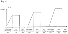
- FIGS. 2 and 3 illustrate step S110 according to one embodiment of the present invention.
- a method of forming a layer by pressure-assisted deposition may comprise at least one of a source gas dosing/pressurizing step (S110), a first main purging step (S120), a reactive gas dosing step (S130), and a second main purging step (S140).
- S110 source gas dosing/pressurizing step
- S120 first main purging step
- S130 reactive gas dosing step
- S140 second main purging step
- a source gas may be prepared.
- the kind of source gas to be prepared may vary depending on the type of layer to be deposited.
- a metal oxide layer a metal precursor source gas corresponding thereto may be prepared.
- the source gas may comprise DEZ (diethyl zinc).
- the source gas may be dosed into a chamber in a state in which the chamber outlet is closed. Accordingly, as the source gas is dosed into the chamber, the pressure in the chamber can increase. In other words, the pressure in the chamber is increased by dosing of the source gas, and hence the source gas may be adsorbed onto a substrate in a pressurized atmosphere.
- step S110 may be higher than 0.03 Torr, preferably, 0.1 Torr or higher, and more preferably 0.3 Torr or higher.
- step S110 may be performed at a temperature of 20°C to 250°C.
- inert gas may be used.
- the inert gas may be, for example, argon (Ar) or nitrogen (N 2 ) gas.
- Ar argon
- N 2 nitrogen
- a reactive gas may react with the source gas to form the layer to be deposited.
- the reactive gas may comprise H 2 O.
- the second main purging step (S140) may further be performed. This can remove an excess of the gas that has not been adsorbed onto the substrate surface.
- Step S110 to step S140 according to one embodiment of the present invention have been described above. Hereinafter, dosing/pressurizing of step S110 will be described in detail.
- the source gas dosing/pressurizing step may be performed in a pressurized atmosphere.
- the source gas dosing/pressurizing step may be performed in a high-pressure atmosphere, and may be abbreviated as "pressurizing step”.
- step S110 the source gas dosing/pressurizing step (step S110) will be described in detail for the sake of brevity, it should be understood that dosing/pressurizing may also be performed in the reactive gas dosing step (step S130).
- the dosing/pressurizing step may be performed in a state in which a chamber having a substrate loaded therein is closed.
- the discharge valve of a chamber is closed, and in this state, a metal precursor source gas may be dosed into the chamber (sub-dosing/pressurizing step), thereby inducing high pressure in the chamber, and the induced high pressure may be maintained (sub-exposure step).
- the metal precursor source gas may be adsorbed onto the substrate surface in a high-pressure atmosphere.
- the dosing/pressurizing step may comprise at least one of a sub-dosing/pressurizing step, a sub-exposure step and a sub-purging step.
- the sub-dosing/pressurizing step may be defined as a step of dosing the source gas into the chamber in a state in which the outlet of the chamber is closed, thereby causing the pressure in the chamber to reach a predetermined pressure.
- the sub-exposure step is a step of maintaining the predetermined pressure provided by the sub-dosing/pressurizing step. To this end, the inlet and outlet of the chamber may all be closed. Namely, the chamber may be closed.
- the sub-purging step may be performed after the sub-exposure step to remove an excess of the source gas dosed.
- the pressure in the sub-exposure step may be maintained at a constant level, even when the number of the sub-exposure steps increases. Unlike this, as shown in FIG. 3 , the pressure in the sub-exposure step may increase as the number of the sub-exposure steps increases.
- step S110 may be performed at a temperature of 80°C to 250°C.
- sub-steps of step S110 may be performed at the same temperature.
- these sub-steps may be performed at low temperature.
- the term "low temperature” refers to a temperature of 250°C or below, preferably 80°C to 250°C.
- the layer forming method according to one embodiment of the present invention has been described above with reference to FIGS. 1 to 3 .
- the performance characteristics of a layer formed according to one embodiment of the present invention will be described.
- FIG. 4 shows process conditions according to one embodiment of the present invention
- FIGS. 5 and 6 show the results of measuring layer growth rate in each of a conventional art and one embodiment of the present invention
- FIGS. 7 and 8 show the results of measuring the surface roughness of each of a layer formed according to a conventional art and a film formed according to one embodiment of the present invention
- FIG. 9 is an image showing the crystal characteristics of a layer formed according to one embodiment of the present invention.
- a zinc oxide layer which is a metal oxide layer was formed according to one embodiment of the present invention.
- the layer forming method is as described above with respect to FIG. 1 .
- step S110 DEZ was dosed by performing sub-dosing/pressurizing dosing five times.
- DEX was dosed into a chamber containing a substrate in a state in which the outlet of the chamber was closed, thereby increasing the pressure in the chamber to 1.0 Torr.
- the inlet of the chamber was also closed, and in this state, DEZ was adsorbed onto the substrate by substrate exposure to DEZ at a pressure of 1.0 Torr for 3 seconds (sub-exposure step). Then, sub-purging was performed for 30 seconds.
- DEZ was dosed into the chamber in a state in which the outlet of the chamber was closed, thereby increasing the pressure in the chamber to 1.0 Torr.
- the inlet of the chamber was also closed, and in this state, DEZ was adsorbed onto the substrate by substrate exposure to DEZ at a pressure of 1.0 Torr for 3 seconds. In this manner, sub-dosing and sub-exposure were repeated five times.
- step S120 a first main purging step was performed for 15 seconds.
- step S130 H 2 O was dosed by performing sub-dosing/pressurizing and sub-exposure five times.
- process parameters such as pressure and time, were the same as those used in DEZ dosing.
- each of step S110 and S130 may comprise at least two sub-dosing/pressurizing steps and a sub-purging step between the at least two sub-dosing/pressurizing steps.
- the time of the sub-purging step in step S110 may be shorter than the time of the sub-purging step in step S130. This is because the reactive gas H 2 O is more likely to aggregate than the source gas DEZ.
- a unit cycle composed of the above-described steps was repeatedly performed, thereby controlling the thickness of the zinc oxide, a metal oxide.
- a zinc oxide layer according to a conventional art was formed.
- the "zinc oxide layer according to a conventional art” refers to a metal oxide layer formed according to a conventional atomic deposition process.
- a DEZ source gas was supplied to a chamber at a pressure of 30 mTorr for 2 seconds, and the chamber was purged for 20 seconds, after which a H 2 O reactive gas was supplied to the chamber at a pressure of 30 mTorr for 2 seconds, followed by purging for 40 seconds. A unit cycle composed of these steps was repeatedly performed.
- FIG. 5 it was confirmed that the method of forming a metal oxide layer by pressure-assisted deposition according to one embodiment of the present invention as shown in FIG. 4(a) showed a ZnO growth rate of 2.1 ⁇ per cycle.
- FIG. 7 shows the result of measuring the surface roughness of the metal oxide layer formed according to one embodiment of the present invention
- FIG. 8 shows the result of measuring the surface roughness of the metal oxide layer formed according to the conventional art.
- the unit cycle descried above with reference to FIG. 4 was performed 15 times.
- the surface roughness (RMS) of the metal oxide layer formed according to one embodiment of the present invention was 2.3 ⁇ , indicating that it has very good morphology. Unlike this, referring to FIG. 8 , the surface roughness (RMS) of the metal oxide layer formed according to the conventional art was 4.4 ⁇ .
- the layer forming method according to one embodiment exhibits better surface morphology than the conventional art.
- FIG. 9 is an image showing the crystal characteristics of the layer formed according to one embodiment of the present invention.
- the layer forming method according to one embodiment of the present invention has been described above.
- a layer forming apparatus according to one embodiment of the present invention will be described with reference to FIG. 10 .
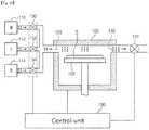
- FIG. 10 illustrates an apparatus of forming a layer by pressure-assisted deposition according to one embodiment of the present invention.
- an apparatus of forming a layer by pressure-assisted deposition may comprise a chamber 100.
- the accommodating space of the chamber 100 may be provided with a stage 102 on which a substrate is mounted.
- the chamber 100 may have an inlet 120 configured to sequentially receive source gas, inert gas, reactive gas and inert gas, and an outlet configured to discharge the received gas.
- the outlet 140 may be provided with a discharge valve 142 configured to control discharge rate.
- the layer forming apparatus may further comprise a source gas storage unit 110 configured to store source gas, an inert gas storage unit 112 configured to store inert gas, and a reactive gas storage unit 114 configured to store reactive gas.
- the source gas storage unit 110 may store a source gas corresponding to the type of layer to be deposited.
- the source gas storage unit 110 may store DEZ.
- the inert gas storage unit 112 may store argon or nitrogen gas, and the reactive gas storage unit 110 may store a gas corresponding to the source gas.
- the metal precursor gas stored in the source gas storage unit 110 may be supplied to the inlet 120 of the chamber 100 through a source gas control valve 130.
- the inert gas stored in the inert gas storage unit 112 may be supplied to the inlet 120 of the chamber 100 through an inert gas control valve 132.
- the reactive gas stored in the reactive gas storage unit 114 may be supplied to the inlet 120 of the chamber 100 through a reactive gas control valve 134.
- the apparatus of forming a layer by pressure-assisted deposition may further comprise a control unit 150.
- the control unit 150 may be configured to perform the layer forming method according to one embodiment of the present invention by controlling each element.
- control unit 150 may be configured to control the source gas control valve 130, the inert gas control valve 132 and the reactive gas control valve 134 such that source gas, inert gas, reactive gas and inert gas are sequentially supplied to the inlet 120 of the chamber 100.
- the control unit 150 may open the source gas control valve 130 and close the discharge valve 142. Accordingly, when the source gas is supplied to the inside of the chamber 100, the pressure in the chamber may increase to a predetermined pressure. Next, the control unit 150 may also close the source gas control valve 130. Accordingly, the chamber 100 may be closed. This can maintain the inside of the chamber 100 at high pressure, thereby significantly increasing the adsorption rate of the source gas. Namely, the control unit 150 can control the internal pressure of the chamber, thereby improving the step coverage of the layer formed of the source gas adsorbed on the substrate surface. For step S130, the control unit 150 may perform control in the same manner as described above.
- the control unit 150 may control the source gas control valve 130 and the discharge valve 142.
- the control unit 150 may provide a pressure for at least two sub-dosing/pressurizing steps and a pressure for a sub-purging step between the at least two sub-dosing/pressurizing steps.
- the pressure that has been increased by the sub-dosing/pressurizing step may be maintained through the sub-exposure step.
- control unit 150 may maintain the temperature in the chamber at a constant level when source gas, inert gas or reactive gas is dosed into the chamber.
- the control unit 150 may control the temperature in the chamber to a temperature of 80°C to 250°C, for example.
- one embodiment of the present invention is used for deposition of the metal oxide layer
- one embodiment of the present invention may also be applied for deposition of a layer other than the metal oxide layer, for example, a dielectric layer, particularly a silicon-containing dielectric layer.
- FIG. 11 is a flow chart illustrating a method of fabricating a metal oxide transistor according to one embodiment of the present invention
- FIG. 12 illustrates a metal oxide transistor according to one embodiment of the present invention.
- a method of fabricating a metal oxide transistor may comprise at least one of the steps of: (S200) preparing a substrate; (S210) forming a gate electrode and a gate insulating layer; (S220) forming an active layer including a metal oxide layer; and (S230) forming source and drain electrodes.
- Step S220 may comprise the steps S110, S120 S130 and S140 described above with reference to FIG. 1 .
- the metal oxide layer may be used as the active layer of the transistor.
- the metal oxide transistor may comprise: a substrate 210; a gate electrode 220 formed on one side of the substrate; a gate insulating layer 230 formed on one side of the gate electrode; a metal oxide-containing active layer 240 formed on one side of the gate insulating layer; and a source electrode 252 and drain electrode 254 formed on one side of the active layer 240.
- the active layer 240 comprises a metal oxide layer.
- the thickness of the metal oxide layer may be, for example, greater than 1.5 nm.
- the thickness of the metal oxide layer may be greater than 1.5 run and not greater than 7 nm.
- the thickness of the metal oxide layer may be greater than 1.5 nm and not greater than 5 nm.
- the number of cycles for deposition of the metal oxide layer may be greater than 7.
- the number of cycles for deposition of the metal oxide layer may be greater than 7 and not greater than 35.
- the number of cycles for deposition of the metal oxide layer may be greater than 7 and not greater than 25.
- the surface roughness (RMS) of the metal oxide layer may be less than 4.4 ⁇ .
- a metal oxide transistor according to one embodiment of the present invention may also be fabricated as a top gate-type, dual gate-type or coplanar-type transistor.
- the sequence of the steps S200 to S230 described above with reference to FIG. 12 may vary depending on the type of transistor.
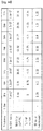
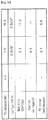
- FIG. 13 shows the results of measuring the FET characteristics of metal oxide transistors fabricated according to one embodiment of the present invention. Specifically, FIGS. 13a to 13i show current-voltage (I-V) curves depending on the thickness of the metal oxide layer (i.e., zinc oxide layer). FIG. 14 quantitatively shows the FET characteristic measurement results shown in FIG. 13 .
- I-V current-voltage
- metal oxide transistors were fabricated using the metal oxide layer forming process described above with reference to FIG. 4(a) .
- metal oxide layers were deposited to thicknesses of 1.5 nm, 3 nm, 4 run, 5 nm, 6 nm, 7 nm 8 nm, 9 nm and 10 nm by changing the number of cycles of the unit process.
- the thickness of the metal oxide layer was 1.5 nm, no FET (field effect transistor) characteristic appeared.
- the thickness of the metal oxide layer be greater than 1.5 nm in view of the FET characteristics. In other words, it is preferable that the number of cycles for deposition of the metal oxide layer be greater than 7.
- the thickness of the metal oxide layer was greater than 1.5 nm, it could be seen that stable FET characteristics appeared. Namely, when the thickness of the metal oxide layer was greater than 1.5 nm, it could be seen that on/off ratio characteristics, mobility characteristics, threshold voltages and SS values appeared.
- the thickness of the metal oxide layer be 7 nm or less in view of the mobility.
- the number of cycles for deposition of the metal oxide layer be 35 or less. This is because increasing the number of process cycles for deposition of the metal oxide layer may reduce the economy of the process without further improving the mobility characteristics.
- the on/off ratio characteristics were improved.
- the thickness of the metal oxide layer was 7 nm or less, the on/off ratio exceeded 10 6 which is a common level.
- the metal oxide transistor according to one embodiment of the present invention has been described above with reference to FIGS. 13 and 14 .
- a metal oxide transistor according to a conventional art will be described with reference to FIGS. 15 and 16 .
- FIG. 15 shows the results of measuring the FET characteristics of metal oxide transistors fabricated according to a conventional art
- FIG. 16 quantitatively show the FET characteristic measurement results shown in FIG. 15 .
- metal oxide transistors were fabricated using the metal oxide layer forming process described above with reference to FIG. 4(b) .
- metal oxide layers were deposited to thicknesses of 4 nm, 5 nm and 10 nm by changing the number of cycles of the process.
- the metal oxide transistors fabricated according to the conventional art showed no FET characteristic even when the thickness of the metal oxide layer was 4 nm.
- the thickness of the metal oxide layer in the metal oxide transistor fabricated according to one embodiment of the present invention was 5 nm, the mobility reached 30.05 cm 2 /Vs, but when the thickness of the metal oxide layer in the metal oxide transistor fabricated according to the conventional art was 5 nm, the mobility was only 2.1 cm 2 /Vs.
- the metal oxide transistor according to one embodiment of the present invention exhibits FET characteristics and better transistor characteristics, even when the metal oxide layer therein has a thinner thickness.
- the method of forming a metal oxide layer by pressure-assisted deposition according to one embodiment of the present invention can form a high-quality metal oxide layer.
- the method of forming a layer according to one embodiment of the present invention can exhibit not only high growth rate, but also excellent surface morphology.
- a metal oxide transistor fabricated based on the method of forming a metal oxide layer by pressure-assisted deposition according to one embodiment of the present invention and the method of fabricating the metal oxide transistor exhibit FET characteristics even when the thickness of the metal oxide layer is very thin.
Landscapes
- Chemical & Material Sciences (AREA)
- General Chemical & Material Sciences (AREA)
- Chemical Kinetics & Catalysis (AREA)
- Engineering & Computer Science (AREA)
- Materials Engineering (AREA)
- Mechanical Engineering (AREA)
- Metallurgy (AREA)
- Organic Chemistry (AREA)
- Inorganic Chemistry (AREA)
- Thin Film Transistor (AREA)
- Chemical Vapour Deposition (AREA)
- Formation Of Insulating Films (AREA)
Abstract
Description
- The present invention relates to a method and an apparatus for forming a layer, a metal oxide transistor and a fabrication method thereof.
- As the development of processes for fabricating scale-down elements has become more intense, various studies on the deposition of better layers, for example, metal oxide layers, have been conducted.
- Metal oxides are currently widely used in various electronic semiconductor devices. They are typically used as active layers or dielectric layers for devices, and various studies on processes for depositing them have also been conducted.
- In conventional processes of forming metal oxide layers by atomic layer deposition, there are limitations in forming an inorganic thin layer having high step coverage with a very thin thickness of a few nm. In addition, when liquid phase processes are used, there are difficulties in obtaining reproducible samples, difficulties in achieving large area fabrication, difficulties in achieving precise thickness control, difficulties in selecting a proper solvent that do not interacts with a substrate while dissolving a solute, and limitations in commercialization.
- It is an object of the present invention to provide a method and an apparatus for forming a layer, which are capable of depositing a layer in a simple and easy manner.
- Another object of the present invention is to provide a method and an apparatus for forming a good-quality layer.
- Still another object of the present invention is to provide a method and an apparatus for forming a layer, which can deposit a layer through a low-temperature process.
- Still another object of the present invention is to provide a method and an apparatus for forming a layer, which can easily control the layer thickness.
- Still another object of the present invention is to provide a method and an apparatus for forming a layer, which can deposit a layer at high rate.
- Still another object of the present invention is to provide a method and an apparatus for forming a layer having an excellent surface morphology.
- Still another object of the present invention is to provide a metal oxide transistor having an active layer including a metal oxide layer, and a method for fabricating the same.
- Still another object of the present invention is to provide a metal oxide transistor having high mobility, and a method for fabricating the same.
- Still another object of the present invention is to provide a metal oxide transistor having high on/off ratio, and a method for fabricating the same.
- However, objects which are to be achieved by the present invention are not limited to the above-mentioned objects, and other objects of the present invention will be clearly understood by those skilled in the art from the following description.
- A layer forming method according to one embodiment of the present invention may comprise: a source gas dosing/pressurizing step of dosing a source gas into a chamber having a substrate loaded therein in a state in which the outlet of the chamber is closed, thereby increasing the pressure in the chamber and adsorbing the source gas onto the substrate; a first main purging step of purging the chamber, after the source gas dosing/pressurizing step; a reactive gas dosing step of dosing a reactive gas into the chamber, after the first main purging step; and a second main purging step of purging the chamber, after the reactive gas dosing step.
- According to one embodiment, the source gas dosing/pressurizing step may further comprise the steps of: increasing the pressure in the chamber to a predetermined pressure by dosing the source gas; and maintaining the predetermined pressure by closing the inlet of the chamber.
- According to one embodiment, the source gas dosing/pressurizing step may comprise at least two sub-dosing/pressurizing steps and a sub-purging step between the at least two sub-dosing/pressurizing steps.
- According to one embodiment, the source gas dosing/pressurizing step may further comprise, between the sub-dosing/pressurizing step and the sub-purging step, a step of maintaining the chamber pressure that has been increased by the sub-dosing/pressurizing step.
- According to one embodiment, the reactive gas dosing step may further comprise the steps of: increasing the pressure in the chamber to a predetermined pressure by dosing the reactive gas; and maintaining the predetermined pressure by closing the inlet of the chamber.
- According to one embodiment, the reactive gas dosing step may comprise at least two sub-dosing/pressurizing steps and a sub-purging step between the at least two sub-dosing/pressurizing steps.
- According to one embodiment, the reactive gas dosing step may further comprise, between the sub-dosing/pressurizing step and the sub-purging step, a step of maintaining the chamber pressure that has been increased by the sub-dosing/pressurizing step.
- According to one embodiment, the source gas may comprise a metal precursor for forming a metal oxide layer by deposition.
- According to one embodiment, the metal oxide layer, formed by the source gas dosing/pressurizing step, the first main purging step, the reactive gas dosing step and the second purging step, may have a surface roughness (RMS) lower than 4.4Å.
- According to one embodiment, the metal oxide layer, formed by the source gas dosing/pressurizing step, the first main purging step, the reactive gas dosing step and the second purging step, may comprise a plurality of crystalline regions, and an amorphous region surrounding the crystalline regions.
- According to one embodiment, each of the crystalline regions may have a nanometer size.
- A layer forming apparatus according to one embodiment of the present invention may comprise: an inlet configured to supply a source gas, an inert gas and a reactive gas; a chamber configured to communicate with the inlet and accommodate a substrate; an outlet configured to discharge the gases supplied into the chamber; and a control unit configured to close the outlet when the source gas is supplied into the chamber, thereby increasing the pressure in the chamber and adsorbing the source gas onto the substrate.
- According to one embodiment, the control unit may be configured to close the inlet of the chamber when the pressure in the chamber reaches a predetermine pressure, and to maintain the closed state for a predetermined time.
- According to one embodiment, the control unit may be configured to provide a pressure for at least two sub-dosing/pressurizing steps and a pressure for a sub-purging step between the at least two sub-dosing/pressurizing steps.
- According to one embodiment, the source gas may comprise a metal oxide precursor for metal oxide deposition.
- A metal oxide transistor according to one embodiment of the present invention may comprise: a gate electrode; a gate insulating layer formed on one side of the gate electrode; an active layer formed on one side of the gate insulating layer and including a metal oxide layer; and source and drain electrodes provided on one side of the active layer.
- According to one embodiment, the thickness of the metal oxide layer may be greater than 1.5 nm.
- According to one embodiment, the thickness of the metal oxide layer may be greater than 1.5 nm and not greater than 7 nm.
- According to one embodiment, the thickness of the metal oxide layer may be greater than 1.5 nm and smaller than 5.0 nm.
- According to one embodiment, the surface roughness (RMS) of the metal oxide layer may be lower than 4.4 Å.
- A method of fabricating a metal oxide transistor according to one embodiment of the present invention may comprise the steps of: preparing a substrate; and forming an active layer including a metal oxide layer on one side of the substrate, wherein the step of forming the active layer may comprise: a source gas dosing/pressurizing step of dosing a source gas for metal oxide deposition into a chamber having the substrate loaded therein in a state in which the outlet of the chamber is closed, thereby increasing the pressure in the chamber and adsorbing the source gas onto the substrate in the closed chamber; a first main purging step of purging the chamber, after the source gas dosing/pressurizing step; a reactive gas dosing step of dosing a reactive gas into the chamber, thereby depositing a metal oxide layer onto the substrate, after the first main purging step; and a second main purging step of purging the chamber, after the reactive gas dosing step.
- According to one embodiment, the source gas dosing/pressurizing step, the first main purging step, the reactive gas dosing step and the second main purging step may constitute a unit process, and the electrical properties of the active layer is variable depending on the number of repetitions of the unit process.
- According to one embodiment, the number of repetitions of the unit process may be greater than 7 and not greater than 35 when the metal oxide layer comprises zinc oxide.
- According to one embodiment, the source gas dosing/pressurizing step may comprise at least two sub-dosing/pressurizing steps and a sub-purging step between the at least two sub-dosing/pressurizing steps.
- According to one embodiment, the magnitude of a pressure for each of the at least two sub-dosing/pressurizing steps may increase depending on the number of repetition of the sub-dosing/pressurizing step.
- According to one embodiment, the source gas dosing/pressurizing step may comprise at least two sub-dosing/pressurizing steps and a sub-purging step between the at least two sub-dosing/pressurizing steps; the reactive gas dosing step may further comprise at least two sub-dosing/pressurizing steps and a sub-purging step between the at least two sub-dosing/pressurizing steps; and the time of the sub-purging step of the source gas dosing/pressurizing step may be shorter than that of the sub-purging step of the reactive gas dosing step.
- According to one embodiment, the source gas may comprise diethyl zinc (DEZ), and the reactive gas may comprise H2O.
- According to one embodiment, the source gas dosing/pressurizing step, the first main purging step, the reactive gas dosing step and the second main purging step may constitute a unit process, and the unit process may be repeated in a predetermined number.
- According to one embodiment, the predetermined number may be greater than 7.
- According to one embodiment, the source gas dosing/pressurizing step may further comprise, after increasing the pressure in the chamber by dosing the source gas, an exposure step of maintaining the increased pressure for a predetermined time.
- A method and apparatus of forming a layer according to one embodiment of the present invention may provide a good-quality layer while depositing the layer in a simple and easy manner.
- A method and apparatus of forming a layer according to one embodiment of the present invention can deposit a layer at low temperature.
- A method and apparatus of forming a layer according to one embodiment of the present invention can easily control the layer thickness.
- A method and apparatus of forming a layer according to one embodiment of the present invention can provide a good-quality layer at high deposition rate.
- A method and apparatus of forming a layer according to one embodiment of the present invention may provide a layer having excellent surface morphology.
- A metal oxide transistor and a fabrication method thereof according to an embodiment of the present invention can exhibit excellent FET characteristics.
- A metal oxide transistor and a fabrication method thereof according to an embodiment of the present invention can exhibit FET characteristics even when a metal oxide layer therein has a very thin thickness.
- The technical effects of the present invention are not limited to the above-mentioned effects, and other effects of the present invention will be clearly understood by those skilled in the art from the following description.
-
-
FIG. 1 illustrates a method of forming a layer according to one embodiment of the present invention. -
FIGS. 2 and3 illustrate step S10 according to one embodiment of the present invention. -
FIG. 4 shows process conditions according to one embodiment of the present invention. -
FIGS. 5 and6 show the result of measuring layer growth rate in each of a conventional art and one embodiment of the present invention. -
FIGS. 7 and8 shows the results of measuring the surface roughness of each of a layer formed according to a conventional art and a layer formed according to one embodiment of the present invention. -
FIG. 9 is an image showing the crystal characteristic of a layer formed according to one embodiment of the present invention. -
FIG. 10 illustrates a layer forming apparatus according to one embodiment of the present invention. -
FIG. 11 is a flow chart illustrating a method of fabricating a metal oxide transistor according to one embodiment of the present invention. -
FIG. 12 illustrates a metal oxide transistor according to one embodiment of the present invention. -
FIG. 13 shows the results of measuring the FET characteristics of metal oxide transistors fabricated according to one embodiment of the present invention. -
FIG. 14 quantitatively shows the FET characteristic measurement results shown in FIG.
13. -
FIG. 15 shows the results of measuring the FET characteristics of metal oxide transistors fabricated according to a conventional art. -
FIG. 16 quantitatively shows the FET characteristic measurement results shown inFIG. 15 . - Hereinafter, exemplary embodiments of the present invention will be described in detail with reference to the accompanying drawings. The present invention may, however, be embodied in different forms and should not be construed as limited to the embodiments set forth herein. Rather, these embodiments are provided so that this disclosure will be thorough and complete, and will fully convey the scope of the present invention to those skilled in the art.
- In the specification, when any element is referred to as being "on" other element, it means that the element may be formed directly on the other element, or that a third element may be interposed therebetween. In the drawings, the thicknesses of layers and regions may have been exaggerated in order to clearly illustrate features of the embodiments.
- In addition, although the terms 'first', 'second', "third" etc. may be used to describe various elements in various embodiments of the present invention, these elements should not be limited by these terms. These terms are only used to distinguish any element from other element. Thus, a first element mentioned in any one embodiment may be termed a second element in other embodiment. Each embodiment described and exemplified herein also includes a complementary embodiment thereof As used herein, the term "and/or" is meant to include at least one of components listed before and after the term "and/or".
- In the specification, singular expressions include plural expressions unless specified otherwise in the context thereof In addition, the terms "comprise", "have", etc., are intended to denote the existence of mentioned characteristics, numbers, steps, elements, components, or combinations thereof, but do not exclude the probability of existence or addition of one or more other characteristics, numbers, steps, elements, components, or combinations thereof As used herein, the term "connecting" includes connecting a plurality of elements both directly and indirectly.
- Furthermore, in the following description, detailed description of related known functions and configurations will be omitted when it may unnecessarily obscure the subject matter of the present invention.
-
FIG. 1 illustrates a method of forming a layer according to one embodiment of the present invention, andFIGS. 2 and3 illustrate step S110 according to one embodiment of the present invention. - Referring to
FIG. 1 , a method of forming a layer by pressure-assisted deposition according to one embodiment of the present invention may comprise at least one of a source gas dosing/pressurizing step (S110), a first main purging step (S120), a reactive gas dosing step (S130), and a second main purging step (S140). Hereinafter, each of the method will be described. - For the source gas dosing/pressurizing step (S110), a source gas may be prepared. The kind of source gas to be prepared may vary depending on the type of layer to be deposited. For example, when a layer to be deposited is a metal oxide layer, a metal precursor source gas corresponding thereto may be prepared. For example, when a layer to be deposited is a zinc oxide (ZnO) layer, the source gas may comprise DEZ (diethyl zinc).
- The source gas may be dosed into a chamber in a state in which the chamber outlet is closed. Accordingly, as the source gas is dosed into the chamber, the pressure in the chamber can increase. In other words, the pressure in the chamber is increased by dosing of the source gas, and hence the source gas may be adsorbed onto a substrate in a pressurized atmosphere.
- The increased pressure in step S110 may be higher than 0.03 Torr, preferably, 0.1 Torr or higher, and more preferably 0.3 Torr or higher. In addition, step S110 may be performed at a temperature of 20°C to 250°C.
- In the first main purging step (S120), inert gas may be used. The inert gas may be, for example, argon (Ar) or nitrogen (N2) gas. Through the purging step, an excess of the source gas that has not been absorbed onto the substrate surface may be removed.
- In the reactive gas dosing step (S130), a reactive gas may react with the source gas to form the layer to be deposited. For example, when the source gas comprises DEZ, the reactive gas may comprise H2O.
- After the reactive gas dosing step, the second main purging step (S140) may further be performed. This can remove an excess of the gas that has not been adsorbed onto the substrate surface.
- Step S110 to step S140 according to one embodiment of the present invention have been described above. Hereinafter, dosing/pressurizing of step S110 will be described in detail.
- The source gas dosing/pressurizing step (step S110) may be performed in a pressurized atmosphere. In other words, the source gas dosing/pressurizing step may be performed in a high-pressure atmosphere, and may be abbreviated as "pressurizing step".
- Although the source gas dosing/pressurizing step (step S110) will be described in detail for the sake of brevity, it should be understood that dosing/pressurizing may also be performed in the reactive gas dosing step (step S130).
- According to one embodiment, the dosing/pressurizing step may be performed in a state in which a chamber having a substrate loaded therein is closed. For example, the discharge valve of a chamber is closed, and in this state, a metal precursor source gas may be dosed into the chamber (sub-dosing/pressurizing step), thereby inducing high pressure in the chamber, and the induced high pressure may be maintained (sub-exposure step). When the high pressure is maintained for a predetermined time, the metal precursor source gas may be adsorbed onto the substrate surface in a high-pressure atmosphere.
- According to one embodiment, the dosing/pressurizing step may comprise at least one of a sub-dosing/pressurizing step, a sub-exposure step and a sub-purging step. The sub-dosing/pressurizing step may be defined as a step of dosing the source gas into the chamber in a state in which the outlet of the chamber is closed, thereby causing the pressure in the chamber to reach a predetermined pressure. The sub-exposure step is a step of maintaining the predetermined pressure provided by the sub-dosing/pressurizing step. To this end, the inlet and outlet of the chamber may all be closed. Namely, the chamber may be closed. The sub-purging step may be performed after the sub-exposure step to remove an excess of the source gas dosed.
- As shown in
FIG. 2 , the pressure in the sub-exposure step may be maintained at a constant level, even when the number of the sub-exposure steps increases. Unlike this, as shown inFIG. 3 , the pressure in the sub-exposure step may increase as the number of the sub-exposure steps increases. - According to one embodiment, step S110 may be performed at a temperature of 80°C to 250°C.
- In addition, sub-steps of step S110 may be performed at the same temperature. In particular, these sub-steps may be performed at low temperature. As used herein, the term "low temperature" refers to a temperature of 250°C or below, preferably 80°C to 250°C.
- The layer forming method according to one embodiment of the present invention has been described above with reference to
FIGS. 1 to 3 . Hereinafter, the performance characteristics of a layer formed according to one embodiment of the present invention will be described. -
FIG. 4 shows process conditions according to one embodiment of the present invention;FIGS. 5 and6 show the results of measuring layer growth rate in each of a conventional art and one embodiment of the present invention;FIGS. 7 and8 show the results of measuring the surface roughness of each of a layer formed according to a conventional art and a film formed according to one embodiment of the present invention; andFIG. 9 is an image showing the crystal characteristics of a layer formed according to one embodiment of the present invention. - As shown in
FIG. 4 , a zinc oxide layer which is a metal oxide layer was formed according to one embodiment of the present invention. The layer forming method is as described above with respect toFIG. 1 . - Specifically, referring to
FIG. 4(a) , in step S110, DEZ was dosed by performing sub-dosing/pressurizing dosing five times. Specifically, in the first sub-dosing/pressurizing step, DEX was dosed into a chamber containing a substrate in a state in which the outlet of the chamber was closed, thereby increasing the pressure in the chamber to 1.0 Torr. Next, the inlet of the chamber was also closed, and in this state, DEZ was adsorbed onto the substrate by substrate exposure to DEZ at a pressure of 1.0 Torr for 3 seconds (sub-exposure step). Then, sub-purging was performed for 30 seconds. Next, in the second sub-dosing/pressurizing step, DEZ was dosed into the chamber in a state in which the outlet of the chamber was closed, thereby increasing the pressure in the chamber to 1.0 Torr. Next, the inlet of the chamber was also closed, and in this state, DEZ was adsorbed onto the substrate by substrate exposure to DEZ at a pressure of 1.0 Torr for 3 seconds. In this manner, sub-dosing and sub-exposure were repeated five times. - Next, according to step S120, a first main purging step was performed for 15 seconds.
- In step S130, H2O was dosed by performing sub-dosing/pressurizing and sub-exposure five times. In this step, process parameters, such as pressure and time, were the same as those used in DEZ dosing.
- According to one embodiment, each of step S110 and S130 may comprise at least two sub-dosing/pressurizing steps and a sub-purging step between the at least two sub-dosing/pressurizing steps. In this case, the time of the sub-purging step in step S110 may be shorter than the time of the sub-purging step in step S130. This is because the reactive gas H2O is more likely to aggregate than the source gas DEZ.
- A unit cycle composed of the above-described steps was repeatedly performed, thereby controlling the thickness of the zinc oxide, a metal oxide.
- In order to confirm the superiority of the zinc oxide layer formed according to one embodiment of the present invention, a zinc oxide layer according to a conventional art was formed.
- The "zinc oxide layer according to a conventional art" refers to a metal oxide layer formed according to a conventional atomic deposition process.
- Specifically, referring to
FIG. 4(b) , in order to form a metal oxide layer according to a conventional art, a DEZ source gas was supplied to a chamber at a pressure of 30 mTorr for 2 seconds, and the chamber was purged for 20 seconds, after which a H2O reactive gas was supplied to the chamber at a pressure of 30 mTorr for 2 seconds, followed by purging for 40 seconds. A unit cycle composed of these steps was repeatedly performed. - Referring to
FIG. 5 , it was confirmed that the method of forming a metal oxide layer by pressure-assisted deposition according to one embodiment of the present invention as shown inFIG. 4(a) showed a ZnO growth rate of 2.1 Å per cycle. - Unlike this, referring to
FIG. 6 , it was confirmed that the method of forming a metal oxide layer according to the conventional art as shown inFIG. 4(b) showed a ZnO growth rate of only 1.5 Å per cycle. This suggests that the layer forming method according to one embodiment of the present invention exhibits a higher layer growth rate than that of the conventional art. -
FIG. 7 shows the result of measuring the surface roughness of the metal oxide layer formed according to one embodiment of the present invention, andFIG. 8 shows the result of measuring the surface roughness of the metal oxide layer formed according to the conventional art. - To measure the surface roughness, the unit cycle descried above with reference to
FIG. 4 was performed 15 times. - Referring to
FIG. 7 , it was confirmed that the surface roughness (RMS) of the metal oxide layer formed according to one embodiment of the present invention was 2.3 Å, indicating that it has very good morphology. Unlike this, referring toFIG. 8 , the surface roughness (RMS) of the metal oxide layer formed according to the conventional art was 4.4Å. - This suggests that the layer forming method according to one embodiment exhibits better surface morphology than the conventional art.
-
FIG. 9 is an image showing the crystal characteristics of the layer formed according to one embodiment of the present invention. - To confirm the crystal characteristics of the layer, zinc oxide was first deposited to a thickness of 2.5 nm according to one embodiment of the present invention as described above with reference to
FIG. 4(a) . A TEM image of the zinc oxide layer formed was analyzed, and as a result, it was confirmed that crystalline regions (NC_R) and an amorphous region (AM_R) were present together in the zinc oxide layer. As shown inFIG. 9 , the crystalline regions (NC_R) were randomly distributed in a two-dimensional plane, and the amorphous region (AM_R) surrounded the crystalline regions (NC_R). Namely, the crystalline regions (NC_R) were composed of a plurality of island shapes. In addition, the crystalline regions (NC_R) were shown to have a size of about 3 nm. Accordingly, it is expected that the crystalline regions (NC_R) will have a quantum confinement effect. - The layer forming method according to one embodiment of the present invention has been described above. Hereinafter, a layer forming apparatus according to one embodiment of the present invention will be described with reference to
FIG. 10 . -
FIG. 10 illustrates an apparatus of forming a layer by pressure-assisted deposition according to one embodiment of the present invention. - Referring to
FIG. 10 , an apparatus of forming a layer by pressure-assisted deposition according to one embodiment of the present invention may comprise achamber 100. The accommodating space of thechamber 100 may be provided with astage 102 on which a substrate is mounted. - The
chamber 100 may have aninlet 120 configured to sequentially receive source gas, inert gas, reactive gas and inert gas, and an outlet configured to discharge the received gas. In addition, theoutlet 140 may be provided with adischarge valve 142 configured to control discharge rate. - In addition, the layer forming apparatus according to one embodiment of the present invention may further comprise a source
gas storage unit 110 configured to store source gas, an inertgas storage unit 112 configured to store inert gas, and a reactivegas storage unit 114 configured to store reactive gas. - Here, the source
gas storage unit 110 may store a source gas corresponding to the type of layer to be deposited. For example, when zinc oxide is to be deposited, the sourcegas storage unit 110 may store DEZ. - The inert
gas storage unit 112 may store argon or nitrogen gas, and the reactivegas storage unit 110 may store a gas corresponding to the source gas. - The metal precursor gas stored in the source
gas storage unit 110 may be supplied to theinlet 120 of thechamber 100 through a sourcegas control valve 130. The inert gas stored in the inertgas storage unit 112 may be supplied to theinlet 120 of thechamber 100 through an inert gas control valve 132. In addition, the reactive gas stored in the reactivegas storage unit 114 may be supplied to theinlet 120 of thechamber 100 through a reactivegas control valve 134. - In addition, the apparatus of forming a layer by pressure-assisted deposition according to one embodiment of the present invention may further comprise a
control unit 150. Thecontrol unit 150 may be configured to perform the layer forming method according to one embodiment of the present invention by controlling each element. - More specifically, the
control unit 150 may be configured to control the sourcegas control valve 130, the inert gas control valve 132 and the reactivegas control valve 134 such that source gas, inert gas, reactive gas and inert gas are sequentially supplied to theinlet 120 of thechamber 100. - For step S110 (shown in
FIG. 1 ), thecontrol unit 150 may open the sourcegas control valve 130 and close thedischarge valve 142. Accordingly, when the source gas is supplied to the inside of thechamber 100, the pressure in the chamber may increase to a predetermined pressure. Next, thecontrol unit 150 may also close the sourcegas control valve 130. Accordingly, thechamber 100 may be closed. This can maintain the inside of thechamber 100 at high pressure, thereby significantly increasing the adsorption rate of the source gas. Namely, thecontrol unit 150 can control the internal pressure of the chamber, thereby improving the step coverage of the layer formed of the source gas adsorbed on the substrate surface. For step S130, thecontrol unit 150 may perform control in the same manner as described above. - For the sub-pressurizing step shown in
FIGS. 2 and3 , thecontrol unit 150 may control the sourcegas control valve 130 and thedischarge valve 142. Thus, when thecontrol unit 150 doses the source gas into the chamber, it may provide a pressure for at least two sub-dosing/pressurizing steps and a pressure for a sub-purging step between the at least two sub-dosing/pressurizing steps. In addition, the pressure that has been increased by the sub-dosing/pressurizing step may be maintained through the sub-exposure step. - Furthermore, the
control unit 150 may maintain the temperature in the chamber at a constant level when source gas, inert gas or reactive gas is dosed into the chamber. Thecontrol unit 150 may control the temperature in the chamber to a temperature of 80°C to 250°C, for example. - Although it has been described that one embodiment of the present invention is used for deposition of the metal oxide layer, one embodiment of the present invention may also be applied for deposition of a layer other than the metal oxide layer, for example, a dielectric layer, particularly a silicon-containing dielectric layer.
- Hereinafter, a method of fabricating a metal oxide transistor according to one embodiment of the present invention and a metal oxide transistor fabricated thereby will be described.
-
FIG. 11 is a flow chart illustrating a method of fabricating a metal oxide transistor according to one embodiment of the present invention, andFIG. 12 illustrates a metal oxide transistor according to one embodiment of the present invention. - Referring to
FIG. 11 , a method of fabricating a metal oxide transistor according to one embodiment of the present invention may comprise at least one of the steps of: (S200) preparing a substrate; (S210) forming a gate electrode and a gate insulating layer; (S220) forming an active layer including a metal oxide layer; and (S230) forming source and drain electrodes. - Step S220 may comprise the steps S110, S120 S130 and S140 described above with reference to
FIG. 1 . Namely, the metal oxide layer may be used as the active layer of the transistor. - Through this method, a metal oxide transistor according to one embodiment of the present invention as shown in
FIG. 12 can be fabricated. Referring toFIG. 12 , the metal oxide transistor may comprise: asubstrate 210; agate electrode 220 formed on one side of the substrate; agate insulating layer 230 formed on one side of the gate electrode; a metal oxide-containingactive layer 240 formed on one side of the gate insulating layer; and asource electrode 252 anddrain electrode 254 formed on one side of theactive layer 240. - The
active layer 240 comprises a metal oxide layer. When the metal oxide layer comprises zinc oxide, the thickness of the metal oxide layer may be, for example, greater than 1.5 nm. As another example, the thickness of the metal oxide layer may be greater than 1.5 run and not greater than 7 nm. As still another example, the thickness of the metal oxide layer may be greater than 1.5 nm and not greater than 5 nm. In another aspect, the number of cycles for deposition of the metal oxide layer may be greater than 7. As another example, the number of cycles for deposition of the metal oxide layer may be greater than 7 and not greater than 35. As still another example, the number of cycles for deposition of the metal oxide layer may be greater than 7 and not greater than 25. In another aspect, the surface roughness (RMS) of the metal oxide layer may be less than 4.4Å. - Although the bottom gate-type metal oxide transistor has been described above with reference to
FIG. 12 , a metal oxide transistor according to one embodiment of the present invention may also be fabricated as a top gate-type, dual gate-type or coplanar-type transistor. In this case, the sequence of the steps S200 to S230 described above with reference toFIG. 12 may vary depending on the type of transistor. - Hereinafter, the FET characteristics of the metal oxide transistor according to one embodiment of the present invention will be described with reference to
FIGS. 13 and14 . -
FIG. 13 shows the results of measuring the FET characteristics of metal oxide transistors fabricated according to one embodiment of the present invention. Specifically,FIGS. 13a to 13i show current-voltage (I-V) curves depending on the thickness of the metal oxide layer (i.e., zinc oxide layer).FIG. 14 quantitatively shows the FET characteristic measurement results shown inFIG. 13 . - For the measurement results shown in
FIGS. 13 and14 , metal oxide transistors were fabricated using the metal oxide layer forming process described above with reference toFIG. 4(a) . In this case, metal oxide layers were deposited to thicknesses of 1.5 nm, 3 nm, 4 run, 5 nm, 6 nm, 7 nm 8 nm, 9 nm and 10 nm by changing the number of cycles of the unit process. - As a result, it could be seen that when the thickness of the metal oxide layer was 1.5 nm, no FET (field effect transistor) characteristic appeared. Hence, it is preferable that the thickness of the metal oxide layer be greater than 1.5 nm in view of the FET characteristics. In other words, it is preferable that the number of cycles for deposition of the metal oxide layer be greater than 7.
- When the thickness of the metal oxide layer was greater than 1.5 nm, it could be seen that stable FET characteristics appeared. Namely, when the thickness of the metal oxide layer was greater than 1.5 nm, it could be seen that on/off ratio characteristics, mobility characteristics, threshold voltages and SS values appeared.
- In particular, referring to
FIG. 14 , it can be seen that the mobility continuously increased until the thickness of the metal oxide layer reached 7 nm, and the mobility decreased at thicknesses of 8 nm, 9 nm and 10 nm. Thus, it is preferable that the thickness of the metal oxide layer be 7 nm or less in view of the mobility. In other words, it is preferable that the number of cycles for deposition of the metal oxide layer be 35 or less. This is because increasing the number of process cycles for deposition of the metal oxide layer may reduce the economy of the process without further improving the mobility characteristics. - In addition, referring to
FIG. 14 , it can be seen that when the thickness of the metal oxide layer was greater than 1.5 nm, the on/off ratio characteristics were improved. In particular, it can be seen that when the thickness of the metal oxide layer was 7 nm or less, the on/off ratio exceeded 106 which is a common level. - The metal oxide transistor according to one embodiment of the present invention has been described above with reference to
FIGS. 13 and14 . Hereinafter, a metal oxide transistor according to a conventional art will be described with reference toFIGS. 15 and16 . -
FIG. 15 shows the results of measuring the FET characteristics of metal oxide transistors fabricated according to a conventional art, andFIG. 16 quantitatively show the FET characteristic measurement results shown inFIG. 15 . - For the measurement results shown in
FIGS. 15 and16 , metal oxide transistors were fabricated using the metal oxide layer forming process described above with reference toFIG. 4(b) . In this case, metal oxide layers were deposited to thicknesses of 4 nm, 5 nm and 10 nm by changing the number of cycles of the process. - As shown in
FIGS. 15 and16 , it can be seen that the metal oxide transistors fabricated according to the conventional art showed no FET characteristic even when the thickness of the metal oxide layer was 4 nm. - In addition, it can be seen that when the thickness of the metal oxide layer in the metal oxide transistor fabricated according to one embodiment of the present invention was 5 nm, the mobility reached 30.05 cm2/Vs, but when the thickness of the metal oxide layer in the metal oxide transistor fabricated according to the conventional art was 5 nm, the mobility was only 2.1 cm2/Vs.
- Thus, it can be confirmed that the metal oxide transistor according to one embodiment of the present invention exhibits FET characteristics and better transistor characteristics, even when the metal oxide layer therein has a thinner thickness.
- As described above, the method of forming a metal oxide layer by pressure-assisted deposition according to one embodiment of the present invention can form a high-quality metal oxide layer. The method of forming a layer according to one embodiment of the present invention can exhibit not only high growth rate, but also excellent surface morphology.
- Furthermore, it can be seen that a metal oxide transistor fabricated based on the method of forming a metal oxide layer by pressure-assisted deposition according to one embodiment of the present invention and the method of fabricating the metal oxide transistor exhibit FET characteristics even when the thickness of the metal oxide layer is very thin.
- Although the present invention has been described above in detail with reference to exemplary embodiments thereof, the scope of the present invention is not limited to these embodiment and should be construed based on the appended claims. In addition, any person of ordinary skill in the art will appreciate that various modifications and alterations are possible without departing from the scope of the present invention.
Claims (4)
- A layer forming method comprising:a source gas dosing/pressurizing step of dosing a source gas into a chamber having a substrate loaded therein in a state in which an outlet of the chamber is closed, thereby increasing pressure in the chamber and adsorbing the source gas onto the substrate;a first main purging step of purging the chamber, after the source gas dosing/pressurizing step;a reactive gas dosing step of dosing a reactive gas into the chamber, after the first main purging step; anda second main purging step of purging the chamber, after the reactive gas dosing step.
- A layer forming apparatus comprising,
an inlet configured to supply a source gas, an inert gas and a reactive gas;
a chamber configured to communicate with the inlet and accommodate a substrate;
an outlet configured to discharge the gases supplied into the chamber; and
a control unit configured to close the outlet when the source gas is supplied into the chamber, thereby increasing pressure in the chamber and adsorbing the source gas onto the substrate. - A metal oxide transistor comprising:a gate electrode;a gate insulating layer formed on one side of the gate electrode;an active layer formed on one side of the gate insulating layer and including a metal oxide layer; andsource and drain electrodes provided on one side of the active layer.
- A method of fabricating a metal oxide transistor, comprising the steps of:preparing a substrate; andforming an active layer including a metal oxide layer on one side of the substrate,wherein the step of forming the active layer comprises:a source gas dosing/pressurizing step of dosing a source gas for metal oxide deposition into a chamber having the substrate loaded therein in a state in which an outlet of the chamber is closed, thereby increasing pressure in the chamber and adsorbing the source gas onto the substrate in the closed chamber;a first main purging step of purging the chamber, after the source gas dosing/pressurizing step;a reactive gas dosing step of dosing a reactive gas into the chamber, thereby depositing a metal oxide layer on the substrate, after the first main purging step; anda second main purging step of purging the chamber, after the reactive gas dosing step.
Applications Claiming Priority (2)
| Application Number | Priority Date | Filing Date | Title |
|---|---|---|---|
| KR20170134979 | 2017-10-18 | ||
| PCT/KR2018/012366 WO2019078652A1 (en) | 2017-10-18 | 2018-10-18 | Method for producing layer and apparatus for producing same, metal oxide transistor and method for producing same |
Publications (2)
| Publication Number | Publication Date |
|---|---|
| EP3686316A1 true EP3686316A1 (en) | 2020-07-29 |
| EP3686316A4 EP3686316A4 (en) | 2021-07-28 |
Family
ID=66281213
Family Applications (1)
| Application Number | Title | Priority Date | Filing Date |
|---|---|---|---|
| EP18810875.7A Pending EP3686316A4 (en) | 2017-10-18 | 2018-10-18 | LAYER PRODUCTION PROCESS AND APPARATUS FOR PRODUCING IT, METAL OXIDE TRANSISTOR AND ITS PRODUCTION PROCESS |
Country Status (4)
| Country | Link |
|---|---|
| US (2) | US11015243B2 (en) |
| EP (1) | EP3686316A4 (en) |
| JP (2) | JP6974363B2 (en) |
| KR (2) | KR102201378B1 (en) |
Families Citing this family (4)
| Publication number | Priority date | Publication date | Assignee | Title |
|---|---|---|---|---|
| KR101820237B1 (en) | 2016-04-29 | 2018-01-19 | 한양대학교 산학협력단 | Pressurized manufacturing method for metal monolayer, Structure for metal monolayer, Pressurized manufacturing apparatus for metal monolayer |
| KR20230024424A (en) | 2019-08-12 | 2023-02-20 | 커트 제이. 레스커 컴파니 | Ultra high purity conditions for atomic scale processing |
| US12577656B2 (en) | 2020-06-18 | 2026-03-17 | Regents Of The University Of Michigan | Transparent mesoporous materials and devices comprising same |
| CN119998491A (en) * | 2022-10-06 | 2025-05-13 | 朗姆研究公司 | Improve chemical utilization by increasing pressure during substrate processing |
Family Cites Families (24)
| Publication number | Priority date | Publication date | Assignee | Title |
|---|---|---|---|---|
| US5916365A (en) * | 1996-08-16 | 1999-06-29 | Sherman; Arthur | Sequential chemical vapor deposition |
| US6828218B2 (en) * | 2001-05-31 | 2004-12-07 | Samsung Electronics Co., Ltd. | Method of forming a thin film using atomic layer deposition |
| JP4817350B2 (en) * | 2001-07-19 | 2011-11-16 | 株式会社 東北テクノアーチ | Method for producing zinc oxide semiconductor member |
| KR20060093611A (en) | 2005-02-22 | 2006-08-25 | 삼성전자주식회사 | Chemical vapor deposition equipment and residual gas exhaust method |
| US7314835B2 (en) | 2005-03-21 | 2008-01-01 | Tokyo Electron Limited | Plasma enhanced atomic layer deposition system and method |
| KR100742644B1 (en) | 2006-01-05 | 2007-07-25 | 재단법인서울대학교산학협력재단 | Quantum dot formation method using monoatomic layer deposition |
| KR100811281B1 (en) * | 2006-12-27 | 2008-03-07 | 주식회사 테라세미콘 | Metal adsorption apparatus and method |
| JP4616359B2 (en) * | 2007-01-09 | 2011-01-19 | 韓國電子通信研究院 | Method for forming ZnO semiconductor film for electronic device and thin film transistor including the semiconductor film |
| JP4873726B2 (en) * | 2007-03-26 | 2012-02-08 | 独立行政法人物質・材料研究機構 | Method for forming zinc oxide thin film |
| US8017182B2 (en) * | 2007-06-21 | 2011-09-13 | Asm International N.V. | Method for depositing thin films by mixed pulsed CVD and ALD |
| KR100889020B1 (en) | 2007-08-14 | 2009-03-19 | 한양대학교 산학협력단 | Thin film transistor including multi-layered gate insulator |
| KR20090017073A (en) | 2007-08-14 | 2009-02-18 | 주식회사 아이피에스 | Silicon dioxide thin film manufacturing method using atomic layer thin film deposition |
| JP5073624B2 (en) * | 2008-09-16 | 2012-11-14 | スタンレー電気株式会社 | Method for growing zinc oxide based semiconductor and method for manufacturing semiconductor light emitting device |
| JP5638772B2 (en) | 2009-05-25 | 2014-12-10 | スタンレー電気株式会社 | Method for growing zinc oxide based semiconductor and method for manufacturing semiconductor light emitting device |
| JP5793723B2 (en) * | 2009-07-18 | 2015-10-14 | 高知県公立大学法人 | Thin film phosphor and method for forming the same |
| CN102763222A (en) * | 2010-12-27 | 2012-10-31 | 松下电器产业株式会社 | Field-effect transistor and method for manufacturing same |
| KR101309043B1 (en) * | 2012-01-31 | 2013-09-17 | 영남대학교 산학협력단 | Method for forming ruthenium thin film by atomic layer deposition and ruthenium thin film using the same |
| JP6150371B2 (en) * | 2012-05-31 | 2017-06-21 | 高知県公立大学法人 | Zinc oxide (ZnO) single crystal, ZnO thin film, method for producing ZnO single crystal thin film, ZnO single crystal thin film, and ZnO based material comprising the ZnO single crystal thin film |
| JP5918631B2 (en) * | 2012-06-04 | 2016-05-18 | Jswアフティ株式会社 | ZnO film forming method and ZnO film forming apparatus |
| JP5852151B2 (en) * | 2014-02-12 | 2016-02-03 | 株式会社日立国際電気 | Semiconductor device manufacturing method, substrate processing apparatus, program, and recording medium |
| JP5855691B2 (en) * | 2014-02-25 | 2016-02-09 | 株式会社日立国際電気 | Semiconductor device manufacturing method, substrate processing apparatus, program, and recording medium |
| KR102481037B1 (en) * | 2014-10-01 | 2022-12-27 | 가부시키가이샤 한도오따이 에네루기 켄큐쇼 | Wiring layer and manufacturing method therefor |
| KR101820237B1 (en) * | 2016-04-29 | 2018-01-19 | 한양대학교 산학협력단 | Pressurized manufacturing method for metal monolayer, Structure for metal monolayer, Pressurized manufacturing apparatus for metal monolayer |
| WO2018111247A1 (en) * | 2016-12-13 | 2018-06-21 | Intel Corporation | Passivation dielectrics for oxide semiconductor thin film transistors |
-
2018
- 2018-10-18 JP JP2018565745A patent/JP6974363B2/en active Active
- 2018-10-18 EP EP18810875.7A patent/EP3686316A4/en active Pending
- 2018-10-18 KR KR1020180124398A patent/KR102201378B1/en active Active
- 2018-10-18 KR KR1020180124418A patent/KR102214218B1/en active Active
- 2018-12-10 US US16/214,878 patent/US11015243B2/en active Active
-
2020
- 2020-10-21 JP JP2020176967A patent/JP2021021144A/en active Pending
-
2021
- 2021-04-20 US US17/235,002 patent/US11732354B2/en active Active
Also Published As
| Publication number | Publication date |
|---|---|
| US20190112704A1 (en) | 2019-04-18 |
| KR20190043486A (en) | 2019-04-26 |
| KR102201378B1 (en) | 2021-01-12 |
| US11015243B2 (en) | 2021-05-25 |
| KR102214218B1 (en) | 2021-02-10 |
| JP6974363B2 (en) | 2021-12-01 |
| JP2019537832A (en) | 2019-12-26 |
| US20210238738A1 (en) | 2021-08-05 |
| KR20190043488A (en) | 2019-04-26 |
| US11732354B2 (en) | 2023-08-22 |
| JP2021021144A (en) | 2021-02-18 |
| EP3686316A4 (en) | 2021-07-28 |
Similar Documents
| Publication | Publication Date | Title |
|---|---|---|
| US11732354B2 (en) | Method and apparatus for forming layer, metal oxide transistor and fabrication method thereof | |
| US9257272B2 (en) | Deposited material and method of formation | |
| US9064857B2 (en) | N metal for FinFET | |
| US7160817B2 (en) | Dielectric material forming methods | |
| US9496355B2 (en) | Conductive nanoparticles | |
| Kim et al. | Characteristics of ZrO 2 gate dielectric deposited using Zr t–butoxide and Zr (NEt 2) 4 precursors by plasma enhanced atomic layer deposition method | |
| US8741746B2 (en) | Silicon on germanium | |
| EP1136588A2 (en) | MOCVD method of tantalum oxide film | |
| US8481122B2 (en) | Methods of forming material over substrates | |
| WO2006026716A1 (en) | Atomic layer deposited titanium aluminum oxide films | |
| US7989290B2 (en) | Methods for forming rhodium-based charge traps and apparatus including rhodium-based charge traps | |
| US20060128127A1 (en) | Method of depositing a metal compound layer and apparatus for depositing a metal compound layer | |
| KR20180118541A (en) | Thin Film Transistor, and the Manufacturing Method of the same | |
| KR101827514B1 (en) | Thin film transistor and Method of manufacturing the same | |
| KR100996884B1 (en) | Semiconductor device with an oxide film manufactured by ERC-ALD method, method for manufacturing same, and use thereof | |
| KR20220155789A (en) | Method for depositing thin film | |
| CN110164878B (en) | Array substrate and preparation method thereof | |
| KR102430533B1 (en) | Semiconductor device including high dielectric constant aluminium oxide layer | |
| KR20240013974A (en) | Method for Manufacturing Thin Film, Thin Film, and Apparatus for Processing Substrate | |
| US20030215994A1 (en) | Method for forming ruthenium film of a semiconductor device | |
| KR20230115908A (en) | Method for Manufacturing Thin Film and Thin Film | |
| KR20060000877A (en) | Capacitor provided with hafnium nitride film and its manufacturing method | |
| KR20050011969A (en) | METHOD FOR FABRICATING La2O3 LAYER WITH ATOMIC LAYER DEPOSITION |
Legal Events
| Date | Code | Title | Description |
|---|---|---|---|
| STAA | Information on the status of an ep patent application or granted ep patent |
Free format text: STATUS: UNKNOWN |
|
| STAA | Information on the status of an ep patent application or granted ep patent |
Free format text: STATUS: THE INTERNATIONAL PUBLICATION HAS BEEN MADE |
|
| PUAI | Public reference made under article 153(3) epc to a published international application that has entered the european phase |
Free format text: ORIGINAL CODE: 0009012 |
|
| STAA | Information on the status of an ep patent application or granted ep patent |
Free format text: STATUS: REQUEST FOR EXAMINATION WAS MADE |
|
| 17P | Request for examination filed |
Effective date: 20191106 |
|
| AK | Designated contracting states |
Kind code of ref document: A1 Designated state(s): AL AT BE BG CH CY CZ DE DK EE ES FI FR GB GR HR HU IE IS IT LI LT LU LV MC MK MT NL NO PL PT RO RS SE SI SK SM TR |
|
| AX | Request for extension of the european patent |
Extension state: BA ME |
|
| DAV | Request for validation of the european patent (deleted) | ||
| DAX | Request for extension of the european patent (deleted) | ||
| A4 | Supplementary search report drawn up and despatched |
Effective date: 20210629 |
|
| RIC1 | Information provided on ipc code assigned before grant |
Ipc: C23C 16/448 20060101AFI20210623BHEP Ipc: C23C 16/455 20060101ALI20210623BHEP Ipc: C23C 16/40 20060101ALI20210623BHEP Ipc: H01L 21/02 20060101ALI20210623BHEP Ipc: C23C 16/52 20060101ALI20210623BHEP |
|
| STAA | Information on the status of an ep patent application or granted ep patent |
Free format text: STATUS: EXAMINATION IS IN PROGRESS |
|
| 17Q | First examination report despatched |
Effective date: 20230411 |