EP3682253B1 - A probe for testing an electrical property of a test sample and an associated proximity detector - Google Patents
A probe for testing an electrical property of a test sample and an associated proximity detector Download PDFInfo
- Publication number
- EP3682253B1 EP3682253B1 EP18806994.2A EP18806994A EP3682253B1 EP 3682253 B1 EP3682253 B1 EP 3682253B1 EP 18806994 A EP18806994 A EP 18806994A EP 3682253 B1 EP3682253 B1 EP 3682253B1
- Authority
- EP
- European Patent Office
- Prior art keywords
- probe
- thermal detector
- test sample
- electrical conductor
- cantilever
- Prior art date
- Legal status (The legal status is an assumption and is not a legal conclusion. Google has not performed a legal analysis and makes no representation as to the accuracy of the status listed.)
- Active
Links
Images



Classifications
-
- G—PHYSICS
- G01—MEASURING; TESTING
- G01R—MEASURING ELECTRIC VARIABLES; MEASURING MAGNETIC VARIABLES
- G01R1/00—Details of instruments or arrangements of the types included in groups G01R5/00 - G01R13/00 and G01R31/00
- G01R1/02—General constructional details
- G01R1/06—Measuring leads; Measuring probes
- G01R1/067—Measuring probes
- G01R1/06794—Devices for sensing when probes are in contact, or in position to contact, with measured object
-
- G—PHYSICS
- G01—MEASURING; TESTING
- G01K—MEASURING TEMPERATURE; MEASURING QUANTITY OF HEAT; THERMALLY-SENSITIVE ELEMENTS NOT OTHERWISE PROVIDED FOR
- G01K7/00—Measuring temperature based on the use of electric or magnetic elements directly sensitive to heat ; Power supply therefor, e.g. using thermoelectric elements
- G01K7/16—Measuring temperature based on the use of electric or magnetic elements directly sensitive to heat ; Power supply therefor, e.g. using thermoelectric elements using resistive elements
-
- G—PHYSICS
- G01—MEASURING; TESTING
- G01R—MEASURING ELECTRIC VARIABLES; MEASURING MAGNETIC VARIABLES
- G01R1/00—Details of instruments or arrangements of the types included in groups G01R5/00 - G01R13/00 and G01R31/00
- G01R1/02—General constructional details
- G01R1/06—Measuring leads; Measuring probes
- G01R1/067—Measuring probes
- G01R1/06711—Probe needles; Cantilever beams; "Bump" contacts; Replaceable probe pins
- G01R1/06716—Elastic
- G01R1/06727—Cantilever beams
-
- G—PHYSICS
- G01—MEASURING; TESTING
- G01R—MEASURING ELECTRIC VARIABLES; MEASURING MAGNETIC VARIABLES
- G01R1/00—Details of instruments or arrangements of the types included in groups G01R5/00 - G01R13/00 and G01R31/00
- G01R1/02—General constructional details
- G01R1/06—Measuring leads; Measuring probes
- G01R1/067—Measuring probes
- G01R1/06772—High frequency probes
-
- G—PHYSICS
- G01—MEASURING; TESTING
- G01R—MEASURING ELECTRIC VARIABLES; MEASURING MAGNETIC VARIABLES
- G01R1/00—Details of instruments or arrangements of the types included in groups G01R5/00 - G01R13/00 and G01R31/00
- G01R1/02—General constructional details
- G01R1/06—Measuring leads; Measuring probes
- G01R1/067—Measuring probes
- G01R1/073—Multiple probes
- G01R1/07307—Multiple probes with individual probe elements, e.g. needles, cantilever beams or bump contacts, fixed in relation to each other, e.g. bed of nails fixture or probe card
-
- G—PHYSICS
- G01—MEASURING; TESTING
- G01R—MEASURING ELECTRIC VARIABLES; MEASURING MAGNETIC VARIABLES
- G01R23/00—Arrangements for measuring frequencies; Arrangements for analysing frequency spectra
- G01R23/02—Arrangements for measuring frequency, e.g. pulse repetition rate; Arrangements for measuring period of current or voltage
- G01R23/06—Arrangements for measuring frequency, e.g. pulse repetition rate; Arrangements for measuring period of current or voltage by converting frequency into an amplitude of current or voltage
-
- G—PHYSICS
- G01—MEASURING; TESTING
- G01R—MEASURING ELECTRIC VARIABLES; MEASURING MAGNETIC VARIABLES
- G01R23/00—Arrangements for measuring frequencies; Arrangements for analysing frequency spectra
- G01R23/16—Spectrum analysis; Fourier analysis
- G01R23/165—Spectrum analysis; Fourier analysis using filters
-
- G—PHYSICS
- G01—MEASURING; TESTING
- G01R—MEASURING ELECTRIC VARIABLES; MEASURING MAGNETIC VARIABLES
- G01R31/00—Arrangements for testing electric properties; Arrangements for locating electric faults; Arrangements for electrical testing characterised by what is being tested not provided for elsewhere
- G01R31/28—Testing of electronic circuits, e.g. by signal tracer
- G01R31/2851—Testing of integrated circuits [IC]
- G01R31/2855—Environmental, reliability or burn-in testing
- G01R31/286—External aspects, e.g. related to chambers, contacting devices or handlers
- G01R31/2863—Contacting devices, e.g. sockets, burn-in boards or mounting fixtures
-
- G—PHYSICS
- G01—MEASURING; TESTING
- G01R—MEASURING ELECTRIC VARIABLES; MEASURING MAGNETIC VARIABLES
- G01R31/00—Arrangements for testing electric properties; Arrangements for locating electric faults; Arrangements for electrical testing characterised by what is being tested not provided for elsewhere
- G01R31/28—Testing of electronic circuits, e.g. by signal tracer
- G01R31/2851—Testing of integrated circuits [IC]
- G01R31/2855—Environmental, reliability or burn-in testing
- G01R31/2872—Environmental, reliability or burn-in testing related to electrical or environmental aspects, e.g. temperature, humidity, vibration, nuclear radiation
- G01R31/2874—Environmental, reliability or burn-in testing related to electrical or environmental aspects, e.g. temperature, humidity, vibration, nuclear radiation related to temperature
Definitions
- the present invention relates to a method of contacting a probe with a test sample for testing an electrical property of the test sample, specifically the present invention is directed to a micro cantilever multi point probe with a thermal detector.
- the present invention furthermore relates to a system for testing an electrical property of a test sample, a method for rescaling a measurement of a thermal detector to compensate for geometrical variations, and a method of determining a proximity between a thermal detector and a test sample.
- a test sample may also consist of a semiconductor wafer with on top a thin planar continuous conducting film or a thin multilayer stack forming, for example a magnetic tunnelling junction (MTJ).
- MTJ magnetic tunnelling junction
- the test sample may also be a semiconductor wafer of silicon having an integrated CMOS circuit implemented for example with a number of CMOS transistors.
- the sample may contain specific test pads where a portion of the conductive films or stack undertest is dedicated for electrical characterization.
- the test pads may also be composed by a dense array of finFET transistors.
- a multipoint probe measurement and test routine such as a four point probe measurement is also known as four terminal sensing, wherein an electrical impedance measuring technique uses separate pairs of current-carrying and voltage-sensing electrodes (contact probes with tips for contacting the test sample).
- a test probe comprising one or more electrodes for establishing electrical contact to the test surface is brought into contact with the test surface.
- EP2293086 An example of a micro four point probe is disclosed in EP2293086 , which disclosure is incorporated in the present application by reference.
- the probe disclosed in EP2293086 comprises four cantilevers extending from a probe body.
- the probe is part of a test apparatus or system, which comprises an actuator for moving the probe into contact with the test sample, which is placed in the test apparatus.
- the dimensions are in the micro- or nanometer scale, and it is important to have a controlled and precise landing of the tip (tip end of the contact probe) on the test sample such that when the actuator stops, the tip is within at least 200 nm of the surface of the test sample and preferably within ⁇ 50 nm of the surface of the test sample.
- a controlled landing may prevent the electrodes to break, and the test sample being contaminated with probe debris, and that a good stable ohmic contact may be established.
- the landing of the probe may be controlled using a strain gauge detector (mechanical contact detection) or using an electrical contact detection by measuring the electrical impedance between multiple contact probes for example, i.e. when the impedance between multiple contact probes decreases it may be assumed that the contact probes are in contact with the test sample and a current flows in the test sample between at least two contact probes.
- a strain gauge detector mechanical contact detection
- an electrical contact detection by measuring the electrical impedance between multiple contact probes for example, i.e. when the impedance between multiple contact probes decreases it may be assumed that the contact probes are in contact with the test sample and a current flows in the test sample between at least two contact probes.
- US7186019 An example of using heat to measure a distance across an air gap is disclosed in US7186019 , which is incorporated in the present disclosure by reference.
- the device in US7186019 has no contact probes for measuring an electrical property of the test sample, and the device is also not brought in contact with the test sample.
- US2009/261849 discloses a probe test card assembly for testing of a device under test.
- EP1045253 describes a probe for measuring electrical characteristics of a semiconductor device.
- Proximate is to be understood as being near or so near that the contact probe abuts the test sample.
- the threshold value may be selected from empirical measurements such that the probe is stopped when it has a distance between 0-10 ⁇ m to the surface of the test sample.
- the probe may then be moved a fixed distance towards the test sample in order to bring the probe into physical contact with the test sample.
- This fixed distance may be selected from any of the ranges 0.5-8 ⁇ m, or 0.5-6 ⁇ m, or 0.5-4 ⁇ m, or 0.5-2 ⁇ m, or 1-7 ⁇ m, or 1-3 ⁇ m - depending on how far from the test sample the probe is stopped.
- the threshold value may be selected so that the probe contacts the test sample when the threshold value is reached. In such a case it is not necessary to move the probe the final distance in order to contact the test sample.
- the occurrence of a contact means that the probe has landed on the test sample with the tip of the contact probe contacting the surface of the test sample.
- contacting is to be understood in the sense that the contact probe is not necessarily in physical contact with test sample, but that it is so close to the test sample that there exist a capacitive connection between the contact probe and the test sample such that an alternating current in the contact probe may run over into the test sample, i.e. the capacitive contact being greater than 0 and less than 1 mF.
- the probe may have a second cantilever extending from said probe body in a co-planar relationship with respect to the planar surface.
- the probe may also have a second thermal detector extending from said probe body in a co-planar relationship with respect to the planar surface.
- the temperature dependent electrical resistance may implicitly be measured by measuring the voltage drop across the temperature dependent electrical resistance.
- the first thermal detector may define a loop with respect to the probe body, i.e. the first thermal detector extends away from the probe body at a first point and returns to the probe body at a second point (the thermal detector begins and ends on the probe body).
- the temperature difference may be established by providing a heater, which heats the electrical conductor relative to the test sample, i.e. the temperature of the electrical conductor is increased more than the temperature of the test sample.
- a heater which heats the test sample relative to the electrical conductor.
- a cooler may be provided which cools the electrical conductor relative to the test sample - or the cooler may cool the test sample relative to the electrical conductor.
- the current injected in the electrical conductor may be used to heat the electrical conductor, i.e. the current may have an amplitude such that the electrical conductor is heated to a temperature above room temperature.
- the current may be an alternating current.
- the current may be injected in the electrical conductor by means of a current source, which may provide for a constant current being conducted in the electrical conductor.
- the first threshold value may be selected such that the distance between the contact probe and the test sample is below a second threshold value.
- the first threshold value may be selected such that the it is a function of a statistical distribution defining a variance between measurements with a plurality of probes - each probe being made according to the present invention.
- Fig. 1 shows a perspective of a probe for testing an electrical property of a test sample.
- the probe 10 comprises a probe body 12, which may be made of a number of semiconductor, metallic and/or dielectric layers.
- the probe body has a first side defining a substantial planar body surface, i.e. the surface is as planar as allowed by the manufacturing process.
- the probe body has a second side opposite the first side and a front side defining a front surface 32 between the first side and the second side.
- Fig. 2 shows an enlarged view of section I in fig. 1 .
- the probe 10 comprises a cantilever 18. Seven other cantilevers can be seen in fig.2 , and the probe may in general have a set of cantilevers ranging from 1 to 16 cantilevers.
- Each cantilever supports a contact probe 24 for contacting a point or small area on the surface of the test sample, and establishes an electrical connection to the test sample.
- a contact probe or electrode is constituted by an electrically conducting metal film deposited on a cantilever surface facing the surface of the test sample when a test is performed. Normally, the metal film covers the width of the cantilever, since it is being deposited from above, and if no pattern is used to deposit the film, the film will cover what it lands on.
- the cantilevers are made of a dielectric material in order to electrically insulate the contact probe from the probe body such that a current does not run from one contact probe to another if the probe has a plurality of contact probes.
- the probe shown in figs. 1 and 2 is a micro eight point probe, but in general the probe may have any number of contact probes, i.e. the probe may have four contact probes thereby constituting a micro four point probe or it may have twelve contact probes thereby constituting a micro twelve point probe.
- Each cantilever may support more than one contact probe.
- Each cantilever has an L-shape such that it is more flexible in three dimensions than a straight cantilever for example.
- Each cantilever has a distal end 30 (tip end comprising a tip) being furthest from the probe body 12, i.e. with a certain distance between the distal end and the probe body.
- the distance between the distal end and the probe body is typically in the range of 5 to 200 ⁇ m.
- a proximal end of a cantilever is defined as being opposite the distal end, i.e. furthest from the distal end. Thus, the proximal end being closer to the probe body than the distal end.
- Each cantilever is supported by the planar body surface at the proximal end and extends away from the probe body with a vector component in a direction normal to the front surface 32 of the probe body 12, and in a cantilever plane parallel to the planar surface of the probe body (co-planar with the planar body surface). When a cantilever contacts the test sample 22 it may flex out of the cantilever plane.
- the axis extending through the proximal end and the distal end 30 constitutes a cantilever axis.
- the cantilever axis has an angle greater than zero with respect to the normal to the front surface 32 of the probe body (in part because of the L-shape of the cantilever).
- the cantilever may also be straight, in which case the cantilever is to extend with the cantilever axis being parallel with the normal to the front surface.
- the probe comprises a first thermal detector, which can be seen to the left of the cantilevers, and extending parallel to the cantilevers.
- the thermal detector extends in a detector plane parallel to the planar surface (co-planar with the planar body surface).
- the thermal detector extends away from the same front surface 32 as the cantilevers. In fig. 2 , the thermal detector extends parallel to the normal of the front surface 32. However, the thermal detector may have an angle between ⁇ 60° with respect to the normal of the front surface 32 in the detector plane.
- the thermal detector defines a loop with respect to the probe body, i.e. it begins on the probe body, and ends on the probe body.
- the thermal detector is formed by three straight segments constituted by a first arm 34, a second arm 36, and a front segment 38.
- the two arms are orthogonal to the front surface 32, and the front segment is parallel to the front surface.
- a proximal end of the first arm is supported by the planar surface, and a proximal end of the second arm is supported by the planar surface.
- the front segment 38 extends between the distal end of the first arm and the distal end of the second arm.
- More than three segments may be used to form the loop, and in a first alternative, the loop may be ring-formed defining a geometry such as a circle or an ellipse (not extending a full 360°).
- the thermal detector may be formed by a plate, which may be as wide and long as the area covered by the three straight segments.
- a distal end of the thermal detector (constituted by a detector end) has an anchor position with an anchor distance ⁇ to the probe body 12.
- the anchor distance length of the thermal detector is shown as being smaller than the distance between the distal end of a cantilever and the probe body.
- the thermal detector may extend as far away from the probe body as the cantilever 18, i.e. the length of the thermal detector is substantially the same as the length of the cantilever (substantially means that the length of the thermal detector does not deviate with more than 10 % from the length of the cantilever).
- the thermal detector may have a length, which is greater than the length of the cantilever, i.e.
- the anchor distance ⁇ may be less than 200 ⁇ m such as less than 180 ⁇ m, 160 ⁇ m, 140 ⁇ m, 120 ⁇ m, or 100 ⁇ m down to less than 50 ⁇ m.
- the front segment 38 is shown with a linewidth ⁇ , which may be in the range of 20 nm - 20 ⁇ m, such as 100 nm - 10 ⁇ m or 1 ⁇ m - 5 ⁇ m. All the segments of the thermal detector may have such a width range.
- the thermal detector supports an electrical conductor 28, which is constituted by an electrically conducting metal film deposited on the thermal detector surface.
- the metal film normally covers the width of the thermal detector, i.e. the width of the electrical conductor (such as on the front segment) may correspond to the linewidth ⁇ .
- the metal film may be of the same material as the contact probe such as nickel, tantalum, aluminium, platinum, ruthenium, titanium, cobalt, iron, tungsten.
- the electrical conductor has an electrical resistance, which is temperature dependent.
- Each contact probe (metal film) is connected to respective electrical lines on the probe body 12.
- the electrical lines connect the contact probes with contact pads, i.e. the contact probe 24 on the first cantilever 18 is electrically connected to a first electrical line 16, which leads to a first contact pad 14 (the contact probe and the electrical line may be deposited as a continuous metal film leading from the contact pad to the distal end of the cantilever).
- the electrical conductor 28 may be formed by depositing a metal film leading from a first contact pad on the probe body onto the thermal detector, and back to a second contact pad, i.e. the electrical conductor may form a loop with respect to a first contact pad on the probe body and a second contact pad on the probe body such that it may be used as an electrical resistance in an electrical circuit with two terminals connected to the first and second contact pad.
- the contact pads are for establishing electrical connections between the probe and a test apparatus, i.e. the test apparatus has terminals which engage the contact pads on the probe when the probe is placed in the test apparatus.
- the test apparatus also has a power source such as a current source or a voltage source, and one or more electronic circuits for sending signals on the contact probes and the electrical conductor of the thermal detector.
- the electronic circuits may be implemented as one or more microprocessors.
- An actuator of the test apparatus holds and moves the probe with respect to the test sample, which is also placed in the test apparatus.
- an alternating current with a constant amplitude is injected into the electrical conductor 28 by means of a current source connected to the electrical conductor, i.e. the current may be a sine wave with a certain phase with a fundamental frequency (1 st harmonic) selected in the range 1 Hz - 10 kHz such as 1 kHz.
- the current may be a direct current.
- a voltage source may be connected across the electrical conductor whereby a current will flow in the electrical conductor.
- the current is to heat the electrical conductor 28 to a temperature above room temperature, which may be achieved with a current with an amplitude selected in the range 10 ⁇ A - 10000 ⁇ A, such as 2000 ⁇ A, i.e. the power delivered to the electrical resistance of the electrical conductor is dissipated as heat.
- room temperature refers to a temperature between 15°C - 30°C, such as 20°C - 30°C, or 20°C - 25°C or 25°C - 30°C.
- test sample may be heated to a temperature higher than that of the electrical conductor.
- R ( T ) R 0 (1 + c ( T - T 0 )), where c is the temperature coefficient of resistance, T 0 is a fixed reference temperature (usually room temperature), and R 0 is the resistance at temperature T 0 .
- the probe is then moved towards the test sample, which is initially at room temperature.
- the probe is moved towards the test sample with an angle with respect to the surface of the test sample, i.e. the probe may be moved with an angle of ⁇ 90° with respect to the normal of the test sample surface.
- the probe may be moved with an angle of 45° ⁇ 40° (such as 45° ⁇ 30° or 45° ⁇ 15°) with respect to the surface of the test sample, i.e. it is not moved along the test sample parallel to the surface of the test sample.
- the dissipation of the heat, generated by the electrical conductor changes.
- the thermal detector is far away from the sample surface, the heat is mainly dissipated into the probe body through thermal conduction along the thermal detector structure. The closer the thermal detector gets to the sample surface, the higher is the fraction of the generated heat that dissipates through the air into the sample itself. In this case, the sample can be considered a heat sink at constant temperature.
- the temperature of the electrical conductor decreases as the probe approaches the test sample (the current injected in the electrical conductor or the voltage across the electrical conductor may be held constant).
- the decrease in temperature of the electrical conductor means a decrease in the electrical resistance of the electrical conductor.
- the electronic circuit of the test apparatus is used to measure the electrical resistance of the electrical conductor as the probe is moved towards the test sample.
- the electrical resistance may be measured using a Wheatstone bridge where the electrical resistance of the electrical conductor is one of the four electrical resistances used in the bridge.
- a voltmeter may be used to measure the voltage drop across the electrical conductor (when the current is held constant, the measure of the voltage is a measure of the electrical resistance).
- a measured current in the electrical conductor is a measure of the electrical resistance of the electrical conductor 28.
- the measure of the electrical resistance (the output provided by the measuring circuit of the electronic circuit) is used as a measure of how close the probe is to the test sample, i.e. the measure may be compared to a threshold value ⁇ . When the measure of the electrical resistance reaches a threshold value, the probe is stopped.
- the change of the measure of the electrical resistance or the change in voltage drop may be used as a measure of how close the probe is to the test sample.
- the threshold value is selected so that when the threshold value is reached, the contact probe is in proximity to the test sample such that it only has to be moved a fixed distance the rest of the way towards the test sample.
- the threshold value is selected so that when the threshold value is reached, the contact probe contacts the test sample
- An electric connection may be established between the contact probe and the test sample when the contact probe is in contact with the test sample.
- the distance between the thermal detector and the sample surface should be reproducible from landing to landing and from probe to probe within 300 nm but preferably within 50 nm.
- the threshold value may be determined via empirical measurements or by determining it as a function of the difference between the length of the thermal detector (anchor distance) and the length of the cantilever (the distance between the distal end and the proximal end of the cantilever).
- test sample may be heated while the current in the electrical conductor is held at a value, which does not heat the electrical conductor as much as the test sample is heated, i.e. the current may be at 100 ⁇ A for example, or lower.
- the electrical conductor will be heated up by heat dissipated from the test sample, and the electrical resistance of the electrical conductor will go up. This may be measured with the electronic circuit and used as a measure of how close the thermal detector is to the test sample, i.e. the method is reverse to the method when the electrical conductor is heated.
- test sample may be cooled to a temperature below room temperature, which also provides for a temperature difference between the thermal detector and the test sample.
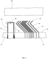
- Fig. 3 shows an alternative embodiment where the thermal detector is provided with a projection.
- the projection 40 extends the length of the thermal detector so that the distal end of the thermal detector (which now corresponds to the distal end of the projection 40) extends as far from the probe body 12 as the cantilevers, i.e. the distal end of the thermal detector is aligned with the distal end of the cantilevers. In this way, the thermal detector will contact the test sample substantially simultaneously with the cantilevers - depending on whether or not the probe is tilted to a certain degree.
- the thermal detector may then alternatively be used as a strain gauge in order to determine the distance between the probe and the test sample.
- the projection allows the thermal detector to be used as a contact probe, i.e. the thermal detector may have a dual or triple purpose.
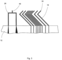
- Fig. 4 shows an alternative embodiment of the probe.
- the probe comprises a second thermal detector 42 in addition to the first thermal detector 26 and the cantilevers such that a possible tilting of the probe may be identified, i.e. whether or not the tips (distal ends) of the cantilevers are parallel to a test sample surface. This reduces the risk of one of the outer cantilevers diving deeper into the test sample than desired.
- the cantilevers are between the first thermal detector and the second thermal detector.
- the second thermal detector supports a second electrical conductor the same way as the first thermal detector, as explained above, i.e. the second electrical conductor has an electrical resistance, which is temperature dependent, and it forms a loop with respect to a third contact pad on the probe body and a fourth contact pad on the probe body such that it may be used as an electrical resistance in an electrical circuit.
- the presence of the second thermal detector increases the number of contact pads on the probe body with two.
- the two thermal conductors are ideally made as similar as possible, i.e. with the same anchor points/distances, and linewidths.
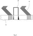
- Fig. 5 shows an alternative embodiment, where the cantilevers have been divided up and placed on opposite sides of a single thermal detector.
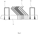
- Fig. 6 shows an alternative embodiment where a single cantilever is used.
- the single cantilever is constituted by an electrically insulating membrane 44 such as an oxide membrane.
- the single cantilever supports the first contact probe 24. Next to the first contact probe is shown seven other contact probes.
- the membrane 44 is shown supporting the electrical conductor 28 of the thermal detector, but it may be supported by a second membrane separate from the first membrane.
- the first contact probe extends with the respective distal end to the membrane edge 46, which is furthest from the probe body.
- the other contact probes also extend to the membrane edge.
- the distal end of the thermal detector 26 has a distance to the membrane edge 46, but it may extend all the way to the membrane edge.
- the membrane allows for the contact probes to be deposited with a smaller linewidth, i.e. the cantilevers can be closer together without breaking due to the otherwise narrow cantilever width for each individual contact probe.
- the distance between the tips of the contact probes along the first edge may be less than 1 ⁇ m.
- the electrical conductor 28 on the membrane 44 is shown as a loop with respect to the probe body 12.
- Fig. 7 shows an alternative embodiment of the probe.
- the membrane 44 is supported by a cantilever 18.
- a total of eight cantilevers may be used to support the membrane as illustrated in fig. 7 .
- the cantilevers together with the membrane form a loop with respect to the probe body such that the structure is more flexible than the probe shown in fig. 6 , where the membrane is supported by the probe body.
- the first cantilever 18 supports a contact probe, which extends onto the membrane all the way to the membrane edge 46.
- the two middle cantilevers each supports metal films, which extend onto the membrane and are joined together on the membrane thereby forming an electrical conductor 28, which forms a loop with respect to the probe body.
- the electrical conductor 28 may have a temperature dependent electrical resistance, which may be used as a thermal detector the same way as described above with respect to figs. 1-6 .
- the metal films are adjoined on the membrane a distance from the membrane edge. From the adjoining point may extend a projection 40 to the membrane edge parallel with the contact probe 24, i.e. the electrical conductor 28 includes a projection 40.
- the projection 40 may serve the function of a strain gauge, which may also be used to determine the distance between the probe and the test sample.
- the electrical conductor 28 may be used as a contact probe together with the other contact probes, i.e. the electrical conductor has a triple purpose as also described in connection with fig. 3 .
- the contact probes may be placed close together.
- the probe in fig. 7 has a total of seven contact probes which extend parallel and closely together on the membrane (closer than when the contact probes are supported by individual cantilevers).
- Fig. 8 shows a measurement with five probes.
- Each probe corresponds to one of the probes described in connection with any of figs. 2-7 such as the probe described in connection with fig. 2 .
- the measurement routine is performed also as described above in connection with fig. 2 .
- the five probes differ with respect to manufacturing tolerances, i.e. the anchor position (the anchor distance ⁇ to the probe body from the distal end of the thermal detector), and the linewidth ⁇ of the electrical conductor at the distal end of the thermal detector, and the thickness of the electrical conductor 28 are different from probe to probe (a probe has dimensions in the micro meter range, which means that it is difficult to manufacture each probe with the exact same anchor distance and linewidth).
- Probes 1, 2 and 3 have thermal detectors with electrical conductors 28, which are made of Ni with a thickness of 90 nm.
- Probes 4 and 5 have thermal detectors with electrical conductors 28, which are made of Ni with a thickness of 110 nm.
- each graph shows the measured electrical resistance as a function of the distance to the test sample. As the probe approaches the test sample, the electrical resistance decreases.
- the five graphs are offset from each other due to varying geometric dimensions of the five probes. Furthermore, the sensitivity of each probe is different, which is illustrated with tangents with different inclinations (tangents are shown in fig. 8 proximate a distance of 0 m for probes 3 and 5).
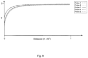
- Fig. 9 shows the results of a normalization of each of the measurements shown in fig. 8 .
- normalization and “rescaling” are used interchangeably.
- the graphs in fig. 9 have smaller offsets and smaller differences in tangents.
- the measured electrical resistance R(T), denoted ⁇ in fig. 8 is normalized with respect to geometric dimensions of the detector geometry, i.e. the anchor distance and the linewidth.
- the measured electrical resistance may be normalized with only one parameter.
- the offset between the graphs in fig. 8 is a function of the linewidth and metal (in this case Ni) film thickness, and the sensitivity is a function of the anchor distance, linewidth and metal film thickness.
- the linewidth of a thermal detector of a respective probe may be measured as the physical dimension in meters.
- the linewidth may be expressed in terms of the electrical resistance measured at room temperature with a current sufficiently low to not alter the temperature of the thermal detector in a measurable way (the voltage drop over the electrical conductor at room temperature, which takes on a value V 0 ).
- the anchor distance of a thermal detector of a respective probe may also be measured as the physical dimension in meters.
- the anchor distance may be expressed in terms of the difference between the electrical resistance measured at room temperature, and the electrical resistance measured at a temperature above room temperature (such as 5°C or 10°C above room temperature, depending on the current passing through the thermal detector).
- a first current having a first amplitude (such as 100 ⁇ A) is injected into the electrical conductor, and the corresponding electrical resistance of the electrical conductor is measured.
- a second current having a second amplitude (such as 1000 ⁇ A) is injected into the electrical conductor, and the corresponding electrical resistance of the electrical conductor is measured (the voltage drop over the electrical conductor at the higher temperature, which takes on a value V T ).
- the second current raises the temperature of the electrical conductor to a temperature above room temperature.
- the rescaled electrical resistance y 1 is a function of the measured electrical resistance, and the electrical resistance measured at room temperature, and the electrical resistance at a temperature above room temperature.
- the difference between the measured electrical resistance, R(T), and R' may be used to calculate a rescaled electrical resistance, where R' is the electrical resistance measured at a distance far enough away from the sample that the electrical resistance of the electrical conductor is unaffected by the proximity of the test sample.
- R' could be the electrical resistance measured at e.g. 100 ⁇ m, which is the measurement made furthest away from the sample.
- the above rescaled electrical resistance y is shown in fig. 9 and is a function of the difference between the measured electrical resistance, R(T), and R', and the electrical resistance measured at room temperature, and the electrical resistance at a temperature above room temperature.
- the rescaling brings the measurements closer together, i.e. the offset between the graphs in fig. 9 has become smaller, and the difference in sensitivity between the five probes is also smaller.
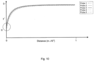
- Fig. 10 shows the results of a further rescaling of the measured electrical resistance of the electrical conductor.
- the graphs in fig. 10 have even smaller offsets and smaller differences in tangents.
- the measured electrical resistance is rescaled (multiplied) by the thickness ⁇ of the electrical conductor, i.e. the thickness of the metal film layer deposited on the thermal detector.
- the thickness may be known from the depositing process or it may be determined in an electrical measurement.
- the further rescaled electrical resistance y 1 ' is a function of the measured electrical resistance, and the electrical resistance measured at room temperature, and the electrical resistance at a temperature above room temperature, and the thickness of the electrical conductor.
- the further rescaled electrical resistance y' shown in fig. 10 is a function of the difference between the measured electrical resistance and R', and the electrical resistance measured at room temperature, and the electrical resistance at a temperature above room temperature, and the thickness of the electrical conductor.
- the normalization brings the measurements even closer together, i.e. the offset between the graphs in fig. 10 has become smaller, and the difference in sensitivity between the five probes is also smaller.
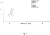
- Fig. 11 shows a magnification of the graphs in the circled area II of fig. 10 .
- the magnification shows that the normalization does not necessarily make the measurements with the five probes identical, and that the probes are stopped at different positions/distances to the test sample.
- the probes are stopped, there is a corresponding difference (error ⁇ ) between the probe, which is stopped with the contact probe closest to the test sample (probe 1), and the probe, which is stopped with the contact probe furthest to the test sample (probe 5).
- error ⁇ the difference between the probe, which is stopped with the contact probe closest to the test sample (probe 1), and the probe, which is stopped with the contact probe furthest to the test sample (probe 5).
- ⁇ - 1.600
- a number of measurements with a number of probes may be performed in order to determine, which threshold brings the error ⁇ below a certain (second) threshold. Since it is not desirable to have the probe go too deep into the test sample, a certain error may be accepted (such as 200 nm).
- the threshold ⁇ which is decisive for when the probe is stopped may be determined as a function of the error ⁇ - for example from an empirical experiment with five probes as described above, i.e. when the error ⁇ is below a value (such as 200 nm or 100 nm or 50 nm), the electrical resistance of the electrical conductor, which is measured when the error goes below that value, may be used as the threshold for when the probe is to be stopped in an actual measurement of a test sample to be measured.
- thermal detectors When a rescaling has been done, it may be used with all thermal detectors having the same design, i.e. same geometry, same dimensions, such as anchor distance and linewidth within manufacturing tolerances, and same materials.
- the thermal detector When the thermal detector has a projection, the geometry of the projection must also be the same (within manufacturing tolerances).
- thermal signal is the measured resistance of the electrical conductor, R(T), where an example is shown in fig. 8 .
- the calibration allows knowing the distance to the surface of a test sample at any given thermal signal measured for all the thermal detectors with that design.
- the electrical resistance of the electrical conductor 28 is measured using an alternating current injected in the electrical conductor, i.e. the current may be a sine wave with a certain phase with a fundamental frequency (1 st harmonic) selected in the range 1 Hz - 10 kHz such as 1 kHz.
- the current may be used to heat the electrical conductor or other means may be used to establish a temperature difference between the electrical conductor and the test sample as described above.
- the electrical resistance of the electrical conductor is then measured using an electronic circuit such as a Wheatstone bridge or a voltmeter.
- the measured electrical resistance is then filtered by means of a high pass filter with a cut off frequency lower than a second harmonic of the first frequency, i.e. for suppressing the first harmonic with respect to the higher harmonics.
- the measured electrical resistance can be filtered with a bandpass filter center around a specific higher order harmonic (such as the 2 nd harmonic) so that the selected harmonic component may be amplified with respect to the first harmonic.
- the filtered signal may then be used as a measure for the proximity between the thermal detector and the test sample.
- a threshold value may be determined empirically as described above.
Landscapes
- Physics & Mathematics (AREA)
- General Physics & Mathematics (AREA)
- Engineering & Computer Science (AREA)
- Environmental & Geological Engineering (AREA)
- Computer Hardware Design (AREA)
- General Engineering & Computer Science (AREA)
- Microelectronics & Electronic Packaging (AREA)
- Health & Medical Sciences (AREA)
- Toxicology (AREA)
- Mathematical Physics (AREA)
- Measurement Of Resistance Or Impedance (AREA)
- Measuring Leads Or Probes (AREA)
- Investigating Or Analyzing Materials Using Thermal Means (AREA)
- Testing Or Measuring Of Semiconductors Or The Like (AREA)
- Measurement Of Length, Angles, Or The Like Using Electric Or Magnetic Means (AREA)
Description
- The present invention relates to a method of contacting a probe with a test sample for testing an electrical property of the test sample, specifically the present invention is directed to a micro cantilever multi point probe with a thermal detector. The present invention furthermore relates to a system for testing an electrical property of a test sample, a method for rescaling a measurement of a thermal detector to compensate for geometrical variations, and a method of determining a proximity between a thermal detector and a test sample.
- A test sample may also consist of a semiconductor wafer with on top a thin planar continuous conducting film or a thin multilayer stack forming, for example a magnetic tunnelling junction (MTJ).
- The test sample may also be a semiconductor wafer of silicon having an integrated CMOS circuit implemented for example with a number of CMOS transistors. In this case, the sample may contain specific test pads where a portion of the conductive films or stack undertest is dedicated for electrical characterization. The test pads may also be composed by a dense array of finFET transistors.
- A multipoint probe measurement and test routine such as a four point probe measurement is also known as four terminal sensing, wherein an electrical impedance measuring technique uses separate pairs of current-carrying and voltage-sensing electrodes (contact probes with tips for contacting the test sample).
- When performing resistance measurements for determining electrical properties of a test sample, a test probe comprising one or more electrodes for establishing electrical contact to the test surface is brought into contact with the test surface.
-
- The probe is part of a test apparatus or system, which comprises an actuator for moving the probe into contact with the test sample, which is placed in the test apparatus.
- The dimensions are in the micro- or nanometer scale, and it is important to have a controlled and precise landing of the tip (tip end of the contact probe) on the test sample such that when the actuator stops, the tip is within at least 200 nm of the surface of the test sample and preferably within ± 50 nm of the surface of the test sample.
- A controlled landing may prevent the electrodes to break, and the test sample being contaminated with probe debris, and that a good stable ohmic contact may be established.
- The landing of the probe may be controlled using a strain gauge detector (mechanical contact detection) or using an electrical contact detection by measuring the electrical impedance between multiple contact probes for example, i.e. when the impedance between multiple contact probes decreases it may be assumed that the contact probes are in contact with the test sample and a current flows in the test sample between at least two contact probes.
- Each of these methods of landing or contacting the test sample have disadvantages such as a relative large total footprint, as in the case of strain gauge based surface detection, which requires an extra cantilever to touch the sample surface, with respect to the electrical detection. A larger footprint implies higher contamination of the sample from the contact with the probe. On the other hand, for non-conducting surfaces (or oxidized surfaces) of the test sample, the electrical detection does not work, limiting its applicability.
- An example of using heat to measure a distance across an air gap is disclosed in
US7186019 , which is incorporated in the present disclosure by reference. However, the device inUS7186019 has no contact probes for measuring an electrical property of the test sample, and the device is also not brought in contact with the test sample. -
US2009/261849 discloses a probe test card assembly for testing of a device under test.EP1045253 describes a probe for measuring electrical characteristics of a semiconductor device. - It is an object of the present invention to reduce at least some of the above mentioned disadvantages.
- The above object and advantages together with numerous other objects and advantages, which will be evident from the description of the present invention, are according to a first aspect of the present invention obtained by:
A method of approaching a probe to a test sample for testing an electrical property of said test sample as recited inclaim 1. - Proximate is to be understood as being near or so near that the contact probe abuts the test sample.
- The threshold value may be selected from empirical measurements such that the probe is stopped when it has a distance between 0-10 µm to the surface of the test sample.
- The probe may then be moved a fixed distance towards the test sample in order to bring the probe into physical contact with the test sample. This fixed distance may be selected from any of the ranges 0.5-8 µm, or 0.5-6 µm, or 0.5-4 µm, or 0.5-2 µm, or 1-7 µm, or 1-3 µm - depending on how far from the test sample the probe is stopped.
- Alternatively, the threshold value may be selected so that the probe contacts the test sample when the threshold value is reached. In such a case it is not necessary to move the probe the final distance in order to contact the test sample.
- Normally, the occurrence of a contact means that the probe has landed on the test sample with the tip of the contact probe contacting the surface of the test sample.
- However, in general, contacting is to be understood in the sense that the contact probe is not necessarily in physical contact with test sample, but that it is so close to the test sample that there exist a capacitive connection between the contact probe and the test sample such that an alternating current in the contact probe may run over into the test sample, i.e. the capacitive contact being greater than 0 and less than 1 mF.
- The probe may have a second cantilever extending from said probe body in a co-planar relationship with respect to the planar surface. The probe may also have a second thermal detector extending from said probe body in a co-planar relationship with respect to the planar surface.
- The temperature dependent electrical resistance may implicitly be measured by measuring the voltage drop across the temperature dependent electrical resistance.
- The first thermal detector may define a loop with respect to the probe body, i.e. the first thermal detector extends away from the probe body at a first point and returns to the probe body at a second point (the thermal detector begins and ends on the probe body).
- The temperature difference may be established by providing a heater, which heats the electrical conductor relative to the test sample, i.e. the temperature of the electrical conductor is increased more than the temperature of the test sample. The reverse may also be the case, i.e. a heater is provided, which heats the test sample relative to the electrical conductor.
- Alternatively, a cooler may be provided which cools the electrical conductor relative to the test sample - or the cooler may cool the test sample relative to the electrical conductor.
- The current injected in the electrical conductor may be used to heat the electrical conductor, i.e. the current may have an amplitude such that the electrical conductor is heated to a temperature above room temperature. The current may be an alternating current.
- The current may be injected in the electrical conductor by means of a current source, which may provide for a constant current being conducted in the electrical conductor.
- The first threshold value may be selected such that the distance between the contact probe and the test sample is below a second threshold value.
- The first threshold value may be selected such that the it is a function of a statistical distribution defining a variance between measurements with a plurality of probes - each probe being made according to the present invention.
- According to a second aspect of the present invention, the above objects and advantages are obtained by:
A system for testing an electrical property of a test sample as recited in claim 7. - The invention will now be explained in more detail below by means of examples of embodiments with reference to the very schematic drawing, in which
-
Fig. 1 shows a perspective of a probe for testing an electrical property of a test sample. -
Fig. 2 shows an enlarged view of section I infig. 1 . -
Fig. 3 shows an alternative embodiment where the thermal detector is provided with a projection. -
Fig. 4 shows an alternative embodiment of the probe. -
Fig. 5 shows an alternative embodiment, where the cantilevers have been divided up and placed on opposite sides of a single thermal detector. -
Fig. 6 shows an alternative embodiment where a single cantilever is used. -
Fig. 7 shows an alternative embodiment of the probe. -
Fig. 8 shows a measurement with five probes. -
Fig. 9 shows the results of a normalization of each of the measurements shown infig. 8 . -
Fig. 10 shows the results of a further rescaling of the measured electrical resistance of the electrical conductor. -
Fig. 11 shows a magnification of the graphs in the circled area II offig. 10 . - The present invention will now be described more fully hereinafter with reference to the accompanying drawings, in which exemplary embodiments of the invention are shown. The invention may, however, be embodied in different forms and should not be construed as limited to the embodiments set forth herein. Rather, these embodiments are provided so that this disclosure will be thorough and complete, and will fully convey the scope of the invention to those skilled in the art. Like reference numerals refer to like elements throughout. Like elements will, thus, not be described in detail with respect to the description of each figure.
-
Fig. 1 shows a perspective of a probe for testing an electrical property of a test sample. - The
probe 10 comprises aprobe body 12, which may be made of a number of semiconductor, metallic and/or dielectric layers. The probe body has a first side defining a substantial planar body surface, i.e. the surface is as planar as allowed by the manufacturing process. The probe body has a second side opposite the first side and a front side defining afront surface 32 between the first side and the second side. -
Fig. 2 shows an enlarged view of section I infig. 1 . - The
probe 10 comprises acantilever 18. Seven other cantilevers can be seen infig.2 , and the probe may in general have a set of cantilevers ranging from 1 to 16 cantilevers. - Each cantilever supports a
contact probe 24 for contacting a point or small area on the surface of the test sample, and establishes an electrical connection to the test sample. - It may be necessary to burn through an oxide layer on the test sample before measuring an electrical property of the test sample. This may be done with a current in the contact probe applied with a breakdown voltage (across two contact probes), which is high enough to cause a breakdown of the dielectric oxide - such voltage may be greater than 5 V.
- A contact probe or electrode is constituted by an electrically conducting metal film deposited on a cantilever surface facing the surface of the test sample when a test is performed. Normally, the metal film covers the width of the cantilever, since it is being deposited from above, and if no pattern is used to deposit the film, the film will cover what it lands on.
- The cantilevers are made of a dielectric material in order to electrically insulate the contact probe from the probe body such that a current does not run from one contact probe to another if the probe has a plurality of contact probes.
- The probe shown in
figs. 1 and2 is a micro eight point probe, but in general the probe may have any number of contact probes, i.e. the probe may have four contact probes thereby constituting a micro four point probe or it may have twelve contact probes thereby constituting a micro twelve point probe. - Each cantilever may support more than one contact probe.
- Each cantilever has an L-shape such that it is more flexible in three dimensions than a straight cantilever for example.
- Each cantilever has a distal end 30 (tip end comprising a tip) being furthest from the
probe body 12, i.e. with a certain distance between the distal end and the probe body. The distance between the distal end and the probe body is typically in the range of 5 to 200 µm. - A proximal end of a cantilever is defined as being opposite the distal end, i.e. furthest from the distal end. Thus, the proximal end being closer to the probe body than the distal end.
- Each cantilever is supported by the planar body surface at the proximal end and extends away from the probe body with a vector component in a direction normal to the
front surface 32 of theprobe body 12, and in a cantilever plane parallel to the planar surface of the probe body (co-planar with the planar body surface). When a cantilever contacts thetest sample 22 it may flex out of the cantilever plane. - The axis extending through the proximal end and the
distal end 30 constitutes a cantilever axis. Infig. 2 , the cantilever axis has an angle greater than zero with respect to the normal to thefront surface 32 of the probe body (in part because of the L-shape of the cantilever). The cantilever may also be straight, in which case the cantilever is to extend with the cantilever axis being parallel with the normal to the front surface. - The probe comprises a first thermal detector, which can be seen to the left of the cantilevers, and extending parallel to the cantilevers.
- The thermal detector extends in a detector plane parallel to the planar surface (co-planar with the planar body surface).
- The thermal detector extends away from the same
front surface 32 as the cantilevers. Infig. 2 , the thermal detector extends parallel to the normal of thefront surface 32. However, the thermal detector may have an angle between ± 60° with respect to the normal of thefront surface 32 in the detector plane. - The thermal detector defines a loop with respect to the probe body, i.e. it begins on the probe body, and ends on the probe body.
- In
fig. 2 , the thermal detector is formed by three straight segments constituted by afirst arm 34, asecond arm 36, and afront segment 38. The two arms are orthogonal to thefront surface 32, and the front segment is parallel to the front surface. - A proximal end of the first arm is supported by the planar surface, and a proximal end of the second arm is supported by the planar surface. The
front segment 38 extends between the distal end of the first arm and the distal end of the second arm. - More than three segments may be used to form the loop, and in a first alternative, the loop may be ring-formed defining a geometry such as a circle or an ellipse (not extending a full 360°). In a second alternative, the thermal detector may be formed by a plate, which may be as wide and long as the area covered by the three straight segments.
- A distal end of the thermal detector (constituted by a detector end) has an anchor position with an anchor distance α to the
probe body 12. The anchor distance (length of the thermal detector) is shown as being smaller than the distance between the distal end of a cantilever and the probe body. - It is contemplated that the thermal detector may extend as far away from the probe body as the
cantilever 18, i.e. the length of the thermal detector is substantially the same as the length of the cantilever (substantially means that the length of the thermal detector does not deviate with more than 10 % from the length of the cantilever). - It is also contemplated that the thermal detector may have a length, which is greater than the length of the cantilever, i.e.
- The anchor distance α may be less than 200 µm such as less than 180 µm, 160 µm, 140 µm, 120 µm, or 100 µm down to less than 50 µm.
- The
front segment 38 is shown with a linewidth β, which may be in the range of 20 nm - 20 µm, such as 100 nm - 10 µm or 1 µm - 5 µm. All the segments of the thermal detector may have such a width range. - The thermal detector supports an
electrical conductor 28, which is constituted by an electrically conducting metal film deposited on the thermal detector surface. The metal film normally covers the width of the thermal detector, i.e. the width of the electrical conductor (such as on the front segment) may correspond to the linewidth β. - The metal film may be of the same material as the contact probe such as nickel, tantalum, aluminium, platinum, ruthenium, titanium, cobalt, iron, tungsten. The electrical conductor has an electrical resistance, which is temperature dependent.
- Each contact probe (metal film) is connected to respective electrical lines on the
probe body 12. The electrical lines connect the contact probes with contact pads, i.e. thecontact probe 24 on thefirst cantilever 18 is electrically connected to a firstelectrical line 16, which leads to a first contact pad 14 (the contact probe and the electrical line may be deposited as a continuous metal film leading from the contact pad to the distal end of the cantilever). - Similarly, the
electrical conductor 28 may be formed by depositing a metal film leading from a first contact pad on the probe body onto the thermal detector, and back to a second contact pad, i.e. the electrical conductor may form a loop with respect to a first contact pad on the probe body and a second contact pad on the probe body such that it may be used as an electrical resistance in an electrical circuit with two terminals connected to the first and second contact pad. - The contact pads are for establishing electrical connections between the probe and a test apparatus, i.e. the test apparatus has terminals which engage the contact pads on the probe when the probe is placed in the test apparatus. The test apparatus also has a power source such as a current source or a voltage source, and one or more electronic circuits for sending signals on the contact probes and the electrical conductor of the thermal detector. The electronic circuits may be implemented as one or more microprocessors.
- An actuator of the test apparatus holds and moves the probe with respect to the test sample, which is also placed in the test apparatus.
- During a measurement with the probe, an alternating current with a constant amplitude is injected into the
electrical conductor 28 by means of a current source connected to the electrical conductor, i.e. the current may be a sine wave with a certain phase with a fundamental frequency (1st harmonic) selected in therange 1 Hz - 10 kHz such as 1 kHz. Alternatively, the current may be a direct current. - Instead of a current source, a voltage source may be connected across the electrical conductor whereby a current will flow in the electrical conductor.
- The current is to heat the
electrical conductor 28 to a temperature above room temperature, which may be achieved with a current with an amplitude selected in therange 10 µA - 10000 µA, such as 2000 µA, i.e. the power delivered to the electrical resistance of the electrical conductor is dissipated as heat. - In the present context, room temperature refers to a temperature between 15°C - 30°C, such as 20°C - 30°C, or 20°C - 25°C or 25°C - 30°C.
- Alternatively, the test sample may be heated to a temperature higher than that of the electrical conductor.
- Near room temperature, the resistivity of metals typically increases as temperature is increased. If the temperature T does not vary too much, a linear approximation is typically used: R(T) = R 0(1 + c(T - T 0)), where c is the temperature coefficient of resistance, T0 is a fixed reference temperature (usually room temperature), and R0 is the resistance at temperature T0.
- The probe is then moved towards the test sample, which is initially at room temperature.
- The probe is moved towards the test sample with an angle with respect to the surface of the test sample, i.e. the probe may be moved with an angle of ± 90° with respect to the normal of the test sample surface. Alternatively, the probe may be moved with an angle of 45° ± 40° (such as 45° ± 30° or 45° ± 15°) with respect to the surface of the test sample, i.e. it is not moved along the test sample parallel to the surface of the test sample.
- As the probe approaches the test sample, the dissipation of the heat, generated by the electrical conductor, changes. When the thermal detector is far away from the sample surface, the heat is mainly dissipated into the probe body through thermal conduction along the thermal detector structure. The closer the thermal detector gets to the sample surface, the higher is the fraction of the generated heat that dissipates through the air into the sample itself. In this case, the sample can be considered a heat sink at constant temperature.
- It is contemplated that the temperature of the electrical conductor decreases as the probe approaches the test sample (the current injected in the electrical conductor or the voltage across the electrical conductor may be held constant). The decrease in temperature of the electrical conductor means a decrease in the electrical resistance of the electrical conductor.
- The electronic circuit of the test apparatus is used to measure the electrical resistance of the electrical conductor as the probe is moved towards the test sample. The electrical resistance may be measured using a Wheatstone bridge where the electrical resistance of the electrical conductor is one of the four electrical resistances used in the bridge.
- Alternatively, a voltmeter may be used to measure the voltage drop across the electrical conductor (when the current is held constant, the measure of the voltage is a measure of the electrical resistance).
- If a voltage source is used to have a constant voltage across the electrical conductor, a measured current in the electrical conductor is a measure of the electrical resistance of the
electrical conductor 28. - The measure of the electrical resistance (the output provided by the measuring circuit of the electronic circuit) is used as a measure of how close the probe is to the test sample, i.e. the measure may be compared to a threshold value τ. When the measure of the electrical resistance reaches a threshold value, the probe is stopped.
- Alternatively, the change of the measure of the electrical resistance or the change in voltage drop, which are equivalent measures, may be used as a measure of how close the probe is to the test sample.
- The threshold value is selected so that when the threshold value is reached, the contact probe is in proximity to the test sample such that it only has to be moved a fixed distance the rest of the way towards the test sample.
- Alternatively, the threshold value is selected so that when the threshold value is reached, the contact probe contacts the test sample
- An electric connection may be established between the contact probe and the test sample when the contact probe is in contact with the test sample.
- The distance between the thermal detector and the sample surface should be reproducible from landing to landing and from probe to probe within 300 nm but preferably within 50 nm.
- The threshold value may be determined via empirical measurements or by determining it as a function of the difference between the length of the thermal detector (anchor distance) and the length of the cantilever (the distance between the distal end and the proximal end of the cantilever).
- Alternatively, the test sample may be heated while the current in the electrical conductor is held at a value, which does not heat the electrical conductor as much as the test sample is heated, i.e. the current may be at 100 µA for example, or lower.
- As the probe is moved towards the test sample, the electrical conductor will be heated up by heat dissipated from the test sample, and the electrical resistance of the electrical conductor will go up. This may be measured with the electronic circuit and used as a measure of how close the thermal detector is to the test sample, i.e. the method is reverse to the method when the electrical conductor is heated.
- It is also contemplated that the test sample may be cooled to a temperature below room temperature, which also provides for a temperature difference between the thermal detector and the test sample.
-
Fig. 3 shows an alternative embodiment where the thermal detector is provided with a projection. - The
projection 40 extends the length of the thermal detector so that the distal end of the thermal detector (which now corresponds to the distal end of the projection 40) extends as far from theprobe body 12 as the cantilevers, i.e. the distal end of the thermal detector is aligned with the distal end of the cantilevers. In this way, the thermal detector will contact the test sample substantially simultaneously with the cantilevers - depending on whether or not the probe is tilted to a certain degree. The thermal detector may then alternatively be used as a strain gauge in order to determine the distance between the probe and the test sample. - Further alternatively, the projection allows the thermal detector to be used as a contact probe, i.e. the thermal detector may have a dual or triple purpose.
-
Fig. 4 shows an alternative embodiment of the probe. - The probe comprises a second
thermal detector 42 in addition to the firstthermal detector 26 and the cantilevers such that a possible tilting of the probe may be identified, i.e. whether or not the tips (distal ends) of the cantilevers are parallel to a test sample surface. This reduces the risk of one of the outer cantilevers diving deeper into the test sample than desired. - The cantilevers are between the first thermal detector and the second thermal detector.
- The second thermal detector supports a second electrical conductor the same way as the first thermal detector, as explained above, i.e. the second electrical conductor has an electrical resistance, which is temperature dependent, and it forms a loop with respect to a third contact pad on the probe body and a fourth contact pad on the probe body such that it may be used as an electrical resistance in an electrical circuit. The presence of the second thermal detector increases the number of contact pads on the probe body with two.
- The two thermal conductors are ideally made as similar as possible, i.e. with the same anchor points/distances, and linewidths.
-
Fig. 5 shows an alternative embodiment, where the cantilevers have been divided up and placed on opposite sides of a single thermal detector. -
Fig. 6 shows an alternative embodiment where a single cantilever is used. - The single cantilever is constituted by an electrically insulating
membrane 44 such as an oxide membrane. The single cantilever supports thefirst contact probe 24. Next to the first contact probe is shown seven other contact probes. Themembrane 44 is shown supporting theelectrical conductor 28 of the thermal detector, but it may be supported by a second membrane separate from the first membrane. - The first contact probe extends with the respective distal end to the
membrane edge 46, which is furthest from the probe body. The other contact probes also extend to the membrane edge. - The distal end of the
thermal detector 26 has a distance to themembrane edge 46, but it may extend all the way to the membrane edge. - The membrane allows for the contact probes to be deposited with a smaller linewidth, i.e. the cantilevers can be closer together without breaking due to the otherwise narrow cantilever width for each individual contact probe. The distance between the tips of the contact probes along the first edge may be less than 1 µm.
- The
electrical conductor 28 on themembrane 44 is shown as a loop with respect to theprobe body 12. -
Fig. 7 shows an alternative embodiment of the probe. - The
membrane 44 is supported by acantilever 18. A total of eight cantilevers may be used to support the membrane as illustrated infig. 7 . - The cantilevers together with the membrane form a loop with respect to the probe body such that the structure is more flexible than the probe shown in
fig. 6 , where the membrane is supported by the probe body. - The
first cantilever 18 supports a contact probe, which extends onto the membrane all the way to themembrane edge 46. - The two middle cantilevers each supports metal films, which extend onto the membrane and are joined together on the membrane thereby forming an
electrical conductor 28, which forms a loop with respect to the probe body. Theelectrical conductor 28 may have a temperature dependent electrical resistance, which may be used as a thermal detector the same way as described above with respect tofigs. 1-6 . - The metal films are adjoined on the membrane a distance from the membrane edge. From the adjoining point may extend a
projection 40 to the membrane edge parallel with thecontact probe 24, i.e. theelectrical conductor 28 includes aprojection 40. Theprojection 40 may serve the function of a strain gauge, which may also be used to determine the distance between the probe and the test sample. Additionally, theelectrical conductor 28 may be used as a contact probe together with the other contact probes, i.e. the electrical conductor has a triple purpose as also described in connection withfig. 3 . - Due to the
membrane 28, the contact probes may be placed close together. With theelectrical conductor 28 also serving as a contact probe, the probe infig. 7 has a total of seven contact probes which extend parallel and closely together on the membrane (closer than when the contact probes are supported by individual cantilevers). -
Fig. 8 shows a measurement with five probes. - Each probe corresponds to one of the probes described in connection with any of
figs. 2-7 such as the probe described in connection withfig. 2 . The measurement routine is performed also as described above in connection withfig. 2 . - The five probes differ with respect to manufacturing tolerances, i.e. the anchor position (the anchor distance α to the probe body from the distal end of the thermal detector), and the linewidth β of the electrical conductor at the distal end of the thermal detector, and the thickness of the
electrical conductor 28 are different from probe to probe (a probe has dimensions in the micro meter range, which means that it is difficult to manufacture each probe with the exact same anchor distance and linewidth). -
Probes electrical conductors 28, which are made of Ni with a thickness of 90 nm. -
Probes electrical conductors 28, which are made of Ni with a thickness of 110 nm. - In a measurement, the respective probe is moved towards the test sample while the electrical conductor of the thermal detector is heated with an electrical current. Each graph shows the measured electrical resistance as a function of the distance to the test sample. As the probe approaches the test sample, the electrical resistance decreases.
- The five graphs are offset from each other due to varying geometric dimensions of the five probes. Furthermore, the sensitivity of each probe is different, which is illustrated with tangents with different inclinations (tangents are shown in
fig. 8 proximate a distance of 0 m forprobes 3 and 5). -
Fig. 9 shows the results of a normalization of each of the measurements shown infig. 8 . In this description, the terms "normalization" and "rescaling" are used interchangeably. - Compared to the graphs in
fig. 8 , the graphs infig. 9 have smaller offsets and smaller differences in tangents. - In the normalization, the measured electrical resistance R(T), denoted Ω in
fig. 8 , is normalized with respect to geometric dimensions of the detector geometry, i.e. the anchor distance and the linewidth. The measured electrical resistance may be normalized with only one parameter. - The offset between the graphs in
fig. 8 is a function of the linewidth and metal (in this case Ni) film thickness, and the sensitivity is a function of the anchor distance, linewidth and metal film thickness. - The linewidth of a thermal detector of a respective probe may be measured as the physical dimension in meters. Alternatively, the linewidth may be expressed in terms of the electrical resistance measured at room temperature with a current sufficiently low to not alter the temperature of the thermal detector in a measurable way (the voltage drop over the electrical conductor at room temperature, which takes on a value V0).
- The anchor distance of a thermal detector of a respective probe may also be measured as the physical dimension in meters. Alternatively, the anchor distance may be expressed in terms of the difference between the electrical resistance measured at room temperature, and the electrical resistance measured at a temperature above room temperature (such as 5°C or 10°C above room temperature, depending on the current passing through the thermal detector).
- For example, in a first measurement, a first current having a first amplitude (such as 100 µA) is injected into the electrical conductor, and the corresponding electrical resistance of the electrical conductor is measured.
- In a second measurement, a second current having a second amplitude (such as 1000 µA) is injected into the electrical conductor, and the corresponding electrical resistance of the electrical conductor is measured (the voltage drop over the electrical conductor at the higher temperature, which takes on a value VT). The second current raises the temperature of the electrical conductor to a temperature above room temperature.
- The difference between the two measurements, which take on the value ΔV= V0-VT is then used to express the anchor distance.
- Using the measured values V0 and ΔV, the measure of the electrical resistance of the electrical conductor may be rescaled for example by dividing it with the square of each output:

- The rescaled electrical resistance y1 is a function of the measured electrical resistance, and the electrical resistance measured at room temperature, and the electrical resistance at a temperature above room temperature.
- Alternatively, the difference between the measured electrical resistance, R(T), and R' may be used to calculate a rescaled electrical resistance, where R' is the electrical resistance measured at a distance far enough away from the sample that the electrical resistance of the electrical conductor is unaffected by the proximity of the test sample. In
fig. 8 , R' could be the electrical resistance measured at e.g. 100 µm, which is the measurement made furthest away from the sample. - In this case:

- The above rescaled electrical resistance y is shown in
fig. 9 and is a function of the difference between the measured electrical resistance, R(T), and R', and the electrical resistance measured at room temperature, and the electrical resistance at a temperature above room temperature. - Compared to the graphs in
fig. 8 , the rescaling brings the measurements closer together, i.e. the offset between the graphs infig. 9 has become smaller, and the difference in sensitivity between the five probes is also smaller. -
Fig. 10 shows the results of a further rescaling of the measured electrical resistance of the electrical conductor. - Compared to the rescaled graphs in
fig. 9 , the graphs infig. 10 have even smaller offsets and smaller differences in tangents. - In the further rescaling, the measured electrical resistance is rescaled (multiplied) by the thickness ω of the electrical conductor, i.e. the thickness of the metal film layer deposited on the thermal detector. The thickness may be known from the depositing process or it may be determined in an electrical measurement.
- Using the thickness ω, the normalized electrical resistance y1 of the electrical conductor may be further rescaled for example by multiplying it with the square of the thickness:

- Thus, the further rescaled electrical resistance y1' is a function of the measured electrical resistance, and the electrical resistance measured at room temperature, and the electrical resistance at a temperature above room temperature, and the thickness of the electrical conductor.
- In another example of a further rescaling, the rescaled electrical resistance y is rescaled (multiplied) by the square of the thickness ω of the electrical conductor, i.e. the thickness of the metal film layer deposited on the thermal detector:

- Thus, the further rescaled electrical resistance y' shown in
fig. 10 is a function of the difference between the measured electrical resistance and R', and the electrical resistance measured at room temperature, and the electrical resistance at a temperature above room temperature, and the thickness of the electrical conductor. - Compared to the graphs in
fig. 9 , the normalization brings the measurements even closer together, i.e. the offset between the graphs infig. 10 has become smaller, and the difference in sensitivity between the five probes is also smaller. -
Fig. 11 shows a magnification of the graphs in the circled area II offig. 10 . - Each probe is stopped when it reaches a threshold value (selected in the range between -1.000 to -2.000, and in the present case having τ = -1.600).
- The magnification shows that the normalization does not necessarily make the measurements with the five probes identical, and that the probes are stopped at different positions/distances to the test sample. At whichever threshold, the probes are stopped, there is a corresponding difference (error ε) between the probe, which is stopped with the contact probe closest to the test sample (probe 1), and the probe, which is stopped with the contact probe furthest to the test sample (probe 5). At a threshold value τ = - 1.600, the difference is 200 nm.
- A number of measurements with a number of probes may be performed in order to determine, which threshold brings the error ε below a certain (second) threshold. Since it is not desirable to have the probe go too deep into the test sample, a certain error may be accepted (such as 200 nm).
- Thus, the threshold τ which is decisive for when the probe is stopped may be determined as a function of the error ε - for example from an empirical experiment with five probes as described above, i.e. when the error ε is below a value (such as 200 nm or 100 nm or 50 nm), the electrical resistance of the electrical conductor, which is measured when the error goes below that value, may be used as the threshold for when the probe is to be stopped in an actual measurement of a test sample to be measured. In the empirical experiment shown in
fig. 11 , the determined threshold is τ = -1.600 as described above. - When a rescaling has been done, it may be used with all thermal detectors having the same design, i.e. same geometry, same dimensions, such as anchor distance and linewidth within manufacturing tolerances, and same materials. When the thermal detector has a projection, the geometry of the projection must also be the same (within manufacturing tolerances).
- If a thermal detector has been calibrated, i.e. a distance vs. thermal signal has been measured, all the other thermal detectors of the same design are calibrated thanks to the rescaling. The thermal signal is the measured resistance of the electrical conductor, R(T), where an example is shown in
fig. 8 . - Thus, of significance, the calibration allows knowing the distance to the surface of a test sample at any given thermal signal measured for all the thermal detectors with that design.
- As an alternative measurement procedure for the temperature dependent component of the electrical resistance of the electrical conductor, a high harmonic filtering is proposed.
- In such a method, the electrical resistance of the
electrical conductor 28 is measured using an alternating current injected in the electrical conductor, i.e. the current may be a sine wave with a certain phase with a fundamental frequency (1st harmonic) selected in therange 1 Hz - 10 kHz such as 1 kHz. - The current may be used to heat the electrical conductor or other means may be used to establish a temperature difference between the electrical conductor and the test sample as described above.
- The electrical resistance of the electrical conductor is then measured using an electronic circuit such as a Wheatstone bridge or a voltmeter.
- The measured electrical resistance is then filtered by means of a high pass filter with a cut off frequency lower than a second harmonic of the first frequency, i.e. for suppressing the first harmonic with respect to the higher harmonics. Alternatively, the measured electrical resistance can be filtered with a bandpass filter center around a specific higher order harmonic (such as the 2nd harmonic) so that the selected harmonic component may be amplified with respect to the first harmonic.
- The filtered signal may then be used as a measure for the proximity between the thermal detector and the test sample. Thus, when moving the probe towards the test sample the probe is stopped when the filtered signal reaches a threshold value. Such a threshold value may be determined empirically as described above.
- In the following is given a list of reference signs that are used in the detailed description of the invention and the drawings referred to in the detailed description of the invention.
-
- α
- Anchor distance
- β
- Linewidth of a thermal detector
- ω
- Thickness of the electrical conductor, i.e. the metal film thickness
- 10
- Probe
- 12
- Probe body
- 14
- Contact pad
- 16
- Electrical line
- 18
- Cantilever
- 22
- Test sample
- 24
- Contact probe
- 26
- Thermal detector
- 28
- Electrical conductor
- 30
- Distal end
- 32
- Front surface
- 34
- First arm
- 36
- Second arm
- 38
- Front segment
- 40
- Projection
- 42
- Second thermal detector
- 44
- Membrane
- 46
- Membrane edge
- 48
- Detector end
Claims (7)
- A method of approaching a probe (10) to a test sample for testing an electrical property of said test sample (22), said method comprising:providing a probe (10) having a probe body (12) defining a planar surface for supporting a first cantilever (18), a first thermal detector (26), and a second thermal detector (42),said first cantilever (18) extending from said probe body (12) in a co-planar relationship with respect to said planar surface between a first proximal end supported by said planar surface and a first distal end (30) opposite to said first proximal end,said first cantilever (18) having a cantilever surface supporting a first contact probe (24),said first thermal detector (26) extending from said probe body (12) in a co-planar relationship with respect to said planar surface between a second proximal end supported by said planar surface, and a second distal end opposite said second proximal end, said first thermal detector (26) having a detector surface supporting an electrical conductor (28) with a temperature dependent electrical resistance,said second thermal detector (42) extending from said probe body (12) in a co-planer relationship with respect to said planar surface between a third proximal end supported by said planar surface, and a third distal end opposite said third proximal end, said second thermal detector having a detector surface supporting an electrical conductor with a temperature dependent electrical resistance, said second thermal detector (42) being provided such that said first cantilever (18) is located between the first thermal detector (26) and the second thermal detector (42) on the planar surface,said method further comprising:establishing a temperature difference between said electrical conductor (28) and said test sample (22),injecting an electric current in said electrical conductor (28),providing an electronic circuit, connecting said electronic circuit to said electrical conductor (28), measuring said temperature dependent electrical resistance by means of said electronic circuit while moving said probe towards said test sample, andstopping said probe when said temperature dependent electrical resistance reaches a first threshold value representing the occurrence of said contact probe being in proximity or contacting said test sample.
- The method according to claim 1 , said probe having a second cantilever extending from said probe body (12) in a co-planar relationship with respect to said planar surface.
- The method according to any of the preceding claims, comprising measuring said temperature dependent electrical resistance by measuring said voltage drop across said temperature dependent electrical resistance.
- The method according to any of the preceding claims, said first thermal detector (26) defining a loop with respect to said probe body (12).
- The method according to any of the preceding claims, comprising providing a heater or a cooler for establishing said temperature difference between said electrical conductor and said test sample.
- The method according to any of the preceding claims, said current having an amplitude such that said electrical conductor (28) is heated to a temperature above room temperature.
- A system for testing an electrical property of a test sample (22), said system comprising: a probe (10) having a probe body (12) defining a planar surface for supporting a first cantilever (18), a first thermal detector (26), and a second thermal detector (42),said first cantilever (18) extending from said probe body (12) in a co-planar relationship with respect to said planar surface between a first proximal end supported by said planar surface and a first distal end opposite to said first proximal end,said first cantilever (18) having a cantilever surface supporting a first contact probe (24),said first thermal detector (26) extending from said probe body (12) in a co-planar relationship with respect to said planar surface between a second proximal end supported by said planar surface, and a second distal end opposite said second proximal end, said first thermal detector having a detector surface supporting an electrical conductor with a temperature dependent electrical resistance,said second thermal detector (42) extending from said probe body in a co-planer relationship with respect to said planar surface between a third proximal end supported by said planar surface, and a third distal end opposite said third proximal end, said second thermal detector having a detector surface supporting an electrical conductor with a temperature dependent electrical resistance, said second thermal detector being provided such that said first cantilever is located between the first thermal detector and the second thermal detector on the planar surface,said system further comprising:a heater or a cooler for establishing a temperature difference between said electrical conductor and said test sample,a power source interconnected with said electrical conductor for injecting a current in said temperature dependent electrical conductor,an actuator for moving said probe towards said test sample, and an electronic circuit interconnected with said electrical conductor for measuring said temperature dependent electrical resistance, and for comparing said temperature dependent electrical resistance with a threshold value.
Applications Claiming Priority (2)
| Application Number | Priority Date | Filing Date | Title |
|---|---|---|---|
| DKPA201700651 | 2017-11-15 | ||
| PCT/EP2018/080782 WO2019096695A2 (en) | 2017-11-15 | 2018-11-15 | A probe for testing an electrical property of a test sample |
Publications (2)
| Publication Number | Publication Date |
|---|---|
| EP3682253A2 EP3682253A2 (en) | 2020-07-22 |
| EP3682253B1 true EP3682253B1 (en) | 2024-11-13 |
Family
ID=64402171
Family Applications (1)
| Application Number | Title | Priority Date | Filing Date |
|---|---|---|---|
| EP18806994.2A Active EP3682253B1 (en) | 2017-11-15 | 2018-11-15 | A probe for testing an electrical property of a test sample and an associated proximity detector |
Country Status (6)
| Country | Link |
|---|---|
| US (1) | US11693028B2 (en) |
| EP (1) | EP3682253B1 (en) |
| JP (3) | JP7219276B2 (en) |
| KR (2) | KR102675691B1 (en) |
| CN (1) | CN111316110B (en) |
| WO (1) | WO2019096695A2 (en) |
Families Citing this family (6)
| Publication number | Priority date | Publication date | Assignee | Title |
|---|---|---|---|---|
| CN113494968B (en) * | 2020-03-19 | 2022-11-25 | 长鑫存储技术有限公司 | Temperature measurement and temperature calibration method and temperature measurement system |
| US11946890B2 (en) * | 2021-05-24 | 2024-04-02 | Kla Corporation | Method for measuring high resistivity test samples using voltages or resistances of spacings between contact probes |
| US12105136B2 (en) * | 2021-09-09 | 2024-10-01 | Kla Corporation | Method for determining material parameters of a multilayer test sample |
| JP7507838B2 (en) | 2021-11-30 | 2024-06-28 | イノヴェータム・インストゥルメンツ・インコーポレイテッド | Identifying XY location of a probe tip using a charged particle beam - Patents.com |
| US12306241B2 (en) | 2022-02-14 | 2025-05-20 | Innovatum Instruments Inc. | Automated probe landing |
| US12044727B2 (en) | 2022-09-19 | 2024-07-23 | Orbotech Ltd. | Probes for electrical testing in defect detection systems |
Family Cites Families (57)
| Publication number | Priority date | Publication date | Assignee | Title |
|---|---|---|---|---|
| US4201939A (en) * | 1978-06-26 | 1980-05-06 | Texas Instruments Incorporated | Multiprobe contact monitor and control system |
| JP2879282B2 (en) * | 1992-09-11 | 1999-04-05 | 東京エレクトロン株式会社 | Probe device |
| US5373231A (en) * | 1993-06-10 | 1994-12-13 | G. G. B. Industries, Inc. | Integrated circuit probing apparatus including a capacitor bypass structure |
| US5441343A (en) * | 1993-09-27 | 1995-08-15 | Topometrix Corporation | Thermal sensing scanning probe microscope and method for measurement of thermal parameters of a specimen |
| AU1794295A (en) * | 1994-05-13 | 1995-11-23 | Matsushita Electric Industrial Co., Ltd. | Radiation detector |
| US5561377A (en) * | 1995-04-14 | 1996-10-01 | Cascade Microtech, Inc. | System for evaluating probing networks |
| US6095679A (en) | 1996-04-22 | 2000-08-01 | Ta Instruments | Method and apparatus for performing localized thermal analysis and sub-surface imaging by scanning thermal microscopy |
| JPH11248723A (en) * | 1998-02-27 | 1999-09-17 | Nikon Corp | Atomic force microscope and approach to probe in it |
| JP4685240B2 (en) * | 1998-07-08 | 2011-05-18 | カプレス エイピーエス | Multi-probe probe |
| JP3735701B2 (en) | 1999-03-31 | 2006-01-18 | 独立行政法人産業技術総合研究所 | Electrical measurement prober and method of measuring electrical characteristics using the prober |
| JP2000356644A (en) * | 1999-06-15 | 2000-12-26 | Seiko Instruments Inc | Approach method and cantilever in scanning probe microscope apparatus using heat exchange effect |
| JP4526626B2 (en) * | 1999-12-20 | 2010-08-18 | 独立行政法人科学技術振興機構 | Electrical property evaluation equipment |
| TW550622B (en) | 2000-11-03 | 2003-09-01 | Ibm | Data storage device and read/write component for data storage device |
| EP1466182B1 (en) * | 2002-01-07 | 2011-08-03 | Capres A/S | Electrical feedback detection system for multi-point probes |
| KR100465235B1 (en) | 2002-04-16 | 2005-01-13 | 삼성전자주식회사 | RF power sensor capable of sensing power of RF signal using capacitance |
| AU2003253213A1 (en) | 2002-08-29 | 2004-03-19 | International Business Machines Corporation | Thermal movement sensor |
| JP2004093352A (en) * | 2002-08-30 | 2004-03-25 | Seiko Instruments Inc | Method for manufacturing ultra-fine multi-probe probe and surface characteristic analyzer |
| US7448798B1 (en) * | 2003-06-18 | 2008-11-11 | Veeco Instruments Inc. | Scanning thermal probe microscope |
| KR20060043141A (en) * | 2004-02-23 | 2006-05-15 | 지벡스 코포레이션 | Charged particle beam device probe manipulator |
| TWI372868B (en) * | 2005-01-13 | 2012-09-21 | Ibm | Probe for scanning over a substrate and data storage device |
| US7497613B2 (en) | 2005-04-18 | 2009-03-03 | Anasys Instruments | Probe with embedded heater for nanoscale analysis |
| US7706109B2 (en) * | 2005-10-18 | 2010-04-27 | Seagate Technology Llc | Low thermal coefficient of resistivity on-slider tunneling magneto-resistive shunt resistor |
| CN100507577C (en) * | 2005-10-24 | 2009-07-01 | 旺矽科技股份有限公司 | Probe Unit for Probe Cards |
| EP1780550A1 (en) * | 2005-10-31 | 2007-05-02 | Capres A/S | A probe for testing electrical properties of test samples |
| JP4936788B2 (en) | 2006-05-16 | 2012-05-23 | 株式会社東京精密 | Prober and probe contact method |
| EP1970714A1 (en) * | 2007-03-12 | 2008-09-17 | Capres Aps | Device including a contact detector |
| DE102007031112A1 (en) | 2007-06-27 | 2009-01-02 | Technische Universität Ilmenau | Apparatus and method for investigating surface properties of various materials |
| EP2198316A1 (en) * | 2007-09-03 | 2010-06-23 | Capres A/S | A method of determining an electrical property of a test sample |
| US7928343B2 (en) * | 2007-12-04 | 2011-04-19 | The Board Of Trustees Of The University Of Illinois | Microcantilever heater-thermometer with integrated temperature-compensated strain sensor |
| CN201145934Y (en) * | 2007-12-11 | 2008-11-05 | 青岛中阳消防科技有限公司 | Linear constant temperature fire detector capable of ranging |
| WO2009097487A1 (en) * | 2008-01-31 | 2009-08-06 | The Board Of Trustees Of The University Of Illinois | Temperature-dependent nanoscale contact potential measurement technique and device |
| US7733104B2 (en) * | 2008-04-21 | 2010-06-08 | Sv Probe Pte. Ltd. | Low force interconnects for probe cards |
| EP2141503A1 (en) * | 2008-06-30 | 2010-01-06 | Capres A/S | A multi-point probe for testing electrical properties and a method of producing a multi-point probe |
| US8931950B2 (en) * | 2008-08-20 | 2015-01-13 | The Board Of Trustees Of The University Of Illinois | Device for calorimetric measurement |
| WO2010044438A1 (en) | 2008-10-15 | 2010-04-22 | 株式会社村田製作所 | Heat sensor, non-contact temperature measuring device, and non-contact temperature measuring method |
| US20100116038A1 (en) * | 2008-11-12 | 2010-05-13 | International Business Machines Corporation | Feedback- enhanced thermo-electric topography sensing |
| US8441272B2 (en) * | 2008-12-30 | 2013-05-14 | Stmicroelectronics S.R.L. | MEMS probe for probe cards for integrated circuits |
| KR101001670B1 (en) * | 2009-02-23 | 2010-12-15 | 양 전자시스템 주식회사 | Probe Device for Flat Panel Display Inspection |
| US8297113B2 (en) * | 2009-03-16 | 2012-10-30 | Seagate Technology Llc | Media certification device design |
| US8393785B2 (en) * | 2009-05-14 | 2013-03-12 | Palo Alto Research Center Incorporated | Nanocalorimeter based on thermal probes |
| JP5461917B2 (en) * | 2009-08-12 | 2014-04-02 | 株式会社日立ハイテクサイエンス | Softening point measuring device and heat conduction measuring device |
| JPWO2011024303A1 (en) * | 2009-08-31 | 2013-01-24 | 株式会社アドバンテスト | Probe, probe card and electronic component testing apparatus |
| JP2011198243A (en) * | 2010-03-23 | 2011-10-06 | Micronics Japan Co Ltd | Device, method and program for adjusting relative parallelism of probe unit, probe unit and panel conveyance member |
| US8297837B1 (en) * | 2010-04-01 | 2012-10-30 | Angelo Gaitas | Metal and semimetal sensors near the metal insulator transition regime |
| TWI412750B (en) * | 2011-04-01 | 2013-10-21 | Chroma Ate Inc | Probe circuit |
| GB2493585B (en) * | 2011-08-11 | 2013-08-14 | Ibm | Scanning probe microscopy cantilever comprising an electromagnetic sensor |
| US8533861B2 (en) | 2011-08-15 | 2013-09-10 | The Board Of Trustees Of The University Of Illinois | Magnetic actuation and thermal cantilevers for temperature and frequency dependent atomic force microscopy |
| US9039280B2 (en) * | 2012-01-20 | 2015-05-26 | Purdue Research Foundation | Highly-reliable micro-electromechanical system temperature sensor |
| US8643444B2 (en) * | 2012-06-04 | 2014-02-04 | Broadcom Corporation | Common reference crystal systems |
| KR20140006289A (en) * | 2012-07-02 | 2014-01-16 | 한국표준과학연구원 | Apparatus for measuring thermoelectric properties of nano material, method for measuring thermoelectric properties of nano material and method of manufacturing the same |
| US9082440B2 (en) | 2012-07-23 | 2015-07-14 | Seagate Technology Llc | Using first and second resistive sensor bias levels to detect head-to-disk contact and/or clearance |
| JP6089725B2 (en) | 2013-01-28 | 2017-03-08 | 株式会社デンソー | Battery monitoring device |
| US9202499B2 (en) | 2013-03-13 | 2015-12-01 | Seagate Technology Llc | Contact detection using laser modulation |
| US9714983B2 (en) * | 2014-07-24 | 2017-07-25 | Nucleus Scientific Inc. | Test instrument for testing charge storage devices |
| JP6280519B2 (en) * | 2015-05-01 | 2018-02-14 | 株式会社ヒットデバイス | Electronic component temperature characteristic evaluation apparatus and temperature control unit used therefor |
| JP6418118B2 (en) * | 2015-09-24 | 2018-11-07 | 三菱電機株式会社 | Semiconductor device evaluation apparatus and evaluation method |
| JP2017166845A (en) | 2016-03-14 | 2017-09-21 | ジルコア インコーポレイテッド | Sensor tuning method to improve signal output stability for mixed gas measurement |
-
2018
- 2018-11-15 KR KR1020247013167A patent/KR102675691B1/en active Active
- 2018-11-15 KR KR1020207016406A patent/KR102660769B1/en active Active
- 2018-11-15 JP JP2020526477A patent/JP7219276B2/en active Active
- 2018-11-15 EP EP18806994.2A patent/EP3682253B1/en active Active
- 2018-11-15 CN CN201880071948.2A patent/CN111316110B/en active Active
- 2018-11-15 WO PCT/EP2018/080782 patent/WO2019096695A2/en not_active Ceased
- 2018-11-15 US US16/764,038 patent/US11693028B2/en active Active
-
2022
- 2022-12-12 JP JP2022197754A patent/JP7442609B2/en active Active
-
2024
- 2024-02-20 JP JP2024023415A patent/JP7607812B2/en active Active
Also Published As
| Publication number | Publication date |
|---|---|
| KR20240056786A (en) | 2024-04-30 |
| EP3682253A2 (en) | 2020-07-22 |
| JP2021503084A (en) | 2021-02-04 |
| KR102675691B1 (en) | 2024-06-14 |
| WO2019096695A2 (en) | 2019-05-23 |
| WO2019096695A3 (en) | 2019-06-20 |
| CN111316110B (en) | 2023-07-14 |
| KR102660769B1 (en) | 2024-04-24 |
| CN111316110A (en) | 2020-06-19 |
| JP7442609B2 (en) | 2024-03-04 |
| JP2024055910A (en) | 2024-04-19 |
| KR20200085316A (en) | 2020-07-14 |
| US11693028B2 (en) | 2023-07-04 |
| JP2023017085A (en) | 2023-02-02 |
| JP7607812B2 (en) | 2024-12-27 |
| JP7219276B2 (en) | 2023-02-07 |
| US20200278380A1 (en) | 2020-09-03 |
Similar Documents
| Publication | Publication Date | Title |
|---|---|---|
| US11693028B2 (en) | Probe for testing an electrical property of a test sample | |
| KR100978699B1 (en) | Electrical feedback detection system and multi point testing device | |
| US10495678B2 (en) | Testing method for sheet resistance and contact resistance of connecting point of sheet material | |
| JP2011526360A (en) | Multi-point probe for inspecting electrical characteristics and method of manufacturing multi-point probe | |
| Raven | Experimental measurements of the skin effect and internal inductance at low frequencies | |
| JPS62168043A (en) | Method and circuit for measuring semiconductor wafer by using four-point probe | |
| CN103582821B (en) | For contactless device, Electricity testing pliers and the method for determining the current potential of object | |
| US20110285416A1 (en) | Multi-point probe for testing electrical properties and a method of producing a multi-point probe | |
| CN115362355B (en) | Device for temperature measurement and device for current determination | |
| US3287637A (en) | High frequency current means including capacitive probe members for determining the electrical resistance of a semiconductor layer | |
| EP3994455A1 (en) | Systems and methods for measuring electrical characteristics of a material using a non-destructive multi-point probe | |
| US11340261B2 (en) | Flexible electric probe | |
| WO2003050552B1 (en) | Testing current perpendicular to plane giant magnetoresistance multilayer devices | |
| TWI892013B (en) | A method for measuring high resistivity test samples | |
| JP2001141766A (en) | Resistance measuring device and resistance measuring method | |
| RU2109276C1 (en) | Process of nondestructive test of surface layer of metal | |
| EP3683537A1 (en) | Displacement sensor | |
| Mbarek et al. | Near-field microwave CPW antenna for scanning microscopy | |
| US5469069A (en) | Method and apparatus for measuring resistivity of geometrically undefined materials | |
| EP2871487A1 (en) | Small scale measurements of anisotropic sheet conductances | |
| Enderling et al. | Quantitative analysis of Joule heating in surface micromachined Greek cross test structures | |
| PL242398B1 (en) | Method for determining sheet resistance | |
| Turner | Practical issues in the probing of copper pads. | |
| Gurrum et al. | A coaxial probe system for measuring Z-direction electrical resistivity of conductive polymers | |
| Maryniak et al. | Using a Concentric Ring Probe Technique |
Legal Events
| Date | Code | Title | Description |
|---|---|---|---|
| STAA | Information on the status of an ep patent application or granted ep patent |
Free format text: STATUS: UNKNOWN |
|
| STAA | Information on the status of an ep patent application or granted ep patent |
Free format text: STATUS: THE INTERNATIONAL PUBLICATION HAS BEEN MADE |
|
| PUAI | Public reference made under article 153(3) epc to a published international application that has entered the european phase |
Free format text: ORIGINAL CODE: 0009012 |
|
| STAA | Information on the status of an ep patent application or granted ep patent |
Free format text: STATUS: REQUEST FOR EXAMINATION WAS MADE |
|
| 17P | Request for examination filed |
Effective date: 20200414 |
|
| AK | Designated contracting states |
Kind code of ref document: A2 Designated state(s): AL AT BE BG CH CY CZ DE DK EE ES FI FR GB GR HR HU IE IS IT LI LT LU LV MC MK MT NL NO PL PT RO RS SE SI SK SM TR |
|
| AX | Request for extension of the european patent |
Extension state: BA ME |
|
| DAV | Request for validation of the european patent (deleted) | ||
| DAX | Request for extension of the european patent (deleted) | ||
| STAA | Information on the status of an ep patent application or granted ep patent |
Free format text: STATUS: EXAMINATION IS IN PROGRESS |
|
| 17Q | First examination report despatched |
Effective date: 20221206 |
|
| P01 | Opt-out of the competence of the unified patent court (upc) registered |
Effective date: 20230526 |
|
| GRAP | Despatch of communication of intention to grant a patent |
Free format text: ORIGINAL CODE: EPIDOSNIGR1 |
|
| STAA | Information on the status of an ep patent application or granted ep patent |
Free format text: STATUS: GRANT OF PATENT IS INTENDED |
|
| INTG | Intention to grant announced |
Effective date: 20240618 |
|
| GRAS | Grant fee paid |
Free format text: ORIGINAL CODE: EPIDOSNIGR3 |
|
| GRAA | (expected) grant |
Free format text: ORIGINAL CODE: 0009210 |
|
| STAA | Information on the status of an ep patent application or granted ep patent |
Free format text: STATUS: THE PATENT HAS BEEN GRANTED |
|
| AK | Designated contracting states |
Kind code of ref document: B1 Designated state(s): AL AT BE BG CH CY CZ DE DK EE ES FI FR GB GR HR HU IE IS IT LI LT LU LV MC MK MT NL NO PL PT RO RS SE SI SK SM TR |
|
| REG | Reference to a national code |
Ref country code: GB Ref legal event code: FG4D |
|
| REG | Reference to a national code |
Ref country code: CH Ref legal event code: EP |
|
| REG | Reference to a national code |
Ref country code: IE Ref legal event code: FG4D Ref country code: NL Ref legal event code: FP |
|
| REG | Reference to a national code |
Ref country code: DE Ref legal event code: R096 Ref document number: 602018076571 Country of ref document: DE |
|
| REG | Reference to a national code |
Ref country code: LT Ref legal event code: MG9D |
|
| PG25 | Lapsed in a contracting state [announced via postgrant information from national office to epo] |
Ref country code: IS Free format text: LAPSE BECAUSE OF FAILURE TO SUBMIT A TRANSLATION OF THE DESCRIPTION OR TO PAY THE FEE WITHIN THE PRESCRIBED TIME-LIMIT Effective date: 20250313 Ref country code: HR Free format text: LAPSE BECAUSE OF FAILURE TO SUBMIT A TRANSLATION OF THE DESCRIPTION OR TO PAY THE FEE WITHIN THE PRESCRIBED TIME-LIMIT Effective date: 20241113 Ref country code: PT Free format text: LAPSE BECAUSE OF FAILURE TO SUBMIT A TRANSLATION OF THE DESCRIPTION OR TO PAY THE FEE WITHIN THE PRESCRIBED TIME-LIMIT Effective date: 20250313 |
|
| PG25 | Lapsed in a contracting state [announced via postgrant information from national office to epo] |
Ref country code: FI Free format text: LAPSE BECAUSE OF FAILURE TO SUBMIT A TRANSLATION OF THE DESCRIPTION OR TO PAY THE FEE WITHIN THE PRESCRIBED TIME-LIMIT Effective date: 20241113 |
|
| REG | Reference to a national code |
Ref country code: AT Ref legal event code: MK05 Ref document number: 1742068 Country of ref document: AT Kind code of ref document: T Effective date: 20241113 |
|
| PG25 | Lapsed in a contracting state [announced via postgrant information from national office to epo] |
Ref country code: BG Free format text: LAPSE BECAUSE OF FAILURE TO SUBMIT A TRANSLATION OF THE DESCRIPTION OR TO PAY THE FEE WITHIN THE PRESCRIBED TIME-LIMIT Effective date: 20241113 |
|
| PG25 | Lapsed in a contracting state [announced via postgrant information from national office to epo] |
Ref country code: ES Free format text: LAPSE BECAUSE OF FAILURE TO SUBMIT A TRANSLATION OF THE DESCRIPTION OR TO PAY THE FEE WITHIN THE PRESCRIBED TIME-LIMIT Effective date: 20241113 |
|
| PG25 | Lapsed in a contracting state [announced via postgrant information from national office to epo] |
Ref country code: NO Free format text: LAPSE BECAUSE OF FAILURE TO SUBMIT A TRANSLATION OF THE DESCRIPTION OR TO PAY THE FEE WITHIN THE PRESCRIBED TIME-LIMIT Effective date: 20250213 |
|
| PG25 | Lapsed in a contracting state [announced via postgrant information from national office to epo] |
Ref country code: LV Free format text: LAPSE BECAUSE OF FAILURE TO SUBMIT A TRANSLATION OF THE DESCRIPTION OR TO PAY THE FEE WITHIN THE PRESCRIBED TIME-LIMIT Effective date: 20241113 Ref country code: AT Free format text: LAPSE BECAUSE OF FAILURE TO SUBMIT A TRANSLATION OF THE DESCRIPTION OR TO PAY THE FEE WITHIN THE PRESCRIBED TIME-LIMIT Effective date: 20241113 Ref country code: GR Free format text: LAPSE BECAUSE OF FAILURE TO SUBMIT A TRANSLATION OF THE DESCRIPTION OR TO PAY THE FEE WITHIN THE PRESCRIBED TIME-LIMIT Effective date: 20250214 |
|
| PG25 | Lapsed in a contracting state [announced via postgrant information from national office to epo] |
Ref country code: PL Free format text: LAPSE BECAUSE OF FAILURE TO SUBMIT A TRANSLATION OF THE DESCRIPTION OR TO PAY THE FEE WITHIN THE PRESCRIBED TIME-LIMIT Effective date: 20241113 |
|
| PG25 | Lapsed in a contracting state [announced via postgrant information from national office to epo] |
Ref country code: RS Free format text: LAPSE BECAUSE OF FAILURE TO SUBMIT A TRANSLATION OF THE DESCRIPTION OR TO PAY THE FEE WITHIN THE PRESCRIBED TIME-LIMIT Effective date: 20250213 |
|
| REG | Reference to a national code |
Ref country code: CH Ref legal event code: PL |
|
| PG25 | Lapsed in a contracting state [announced via postgrant information from national office to epo] |
Ref country code: SM Free format text: LAPSE BECAUSE OF FAILURE TO SUBMIT A TRANSLATION OF THE DESCRIPTION OR TO PAY THE FEE WITHIN THE PRESCRIBED TIME-LIMIT Effective date: 20241113 |
|
| PG25 | Lapsed in a contracting state [announced via postgrant information from national office to epo] |
Ref country code: DK Free format text: LAPSE BECAUSE OF FAILURE TO SUBMIT A TRANSLATION OF THE DESCRIPTION OR TO PAY THE FEE WITHIN THE PRESCRIBED TIME-LIMIT Effective date: 20241113 |
|
| PG25 | Lapsed in a contracting state [announced via postgrant information from national office to epo] |
Ref country code: LU Free format text: LAPSE BECAUSE OF NON-PAYMENT OF DUE FEES Effective date: 20241115 |
|
| REG | Reference to a national code |
Ref country code: CH Ref legal event code: PL |
|
| PG25 | Lapsed in a contracting state [announced via postgrant information from national office to epo] |
Ref country code: EE Free format text: LAPSE BECAUSE OF FAILURE TO SUBMIT A TRANSLATION OF THE DESCRIPTION OR TO PAY THE FEE WITHIN THE PRESCRIBED TIME-LIMIT Effective date: 20241113 |
|
| PG25 | Lapsed in a contracting state [announced via postgrant information from national office to epo] |
Ref country code: CH Free format text: LAPSE BECAUSE OF NON-PAYMENT OF DUE FEES Effective date: 20241130 |
|
| PG25 | Lapsed in a contracting state [announced via postgrant information from national office to epo] |
Ref country code: RO Free format text: LAPSE BECAUSE OF FAILURE TO SUBMIT A TRANSLATION OF THE DESCRIPTION OR TO PAY THE FEE WITHIN THE PRESCRIBED TIME-LIMIT Effective date: 20241113 |
|
| PG25 | Lapsed in a contracting state [announced via postgrant information from national office to epo] |
Ref country code: SK Free format text: LAPSE BECAUSE OF FAILURE TO SUBMIT A TRANSLATION OF THE DESCRIPTION OR TO PAY THE FEE WITHIN THE PRESCRIBED TIME-LIMIT Effective date: 20241113 |
|
| PG25 | Lapsed in a contracting state [announced via postgrant information from national office to epo] |
Ref country code: CZ Free format text: LAPSE BECAUSE OF FAILURE TO SUBMIT A TRANSLATION OF THE DESCRIPTION OR TO PAY THE FEE WITHIN THE PRESCRIBED TIME-LIMIT Effective date: 20241113 |
|
| PG25 | Lapsed in a contracting state [announced via postgrant information from national office to epo] |
Ref country code: IT Free format text: LAPSE BECAUSE OF FAILURE TO SUBMIT A TRANSLATION OF THE DESCRIPTION OR TO PAY THE FEE WITHIN THE PRESCRIBED TIME-LIMIT Effective date: 20241113 |
|
| REG | Reference to a national code |
Ref country code: DE Ref legal event code: R097 Ref document number: 602018076571 Country of ref document: DE |
|
| REG | Reference to a national code |
Ref country code: BE Ref legal event code: MM Effective date: 20241130 |
|
| PG25 | Lapsed in a contracting state [announced via postgrant information from national office to epo] |
Ref country code: SE Free format text: LAPSE BECAUSE OF FAILURE TO SUBMIT A TRANSLATION OF THE DESCRIPTION OR TO PAY THE FEE WITHIN THE PRESCRIBED TIME-LIMIT Effective date: 20241113 |
|
| PG25 | Lapsed in a contracting state [announced via postgrant information from national office to epo] |
Ref country code: MC Free format text: LAPSE BECAUSE OF FAILURE TO SUBMIT A TRANSLATION OF THE DESCRIPTION OR TO PAY THE FEE WITHIN THE PRESCRIBED TIME-LIMIT Effective date: 20241113 |
|
| PLBE | No opposition filed within time limit |
Free format text: ORIGINAL CODE: 0009261 |
|
| STAA | Information on the status of an ep patent application or granted ep patent |
Free format text: STATUS: NO OPPOSITION FILED WITHIN TIME LIMIT |
|
| PG25 | Lapsed in a contracting state [announced via postgrant information from national office to epo] |
Ref country code: BE Free format text: LAPSE BECAUSE OF NON-PAYMENT OF DUE FEES Effective date: 20241130 |
|
| 26N | No opposition filed |
Effective date: 20250814 |
|
| PG25 | Lapsed in a contracting state [announced via postgrant information from national office to epo] |
Ref country code: IE Free format text: LAPSE BECAUSE OF NON-PAYMENT OF DUE FEES Effective date: 20241115 |
|
| PGFP | Annual fee paid to national office [announced via postgrant information from national office to epo] |
Ref country code: NL Payment date: 20251126 Year of fee payment: 8 |
|
| PGFP | Annual fee paid to national office [announced via postgrant information from national office to epo] |
Ref country code: DE Payment date: 20251128 Year of fee payment: 8 |
|
| PGFP | Annual fee paid to national office [announced via postgrant information from national office to epo] |
Ref country code: GB Payment date: 20251127 Year of fee payment: 8 |
|
| PGFP | Annual fee paid to national office [announced via postgrant information from national office to epo] |
Ref country code: FR Payment date: 20251125 Year of fee payment: 8 |
|
| PG25 | Lapsed in a contracting state [announced via postgrant information from national office to epo] |
Ref country code: HU Free format text: LAPSE BECAUSE OF FAILURE TO SUBMIT A TRANSLATION OF THE DESCRIPTION OR TO PAY THE FEE WITHIN THE PRESCRIBED TIME-LIMIT; INVALID AB INITIO Effective date: 20181115 |
|
| PG25 | Lapsed in a contracting state [announced via postgrant information from national office to epo] |
Ref country code: CY Free format text: LAPSE BECAUSE OF FAILURE TO SUBMIT A TRANSLATION OF THE DESCRIPTION OR TO PAY THE FEE WITHIN THE PRESCRIBED TIME-LIMIT; INVALID AB INITIO Effective date: 20181115 |
|
| PG25 | Lapsed in a contracting state [announced via postgrant information from national office to epo] |
Ref country code: TR Free format text: LAPSE BECAUSE OF FAILURE TO SUBMIT A TRANSLATION OF THE DESCRIPTION OR TO PAY THE FEE WITHIN THE PRESCRIBED TIME-LIMIT Effective date: 20241113 |
|
| PG25 | Lapsed in a contracting state [announced via postgrant information from national office to epo] |
Ref country code: SI Free format text: LAPSE BECAUSE OF FAILURE TO SUBMIT A TRANSLATION OF THE DESCRIPTION OR TO PAY THE FEE WITHIN THE PRESCRIBED TIME-LIMIT Effective date: 20241113 |
|
| PG25 | Lapsed in a contracting state [announced via postgrant information from national office to epo] |
Ref country code: LT Free format text: LAPSE BECAUSE OF FAILURE TO SUBMIT A TRANSLATION OF THE DESCRIPTION OR TO PAY THE FEE WITHIN THE PRESCRIBED TIME-LIMIT Effective date: 20241113 |