EP3680940A1 - Semiconductor wafer manufacturing method, method of manufacturing semiconductor energy beam detecting element, and semiconductor wafer - Google Patents
Semiconductor wafer manufacturing method, method of manufacturing semiconductor energy beam detecting element, and semiconductor wafer Download PDFInfo
- Publication number
- EP3680940A1 EP3680940A1 EP18854988.5A EP18854988A EP3680940A1 EP 3680940 A1 EP3680940 A1 EP 3680940A1 EP 18854988 A EP18854988 A EP 18854988A EP 3680940 A1 EP3680940 A1 EP 3680940A1
- Authority
- EP
- European Patent Office
- Prior art keywords
- semiconductor region
- semiconductor
- main surface
- region
- cutting line
- Prior art date
- Legal status (The legal status is an assumption and is not a legal conclusion. Google has not performed a legal analysis and makes no representation as to the accuracy of the status listed.)
- Pending
Links
- 239000004065 semiconductor Substances 0.000 title claims abstract description 427
- 238000004519 manufacturing process Methods 0.000 title claims description 50
- 239000012535 impurity Substances 0.000 claims abstract description 71
- 229910052751 metal Inorganic materials 0.000 claims description 11
- 239000002184 metal Substances 0.000 claims description 11
- 238000005468 ion implantation Methods 0.000 claims description 9
- 238000005520 cutting process Methods 0.000 claims description 8
- 230000000149 penetrating effect Effects 0.000 claims description 6
- 238000001312 dry etching Methods 0.000 claims description 4
- 239000000758 substrate Substances 0.000 description 32
- 238000002161 passivation Methods 0.000 description 14
- 238000000034 method Methods 0.000 description 13
- 238000010586 diagram Methods 0.000 description 7
- 238000001514 detection method Methods 0.000 description 6
- 238000002834 transmittance Methods 0.000 description 4
- 238000001039 wet etching Methods 0.000 description 4
- OAICVXFJPJFONN-UHFFFAOYSA-N Phosphorus Chemical compound [P] OAICVXFJPJFONN-UHFFFAOYSA-N 0.000 description 3
- 229910052787 antimony Inorganic materials 0.000 description 3
- WATWJIUSRGPENY-UHFFFAOYSA-N antimony atom Chemical compound [Sb] WATWJIUSRGPENY-UHFFFAOYSA-N 0.000 description 3
- 229910052785 arsenic Inorganic materials 0.000 description 3
- RQNWIZPPADIBDY-UHFFFAOYSA-N arsenic atom Chemical compound [As] RQNWIZPPADIBDY-UHFFFAOYSA-N 0.000 description 3
- 238000009792 diffusion process Methods 0.000 description 3
- 238000000059 patterning Methods 0.000 description 3
- 229910052698 phosphorus Inorganic materials 0.000 description 3
- 239000011574 phosphorus Substances 0.000 description 3
- VYPSYNLAJGMNEJ-UHFFFAOYSA-N Silicium dioxide Chemical compound O=[Si]=O VYPSYNLAJGMNEJ-UHFFFAOYSA-N 0.000 description 2
- XUIMIQQOPSSXEZ-UHFFFAOYSA-N Silicon Chemical compound [Si] XUIMIQQOPSSXEZ-UHFFFAOYSA-N 0.000 description 2
- 238000005229 chemical vapour deposition Methods 0.000 description 2
- 238000002513 implantation Methods 0.000 description 2
- 239000011159 matrix material Substances 0.000 description 2
- 238000000623 plasma-assisted chemical vapour deposition Methods 0.000 description 2
- 229910052710 silicon Inorganic materials 0.000 description 2
- 239000010703 silicon Substances 0.000 description 2
- ZOXJGFHDIHLPTG-UHFFFAOYSA-N Boron Chemical compound [B] ZOXJGFHDIHLPTG-UHFFFAOYSA-N 0.000 description 1
- 229910020836 Sn-Ag Inorganic materials 0.000 description 1
- 229910020988 Sn—Ag Inorganic materials 0.000 description 1
- 229910052782 aluminium Inorganic materials 0.000 description 1
- XAGFODPZIPBFFR-UHFFFAOYSA-N aluminium Chemical compound [Al] XAGFODPZIPBFFR-UHFFFAOYSA-N 0.000 description 1
- 230000015572 biosynthetic process Effects 0.000 description 1
- 229910052796 boron Inorganic materials 0.000 description 1
- 229910052681 coesite Inorganic materials 0.000 description 1
- 229910052906 cristobalite Inorganic materials 0.000 description 1
- 230000000694 effects Effects 0.000 description 1
- 239000007772 electrode material Substances 0.000 description 1
- 230000003647 oxidation Effects 0.000 description 1
- 238000007254 oxidation reaction Methods 0.000 description 1
- 239000000377 silicon dioxide Substances 0.000 description 1
- 235000012239 silicon dioxide Nutrition 0.000 description 1
- 229910000679 solder Inorganic materials 0.000 description 1
- 238000003892 spreading Methods 0.000 description 1
- 238000004544 sputter deposition Methods 0.000 description 1
- 229910052682 stishovite Inorganic materials 0.000 description 1
- 229910052905 tridymite Inorganic materials 0.000 description 1
Images




Classifications
-
- H—ELECTRICITY
- H10—SEMICONDUCTOR DEVICES; ELECTRIC SOLID-STATE DEVICES NOT OTHERWISE PROVIDED FOR
- H10F—INORGANIC SEMICONDUCTOR DEVICES SENSITIVE TO INFRARED RADIATION, LIGHT, ELECTROMAGNETIC RADIATION OF SHORTER WAVELENGTH OR CORPUSCULAR RADIATION
- H10F30/00—Individual radiation-sensitive semiconductor devices in which radiation controls the flow of current through the devices, e.g. photodetectors
- H10F30/20—Individual radiation-sensitive semiconductor devices in which radiation controls the flow of current through the devices, e.g. photodetectors the devices having potential barriers, e.g. phototransistors
- H10F30/21—Individual radiation-sensitive semiconductor devices in which radiation controls the flow of current through the devices, e.g. photodetectors the devices having potential barriers, e.g. phototransistors the devices being sensitive to infrared, visible or ultraviolet radiation
- H10F30/22—Individual radiation-sensitive semiconductor devices in which radiation controls the flow of current through the devices, e.g. photodetectors the devices having potential barriers, e.g. phototransistors the devices being sensitive to infrared, visible or ultraviolet radiation the devices having only one potential barrier, e.g. photodiodes
- H10F30/221—Individual radiation-sensitive semiconductor devices in which radiation controls the flow of current through the devices, e.g. photodetectors the devices having potential barriers, e.g. phototransistors the devices being sensitive to infrared, visible or ultraviolet radiation the devices having only one potential barrier, e.g. photodiodes the potential barrier being a PN homojunction
-
- H—ELECTRICITY
- H10—SEMICONDUCTOR DEVICES; ELECTRIC SOLID-STATE DEVICES NOT OTHERWISE PROVIDED FOR
- H10F—INORGANIC SEMICONDUCTOR DEVICES SENSITIVE TO INFRARED RADIATION, LIGHT, ELECTROMAGNETIC RADIATION OF SHORTER WAVELENGTH OR CORPUSCULAR RADIATION
- H10F77/00—Constructional details of devices covered by this subclass
- H10F77/70—Surface textures, e.g. pyramid structures
- H10F77/703—Surface textures, e.g. pyramid structures of the semiconductor bodies, e.g. textured active layers
-
- G—PHYSICS
- G01—MEASURING; TESTING
- G01T—MEASUREMENT OF NUCLEAR OR X-RADIATION
- G01T1/00—Measuring X-radiation, gamma radiation, corpuscular radiation, or cosmic radiation
- G01T1/16—Measuring radiation intensity
- G01T1/24—Measuring radiation intensity with semiconductor detectors
- G01T1/242—Stacked detectors, e.g. for depth information
-
- H—ELECTRICITY
- H10—SEMICONDUCTOR DEVICES; ELECTRIC SOLID-STATE DEVICES NOT OTHERWISE PROVIDED FOR
- H10F—INORGANIC SEMICONDUCTOR DEVICES SENSITIVE TO INFRARED RADIATION, LIGHT, ELECTROMAGNETIC RADIATION OF SHORTER WAVELENGTH OR CORPUSCULAR RADIATION
- H10F30/00—Individual radiation-sensitive semiconductor devices in which radiation controls the flow of current through the devices, e.g. photodetectors
- H10F30/20—Individual radiation-sensitive semiconductor devices in which radiation controls the flow of current through the devices, e.g. photodetectors the devices having potential barriers, e.g. phototransistors
- H10F30/29—Individual radiation-sensitive semiconductor devices in which radiation controls the flow of current through the devices, e.g. photodetectors the devices having potential barriers, e.g. phototransistors the devices being sensitive to radiation having very short wavelengths, e.g. X-rays, gamma-rays or corpuscular radiation
-
- H—ELECTRICITY
- H10—SEMICONDUCTOR DEVICES; ELECTRIC SOLID-STATE DEVICES NOT OTHERWISE PROVIDED FOR
- H10F—INORGANIC SEMICONDUCTOR DEVICES SENSITIVE TO INFRARED RADIATION, LIGHT, ELECTROMAGNETIC RADIATION OF SHORTER WAVELENGTH OR CORPUSCULAR RADIATION
- H10F30/00—Individual radiation-sensitive semiconductor devices in which radiation controls the flow of current through the devices, e.g. photodetectors
- H10F30/20—Individual radiation-sensitive semiconductor devices in which radiation controls the flow of current through the devices, e.g. photodetectors the devices having potential barriers, e.g. phototransistors
- H10F30/29—Individual radiation-sensitive semiconductor devices in which radiation controls the flow of current through the devices, e.g. photodetectors the devices having potential barriers, e.g. phototransistors the devices being sensitive to radiation having very short wavelengths, e.g. X-rays, gamma-rays or corpuscular radiation
- H10F30/295—Surface barrier or shallow PN junction radiation detectors, e.g. surface barrier alpha-particle detectors
- H10F30/2955—Shallow PN junction radiation detectors
-
- H—ELECTRICITY
- H10—SEMICONDUCTOR DEVICES; ELECTRIC SOLID-STATE DEVICES NOT OTHERWISE PROVIDED FOR
- H10F—INORGANIC SEMICONDUCTOR DEVICES SENSITIVE TO INFRARED RADIATION, LIGHT, ELECTROMAGNETIC RADIATION OF SHORTER WAVELENGTH OR CORPUSCULAR RADIATION
- H10F39/00—Integrated devices, or assemblies of multiple devices, comprising at least one element covered by group H10F30/00, e.g. radiation detectors comprising photodiode arrays
- H10F39/10—Integrated devices
- H10F39/107—Integrated devices having multiple elements covered by H10F30/00 in a repetitive configuration, e.g. radiation detectors comprising photodiode arrays
-
- H—ELECTRICITY
- H10—SEMICONDUCTOR DEVICES; ELECTRIC SOLID-STATE DEVICES NOT OTHERWISE PROVIDED FOR
- H10F—INORGANIC SEMICONDUCTOR DEVICES SENSITIVE TO INFRARED RADIATION, LIGHT, ELECTROMAGNETIC RADIATION OF SHORTER WAVELENGTH OR CORPUSCULAR RADIATION
- H10F71/00—Manufacture or treatment of devices covered by this subclass
- H10F71/121—The active layers comprising only Group IV materials
-
- H—ELECTRICITY
- H10—SEMICONDUCTOR DEVICES; ELECTRIC SOLID-STATE DEVICES NOT OTHERWISE PROVIDED FOR
- H10F—INORGANIC SEMICONDUCTOR DEVICES SENSITIVE TO INFRARED RADIATION, LIGHT, ELECTROMAGNETIC RADIATION OF SHORTER WAVELENGTH OR CORPUSCULAR RADIATION
- H10F71/00—Manufacture or treatment of devices covered by this subclass
- H10F71/137—Batch treatment of the devices
-
- Y—GENERAL TAGGING OF NEW TECHNOLOGICAL DEVELOPMENTS; GENERAL TAGGING OF CROSS-SECTIONAL TECHNOLOGIES SPANNING OVER SEVERAL SECTIONS OF THE IPC; TECHNICAL SUBJECTS COVERED BY FORMER USPC CROSS-REFERENCE ART COLLECTIONS [XRACs] AND DIGESTS
- Y02—TECHNOLOGIES OR APPLICATIONS FOR MITIGATION OR ADAPTATION AGAINST CLIMATE CHANGE
- Y02P—CLIMATE CHANGE MITIGATION TECHNOLOGIES IN THE PRODUCTION OR PROCESSING OF GOODS
- Y02P70/00—Climate change mitigation technologies in the production process for final industrial or consumer products
- Y02P70/50—Manufacturing or production processes characterised by the final manufactured product
Definitions
- the present invention relates to a semiconductor wafer manufacturing method, a method of manufacturing a semiconductor energy ray detecting element, and a semiconductor wafer.
- Patent Literature 1 discloses a semiconductor wafer manufacturing method. In this manufacturing method, a plurality of holes are formed in the semiconductor wafer along virtual cutting lines for separating elements from the semiconductor wafer. Impurities are added to the semiconductor wafer through the plurality of holes. As a result, a region where impurities are added is formed around each hole.
- Patent Literature 1 Japanese Unexamined Patent Publication No. 2015-19540
- a known semiconductor energy ray detecting element includes a semiconductor substrate having a first main surface and a second main surface facing each other.
- the semiconductor substrate has a first semiconductor region of a first conductivity type, being located on the first main surface side, a second semiconductor region of a second conductivity type, being located on the first main surface side and forming an energy ray sensitive region together with the first semiconductor region, and a third semiconductor region of the first conductivity type, being located on the second main surface side and having a higher impurity concentration than the first semiconductor region.
- a bias voltage is applied to the semiconductor energy ray detecting element.
- the bias voltage is about several tens to one thousand volts, for example.
- the first semiconductor region needs to be in a fully depleted state in which a depletion layer spreading from the second semiconductor region reaches an interface with the third semiconductor region from the first main surface side.
- the semiconductor substrate (first semiconductor region) is fully depleted, if the depletion layer reaches the side surface of the semiconductor substrate (first semiconductor layer), the leakage current from the side surface may increase.
- the distance between the side surface and the second semiconductor region is set to a relatively large value so that the depletion layer does not reach the side surface even in a case where the first semiconductor layer is fully depleted.
- a region between the side surface and the second semiconductor region in the semiconductor substrate is a region that is unlikely to contribute to detection of energy rays.
- the region that is unlikely to contribute to detection of energy rays is referred to as a "dead area”. If the dead area can be reduced, it is possible to expand a region that contributes to detection of energy rays.
- a region that contributes to detection of energy rays is referred to as an "effective area”. However, if the dead area is reduced, there is a concern about an increase in leakage current from the side surface due to the depletion layer described above.
- a fourth semiconductor region of the first conductivity type having a higher impurity concentration than the first semiconductor region and provided on the side surface side of the semiconductor substrate.
- Patent Literature 1 In a case where the method disclosed in Patent Literature 1 is applied to form the fourth semiconductor region, the following problems may occur. In a case where the diameter of the hole is small, it is difficult for impurities to be added to the semiconductor wafer, and accordingly there is a possibility that a region where no impurities are added will be present along a virtual cutting line. In a case where a region where no impurities are added is present, the depletion layer may reach the side surface through the region. In a case where the diameter of the hole is large, impurities are easily added to the semiconductor wafer, but the thickness of the region where impurities are added, that is, the thickness of the fourth semiconductor region may need to be increased. Since the fourth semiconductor region is a dead area, the effective area is reduced if the thickness of the fourth semiconductor region is increased.
- a first aspect of the present invention is to provide a semiconductor wafer manufacturing method used for manufacturing a semiconductor energy detecting element capable of suppressing an increase in leakage current from the side surface while a dead area is reduced.
- a second aspect of the present invention is to provide a method of manufacturing a semiconductor energy ray detecting element using a semiconductor wafer used for manufacturing a semiconductor energy detecting element capable of suppressing an increase in leakage current from the side surface while a dead area is reduced.
- a third aspect of the present invention is to provide a semiconductor wafer used for manufacturing a semiconductor energy detecting element capable of suppressing an increase in leakage current from the side surface while a dead area is reduced.
- the first aspect of the present invention is a semiconductor wafer manufacturing method.
- a semiconductor wafer having a first semiconductor region of a first conductivity type including a first main surface and a second main surface facing each other is prepared.
- a second semiconductor region of a second conductivity type, forming an energy ray sensitive region together with the first semiconductor region, is provided on the first main surface side of the first semiconductor region.
- a third semiconductor region of the first conductivity type, having a higher impurity concentration than the first semiconductor region, is provided on the second main surface side of the first semiconductor region.
- a through-slit penetrating through the semiconductor wafer in a thickness direction of the semiconductor wafer along a second virtual cutting line of a first virtual cutting line and the second virtual cutting line, as viewed from a direction perpendicular to the first main surface, is provided.
- the first virtual cutting line defines a chip portion including the energy ray sensitive region.
- a shortest distance from the second virtual cutting line to an edge of the second semiconductor region is smaller than a shortest distance from the first virtual cutting line to the edge of the second semiconductor region.
- a side surface to which the first semiconductor region is exposed is formed in the chip portion by providing the through-slit.
- a fourth semiconductor region of a first conductivity type is provided on the side surface side by adding impurities to the side surface.
- the shortest distance from the second virtual cutting line to the edge of the second semiconductor region is set to be smaller than the shortest distance from the first virtual cutting line to the edge of the second semiconductor region.
- the side surface to which the first semiconductor region is exposed is formed in the semiconductor wafer by providing the through-slit along the second virtual cutting line, and the fourth semiconductor region of the first conductivity type is provided on the side surface. Therefore, the semiconductor wafer manufactured by this manufacturing method has a chip portion in which the dead area is reduced and an increase in leakage current from the side surface can be suppressed by the fourth semiconductor region. Since impurities are added to the side surface that is exposed by providing the through-slit, the impurities are added more appropriately than in a case where the impurities are added from holes.
- the through-slit may be provided by dry etching.
- the inclination of the side surface can be reduced compared with a case where the through-slit is provided by wet etching. Therefore, the dead area can be reduced compared with a case where the side surface is made to be inclined by using wet etching.
- a metal layer may be provided on the first main surface and the second main surface.
- the impurities may be added to the side surface of the chip portion by ion implantation after the metal layer is provided.
- heat applied to the semiconductor wafer can be reduced compared with a case where the impurities are added by diffusion. Therefore, it is possible to manufacture the semiconductor wafer in which the metal layer can be appropriately formed and the impurities are sufficiently added.
- the third semiconductor region may be provided such that a length of the third semiconductor region in a thickness direction of the third semiconductor region is smaller than a length of the second semiconductor region in a thickness direction of the second semiconductor region.
- energy rays having low light transmittance such as soft X-rays
- the detection accuracy is improved.
- impurities are added to the side surface that is exposed by providing the through-slit. For this reason, also in this case, the third semiconductor region and the fourth semiconductor region are easily and appropriately connected to each other, and accordingly an increase in leakage current can be suppressed.
- the second aspect of the present invention is a method of manufacturing a semiconductor energy ray detecting element.
- a semiconductor wafer manufactured by the manufacturing method described above is prepared.
- the chip portion is cut off along the first virtual cutting line.
- the shortest distance from the second virtual cutting line to the edge of the second semiconductor region is set to be smaller than the shortest distance from the first virtual cutting line to the edge of the second semiconductor region.
- a side surface to which the first semiconductor region is exposed is formed in the semiconductor wafer by providing the through-slit along the second virtual cutting line.
- a fourth semiconductor region of the first conductivity type is provided on the side surface. Therefore, in the semiconductor energy ray detecting element manufactured by this manufacturing method, the dead area is reduced, and an increase in leakage current from the side surface can be suppressed by the fourth semiconductor region.
- the shortest distance from the second virtual cutting line to the edge of the second semiconductor region is set to be smaller than the shortest distance from the first virtual cutting line to the edge of the second semiconductor region. That is, the shortest distance from the first virtual cutting line to the edge of the second semiconductor region is set to be larger than the shortest distance from the second virtual cutting line to the edge of the second semiconductor region. Therefore, it is suppressed that the depletion layer reaches a cut surface along the first virtual cutting line.
- the third aspect of the present invention is a semiconductor wafer.
- the semiconductor wafer has a first main surface and a second main surface that facing each other.
- the semiconductor wafer includes a chip portion.
- the chip portion includes an energy ray sensitive region and is defined by a through-slit penetrating in a thickness direction and a virtual cutting line as viewed from a direction perpendicular to the first main surface.
- the chip portion has a first semiconductor region of a first conductivity type, a second semiconductor region of a second conductivity type, a third semiconductor region of the first conductivity type, and a fourth semiconductor region of the first conductivity type.
- the first semiconductor region is located on the first main surface side.
- the second semiconductor region is located on the first main surface side, and forms the energy ray sensitive region together with the first semiconductor region.
- the third semiconductor region is located on the second main surface side, and has a higher impurity concentration than the first semiconductor region.
- the fourth semiconductor region is located on a side surface side connected to the first main surface and the second main surface, and has a higher impurity concentration than the first semiconductor region. The shortest distance from the side surface of the chip portion to the edge of the second semiconductor region is smaller than the shortest distance from the virtual cutting line to the edge of the second semiconductor region.
- the chip portion has the fourth semiconductor region located on the side surface.
- the shortest distance from the side surface of the chip portion to the edge of the second semiconductor region is smaller than the shortest distance from the virtual cutting line to the edge of the second semiconductor region. Therefore, cutting the chip portion with the virtual cutting line makes it possible to manufacture the semiconductor energy ray detecting element in which the dead area is reduced and in which an increase in leakage current from the side surface in the fourth semiconductor region can be suppressed.
- a semiconductor wafer manufacturing method used for manufacturing a semiconductor energy detecting element capable of suppressing an increase in leakage current from the side surface while a dead area is reduced.
- a semiconductor wafer used for manufacturing a semiconductor energy detecting element capable of suppressing an increase in leakage current from the side surface while a dead area is reduced.
- FIG. 1 is a diagram for describing the cross-sectional configuration of the semiconductor energy ray detecting element according to the present embodiment.
- FIG. 2 is a schematic plan view illustrating an arrangement example of semiconductor energy ray detecting elements.
- the semiconductor energy ray detecting element ED1 includes a semiconductor substrate 1 as illustrated in FIG. 1 .
- the semiconductor substrate 1 is a first conductivity type silicon substrate having a pair of main surfaces 1a and 1b facing each other, a plurality of side surfaces 1c, and a side surface 1d.
- the first conductivity type is, for example, n-type.
- the plurality of side surfaces 1c and a side surface 1d extend in a direction in which the pair of main surfaces 1a and 1b face each other so as to connect the pair of main surfaces 1a and 1b.
- the direction in which the pair of main surfaces 1a and 1b face each other is a thickness direction.
- the semiconductor substrate 1 has a rectangular shape in plan view.
- a plurality of semiconductor energy ray detecting elements ED1 form a semiconductor energy ray detecting element group ED 10.
- the semiconductor energy ray detecting element group ED10 includes a plurality of semiconductor energy ray detecting elements ED1.
- the plurality of semiconductor energy ray detecting elements ED1 are arranged in a two-dimensional matrix as viewed from the thickness direction. Specifically, eight semiconductor energy ray detecting elements ED1 are arranged in two rows and four columns with the side surfaces 1c adjacent to each other.
- Side surfaces 10a and 10b facing each other of the outer frame of the semiconductor energy ray detecting element group ED10 are formed by the side surfaces 1c
- side surfaces 10c and 10d facing each other of the outer frame of the semiconductor energy ray detecting element group ED10 are formed by the side surfaces 1d.
- the semiconductor energy ray detecting element ED1 has an insulating film 13 and electrodes 15 and 17 provided on the semiconductor substrate 1.
- the insulating film 13 is provided on the main surface 1a side of the semiconductor substrate 1 so as to cover the main surface 1a of the semiconductor substrate 1.
- the insulating film 13 is formed of, for example, SiO2.
- the electrodes 15 and 17 are provided on the insulating film 13.
- the electrodes 15 and 17 are formed of, for example, an electrode material such as aluminum. Although not illustrated, an electrode is also formed on the main surface 1b side of the semiconductor substrate 1.
- the semiconductor energy ray detecting element ED1 further has a passivation film 21 and a bump electrode 23.
- the passivation film 21 is disposed on the main surface 1a side of the semiconductor substrate 1 so as to cover the main surface 1a of the semiconductor substrate 1, the insulating film 13, and the electrodes 15 and 17.
- the passivation film 21 is formed of, for example, SiN.
- the bump electrode 23 is disposed on the electrode 15, and is electrically connected to the corresponding electrode 15 from a portion where the passivation film 21 is partially removed.
- the bump electrode 23 is formed of, for example, Sn-Ag.
- the semiconductor energy ray detecting element ED1 is mounted on an ROIC chip RC as illustrated in FIG. 1 . Specifically, the semiconductor energy ray detecting element ED1 is bump-connected to the ROIC chip RC.
- the ROIC chip RC includes a plurality of pad electrodes 25, and the pad electrode 25 and the bump electrode 23 corresponding to each other are connected.
- the semiconductor energy ray detecting element ED1 and the ROIC chip RC are disposed close to each other.
- the main surface 1a of the semiconductor substrate 1 faces the ROIC chip RC.
- the main surface 1a of the semiconductor substrate 1 may be a surface where energy rays are incident on the semiconductor substrate 1 (incidence surface), or the main surface 1b of the semiconductor substrate 1 may be the incidence surface.
- the main surface 1b of the semiconductor substrate 1 is an incidence surface.
- the semiconductor energy ray detecting element ED1 when a bias voltage is applied to the semiconductor substrate 1, a depletion layer spreads in the semiconductor substrate 1 to cause a fully depleted state.
- the voltage applied to the semiconductor substrate 1 is, for example, a reverse bias voltage. Causing the fully depleted state may allow a signal corresponding to the energy ray to be appropriately output from the semiconductor energy ray detecting element ED1 to the ROIC chip RC.
- FIG. 3 is a schematic plan view of the semiconductor wafer 50.
- FIG. 4 is a schematic cross-sectional view taken along the line IV-IV of the semiconductor wafer 50 illustrated in FIG. 3 .
- the semiconductor wafer 50 has a circular shape in plan view, and has a pair of main surfaces 50a and 50b facing each other. As illustrated in FIG. 3 , the semiconductor wafer 50 includes a chip portion 51 including an energy ray sensitive region ⁇ and a blank portion 52 excluding the chip portion 51.
- the chip portion 51 has a rectangular shape in plan view, and is disposed near the center of the semiconductor wafer 50.
- the blank portion 52 is disposed so as to surround the chip portion 51.
- the chip portion 51 is defined by a through-slit ⁇ penetrating in the thickness direction and a virtual cutting line 53 as viewed from a direction (thickness direction) perpendicular to the main surface 50a.
- the chip portion 51 and the blank portion 52 are connected by the virtual cutting line 53.
- the through-slit ⁇ is provided along three sides of the four sides of the edge of the chip portion 51, and the virtual cutting line 53 is set along the remaining one side.
- the semiconductor substrate 1 is formed by cutting the semiconductor wafer 50 along the virtual cutting line 53 to cut off the chip portion 51.
- the chip portion 51 has a side surface 50c connected to the main surface 50a and the main surface 50b along the through-slit ⁇ .
- the chip portion 51 has a semiconductor region 3 of a first conductivity type, being located on the main surface 50a side and a plurality of semiconductor regions 5 of a second conductivity type, being located on the main surface 50a side.
- the first conductivity type is, for example, n-type
- the second conductivity type is, for example, p-type.
- the semiconductor region 3 is a region where first conductivity type impurities are added.
- the first conductivity type impurities added to the semiconductor region 3 are, for example, antimony, arsenic, or phosphorus.
- the semiconductor region 3 is also provided in the blank portion 52.
- the semiconductor region 3 in the chip portion 51 is connected to the semiconductor region 3 in the blank portion 52 through the virtual cutting line 53.
- the plurality of semiconductor regions 5 are arranged in a two-dimensional matrix as viewed from the thickness direction.
- a part of the semiconductor region 3 is interposed between the semiconductor regions 5.
- the semiconductor regions 5 are separated from each other.
- Each semiconductor region 5 is a region where second conductivity type impurities are added, and has a higher impurity concentration than the semiconductor region 3.
- the second conductivity type impurities are, for example, boron.
- the semiconductor region 3 and each semiconductor region 5 form the energy ray sensitive region ⁇ by p-n junctions.
- the chip portion 51 further has a semiconductor region 7 of the first conductivity type, being located on the main surface 50b side.
- the semiconductor region 7 has a higher impurity concentration than the semiconductor region 3.
- the semiconductor region 7 is a region where the first conductivity type impurities are added, and has a higher impurity concentration than the semiconductor region 3.
- the first conductivity type impurities added to the semiconductor region 7 are, for example, antimony, arsenic, or phosphorus.
- the semiconductor region 7 is also provided on the main surface 50b side of the blank portion 52.
- the semiconductor region 7 at the outer edge of the chip portion 51 is connected to the semiconductor region 7 of the blank portion 52 through the virtual cutting line 53.
- the length T1 of the semiconductor region 7 in the thickness direction of the semiconductor region 7 is smaller than the length T2 of the semiconductor region 5 in the thickness direction of the semiconductor region 5.
- the chip portion 51 has a semiconductor region 9 of the first conductivity type on the main surface 50a side.
- the semiconductor region 9 is also a region where the first conductivity type impurities are added, and has a higher impurity concentration than the semiconductor region 3.
- the first conductivity type impurities added to the semiconductor region 9 are, for example, antimony, arsenic, or phosphorus.
- the semiconductor region 9 is also provided on the main surface 50a side of the blank portion 52.
- the semiconductor region 9 at the outer edge of the chip portion 51 is connected to the semiconductor region 9 of the blank portion 52 through the virtual cutting line 53.
- the semiconductor region 9 of the chip portion 51 is located so as to surround the periphery of a region, in which the plurality of semiconductor regions 5 are located, along the outer edge of the chip portion 51 on the main surface 50a side as viewed from the thickness direction.
- the semiconductor region 9 of the chip portion 51 functions as a guard ring.
- a part of the semiconductor region 3 is interposed between the semiconductor region 5 and the semiconductor region 9. The semiconductor region 5 and the semiconductor region 9 are separated from each other.
- a shortest distance L1 is smaller than a shortest distance L2.
- the shortest distance L1 is the shortest distance from the side surface 50c to the edge of the semiconductor region 5 closest to the side surface 50c.
- the shortest distance L2 is the shortest distance from the virtual cutting line 53 to the edge of the semiconductor region 5 closest to the virtual cutting line 53.
- the shortest distance from the side surface 50c to the edge of the semiconductor region 5 is smaller than the shortest distance from the virtual cutting line 53 to the edge of the semiconductor region 5.
- the semiconductor region 5 forms the energy ray sensitive region ⁇ . Therefore, the shortest distance from the side surface 50c to the energy ray sensitive region ⁇ is smaller than the shortest distance from the virtual cutting line 53 to the energy ray sensitive region ⁇ .
- the chip portion 51 has the insulating film 13 that covers the main surface 50a, and has the electrodes 15 and 17 on the semiconductor region 5, the semiconductor region 7, and the semiconductor region 9. From a portion where the insulating film 13 is partially removed, the electrode 15 is connected to the semiconductor region 5, and the electrode 17 is connected to the semiconductor region 9. Although not illustrated, an electrode connected to the semiconductor region 7 is also formed on the main surface 50b side.
- the chip portion 51 further has the passivation film 21 that covers the insulating film 13 and the electrodes 15 and 17, and has the bump electrode 23 electrically connected to the electrode 15 from a portion where the passivation film 21 is partially removed on the electrode 15.
- the chip portion 51 has a semiconductor region 11 of the first conductivity type, being located on the side surface 50c side.
- the semiconductor region 11 has a higher impurity concentration than the semiconductor region 3.
- the semiconductor region 11 is connected to the semiconductor region 7 and the semiconductor region 9.
- the semiconductor region 11 is exposed to the side surface 50c, and forms at least a part of the side surface 50c.
- the semiconductor region 7, the semiconductor region 9, and the semiconductor region 11 are exposed to the side surface 50c, and the semiconductor region 7, the semiconductor region 9, and the semiconductor region 11 form the side surface 50c.
- the side surface 50c is formed by a semiconductor region having a higher impurity concentration than the semiconductor region 3.
- the semiconductor region 3 is not exposed to the side surface 50c.
- the semiconductor region 11 may form the entire side surface 50c.
- the chip portion 51 of the semiconductor wafer 50 having the above-described configuration functions as the semiconductor energy ray detecting element ED1.
- a bias voltage is applied between the semiconductor region 5 and the semiconductor region 7, a depletion layer spreads from the semiconductor region 5 to the semiconductor region 3.
- the bias voltage applied between the semiconductor region 5 and the semiconductor region 7 is, for example, a reverse bias voltage.
- a state in which the depletion layer reaches the semiconductor region 7 is a fully depleted state. Causing the fully depleted state may allow a signal corresponding to the energy ray to be output from the semiconductor energy ray detecting element ED1.
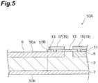
- FIGS. 5 to 7 illustrate each configuration in the cross section of the semiconductor wafer 50 illustrated in FIG. 4 .
- the semiconductor wafer 50A is the semiconductor wafer 50 before processing, and is a first conductivity type silicon substrate.
- the semiconductor region 5 of the second conductivity type is provided on the main surface 50a side of the semiconductor region 3.
- the semiconductor region 5 is provided on the main surface 50a side by adding the second conductivity type impurities from the main surface 50a to the semiconductor wafer 50A using an ion implantation method.
- the energy ray sensitive region ⁇ is formed from the semiconductor region 3 and the semiconductor region 5.
- the semiconductor region 7 of the fist conductivity type, having a higher impurity concentration than the semiconductor region 3, is provided on the main surface 50b side of the semiconductor region.
- the semiconductor region 7 is provided on the main surface 50b side by adding first conductivity type impurities from the main surface 50b to the semiconductor wafer 50A using an ion implantation method.
- the semiconductor region 7 is provided such that the length T1 of the semiconductor region 7 in the thickness direction of the semiconductor region 7 is smaller than the length T2 of the semiconductor region 5 in the thickness direction of the semiconductor region 5.
- the insulating film 13 is formed on the main surface 50a so as to cover the main surface 50a of the semiconductor wafer 50A.
- the insulating film 13 is formed by, for example, a thermal oxidation method, a sputtering method, or a Plasma-enhanced Chemical Vapor Deposition (PECVD) method.
- PECVD Plasma-enhanced Chemical Vapor Deposition
- the electrodes 15 and 17 are formed by removing a part of the insulating film 13 formed on the semiconductor region 5 and the semiconductor region 9 and then providing a metal layer 19 on the semiconductor region 5 and the semiconductor region 9.
- electrodes connected to the semiconductor region 7 are formed by forming an insulating film on the main surface 50b, removing a part of the insulating film, and then forming a metal layer on the semiconductor region 7.
- a virtual cutting line 53A and a virtual cutting line 53B that define the chip portion 51 as viewed from a direction (thickness direction) perpendicular to the main surface 50a are set.
- the outer edge of the chip portion 51 is defined by the virtual cutting line 53A and the virtual cutting line 53B.
- the shortest distance L1 from the virtual cutting line 53B to the edge of the semiconductor region 5 closest to the virtual cutting line 53B is smaller than the shortest distance L2 from the virtual cutting line 53A to the edge of the semiconductor region 5 closest to the virtual cutting line 53A.
- the shortest distance from the virtual cutting line 53B to the edge of the semiconductor region 5 is smaller than the shortest distance from the virtual cutting line 53A to the edge of the semiconductor region 5.
- the side surface 50c to which the semiconductor region 3 is exposed is formed in the chip portion 51 by providing the through-slit penetrating through the semiconductor wafer 50A in the thickness direction along the virtual cutting line 53B.
- the through-slit ⁇ is provided by dry etching on the semiconductor wafer 50A.
- the semiconductor region 11 of the first conductivity type is provided on the side surface 50c side by adding first conductivity type impurities from the side surface 50c to the chip portion 51 through the through-slit ⁇ using an ion implantation method.
- the arrows illustrated in FIG. 7 indicate the direction of impurity implantation.
- the impurities are implanted from a direction crossing the side surface 50c. The larger the width of the through-slit ⁇ , the larger the inclination of the impurity implantation direction with respect to the side surface 50c.
- the semiconductor region 5, the semiconductor region 7, the semiconductor region 9, and the semiconductor region 11 may be provided by adding impurities using a diffusion method instead of the ion implantation method.
- the passivation film 21 is provided on the main surface 50a side of the semiconductor wafer 50A so as to cover the insulating film 13 and the electrodes 15 and 17.
- the passivation film 21 is formed by, for example, a Chemical Vapor Deposition (CVD) method.
- CVD Chemical Vapor Deposition
- the bump electrode 23 is provided.
- Each bump electrode 23 is electrically connected to the corresponding electrode 15.
- a method of forming the bump electrode 23 a method of mounting a solder ball or a printing method can be used.
- the semiconductor wafer 50 is manufactured by the above-described manufacturing method. Using the semiconductor wafer 50, the semiconductor energy ray detecting element ED1 can be manufactured.
- the semiconductor wafer 50 is prepared, a plurality of pad electrodes 25 provided in the ROIC chip RC are connected to the corresponding bump electrodes 23, and then the chip portion 51 is cut off along the virtual cutting line 53 (virtual cutting line 53A) of the semiconductor wafer 50.
- the cut chip portion 51 functions as the semiconductor energy ray detecting element ED1.
- the blank portion 52 and the chip portion 51 are cut off by cutting along the virtual cutting line 53 (virtual cutting line 53A) using a cutting tool generally used.
- the cutting tool used is a dicing saw, for example.
- the shortest distance from the virtual cutting line 53B to the edge of the semiconductor region 5 is set to be smaller than the shortest distance from the virtual cutting line 53A to the edge of the semiconductor region 5.
- the side surface 50c to which the semiconductor region 3 is exposed is formed in the semiconductor wafer 50A by providing the through-slit along the virtual cutting line 53B, and the semiconductor region 11 of the first conductivity type is provided on the side surface 50c. Therefore, the semiconductor wafer 50 manufactured by this manufacturing method has the chip portion 51 in which the dead area is reduced and an increase in leakage current from the side surface 50c can be suppressed by the semiconductor region 11.
- the passivation film 21, patterning, the bump electrode 23, and the like are formed after providing the semiconductor region 11 of first conductivity type on the side surface 50c that is exposed by providing the through-slit ⁇ .
- the passivation film 21, the patterning, the bump electrode 23, and the like are formed, the semiconductor region 11 is already provided in the semiconductor wafer 50A. Therefore, the passivation film 21, the patterning, the bump electrode 23, and the like can be easily formed.
- the through-slit ⁇ is provided by dry etching.
- the inclination of the side surface 50c can be reduced compared with a case where the through-slit ⁇ is provided by wet etching. Therefore, the dead area can be reduced compared with a case where the side surface is made to be inclined by using wet etching.
- the time and effort of forming the side surface 1c (side surface 50c of the chip portion 51) in the semiconductor energy ray detecting element ED1 can be reduced.
- a step of providing a metal layer on the main surface 50a and the main surface 50b is further included, and impurities are added to the side surface 50c of the semiconductor wafer 50A by ion implantation after the metal layer is provided.
- impurities are added by ion implantation, heat applied to the semiconductor wafer 50A can be reduced compared with a case where the impurities are added by diffusion. Therefore, it is possible to manufacture the semiconductor wafer 50 in which the metal layer can be appropriately formed and the impurities are sufficiently added.
- the semiconductor region 7 is provided such that the length T1 of the semiconductor region 7 in the thickness direction of the semiconductor region 7 is smaller than the length T2 of the semiconductor region 5 in the thickness direction of the semiconductor region 5.
- energy rays having low light transmittance such as soft X-rays
- detection accuracy is improved for energy rays having low light transmittance, such as soft X-rays.
- the impurities are blocked by the hole bottom, and accordingly there is a possibility that the impurities will not be added to the entire side surface 50c.
- the semiconductor region 7 and the semiconductor region 11 are unlikely to be connected to each other, and accordingly there is a possibility that a region where no impurities are added will be present.
- the depletion layer may reach the side surface 1c through the region.
- the semiconductor region 11 is formed by adding impurities to the side surface 50c that is exposed by providing the through-slit ⁇ , the semiconductor region 7 and the semiconductor region 11 are easily and appropriately connected to each other, and accordingly an increase in leakage current can be suppressed.
- the semiconductor energy ray detecting element ED1 is manufactured by preparing the semiconductor wafer 50 manufactured by the above-described manufacturing method and cutting off the chip portion 51 along the virtual cutting line 53A.
- the dead area is reduced, and an increase in leakage current from the side surface 50c can be suppressed by the semiconductor region 11. Since impurities are added to the side surface 50c that is exposed by providing the through-slit ⁇ , the impurities are added more appropriately than in a case where the impurities are added from holes.
- the shortest distance from the virtual cutting line 53B to the edge of the semiconductor region 5 is set to be smaller than the shortest distance from the virtual cutting line 53A to the edge of the semiconductor region 5.
- the shortest distance from the virtual cutting line 53A to the edge of the semiconductor region 5 is set to be larger than the shortest distance from the virtual cutting line 53B to the edge of the semiconductor region 5.
- the depletion layer spreads from the semiconductor region 5. Therefore, in the semiconductor energy ray detecting element ED1, the depletion layer is unlikely to reach a cut surface along the virtual cutting line 53A.
- the chip portion 51 has the semiconductor region 11 located on the side surface 50c.
- the shortest distance from the side surface 50c to the edge of the semiconductor region 5 is smaller than the shortest distance from the virtual cutting line 53 (virtual cutting line 53A) to the edge of the semiconductor region 5. Therefore, cutting the chip portion 51 with the virtual cutting line 53 (virtual cutting line 53A) makes it possible to manufacture the semiconductor energy ray detecting element ED1 in which the dead area is reduced and in which an increase in leakage current from the side surface 50c in the semiconductor region 11 can be suppressed.
- one chip portion 51 is disposed on one semiconductor wafer 50.
- the number of chip portions 51 disposed on the semiconductor wafer 50 is not limited to one.
- a plurality of chip portions 51 may be disposed on one semiconductor wafer 50.
- the semiconductor substrate 1 and the chip portion 51 are rectangular in plan view in the embodiment described above, but are not limited to this.
- the semiconductor substrate 1 and the chip portion 51 may be hexagonal in plan view.
- the through-slit ⁇ may be provided along five sides of the six sides of the edge of the chip portion 51, and the virtual cutting line 53 may be set along the remaining one side.
- the order in which the semiconductor region 5, the semiconductor region 7, the semiconductor region 9, and the semiconductor region 11 are provided is not limited to the order described in the present embodiment.
- the semiconductor region 9 may not be provided.
- the semiconductor region 11 provided on the side surface 50c side is adjacent to the semiconductor region 3.
- the order in which the insulating film 13, the electrodes 15 and 17, the passivation film 21, the bump electrode 23, and the through-slit ⁇ are provided is not limited to that described in the present embodiment.
- the through-slit ⁇ may be provided after the bump electrode 23 is provided.
- the insulating film 13, the electrodes 15 and 17, the passivation film 21, and the bump electrode 23 may be provided not in the step of manufacturing the semiconductor wafer 50 but in the step of manufacturing the semiconductor energy ray detecting element ED1 using the semiconductor wafer 50.
- the semiconductor substrate 1 and the semiconductor wafer 50 may be configured by reversing the positions of the semiconductor region of the first conductive type and the semiconductor region of the second conductive type.
Landscapes
- Physics & Mathematics (AREA)
- Health & Medical Sciences (AREA)
- Life Sciences & Earth Sciences (AREA)
- General Physics & Mathematics (AREA)
- High Energy & Nuclear Physics (AREA)
- Molecular Biology (AREA)
- Spectroscopy & Molecular Physics (AREA)
- Light Receiving Elements (AREA)
- Measurement Of Radiation (AREA)
Abstract
Description
- The present invention relates to a semiconductor wafer manufacturing method, a method of manufacturing a semiconductor energy ray detecting element, and a semiconductor wafer.
-
Patent Literature 1 discloses a semiconductor wafer manufacturing method. In this manufacturing method, a plurality of holes are formed in the semiconductor wafer along virtual cutting lines for separating elements from the semiconductor wafer. Impurities are added to the semiconductor wafer through the plurality of holes. As a result, a region where impurities are added is formed around each hole. - Patent Literature 1: Japanese Unexamined Patent Publication No.
2015-19540 - A known semiconductor energy ray detecting element includes a semiconductor substrate having a first main surface and a second main surface facing each other. In this semiconductor energy ray detecting element, the semiconductor substrate has a first semiconductor region of a first conductivity type, being located on the first main surface side, a second semiconductor region of a second conductivity type, being located on the first main surface side and forming an energy ray sensitive region together with the first semiconductor region, and a third semiconductor region of the first conductivity type, being located on the second main surface side and having a higher impurity concentration than the first semiconductor region.
- In order to operate the semiconductor energy ray detecting element described above, a bias voltage is applied to the semiconductor energy ray detecting element. The bias voltage is about several tens to one thousand volts, for example. In this case, the first semiconductor region needs to be in a fully depleted state in which a depletion layer spreading from the second semiconductor region reaches an interface with the third semiconductor region from the first main surface side. When the semiconductor substrate (first semiconductor region) is fully depleted, if the depletion layer reaches the side surface of the semiconductor substrate (first semiconductor layer), the leakage current from the side surface may increase. For this reason, it is conceivable that the distance between the side surface and the second semiconductor region is set to a relatively large value so that the depletion layer does not reach the side surface even in a case where the first semiconductor layer is fully depleted.
- A region between the side surface and the second semiconductor region in the semiconductor substrate is a region that is unlikely to contribute to detection of energy rays. Hereinafter, the region that is unlikely to contribute to detection of energy rays is referred to as a "dead area". If the dead area can be reduced, it is possible to expand a region that contributes to detection of energy rays. Hereinafter, a region that contributes to detection of energy rays is referred to as an "effective area". However, if the dead area is reduced, there is a concern about an increase in leakage current from the side surface due to the depletion layer described above. Therefore, in order to suppress the depletion layer from reaching the side surface of the semiconductor substrate in a state where the semiconductor substrate (first semiconductor layer) is fully depleted, it is conceivable that a fourth semiconductor region of the first conductivity type, having a higher impurity concentration than the first semiconductor region and provided on the side surface side of the semiconductor substrate.
- In a case where the method disclosed in
Patent Literature 1 is applied to form the fourth semiconductor region, the following problems may occur. In a case where the diameter of the hole is small, it is difficult for impurities to be added to the semiconductor wafer, and accordingly there is a possibility that a region where no impurities are added will be present along a virtual cutting line. In a case where a region where no impurities are added is present, the depletion layer may reach the side surface through the region. In a case where the diameter of the hole is large, impurities are easily added to the semiconductor wafer, but the thickness of the region where impurities are added, that is, the thickness of the fourth semiconductor region may need to be increased. Since the fourth semiconductor region is a dead area, the effective area is reduced if the thickness of the fourth semiconductor region is increased. - A first aspect of the present invention is to provide a semiconductor wafer manufacturing method used for manufacturing a semiconductor energy detecting element capable of suppressing an increase in leakage current from the side surface while a dead area is reduced. A second aspect of the present invention is to provide a method of manufacturing a semiconductor energy ray detecting element using a semiconductor wafer used for manufacturing a semiconductor energy detecting element capable of suppressing an increase in leakage current from the side surface while a dead area is reduced. A third aspect of the present invention is to provide a semiconductor wafer used for manufacturing a semiconductor energy detecting element capable of suppressing an increase in leakage current from the side surface while a dead area is reduced.
- The first aspect of the present invention is a semiconductor wafer manufacturing method. In the first aspect, a semiconductor wafer having a first semiconductor region of a first conductivity type including a first main surface and a second main surface facing each other is prepared. A second semiconductor region of a second conductivity type, forming an energy ray sensitive region together with the first semiconductor region, is provided on the first main surface side of the first semiconductor region. A third semiconductor region of the first conductivity type, having a higher impurity concentration than the first semiconductor region, is provided on the second main surface side of the first semiconductor region. A through-slit penetrating through the semiconductor wafer in a thickness direction of the semiconductor wafer along a second virtual cutting line of a first virtual cutting line and the second virtual cutting line, as viewed from a direction perpendicular to the first main surface, is provided. The first virtual cutting line defines a chip portion including the energy ray sensitive region. A shortest distance from the second virtual cutting line to an edge of the second semiconductor region is smaller than a shortest distance from the first virtual cutting line to the edge of the second semiconductor region. A side surface to which the first semiconductor region is exposed is formed in the chip portion by providing the through-slit. A fourth semiconductor region of a first conductivity type is provided on the side surface side by adding impurities to the side surface.
- In the first aspect, as viewed from the direction perpendicular to the first main surface, the shortest distance from the second virtual cutting line to the edge of the second semiconductor region is set to be smaller than the shortest distance from the first virtual cutting line to the edge of the second semiconductor region. In this manufacturing method, the side surface to which the first semiconductor region is exposed is formed in the semiconductor wafer by providing the through-slit along the second virtual cutting line, and the fourth semiconductor region of the first conductivity type is provided on the side surface. Therefore, the semiconductor wafer manufactured by this manufacturing method has a chip portion in which the dead area is reduced and an increase in leakage current from the side surface can be suppressed by the fourth semiconductor region. Since impurities are added to the side surface that is exposed by providing the through-slit, the impurities are added more appropriately than in a case where the impurities are added from holes.
- In the first aspect, the through-slit may be provided by dry etching. In this case, the inclination of the side surface can be reduced compared with a case where the through-slit is provided by wet etching. Therefore, the dead area can be reduced compared with a case where the side surface is made to be inclined by using wet etching.
- In the first aspect, a metal layer may be provided on the first main surface and the second main surface. The impurities may be added to the side surface of the chip portion by ion implantation after the metal layer is provided. In this case, since the impurities are added by ion implantation, heat applied to the semiconductor wafer can be reduced compared with a case where the impurities are added by diffusion. Therefore, it is possible to manufacture the semiconductor wafer in which the metal layer can be appropriately formed and the impurities are sufficiently added.
- In the first aspect, the third semiconductor region may be provided such that a length of the third semiconductor region in a thickness direction of the third semiconductor region is smaller than a length of the second semiconductor region in a thickness direction of the second semiconductor region. In this case, for example, energy rays having low light transmittance, such as soft X-rays, are unlikely to be absorbed in the third semiconductor region, so that the detection accuracy is improved. In this manufacturing method, impurities are added to the side surface that is exposed by providing the through-slit. For this reason, also in this case, the third semiconductor region and the fourth semiconductor region are easily and appropriately connected to each other, and accordingly an increase in leakage current can be suppressed.
- The second aspect of the present invention is a method of manufacturing a semiconductor energy ray detecting element. In the second aspect, a semiconductor wafer manufactured by the manufacturing method described above is prepared. The chip portion is cut off along the first virtual cutting line.
- In the second aspect, as viewed from the direction perpendicular to the first main surface, the shortest distance from the second virtual cutting line to the edge of the second semiconductor region is set to be smaller than the shortest distance from the first virtual cutting line to the edge of the second semiconductor region. A side surface to which the first semiconductor region is exposed is formed in the semiconductor wafer by providing the through-slit along the second virtual cutting line. A fourth semiconductor region of the first conductivity type is provided on the side surface. Therefore, in the semiconductor energy ray detecting element manufactured by this manufacturing method, the dead area is reduced, and an increase in leakage current from the side surface can be suppressed by the fourth semiconductor region. Since impurities are added to the side surface that is exposed by providing the through-slit, the impurities can be added more appropriately than in a case where the impurities are added from holes. The shortest distance from the second virtual cutting line to the edge of the second semiconductor region is set to be smaller than the shortest distance from the first virtual cutting line to the edge of the second semiconductor region. That is, the shortest distance from the first virtual cutting line to the edge of the second semiconductor region is set to be larger than the shortest distance from the second virtual cutting line to the edge of the second semiconductor region. Therefore, it is suppressed that the depletion layer reaches a cut surface along the first virtual cutting line.
- The third aspect of the present invention is a semiconductor wafer. The semiconductor wafer has a first main surface and a second main surface that facing each other. The semiconductor wafer includes a chip portion. The chip portion includes an energy ray sensitive region and is defined by a through-slit penetrating in a thickness direction and a virtual cutting line as viewed from a direction perpendicular to the first main surface. The chip portion has a first semiconductor region of a first conductivity type, a second semiconductor region of a second conductivity type, a third semiconductor region of the first conductivity type, and a fourth semiconductor region of the first conductivity type. The first semiconductor region is located on the first main surface side. The second semiconductor region is located on the first main surface side, and forms the energy ray sensitive region together with the first semiconductor region. The third semiconductor region is located on the second main surface side, and has a higher impurity concentration than the first semiconductor region. The fourth semiconductor region is located on a side surface side connected to the first main surface and the second main surface, and has a higher impurity concentration than the first semiconductor region. The shortest distance from the side surface of the chip portion to the edge of the second semiconductor region is smaller than the shortest distance from the virtual cutting line to the edge of the second semiconductor region.
- In the third aspect, the chip portion has the fourth semiconductor region located on the side surface. The shortest distance from the side surface of the chip portion to the edge of the second semiconductor region is smaller than the shortest distance from the virtual cutting line to the edge of the second semiconductor region. Therefore, cutting the chip portion with the virtual cutting line makes it possible to manufacture the semiconductor energy ray detecting element in which the dead area is reduced and in which an increase in leakage current from the side surface in the fourth semiconductor region can be suppressed.
- According to the first aspect of the present invention, there is provided a semiconductor wafer manufacturing method used for manufacturing a semiconductor energy detecting element capable of suppressing an increase in leakage current from the side surface while a dead area is reduced. According to the second aspect of the present invention, there is provided a method of manufacturing a semiconductor energy ray detecting element using a semiconductor wafer used for manufacturing a semiconductor energy detecting element capable of suppressing an increase in leakage current from the side surface while a dead area is reduced. According to the third aspect of the present invention, there is provided a semiconductor wafer used for manufacturing a semiconductor energy detecting element capable of suppressing an increase in leakage current from the side surface while a dead area is reduced.
-
-
FIG. 1 is a diagram for describing the cross-sectional configuration of a semiconductor energy ray detecting element according to an embodiment. -
FIG. 2 is a schematic plan view illustrating an arrangement example of semiconductor energy ray detecting elements. -
FIG. 3 is a schematic plan view of a semiconductor wafer. -
FIG. 4 is a diagram illustrating the cross-sectional configuration of a semiconductor wafer. -
FIG. 5 is a diagram illustrating a semiconductor wafer manufacturing method. -
FIG. 6 is a diagram illustrating a semiconductor wafer manufacturing method. -
FIG. 7 is a diagram illustrating a semiconductor wafer manufacturing method. - Hereinafter, an embodiment of the present invention will be described in detail with reference to the accompanying diagrams. In addition, in the description, the same reference numerals are used for the same elements or elements having the same functions, and the repeated description thereof will be omitted.
- With reference to
FIGS. 1 and2 , the configuration of a semiconductor energy ray detecting element ED1 according to the present embodiment will be described.FIG. 1 is a diagram for describing the cross-sectional configuration of the semiconductor energy ray detecting element according to the present embodiment.FIG. 2 is a schematic plan view illustrating an arrangement example of semiconductor energy ray detecting elements. - The semiconductor energy ray detecting element ED1 includes a
semiconductor substrate 1 as illustrated inFIG. 1 . Thesemiconductor substrate 1 is a first conductivity type silicon substrate having a pair ofmain surfaces side surface 1d. The first conductivity type is, for example, n-type. The plurality ofside surfaces 1c and aside surface 1d extend in a direction in which the pair ofmain surfaces main surfaces main surfaces - As illustrated in
FIG. 2 , thesemiconductor substrate 1 has a rectangular shape in plan view. In the present embodiment, a plurality of semiconductor energy ray detecting elements ED1 form a semiconductor energy ray detecting element group ED 10. The semiconductor energy ray detecting element group ED10 includes a plurality of semiconductor energy ray detecting elements ED1. The plurality of semiconductor energy ray detecting elements ED1 are arranged in a two-dimensional matrix as viewed from the thickness direction. Specifically, eight semiconductor energy ray detecting elements ED1 are arranged in two rows and four columns with the side surfaces 1c adjacent to each other. Side surfaces 10a and 10b facing each other of the outer frame of the semiconductor energy ray detecting element group ED10 are formed by the side surfaces 1c, andside surfaces - As illustrated in
FIG. 1 , the semiconductor energy ray detecting element ED1 has an insulatingfilm 13 andelectrodes semiconductor substrate 1. The insulatingfilm 13 is provided on themain surface 1a side of thesemiconductor substrate 1 so as to cover themain surface 1a of thesemiconductor substrate 1. The insulatingfilm 13 is formed of, for example, SiO2. Theelectrodes film 13. Theelectrodes main surface 1b side of thesemiconductor substrate 1. - The semiconductor energy ray detecting element ED1 further has a
passivation film 21 and abump electrode 23. Thepassivation film 21 is disposed on themain surface 1a side of thesemiconductor substrate 1 so as to cover themain surface 1a of thesemiconductor substrate 1, the insulatingfilm 13, and theelectrodes passivation film 21 is formed of, for example, SiN. Thebump electrode 23 is disposed on theelectrode 15, and is electrically connected to the correspondingelectrode 15 from a portion where thepassivation film 21 is partially removed. Thebump electrode 23 is formed of, for example, Sn-Ag. - The semiconductor energy ray detecting element ED1 is mounted on an ROIC chip RC as illustrated in
FIG. 1 . Specifically, the semiconductor energy ray detecting element ED1 is bump-connected to the ROIC chip RC. The ROIC chip RC includes a plurality ofpad electrodes 25, and thepad electrode 25 and thebump electrode 23 corresponding to each other are connected. The semiconductor energy ray detecting element ED1 and the ROIC chip RC are disposed close to each other. Themain surface 1a of thesemiconductor substrate 1 faces the ROIC chip RC. - In the semiconductor energy ray detecting element ED1, in the embodiment described above, the
main surface 1a of thesemiconductor substrate 1 may be a surface where energy rays are incident on the semiconductor substrate 1 (incidence surface), or themain surface 1b of thesemiconductor substrate 1 may be the incidence surface. In the present embodiment, themain surface 1b of thesemiconductor substrate 1 is an incidence surface. - In the semiconductor energy ray detecting element ED1, when a bias voltage is applied to the
semiconductor substrate 1, a depletion layer spreads in thesemiconductor substrate 1 to cause a fully depleted state. The voltage applied to thesemiconductor substrate 1 is, for example, a reverse bias voltage. Causing the fully depleted state may allow a signal corresponding to the energy ray to be appropriately output from the semiconductor energy ray detecting element ED1 to the ROIC chip RC. - Next, the configuration of a
semiconductor wafer 50 used for manufacturing of thesemiconductor substrate 1 of the semiconductor energy ray detecting element ED1 will be described with reference toFIGS. 3 and4 .FIG. 3 is a schematic plan view of thesemiconductor wafer 50.FIG. 4 is a schematic cross-sectional view taken along the line IV-IV of thesemiconductor wafer 50 illustrated inFIG. 3 . - The
semiconductor wafer 50 has a circular shape in plan view, and has a pair ofmain surfaces FIG. 3 , thesemiconductor wafer 50 includes achip portion 51 including an energy ray sensitive region α and ablank portion 52 excluding thechip portion 51. Thechip portion 51 has a rectangular shape in plan view, and is disposed near the center of thesemiconductor wafer 50. Theblank portion 52 is disposed so as to surround thechip portion 51. - The
chip portion 51 is defined by a through-slit β penetrating in the thickness direction and avirtual cutting line 53 as viewed from a direction (thickness direction) perpendicular to themain surface 50a. Thechip portion 51 and theblank portion 52 are connected by thevirtual cutting line 53. In the present embodiment, the through-slit β is provided along three sides of the four sides of the edge of thechip portion 51, and thevirtual cutting line 53 is set along the remaining one side. Thesemiconductor substrate 1 is formed by cutting thesemiconductor wafer 50 along thevirtual cutting line 53 to cut off thechip portion 51. As illustrated inFIG. 4 , thechip portion 51 has aside surface 50c connected to themain surface 50a and themain surface 50b along the through-slit β. - The
chip portion 51 has asemiconductor region 3 of a first conductivity type, being located on themain surface 50a side and a plurality ofsemiconductor regions 5 of a second conductivity type, being located on themain surface 50a side. The first conductivity type is, for example, n-type, and the second conductivity type is, for example, p-type. Thesemiconductor region 3 is a region where first conductivity type impurities are added. The first conductivity type impurities added to thesemiconductor region 3 are, for example, antimony, arsenic, or phosphorus. Thesemiconductor region 3 is also provided in theblank portion 52. Thesemiconductor region 3 in thechip portion 51 is connected to thesemiconductor region 3 in theblank portion 52 through thevirtual cutting line 53. The plurality ofsemiconductor regions 5 are arranged in a two-dimensional matrix as viewed from the thickness direction. - A part of the
semiconductor region 3 is interposed between thesemiconductor regions 5. Thesemiconductor regions 5 are separated from each other. Eachsemiconductor region 5 is a region where second conductivity type impurities are added, and has a higher impurity concentration than thesemiconductor region 3. The second conductivity type impurities are, for example, boron. Thesemiconductor region 3 and eachsemiconductor region 5 form the energy ray sensitive region α by p-n junctions. - The
chip portion 51 further has asemiconductor region 7 of the first conductivity type, being located on themain surface 50b side. Thesemiconductor region 7 has a higher impurity concentration than thesemiconductor region 3. Thesemiconductor region 7 is a region where the first conductivity type impurities are added, and has a higher impurity concentration than thesemiconductor region 3. The first conductivity type impurities added to thesemiconductor region 7 are, for example, antimony, arsenic, or phosphorus. - The
semiconductor region 7 is also provided on themain surface 50b side of theblank portion 52. Thesemiconductor region 7 at the outer edge of thechip portion 51 is connected to thesemiconductor region 7 of theblank portion 52 through thevirtual cutting line 53. The length T1 of thesemiconductor region 7 in the thickness direction of thesemiconductor region 7 is smaller than the length T2 of thesemiconductor region 5 in the thickness direction of thesemiconductor region 5. - The
chip portion 51 has asemiconductor region 9 of the first conductivity type on themain surface 50a side. Thesemiconductor region 9 is also a region where the first conductivity type impurities are added, and has a higher impurity concentration than thesemiconductor region 3. The first conductivity type impurities added to thesemiconductor region 9 are, for example, antimony, arsenic, or phosphorus. Thesemiconductor region 9 is also provided on themain surface 50a side of theblank portion 52. Thesemiconductor region 9 at the outer edge of thechip portion 51 is connected to thesemiconductor region 9 of theblank portion 52 through thevirtual cutting line 53. - The
semiconductor region 9 of thechip portion 51 is located so as to surround the periphery of a region, in which the plurality ofsemiconductor regions 5 are located, along the outer edge of thechip portion 51 on themain surface 50a side as viewed from the thickness direction. Thesemiconductor region 9 of thechip portion 51 functions as a guard ring. In thechip portion 51, a part of thesemiconductor region 3 is interposed between thesemiconductor region 5 and thesemiconductor region 9. Thesemiconductor region 5 and thesemiconductor region 9 are separated from each other. - As illustrated in
FIG. 4 , a shortest distance L1 is smaller than a shortest distance L2. The shortest distance L1 is the shortest distance from theside surface 50c to the edge of thesemiconductor region 5 closest to theside surface 50c. The shortest distance L2 is the shortest distance from thevirtual cutting line 53 to the edge of thesemiconductor region 5 closest to thevirtual cutting line 53. The shortest distance from theside surface 50c to the edge of thesemiconductor region 5 is smaller than the shortest distance from thevirtual cutting line 53 to the edge of thesemiconductor region 5. As described above, thesemiconductor region 5 forms the energy ray sensitive region α. Therefore, the shortest distance from theside surface 50c to the energy ray sensitive region α is smaller than the shortest distance from thevirtual cutting line 53 to the energy ray sensitive region α. - The
chip portion 51 has the insulatingfilm 13 that covers themain surface 50a, and has theelectrodes semiconductor region 5, thesemiconductor region 7, and thesemiconductor region 9. From a portion where the insulatingfilm 13 is partially removed, theelectrode 15 is connected to thesemiconductor region 5, and theelectrode 17 is connected to thesemiconductor region 9. Although not illustrated, an electrode connected to thesemiconductor region 7 is also formed on themain surface 50b side. Thechip portion 51 further has thepassivation film 21 that covers the insulatingfilm 13 and theelectrodes bump electrode 23 electrically connected to theelectrode 15 from a portion where thepassivation film 21 is partially removed on theelectrode 15. - The
chip portion 51 has asemiconductor region 11 of the first conductivity type, being located on theside surface 50c side. Thesemiconductor region 11 has a higher impurity concentration than thesemiconductor region 3. Thesemiconductor region 11 is connected to thesemiconductor region 7 and thesemiconductor region 9. Thesemiconductor region 11 is exposed to theside surface 50c, and forms at least a part of theside surface 50c. In the present embodiment, thesemiconductor region 7, thesemiconductor region 9, and thesemiconductor region 11 are exposed to theside surface 50c, and thesemiconductor region 7, thesemiconductor region 9, and thesemiconductor region 11 form theside surface 50c. Theside surface 50c is formed by a semiconductor region having a higher impurity concentration than thesemiconductor region 3. Thesemiconductor region 3 is not exposed to theside surface 50c. Thesemiconductor region 11 may form theentire side surface 50c. - The
chip portion 51 of thesemiconductor wafer 50 having the above-described configuration functions as the semiconductor energy ray detecting element ED1. When a bias voltage is applied between thesemiconductor region 5 and thesemiconductor region 7, a depletion layer spreads from thesemiconductor region 5 to thesemiconductor region 3. The bias voltage applied between thesemiconductor region 5 and thesemiconductor region 7 is, for example, a reverse bias voltage. A state in which the depletion layer reaches thesemiconductor region 7 is a fully depleted state. Causing the fully depleted state may allow a signal corresponding to the energy ray to be output from the semiconductor energy ray detecting element ED1. - Next, an example of a method of manufacturing the
semiconductor wafer 50 will be described with reference toFIGS. 5 to 7. FIGS. 5 to 7 illustrate each configuration in the cross section of thesemiconductor wafer 50 illustrated inFIG. 4 . - First, a
semiconductor wafer 50A having thesemiconductor region 3 of the first conductivity type, including amain surface 50a and amain surface 50b facing each other, is prepared. Thesemiconductor wafer 50A is thesemiconductor wafer 50 before processing, and is a first conductivity type silicon substrate. - Then, the
semiconductor region 5 of the second conductivity type is provided on themain surface 50a side of thesemiconductor region 3. In the present embodiment, thesemiconductor region 5 is provided on themain surface 50a side by adding the second conductivity type impurities from themain surface 50a to thesemiconductor wafer 50A using an ion implantation method. As a result, the energy ray sensitive region α is formed from thesemiconductor region 3 and thesemiconductor region 5. - Then, the
semiconductor region 7 of the fist conductivity type, having a higher impurity concentration than thesemiconductor region 3, is provided on themain surface 50b side of the semiconductor region. In the present embodiment, thesemiconductor region 7 is provided on themain surface 50b side by adding first conductivity type impurities from themain surface 50b to thesemiconductor wafer 50A using an ion implantation method. Thesemiconductor region 7 is provided such that the length T1 of thesemiconductor region 7 in the thickness direction of thesemiconductor region 7 is smaller than the length T2 of thesemiconductor region 5 in the thickness direction of thesemiconductor region 5. - Then, the insulating
film 13 is formed on themain surface 50a so as to cover themain surface 50a of thesemiconductor wafer 50A. The insulatingfilm 13 is formed by, for example, a thermal oxidation method, a sputtering method, or a Plasma-enhanced Chemical Vapor Deposition (PECVD) method. Then, theelectrodes film 13 formed on thesemiconductor region 5 and thesemiconductor region 9 and then providing ametal layer 19 on thesemiconductor region 5 and thesemiconductor region 9. Although not illustrated, similar to the formation of the insulatingfilm 13 and theelectrodes semiconductor region 7 are formed by forming an insulating film on themain surface 50b, removing a part of the insulating film, and then forming a metal layer on thesemiconductor region 7. - Here, as illustrated in
FIGS. 4 and5 , avirtual cutting line 53A and avirtual cutting line 53B that define thechip portion 51 as viewed from a direction (thickness direction) perpendicular to themain surface 50a are set. The outer edge of thechip portion 51 is defined by thevirtual cutting line 53A and thevirtual cutting line 53B. The shortest distance L1 from thevirtual cutting line 53B to the edge of thesemiconductor region 5 closest to thevirtual cutting line 53B is smaller than the shortest distance L2 from thevirtual cutting line 53A to the edge of thesemiconductor region 5 closest to thevirtual cutting line 53A. The shortest distance from thevirtual cutting line 53B to the edge of thesemiconductor region 5 is smaller than the shortest distance from thevirtual cutting line 53A to the edge of thesemiconductor region 5. - Then, as illustrated in
FIG. 6 , theside surface 50c to which thesemiconductor region 3 is exposed is formed in thechip portion 51 by providing the through-slit penetrating through thesemiconductor wafer 50A in the thickness direction along thevirtual cutting line 53B. In the present embodiment, the through-slit β is provided by dry etching on thesemiconductor wafer 50A. - Then, impurities are added to the
side surface 50c to provide thesemiconductor region 11 of the first conductivity type of theside surface 50c side. In the present embodiment, as illustrated inFIG. 7 , thesemiconductor region 11 of the first conductivity type is provided on theside surface 50c side by adding first conductivity type impurities from theside surface 50c to thechip portion 51 through the through-slit β using an ion implantation method. The arrows illustrated inFIG. 7 indicate the direction of impurity implantation. The impurities are implanted from a direction crossing theside surface 50c. The larger the width of the through-slit β, the larger the inclination of the impurity implantation direction with respect to theside surface 50c. Thesemiconductor region 5, thesemiconductor region 7, thesemiconductor region 9, and thesemiconductor region 11 may be provided by adding impurities using a diffusion method instead of the ion implantation method. - Then, the
passivation film 21 is provided on themain surface 50a side of thesemiconductor wafer 50A so as to cover the insulatingfilm 13 and theelectrodes passivation film 21 is formed by, for example, a Chemical Vapor Deposition (CVD) method. Then, after removing a part of thepassivation film 21 formed on eachelectrode 15, thebump electrode 23 is provided. Eachbump electrode 23 is electrically connected to the correspondingelectrode 15. As a method of forming thebump electrode 23, a method of mounting a solder ball or a printing method can be used. - The
semiconductor wafer 50 is manufactured by the above-described manufacturing method. Using thesemiconductor wafer 50, the semiconductor energy ray detecting element ED1 can be manufactured. In the present embodiment, thesemiconductor wafer 50 is prepared, a plurality ofpad electrodes 25 provided in the ROIC chip RC are connected to thecorresponding bump electrodes 23, and then thechip portion 51 is cut off along the virtual cutting line 53 (virtual cutting line 53A) of thesemiconductor wafer 50. Thecut chip portion 51 functions as the semiconductor energy ray detecting element ED1. In the present embodiment, theblank portion 52 and thechip portion 51 are cut off by cutting along the virtual cutting line 53 (virtual cutting line 53A) using a cutting tool generally used. The cutting tool used is a dicing saw, for example. - As described above, in the method of manufacturing the
semiconductor wafer 50, as viewed from the direction perpendicular to themain surface 50a, the shortest distance from thevirtual cutting line 53B to the edge of thesemiconductor region 5 is set to be smaller than the shortest distance from thevirtual cutting line 53A to the edge of thesemiconductor region 5. In this manufacturing method, theside surface 50c to which thesemiconductor region 3 is exposed is formed in thesemiconductor wafer 50A by providing the through-slit along thevirtual cutting line 53B, and thesemiconductor region 11 of the first conductivity type is provided on theside surface 50c. Therefore, thesemiconductor wafer 50 manufactured by this manufacturing method has thechip portion 51 in which the dead area is reduced and an increase in leakage current from theside surface 50c can be suppressed by thesemiconductor region 11. - As described in
Patent Literature 1, in the method of forming thesemiconductor region 11 by adding impurities from a hole that does not penetrate through thesemiconductor wafer 50, the impurities are blocked by the hole bottom, and accordingly there is a possibility that the impurities will not be added to theentire side surface 50c. In this case, the leakage current may increase from a portion where impurities are not sufficiently added in theside surface 50c. In this manufacturing method, since thesemiconductor region 11 is provided by adding impurities to theside surface 50c that is exposed by providing the through-slit β, thesemiconductor region 11 can be appropriately formed on theentire side surface 50c compared with a case where impurities are added from holes. - In the manufacturing method according to the embodiment described above, the
passivation film 21, patterning, thebump electrode 23, and the like are formed after providing thesemiconductor region 11 of first conductivity type on theside surface 50c that is exposed by providing the through-slit β. When thepassivation film 21, the patterning, thebump electrode 23, and the like are formed, thesemiconductor region 11 is already provided in thesemiconductor wafer 50A. Therefore, thepassivation film 21, the patterning, thebump electrode 23, and the like can be easily formed. - The through-slit β is provided by dry etching. In this manner, the inclination of the
side surface 50c can be reduced compared with a case where the through-slit β is provided by wet etching. Therefore, the dead area can be reduced compared with a case where the side surface is made to be inclined by using wet etching. In addition, for example, as illustrated inFIG. 2 , in a case where a plurality of semiconductor energy ray detecting elements ED1 are arranged such that the side surfaces 1c are adjacent to each other, the time and effort of forming theside surface 1c (side surface 50c of the chip portion 51) in the semiconductor energy ray detecting element ED1 can be reduced. - A step of providing a metal layer on the
main surface 50a and themain surface 50b is further included, and impurities are added to theside surface 50c of thesemiconductor wafer 50A by ion implantation after the metal layer is provided. In this manner, since the impurities are added by ion implantation, heat applied to thesemiconductor wafer 50A can be reduced compared with a case where the impurities are added by diffusion. Therefore, it is possible to manufacture thesemiconductor wafer 50 in which the metal layer can be appropriately formed and the impurities are sufficiently added. - The
semiconductor region 7 is provided such that the length T1 of thesemiconductor region 7 in the thickness direction of thesemiconductor region 7 is smaller than the length T2 of thesemiconductor region 5 in the thickness direction of thesemiconductor region 5. For example, energy rays having low light transmittance, such as soft X-rays, are unlikely to be absorbed in thesemiconductor region 7. For this reason, detection accuracy is improved for energy rays having low light transmittance, such as soft X-rays. - As described above, in the method of forming the
semiconductor region 11 by adding impurities from a hole that does not penetrate through thesemiconductor wafer 50 as described inPatent Literature 1, the impurities are blocked by the hole bottom, and accordingly there is a possibility that the impurities will not be added to theentire side surface 50c. In particular, in a case where the length of thesemiconductor region 7 in the thickness direction of thesemiconductor region 7 is reduced in order to detect energy rays having low light transmittance, thesemiconductor region 7 and thesemiconductor region 11 are unlikely to be connected to each other, and accordingly there is a possibility that a region where no impurities are added will be present. In this case, the depletion layer may reach theside surface 1c through the region. In this manufacturing method, since thesemiconductor region 11 is formed by adding impurities to theside surface 50c that is exposed by providing the through-slit β, thesemiconductor region 7 and thesemiconductor region 11 are easily and appropriately connected to each other, and accordingly an increase in leakage current can be suppressed. - The semiconductor energy ray detecting element ED1 is manufactured by preparing the
semiconductor wafer 50 manufactured by the above-described manufacturing method and cutting off thechip portion 51 along thevirtual cutting line 53A. In the semiconductor energy ray detecting element ED1 manufactured by the manufacturing method, the dead area is reduced, and an increase in leakage current from theside surface 50c can be suppressed by thesemiconductor region 11. Since impurities are added to theside surface 50c that is exposed by providing the through-slit β, the impurities are added more appropriately than in a case where the impurities are added from holes. - In the method of manufacturing the semiconductor energy ray detecting element ED1, the shortest distance from the
virtual cutting line 53B to the edge of thesemiconductor region 5 is set to be smaller than the shortest distance from thevirtual cutting line 53A to the edge of thesemiconductor region 5. The shortest distance from thevirtual cutting line 53A to the edge of thesemiconductor region 5 is set to be larger than the shortest distance from thevirtual cutting line 53B to the edge of thesemiconductor region 5. The depletion layer spreads from thesemiconductor region 5. Therefore, in the semiconductor energy ray detecting element ED1, the depletion layer is unlikely to reach a cut surface along thevirtual cutting line 53A. - In the
semiconductor wafer 50, thechip portion 51 has thesemiconductor region 11 located on theside surface 50c. The shortest distance from theside surface 50c to the edge of thesemiconductor region 5 is smaller than the shortest distance from the virtual cutting line 53 (virtual cutting line 53A) to the edge of thesemiconductor region 5. Therefore, cutting thechip portion 51 with the virtual cutting line 53 (virtual cutting line 53A) makes it possible to manufacture the semiconductor energy ray detecting element ED1 in which the dead area is reduced and in which an increase in leakage current from theside surface 50c in thesemiconductor region 11 can be suppressed. - While the preferred embodiment of the present invention has been described above, the present invention is not necessarily limited to the above-described embodiment, and various changes can be made without departing from the scope of the present invention.
- In the embodiment described above, one
chip portion 51 is disposed on onesemiconductor wafer 50. However, the number ofchip portions 51 disposed on thesemiconductor wafer 50 is not limited to one. A plurality ofchip portions 51 may be disposed on onesemiconductor wafer 50. - The
semiconductor substrate 1 and thechip portion 51 are rectangular in plan view in the embodiment described above, but are not limited to this. For example, thesemiconductor substrate 1 and thechip portion 51 may be hexagonal in plan view. In this case, the through-slit β may be provided along five sides of the six sides of the edge of thechip portion 51, and thevirtual cutting line 53 may be set along the remaining one side. - The order in which the
semiconductor region 5, thesemiconductor region 7, thesemiconductor region 9, and thesemiconductor region 11 are provided is not limited to the order described in the present embodiment. Thesemiconductor region 9 may not be provided. In this case, on themain surface 50a side of thesemiconductor wafer 50, thesemiconductor region 11 provided on theside surface 50c side is adjacent to thesemiconductor region 3. - The order in which the insulating
film 13, theelectrodes passivation film 21, thebump electrode 23, and the through-slit β are provided is not limited to that described in the present embodiment. For example, the through-slit β may be provided after thebump electrode 23 is provided. The insulatingfilm 13, theelectrodes passivation film 21, and thebump electrode 23 may be provided not in the step of manufacturing thesemiconductor wafer 50 but in the step of manufacturing the semiconductor energy ray detecting element ED1 using thesemiconductor wafer 50. - The
semiconductor substrate 1 and thesemiconductor wafer 50 may be configured by reversing the positions of the semiconductor region of the first conductive type and the semiconductor region of the second conductive type. -
- 3, 5, 7, 11
- semiconductor region
- 19
- metal layer
- 50, 50A
- semiconductor wafer
- 50a, 50b
- main surface
- 50c
- side surface
- 51
- chip portion
- 53, 53A, 53B
- virtual cutting line
- α
- energy ray sensitive region
- β
- through-slit
- ED1
- semiconductor energy ray detecting element.
Claims (6)
- A semiconductor wafer manufacturing method, comprising:preparing a semiconductor wafer having a first semiconductor region of a first conductivity type, the first semiconductor region including a first main surface and a second main surface facing each other;providing a second semiconductor region of a second conductivity type on the first main surface side of the first semiconductor region, the second semiconductor region forming an energy ray sensitive region together with the first semiconductor region;providing a third semiconductor region of the first conductivity type on the second main surface side of the first semiconductor region, the third semiconductor region having a higher impurity concentration than the first semiconductor region;forming a side surface in a chip portion by providing a through-slit penetrating through the semiconductor wafer in a thickness direction along a second virtual cutting line of a first virtual cutting line and the second virtual cutting line, the side surface to which the first semiconductor region is exposed, the chip portion including the energy ray sensitive region, the first virtual cutting line and the second virtual cutting line defining the chip portion as viewed from a direction perpendicular to the first main surface, a shortest distance from the second virtual cutting line to an edge of the second semiconductor region being smaller than a shortest distance from the first virtual cutting line to the edge of the second semiconductor region; andproviding a fourth semiconductor region of the first conductivity type on the side surface side by adding impurities to the side surface.
- The semiconductor wafer manufacturing method according to claim 1,
wherein the through-slit is provided by dry etching. - The semiconductor wafer manufacturing method according to claim 1 or 2, further comprising:providing a metal layer on the first main surface and the second main surface,wherein the impurities are added to the side surface of the chip portion by ion implantation after the metal layer is provided.
- The semiconductor wafer manufacturing method according to any one of claims 1 to 3,
wherein the third semiconductor region is provided such that a length of the third semiconductor region in a thickness direction of the third semiconductor region is smaller than a length of the second semiconductor region in a thickness direction of the second semiconductor region. - A method of manufacturing a semiconductor energy ray detecting element, comprising:preparing a semiconductor wafer manufactured by the manufacturing method according to any one of claims 1 to 4; andcutting off the chip portion along the first virtual cutting line.
- A semiconductor wafer having a first main surface and a second main surface facing each other, comprising:a chip portion including an energy ray sensitive region and defined by a through-slit penetrating in a thickness direction and a virtual cutting line as viewed from a direction perpendicular to the first main surface,wherein the chip portion includes:a first semiconductor region of a first conductivity type, being located on the first main surface side;a second semiconductor region of a second conductivity type, being located on the first main surface side and forming the energy ray sensitive region together with the first semiconductor region;a third semiconductor region of the first conductivity type, being located on the second main surface side, and having a higher impurity concentration than the first semiconductor region; anda fourth semiconductor region of the first conductivity type, being located on a side surface side connected to the first main surface and the second main surface, and having a higher impurity concentration than the first semiconductor region, andwherein a shortest distance from the side surface of the chip portion to an edge of the second semiconductor region is smaller than a shortest distance from the virtual cutting line to the edge of the second semiconductor region.
Applications Claiming Priority (2)
| Application Number | Priority Date | Filing Date | Title |
|---|---|---|---|
| JP2017173049A JP6953246B2 (en) | 2017-09-08 | 2017-09-08 | Semiconductor wafer manufacturing method, semiconductor energy ray detection element manufacturing method, and semiconductor wafer |
| PCT/JP2018/032912 WO2019049900A1 (en) | 2017-09-08 | 2018-09-05 | Semiconductor wafer manufacturing method, method of manufacturing semiconductor energy beam detecting element, and semiconductor wafer |
Publications (2)
| Publication Number | Publication Date |
|---|---|
| EP3680940A1 true EP3680940A1 (en) | 2020-07-15 |
| EP3680940A4 EP3680940A4 (en) | 2021-05-12 |
Family
ID=65634157
Family Applications (1)
| Application Number | Title | Priority Date | Filing Date |
|---|---|---|---|
| EP18854988.5A Pending EP3680940A4 (en) | 2017-09-08 | 2018-09-05 | Semiconductor wafer manufacturing method, method of manufacturing semiconductor energy beam detecting element, and semiconductor wafer |
Country Status (5)
| Country | Link |
|---|---|
| US (1) | US11398572B2 (en) |
| EP (1) | EP3680940A4 (en) |
| JP (1) | JP6953246B2 (en) |
| CN (1) | CN111066156B (en) |
| WO (1) | WO2019049900A1 (en) |
Family Cites Families (16)
| Publication number | Priority date | Publication date | Assignee | Title |
|---|---|---|---|---|
| CA2119176C (en) * | 1993-03-19 | 1998-06-23 | Masahiro Kobayashi | Semiconductor light detecting device |
| JPH09260709A (en) * | 1996-03-22 | 1997-10-03 | Fuji Electric Co Ltd | Semiconductor radiation detector |
| US6333457B1 (en) * | 2000-08-29 | 2001-12-25 | Sunpower Corporation | Edge passivated silicon solar/photo cell and method of manufacture |
| GB2392307B8 (en) | 2002-07-26 | 2006-09-20 | Detection Technology Oy | Semiconductor structure for imaging detectors |
| JP5358960B2 (en) * | 2008-01-28 | 2013-12-04 | 富士電機株式会社 | Semiconductor device and manufacturing method thereof |
| JP2010239005A (en) * | 2009-03-31 | 2010-10-21 | Kinki Univ | Manufacturing method of backside illuminating type imaging device, backside illuminating type imaging device manufactured by the manufacturing method, and imaging apparatus including the same |
| GB0921053D0 (en) * | 2009-12-01 | 2010-01-13 | Selex Sensors & Airborne Sys | Infra red detectors and methods of manufacture |
| JP6084401B2 (en) * | 2012-08-30 | 2017-02-22 | 浜松ホトニクス株式会社 | Method for manufacturing side-incident photodiodes |
| JP2014220403A (en) * | 2013-05-09 | 2014-11-20 | 浜松ホトニクス株式会社 | Semiconductor energy beam detection element and method of manufacturing semiconductor energy beam detection element |
| JP6076215B2 (en) | 2013-07-12 | 2017-02-08 | 三菱電機株式会社 | Power supply system |
| CN105453250A (en) | 2013-08-08 | 2016-03-30 | 夏普株式会社 | Semiconductor element substrate and manufacturing method thereof |
| JP6170379B2 (en) * | 2013-08-30 | 2017-07-26 | 浜松ホトニクス株式会社 | Semiconductor energy beam detector |
| JP6235383B2 (en) * | 2014-03-10 | 2017-11-22 | 東芝メモリ株式会社 | Semiconductor device manufacturing method and semiconductor integrated circuit wafer |
| JP6251406B2 (en) | 2015-01-16 | 2017-12-20 | 雫石 誠 | Semiconductor device and manufacturing method thereof |
| CN107851672B (en) * | 2015-06-30 | 2020-05-19 | 夏普株式会社 | Photoelectric conversion element |
| JP6397460B2 (en) * | 2016-11-04 | 2018-09-26 | 浜松ホトニクス株式会社 | Semiconductor wafer |
-
2017
- 2017-09-08 JP JP2017173049A patent/JP6953246B2/en active Active
-
2018
- 2018-09-05 CN CN201880057592.7A patent/CN111066156B/en active Active
- 2018-09-05 WO PCT/JP2018/032912 patent/WO2019049900A1/en not_active Ceased
- 2018-09-05 EP EP18854988.5A patent/EP3680940A4/en active Pending
- 2018-09-05 US US16/643,961 patent/US11398572B2/en active Active
Also Published As
| Publication number | Publication date |
|---|---|
| JP6953246B2 (en) | 2021-10-27 |
| JP2019050256A (en) | 2019-03-28 |
| CN111066156A (en) | 2020-04-24 |
| US20200411702A1 (en) | 2020-12-31 |
| US11398572B2 (en) | 2022-07-26 |
| WO2019049900A1 (en) | 2019-03-14 |
| EP3680940A4 (en) | 2021-05-12 |
| CN111066156B (en) | 2023-08-29 |
Similar Documents
| Publication | Publication Date | Title |
|---|---|---|
| US11791359B2 (en) | Light detecting element and method of manufacturing same | |
| TWI607553B (en) | Semiconductor light detection element | |
| TWI573255B (en) | Light detection device | |
| US8916945B2 (en) | Semiconductor light-detecting element | |
| EP1840967B1 (en) | Photodiode array | |
| EP3540788B1 (en) | Light receiving device and method of manufacturing light receiving device | |
| TWI704686B (en) | Light detection device | |
| WO2021131758A1 (en) | Semiconductor photodetector | |
| JP6381477B2 (en) | Photodetector | |
| US11398572B2 (en) | Semiconductor wafer manufacturing method, method of manufacturing semiconductor energy beam detecting element, and semiconductor wafer | |
| JP6170379B2 (en) | Semiconductor energy beam detector | |
| TW202347505A (en) | light detector | |
| JP2000252512A5 (en) | ||
| CN105895647B (en) | Light-detecting semiconductor device with light-receiving element | |
| US20250287721A1 (en) | Semiconductor light-receiving element | |
| JP6116728B2 (en) | Semiconductor photo detector | |
| JP6244403B2 (en) | Semiconductor photo detector | |
| JP5989872B2 (en) | Photodetector connection structure |
Legal Events
| Date | Code | Title | Description |
|---|---|---|---|
| STAA | Information on the status of an ep patent application or granted ep patent |
Free format text: STATUS: THE INTERNATIONAL PUBLICATION HAS BEEN MADE |
|
| PUAI | Public reference made under article 153(3) epc to a published international application that has entered the european phase |
Free format text: ORIGINAL CODE: 0009012 |
|
| STAA | Information on the status of an ep patent application or granted ep patent |
Free format text: STATUS: REQUEST FOR EXAMINATION WAS MADE |
|
| 17P | Request for examination filed |
Effective date: 20200309 |
|
| AK | Designated contracting states |
Kind code of ref document: A1 Designated state(s): AL AT BE BG CH CY CZ DE DK EE ES FI FR GB GR HR HU IE IS IT LI LT LU LV MC MK MT NL NO PL PT RO RS SE SI SK SM TR |
|
| AX | Request for extension of the european patent |
Extension state: BA ME |
|
| DAV | Request for validation of the european patent (deleted) | ||
| DAX | Request for extension of the european patent (deleted) | ||
| A4 | Supplementary search report drawn up and despatched |
Effective date: 20210412 |
|
| RIC1 | Information provided on ipc code assigned before grant |
Ipc: H01L 31/103 20060101AFI20210406BHEP Ipc: H01L 31/18 20060101ALI20210406BHEP Ipc: H01L 31/118 20060101ALI20210406BHEP |