EP3680707B1 - Display panel and preparation method therefor and display device thereof - Google Patents
Display panel and preparation method therefor and display device thereof Download PDFInfo
- Publication number
- EP3680707B1 EP3680707B1 EP18853270.9A EP18853270A EP3680707B1 EP 3680707 B1 EP3680707 B1 EP 3680707B1 EP 18853270 A EP18853270 A EP 18853270A EP 3680707 B1 EP3680707 B1 EP 3680707B1
- Authority
- EP
- European Patent Office
- Prior art keywords
- reflective
- substrate
- substructure
- display panel
- view
- Prior art date
- Legal status (The legal status is an assumption and is not a legal conclusion. Google has not performed a legal analysis and makes no representation as to the accuracy of the status listed.)
- Active
Links
- 238000002360 preparation method Methods 0.000 title 1
- 239000000758 substrate Substances 0.000 claims description 104
- 230000000007 visual effect Effects 0.000 claims description 59
- 238000000034 method Methods 0.000 claims description 41
- 239000000463 material Substances 0.000 claims description 33
- 239000004973 liquid crystal related substance Substances 0.000 claims description 29
- 229920002120 photoresistant polymer Polymers 0.000 claims description 26
- 238000005530 etching Methods 0.000 claims description 22
- 238000004519 manufacturing process Methods 0.000 claims description 20
- 230000006870 function Effects 0.000 claims description 11
- 238000001312 dry etching Methods 0.000 claims description 10
- 239000007769 metal material Substances 0.000 claims description 10
- 239000011347 resin Substances 0.000 claims description 10
- 229920005989 resin Polymers 0.000 claims description 10
- 230000000717 retained effect Effects 0.000 claims description 10
- 238000000059 patterning Methods 0.000 claims description 9
- 238000001039 wet etching Methods 0.000 claims description 9
- 239000011248 coating agent Substances 0.000 claims 2
- 238000000576 coating method Methods 0.000 claims 2
- 239000010408 film Substances 0.000 description 22
- 238000010586 diagram Methods 0.000 description 14
- 230000000694 effects Effects 0.000 description 4
- 239000011521 glass Substances 0.000 description 3
- 230000005684 electric field Effects 0.000 description 2
- 230000003287 optical effect Effects 0.000 description 2
- 229910052709 silver Inorganic materials 0.000 description 2
- 239000004332 silver Substances 0.000 description 2
- 239000012780 transparent material Substances 0.000 description 2
- 230000001154 acute effect Effects 0.000 description 1
- 230000009286 beneficial effect Effects 0.000 description 1
- 210000004556 brain Anatomy 0.000 description 1
- 230000007423 decrease Effects 0.000 description 1
- 230000001419 dependent effect Effects 0.000 description 1
- 230000008020 evaporation Effects 0.000 description 1
- 238000001704 evaporation Methods 0.000 description 1
- 230000001788 irregular Effects 0.000 description 1
- 239000007788 liquid Substances 0.000 description 1
- 230000008447 perception Effects 0.000 description 1
- 230000035484 reaction time Effects 0.000 description 1
- 239000010409 thin film Substances 0.000 description 1
- 238000002834 transmittance Methods 0.000 description 1
- 238000005019 vapor deposition process Methods 0.000 description 1
Images


Classifications
-
- G—PHYSICS
- G02—OPTICS
- G02F—OPTICAL DEVICES OR ARRANGEMENTS FOR THE CONTROL OF LIGHT BY MODIFICATION OF THE OPTICAL PROPERTIES OF THE MEDIA OF THE ELEMENTS INVOLVED THEREIN; NON-LINEAR OPTICS; FREQUENCY-CHANGING OF LIGHT; OPTICAL LOGIC ELEMENTS; OPTICAL ANALOGUE/DIGITAL CONVERTERS
- G02F1/00—Devices or arrangements for the control of the intensity, colour, phase, polarisation or direction of light arriving from an independent light source, e.g. switching, gating or modulating; Non-linear optics
- G02F1/01—Devices or arrangements for the control of the intensity, colour, phase, polarisation or direction of light arriving from an independent light source, e.g. switching, gating or modulating; Non-linear optics for the control of the intensity, phase, polarisation or colour
- G02F1/13—Devices or arrangements for the control of the intensity, colour, phase, polarisation or direction of light arriving from an independent light source, e.g. switching, gating or modulating; Non-linear optics for the control of the intensity, phase, polarisation or colour based on liquid crystals, e.g. single liquid crystal display cells
- G02F1/133—Constructional arrangements; Operation of liquid crystal cells; Circuit arrangements
- G02F1/1333—Constructional arrangements; Manufacturing methods
- G02F1/1335—Structural association of cells with optical devices, e.g. polarisers or reflectors
- G02F1/133553—Reflecting elements
-
- B—PERFORMING OPERATIONS; TRANSPORTING
- B29—WORKING OF PLASTICS; WORKING OF SUBSTANCES IN A PLASTIC STATE IN GENERAL
- B29D—PRODUCING PARTICULAR ARTICLES FROM PLASTICS OR FROM SUBSTANCES IN A PLASTIC STATE
- B29D11/00—Producing optical elements, e.g. lenses or prisms
- B29D11/0074—Production of other optical elements not provided for in B29D11/00009- B29D11/0073
-
- G—PHYSICS
- G02—OPTICS
- G02B—OPTICAL ELEMENTS, SYSTEMS OR APPARATUS
- G02B30/00—Optical systems or apparatus for producing three-dimensional [3D] effects, e.g. stereoscopic images
- G02B30/20—Optical systems or apparatus for producing three-dimensional [3D] effects, e.g. stereoscopic images by providing first and second parallax images to an observer's left and right eyes
- G02B30/26—Optical systems or apparatus for producing three-dimensional [3D] effects, e.g. stereoscopic images by providing first and second parallax images to an observer's left and right eyes of the autostereoscopic type
- G02B30/33—Optical systems or apparatus for producing three-dimensional [3D] effects, e.g. stereoscopic images by providing first and second parallax images to an observer's left and right eyes of the autostereoscopic type involving directional light or back-light sources
-
- G—PHYSICS
- G02—OPTICS
- G02F—OPTICAL DEVICES OR ARRANGEMENTS FOR THE CONTROL OF LIGHT BY MODIFICATION OF THE OPTICAL PROPERTIES OF THE MEDIA OF THE ELEMENTS INVOLVED THEREIN; NON-LINEAR OPTICS; FREQUENCY-CHANGING OF LIGHT; OPTICAL LOGIC ELEMENTS; OPTICAL ANALOGUE/DIGITAL CONVERTERS
- G02F1/00—Devices or arrangements for the control of the intensity, colour, phase, polarisation or direction of light arriving from an independent light source, e.g. switching, gating or modulating; Non-linear optics
- G02F1/01—Devices or arrangements for the control of the intensity, colour, phase, polarisation or direction of light arriving from an independent light source, e.g. switching, gating or modulating; Non-linear optics for the control of the intensity, phase, polarisation or colour
- G02F1/13—Devices or arrangements for the control of the intensity, colour, phase, polarisation or direction of light arriving from an independent light source, e.g. switching, gating or modulating; Non-linear optics for the control of the intensity, phase, polarisation or colour based on liquid crystals, e.g. single liquid crystal display cells
- G02F1/133—Constructional arrangements; Operation of liquid crystal cells; Circuit arrangements
- G02F1/1333—Constructional arrangements; Manufacturing methods
- G02F1/1343—Electrodes
- G02F1/13439—Electrodes characterised by their electrical, optical, physical properties; materials therefor; method of making
-
- B—PERFORMING OPERATIONS; TRANSPORTING
- B29—WORKING OF PLASTICS; WORKING OF SUBSTANCES IN A PLASTIC STATE IN GENERAL
- B29L—INDEXING SCHEME ASSOCIATED WITH SUBCLASS B29C, RELATING TO PARTICULAR ARTICLES
- B29L2031/00—Other particular articles
- B29L2031/34—Electrical apparatus, e.g. sparking plugs or parts thereof
- B29L2031/3475—Displays, monitors, TV-sets, computer screens
-
- G—PHYSICS
- G02—OPTICS
- G02B—OPTICAL ELEMENTS, SYSTEMS OR APPARATUS
- G02B5/00—Optical elements other than lenses
- G02B5/12—Reflex reflectors
- G02B5/136—Reflex reflectors plural reflecting elements forming part of a unitary body
-
- G—PHYSICS
- G02—OPTICS
- G02F—OPTICAL DEVICES OR ARRANGEMENTS FOR THE CONTROL OF LIGHT BY MODIFICATION OF THE OPTICAL PROPERTIES OF THE MEDIA OF THE ELEMENTS INVOLVED THEREIN; NON-LINEAR OPTICS; FREQUENCY-CHANGING OF LIGHT; OPTICAL LOGIC ELEMENTS; OPTICAL ANALOGUE/DIGITAL CONVERTERS
- G02F1/00—Devices or arrangements for the control of the intensity, colour, phase, polarisation or direction of light arriving from an independent light source, e.g. switching, gating or modulating; Non-linear optics
- G02F1/01—Devices or arrangements for the control of the intensity, colour, phase, polarisation or direction of light arriving from an independent light source, e.g. switching, gating or modulating; Non-linear optics for the control of the intensity, phase, polarisation or colour
- G02F1/13—Devices or arrangements for the control of the intensity, colour, phase, polarisation or direction of light arriving from an independent light source, e.g. switching, gating or modulating; Non-linear optics for the control of the intensity, phase, polarisation or colour based on liquid crystals, e.g. single liquid crystal display cells
- G02F1/133—Constructional arrangements; Operation of liquid crystal cells; Circuit arrangements
- G02F1/1333—Constructional arrangements; Manufacturing methods
- G02F1/1335—Structural association of cells with optical devices, e.g. polarisers or reflectors
- G02F1/1336—Illuminating devices
- G02F1/133618—Illuminating devices for ambient light
-
- G—PHYSICS
- G02—OPTICS
- G02F—OPTICAL DEVICES OR ARRANGEMENTS FOR THE CONTROL OF LIGHT BY MODIFICATION OF THE OPTICAL PROPERTIES OF THE MEDIA OF THE ELEMENTS INVOLVED THEREIN; NON-LINEAR OPTICS; FREQUENCY-CHANGING OF LIGHT; OPTICAL LOGIC ELEMENTS; OPTICAL ANALOGUE/DIGITAL CONVERTERS
- G02F1/00—Devices or arrangements for the control of the intensity, colour, phase, polarisation or direction of light arriving from an independent light source, e.g. switching, gating or modulating; Non-linear optics
- G02F1/01—Devices or arrangements for the control of the intensity, colour, phase, polarisation or direction of light arriving from an independent light source, e.g. switching, gating or modulating; Non-linear optics for the control of the intensity, phase, polarisation or colour
- G02F1/13—Devices or arrangements for the control of the intensity, colour, phase, polarisation or direction of light arriving from an independent light source, e.g. switching, gating or modulating; Non-linear optics for the control of the intensity, phase, polarisation or colour based on liquid crystals, e.g. single liquid crystal display cells
- G02F1/133—Constructional arrangements; Operation of liquid crystal cells; Circuit arrangements
- G02F1/1333—Constructional arrangements; Manufacturing methods
- G02F1/1335—Structural association of cells with optical devices, e.g. polarisers or reflectors
- G02F1/1336—Illuminating devices
- G02F1/133621—Illuminating devices providing coloured light
- G02F1/133623—Inclined coloured light beams
-
- G—PHYSICS
- G02—OPTICS
- G02F—OPTICAL DEVICES OR ARRANGEMENTS FOR THE CONTROL OF LIGHT BY MODIFICATION OF THE OPTICAL PROPERTIES OF THE MEDIA OF THE ELEMENTS INVOLVED THEREIN; NON-LINEAR OPTICS; FREQUENCY-CHANGING OF LIGHT; OPTICAL LOGIC ELEMENTS; OPTICAL ANALOGUE/DIGITAL CONVERTERS
- G02F1/00—Devices or arrangements for the control of the intensity, colour, phase, polarisation or direction of light arriving from an independent light source, e.g. switching, gating or modulating; Non-linear optics
- G02F1/01—Devices or arrangements for the control of the intensity, colour, phase, polarisation or direction of light arriving from an independent light source, e.g. switching, gating or modulating; Non-linear optics for the control of the intensity, phase, polarisation or colour
- G02F1/13—Devices or arrangements for the control of the intensity, colour, phase, polarisation or direction of light arriving from an independent light source, e.g. switching, gating or modulating; Non-linear optics for the control of the intensity, phase, polarisation or colour based on liquid crystals, e.g. single liquid crystal display cells
- G02F1/133—Constructional arrangements; Operation of liquid crystal cells; Circuit arrangements
- G02F1/136—Liquid crystal cells structurally associated with a semi-conducting layer or substrate, e.g. cells forming part of an integrated circuit
- G02F1/1362—Active matrix addressed cells
- G02F1/136231—Active matrix addressed cells for reducing the number of lithographic steps
- G02F1/136236—Active matrix addressed cells for reducing the number of lithographic steps using a grey or half tone lithographic process
-
- G—PHYSICS
- G02—OPTICS
- G02F—OPTICAL DEVICES OR ARRANGEMENTS FOR THE CONTROL OF LIGHT BY MODIFICATION OF THE OPTICAL PROPERTIES OF THE MEDIA OF THE ELEMENTS INVOLVED THEREIN; NON-LINEAR OPTICS; FREQUENCY-CHANGING OF LIGHT; OPTICAL LOGIC ELEMENTS; OPTICAL ANALOGUE/DIGITAL CONVERTERS
- G02F2201/00—Constructional arrangements not provided for in groups G02F1/00 - G02F7/00
- G02F2201/12—Constructional arrangements not provided for in groups G02F1/00 - G02F7/00 electrode
- G02F2201/122—Constructional arrangements not provided for in groups G02F1/00 - G02F7/00 electrode having a particular pattern
-
- G—PHYSICS
- G02—OPTICS
- G02F—OPTICAL DEVICES OR ARRANGEMENTS FOR THE CONTROL OF LIGHT BY MODIFICATION OF THE OPTICAL PROPERTIES OF THE MEDIA OF THE ELEMENTS INVOLVED THEREIN; NON-LINEAR OPTICS; FREQUENCY-CHANGING OF LIGHT; OPTICAL LOGIC ELEMENTS; OPTICAL ANALOGUE/DIGITAL CONVERTERS
- G02F2203/00—Function characteristic
- G02F2203/02—Function characteristic reflective
Definitions
- the present disclosure relates to the field of display technology, and in particular, to a display panel, a method for manufacturing the same, and a display device.
- Stereoscopic display technology that is, 3D display technology, mainly obtains two images of a same object at different angles in human vision, and projects the two images into left and right-eyes of the human, respectively, in order to generate a certain parallax for the images in left and right-eyes.
- the brain synthesizes the left-eye image and the right-eye image with parallax, depth perception is generated, thereby forming an effect of stereoscopic image display.
- Existing 3D display technology is mainly divided into two types: a glasses type and a naked-eye type.
- the glasses type 3D display technology requires wear of special glasses, which is not beneficial to portable devices.
- the naked-eye 3D display technology is more emphasized.
- a grating is disposed in front of or behind a display panel, so that light emitted by a left-eye pixel enters the left-eye of a user, and light emitted by a right-eye pixel enters the right-eye of the user.
- Related naked-eye 3D display device merely includes two fields of view, which is suitable for single-person viewing, but is not suitable for multi-person viewing, and thus has certain limitations.
- CN patent application CN103185293A discloses a reflecting plate and a total reflection three-dimensional (3D) display device.
- the reflecting plate is used for reflecting ambient light and providing backlight to a transmission-type display panel in the 3D display device.
- the reflecting plate comprises a first reflector array and a second reflector array.
- First reflectors and second reflectors are located on the front face of the reflecting plate; the first reflectors and the second reflectors are arranged at intervals; the first reflectors clockwise deviate from the back face of the reflecting plate for a first angle; the second reflectors anticlockwise deviate from the back face of the reflecting plate for a second angle; and the first angle and the second angle are both acute angles.
- the ambient light can enter the reflecting plate through the transmission-type liquid crystal display panel, and after the ambient light is reflected by the reflecting plate, a left eye image and a right eye image are displayed through the transmission-type liquid crystal display panel, and therefore, the total reflection 3D display device is realized.
- the naked eye 3D display device includes a directional projection screen, a laser light source, a red monochromatic laser light source, a green monochromatic laser light source and a blue monochromatic laser light source.
- Lights emitted by the three monochromatic laser light sources emit incident light on the directional projection screen with nano-grating pixels at specific angles and specific positions, and the same emergent light fields are formed.
- the laser light source provides multi-perspective image pixels.
- the multi-perspective image pixels match a nano-grating pixel array on the directional projection screen.
- US patent US6573959B1 discloses a reflective optical element comprising a microscopically structured surface with a reflective layer thereon.
- the reflective element allows for oblique incident light to be redirected and scattered into pre-determined angles by means of irregular piece-wise linear blazed structures.
- the reflective optical element can be used as a blazed scattering reflector internal or external to a display device.
- the device according to the present invention comprises the features of claim 1.
- the method according to the present invention comprises the features of claim 7. Preferred embodiments are disclosed in the dependent claims.
- the display panel in an embodiment of the present disclosure is a reflective liquid crystal display panel that displays based on reflection principle.
- parallel light provided by an external light source or natural light enters into the liquid crystal display panel from a light incident side, and is emitted outside from a light exiting side by the reflective layer, so that a display image may be observed by a user.
- the "visual field of view” in an embodiment of the present disclosure refers to a corresponding area where a user may observe a display image on the display panel normally when light is incident on the display panel in a predetermined direction (predetermined manually).
- the "predetermined direction” may generally be designed to be a direction perpendicular to the display panel (the external light source or the sun is directly facing the display panel, such that the parallel light is perpendicularly incident onto the display panel), and of course, it may also be designed to be inclined at an angle relative to the display panel.
- the "predetermined direction” corresponding to light incident into the display panel, a number of “visual fields of view”, and specific position of each "visual field of view” relative to the display panel may be predetermined according to actual needs.
- FIG. 1 is a schematic structural view of a display panel according to an embodiment of the present disclosure
- FIG. 2 is a schematic structural view of a reflective structure group according to an embodiment of the present disclosure
- FIG. 3 is a top view of the reflective structure group illustrated in FIG. 2
- FIG. 4 is a schematic structural view of a reflective structure according to an embodiment of the present disclosure.
- the display panel corresponds to at least two visual fields of view, and includes: a first substrate 1 and a second substrate 2 disposed opposite to each other, a liquid crystal layer 4 disposed between the first substrate 1 and the second substrate 2, and a plurality of reflective structure groups 3 disposed on a side of the first substrate 1 facing the second substrate 2.
- the reflective structure group 3 includes a plurality of reflective structures 31 in one-to-one correspondence with the visual fields of view, and a reflective surface of the reflective structure 31 faces the second substrate 2 and is configured to reflect light from the second substrate 2 in a predetermined direction to a corresponding visual field of view.
- the material of the reflective structure 31 is a metal material.
- the material of the reflective structure 31 may be metallic silver, and a surface of the structure composed of metallic silver may provide a good reflection effect of specular reflection.
- the display panel in this embodiment may be one of: a Twisted Nematic (TN) type liquid crystal display panel, an In-Plane Switching (IPS) type liquid crystal display panel, a Fringe Field Switching (FFS) type liquid crystal display panel, a vertical alignment (VA) type liquid crystal display panel, and an Advanced Super Dimension Switch (ADS) type liquid crystal display panel.
- TN Twisted Nematic
- IPS In-Plane Switching
- FFS Fringe Field Switching
- VA vertical alignment
- ADS Advanced Super Dimension Switch
- the first substrate 1 may be an array substrate, and the second substrate 2 may be an opposite substrate.
- a thin film transistor array is disposed on the first substrate 1
- a color film layer for color display is disposed on the second substrate 2.
- the disclosure is not limited thereto.
- the first substrate 1 may be an opposite substrate
- the second substrate 2 may be an array substrate.
- FIG. 5 is a schematic diagram illustrating the principle of implementing multiple visual fields of view for a display panel to display according to an embodiment of the disclosure.
- the display panel is divided into a plurality of field-of-view display area groups for the multiple visual fields of view, and the plurality of display area groups are in one-to-one correspondence with the reflective structure groups 3.
- the field-of-view display area group is divided into a plurality of field-of-view display areas arranged along the first direction X and in one-to-one correspondence with the fields of view, and the field-of-view display areas are in one-to-one correspondence with the reflective structures 31.
- the number of visual fields of view is four, and the visual fields of view are respectively referred to as a first visual field of view, a second visual field of view, a third visual field of view, and a fourth visual field of view;
- the four field-of-view display areas corresponding to the four visual fields of view on the display panel are respectively referred to as a first field-of-view display area, a second field-of-view display area, a third field-of-view display area, and a fourth field-of-view display area;
- the four reflective structures 31 in the reflective structure group 3 corresponding to the above four visual fields of view are respectively referred to as a first reflective structure 31a, a second reflective structure 31b, a third reflective structure 31c, and a fourth reflective structure 31d.
- the parallel light is perpendicular to the display panel and is incident on the first field-of-view display area; after passing through the liquid crystal layer 4, the light reaches a reflective surface of the first reflective structure 31a corresponding to the first field-of-view display area.
- the first reflective structure 31a reflects the light such that the reflected light is emitted from the first field-of-view display area (a field-of-view display area same for the incident light), and is directed toward the first visual field of view. Therefore, the user may observe, in the first visual field of view, a first display image presented by the first field-of-view display area on the display panel.
- the parallel light is perpendicular to the display panel and is incident on the second field-of-view display area; after passing through the liquid crystal layer 4, the light reaches a reflective surface of the second reflective structure 31b corresponding to the second field-of-view display area.
- the second reflecting structure 31b reflects the light such that the reflected light is emitted from the second field-of-view display area (a field-of-view display area same for the incident light), and is directed toward the second visual field of view. Therefore, the user may observe, in the second visual field of view, a second display image presented by the second field-of-view display area on the display panel.
- the parallel light is perpendicular to the display panel and is incident on the third field-of-view display area; after passing through the liquid crystal layer 4, the light reaches a reflective surface of the third reflective structure 31c corresponding to the third field-of-view display area.
- the third reflecting structure 31c reflects the light such that the reflected light is emitted from the third field-of-view display area (a field-of-view display area same for the incident light), and is directed toward the third visual field of view. Therefore, the user may observe, in the third visual field of view, a third display image presented by the third field-of-view display area on the display panel.
- the parallel light is perpendicular to the display panel and is incident on the fourth field-of-view display area; after passing through the liquid crystal layer 4, the light reaches a reflective surface of the fourth reflective structure 31d corresponding to the fourth field-of-view display area.
- the fourth reflecting structure 31d reflects the light such that the reflected light is emitted from the fourth field-of-view display area (a field-of-view display area same for the incident light), and is directed toward the fourth visual field of view. Therefore, the user may observe, in the fourth visual field of view, a fourth display image presented by the fourth field-of-view display area on the display panel.
- the display panel provided by the present disclosure realizes multiple visual fields of view.
- the left-eye and the right-eye may respectively see different display images, thereby achieving the naked-eye 3D effect.
- an inclination angle of the reflective surface of each reflective structure 31 in each of the reflective structure groups 3 may be designed according to a position of the reflective structure 31 in the display panel and a position of the visual field of view corresponding to the reflective structure 31.
- the inclination angles of reflective surfaces thereof may be different.
- the disclosure is not limited thereto.
- the number and position of the at least two visual fields of view may be designed as required.
- the number of visual fields of view is three.
- all the visual fields of view are arranged in an array.
- the number of visual fields of view for the display panel according to an embodiment of the present disclosure may be 2 to 4, to ensure a better display quality while realizing multiple visual fields of view.
- the reflective structure 31 includes a plurality of reflective substructures 311 disposed along the first direction X, and the reflective surfaces of the reflective substructures 311 located in a same reflective structure 31 are disposed in parallel, as illustrated in FIG. 4 .
- the parallel light is directed to the reflective surface of the reflective substructure 311
- the reflected light at the reflective surface of the reflective substructure 311 undergoes enhanced interference, thereby increasing display brightness and improving contrast of the display panel in a low light environment.
- a shape of a longitudinal section of the reflective substructure 311 (a section perpendicular to the display panel and parallel to the first direction X) is a right triangle, and a surface represented by a hypotenuse of the right triangle functions as the reflective surface.
- the number of the reflective substructures 311 in each of the reflective structures 31 may be one or more.
- FIG. 6 is a schematic diagram of a crosstalk between two display images on adjacent field-of-view display areas on the display panel according to an embodiment of the present disclosure.
- there are two visual fields of view which are respectively referred to as a left-eye visual field of view and a right-eye visual field of view
- field-of-view display areas on the display panel corresponding to the above two visual fields of view are a left-eye field-of-view display area and a right-eye field-of-view display area
- a pixel in the left-eye field-of-view display area is a left-eye pixel 61
- a pixel in the right-eye field-of-view display area is a right-eye pixel 62
- the reflective structures 31 in a reflective structure group 3 corresponding to the above two visual fields of view are respectively referred to as a left-eye reflective structure and a right-eye reflective structure
- the left-eye reflective structure has a left-eye reflective surface 32
- the right-eye reflective structure has a left-eye
- a light ray 51a incident on the left-eye pixel 61 in a predetermined direction is reflected by the left-eye reflective surface 32, and then the reflected light ray 51b passes through the left-eye pixel 61 again and is directed to the left-eye visual field of view, to form a left-eye display image in the left-eye of the user;
- a light ray 52a incident on the right-eye pixel 62 in a predetermined direction is reflected by the right-eye reflective surface 33, and then the reflected light ray 52b passes through the right-eye pixel 62 again and is directed to the right-eye visual field of view, to form a right-eye display image in the right-eye of the user.
- ambient light ray 53a in FIG. 6 the ambient light ray 53a is incident on the right-eye pixel 62 at a non-predetermined angle and is reflected by the left-eye reflective surface 32, and then the reflected light ray 53b passes through the right-eye pixel 62 again and is directed to the left eye of the user. In this case, image crosstalk occurs.
- FIG. 7 illustrates a schematic diagram of an anti-crosstalk structure disposed between two adjacent reflective structures according to this embodiment.
- the anti-crosstalk structure disposed between two adjacent reflective structures 32 and 33 has an anti-crosstalk surface 34.
- the anti-crosstalk surface 34 of the anti-crosstalk structure is a reflective surface.
- the ambient light ray 53a which causes the image crosstalk in Fig. 6 , passes through the right-eye pixel and is directed to the anti-crosstalk surface 34, then is reflected by the anti-crosstalk surface 34, and the reflected light ray 53b is directed to the left-eye pixel.
- the reflected light ray 53b cannot pass through the display panel, thereby effectively preventing the crosstalk between the left-eye display image and the right-eye display image from occurring.
- the anti-crosstalk surface 34 of the anti-crosstalk structure 35 is a light absorbing surface.
- the ambient light ray 53a passes through the right-eye pixel and is directed to the anti-crosstalk surface, and the anti-crosstalk surface 34 absorbs the light ray 53a, thereby effectively preventing the crosstalk between the left-eye display image and the right-eye display image from occurring.
- the anti-crosstalk structure 35 is integrally formed with the reflective structure 31. That is, the anti-crosstalk structure 35 and the reflective structure 31 may be manufactured by one patterning. Specific manufacturing process may be referred to the following content.
- the above-mentioned case in which the visual fields of view include the left-eye visual field of view and the right-eye visual field of view and the anti-crosstalk structure 35 is configured to prevent the crosstalk between the left-eye display image and the right-eye display image from occurring, is merely exemplary. It should be known to those skilled in the art that, when there are multiple visual fields of view, the crosstalk between display images corresponding to any two adjacent fields of view may be effectively prevented by disposing the anti-crosstalk structure 35 between the two adjacent reflective structures 31.
- the pixel electrode and/or the common electrode on the first substrate are made of a metal material, and the pixel electrode and/or the common electrode further functions as the reflective structure.
- FIG. 8a is a schematic diagram of a display panel provided with a pixel electrode disposed on a first substrate and further functioning as the reflective structure according to an embodiment of the disclosure.
- the first substrate 1 is provided with a pixel electrode 17, and the second substrate 2 is provided with a common electrode 18, and the pixel electrode 17 is made of a metal material, and the common electrode 18 is made of a transparent material.
- a vertical electric field is generated between the pixel electrode 17 and the common electrode 18 to control deflection of liquid crystal.
- the pixel electrode 17 further functions as the reflective structure.
- the pixel electrode 17 may be disposed on the second substrate 2, and the pixel electrode 17 may be made of a transparent material, the common electrode 18 is disposed on the first substrate, and the common electrode 18 is made of a metal material. In this embodiment, the common electrode 18 further functions as the reflective structure.
- FIG. 8b is a schematic diagram of a display panel provided with a pixel electrode and a common electrode which are both disposed on the first substrate and further functions as the reflective structure according to an embodiment of the present disclosure.
- the pixel electrode 17 and the common electrode 18 are both located on the first substrate, and a fringe electric field is generated between the pixel electrode 17 and the common electrode 18 to control deflection of liquid crystal.
- the pixel electrode 17 and the common electrode 18 are both made of a metal material and further function as the reflective structures.
- the common electrode 18 and/or the pixel electrode 17 as the reflective structure, it is not required to further design an additional film layer to form the reflective structure, and a thickness of the display panel may be effectively reduced, which is benefit for a low profile of the display panel.
- the reflective structure is formed by designing an additional film layer on a side of the first substrate 1 facing the second substrate 2 or a side facing away from the second substrate 2 is not covered by the claims.
- the disclosure does not limit the position of the reflective structure as long as the reflective structure is configured to reflect the light passing through the liquid crystal layer.
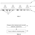
- FIG. 9 is a schematic structural view of a display panel according to an embodiment of the present disclosure. As illustrated in FIG. 9 , unlike the above embodiment, the reflective structure group 3 according to this embodiment is located on a side of the first substrate 1 facing away from the second substrate 2. The specific process of implementing the multiple visual fields of view for the display panel to display by using the reflective structure group 3 in this embodiment will not be described herein again.
- An embodiment of the present disclosure provides a display device including a display panel according to the above embodiment. Descriptions of the display panel may refer to the content in the foregoing embodiments and will not be described herein again.
- FIG. 10 is a flow chart illustrating a method of manufacturing a display panel.
- the method of manufacturing the display panel includes: steps S1-S2.
- a first substrate and a second substrate is prepared, respectively.
- One of the first substrate and the second substrate is an array substrate, and the other is an opposite substrate.
- the first substrate and the second substrate may be prepared by an existing manufacturing process for an array substrate and an existing manufacturing process for an opposite substrate.
- reflective structure groups are formed such that the reflective structure groups are located on a side of the first substrate facing the second substrate or distal to the second substrate, and each reflective structure group includes a plurality of reflective structures in one-to-one correspondence with the visual fields of view.
- each reflective structure faces the second substrate, and the reflective structure is configured to reflect the light from the second substrate in a predetermined direction to a corresponding visual field of view.
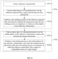
- FIG. 11 is a specific flow chart illustrating the step S2 of FIG. 10
- FIG. 12 is a schematic diagram illustrating a process of manufacturing a reflective structure group by using the flow chart illustrated in FIG. 11
- the step S2 includes: forming respective reflective structures in each reflective structure group, and each reflective structure includes a plurality of reflective substructures disposed along the first direction, and reflective surfaces of the respective reflective substructures located in a same reflective structure are disposed in parallel.
- the step of forming the respective reflective structures includes: steps S21a-S22a.
- an initial pattern of the reflective substructure is formed by a first patterning process, such that a shape of a longitudinal section of the initial pattern of the reflective substructure is a rectangle.
- the step S21a specifically includes: steps S211a and S212a.
- a reflective material film is formed.
- a reflective material film 8 is formed on the substrate 7 by an evaporation or vapor deposition process, as illustrated in Fig. 12A .
- the material of the reflective material film 8 is a metal material.
- an entire layer of a first photoresist is coated over the reflective material film, and then is exposed and developed.
- the reflective substructure finally formed must include a vertical plane perpendicular to the display panel and an inclined plane with a certain inclination angle with respect to the display panel.
- a forming region for the reflective substructure 12, an etching region reserved for the vertical plane 10, and an etching region reserved for the inclined plane 11 may be pre-designed, as illustrated in FIG. 12A .
- the forming region for the reflective substructure 12 is a region in which the reflective substructure is subsequently formed
- the etching region reserved for the vertical plane 10 is a set of all points distant from the bottom of the vertical plane of the reflective substructure in the first direction X by a distance less than or equal to a first predetermined distance a
- the etching region reserved for the inclined plane 11 is a set of all points distant from the bottom of the inclined plane of the reflective substructure in the first direction X by a distance less than or equal to a second predetermined distance b.
- the first predetermined distance a and the second predetermined distance b may be designed and adjusted according to actual needs.
- the first photoresist 9 located in the etching region reserved for the vertical plane 10 may be removed, and the first photoresist 9 located in the forming region for the reflective substructure 12 and the etching region reserved for the inclined plane 11 may be retained, as illustrated in FIG. 12(A) .
- a dry-etching process is performed on the reflective material film, and the retained first photoresist is stripped after the dry-etching process is completed, to obtain the initial pattern of the reflective substructure.
- a side of an initial pattern of the reflective substructure 81 formed by the dry-etching process must be perpendicular to the display panel (the longitudinal section of the initial pattern of the reflective substructure 81 is a rectangular). In this case, a side of the initial pattern of the reflective substructure 81 may function as the vertical plane of the reflective substructure finally formed.
- Fig. 12B illustrates the initial pattern of the reflective substructure with the first photoresist coated thereon, obtained after the dry-etching process is completed.
- Fig. 12C illustrates the initial pattern of the reflective substructure obtained by stripping the retained first photoresist after the dry-etching process is completed.
- the initial patterns of the reflective substructures in the respective reflective structures on the display panel may be manufactured simultaneously by one patterning process, to shorten the production cycle.
- the step of forming the respective reflective structures further includes: At the step S22a, the initial pattern of the reflective substructure is bevel-etched by a second patterning process to form the reflective substructure, such that a shape of longitudinal section of the reflective substructure is a right triangle.
- the step S22a specifically includes: steps S221a and S222a.
- an entire layer of a second photoresist is coated over the initial pattern of the reflective substructure, and is then exposed and developed.
- the second photoresist 13 located in the etching region reserved for the inclined plane 11 may be removed, and the second photoresist 13 located in the forming region for the reflective substructure 12 and the etching region reserved for the vertical plane 10 may be retained, as illustrated in FIG. 12D .
- the second photoresist 13 located in the etching region reserved for the vertical plane 10 completely covers the vertical plane of the finally formed reflective substructure (a side of the initial pattern of the reflective substructure 81) to avoid the vertical plane from being mis-etched in the subsequent wet-etching process.
- a wet-etching process is performed on the initial pattern of the reflective substructure, and the retained second photoresist is striped after the wet-etching process is completed, to obtain the reflective substructure with a shape of a longitudinal section of a right triangle.
- etching in the vertical direction Y but also etching in the horizontal direction (the first direction X) may be performed by the etching liquid.
- an inclined plane with a certain inclination angle may finally be obtained.
- Fig. 12E illustrates a reflective substructure with a second photoresist coated thereon, obtained after the wet-etching process is completed.
- Fig. 12F illustrates the reflective substructure obtained by stripping the retained second photoresist after the wet-etching process is completed.
- the vertical plane of the reflective substructure 311 may be obtained by the dry-etching process
- the inclined plane of the reflective substructure 311 may be obtained by the wet-etching process
- the inclination angle of the inclined plane may be controlled.
- step S22a only one inclined plane with a certain inclination angle may be obtained by one bevel-etching process (the step S221a and the step S222a). Inclined planes with different inclination angles may require multiple bevel-etching processes.
- a bevel-etching process the initial pattern of the reflective substructure that is not required to be etched and the reflective substructure that has been formed may be overlaid and protected by photoresist to avoid mis-etching.
- the region of the first photoresist retained after the development in the step S212a may be adjusted to retain the first photoresist located in the region reserved for the anti-crosstalk structure.
- the pattern of the anti-crosstalk structure may be obtained at the same time.
- FIG. 13 is a specific flow chart illustrating the step S2 of FIG. 10 and FIG. 14 is a schematic diagram illustrating a process of manufacturing a reflective structure group by using the flow chart illustrated in FIG. 13 .
- the step S2 includes: steps S21b to S23b.
- a photosensitive resin material film is formed.
- a photosensitive resin material film 14 is applied on the substrate 7, as illustrated in Fig. 14A .
- the photosensitive resin material film is exposed through a gray-scale mask plate, and the exposed photosensitive resin material film is developed to obtain a reflective substructure substrate model corresponding to the reflective substructure to be formed, such that the reflective substructure substrate model has a vertical plane and an inclined plane, and a shape of a longitudinal section of the reflective substructure substrate model is a right triangle.
- the photosensitive resin material film 14 is exposed through a gray-scale mask plate, and the gray-scale mask plate has light-transmissive regions with different light transmittances to expose different regions on the photosensitive resin material film to different degrees.
- a plurality of reflective substructure substrate models 15 with shapes of longitudinal sections of right triangles may be obtained, as illustrated in Fig. 14B .
- the inclination angle of the inclined plane of the reflective substructure substrate model 15 is the same as that of a corresponding reflective substructure.
- a reflective material film is formed on a surface of the reflective substructure substrate model such that the reflective substructure substrate model and the reflective material film covering a vertical plane and an inclined plane of the reflective substructure substrate model constitute the reflective substructure.
- a uniform reflective material film 16 is formed on the surface of the substrate obtained at the step S22b, as illustrated in Fig. 14C .
- the material of the reflective material film 16 is a metal material.
- the reflective substructure substrate model 15 and the reflective material film 16 covering the vertical plane and the inclined plane of the reflective substructure substrate model 15 constitute the reflective substructure 311. Since the shape of the longitudinal section of the reflective substructure substrate model 15 is a right triangle, the shape of the longitudinal section of the reflective substructure 311 is also a right triangle.
- the photosensitive resin material in a region corresponding to the anti-crosstalk structure to be formed may be completely or partially retained at the step S22b as an anti-crosstalk structure substrate model.
- the anti-crosstalk structure substrate model and a portion of the reflective material film on the upper surface of the anti-crosstalk structure substrate model constitute the anti-crosstalk structure.
- the reflective structure group when the reflective structure is located on a side of the first substrate facing the second substrate, the reflective structure group may be formed by using the first substrate as a substrate; when the reflective structure is located on a side of the first substrate distal to the second substrate, the reflective structure group may be manufactured on another substrate, and then be placed on the side of the first substrate distal to the second substrate, with the reflective surface of each reflective structure in the reflective structure group facing the second substrate.
Landscapes
- Physics & Mathematics (AREA)
- Nonlinear Science (AREA)
- General Physics & Mathematics (AREA)
- Optics & Photonics (AREA)
- Mathematical Physics (AREA)
- Crystallography & Structural Chemistry (AREA)
- Chemical & Material Sciences (AREA)
- Engineering & Computer Science (AREA)
- Health & Medical Sciences (AREA)
- Manufacturing & Machinery (AREA)
- Ophthalmology & Optometry (AREA)
- Mechanical Engineering (AREA)
- Devices For Indicating Variable Information By Combining Individual Elements (AREA)
- Liquid Crystal (AREA)
- Optical Elements Other Than Lenses (AREA)
Applications Claiming Priority (2)
| Application Number | Priority Date | Filing Date | Title |
|---|---|---|---|
| CN201710790365.2A CN109426026B (zh) | 2017-09-05 | 2017-09-05 | 显示面板及其制备方法和显示装置 |
| PCT/CN2018/093688 WO2019047601A1 (zh) | 2017-09-05 | 2018-06-29 | 显示面板及其制备方法和显示装置 |
Publications (3)
| Publication Number | Publication Date |
|---|---|
| EP3680707A1 EP3680707A1 (en) | 2020-07-15 |
| EP3680707A4 EP3680707A4 (en) | 2021-06-09 |
| EP3680707B1 true EP3680707B1 (en) | 2024-03-06 |
Family
ID=65513425
Family Applications (1)
| Application Number | Title | Priority Date | Filing Date |
|---|---|---|---|
| EP18853270.9A Active EP3680707B1 (en) | 2017-09-05 | 2018-06-29 | Display panel and preparation method therefor and display device thereof |
Country Status (4)
| Country | Link |
|---|---|
| US (1) | US11327359B2 (zh) |
| EP (1) | EP3680707B1 (zh) |
| CN (1) | CN109426026B (zh) |
| WO (1) | WO2019047601A1 (zh) |
Family Cites Families (15)
| Publication number | Priority date | Publication date | Assignee | Title |
|---|---|---|---|---|
| CN1311873A (zh) * | 1998-07-29 | 2001-09-05 | 松下电器产业株式会社 | 散射式显示器件及其驱动方法 |
| US6291146B1 (en) * | 1999-04-09 | 2001-09-18 | Industrial Technology Research Institute | Method for reforming a reflection-type light diffuser |
| GB2349237A (en) * | 1999-04-24 | 2000-10-25 | Sharp Kk | An optical element, method of manufacture thereof and a display device incorporating said element. |
| TW594218B (en) * | 2000-07-03 | 2004-06-21 | Alps Electric Co Ltd | Reflector and reflective liquid crystal display device |
| JP3960085B2 (ja) * | 2002-03-06 | 2007-08-15 | セイコーエプソン株式会社 | 立体画像表示装置 |
| JP2005135899A (ja) * | 2003-10-06 | 2005-05-26 | Omron Corp | 面光源装置及び表示装置 |
| JP4476137B2 (ja) * | 2005-02-28 | 2010-06-09 | セイコーエプソン株式会社 | 液晶装置および電子機器 |
| KR20080086118A (ko) | 2007-03-21 | 2008-09-25 | 엘지디스플레이 주식회사 | 반투과형 액정표시장치 및 그 제조방법 |
| CN101738760B (zh) * | 2008-11-11 | 2012-08-08 | 宏碁股份有限公司 | 像素结构、光学元件、液晶显示装置及其制造方法 |
| JP2011222237A (ja) | 2010-04-07 | 2011-11-04 | Sony Corp | 照明装置および表示装置 |
| CN103185293B (zh) * | 2011-12-29 | 2015-03-18 | 上海天马微电子有限公司 | 反射板、全反射3d显示装置 |
| CN102830537B (zh) * | 2012-08-31 | 2015-04-01 | 北京京东方光电科技有限公司 | 一种彩膜基板及其制造方法、显示装置 |
| CN103454807B (zh) | 2013-09-02 | 2016-07-27 | 京东方科技集团股份有限公司 | 阵列基板及其制作方法、3d显示装置 |
| CN105372824B (zh) | 2015-12-22 | 2017-12-29 | 苏州苏大维格光电科技股份有限公司 | 一种裸眼3d激光显示装置 |
| CN106937106A (zh) * | 2017-04-07 | 2017-07-07 | 京东方科技集团股份有限公司 | 反射式3d显示装置 |
-
2017
- 2017-09-05 CN CN201710790365.2A patent/CN109426026B/zh active Active
-
2018
- 2018-06-29 US US16/332,168 patent/US11327359B2/en active Active
- 2018-06-29 EP EP18853270.9A patent/EP3680707B1/en active Active
- 2018-06-29 WO PCT/CN2018/093688 patent/WO2019047601A1/zh unknown
Also Published As
| Publication number | Publication date |
|---|---|
| CN109426026B (zh) | 2022-08-23 |
| EP3680707A1 (en) | 2020-07-15 |
| EP3680707A4 (en) | 2021-06-09 |
| US11327359B2 (en) | 2022-05-10 |
| WO2019047601A1 (zh) | 2019-03-14 |
| CN109426026A (zh) | 2019-03-05 |
| US20210349347A1 (en) | 2021-11-11 |
Similar Documents
| Publication | Publication Date | Title |
|---|---|---|
| EP3365723B1 (en) | Method and system for performing sub-pixel compression in order to reduce moiré interference in a display system including multiple displays | |
| US9488879B2 (en) | Liquid crystal lens panel and display apparatus having the same | |
| KR101291860B1 (ko) | 2차원 영상 및 3차원 영상 디스플레이장치, 그 제조방법 | |
| US20150109666A1 (en) | Array substrate and manufacturing method thereof, 3d display device | |
| US8576141B2 (en) | Three-dimensional display device and image presentation method | |
| JPWO2014196125A1 (ja) | 画像表示装置及び液晶レンズ | |
| CN108605121B (zh) | 使用具有正方形元件轮廓的折射光束映射器减少自动立体显示器中的莫尔干涉的方法和系统 | |
| US10477196B2 (en) | Method and system using refractive bam mapper to reduce moire interference in a display system including multiple displays | |
| US11042068B2 (en) | Display substrate and manufacturing method thereof, display device | |
| JP2005266438A (ja) | 表示装置及びその製造方法 | |
| EP3680707B1 (en) | Display panel and preparation method therefor and display device thereof | |
| US10684491B2 (en) | Method and system using refractive beam mapper having square element profiles to reduce moire interference in a display system including multiple displays | |
| CN203422540U (zh) | 一种裸眼立体液晶显示系统 | |
| CN205787398U (zh) | 一种显示面板和显示设备 | |
| EP3622348B1 (en) | Method and system for reducing fresnel depolarization to improve image contrast in display system including multiple displays | |
| KR20120126562A (ko) | 영상 표시장치 | |
| CN202230254U (zh) | 偏振分光器件 | |
| CN108254934B (zh) | 显示装置 | |
| KR101313652B1 (ko) | 입체영상표시장치와 이의 제조방법 | |
| JP2002311419A (ja) | 液晶表示パネルの透明基板、液晶表示パネル及び立体視映像表示装置 | |
| CN114930234B (zh) | 显示面板及其制造方法、显示装置 | |
| KR101966726B1 (ko) | 영상 표시장치 | |
| KR101886304B1 (ko) | 영상 표시장치 및 그 제조 방법 | |
| KR101925413B1 (ko) | 영상 표시장치 및 그 제조 방법 | |
| CN111123548A (zh) | 一种裸眼3d电视的制作方法 |
Legal Events
| Date | Code | Title | Description |
|---|---|---|---|
| STAA | Information on the status of an ep patent application or granted ep patent |
Free format text: STATUS: THE INTERNATIONAL PUBLICATION HAS BEEN MADE |
|
| PUAI | Public reference made under article 153(3) epc to a published international application that has entered the european phase |
Free format text: ORIGINAL CODE: 0009012 |
|
| STAA | Information on the status of an ep patent application or granted ep patent |
Free format text: STATUS: REQUEST FOR EXAMINATION WAS MADE |
|
| 17P | Request for examination filed |
Effective date: 20190319 |
|
| AK | Designated contracting states |
Kind code of ref document: A1 Designated state(s): AL AT BE BG CH CY CZ DE DK EE ES FI FR GB GR HR HU IE IS IT LI LT LU LV MC MK MT NL NO PL PT RO RS SE SI SK SM TR |
|
| AX | Request for extension of the european patent |
Extension state: BA ME |
|
| DAV | Request for validation of the european patent (deleted) | ||
| DAX | Request for extension of the european patent (deleted) | ||
| A4 | Supplementary search report drawn up and despatched |
Effective date: 20210511 |
|
| RIC1 | Information provided on ipc code assigned before grant |
Ipc: G02F 1/1335 20060101AFI20210505BHEP Ipc: G02B 30/33 20200101ALI20210505BHEP Ipc: G02B 5/136 20060101ALI20210505BHEP Ipc: B29D 11/00 20060101ALN20210505BHEP Ipc: G02B 5/12 20060101ALN20210505BHEP Ipc: B29L 31/34 20060101ALN20210505BHEP Ipc: H04N 13/00 20180101ALN20210505BHEP |
|
| GRAP | Despatch of communication of intention to grant a patent |
Free format text: ORIGINAL CODE: EPIDOSNIGR1 |
|
| STAA | Information on the status of an ep patent application or granted ep patent |
Free format text: STATUS: GRANT OF PATENT IS INTENDED |
|
| RIC1 | Information provided on ipc code assigned before grant |
Ipc: H04N 13/00 20180101ALN20231025BHEP Ipc: B29L 31/34 20060101ALN20231025BHEP Ipc: G02B 5/12 20060101ALN20231025BHEP Ipc: B29D 11/00 20060101ALN20231025BHEP Ipc: G02B 5/136 20060101ALI20231025BHEP Ipc: G02B 30/33 20200101ALI20231025BHEP Ipc: G02F 1/1335 20060101AFI20231025BHEP |
|
| RIC1 | Information provided on ipc code assigned before grant |
Ipc: H04N 13/00 20180101ALN20231027BHEP Ipc: B29L 31/34 20060101ALN20231027BHEP Ipc: G02B 5/12 20060101ALN20231027BHEP Ipc: B29D 11/00 20060101ALN20231027BHEP Ipc: G02B 5/136 20060101ALI20231027BHEP Ipc: G02B 30/33 20200101ALI20231027BHEP Ipc: G02F 1/1335 20060101AFI20231027BHEP |
|
| INTG | Intention to grant announced |
Effective date: 20231115 |
|
| RAP3 | Party data changed (applicant data changed or rights of an application transferred) |
Owner name: HEFEI BOE OPTOELECTRONICS TECHNOLOGY CO., LTD. Owner name: BOE TECHNOLOGY GROUP CO., LTD. |
|
| GRAS | Grant fee paid |
Free format text: ORIGINAL CODE: EPIDOSNIGR3 |
|
| GRAA | (expected) grant |
Free format text: ORIGINAL CODE: 0009210 |
|
| STAA | Information on the status of an ep patent application or granted ep patent |
Free format text: STATUS: THE PATENT HAS BEEN GRANTED |
|
| AK | Designated contracting states |
Kind code of ref document: B1 Designated state(s): AL AT BE BG CH CY CZ DE DK EE ES FI FR GB GR HR HU IE IS IT LI LT LU LV MC MK MT NL NO PL PT RO RS SE SI SK SM TR |
|
| REG | Reference to a national code |
Ref country code: GB Ref legal event code: FG4D |
|
| REG | Reference to a national code |
Ref country code: CH Ref legal event code: EP |
|
| REG | Reference to a national code |
Ref country code: IE Ref legal event code: FG4D |
|
| REG | Reference to a national code |
Ref country code: DE Ref legal event code: R096 Ref document number: 602018066344 Country of ref document: DE |
|
| REG | Reference to a national code |
Ref country code: LT Ref legal event code: MG9D |
|
| PG25 | Lapsed in a contracting state [announced via postgrant information from national office to epo] |
Ref country code: LT Free format text: LAPSE BECAUSE OF FAILURE TO SUBMIT A TRANSLATION OF THE DESCRIPTION OR TO PAY THE FEE WITHIN THE PRESCRIBED TIME-LIMIT Effective date: 20240306 |
|
| PGFP | Annual fee paid to national office [announced via postgrant information from national office to epo] |
Ref country code: DE Payment date: 20240617 Year of fee payment: 7 |
|
| REG | Reference to a national code |
Ref country code: NL Ref legal event code: MP Effective date: 20240306 |
|
| PG25 | Lapsed in a contracting state [announced via postgrant information from national office to epo] |
Ref country code: GR Free format text: LAPSE BECAUSE OF FAILURE TO SUBMIT A TRANSLATION OF THE DESCRIPTION OR TO PAY THE FEE WITHIN THE PRESCRIBED TIME-LIMIT Effective date: 20240607 |
|
| PG25 | Lapsed in a contracting state [announced via postgrant information from national office to epo] |
Ref country code: RS Free format text: LAPSE BECAUSE OF FAILURE TO SUBMIT A TRANSLATION OF THE DESCRIPTION OR TO PAY THE FEE WITHIN THE PRESCRIBED TIME-LIMIT Effective date: 20240606 Ref country code: HR Free format text: LAPSE BECAUSE OF FAILURE TO SUBMIT A TRANSLATION OF THE DESCRIPTION OR TO PAY THE FEE WITHIN THE PRESCRIBED TIME-LIMIT Effective date: 20240306 |
|
| PG25 | Lapsed in a contracting state [announced via postgrant information from national office to epo] |
Ref country code: ES Free format text: LAPSE BECAUSE OF FAILURE TO SUBMIT A TRANSLATION OF THE DESCRIPTION OR TO PAY THE FEE WITHIN THE PRESCRIBED TIME-LIMIT Effective date: 20240306 |
|
| PG25 | Lapsed in a contracting state [announced via postgrant information from national office to epo] |
Ref country code: RS Free format text: LAPSE BECAUSE OF FAILURE TO SUBMIT A TRANSLATION OF THE DESCRIPTION OR TO PAY THE FEE WITHIN THE PRESCRIBED TIME-LIMIT Effective date: 20240606 Ref country code: NO Free format text: LAPSE BECAUSE OF FAILURE TO SUBMIT A TRANSLATION OF THE DESCRIPTION OR TO PAY THE FEE WITHIN THE PRESCRIBED TIME-LIMIT Effective date: 20240606 Ref country code: LT Free format text: LAPSE BECAUSE OF FAILURE TO SUBMIT A TRANSLATION OF THE DESCRIPTION OR TO PAY THE FEE WITHIN THE PRESCRIBED TIME-LIMIT Effective date: 20240306 Ref country code: HR Free format text: LAPSE BECAUSE OF FAILURE TO SUBMIT A TRANSLATION OF THE DESCRIPTION OR TO PAY THE FEE WITHIN THE PRESCRIBED TIME-LIMIT Effective date: 20240306 Ref country code: GR Free format text: LAPSE BECAUSE OF FAILURE TO SUBMIT A TRANSLATION OF THE DESCRIPTION OR TO PAY THE FEE WITHIN THE PRESCRIBED TIME-LIMIT Effective date: 20240607 Ref country code: FI Free format text: LAPSE BECAUSE OF FAILURE TO SUBMIT A TRANSLATION OF THE DESCRIPTION OR TO PAY THE FEE WITHIN THE PRESCRIBED TIME-LIMIT Effective date: 20240306 Ref country code: ES Free format text: LAPSE BECAUSE OF FAILURE TO SUBMIT A TRANSLATION OF THE DESCRIPTION OR TO PAY THE FEE WITHIN THE PRESCRIBED TIME-LIMIT Effective date: 20240306 Ref country code: BG Free format text: LAPSE BECAUSE OF FAILURE TO SUBMIT A TRANSLATION OF THE DESCRIPTION OR TO PAY THE FEE WITHIN THE PRESCRIBED TIME-LIMIT Effective date: 20240306 |
|
| REG | Reference to a national code |
Ref country code: AT Ref legal event code: MK05 Ref document number: 1664115 Country of ref document: AT Kind code of ref document: T Effective date: 20240306 |
|
| PG25 | Lapsed in a contracting state [announced via postgrant information from national office to epo] |
Ref country code: SE Free format text: LAPSE BECAUSE OF FAILURE TO SUBMIT A TRANSLATION OF THE DESCRIPTION OR TO PAY THE FEE WITHIN THE PRESCRIBED TIME-LIMIT Effective date: 20240306 Ref country code: LV Free format text: LAPSE BECAUSE OF FAILURE TO SUBMIT A TRANSLATION OF THE DESCRIPTION OR TO PAY THE FEE WITHIN THE PRESCRIBED TIME-LIMIT Effective date: 20240306 |
|
| PG25 | Lapsed in a contracting state [announced via postgrant information from national office to epo] |
Ref country code: NL Free format text: LAPSE BECAUSE OF FAILURE TO SUBMIT A TRANSLATION OF THE DESCRIPTION OR TO PAY THE FEE WITHIN THE PRESCRIBED TIME-LIMIT Effective date: 20240306 |