EP3679649B1 - Capteur microélectronique pour authentification biométrique - Google Patents
Capteur microélectronique pour authentification biométrique Download PDFInfo
- Publication number
- EP3679649B1 EP3679649B1 EP18796102.4A EP18796102A EP3679649B1 EP 3679649 B1 EP3679649 B1 EP 3679649B1 EP 18796102 A EP18796102 A EP 18796102A EP 3679649 B1 EP3679649 B1 EP 3679649B1
- Authority
- EP
- European Patent Office
- Prior art keywords
- layer
- sensor
- transistor
- 2deg
- gan
- Prior art date
- Legal status (The legal status is an assumption and is not a legal conclusion. Google has not performed a legal analysis and makes no representation as to the accuracy of the status listed.)
- Active
Links
- 238000004377 microelectronic Methods 0.000 title claims description 30
- 229910002601 GaN Inorganic materials 0.000 claims description 96
- JMASRVWKEDWRBT-UHFFFAOYSA-N Gallium nitride Chemical compound [Ga]#N JMASRVWKEDWRBT-UHFFFAOYSA-N 0.000 claims description 96
- 230000004888 barrier function Effects 0.000 claims description 57
- 238000000034 method Methods 0.000 claims description 40
- 239000004065 semiconductor Substances 0.000 claims description 27
- 239000000463 material Substances 0.000 claims description 24
- 229910052751 metal Inorganic materials 0.000 claims description 22
- 239000002184 metal Substances 0.000 claims description 22
- 239000000758 substrate Substances 0.000 claims description 19
- 230000003746 surface roughness Effects 0.000 claims description 17
- 238000001465 metallisation Methods 0.000 claims description 15
- 230000005855 radiation Effects 0.000 claims description 15
- 238000012545 processing Methods 0.000 claims description 13
- 239000004047 hole gas Substances 0.000 claims description 11
- 230000005533 two-dimensional electron gas Effects 0.000 claims description 10
- 238000012544 monitoring process Methods 0.000 claims description 6
- 229910052782 aluminium Inorganic materials 0.000 claims description 5
- 238000006073 displacement reaction Methods 0.000 claims description 5
- 230000003321 amplification Effects 0.000 claims description 4
- 230000007274 generation of a signal involved in cell-cell signaling Effects 0.000 claims description 4
- 238000003199 nucleic acid amplification method Methods 0.000 claims description 4
- 239000004038 photonic crystal Substances 0.000 claims description 4
- 238000003860 storage Methods 0.000 claims description 4
- 239000004411 aluminium Substances 0.000 claims description 3
- XAGFODPZIPBFFR-UHFFFAOYSA-N aluminium Chemical compound [Al] XAGFODPZIPBFFR-UHFFFAOYSA-N 0.000 claims description 3
- 230000000004 hemodynamic effect Effects 0.000 claims description 3
- 208000032140 Sleepiness Diseases 0.000 claims description 2
- 206010041349 Somnolence Diseases 0.000 claims description 2
- 230000003213 activating effect Effects 0.000 claims description 2
- 230000037321 sleepiness Effects 0.000 claims description 2
- 230000002463 transducing effect Effects 0.000 claims description 2
- 206010029216 Nervousness Diseases 0.000 claims 1
- 230000001939 inductive effect Effects 0.000 claims 1
- 230000003867 tiredness Effects 0.000 claims 1
- 208000016255 tiredness Diseases 0.000 claims 1
- 239000010410 layer Substances 0.000 description 224
- 108091006146 Channels Proteins 0.000 description 80
- 238000004519 manufacturing process Methods 0.000 description 19
- 210000004243 sweat Anatomy 0.000 description 19
- 230000015572 biosynthetic process Effects 0.000 description 14
- 230000008569 process Effects 0.000 description 13
- MWUXSHHQAYIFBG-UHFFFAOYSA-N Nitric oxide Chemical compound O=[N] MWUXSHHQAYIFBG-UHFFFAOYSA-N 0.000 description 12
- 238000001020 plasma etching Methods 0.000 description 12
- 210000003491 skin Anatomy 0.000 description 12
- 230000005684 electric field Effects 0.000 description 11
- 230000000694 effects Effects 0.000 description 10
- 239000010931 gold Substances 0.000 description 10
- 230000035945 sensitivity Effects 0.000 description 10
- 238000004088 simulation Methods 0.000 description 10
- 238000001228 spectrum Methods 0.000 description 10
- 238000005468 ion implantation Methods 0.000 description 9
- 238000009826 distribution Methods 0.000 description 8
- 229910052737 gold Inorganic materials 0.000 description 8
- 238000000231 atomic layer deposition Methods 0.000 description 7
- 230000008878 coupling Effects 0.000 description 7
- 238000010168 coupling process Methods 0.000 description 7
- 238000005859 coupling reaction Methods 0.000 description 7
- 230000006870 function Effects 0.000 description 7
- 230000004044 response Effects 0.000 description 7
- 230000003595 spectral effect Effects 0.000 description 7
- 229910001218 Gallium arsenide Inorganic materials 0.000 description 6
- 238000005516 engineering process Methods 0.000 description 6
- 238000005530 etching Methods 0.000 description 6
- 239000007789 gas Substances 0.000 description 6
- 238000004611 spectroscopical analysis Methods 0.000 description 6
- 238000004458 analytical method Methods 0.000 description 5
- 125000004429 atom Chemical group 0.000 description 5
- 239000013078 crystal Substances 0.000 description 5
- 230000008901 benefit Effects 0.000 description 4
- 238000004891 communication Methods 0.000 description 4
- 230000007423 decrease Effects 0.000 description 4
- 230000001419 dependent effect Effects 0.000 description 4
- 238000000151 deposition Methods 0.000 description 4
- 238000001514 detection method Methods 0.000 description 4
- 230000005669 field effect Effects 0.000 description 4
- 238000001459 lithography Methods 0.000 description 4
- 238000000623 plasma-assisted chemical vapour deposition Methods 0.000 description 4
- 230000036962 time dependent Effects 0.000 description 4
- 238000013459 approach Methods 0.000 description 3
- 230000006399 behavior Effects 0.000 description 3
- 239000006227 byproduct Substances 0.000 description 3
- 230000007547 defect Effects 0.000 description 3
- 230000008021 deposition Effects 0.000 description 3
- 238000011161 development Methods 0.000 description 3
- 230000001965 increasing effect Effects 0.000 description 3
- 238000005259 measurement Methods 0.000 description 3
- 230000007246 mechanism Effects 0.000 description 3
- 150000004767 nitrides Chemical class 0.000 description 3
- 125000004433 nitrogen atom Chemical group N* 0.000 description 3
- 238000005334 plasma enhanced chemical vapour deposition Methods 0.000 description 3
- 238000010926 purge Methods 0.000 description 3
- 238000012546 transfer Methods 0.000 description 3
- 229910000980 Aluminium gallium arsenide Inorganic materials 0.000 description 2
- KRHYYFGTRYWZRS-UHFFFAOYSA-N Fluorane Chemical compound F KRHYYFGTRYWZRS-UHFFFAOYSA-N 0.000 description 2
- WQZGKKKJIJFFOK-GASJEMHNSA-N Glucose Natural products OC[C@H]1OC(O)[C@H](O)[C@@H](O)[C@@H]1O WQZGKKKJIJFFOK-GASJEMHNSA-N 0.000 description 2
- 229910002244 LaAlO3 Inorganic materials 0.000 description 2
- 229910002370 SrTiO3 Inorganic materials 0.000 description 2
- 238000009825 accumulation Methods 0.000 description 2
- 238000010009 beating Methods 0.000 description 2
- 230000009286 beneficial effect Effects 0.000 description 2
- 239000012620 biological material Substances 0.000 description 2
- 239000008280 blood Substances 0.000 description 2
- 210000004369 blood Anatomy 0.000 description 2
- 239000000969 carrier Substances 0.000 description 2
- 230000008859 change Effects 0.000 description 2
- 239000002800 charge carrier Substances 0.000 description 2
- 238000006243 chemical reaction Methods 0.000 description 2
- 229910052804 chromium Inorganic materials 0.000 description 2
- 238000000708 deep reactive-ion etching Methods 0.000 description 2
- 238000003795 desorption Methods 0.000 description 2
- 210000002615 epidermis Anatomy 0.000 description 2
- 238000002474 experimental method Methods 0.000 description 2
- 239000008103 glucose Substances 0.000 description 2
- 238000003384 imaging method Methods 0.000 description 2
- 238000002847 impedance measurement Methods 0.000 description 2
- 239000012535 impurity Substances 0.000 description 2
- 238000009616 inductively coupled plasma Methods 0.000 description 2
- 230000003993 interaction Effects 0.000 description 2
- 230000003340 mental effect Effects 0.000 description 2
- 150000002739 metals Chemical class 0.000 description 2
- 230000003287 optical effect Effects 0.000 description 2
- 238000002161 passivation Methods 0.000 description 2
- 238000009832 plasma treatment Methods 0.000 description 2
- 230000010287 polarization Effects 0.000 description 2
- 239000000376 reactant Substances 0.000 description 2
- HBMJWWWQQXIZIP-UHFFFAOYSA-N silicon carbide Chemical compound [Si+]#[C-] HBMJWWWQQXIZIP-UHFFFAOYSA-N 0.000 description 2
- 229910010271 silicon carbide Inorganic materials 0.000 description 2
- 239000002356 single layer Substances 0.000 description 2
- 238000001179 sorption measurement Methods 0.000 description 2
- 239000000126 substance Substances 0.000 description 2
- 210000000707 wrist Anatomy 0.000 description 2
- 229910052984 zinc sulfide Inorganic materials 0.000 description 2
- 229910017083 AlN Inorganic materials 0.000 description 1
- PIGFYZPCRLYGLF-UHFFFAOYSA-N Aluminum nitride Chemical compound [Al]#N PIGFYZPCRLYGLF-UHFFFAOYSA-N 0.000 description 1
- 230000005457 Black-body radiation Effects 0.000 description 1
- 238000009623 Bosch process Methods 0.000 description 1
- YCKRFDGAMUMZLT-UHFFFAOYSA-N Fluorine atom Chemical compound [F] YCKRFDGAMUMZLT-UHFFFAOYSA-N 0.000 description 1
- XUIMIQQOPSSXEZ-UHFFFAOYSA-N Silicon Chemical compound [Si] XUIMIQQOPSSXEZ-UHFFFAOYSA-N 0.000 description 1
- 208000032364 Undersensing Diseases 0.000 description 1
- 238000010521 absorption reaction Methods 0.000 description 1
- PNEYBMLMFCGWSK-UHFFFAOYSA-N aluminium oxide Inorganic materials [O-2].[O-2].[O-2].[Al+3].[Al+3] PNEYBMLMFCGWSK-UHFFFAOYSA-N 0.000 description 1
- 238000000089 atomic force micrograph Methods 0.000 description 1
- QVGXLLKOCUKJST-UHFFFAOYSA-N atomic oxygen Chemical compound [O] QVGXLLKOCUKJST-UHFFFAOYSA-N 0.000 description 1
- 239000012159 carrier gas Substances 0.000 description 1
- 238000012512 characterization method Methods 0.000 description 1
- 238000005229 chemical vapour deposition Methods 0.000 description 1
- 238000002983 circular dichroism Methods 0.000 description 1
- 238000010367 cloning Methods 0.000 description 1
- 230000000052 comparative effect Effects 0.000 description 1
- 239000012141 concentrate Substances 0.000 description 1
- 239000004020 conductor Substances 0.000 description 1
- 238000010276 construction Methods 0.000 description 1
- 210000004087 cornea Anatomy 0.000 description 1
- 230000001351 cycling effect Effects 0.000 description 1
- 210000004207 dermis Anatomy 0.000 description 1
- 230000006866 deterioration Effects 0.000 description 1
- 229940079593 drug Drugs 0.000 description 1
- 239000003814 drug Substances 0.000 description 1
- 238000001312 dry etching Methods 0.000 description 1
- 239000003792 electrolyte Substances 0.000 description 1
- 230000005672 electromagnetic field Effects 0.000 description 1
- 230000002708 enhancing effect Effects 0.000 description 1
- 230000005284 excitation Effects 0.000 description 1
- 238000011049 filling Methods 0.000 description 1
- 229910052731 fluorine Inorganic materials 0.000 description 1
- 239000011737 fluorine Substances 0.000 description 1
- 229910052733 gallium Inorganic materials 0.000 description 1
- PCHJSUWPFVWCPO-UHFFFAOYSA-N gold Chemical compound [Au] PCHJSUWPFVWCPO-UHFFFAOYSA-N 0.000 description 1
- 210000004247 hand Anatomy 0.000 description 1
- 239000001257 hydrogen Substances 0.000 description 1
- 229910052739 hydrogen Inorganic materials 0.000 description 1
- 229910000040 hydrogen fluoride Inorganic materials 0.000 description 1
- 238000010348 incorporation Methods 0.000 description 1
- 150000002500 ions Chemical class 0.000 description 1
- 239000007791 liquid phase Substances 0.000 description 1
- 230000033001 locomotion Effects 0.000 description 1
- 210000004072 lung Anatomy 0.000 description 1
- 238000013507 mapping Methods 0.000 description 1
- 238000002483 medication Methods 0.000 description 1
- 239000012528 membrane Substances 0.000 description 1
- 238000002488 metal-organic chemical vapour deposition Methods 0.000 description 1
- 238000012986 modification Methods 0.000 description 1
- 230000004048 modification Effects 0.000 description 1
- 230000007935 neutral effect Effects 0.000 description 1
- 229910052756 noble gas Inorganic materials 0.000 description 1
- 239000001301 oxygen Substances 0.000 description 1
- 229910052760 oxygen Inorganic materials 0.000 description 1
- 238000005240 physical vapour deposition Methods 0.000 description 1
- 238000000678 plasma activation Methods 0.000 description 1
- 230000001902 propagating effect Effects 0.000 description 1
- 230000006798 recombination Effects 0.000 description 1
- 238000005215 recombination Methods 0.000 description 1
- 238000006479 redox reaction Methods 0.000 description 1
- 230000009467 reduction Effects 0.000 description 1
- 230000001105 regulatory effect Effects 0.000 description 1
- 238000011160 research Methods 0.000 description 1
- 230000002441 reversible effect Effects 0.000 description 1
- 230000001020 rhythmical effect Effects 0.000 description 1
- 229910052594 sapphire Inorganic materials 0.000 description 1
- 239000010980 sapphire Substances 0.000 description 1
- 238000007493 shaping process Methods 0.000 description 1
- 229910052710 silicon Inorganic materials 0.000 description 1
- 239000010703 silicon Substances 0.000 description 1
- 238000004528 spin coating Methods 0.000 description 1
- 230000002269 spontaneous effect Effects 0.000 description 1
- 238000006467 substitution reaction Methods 0.000 description 1
- 239000002344 surface layer Substances 0.000 description 1
- 238000010301 surface-oxidation reaction Methods 0.000 description 1
- 230000035900 sweating Effects 0.000 description 1
- 238000012360 testing method Methods 0.000 description 1
- 229910052721 tungsten Inorganic materials 0.000 description 1
- 238000002460 vibrational spectroscopy Methods 0.000 description 1
- 238000001039 wet etching Methods 0.000 description 1
Images


Classifications
-
- A—HUMAN NECESSITIES
- A61—MEDICAL OR VETERINARY SCIENCE; HYGIENE
- A61B—DIAGNOSIS; SURGERY; IDENTIFICATION
- A61B5/00—Measuring for diagnostic purposes; Identification of persons
- A61B5/05—Detecting, measuring or recording for diagnosis by means of electric currents or magnetic fields; Measuring using microwaves or radio waves
- A61B5/0507—Detecting, measuring or recording for diagnosis by means of electric currents or magnetic fields; Measuring using microwaves or radio waves using microwaves or terahertz waves
-
- A—HUMAN NECESSITIES
- A61—MEDICAL OR VETERINARY SCIENCE; HYGIENE
- A61B—DIAGNOSIS; SURGERY; IDENTIFICATION
- A61B5/00—Measuring for diagnostic purposes; Identification of persons
- A61B5/0002—Remote monitoring of patients using telemetry, e.g. transmission of vital signals via a communication network
- A61B5/0015—Remote monitoring of patients using telemetry, e.g. transmission of vital signals via a communication network characterised by features of the telemetry system
- A61B5/0022—Monitoring a patient using a global network, e.g. telephone networks, internet
-
- A—HUMAN NECESSITIES
- A61—MEDICAL OR VETERINARY SCIENCE; HYGIENE
- A61B—DIAGNOSIS; SURGERY; IDENTIFICATION
- A61B5/00—Measuring for diagnostic purposes; Identification of persons
- A61B5/117—Identification of persons
-
- A—HUMAN NECESSITIES
- A61—MEDICAL OR VETERINARY SCIENCE; HYGIENE
- A61B—DIAGNOSIS; SURGERY; IDENTIFICATION
- A61B5/00—Measuring for diagnostic purposes; Identification of persons
- A61B5/68—Arrangements of detecting, measuring or recording means, e.g. sensors, in relation to patient
- A61B5/6801—Arrangements of detecting, measuring or recording means, e.g. sensors, in relation to patient specially adapted to be attached to or worn on the body surface
- A61B5/6802—Sensor mounted on worn items
-
- G—PHYSICS
- G16—INFORMATION AND COMMUNICATION TECHNOLOGY [ICT] SPECIALLY ADAPTED FOR SPECIFIC APPLICATION FIELDS
- G16H—HEALTHCARE INFORMATICS, i.e. INFORMATION AND COMMUNICATION TECHNOLOGY [ICT] SPECIALLY ADAPTED FOR THE HANDLING OR PROCESSING OF MEDICAL OR HEALTHCARE DATA
- G16H40/00—ICT specially adapted for the management or administration of healthcare resources or facilities; ICT specially adapted for the management or operation of medical equipment or devices
- G16H40/60—ICT specially adapted for the management or administration of healthcare resources or facilities; ICT specially adapted for the management or operation of medical equipment or devices for the operation of medical equipment or devices
- G16H40/67—ICT specially adapted for the management or administration of healthcare resources or facilities; ICT specially adapted for the management or operation of medical equipment or devices for the operation of medical equipment or devices for remote operation
-
- H—ELECTRICITY
- H01—ELECTRIC ELEMENTS
- H01L—SEMICONDUCTOR DEVICES NOT COVERED BY CLASS H10
- H01L31/00—Semiconductor devices sensitive to infrared radiation, light, electromagnetic radiation of shorter wavelength or corpuscular radiation and specially adapted either for the conversion of the energy of such radiation into electrical energy or for the control of electrical energy by such radiation; Processes or apparatus specially adapted for the manufacture or treatment thereof or of parts thereof; Details thereof
- H01L31/08—Semiconductor devices sensitive to infrared radiation, light, electromagnetic radiation of shorter wavelength or corpuscular radiation and specially adapted either for the conversion of the energy of such radiation into electrical energy or for the control of electrical energy by such radiation; Processes or apparatus specially adapted for the manufacture or treatment thereof or of parts thereof; Details thereof in which radiation controls flow of current through the device, e.g. photoresistors
- H01L31/10—Semiconductor devices sensitive to infrared radiation, light, electromagnetic radiation of shorter wavelength or corpuscular radiation and specially adapted either for the conversion of the energy of such radiation into electrical energy or for the control of electrical energy by such radiation; Processes or apparatus specially adapted for the manufacture or treatment thereof or of parts thereof; Details thereof in which radiation controls flow of current through the device, e.g. photoresistors characterised by potential barriers, e.g. phototransistors
- H01L31/101—Devices sensitive to infrared, visible or ultraviolet radiation
- H01L31/112—Devices sensitive to infrared, visible or ultraviolet radiation characterised by field-effect operation, e.g. junction field-effect phototransistor
-
- A—HUMAN NECESSITIES
- A61—MEDICAL OR VETERINARY SCIENCE; HYGIENE
- A61B—DIAGNOSIS; SURGERY; IDENTIFICATION
- A61B2562/00—Details of sensors; Constructional details of sensor housings or probes; Accessories for sensors
- A61B2562/02—Details of sensors specially adapted for in-vivo measurements
- A61B2562/0228—Microwave sensors
-
- A—HUMAN NECESSITIES
- A61—MEDICAL OR VETERINARY SCIENCE; HYGIENE
- A61B—DIAGNOSIS; SURGERY; IDENTIFICATION
- A61B2562/00—Details of sensors; Constructional details of sensor housings or probes; Accessories for sensors
- A61B2562/02—Details of sensors specially adapted for in-vivo measurements
- A61B2562/028—Microscale sensors, e.g. electromechanical sensors [MEMS]
-
- A—HUMAN NECESSITIES
- A61—MEDICAL OR VETERINARY SCIENCE; HYGIENE
- A61B—DIAGNOSIS; SURGERY; IDENTIFICATION
- A61B2562/00—Details of sensors; Constructional details of sensor housings or probes; Accessories for sensors
- A61B2562/04—Arrangements of multiple sensors of the same type
- A61B2562/043—Arrangements of multiple sensors of the same type in a linear array
-
- A—HUMAN NECESSITIES
- A61—MEDICAL OR VETERINARY SCIENCE; HYGIENE
- A61B—DIAGNOSIS; SURGERY; IDENTIFICATION
- A61B2562/00—Details of sensors; Constructional details of sensor housings or probes; Accessories for sensors
- A61B2562/12—Manufacturing methods specially adapted for producing sensors for in-vivo measurements
-
- H—ELECTRICITY
- H01—ELECTRIC ELEMENTS
- H01L—SEMICONDUCTOR DEVICES NOT COVERED BY CLASS H10
- H01L29/00—Semiconductor devices specially adapted for rectifying, amplifying, oscillating or switching and having potential barriers; Capacitors or resistors having potential barriers, e.g. a PN-junction depletion layer or carrier concentration layer; Details of semiconductor bodies or of electrodes thereof ; Multistep manufacturing processes therefor
- H01L29/40—Electrodes ; Multistep manufacturing processes therefor
- H01L29/41—Electrodes ; Multistep manufacturing processes therefor characterised by their shape, relative sizes or dispositions
- H01L29/423—Electrodes ; Multistep manufacturing processes therefor characterised by their shape, relative sizes or dispositions not carrying the current to be rectified, amplified or switched
- H01L29/42312—Gate electrodes for field effect devices
- H01L29/42316—Gate electrodes for field effect devices for field-effect transistors
-
- H—ELECTRICITY
- H01—ELECTRIC ELEMENTS
- H01L—SEMICONDUCTOR DEVICES NOT COVERED BY CLASS H10
- H01L29/00—Semiconductor devices specially adapted for rectifying, amplifying, oscillating or switching and having potential barriers; Capacitors or resistors having potential barriers, e.g. a PN-junction depletion layer or carrier concentration layer; Details of semiconductor bodies or of electrodes thereof ; Multistep manufacturing processes therefor
- H01L29/66—Types of semiconductor device ; Multistep manufacturing processes therefor
- H01L29/68—Types of semiconductor device ; Multistep manufacturing processes therefor controllable by only the electric current supplied, or only the electric potential applied, to an electrode which does not carry the current to be rectified, amplified or switched
- H01L29/76—Unipolar devices, e.g. field effect transistors
- H01L29/772—Field effect transistors
- H01L29/778—Field effect transistors with two-dimensional charge carrier gas channel, e.g. HEMT ; with two-dimensional charge-carrier layer formed at a heterojunction interface
- H01L29/7781—Field effect transistors with two-dimensional charge carrier gas channel, e.g. HEMT ; with two-dimensional charge-carrier layer formed at a heterojunction interface with inverted single heterostructure, i.e. with active layer formed on top of wide bandgap layer, e.g. IHEMT
-
- H—ELECTRICITY
- H01—ELECTRIC ELEMENTS
- H01L—SEMICONDUCTOR DEVICES NOT COVERED BY CLASS H10
- H01L29/00—Semiconductor devices specially adapted for rectifying, amplifying, oscillating or switching and having potential barriers; Capacitors or resistors having potential barriers, e.g. a PN-junction depletion layer or carrier concentration layer; Details of semiconductor bodies or of electrodes thereof ; Multistep manufacturing processes therefor
- H01L29/66—Types of semiconductor device ; Multistep manufacturing processes therefor
- H01L29/68—Types of semiconductor device ; Multistep manufacturing processes therefor controllable by only the electric current supplied, or only the electric potential applied, to an electrode which does not carry the current to be rectified, amplified or switched
- H01L29/76—Unipolar devices, e.g. field effect transistors
- H01L29/772—Field effect transistors
- H01L29/778—Field effect transistors with two-dimensional charge carrier gas channel, e.g. HEMT ; with two-dimensional charge-carrier layer formed at a heterojunction interface
- H01L29/7782—Field effect transistors with two-dimensional charge carrier gas channel, e.g. HEMT ; with two-dimensional charge-carrier layer formed at a heterojunction interface with confinement of carriers by at least two heterojunctions, e.g. DHHEMT, quantum well HEMT, DHMODFET
- H01L29/7783—Field effect transistors with two-dimensional charge carrier gas channel, e.g. HEMT ; with two-dimensional charge-carrier layer formed at a heterojunction interface with confinement of carriers by at least two heterojunctions, e.g. DHHEMT, quantum well HEMT, DHMODFET using III-V semiconductor material
-
- H—ELECTRICITY
- H01—ELECTRIC ELEMENTS
- H01L—SEMICONDUCTOR DEVICES NOT COVERED BY CLASS H10
- H01L29/00—Semiconductor devices specially adapted for rectifying, amplifying, oscillating or switching and having potential barriers; Capacitors or resistors having potential barriers, e.g. a PN-junction depletion layer or carrier concentration layer; Details of semiconductor bodies or of electrodes thereof ; Multistep manufacturing processes therefor
- H01L29/66—Types of semiconductor device ; Multistep manufacturing processes therefor
- H01L29/68—Types of semiconductor device ; Multistep manufacturing processes therefor controllable by only the electric current supplied, or only the electric potential applied, to an electrode which does not carry the current to be rectified, amplified or switched
- H01L29/76—Unipolar devices, e.g. field effect transistors
- H01L29/772—Field effect transistors
- H01L29/778—Field effect transistors with two-dimensional charge carrier gas channel, e.g. HEMT ; with two-dimensional charge-carrier layer formed at a heterojunction interface
- H01L29/7786—Field effect transistors with two-dimensional charge carrier gas channel, e.g. HEMT ; with two-dimensional charge-carrier layer formed at a heterojunction interface with direct single heterostructure, i.e. with wide bandgap layer formed on top of active layer, e.g. direct single heterostructure MIS-like HEMT
Definitions
- the present application relates to the field of microelectronic sensors based on high-electron-mobility transistors and their use in detection and continuous monitoring of electrical signals generated by a human body in a sub-terahertz range.
- the present application relates to the open-gate pseudo-conducting high-electron-mobility transistors (PC-HEMTs) and their use in biometric authentication.
- PC-HEMTs open-gate pseudo-conducting high-electron-mobility transistors
- biometric authentication systems nowadays used in smartphones, key locks, airport and high security locations where an extremely high level of authentication is required.
- Commercially available authentication systems may include a fingerprint ID sensor, an iris ID sensor or speech recognition.
- these systems proved to have a relatively low security level.
- a new type of the biometric authentication device by Bionym based on the electrocardiogram (ECG)
- ECG electrocardiogram
- This device called “Nymi”
- Nymi is capable of capturing a unique electrocardiographic waveform of a person, and further maps it to ECG patterns.
- Nymi is continuously worn as a bracelet or wristband on the user's wrist and uses learning algorithms to memorise the user's ECG patterns in order to increase the quality and authentication level of the user.
- WO 2012151680 by Bionym discloses a biometric sensor based on the analysis of the ECG signals used to authenticate one or more individuals. This sensor relies on authenticating identity by matching the overall shape of the user's ECG waveform (captured via an electrocardiogram sensor).
- the sensor by Bionym sustains authentication so long as the wearer keeps the wristband on.
- the user puts the wristband on and touches a topside sensor with one hand to complete an electrical loop with the bottom-side sensor touching their wrist. That generates the ECG data used to authenticate their identity, and the wristband transmits the ECG via Bluetooth to the corresponding registered app, on a smartphone or other external device in proximity to the user, to verify the wearer's identity.
- the biometric authentication devices such as Nymi, and similar ECG-based devices however have several drawbacks.
- Nymi needs to be worn at all times, in order to use the authentication system, which may be intrusive to some users.
- Nymi and similar ECG-based devices do not provide a single-contact point for simple authenticate of a user, and require the user to perform rather complex steps and procedures to authenticate themselves prior to each use, for example to use both hands to close a circuit and authenticate the user, the process each user must perform on a daily basis. Therefore, these technologies cannot be integrated directly into end-point devices, such as credit cards and mobile phones, for a single-point authentication.
- ECG-based sensors there are two major disadvantages of using the above ECG-based sensors.
- a high-electron mobility transistor is known from HAOWEN HOU ET AL: "A sub-terahertz broadband detector based on a GaN high-electron-mobility transistor with nanoantennas", APPLIED PHYSICS EXPRESS, vol. 10, no. 1 .
- terahertz (THz) radiation could be extremely important for research related to the life sciences because of the unique capability of these low energy electromagnetic waves to interact with vibrations of atoms within biological molecules to produce specific molecular fingerprints (see for example, Globus et al. in "Terahertz Fourier transform characterization of biological materials in a liquid phase", J. Physics D: Applied Physics, 39(15), 3405-3413 ).
- Sub-THz spectroscopy uses wavelengths beyond those traditionally used for chemical and biomolecular analysis.
- Biological materials have found to be active in the frequency range of 0.05-1 THz and above (the submillimetre-wavelength range, about 1.5 to 30 cm -1 ). These frequency and wavelength domains, the spectral range between the upper end of the radio frequencies and the lowest optical frequencies were named the 'Terahertz Gap', because so little was known about them and because of the absence of radiation sources and detectors.
- Sub-THz vibrational spectroscopy is based on the interaction of THz radiation with internal molecular vibrations of low energy.
- a majority of the THz experimental data have recently been reported on frequencies above 1 THz and for relatively small biological molecules that are often prepared in crystalline form (for example, Heilweil et al. (2008), "Terahertz Spectroscopy of Biomolecules", In Terahertz Spectroscopy, Taylor and Francis, London, 2008, Chapter 7, pp 269-297 ).
- Low energy THz radiation interacts with the low-frequency internal molecular motions (vibrations) involving the weakest hydrogen bonds (H-bonds) and other weak connections within molecules by exciting these vibrations.
- the width of individual spectral lines and the intensity of resonance features, which are observed in sub-THz spectroscopy, are very sensitive to the relaxation processes of atomic dynamics (displacements) within a molecule. Those relaxation processes determine the discriminative capabilities of sub-THz spectroscopy. Appropriate spectral resolution must be used in THz spectroscopy to be able to acquire qualitative as well as quantitative information used to identify the molecules that will, in turn, increase detection accuracy and selectivity.
- the spectral response obtained by their simulations coincided with the analytical prediction of antenna theory and supported the hypothesis that the sweat ducts can indeed be regarded as helical antennas.
- the magnitude of the spectral response was found to be dependent on the conductivity of sweat in these frequencies, but the analysis of the frequencies related to the antenna-like modes were found to be independent of this parameter.
- the performed simulations demonstrate that variations of the spectra are observed in the vicinity of the frequencies close to the predicted axial response mode of the sweat ducts (regarded as helical antennas) at approximately 380 GHz.
- the results clearly show that the structure of the sweat ducts plays a key role in the shaping of the reflected spectra.
- the coiled nature of the human sweat duct can lead to electromagnetic behaviour reminiscent of a helical antenna.
- the present inventors proposed that analysis of sweat using electrochemical devices on human skin may provide a new route for biometric authentication. Every individual has his/her own sub-THz spectra and his/her own sweat-duct spatial skin-surface pattern. Using this unique sub-THz-pattern, it might be possible to record the very unique spectra and spatial duct pattern from each individual and then to authenticate them with an unprecedented precision.
- the present application describes embodiments of a microelectronic sensor based on a combination of an open-gate pseudo-conducting high-electron mobility transistor (PC-HEMT) and Vivaldi antenna.
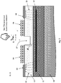
- the transistor comprises a substrate, on which a multilayer heterojunction structure is deposited.
- This hetero-junction structure may comprise at least one buffer layer and at least one barrier layer grown from III-V single-crystalline or polycrystalline semiconductor materials and stacked alternately.
- the III-V single-crystalline or polycrystalline semiconductor materials are GaN/AlGaN.
- a conducting channel comprising a two-dimensional electron gas (2DEG) or a two-dimensional hole gas (2DHG) is formed at the interface between the buffer and barrier layers and upon applying a bias to said transistor provides electron or hole current in the transistor between its source and drain electrodes.
- the heterojunction structure may be a three-layer structure consisting of two GaN layers and one AlGaN layer squeezed between said GaN layers like in a sandwich. This may lead to formation of the two-dimensional electron gas (2DEG) or two-dimensional hole gas (2DHG) in the top layer dependent on the polarity of the structure.
- An optional dielectric layer may be deposited on top of the heterojunction structure.
- the open gate area of the 2DEG/2DHG is formed between the source and drain areas as a result of recessing or growing of the top layer to a specific thickness.
- the source and drain non-ohmic (i.e. capacitively-coupled) contacts are connected to the 2DEG/2DHG channel and to electrical metallizations, the latter are placed on top of the sensor and connect it to an electric circuit of the sensor. Since the source and drain contacts are non-ohmic, the DC readout cannot be carried out. Instead, in order to electrically contact the 2DEG/2DHG channel underneath, about 5-20 nm bellow the metallizations, the AC readout or impedance measurements of the electric current flowing through the 2DEG/2DHG-channel must be performed. In this case, the capacitive coupling of the non-ohmic metal contacts with the 2DEG/2DHG channel is normally induced at the frequency higher than 30 kHz.
- the PC-HEMT multilayer heterojunction structure of the embodiments is grown from any available III-V single-crystalline or polycrystalline semiconductor materials, such as GaN/AlGaN, GaN/AIN, GaN/InN, GaN/InAlGaN, GaAs/AlGaAs, GaN/InAIN, InN/InAIN or LaAlO 3 /SrTiO 3 .
- the highest sensitivity of the sensor is achieved when thickness of the top recessed layer (GaN buffer layer or AlGaN barrier layer) in the open gate area between the source and drain contacts is 5-9 nm, preferably 6-7 nm, more preferably 6.2-6.4 nm.
- This recessed layer thickness corresponds to the pseudo-conducting current range between normally-on and normally-off operation mode of the 2DEG/2DHG conducting channel.
- surface roughness of the top recessed layer within the open gate area between the source and drain contacts has a roughness of about 0.2 nm or less, preferably 0.1 nm or less, more preferably 0.05 nm.
- the present application provides the sensing device suitable for use in biometric authentication.
- the term “about” is understood as within a range of normal tolerance in the art, for example within two standard deviations of the mean. In one embodiment, the term “about” means within 10% of the reported numerical value of the number with which it is being used, preferably within 5% of the reported numerical value. For example, the term “about” can be immediately understood as within 10%, 9%, 8%, 7%, 6%, 5%, 4%, 3%, 2%, 1%, 0.5%, 0.1%, 0.05%, or 0.01% of the stated value. In other embodiments, the term “about” can mean a higher tolerance of variation depending on for instance the experimental technique used. Said variations of a specified value are understood by the skilled person and are within the context of the present invention.
- a numerical range of "about 1 to about 5" should be interpreted to include not only the explicitly recited values of about 1 to about 5, but also include individual values and sub-ranges within the indicated range. Thus, included in this numerical range are individual values such as 2, 3, and 4 and sub-ranges, for example from 1-3, from 2-4, and from 3-5, as well as 1, 2, 3, 4, 5, or 6, individually. This same principle applies to ranges reciting only one numerical value as a minimum or a maximum. Unless otherwise clear from context, all numerical values provided herein are modified by the term “about”. Other similar terms, such as “substantially”, “generally”, “up to” and the like are to be construed as modifying a term or value such that it is not an absolute. Such terms will be defined by the circumstances and the terms that they modify as those terms are understood by those of skilled in the art. This includes, at very least, the degree of expected experimental error, technical error and instrumental error for a given experiment, technique or an instrument used to measure a value.
- the polarization doped high-electron-mobility transistor is a field effect transistor (FET) in which two layers of different bandgap and polarisation field are grown upon each other forming the heterojunction structure.
- This transistor is essentially based on at least two layers of III-V semiconductor materials, such as gallium nitride (GaN) and aluminium gallium nitride (AlGaN).
- GaN gallium nitride
- AlGaN aluminium gallium nitride
- channel electrons are confined in a quantum well in an infinitely narrow spatial region at the interface between the layers, these electrons are referred to as a two-dimensional electron gas (2DEG).
- 2DEG two-dimensional electron gas
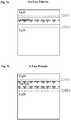
- Figs. 1a-1c schematically shows the quantum well at three different biasing conditions starting from the positive gate potential (V G ), much higher than the threshold voltage (V T ), and going down to the 0V gate potential and further to the negative values below the threshold voltage.
- V G is defined as a voltage, which is required to populate electrons at the interface between the GaN layer and the AlGaN layers, thereby creating conductivity of the 2DEG channel. Since the 2DEG channel electrons occupy energy levels below the Fermi level, the Fermi level in a quantum well is located above several energy levels when V G >> V T ( Fig. 1a ). This enables high population of channel electrons and consequently, high conductivity. The 2DEG channel is turned on in this case.
- HEMTs based on the layers of III-V semi-conductor materials have a negative value of V T , resulting in a "normally-on" operation mode at 0V gate potential. They are called “depletion-mode” semiconductor transistors and used in various power switching applications when the negative voltage must be applied on the gate in order to block the current. However, for safe operation at high voltage or high power density, in order to reduce the circuit complexity and eliminate standby power consumption, the transistors with "normally-off" characteristics are preferred. The high voltages and high switching speeds allow smaller, more efficient devices, such as home appliances, communications and automobiles to be manufactured. To control the density of electrons in the 2DEG channel and to switch the HEMT on and off, the voltage at the gate of the transistor is normally regulated.
- Burnham et al (2010) proposed normally-off structures of the recessed gate type.
- the AlGaN barrier layer is etched and the gate is brought closer to the interface between the AlGaN barrier layer and the GaN buffer layer.
- the V T increases.
- the normally-off operation of the 2DEG conducting channel is achieved once the depletion region reaches the interface and depletes the 2DEG channel at zero gate voltage.
- the major advantages of these structures are relatively lower power consumption, lower noise and simpler drive circuits. They are currently used, for example, in microwave and millimetre wave communications, imaging and radars.
- Chang et al (2009) proposed instead of etching the relatively thick barrier layer to approach the AlGaN/GaN interface, to use a very thin AlGaN barrier.
- This structure also achieves the normally-off operation of the 2DEG channel by approaching the gate towards the AlGaN/GaN interface.
- Chen et al (2010) proposed to use the fluorine-based plasma treatment method.
- many publications have adopted various methods to achieve normally-off devices with minimum impact on the drain current, they unfortunately sacrificed device turn-on performance.
- the present application describes embodiments of a microelectronic sensor based on a combination of an open-gate pseudo-conducting high-electron mobility transistor (PC-HEMT) and Vivaldi antenna installed in the open gate area of the transistor.
- PC-HEMT open-gate pseudo-conducting high-electron mobility transistor
- Vivaldi antenna installed in the open gate area of the transistor.
- the PC-HEMT of the present application capable of sensing sub-THz radiation produced by a body of the user, comprises:
- the functional basic topology of the microelectronic sensor of the present embodiments is schematically shown in Fig. 3 .
- the sensor detection principle is based on the field effect of electric current modulation in a DC-mode within the 2DEG/2DHG conducting channel (13) achieved by Vivaldi-shaped gate antenna (16).
- the Vivaldi-shaped gate antenna (16) is capable of strongly concentrating the electric field strength of sub-THz radiation in a very small area above the ultra charge-sensitive 2DEG/2DHG channel, thereby affecting its conductivity in the DC-mode by accumulation effect.
- the S11-S12 parameters of the PC-HEMT of the present embodiments however may also be measured at radio frequencies (RF) of 1 to 60 GHz using the 'beating' effect of sub-THz radiation.
- RF radio frequencies
- the transistor shown in Figs. 2 and 3 may further comprise a dielectric layer of 1-10 nm thickness.
- This dielectric layer may be deposited on top of the barrier layer (12).
- the Vivaldi antenna gate electrode made for example from gold, is then placed directly on the dielectric layer. This configuration prevents strong electrical leakage at the metal/top layer interface.
- the dielectric layer used for the device passivation may be made, for example, of SiO-SiN-SiO ("ONO") stack of 100-100-100 nm thickness or SiN-SiO-SiN (“NON”) stack having the same thicknesses. It may be deposited on top of the barrier layer by a method of plasma-enhanced chemical vapour deposition (PECVD), which is a stress-free deposition technique.
- PECVD plasma-enhanced chemical vapour deposition
- the electrical metallizations (14) connect the transistor to the electric circuit and allow the electric current to flow between non-ohmic contact areas (15) via the two-dimensional electron gas (2DEG) or two-dimensional hole gas (2DHG) channel (13).
- the metallizations (14) may be made of metal stacks, such as Cr/Au, Ti/Au, Ti/W, Cr/Al and Ti/Al.
- the Cr or Ti layers of the metal stack is, for example, of 5-10 nm thickness, while the second metal layer, such as Au, W and Al, is of 100-400 nm thickness.
- the metallizations (14) may be chosen according to the established technology and assembly line at a particular clean room fabrication facility.
- substrate layer (10) may be composed, for example, of sapphire, silicon, silicon carbide, gallium nitride or aluminium nitride.
- the hetero-junction structure (11, 12) may be deposited on the substrate layer (10), for example, by a method of metalorganic chemical vapour deposition (MOCVD), thereby forming the pseudo-conducting 2DEG or 2DHG channel (13) in the close proximity to the interface between the buffer layer (11) and the barrier layer (12).
- the barrier layer (12) then may be either recessed or grown in the recessed area (17) as a very thin layer between the source and drain contact areas (15).
- the 2DEG or 2DHG channel (13) formed near the interface between the buffer layer (11) and the barrier layer (12) serves as a main sensitive element of the transistor reacting to a surface charge and potential.
- the 2DEG or 2DHG channel (13) is configured to interact with very small variations in surface or proximal charge or changes of electrical field on the top layer/Vivaldi antenna gate interface interacting with the donor-like surface trap states of the barrier layer. This will be discussed below in detail.
- 2DEG two-dimensional electron gas
- the two-dimensional hole gas may also be a possible current carrier in a specific heterojunction structure. Therefore, the term “2DEG” may be equally replaced with the term “2DHG” without reference to any particular PC-HEMT configuration.
- the PC-HEMT multilayer heterojunction structure of the embodiments is grown from any available III-V single-crystalline or polycrystalline semiconductor materials, such as GaN/AlGaN, GaN/AIN, GaN/InAlGaN, GaN/InAIN, GaN/InN, GaAs/AlGaAs, InN/InAIN or LaAlO 3 /SrTiO 3 .
- the highest sensitivity of the sensor is achieved when thickness of the top recessed layer (GaN or AlGaN) in the open gate area between the source and drain contacts is 5-9 nm, preferably 6-7 nm, more preferably 6.2-6.4 nm.
- the sensor exhibits its highest sensitivity when surface roughness of the top recessed layer is about 0.2 nm or less, preferably 0.1 nm or less, more preferably 0.05 nm.
- the top layer recessed in the open gate area to 5-9 nm must be optimised for significantly enhancing sensitivity of the sensor.
- This specific thickness of the top layer was surprisingly found to correspond to the "pseudo-conducting" current range between normally-on and normally-off operation modes of the 2DEG channel and requires further explanation.
- "Pseudo-conducting" (to distinguish from normally-conducting) current range of the 2DEG channel is defined as an operation range of the channel between its normally-on and normally-off operation modes.
- Trap states are states in the band-gap of a semiconductor which trap a carrier until it recombines.
- Surface states are states caused by surface reconstruction of the local crystal due to surface tension caused by some crystal defects, dislocations, or the presence of impurities. Such surface reconstruction often creates “surface trap states” corresponding to a surface recombination velocity.
- Classification of the surface trap states depends on the relative position of their energy level inside the band gap.
- the surface trap states with energy above the Fermi level are acceptor-like, attaining negative charge when occupied.
- the surface trap states with energy below the Fermi level are donor-like, positively charged when empty and neutral when occupied.
- These donor-like surface trap states are considered to be the source of electrons in the formation of the 2DEG channel. They may possess a wide distribution of ionization energies within the band gap and are caused by redox reactions, dangling bonds and vacancies in the surface layer. A balance always exists between the 2DEG channel density and the number of ionised surface donors which is governed by charge neutrality and continuity of the electric field at the interfaces.
- the donor-like surface traps at the surface of the top layer are one of the most important sources of the 2DEG in the channel.
- the surface trap state In a relatively thin top layer, the surface trap state is below the Fermi level. However, as the top layer thickness increases, the energy of the surface trap state approaches the Fermi energy until it coincides with it. The thickness of the top layer corresponding to such situation is defined as "critical". At this point, electrons filling the surface trap state are pulled to the channel by the strong polarisation-induced electric field found in the top layer to form the 2DEG instantly.
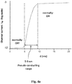
- Fig. 4a shows the dependence of the source-drain current (a charge carrier density) on the recessed AlGaN layer thickness.
- transistors that have a thickness of the top layer larger than 9 nm form normally-on 2DEG channels.
- a thin sheet of charges is induced at the top and bottom of the interfaces of the top layer.
- a high electric field is induced in the top layer, and surface donor states at the top interface start donating electrons to form the 2DEG channel at the proximity of the hetero-junction interface without the application of a gate bias.
- the transistors that have a thickness of the top layer lower than about 5 nm act constitute normally-off devices.
- Energy equilibrium between the donor surface trap states and AlGaN tunnel barrier leads to the 2DEG formation (charge neutrality combined with the lowest energy level) at the conduction band discontinuity.
- decrease in the thickness of the AlGaN layer results in increase of the energy barrier.
- the ionisable donor-like surface trap states which are responsible for electron tunnelling from the surface to 2DEG, drift bellow the Fermi level, thereby minimizing the electron supply to the 2DEG channel.
- Fig. 4b the recess of the AlGaN layer from 9 nm to 5 nm leads to huge drop in conductivity of the two-dimensional electron gas for six orders of magnitude.
- the mechanism of the 2DEG depletion based on recessing the top layer is strongly dependent on the donor-like surface trap states (or total surface charge). As the thickness of the top layer decreases, less additional external charge is needed to apply to the top layer surface in order to deplete the 2DEG channel.
- There is a critical (smallest) barrier thickness when the 2DEG channel is mostly depleted but still highly conductive due to a combination of the energy barrier and the donor surface trap states energy. At this critical thickness, even the smallest energy shift at the surface via any external influence, for example an acoustic wave propagating along the surface, leads immediately to the very strong 2DEG depletion.
- the surface of the top layer at this critical thickness is extremely sensitive to any smallest change in the electrical field of the surroundings.
- the recess of the top layer from 9 nm down to 5 nm significantly reduced the 2DEG density, brought the sensor to the "near threshold" operation and resulted in highly increased surface charge sensitivity.
- the specific 5-9 nm thickness of the top layer is actually responsible for the pseudo-conducting behaviour of the 2DEG channel and gives the sensor an enormous sensitivity.
- the top layer is recessed to this specific thickness after subjecting to short plasma activation by an ultra-low damage reactive-ion etching technique using inductively-coupled plasma (ICP) with a narrow plasma-ion energy distribution.
- ICP inductively-coupled plasma
- Such short plasma treatment allows much lower roughness of the surface, which is a function of the semiconductor vertical damage depth during the plasma etching process.
- Such low surface roughness (about 0.2 nm and less) can be achieved only via this ICP-RIE ultra low damage etching process with a narrow plasma-ion energy distribution, and this inherently results in a very low vertical damage depth to the top layer, which allows the minimal surface scattering and minimal surface states-2DEG channel interaction with the maximum signal-to-noise ratio of the sensor.
- the depth effect of the vertical sub-nanometre damage to the top recessed layer due to an ultra-low damage ICP-RIE etching process with a very narrow plasma-ion energy distribution, is the only way to optimally achieve the required sub-nanometre roughness of the semiconductor surface. This inherently results in an adjustable pseudo-conductive working point with the highest charge sensitivity ever possible. This depth effect is always inherent to the sub-nanometre roughness of the semiconductor surface, which was measured using AFM (atomic force microscope).
- roughness of the top layer surface is another very important parameter that has not been previously disclosed. It has been surprisingly found that the roughness of the top layer surface (in the open gate sensitive area) bellow 0.2 nm prevents scattering of the donor-like surface trap states. Thus, combination of these two features: 5-9 nm thickness of the top layer in the open gate area and strongly reduced roughness of its surface (bellow 0.2 nm) make the sensor incredibly sensitive.
- the method for manufacturing of the PC-HEMTs of the present invention comprises the following steps:
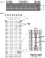
- Figs. 5a-5c showing the sensor, which is obtained in Step 4 of the 2DEG-channel pattering.
- the lithography of the sensor was performed with AZ 4533, which is a positive thick resist having optimised adhesion for common wet etching.
- the lithographic resist film thickness obtained at 7000-rpm spin speed and at 100° C for 1 min was 3 ⁇ m.
- the formed 2DEG channel (13) is approximately 2-3 ⁇ m wide.
- the overall exposure time was 9 sec, followed by 5-min development in MIF726 developer.
- Fig. 5d-5e show the mask and corresponding lithographic image, respectively, of the sensor layout of the present invention.
- Fig. 5f demonstrates the high alignment precision of ⁇ 2- ⁇ m on 25 x 25 mm 2 samples in the lithography of the sensor layout of the present invention.
- Fig. 5g shows the lithographic images of the multichannel samples.
- Fig. 5h shows the fixed sensor chip sample on the Si-GaN/AlGaN wafer, which contains approximately 30-32 sensors with 4-8 channels on each sample and prepared for ion implantation.
- Fig. 5i shows the obtained lithographic image of the present sensor layout with the AZ4533 resist after development, prepared for ion implantation.
- 5j shows the 2DEG channels (dark) patterned by ion-implantation after the resist removal.
- the argon-ion implantation was conducted with 20 keV and 30 keV energies and with an exemplary dose of 2.5e 13 /cm 2 and a 7° tilt angle.
- AZ4533 was removed with oxygen plasma at 220 W for 10 min.
- Fig. 5k shows the visible non-implanted area containing the conductive 2DEG channel.
- the atomic layer etching (ALE) performed in Step 8 of the manufacturing process is the most important stage in the process. As mentioned above, it allows the controlled recess of a top layer, removing a single atomic layer-by-layer, where the etch thickness is in the order of magnitude of a single atomic monolayer. As explained above, such ultra-low damage to the top layer of the heterogeneous structure, when the actual surface roughness is controlled by a single atomic monolayer, allows to achieve the sub-nanometre roughness (about 0.2 nm and less) of the top layer when its thickness is only few nanometres (5-9 nm).
- the ALE process sequence consists of repeated cycling of process conditions. The total amount of material removed is determined by the number of repeated cycles. Each cycle is typically comprised of four steps: adsorption, first purge, desorption and second purge.
- adsorption step of the cycle reactive species are generated in the reactor (for example, upon plasma excitation), adsorbed by, and react with material on the wafer. Due to the self-limiting process, and with the proper choice of reactants and process conditions, reaction takes place with only a thin layer of material, and the reaction by-products are formed.
- This step is followed by purging of the reactor to remove all traces of the reactant. Then the by-product desorption takes place due to bombardment of the wafer surface by noble gas ions with a tightly controlled energy. Again, by-products are purged from the reactor, and the wafer is ready for the last two (optional) steps of the manufacturing process.
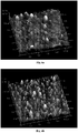
- FIG. 6a showing the AFM image of the top recessed layer surface of the PC-HEMT produced by the manufacturing process of the present invention.
- the measured RMS value of the surface roughness is 0.674 nm in this case.
- Fig. 6b shows the AFM surface image of the top recessed layer of the HEMT made by a conventional manufacturing process.
- the HEMT initially had a top ultrathin-grown AlGaN layer of the 6-7 nm thickness.
- This layer was recessed with inductively-coupled plasma (ICP) for 60 sec using a conventional reactive-ion etching (RIE) technique.
- the measured RMS value of the surface roughness is 1.211 nm in this case.
- FIGs. 6c show the time-dependent plot of the drain-source electric current I DS of the nitrogen oxide sensor measuring 100 ppb of the NO 2 gas in 80%-humid air, where the sensor incorporates the PC-HEMT made by the manufacturing process of the present invention.
- Figs. 6d show the time-dependent plot of the I DS of the nitrogen oxide sensor measuring 100 ppb of the NO 2 gas in 80%-humid air, where the sensor incorporates and based on the HEMT made by the conventional manufacturing process. It is clear from these comparative examples that the manufacturing process of the present invention based on the ultra-low damaging RIE with a narrow plasma-ion energy distribution leads to much lower roughness of the semiconductor surface, which in turn leads to incredibly high sensitivity of the sensor.
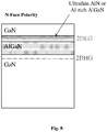
- the hetero-junction structure may be a three-layer structure consisting of two GaN layers and one AlGaN layer squeezed between said buffer layers like in a sandwich, wherein the top layer is a buffer layer.
- This may lead to formation of the two-dimensional hole gas (2DHG) in the top GaN layer above the AlGaN layer which results in reversing polarity of the transistor compared to the two-layer structure discussed above.
- III-V nitride semiconductor materials strongly affects the performance of the transistors based on these semiconductors.
- the quality of the wurtzite GaN materials can be varied by their polarity, because both the incorporation of impurities and the formation of defects are related to the growth mechanism, which in turn depends on surface polarity.
- the occurrence of the 2DEG/2DHG and the optical properties of the hetero-junction structures of nitride-based materials are influenced by the internal field effects caused by spontaneous and piezo-electric polarizations.
- Devices in all of the III-V nitride materials are fabricated on polar ⁇ 0001 ⁇ surfaces.
- any GaN layer has two surfaces with different polarities, a Ga-polar surface and an N-polar surface.
- a Ga-polar surface is defined herein as a surface terminating on a layer of Ga atoms, each of which has one unoccupied bond normal to the surface.
- Each surface Ga atom is bonded to three N atoms in the direction away from the surface.
- an N-polar surface is defined as a surface terminating on a layer of N atoms, each of which has one unoccupied bond normal to the surface.
- Each surface N atom is also bonded to three Ga atoms in the direction away from the surface.
- the N-face polarity structures have the reverse polarity to the Ga-face polarity structures.
- the barrier layer is always placed on top of the buffer layer.
- the layer which is therefore recessed in the two-layer heterojunction structure is the barrier layer, specifically the AlGaN layer.
- the hetero-junction structure is grown along the ⁇ 0001 ⁇ -direction or, in other words, with the Ga-face polarity.
- the physical mechanism that leads to the formation of the 2DEG is a polarisation discontinuity at the AlGaN/GaN interface, reflected by the formation of the polarisation-induced fixed interface charges that attract free carriers to form a two-dimensional carrier gas. It is a positive polarisation charge at the AlGaN/GaN interface that attracts electrons to form 2DEG in the GaN layer slightly below this interface.
- polarity of the interface charges depends on the crystal lattice orientation of the hetero-junction structure, i.e. Ga-face versus N-face polarity, and the position of the respective AlGaN/GaN interface in the hetero-junction structure (above or below the interface). Therefore, different types of the accumulated carriers can be present in the hetero-junction structure of the embodiments.
- the deposition of a dielectric layer on top might be beneficial or even necessary to obtain a better confinement (as in case of the N-face structures).
- the preferable structures of the embodiments are structures "B” and "C".
- the 2DHG conducting channel formed in the top GaN layer which has a higher chemical stability (particularly towards surface oxidation) than the AlGaN layer.
- the 2DEG conducting channel might be closer to the surface. Therefore, the electron mobility might be lower than in the 2DEG structure with the Ga-face polarity.
- the polarity of the heterostructure can be adjusted by the choice of the substrate (e.g. C-face SiC) or by the growth conditions.
- PC-HEMT pseudo-conductive high-electron mobility transistor
- Capacitive coupling is defined as an energy transfer within the same electric circuit or between different electric circuits by means of displacement currents induced by existing electric fields between circuit/s nodes.
- ohmic contacts are the contacts that follow Ohm's law, meaning that the current flowing through them is directly proportional to the voltage.
- Non-ohmic contacts however do not follow the same linear relationship of the Ohm's law. In other words, electric current passing through non-ohmic contacts is not linearly proportional to voltage.
- Fermi level pinning This phenomenon of shifting the centre of the band gap to the Fermi level as a result of a metal-semiconductor contact is defined as "Fermi level pinning", which differs from one semiconductor to another. If the Fermi level is energetically far from the band edge, the Schottky contact would preferably be formed. However, if the Fermi level is close to the band edge, an ohmic contact would preferably be formed.
- the Schottky barrier contact is a rectifying non-ohmic contact, which in reality is almost independent of the semi-conductor or metal work functions.
- a non-ohmic contact allows electric current to flow only in one direction with a non-linear current-voltage curve that looks like that of a diode.
- an ohmic contact allows electric current to flow in both directions roughly equally within normal device operation range, with an almost linear current-voltage relationship that comes close to that of a resistor (hence, "ohmic").
- the DC readout cannot be carried out.
- the AC-frequency regime must be used.
- the AC readout or impedance measurements of the electric current flowing through the 2DEG/2DHG-channel should be performed in this particular case.
- the capacitive coupling of the non-ohmic metal contacts with the 2DEG/2DHG channel becomes possible only if sufficiently high AC frequency, higher than 30 kHz, is applied to the metallizations.
- the electrical metallizations which are capacitively coupled to the 2DEG/2DHG channel utilise the known phenomenon of energy transfer by displacement currents. These displacement currents are induced by existing electrical fields between the electrical metallizations and the 2DEG/2DHG conducting channel operated in the AC frequency mode through the Schottky contact as explained above.
- a tapered slot antenna also known as a Vivaldi antenna is placed in the open gate area of the transistor.
- the Vivaldi-antenna gate is capable of detecting various sub-THz-frequencies, i.e. 200-800 GHz. By applying additional plasmonic filters of any kind, the frequencies could be tuned precisely to a specific frequency of choice.
- a Vivaldi antenna is a co-planar broadband-antenna, which is made from a dielectric plate metalized on both sides.
- Fig. 9 shows the model the model of the Vivaldi antenna realised on a thin dielectric substrate. An exponential function is used for the taper profile. The entire domain is bounded by a perfectly matched layer.
- the tapered slot is patterned with a perfect electric conductor (PEC) ground plane on the top of the Si dielectric substrate. One end of the slot is open to air and the other end is finished with a circular slot.
- PEC perfect electric conductor
- Fig. 10 shows the electric field distribution in the Vivaldi antenna plane at 480 GHz.
- the substrate size is 917x667x4 ⁇ m with total area about 0.6 mm 2 .
- Substrate material is a high-dielectric constant, low conductive semiconductor material with ⁇ > 1000 Obm ⁇ cm, such as for example, Si and GaAs.
- the following table provides the exemplary sub-THz Vivaldi antenna characteristics: Parameter Units Value Comments
- Substrate size ⁇ m 3 917x667x4 Si, GaAs (high dielectric constant material)
- Fig. 11 shows (a) the far-field directional radiation pattern of the Vivaldi antenna starting from 240 GHz till 780 GHz and (b) the corresponding 3D far-field pattern at 480 GHz, with the maximum in the X direction (axis along the substrate), which means this is a unidirectional antenna.
- the feeding line excites a circular space via a microstrip line, terminated with a sector-shaped area. From the circular resonant area the energy reaches an exponential pattern via a symmetrical slot line.
- the frequency response SWR of the Vivaldi antenna shows wide-band impedance matching better than 2:1 in most of the simulated frequency range.
- Printed circuit technology makes this type of antenna cost effective at sub-THz frequencies.
- the Vivaldi antenna is its broadband characteristics suitable for ultra-wideband signals in the sub-THz frequency domain, its easy manufacturing process using common methods for PCB production, and its easy impedance matching to the feeding line using microstrip line modelling methods. Also, the Vivaldi antenna has been chosen because it permits to integrate a long meander delay without having undesired effects.
- the Vivaldi antenna is a reciprocal device. It collects in a passive mode exactly the same frequencies that can be actively radiated. Due to its very broadband character, the Vivaldi antenna may receive signals outside the 240 GHz-780 GHz range. In order to limit the antenna sensitivity to the desired 0.3 THz-0.6 THz range, two-dimensional photonic crystals (18) may be superimposed on top of the antenna metal layer, as shown in Fig. 12 .
- Vivaldi antenna and lattice constant of the photonic crystal are summarised in the following table: Parameter Units Value Comments Antenna substrate ⁇ m 4 Si, GaAs (high dielectric constant material) Device footprint area ⁇ m 2 917x667 Metal layer thickness nm 80 Au Superimposed Si thickness ⁇ m 4 Si or GaAs Distance between the pillars ⁇ m 160 Au or Al Pillar diameter ⁇ m 60 Pillar height ⁇ m 4
- Fig. 13 shows the position of the metal connector (19) on the Vivaldi antenna for coupling with the PC-HEMT of the embodiment.
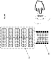
- Fig. 14 schematically shows a microelectronic sensor for biometric authentication, with a remote readout, comprising the following components (this is a single-transistor sub-THz solution):
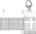
- Fig. 15 schematically shows a microelectronic sensor for biometric authentication, with a remote readout, comprising the following components (this is the DC/RF-based sub-THz antenna transistor-array solution for imaging):
- the ADC card (104) may be any suitable analogue-to-digital converter data logger card that can be purchased, for example, from National Instruments® or LabJack®.
- the current amplifier (103) can be operated directly with current flowing via the 2DEG/2DHG channel into the amplifier with small input resistance of 1M ⁇ at gain higher than 10 4 and only 1 ⁇ at gains lower than 200. This setup may directly amplify the electric current modulation in the 2DEG channel originated from an external body charges.
- the wireless connection module (106) may be a short-range Bluetooth® or NFC providing wireless communication between the wearable device or gadget and a smartphone for up to 20 m. If this module is Wi-Fi, the connection can be established with a network for up to 200 nm, while GSM allows the worldwide communication to a cloud.
- the external memory may be a mobile device (such as a smartphone), desktop computer, server, remote storage, internet storage or telemedicine diagnostics cloud.
- the microelectronic sensor of the present application may be used for portable long-time-operation solution within remote cloud-based biometric authentication.
- the portable microelectronic sensor of the embodiments should have a very small power consumption saving the battery life for a prolong usage.
- the non-ohmic high-resistive contacts capacitively connecting the sensor to an electric circuit are preferable.
- the non-ohmic contacts actually limit an electric current flowing through the 2DEG/2DHG channel by having an electrical resistance 3-4 times higher than the resistance of the 2DEG/2DHG-channel, thereby reducing electrical power consumption without sacrificing sensitivity and functionality of the sensor.
- the use of non-ohmic contacts in some embodiments of the sensor of the present application is a hardware solution allowing to minimise the power consumption of the device.
- the power consumption of the device can be minimised using a software algorithm managing the necessary recording time of the sensor and a battery saver mode, which limits the background data and switches the wireless connection only when it is needed.
- the microelectronic sensor may be integrated within a smartwatch, smartphone or in any other available personal gadget or wearable device, including but not limited to a bracelet, a ring or an earring, with or without any direct skin-contact to the sensor interface. It can be connected to the metallic chassis or to the capacitive sensitive display elements of the smartphone transducing an electrical charge to the sensor.
- the present sensor may replace the fingerprint sensor within the smartphone lock.
- the in-built present sensor is capable of sensing the signals and transmitting them either to a smartphone or directly to a biometric authentication cloud. The biometric authentication can be continuously carried out when the sensor is in a contact with a body, or activated on calling, or when the contact is established.
- biometric authentication cloud The relevant biometric data recorded is then transmitted to a biometric authentication cloud and will be available for further processing. It may also be used in an automotive sector with car locks and bio-vital hemodynamic monitoring of the driver (sleepiness, cardio, stress etc.)
- the microelectronic sensor of the present application may be used in a biometric authentication chip of any security system, in a personal computer, laptop, credit card, any identification card or tag, in an automated teller machine, automatic gate opener, swing gate opener, flap barrier or turnstile gate.
- a method for biometric authentication of a user comprises the following steps:
- Sweat ducts radiation may therefore accurately reflect the biometric pattern of an individual. Sweat ducts are emitting all the time independently of sweating process as they are always filled with a body electrolyte. Since every individual has his/her own sub-THz spectra and his/her own sweat-duct spatial skin-surface pattern, using this unique sub-THz-pattern may allow recording the very unique spectra and spatial duct pattern from each individual and then authenticating them with an unprecedented precision.
- the Vivaldi antenna of the sensor chip of the embodiments is passively receiving these sub-THz signals from sweat ducts in approximately 200-800 GHz range.
- the frequency may be precisely adjusted to a frequency of choice.
- the detection principle is based on the field effect current modulation in a DC-mode within the PC-HEMT 2DEG channel achieved by Vivaldi-shaped gate antenna. Once a user either touches the sensor or approached it at a relatively short distance (in a range of centimetres), the Vivaldi-shaped gate antenna may instantly and strongly concentrate the electric field strength of the sub-THz radiation in a very small area above the ultra charge sensitive 2DEG channel, thereby affecting its conductivity in the DC-mode by accumulation effect.
- the S11-S12 parameters of the sensor may also be measured at RF frequencies of 1-60 GHz using beating effect from the sub-THz-radiation.
- an array containing 10-10,000 sub-THz-pixels may be used.
Landscapes
- Health & Medical Sciences (AREA)
- Life Sciences & Earth Sciences (AREA)
- Engineering & Computer Science (AREA)
- Biomedical Technology (AREA)
- Public Health (AREA)
- Physics & Mathematics (AREA)
- General Health & Medical Sciences (AREA)
- Medical Informatics (AREA)
- Molecular Biology (AREA)
- Veterinary Medicine (AREA)
- Animal Behavior & Ethology (AREA)
- Surgery (AREA)
- Heart & Thoracic Surgery (AREA)
- Pathology (AREA)
- Biophysics (AREA)
- Business, Economics & Management (AREA)
- Microelectronics & Electronic Packaging (AREA)
- General Business, Economics & Management (AREA)
- Computer Hardware Design (AREA)
- General Physics & Mathematics (AREA)
- Electromagnetism (AREA)
- Power Engineering (AREA)
- Condensed Matter Physics & Semiconductors (AREA)
- Nuclear Medicine, Radiotherapy & Molecular Imaging (AREA)
- Primary Health Care (AREA)
- Epidemiology (AREA)
- Radiology & Medical Imaging (AREA)
- Computer Networks & Wireless Communication (AREA)
- Junction Field-Effect Transistors (AREA)
Claims (15)
- Transistor à haute mobilité électronique pseudo-conducteur à grille ouverte pour amplifier des signaux produit par un corps d'un utilisateur dans une plage de rayonnement sub-THz, comprenant :(1) une structure d'hétérojonction multicouche constituée de matériaux semiconducteurs monocristallins ou polycristallins de nitrure de gallium (GaN) et de nitrure d'aluminium-gallium (AlGaN), déposée sur une couche de substrat, dans lequel :(a) ladite structure comprend (i) une couche de GaN de dessus évidée dans une zone de grille ouverte du transistor à l'épaisseur de 5 à 9 nm et ayant la rugosité de surface de 0,2 nm ou moins, (ii) une couche tampon de GaN de dessous, et (iii) une couche barrière d'AlGaN entre elles ; lesdites couches ont une polarité de face Ga, formant ainsi un canal conducteur de gaz de trou bidimensionnel (2DHG) dans la couche de GaN de dessus, près de l'interface avec ladite couche barrière d'AlGaN ; ou(b) ladite structure comprend (i) une couche de GaN de dessus évidée dans une zone de grille ouverte du transistor à l'épaisseur de 5 à 9 nm et ayant la rugosité de surface de 0,2 nm ou moins, (ii) une couche tampon de GaN de dessous, et (iii) une couche barrière d'AlGaN entre elles ; lesdites couches ont une polarité de face N, formant ainsi un canal conducteur de gaz d'électrons bidimensionnel (2DEG) dans la couche de GaN de dessus, près de l'interface avec ladite couche barrière d'AlGaN ; ou(c) ladite structure comprend (i) une couche de d'AlGaN de dessus évidée dans une zone de grille ouverte du transistor à l'épaisseur de 5 à 9 nm et ayant la rugosité de surface de 0,2 nm ou moins, et (ii) une couche tampon de GaN de dessous ; lesdites couches ont une polarité de face N, formant ainsi un canal conducteur de gaz de trou bidimensionnel (2DHG) dans la couche tampon de GaN, près de l'interface avec ladite couche barrière d'AlGaN ;(2) des contacts de source et de drain connectés audit canal conducteur 2DEG ou 2DHG et à des métallisations électriques pour connecter ledit transistor à un circuit électrique ; et(3) une électrode d'antenne Vivaldi placée sur la couche de dessus entre les lesdites zones de contact de source et de drain dans une zone de grille ouverte du transistor et capable de détecter des signaux électriques dans la plage de fréquence sub-THz de 200 à 800 GHz.
- Transistor selon la revendication 1, dans lequel la structure (b) comprend en outre une couche d'AIN ou d'AlGaN supplémentaire ayant une haute teneur en Al et une épaisseur de 1 nm ou moins, dans la couche tampon de GaN de dessus au-dessus du canal 2DEG.
- Transistor selon la revendication 1, dans lequel lesdits contacts de source et de drain sont ohmiques, ou lesdites métallisations électriques sont couplées de manière capacitive audit canal conducteur 2DEG ou 2DHG pour induire des courants de déplacement, aboutissant ainsi au fait que lesdits contacts de source et de drain sont non ohmiques.
- Transistor selon la revendication 1, comprenant en outre une couche diélectrique déposée sur le dessus de ladite structure d'hétérojonction multicouche.
- Transistor selon la revendication 1, dans lequel l'épaisseur de la couche de dessus évidée dans la zone de grille ouverte dudit transistor est de 6 à 7 m, ou de 6,2 nm à 6,4 nm.
- Transistor selon les revendications 1 ou 5, dans lequel la rugosité de surface de la couche de dessus évidée dans la zone de grille ouverte dudit transistor est de 0,1 nm ou moins, ou de 0,05 nm ou moins.
- Transistor selon la revendication 1, dans lequel ladite électrode d'antenne Vivaldi comprend en outre des cristaux photoniques bidimensionnels superposés sur le dessus de sa couche métallique.
- Capteur micro-électronique pour une authentification biométrique d'un utilisateur, avec une lecture à distance, comprenant :(a) au moins un transistor (100) de l'une quelconque des revendications 1 à 7 ;(b) un circuit intégré (101) pour stocker et traiter un signal dans un domaine de fréquence sub-THz, et pour moduler et démoduler des signaux radiofréquence (RF) ;(c) un générateur d'µ-impulsions (102) pour une génération de signaux RF à impulsions ;(d) un amplificateur de courant CC-RF intégré ou amplificateur synchrone (103) connecté audit générateur d'µ-impulsions (102) pour une amplification du signal obtenu depuis ledit générateur d'µ-impulsions ;(e) un convertisseur analogique-numérique (CAN) (104) avec carte d'entrée/de sortie numérique incorporée connecté à l'amplificateur (103) pour convertir le signal analogique reçu en signal numérique et fournir en sortie ledit signal numérique à une unité de microcontrôleur ;(f) l'unité de microcontrôleur (MCU) (105) pour traiter et convertir le signal numérique reçu en données lisibles dans une interface utilisateur ou mémoire externe ; et(g) un module de connexion sans fil (106) pour une connexion sans fil dudit capteur micro-électronique à ladite interface utilisateur ou mémoire externe.
- Capteur micro-électronique pour une authentification biométrique d'un utilisateur, avec une lecture à distance, comprenant :(a) le réseau (110) des transistors (100) de l'une quelconque des revendications 1 à 7, dans lequel chaque transistor dans ledit réseau a une antenne Vivaldi intégrée et est connecté à sa ligne de contact électrique dédiée ;(b) un multiplexeur de rangée (107) connecté audit réseau pour adresser une pluralité desdits transistors agencés en rangées, sélectionner l'un de plusieurs signaux d'entrée analogiques ou numériques et réacheminer l'entrée sélectionnée dans une seule ligne ;(c) un multiplexeur de colonne (108) connecté audit réseau pour adresser une pluralité desdits transistors agencés en colonnes, sélectionner l'un de plusieurs signaux d'entrée analogiques ou numériques et réacheminer l'entrée sélectionnée dans une seule ligne ;(d) un circuit intégré pour stocker et traiter lesdits signaux dans un domaine de fréquence sub-THz, et pour moduler et démoduler des signaux radiofréquence (RF) ;(e) un générateur d'µ-impulsions (102) pour une génération de signaux RF à impulsions ;(f) un amplificateur de courant CC-RF intégré ou amplificateur synchrone (103) connecté audit générateur d'µ-impulsions (102) pour une amplification du signal obtenu depuis ledit générateur d'µ-impulsions ;(g) un convertisseur analogique-numérique (CAN) (104) avec carte d'entrée/de sortie numérique incorporée connecté à l'amplificateur (103) pour convertir le signal analogique reçu en signal numérique et fournir en sortie ledit signal numérique à une unité de microcontrôleur ;(h) l'unité de microcontrôleur (MCU) (105) pour traiter et convertir le signal numérique reçu en données lisibles dans une interface utilisateur ou mémoire externe ; et(i) un module de connexion sans fil (106) pour une connexion sans fil dudit capteur micro-électronique à ladite interface utilisateur ou mémoire externe.
- Capteur micro-électronique selon la revendication 8 ou 9, dans lequel ladite mémoire externe est un dispositif mobile, un ordinateur de bureau, un serveur, un stockage distant, un stockage Internet ou un Cloud d'authentification biométrique.
- Capteur micro-électronique selon l'une quelconque des revendications 8 à 10, dans lequel ledit capteur est intégré au sein d'une montre intelligente, d'un téléphone intelligent ou de tout autre gadget personnel ou dispositif portatif disponible, avec ou sans contact direct de la peau avec l'interface de capteur.
- Capteur micro-électronique selon la revendication 11, dans lequel ledit dispositif portatif est un bracelet, une bague ou une boucle d'oreille.
- Capteur micro-électronique selon l'une quelconque des revendications 8 à 10, dans lequel ledit capteur est connecté à une armature, ou un châssis, ou des éléments d'affichage sensibles capacitifs d'un téléphone intelligent, d'une montre intelligente ou d'un gadget électronique personnel, ledit téléphone intelligent, ladite montre intelligente ou ledit gadget électronique personnel étant capable d'une transduction de charge électrique au capteur.
- Capteur micro-électronique selon l'une quelconque des revendications 8 à 10, dans lequel ledit capteur est un capteur d'empreintes digitales au sein d'un verrou de téléphone intelligent et ou d'un verrou de voiture, ou ledit capteur est intégré dans un module d'authentification biométrique d'un système de sécurité, d'un ordinateur personnel, d'un ordinateur portable, d'un système d'ouverture de portillon automatique, d'un système d'ouverture de portillon pivotant, d'une barrière de trappe, d'un tourniquet, ou d'une machine de caisse automatique, ou ledit capteur est intégré dans une puce d'authentification biométrique d'une carte de crédit ou d'une carte ou étiquette d'identification, ou ledit capteur est approprié pour une utilisation dans la surveillance hémodynamique vitale d'un conducteur dans le but de déterminer la somnolence, la fatigue, la nervosité, le risque cardiaque, le stress et d'autres situations dangereuses pour la conduite d'une voiture.
- Procédé pour une authentification biométrique d'un utilisateur comprenant :(1) la mise en contact d'un point de détection unique sur le corps de l'utilisateur avec le capteur micro-électronique de l'une quelconque des revendications 8 à 14, ou le positionnement à distance dudit capteur dans un espace contre le corps de l'utilisateur, et l'activation dudit capteur à la demande ou lorsque le contact est établi ;(2) l'enregistrement de signaux électriques reçus depuis le corps de l'utilisateur avec ledit capteur micro-électronique sous une forme d'un courant électrique de source-drain du capteur en fonction du temps (dynamique IDS) et/ou la mesure de paramètres S11-S12 du capteur en fonction du temps (dynamique S11-S12) ;(3) la transmission des signaux enregistrés dudit capteur à une mémoire externe pour un traitement supplémentaire ; et(4) la conversion des signaux transmis en signaux numériques, le traitement des signaux numériques dans la mémoire externe, et la comparaison de ladite dynamique IDS et/ou de ladite dynamique S11-S12 à des données biométrique pré-étalonnées de l'utilisateur stockées dans la mémoire externe, pour ainsi authentifier biométriquement l'utilisateur.
Applications Claiming Priority (2)
| Application Number | Priority Date | Filing Date | Title |
|---|---|---|---|
| US201762554098P | 2017-09-05 | 2017-09-05 | |
| PCT/IB2018/056765 WO2019049035A1 (fr) | 2017-09-05 | 2018-09-05 | Capteur microélectronique pour authentification biométrique |
Publications (2)
| Publication Number | Publication Date |
|---|---|
| EP3679649A1 EP3679649A1 (fr) | 2020-07-15 |
| EP3679649B1 true EP3679649B1 (fr) | 2021-06-09 |
Family
ID=64051616
Family Applications (1)
| Application Number | Title | Priority Date | Filing Date |
|---|---|---|---|
| EP18796102.4A Active EP3679649B1 (fr) | 2017-09-05 | 2018-09-05 | Capteur microélectronique pour authentification biométrique |
Country Status (5)
| Country | Link |
|---|---|
| EP (1) | EP3679649B1 (fr) |
| CN (1) | CN111095792A (fr) |
| DK (1) | DK3679649T3 (fr) |
| ES (1) | ES2887734T3 (fr) |
| WO (1) | WO2019049035A1 (fr) |
Families Citing this family (7)
| Publication number | Priority date | Publication date | Assignee | Title |
|---|---|---|---|---|
| WO2020188389A1 (fr) * | 2019-03-21 | 2020-09-24 | Epitronic Holdings Pte. Ltd | Capteur microélectronique comprenant un pc-hemt doté d'une électrode en métamatériau |
| WO2021105839A1 (fr) * | 2019-11-26 | 2021-06-03 | Epitronic Holdings Pte. Ltd. | Capteurs microélectroniques pour réseaux inter-puces pouvant enregistrer et traiter des signaux neuronaux et des potentiels d'action |
| US11749015B2 (en) | 2020-03-13 | 2023-09-05 | Fingerprint Cards Anacatum Ip Ab | Under display terahertz biometric imaging arrangement |
| US11922716B2 (en) | 2020-03-13 | 2024-03-05 | Fingerprint Cards Anacatum Ip Ab | Under display passive terahertz biometric imaging device |
| CN114008690A (zh) * | 2020-03-13 | 2022-02-01 | 指纹卡安娜卡敦知识产权有限公司 | 太赫兹生物特征成像封装 |
| TWI740700B (zh) * | 2020-11-03 | 2021-09-21 | 長庚大學 | 氮化鎵轉阻放大器 |
| US11874223B1 (en) | 2022-08-30 | 2024-01-16 | The Goodyear Tire & Rubber Company | Terahertz characterization of a multi-layered tire tread |
Family Cites Families (4)
| Publication number | Priority date | Publication date | Assignee | Title |
|---|---|---|---|---|
| KR101774933B1 (ko) * | 2010-03-02 | 2017-09-06 | 삼성전자 주식회사 | 듀얼 디플리션을 나타내는 고 전자 이동도 트랜지스터 및 그 제조방법 |
| WO2012151680A1 (fr) | 2011-05-10 | 2012-11-15 | Agrafioti Foteini | Système et procédé permettant une reconnaissance d'identité en continu ou instantanée basée sur des signaux biométriques physiologiques |
| EP2799852A1 (fr) * | 2013-04-29 | 2014-11-05 | Stichting IMEC Nederland | Capteur à base 2DE et dispositif pour détecter un signal ECG |
| US9490518B1 (en) * | 2015-09-28 | 2016-11-08 | Texas Instruments Incorporated | System for launching a signal into a dielectric waveguide |
-
2018
- 2018-09-05 DK DK18796102.4T patent/DK3679649T3/da active
- 2018-09-05 WO PCT/IB2018/056765 patent/WO2019049035A1/fr unknown
- 2018-09-05 ES ES18796102T patent/ES2887734T3/es active Active
- 2018-09-05 CN CN201880057310.3A patent/CN111095792A/zh active Pending
- 2018-09-05 EP EP18796102.4A patent/EP3679649B1/fr active Active
Also Published As
| Publication number | Publication date |
|---|---|
| ES2887734T3 (es) | 2021-12-27 |
| EP3679649A1 (fr) | 2020-07-15 |
| WO2019049035A1 (fr) | 2019-03-14 |
| DK3679649T3 (da) | 2021-09-13 |
| CN111095792A (zh) | 2020-05-01 |
Similar Documents
| Publication | Publication Date | Title |
|---|---|---|
| EP3679649B1 (fr) | Capteur microélectronique pour authentification biométrique | |
| EP3679648B1 (fr) | Capteur microélectronique pour la surveillance non invasive de taux de glucose dans le sang | |
| US10945643B2 (en) | Microelectronic sensor for biometric authentication | |
| US20200221969A1 (en) | Microelectronic sensors for sensing electrical signals from a human body in a sub-terahertz range | |
| US10905346B2 (en) | Pseudo-conductive high-electron mobility transistors and microelectronic sensors based on them | |
| US20200303534A1 (en) | Microelectronic sensor with an aharonov-bohm antenna | |
| WO2017153906A2 (fr) | Transistors pseudo-conducteurs à mobilité électronique élevée et capteurs microélectroniques basés sur ceux-ci | |
| US20220107223A1 (en) | Microelectronic sensor with bolometric or pyroelectric detector for sensing electrical signals in sub-terahertz and terahertz frequency ranges | |
| US10523181B2 (en) | Surface acoustic wave RFID sensor for material and structure sensing | |
| US20200300842A1 (en) | Electronic sorbent assay | |
| US20190021623A1 (en) | Microelectronic sensor for air quality monitoring | |
| Varghese et al. | Fabrication and pH-sensitivity analysis of MOS-HEMT dimensional variants for bio-sensing applications | |
| EP3482495B1 (fr) | Capteur rfid à ondes acoustiques de surface pour accessoires vestimentaires hémodynamiques | |
| EP3942287A1 (fr) | Procédé de détection chimique et biomoléculaire utilisant pc-hemt comprenant une électrode d'antenne vivaldi | |
| CN109475297B (zh) | 用于生物识别认证的微电子传感器 | |
| WO2021181218A1 (fr) | Capteurs micro-électroniques pour surveiller la résistance et la déformation d'un matériau dans des écrous segmentés | |
| WO2021105839A1 (fr) | Capteurs microélectroniques pour réseaux inter-puces pouvant enregistrer et traiter des signaux neuronaux et des potentiels d'action | |
| US11908901B1 (en) | Graphene varactor including ferroelectric material |
Legal Events
| Date | Code | Title | Description |
|---|---|---|---|
| STAA | Information on the status of an ep patent application or granted ep patent |
Free format text: STATUS: UNKNOWN |
|
| STAA | Information on the status of an ep patent application or granted ep patent |
Free format text: STATUS: THE INTERNATIONAL PUBLICATION HAS BEEN MADE |
|
| PUAI | Public reference made under article 153(3) epc to a published international application that has entered the european phase |
Free format text: ORIGINAL CODE: 0009012 |
|
| STAA | Information on the status of an ep patent application or granted ep patent |
Free format text: STATUS: REQUEST FOR EXAMINATION WAS MADE |
|
| 17P | Request for examination filed |
Effective date: 20200331 |
|
| AK | Designated contracting states |
Kind code of ref document: A1 Designated state(s): AL AT BE BG CH CY CZ DE DK EE ES FI FR GB GR HR HU IE IS IT LI LT LU LV MC MK MT NL NO PL PT RO RS SE SI SK SM TR |
|
| AX | Request for extension of the european patent |
Extension state: BA ME |
|
| DAV | Request for validation of the european patent (deleted) | ||
| DAX | Request for extension of the european patent (deleted) | ||
| GRAP | Despatch of communication of intention to grant a patent |
Free format text: ORIGINAL CODE: EPIDOSNIGR1 |
|
| STAA | Information on the status of an ep patent application or granted ep patent |
Free format text: STATUS: GRANT OF PATENT IS INTENDED |
|
| INTG | Intention to grant announced |
Effective date: 20210401 |
|
| GRAS | Grant fee paid |
Free format text: ORIGINAL CODE: EPIDOSNIGR3 |
|
| GRAA | (expected) grant |
Free format text: ORIGINAL CODE: 0009210 |
|
| STAA | Information on the status of an ep patent application or granted ep patent |
Free format text: STATUS: THE PATENT HAS BEEN GRANTED |
|
| AK | Designated contracting states |
Kind code of ref document: B1 Designated state(s): AL AT BE BG CH CY CZ DE DK EE ES FI FR GB GR HR HU IE IS IT LI LT LU LV MC MK MT NL NO PL PT RO RS SE SI SK SM TR |
|
| REG | Reference to a national code |
Ref country code: GB Ref legal event code: FG4D |
|
| REG | Reference to a national code |
Ref country code: AT Ref legal event code: REF Ref document number: 1401317 Country of ref document: AT Kind code of ref document: T Effective date: 20210615 Ref country code: CH Ref legal event code: EP |
|
| REG | Reference to a national code |
Ref country code: DE Ref legal event code: R096 Ref document number: 602018018488 Country of ref document: DE |
|
| REG | Reference to a national code |
Ref country code: IE Ref legal event code: FG4D |
|
| REG | Reference to a national code |
Ref country code: FI Ref legal event code: FGE |
|
| REG | Reference to a national code |
Ref country code: DK Ref legal event code: T3 Effective date: 20210909 |
|
| REG | Reference to a national code |
Ref country code: NL Ref legal event code: FP |
|
| REG | Reference to a national code |
Ref country code: LT Ref legal event code: MG9D |
|
| REG | Reference to a national code |
Ref country code: SE Ref legal event code: TRGR |
|
| PG25 | Lapsed in a contracting state [announced via postgrant information from national office to epo] |
Ref country code: HR Free format text: LAPSE BECAUSE OF FAILURE TO SUBMIT A TRANSLATION OF THE DESCRIPTION OR TO PAY THE FEE WITHIN THE PRESCRIBED TIME-LIMIT Effective date: 20210609 Ref country code: LT Free format text: LAPSE BECAUSE OF FAILURE TO SUBMIT A TRANSLATION OF THE DESCRIPTION OR TO PAY THE FEE WITHIN THE PRESCRIBED TIME-LIMIT Effective date: 20210609 Ref country code: BG Free format text: LAPSE BECAUSE OF FAILURE TO SUBMIT A TRANSLATION OF THE DESCRIPTION OR TO PAY THE FEE WITHIN THE PRESCRIBED TIME-LIMIT Effective date: 20210909 |
|
| PG25 | Lapsed in a contracting state [announced via postgrant information from national office to epo] |
Ref country code: GR Free format text: LAPSE BECAUSE OF FAILURE TO SUBMIT A TRANSLATION OF THE DESCRIPTION OR TO PAY THE FEE WITHIN THE PRESCRIBED TIME-LIMIT Effective date: 20210910 Ref country code: LV Free format text: LAPSE BECAUSE OF FAILURE TO SUBMIT A TRANSLATION OF THE DESCRIPTION OR TO PAY THE FEE WITHIN THE PRESCRIBED TIME-LIMIT Effective date: 20210609 Ref country code: NO Free format text: LAPSE BECAUSE OF FAILURE TO SUBMIT A TRANSLATION OF THE DESCRIPTION OR TO PAY THE FEE WITHIN THE PRESCRIBED TIME-LIMIT Effective date: 20210909 Ref country code: RS Free format text: LAPSE BECAUSE OF FAILURE TO SUBMIT A TRANSLATION OF THE DESCRIPTION OR TO PAY THE FEE WITHIN THE PRESCRIBED TIME-LIMIT Effective date: 20210609 |
|
| REG | Reference to a national code |
Ref country code: ES Ref legal event code: FG2A Ref document number: 2887734 Country of ref document: ES Kind code of ref document: T3 Effective date: 20211227 |
|
| PG25 | Lapsed in a contracting state [announced via postgrant information from national office to epo] |
Ref country code: SK Free format text: LAPSE BECAUSE OF FAILURE TO SUBMIT A TRANSLATION OF THE DESCRIPTION OR TO PAY THE FEE WITHIN THE PRESCRIBED TIME-LIMIT Effective date: 20210609 Ref country code: EE Free format text: LAPSE BECAUSE OF FAILURE TO SUBMIT A TRANSLATION OF THE DESCRIPTION OR TO PAY THE FEE WITHIN THE PRESCRIBED TIME-LIMIT Effective date: 20210609 Ref country code: CZ Free format text: LAPSE BECAUSE OF FAILURE TO SUBMIT A TRANSLATION OF THE DESCRIPTION OR TO PAY THE FEE WITHIN THE PRESCRIBED TIME-LIMIT Effective date: 20210609 Ref country code: SM Free format text: LAPSE BECAUSE OF FAILURE TO SUBMIT A TRANSLATION OF THE DESCRIPTION OR TO PAY THE FEE WITHIN THE PRESCRIBED TIME-LIMIT Effective date: 20210609 Ref country code: RO Free format text: LAPSE BECAUSE OF FAILURE TO SUBMIT A TRANSLATION OF THE DESCRIPTION OR TO PAY THE FEE WITHIN THE PRESCRIBED TIME-LIMIT Effective date: 20210609 Ref country code: PT Free format text: LAPSE BECAUSE OF FAILURE TO SUBMIT A TRANSLATION OF THE DESCRIPTION OR TO PAY THE FEE WITHIN THE PRESCRIBED TIME-LIMIT Effective date: 20211011 |
|
| PG25 | Lapsed in a contracting state [announced via postgrant information from national office to epo] |
Ref country code: PL Free format text: LAPSE BECAUSE OF FAILURE TO SUBMIT A TRANSLATION OF THE DESCRIPTION OR TO PAY THE FEE WITHIN THE PRESCRIBED TIME-LIMIT Effective date: 20210609 |
|
| REG | Reference to a national code |
Ref country code: DE Ref legal event code: R097 Ref document number: 602018018488 Country of ref document: DE |
|
| REG | Reference to a national code |
Ref country code: DE Ref legal event code: R119 Ref document number: 602018018488 Country of ref document: DE |
|
| REG | Reference to a national code |
Ref country code: FI Ref legal event code: MAE |
|
| PLBE | No opposition filed within time limit |
Free format text: ORIGINAL CODE: 0009261 |
|
| STAA | Information on the status of an ep patent application or granted ep patent |
Free format text: STATUS: NO OPPOSITION FILED WITHIN TIME LIMIT |
|
| PG25 | Lapsed in a contracting state [announced via postgrant information from national office to epo] |
Ref country code: FI Free format text: LAPSE BECAUSE OF NON-PAYMENT OF DUE FEES Effective date: 20210905 |
|
| REG | Reference to a national code |
Ref country code: DK Ref legal event code: EBP Effective date: 20210930 |
|
| REG | Reference to a national code |
Ref country code: SE Ref legal event code: EUG |
|
| REG | Reference to a national code |
Ref country code: NL Ref legal event code: MM Effective date: 20211001 |
|
| REG | Reference to a national code |
Ref country code: CH Ref legal event code: PL |
|
| 26N | No opposition filed |
Effective date: 20220310 |
|
| REG | Reference to a national code |
Ref country code: BE Ref legal event code: MM Effective date: 20210930 |
|
| PG25 | Lapsed in a contracting state [announced via postgrant information from national office to epo] |
Ref country code: MC Free format text: LAPSE BECAUSE OF FAILURE TO SUBMIT A TRANSLATION OF THE DESCRIPTION OR TO PAY THE FEE WITHIN THE PRESCRIBED TIME-LIMIT Effective date: 20210609 Ref country code: AL Free format text: LAPSE BECAUSE OF FAILURE TO SUBMIT A TRANSLATION OF THE DESCRIPTION OR TO PAY THE FEE WITHIN THE PRESCRIBED TIME-LIMIT Effective date: 20210609 |
|
| PGFP | Annual fee paid to national office [announced via postgrant information from national office to epo] |
Ref country code: IT Payment date: 20210930 Year of fee payment: 4 |
|
| PG25 | Lapsed in a contracting state [announced via postgrant information from national office to epo] |
Ref country code: NL Free format text: LAPSE BECAUSE OF NON-PAYMENT OF DUE FEES Effective date: 20211001 |
|
| PG25 | Lapsed in a contracting state [announced via postgrant information from national office to epo] |
Ref country code: SE Free format text: LAPSE BECAUSE OF NON-PAYMENT OF DUE FEES Effective date: 20210906 Ref country code: LU Free format text: LAPSE BECAUSE OF NON-PAYMENT OF DUE FEES Effective date: 20210905 Ref country code: IE Free format text: LAPSE BECAUSE OF NON-PAYMENT OF DUE FEES Effective date: 20210905 Ref country code: FR Free format text: LAPSE BECAUSE OF NON-PAYMENT OF DUE FEES Effective date: 20210930 Ref country code: DE Free format text: LAPSE BECAUSE OF NON-PAYMENT OF DUE FEES Effective date: 20220401 Ref country code: BE Free format text: LAPSE BECAUSE OF NON-PAYMENT OF DUE FEES Effective date: 20210930 |
|
| PG25 | Lapsed in a contracting state [announced via postgrant information from national office to epo] |
Ref country code: LI Free format text: LAPSE BECAUSE OF NON-PAYMENT OF DUE FEES Effective date: 20210930 Ref country code: CH Free format text: LAPSE BECAUSE OF NON-PAYMENT OF DUE FEES Effective date: 20210930 |
|
| REG | Reference to a national code |
Ref country code: ES Ref legal event code: FD2A Effective date: 20221026 |
|
| PG25 | Lapsed in a contracting state [announced via postgrant information from national office to epo] |
Ref country code: DK Free format text: LAPSE BECAUSE OF NON-PAYMENT OF DUE FEES Effective date: 20210930 |
|
| REG | Reference to a national code |
Ref country code: DE Ref legal event code: R081 Ref document number: 602018018488 Country of ref document: DE Owner name: RW SOLUTIONS AND INVESTMENTS L.L.C., AE Free format text: FORMER OWNER: EPITRONIC HOLDINGS PTE. LTD., SINGAPORE, SG |
|
| REG | Reference to a national code |
Ref country code: DE Ref legal event code: R082 Ref document number: 602018018488 Country of ref document: DE |
|
| PG25 | Lapsed in a contracting state [announced via postgrant information from national office to epo] |
Ref country code: ES Free format text: LAPSE BECAUSE OF NON-PAYMENT OF DUE FEES Effective date: 20210906 |
|
| REG | Reference to a national code |
Ref country code: AT Ref legal event code: UEP Ref document number: 1401317 Country of ref document: AT Kind code of ref document: T Effective date: 20210609 |
|
| GBPC | Gb: european patent ceased through non-payment of renewal fee |
Effective date: 20220905 |
|
| PG25 | Lapsed in a contracting state [announced via postgrant information from national office to epo] |
Ref country code: CY Free format text: LAPSE BECAUSE OF FAILURE TO SUBMIT A TRANSLATION OF THE DESCRIPTION OR TO PAY THE FEE WITHIN THE PRESCRIBED TIME-LIMIT Effective date: 20210609 |
|
| PG25 | Lapsed in a contracting state [announced via postgrant information from national office to epo] |
Ref country code: HU Free format text: LAPSE BECAUSE OF FAILURE TO SUBMIT A TRANSLATION OF THE DESCRIPTION OR TO PAY THE FEE WITHIN THE PRESCRIBED TIME-LIMIT; INVALID AB INITIO Effective date: 20180905 |
|
| PG25 | Lapsed in a contracting state [announced via postgrant information from national office to epo] |
Ref country code: IT Free format text: LAPSE BECAUSE OF NON-PAYMENT OF DUE FEES Effective date: 20220905 Ref country code: GB Free format text: LAPSE BECAUSE OF NON-PAYMENT OF DUE FEES Effective date: 20220905 |
|
| PG25 | Lapsed in a contracting state [announced via postgrant information from national office to epo] |
Ref country code: MK Free format text: LAPSE BECAUSE OF FAILURE TO SUBMIT A TRANSLATION OF THE DESCRIPTION OR TO PAY THE FEE WITHIN THE PRESCRIBED TIME-LIMIT Effective date: 20210609 |