EP3679598B1 - Systems and methods for combining optical metrology with mass metrology - Google Patents
Systems and methods for combining optical metrology with mass metrology Download PDFInfo
- Publication number
- EP3679598B1 EP3679598B1 EP18854360.7A EP18854360A EP3679598B1 EP 3679598 B1 EP3679598 B1 EP 3679598B1 EP 18854360 A EP18854360 A EP 18854360A EP 3679598 B1 EP3679598 B1 EP 3679598B1
- Authority
- EP
- European Patent Office
- Prior art keywords
- substrate
- mass
- spectra
- metrology
- model
- Prior art date
- Legal status (The legal status is an assumption and is not a legal conclusion. Google has not performed a legal analysis and makes no representation as to the accuracy of the status listed.)
- Active
Links
- 230000003287 optical effect Effects 0.000 title claims description 81
- 238000000034 method Methods 0.000 title claims description 74
- 239000000758 substrate Substances 0.000 claims description 204
- 238000005259 measurement Methods 0.000 claims description 78
- 238000001228 spectrum Methods 0.000 claims description 59
- 238000009826 distribution Methods 0.000 claims description 33
- 238000012545 processing Methods 0.000 claims description 28
- 238000000513 principal component analysis Methods 0.000 claims description 15
- 239000000835 fiber Substances 0.000 claims description 14
- 238000011282 treatment Methods 0.000 claims description 13
- 238000010801 machine learning Methods 0.000 claims description 12
- 238000000611 regression analysis Methods 0.000 claims description 9
- 239000000463 material Substances 0.000 claims description 8
- 238000004458 analytical method Methods 0.000 claims description 6
- 238000003066 decision tree Methods 0.000 claims description 5
- 238000007637 random forest analysis Methods 0.000 claims description 5
- 238000012706 support-vector machine Methods 0.000 claims description 5
- 238000004519 manufacturing process Methods 0.000 description 27
- 238000012549 training Methods 0.000 description 20
- 238000013528 artificial neural network Methods 0.000 description 16
- 235000012431 wafers Nutrition 0.000 description 16
- 239000004065 semiconductor Substances 0.000 description 13
- 238000000151 deposition Methods 0.000 description 6
- 210000002569 neuron Anatomy 0.000 description 6
- 230000008021 deposition Effects 0.000 description 5
- 238000010586 diagram Methods 0.000 description 5
- 238000013459 approach Methods 0.000 description 4
- 238000000231 atomic layer deposition Methods 0.000 description 4
- 238000005229 chemical vapour deposition Methods 0.000 description 4
- 238000005530 etching Methods 0.000 description 4
- 238000005240 physical vapour deposition Methods 0.000 description 4
- XUIMIQQOPSSXEZ-UHFFFAOYSA-N Silicon Chemical compound [Si] XUIMIQQOPSSXEZ-UHFFFAOYSA-N 0.000 description 3
- 238000004140 cleaning Methods 0.000 description 3
- 230000005484 gravity Effects 0.000 description 3
- 239000011159 matrix material Substances 0.000 description 3
- 229910052710 silicon Inorganic materials 0.000 description 3
- 239000010703 silicon Substances 0.000 description 3
- 230000003595 spectral effect Effects 0.000 description 3
- 230000003068 static effect Effects 0.000 description 3
- 238000012546 transfer Methods 0.000 description 3
- 239000013598 vector Substances 0.000 description 3
- VYPSYNLAJGMNEJ-UHFFFAOYSA-N Silicium dioxide Chemical compound O=[Si]=O VYPSYNLAJGMNEJ-UHFFFAOYSA-N 0.000 description 2
- 210000004027 cell Anatomy 0.000 description 2
- 230000002596 correlated effect Effects 0.000 description 2
- 238000011066 ex-situ storage Methods 0.000 description 2
- 239000007789 gas Substances 0.000 description 2
- 238000003384 imaging method Methods 0.000 description 2
- 238000011065 in-situ storage Methods 0.000 description 2
- 239000002184 metal Substances 0.000 description 2
- 229910052751 metal Inorganic materials 0.000 description 2
- 238000012935 Averaging Methods 0.000 description 1
- 239000000654 additive Substances 0.000 description 1
- 230000000996 additive effect Effects 0.000 description 1
- 238000004891 communication Methods 0.000 description 1
- 230000001276 controlling effect Effects 0.000 description 1
- 238000001816 cooling Methods 0.000 description 1
- 230000000875 corresponding effect Effects 0.000 description 1
- 238000013480 data collection Methods 0.000 description 1
- 230000007423 decrease Effects 0.000 description 1
- 238000013135 deep learning Methods 0.000 description 1
- 238000001312 dry etching Methods 0.000 description 1
- 239000012530 fluid Substances 0.000 description 1
- 230000006870 function Effects 0.000 description 1
- 238000010438 heat treatment Methods 0.000 description 1
- 239000012212 insulator Substances 0.000 description 1
- 238000005468 ion implantation Methods 0.000 description 1
- 239000010410 layer Substances 0.000 description 1
- 238000012417 linear regression Methods 0.000 description 1
- 238000003754 machining Methods 0.000 description 1
- 150000002739 metals Chemical class 0.000 description 1
- NJPPVKZQTLUDBO-UHFFFAOYSA-N novaluron Chemical compound C1=C(Cl)C(OC(F)(F)C(OC(F)(F)F)F)=CC=C1NC(=O)NC(=O)C1=C(F)C=CC=C1F NJPPVKZQTLUDBO-UHFFFAOYSA-N 0.000 description 1
- -1 oxides Substances 0.000 description 1
- 238000000053 physical method Methods 0.000 description 1
- 238000007747 plating Methods 0.000 description 1
- 238000005498 polishing Methods 0.000 description 1
- 238000004886 process control Methods 0.000 description 1
- 238000011160 research Methods 0.000 description 1
- 235000012239 silicon dioxide Nutrition 0.000 description 1
- 239000000377 silicon dioxide Substances 0.000 description 1
- 238000010183 spectrum analysis Methods 0.000 description 1
- 239000000126 substance Substances 0.000 description 1
- 238000001039 wet etching Methods 0.000 description 1
Images


Classifications
-
- H—ELECTRICITY
- H01—ELECTRIC ELEMENTS
- H01L—SEMICONDUCTOR DEVICES NOT COVERED BY CLASS H10
- H01L22/00—Testing or measuring during manufacture or treatment; Reliability measurements, i.e. testing of parts without further processing to modify the parts as such; Structural arrangements therefor
- H01L22/30—Structural arrangements specially adapted for testing or measuring during manufacture or treatment, or specially adapted for reliability measurements
-
- G—PHYSICS
- G01—MEASURING; TESTING
- G01N—INVESTIGATING OR ANALYSING MATERIALS BY DETERMINING THEIR CHEMICAL OR PHYSICAL PROPERTIES
- G01N21/00—Investigating or analysing materials by the use of optical means, i.e. using sub-millimetre waves, infrared, visible or ultraviolet light
- G01N21/17—Systems in which incident light is modified in accordance with the properties of the material investigated
- G01N21/25—Colour; Spectral properties, i.e. comparison of effect of material on the light at two or more different wavelengths or wavelength bands
-
- G—PHYSICS
- G01—MEASURING; TESTING
- G01B—MEASURING LENGTH, THICKNESS OR SIMILAR LINEAR DIMENSIONS; MEASURING ANGLES; MEASURING AREAS; MEASURING IRREGULARITIES OF SURFACES OR CONTOURS
- G01B11/00—Measuring arrangements characterised by the use of optical techniques
- G01B11/02—Measuring arrangements characterised by the use of optical techniques for measuring length, width or thickness
- G01B11/06—Measuring arrangements characterised by the use of optical techniques for measuring length, width or thickness for measuring thickness ; e.g. of sheet material
- G01B11/0616—Measuring arrangements characterised by the use of optical techniques for measuring length, width or thickness for measuring thickness ; e.g. of sheet material of coating
- G01B11/0625—Measuring arrangements characterised by the use of optical techniques for measuring length, width or thickness for measuring thickness ; e.g. of sheet material of coating with measurement of absorption or reflection
-
- G—PHYSICS
- G01—MEASURING; TESTING
- G01B—MEASURING LENGTH, THICKNESS OR SIMILAR LINEAR DIMENSIONS; MEASURING ANGLES; MEASURING AREAS; MEASURING IRREGULARITIES OF SURFACES OR CONTOURS
- G01B11/00—Measuring arrangements characterised by the use of optical techniques
- G01B11/02—Measuring arrangements characterised by the use of optical techniques for measuring length, width or thickness
- G01B11/06—Measuring arrangements characterised by the use of optical techniques for measuring length, width or thickness for measuring thickness ; e.g. of sheet material
-
- G—PHYSICS
- G06—COMPUTING; CALCULATING OR COUNTING
- G06F—ELECTRIC DIGITAL DATA PROCESSING
- G06F30/00—Computer-aided design [CAD]
- G06F30/20—Design optimisation, verification or simulation
-
- G—PHYSICS
- G06—COMPUTING; CALCULATING OR COUNTING
- G06N—COMPUTING ARRANGEMENTS BASED ON SPECIFIC COMPUTATIONAL MODELS
- G06N20/00—Machine learning
-
- H—ELECTRICITY
- H01—ELECTRIC ELEMENTS
- H01L—SEMICONDUCTOR DEVICES NOT COVERED BY CLASS H10
- H01L22/00—Testing or measuring during manufacture or treatment; Reliability measurements, i.e. testing of parts without further processing to modify the parts as such; Structural arrangements therefor
- H01L22/10—Measuring as part of the manufacturing process
- H01L22/12—Measuring as part of the manufacturing process for structural parameters, e.g. thickness, line width, refractive index, temperature, warp, bond strength, defects, optical inspection, electrical measurement of structural dimensions, metallurgic measurement of diffusions
-
- G—PHYSICS
- G01—MEASURING; TESTING
- G01B—MEASURING LENGTH, THICKNESS OR SIMILAR LINEAR DIMENSIONS; MEASURING ANGLES; MEASURING AREAS; MEASURING IRREGULARITIES OF SURFACES OR CONTOURS
- G01B2210/00—Aspects not specifically covered by any group under G01B, e.g. of wheel alignment, caliper-like sensors
- G01B2210/56—Measuring geometric parameters of semiconductor structures, e.g. profile, critical dimensions or trench depth
-
- G—PHYSICS
- G01—MEASURING; TESTING
- G01N—INVESTIGATING OR ANALYSING MATERIALS BY DETERMINING THEIR CHEMICAL OR PHYSICAL PROPERTIES
- G01N2201/00—Features of devices classified in G01N21/00
- G01N2201/08—Optical fibres; light guides
-
- G—PHYSICS
- G06—COMPUTING; CALCULATING OR COUNTING
- G06N—COMPUTING ARRANGEMENTS BASED ON SPECIFIC COMPUTATIONAL MODELS
- G06N20/00—Machine learning
- G06N20/10—Machine learning using kernel methods, e.g. support vector machines [SVM]
-
- G—PHYSICS
- G06—COMPUTING; CALCULATING OR COUNTING
- G06N—COMPUTING ARRANGEMENTS BASED ON SPECIFIC COMPUTATIONAL MODELS
- G06N20/00—Machine learning
- G06N20/20—Ensemble learning
-
- G—PHYSICS
- G06—COMPUTING; CALCULATING OR COUNTING
- G06N—COMPUTING ARRANGEMENTS BASED ON SPECIFIC COMPUTATIONAL MODELS
- G06N7/00—Computing arrangements based on specific mathematical models
- G06N7/01—Probabilistic graphical models, e.g. probabilistic networks
Definitions
- the substrate includes a plurality of dies.
- the optical sensors have a beam diameter that generates samples from portions of a plurality of contiguous dies.
- the learned model is generated by correlating the spectra from a plurality of measurement locations of a plurality of sample substrates with at least one of thickness data, critical dimension data, depth data and material density data generated by a standalone metrology station for the plurality of measurement locations for the plurality of sample substrates.
- the optical sensors 136 may use a large beam diameter.
- the substrate 114 may include a plurality of dies 180 arranged adjacent to one another.
- the optical sensors 136 may have a beam diameter that at least partially captures data from a plurality of dies (for example, at least nine adjacent dies 180). Using a larger beam removes the dependence of the measurements on the precise landing spot and allows efficient spatial averaging across several dies.
- the optical metrology system During the production mode, the optical metrology system generates the spectra as described above. The spectra are fed to the learned model, which generates physical parameters such as thickness data or other substrate physical parameters for the plurality of measurement locations of the substrate.
- the mass metrology station generates mass or mass change data for each of the substrates. The mass change data can be generated using pre- and post-measurements of the substrates.
- the learned model generated during the training mode is used during production to convert the principal component analysis to thickness values or other parameters.
- the thicknesses at the measurement locations are used by the spatial thickness distribution module to determine parameters of the spatial thickness distribution model of the top surface of the substrate.
- the mass or mass change measurement is used as a constraint or boundary condition during regression analysis.
- the thickness, spatial thickness distribution model or other parameters are used to adjust process parameters.
- the phrase at least one of A, B, and C should be construed to mean a logical (A OR B OR C), using a non-exclusive logical OR, and should not be construed to mean "at least one of A, at least one of B, and at least one of C.”
- the controller may be programmed to control any of the processes disclosed herein, including the delivery of processing gases, temperature settings (e.g., heating and/or cooling), pressure settings, vacuum settings, power settings, radio frequency (RF) generator settings, RF matching circuit settings, frequency settings, flow rate settings, fluid delivery settings, positional and operation settings, wafer transfers into and out of a tool and other transfer tools and/or load locks connected to or interfaced with a specific system.
- temperature settings e.g., heating and/or cooling
- RF radio frequency
- the controller may be defined as electronics having various integrated circuits, logic, memory, and/or software that receive instructions, issue instructions, control operation, enable cleaning operations, enable endpoint measurements, and the like.
- the integrated circuits may include chips in the form of firmware that store program instructions, digital signal processors (DSPs), chips defined as application specific integrated circuits (ASICs), and/or one or more microprocessors, or microcontrollers that execute program instructions (e.g., software).
- Program instructions may be instructions communicated to the controller in the form of various individual settings (or program files), defining operational parameters for carrying out a particular process on or for a semiconductor wafer or to a system.
- the controller may be a part of or coupled to a computer that is integrated with the system, coupled to the system, otherwise networked to the system, or a combination thereof.
- the controller may be in the "cloud" or all or a part of a fab host computer system, which can allow for remote access of the wafer processing.
- the computer may enable remote access to the system to monitor current progress of fabrication operations, examine a history of past fabrication operations, examine trends or performance metrics from a plurality of fabrication operations, to change parameters of current processing, to set processing steps to follow a current processing, or to start a new process.
- a remote computer e.g. a server
- the remote computer may include a user interface that enables entry or programming of parameters and/or settings, which are then communicated to the system from the remote computer.
- the controller receives instructions in the form of data, which specify parameters for each of the processing steps to be performed during one or more operations. It should be understood that the parameters may be specific to the type of process to be performed and the type of tool that the controller is configured to interface with or control.
- the controller may be distributed, such as by comprising one or more discrete controllers that are networked together and working towards a common purpose, such as the processes and controls described herein.
- An example of a distributed controller for such purposes would be one or more integrated circuits on a chamber in communication with one or more integrated circuits located remotely (such as at the platform level or as part of a remote computer) that combine to control a process on the chamber.
- example systems may include a plasma etch chamber or module, a deposition chamber or module, a spin-rinse chamber or module, a metal plating chamber or module, a clean chamber or module, a bevel edge etch chamber or module, a physical vapor deposition (PVD) chamber or module, a chemical vapor deposition (CVD) chamber or module, an atomic layer deposition (ALD) chamber or module, an atomic layer etch (ALE) chamber or module, an ion implantation chamber or module, a track chamber or module, and any other semiconductor processing systems that may be associated or used in the fabrication and/or manufacturing of semiconductor wafers.
- PVD physical vapor deposition
- CVD chemical vapor deposition
- ALD atomic layer deposition
- ALE atomic layer etch
- the controller might communicate with one or more of other tool circuits or modules, other tool components, cluster tools, other tool interfaces, adjacent tools, neighboring tools, tools located throughout a factory, a main computer, another controller, or tools used in material transport that bring containers of wafers to and from tool locations and/or load ports in a semiconductor manufacturing factory.
Description
- This application claims priority to
U.S. Utility Application No. 15/696,768, filed on September 6, 2017 - The present disclosure relates to substrate processing systems, and more particularly to systems and methods for combining optical and mass metrology.
- The background description provided here is for the purpose of generally presenting the context of the disclosure.
- Electronic devices are fabricated on substrates such as semiconductor wafers using a variety of processing techniques such as deposition, etching, cleaning and/or other treatments. Examples of deposition techniques include chemical vapor deposition (CVD), physical vapor deposition (PVD), atomic layer deposition (ALD), etc. Examples of removal or etching techniques include stripping, wet etching, dry etching, chemical mechanical polishing (CMP), etc.
- These substrate treatments typically cause changes to a surface of the substrate and/or to the mass of the substrate. For example, deposition generally increases the mass of the substrate while etching generally decreases the mass of the substrate. During production, it is desirable to assess the substrates to determine whether processing is being performed correctly and/or to adjust the process prior to production of subsequent substrates.
- Mass metrology systems have been developed to measure the mass or the change in mass of a substrate during processing. While mass metrology systems are fairly accurate, use of the mass data that is generated is somewhat limited. For example, a mass change during a process may occur due to multiple factors. Some causes of changes in mass are correlated changes. Some changes in mass are distributed across the substrate and may generate zero mass change. While some processes combine mass metrology systems with other metrology systems, the cost tends to be too high.
US 2007/249071 A1 describes methods and apparatuses that may be utilized to perform spectral analysis to monitor a process for fabricating integrated circuit devices on semiconductor substrates (e.g., silicon substrates, silicon on insulator (SOI) substrates, and the like), flat panel displays, solar panels, or other electronic devices. For example, in one embodiment, a method may provide process control by utilizing substrate state information derived from a reflectance signal collected at a designated area of a substrate under process and other related data, in combination, as training data, to train a neural network. The method uses related measurement data of structures at pre-etch, during etch, and post-etch (i.e., substrate state information) stages of a processing step to train a neural network (for example, a multilayer perceptron network) in order to adjust process time and control the operational status of a substrate processing equipment. For example, the method may be used to make improved real time etch depth predictions during an etch process. Data collection may be performed in-situ using a dynamic optical measuring tool capable of taking measurements at desig-nated locations on a substrate, or it may be performed ex-situ; alternatively, it may be performed both in-situ and ex-situ for training the neural network to generate a working model. In this way, the system may dynamically estimate the etch depth ( e.g., etch depth of a feature on a substrate) with high accuracy and high computational speed based on a series of measured optical signal intensities, film thicknesses and/or any other physical parameters by utilizing a neural network.
US 2012/226644 A1 describes approaches for accurate and fast neural network training for library-based CD metrology. In an embodiment, a method of accurate neural network training for library-based CD metrology includes optimizing a threshold for a principal component analysis (PCA) of a spectrum data set to provide a principal component (PC) value. The method also includes estimating a training target for one or more neural networks. The method also includes training the one or more neural networks based on the PC value and the training target. The method also includes providing a spectral library based on the one or more trained neural networks. In one embodiment, optimizing the threshold for the PCA includes determining a lowest level spectrum domain. In an embodiment, a method of fast neural network training for library-based CD metrology includes providing a training target for a first neural network. The method also includes training the first neural network, the training including starting with a predetermined number of neurons and iteratively increasing the number of neurons until an optimized total number of neurons is reached. The method also includes generating a second neural network based on the training and the optimized total number of neu-rons. The method also includes providing a spectral library based on the second neural network. In one embodiment, iteratively increasing the number of neurons until the opti-mized total number of neurons is reached includes using a modified Levenberg-Marquardt approach.US 2005/020073 A1 describes a method for determining endpoint of plasma processing of a semiconductor wafer includes providing a light source, and providing a lens system to collimate and align light from the light source to an active surface of the semiconductor wafer. A plurality of light detector fibers are interleaved among light source fibers which transmit light from the light source to the lens system. Reflected light from the active surface of the semiconductor wafer is received by a plurality of light detector fibers and provided to an imaging spec-trometer. The received reflected light is analyzed by the imaging spectrometer, and matched to a model optical signal. The matched optical signal is selected to determine endpoint or other state of the plasma processing. - A metrology system for substrate processing includes an optical metrology station including a plurality of optical sensors to measure spectra from a plurality of measurement locations on a substrate. A plurality of fiber cables are connected to the plurality of optical sensors. A spectrometer is selectively connected to the plurality of fiber cables. A mass metrology station measures at least one of a mass or mass change of the substrate. A controller includes a modelling module to generate thickness values at the plurality of measurement locations based on the spectra from the plurality of measurement locations and a learned model. A spatial modelling module generates a spatial thickness distribution model for the substrate based on the thickness values at the plurality of measurement locations from the modelling module and the at least one of the mass or the mass change from the mass metrology station. The learned model used to convert the spectral data into the thickness values is generated using machining learning. The mass or mass change is used by the spatial modelling module as a constraint or boundary condition for regression analysis to determine thickness of the substrate at locations other than the measurement locations. The metrology system according to the invention is specified in claim 1.
- In other features, a plurality of shutters is connected to the plurality of fiber cables, respectively. The plurality of shutters is configured to sequentially output spectra from one of the plurality of fiber cables at a time to the spectrometer. The machine learning includes a supervised learning model selected from a group consisting of linear models, support vector machine models, decision tree models, random forest models and Gaussian models. The learned model is based on a first-principle model. The first-principle model is selected from a group consisting of Fresnel multi-beam interference, rigorous coupled-wave analysis (RCWA), or finite-difference time-domain (FDTD).
- In other features, the substrate includes a plurality of dies. The optical sensors have a beam diameter that generates samples from portions of a plurality of contiguous dies. The learned model is generated by correlating the spectra from a plurality of measurement locations of a plurality of sample substrates with at least one of thickness data, critical dimension data, depth data and material density data generated by a standalone metrology station for the plurality of measurement locations for the plurality of sample substrates.
- In other features, the learned model is generated by performing principal component analysis.
- In other features, the learned model is generated using an autoencoder. An optical sensor positioner adjusts a position of at least one of the optical sensors. A substrate support positioner adjusts a position of the substrate support. The plurality of optical sensors measure spectra from opposing surfaces of the substrate.
- In other features, the spatial modelling module generates the spatial thickness distribution model for the substrate further based a thickness of the substrate prior to film treatment.
- A method for providing metrology for substrate processing includes providing an optical metrology station including a plurality of optical sensors to measure spectra from a plurality of measurement locations on a substrate; measuring at least one of a mass or mass change of the substrate; generating thickness values at the plurality of measurement locations of the substrate based on the spectra from the plurality of measurement locations and a learned model; and generating a spatial thickness distribution model for the substrate based on the thickness values at the plurality of measurement locations and the at least one of the mass or the mass change. The method according to the invention is specified in claim 10.
- In embodiments, the machine learning includes a supervised learning model selected from a group consisting of linear models, support vector machine models, decision tree models, random forest models and Gaussian models. The model is based on a first-principle model. The first-principle model is selected from a group consisting of Fresnel multi-beam interference, rigorous coupled-wave analysis (RCWA), or finite-difference time-domain (FDTD).
- In other features, the substrate includes a plurality of dies. The optical sensors have a beam diameter sufficient to generate samples from portions of a plurality of contiguous dies.
- In other features, the method includes generating the learned model by correlating the spectra from a plurality of measurement locations of a plurality of sample substrates with at least one of thickness data, critical dimension data, depth data and material density data generated by a standalone metrology station for the plurality of measurement locations for the plurality of sample substrates.
- In other features, the method includes generating the model by performing principal component analysis.
- In other features, the method includes generating the learned model using autoencoding. The method includes adjusting a position of at least one of the optical sensors during measurement of the spectra for the substrate. The method includes adjusting a position of the substrate support during measurement of the spectra for the substrate. The method includes measuring spectra from opposing surfaces of the substrate.
- In other features, the method includes generating a thickness of the substrate prior to film treatment and generating the spatial thickness distribution model for the substrate further based the thickness of the substrate prior to film treatment.
- Further areas of applicability of the present disclosure will become apparent from the detailed description, the claims and the drawings. The detailed description and specific examples are intended for purposes of illustration only and are not intended to limit the scope of the disclosure.
- The present disclosure will become more fully understood from the detailed description and the accompanying drawings, wherein:
-
FIG. 1A is a functional block diagram of an example of a metrology system according to the present disclosure configured for model training; -
FIG. 1B is a functional block diagram of an example of positioning devices for the optical sensors and/or the substrate support according to the present disclosure; -
FIG. 1C is a functional block diagram of another example of positioning devices for the optical sensors and/or the substrate support according to the present disclosure; -
FIG. 1D is a functional block diagram of an example of optical sensors arranged above and below the substrate according to the present disclosure; -
FIG. 2A illustrates a substrate including a notch according to the present disclosure; -
FIG. 2B is a plan view of an example of large optical sensor beam relative to a plurality of dies of a substrate according to the present disclosure; -
FIG. 3 illustrates an example of a spatial thickness distribution model for a substrate according to the present disclosure; -
FIGs. 4A and 4B are flowcharts illustrating examples of a method for generating a model relating measured spectra to substrate thickness using target reference values generated by a standalone metrology system according to the present disclosure; -
FIG. 5 is a functional block diagram of an example of a metrology system according to the present disclosure configured for production according to the present disclosure; and -
FIGs. 6 and7 are flowcharts illustrating examples of methods for using the learned model, the spectra generated by the optical metrology station and the mass generated by the mass metrology station to determine substrate parameters and/or to adjust process parameters according to the present disclosure. - In the drawings, reference numbers may be reused to identify similar and/or identical elements.
- Systems and methods according to the present disclosure relate to a metrology system that combines both optical metrology and mass metrology into a cost effective and accurate metrology system. As can be appreciated, the process that is to be monitored can be an additive process such as deposition, a subtractive process such as stripping or etching, or other treatment process such as cleaning.
- During a training mode of a learned model and a subsequent production mode, the metrology system uses an optical metrology station including a plurality of optical sensors and a spectrometer. The spectrometer generates spectra at a plurality of measurement locations for each of a plurality of substrates. The spectra are stored along with substrate identification and location identifying data. The spectra are measured at multiple different wavelengths.
- A high-cost, high-accuracy standalone metrology station having spatial resolution is also used to generate reference measurements for the plurality of substrates. The reference measurements are related to substrate parameters at the plurality of measurement locations for at least the same set of substrates. The substrate parameters measured by the standalone metrology station include at least one of thickness data, critical dimension data, depth data and/or material density data. Target reference values are based on the measurements generated by the standalone metrology station. The target reference values are stored with substrate identification and location identifying data.
- Modeling is used to correlate the spectra and the target reference values and to generate a learned model. Subsequently, the learned model is used to convert the spectra for production substrates into physical substrate parameters (such as thickness at particular locations of the substrates) as will be described further below.
- When ramping up to production volumes, the substrate processing systems and metrology systems are duplicated to scale production of the substrates. The relatively high cost of the standalone metrology system typically makes it too costly to use during production. According to the present disclosure, the standalone metrology system is replaced by a less-expensive mass metrology station and the expensive standalone metrology system is no longer needed, which reduces cost.
- During production, the optical metrology system generates the spectra for the production substrates as described above. The spectra are fed to the learned model, which generates physical parameters such as thickness data or other substrate physical parameters for the plurality of measurement locations of the substrate. A mass metrology station is used to generate mass or mass change data for each of the substrates.
- The thickness data for the measured locations is provided as inputs to a spatial thickness distribution module, which determines a surface model or curvature of the top surface of the substrate. The spatial model defines the thickness of the substrate or a layer thereof across the entire surface of the substrate. The mass or mass change is used by the spatial thickness distribution module (the spatial modelling module) as a constraint or boundary condition for regression analysis. In other words, the density of the layer added or removed is known and the mass change is also known. Therefore the mass or mass change is used to constrain the spatial model. The resulting spatial thickness distribution model of the substrate surface is used to determine the thickness of the top surface of the substrate at locations other than the measurement locations. The thickness can be used in conjunction with the mass or mass change to diagnose system performance and to make changes to process parameters for production of subsequent substrates.
- Referring now to
FIG. 1A , ametrology system 100 is shown during training. A substrate transport andhandling system 128 may include one or more robots, transfer stations, and/or other devices for transporting and delivering the substrates to the metrology stations of themetrology system 100. In some examples, the substrates are accurately positioned by a system including a robot and a camera, although other methods can be used. For example, suitable systems for positioning the substrate are described in commonly-assignedU.S. Patent Publication No. 20170028560, which is published on February 2, 2017 and is entitled "System and Method for Wafer Alignment and Centering with CCD Camera and Robot". - The
metrology system 100 includes astandalone metrology station 110 to generate target reference values that are used to generate the learned model. In some examples, thestandalone metrology station 110 includes asubstrate support 112. Asubstrate 114 is arranged on thesubstrate support 112 and physical measurements are made on thesubstrate 114. In some examples, thestandalone metrology station 110 is a high-cost, high-accuracy metrology station such as an optical metrology station. Thestandalone metrology station 110 generates high accuracy metrology data. Target reference values, as will be described further below, are generated by thestandalone metrology station 110 for at least the measurement locations used by the optical metrology station described below. In some examples, the target measurements made by thestandalone metrology station 110 include at least one of thickness data, critical dimension data, depth data and at least material density data. - The
metrology system 100 further includes anoptical metrology station 126. Theoptical metrology station 126 includes asubstrate support 130 supporting thesubstrate 114 during optical metrology measurements. Theoptical metrology station 126 generates optical spectra at the plurality of measurement locations on the substrate. - The
optical metrology station 126 includes a plurality of optical sensors 136-1, 136-2, ..., and 136-X (collectively optical sensors 136) for each of the plurality of measurement locations, where X is an integer greater than one. Each of the plurality of optical sensors 136-1, 136-2, ..., and 136-X is connected by a fiber cable 138-1, 138-2, ..., and 138-X (collectively fiber cables 138) to aspectrometer 150. Amultiplexer 140 including a plurality of shutters 142-1, 142-2, ..., and 142-X (collectively shutters 142) may be used to output a selected one of thefiber cables 138 to thespectrometer 150. - As will be described further below, the
standalone metrology station 110 and/or theoptical metrology station 126 may include one ormore sensors 152 such as optical sensors, cameras, physical sensors, etc. to sense a position of the substrate relative to the substrate support and a control system for adjusting the position of the substrate as needed. For example, an x-y axis position of the substrate is determined in a plane parallel to an upper surface of thesubstrate support 112 and/or 130 and/or a rotational position of a notch of the substrate is determined relative to a desired rotational position. - During the learned model training mode, substrate measurements are made at multiple measurement locations on each of a plurality of substrates using both the
optical metrology station 126 and thestandalone metrology station 110. Metrology data including the spectra data and the target reference values (along with substrate identification and location data) are stored (for example in a database) for subsequent analysis. - The
metrology system 100 further includes one or more controllers 154 (collectively controller 154) to control the process, substrate transport and handling and/or the metrology stations. Thecontroller 154 communicates with thestandalone metrology station 110, theoptical metrology station 126, the substrate transport andhandling system 128, thespectrometer 150 and/or themultiplexer 140 and coordinates delivery of positioning of the substrates and metrology measurements. Thecontroller 154 receives metrology data from thestandalone metrology station 110 and theoptical metrology station 126. In some examples, the metrology data is stored in adatabase 158. - The
controller 154 includes amodelling module 162. In some examples, themodelling module 162 creates a learned model using machine learning based on the spectra and the target reference values. In some examples, the machine learning includes a supervised learning model selected from a group consisting of linear models, support vector machine models, decision tree models, random forest models and Gaussian models. Examples of machine learning include principal component analysis (PCA), a neural network, autoencoders, regression, and/or partial least squares (PLS). Autoencoders are described in "Unsupervised Feature Learning and Deep Learning Tutorial", Stanford University, http://ufldl.stanford.edu/tutorial/unsupervised/Autoencoders/. In other examples, themodelling module 162 uses a first-principle model such as Fresnel multi-beam interference, rigorous coupled-wave analysis (RCWA), or finite-difference time-domain (FDTD). - The learned model correlates the spectra generated by the
optical metrology station 126 with the target reference values generated by thestandalone metrology station 110. Subsequently the learned model can generate thickness values during production directly based on the spectra without the need to generate target reference values. Once the learned model is generated during the training mode, thestandalone metrology station 110 is no longer needed, which reduces the cost of the metrology system as will be described further below. - A spatial modelling module 168 generates a spatial thickness distribution model for the substrate based on the thicknesses at the measurement locations generated by the learned model. The mass metrology data generated by the mass metrology station described further below is used as a constraint or boundary condition for regression analysis when generating the spatial model.
- Referring now to
FIGs. 1B and 1C , in some examples a position of thesubstrate support 130 is adjusted by asubstrate positioning device 170. Thesubstrate positioning device 170 adjusts the position of thesubstrate 114 in x, y or z axis directions and/or rotates thesubstrate 114. The spectra measurements can be made at one or more static positions and/or one or more dynamic positions. - Alternately or in addition to changing a position of the substrate support, positions of the optical sensors 136-1, ... 136-X can be adjusted individually by optical sensor positioning devices 172-1, 172-X (collectively positioning devices 172). The
positioning devices 172 can adjust the position of theoptical sensors 136 in x, y or z axis directions and/or rotate theoptical sensors 136. The spectra measurements can be made at one or more static positions and/or one or more dynamic positions. - In
FIG. 1C , alternately or in addition to changing a position of the substrate support, positions of the optical sensors 136-1, ... 136-X can be adjusted collectively by an opticalsensor positioning device 174. The opticalsensor positioning device 174 adjusts the position of theoptical sensors 136 in x, y or z axis directions and/or rotates theoptical sensors 136. The spectra measurements can be made at one or more static positions and/or one or more dynamic positions. - In
FIG. 1D , optical sensors 178-1, ... 178-Y (collectively optical sensors 178) (where Y is an integer greater than zero) are arranged below thesubstrate 114 to make measurements on an opposing surface of thesubstrate 114. Edges of thesubstrate 114 can be engaged by edge gripping pins similar to those used in spin chucks or using any other suitable device. Alternately, theoptical sensors 136 inFIG. 1A can be used for both surfaces of thesubstrate 114 by inverting thesubstrate 114 and measuring thesubstrate 114 again. During processing, film may be deposited on the back side of the substrate. The film deposited on the back side of the wafer does not affect the thickness measurement on the front side. However, the film on the back side of the substrate increases the mass of the substrate and affects the mass change or delta (the mass after the process minus the mass before the process). Measuring the thickness of the substrate on the back side can be used to obtain a more accurate mass delta measurement and to further constrain the spatial thickness distribution model described further below. - In addition to the foregoing, a thickness of the incoming substrate can be measured using the
optical sensors 136 and/or 178 prior to film treatment in some examples. The spatial thickness distribution model for the outgoing substrate after film treatment such as deposition or etch can be constrained based on a combination of the mass delta and the incoming substrate thickness variation across the wafer. - Referring now to
FIG. 2A-2B , the metrology system and the substrate transport andhandling system 128 ensure that the substrate is positioned correctly relative to the substrate support. In other words, the substrate is positioned correctly in a plane parallel to the substrate support. In addition, a rotational position of the substrate is correct relative to a reference position or the substrate support. InFIG. 2A , thesubstrate 114 may include a notch 182 located on a radially outer edge thereof to allow accurate rotational positioning of thesubstrate 114. - In
FIG. 2B , theoptical sensors 136 may use a large beam diameter. For example, thesubstrate 114 may include a plurality of dies 180 arranged adjacent to one another. In some examples, theoptical sensors 136 may have a beam diameter that at least partially captures data from a plurality of dies (for example, at least nine adjacent dies 180). Using a larger beam removes the dependence of the measurements on the precise landing spot and allows efficient spatial averaging across several dies. - Referring now to
FIG. 3 , once the learned model is created, subsequent spectra measurements at the measurement locations are converted to thickness measurements by the learned model. InFIG. 3 , a spatial thickness distribution module described below uses the thicknesses at the measurement locations to at least partially define the spatial thickness distribution model. In other words, the thickness measurements are used to create a spatial model of the substrate. The model can be uniform in a radial direction about the center of the substrate or non-uniform (e.g. 3D model). The mass metrology system supplies the mass or mass change to the spatial thickness distribution module. The mass or mass change is used as a constraint or boundary condition when determining the curvature of the top surface using regression analysis or other approach. - Referring now to
FIGs. 4A and 4B , amethod 200 for generating a learned model is shown. At 220 inFIG. 4A , a substrate is positioned on the substrate support. In some examples, precise positioning of the substrate is performed (for example, relative to an X-Y location in a plane parallel to the top surface of the substrate support and/or the substrate notch rotational orientation). At 224, the optical metrology system generates and stores location and spectra pairs for each substrate. In some examples, the spectra generated for each location includes multiple wavelengths. - At 228, the standalone metrology system generates and stores target reference values for the substrate at least at the same locations measured by the optical metrology system. The process is repeated for additional substrates as identified at 232. When a sufficient number of substrates samples have been measured, machine learning is used to correlate the measured spectra to the measured target reference values for each location at 238 and to generate the learned model.
- In
FIG. 4B , the machine learning may include performing principal component analysis (PCA) and determining a plurality of principal component scores as shown at 240. At 242, the plurality of principal component scores are correlated to the target reference values using machine learning. - For example, principal component analysis (PCA) may be used on the spectra generated from the measurement locations on the plurality of sample substrates. Each principal component has a vector that is a function of wavelength. The first principal component corresponds to a first wavelength having the highest variance. The other principal components correspond to other wavelengths having the next highest variances. A subset of all of the principal components can be used. For example, 10 principal components may be used for each spectra.
- The spectra is projected into the principal component space by a score for each principal component. After generating a predetermined number of samples from measurement locations of a predetermined number of substrates, a first matrix can be generated that includes the principal component scores, a second matrix can be generated with the principal component vectors and a third matrix can be generated including the corresponding target values. A learning vector or model can be generated from these matrices using any suitable approach such as a neural network, linear regression, a non-linear model, etc. The learned model is used to convert subsequent spectra measurements made during production into thickness values and a spatial thickness distribution model (constrained by the mass measurement from the mass metrology station) for each substrate without the need for target reference values during production. The combination of the mass measurement and the spatial thickness distribution model can be used to assess operation of the process and/or to make adjustments to process parameters used during production of subsequent substrates.
- Referring now to
FIG. 5 , ametrology system 300 is shown in a production configuration. Thestandalone metrology system 110 is replaced by a less expensivemass metrology station 310 and thestandalone metrology system 110 is no longer used, which significantly reduces cost. In some examples, themass metrology station 310 compensates for one or more parameters such as tilt, temperature, humidity, pressure, altitude, gravity and/or buoyancy. In some examples, themass metrology station 310 includes a load cell with internal gravity calibration. Suitable mass metrology stations are available from Metryx, a Lam Research Company. For example, suitable mass metrology stations providing gravity, temperature and/or buoyancy compensation are shown and described in commonly-ownedU.S. Patent No. 9,228,886 - The learned model generated during the learned model training mode is used in conjunction with mass measurements output by the
mass metrology station 310 to determine various parameters such as the thickness of a layer, the surface spatial model or other parameters as will be described further below. While themass metrology station 310 and theoptical metrology station 126 are shown as separate stations, themass metrology station 310 and theoptical metrology station 126 can be co-located in the same station. In other words, the optical sensors may be arranged above the load cell in the same station. - During the production mode, the optical metrology system generates the spectra as described above. The spectra are fed to the learned model, which generates physical parameters such as thickness data or other substrate physical parameters for the plurality of measurement locations of the substrate. The mass metrology station generates mass or mass change data for each of the substrates. The mass change data can be generated using pre- and post-measurements of the substrates.
- The thickness data for the measured locations is provided as inputs to a spatial thickness distribution module, which determines a surface model or curvature of the top surface of the substrate. The mass is used by the spatial thickness distribution module (by the spatial modelling module) as a constraint or boundary condition for regression analysis. The resulting spatial thickness distribution model of the substrate surface is used to determine the thickness of the top surface of the substrate at locations other than the measurement locations. The thickness can be used in conjunction with the mass or mass change to diagnose system performance and/or to make changes to process parameters for production of subsequent substrates.
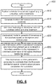
- Referring now to
FIG. 6 , amethod 400 is shown for determining physical parameters of the substrate using the learned model, the spectra generated by the optical metrology station and the mass generated by the mass metrology station. At 410, a substrate is positioned on a substrate support in the optical metrology station. At 414, the optical metrology system generates and stores location and spectra pairs for a substrate. At 424, the mass metrology system is used to determine the mass or mass change of the substrate before and after a substrate treatment. - At 432, the learned model generated during the training mode is used during production to convert the spectra at the measurement locations to thickness values or other parameters. At 436, the thicknesses at the measurement locations are used by the spatial thickness distribution module to determine parameters of the spatial thickness distribution model of the top surface of the substrate. The mass or mass change measurement is used as a constraint or boundary condition during regression analysis. At 440, the thickness, spatial thickness distribution model or other parameters are used to adjust process parameters.
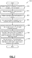
- Referring now to
FIG. 7 , amethod 500 is shown for determining physical parameters of the substrate using the learned model, the spectra generated by the optical metrology station and the mass generated by the mass metrology station. At 510, a substrate is positioned on a substrate support in the optical metrology station. At 514, the optical metrology system generates and stores location and spectra pairs for a substrate. At 520, principal component analysis is performed on the spectra. At 524, the mass metrology system is used to determine the mass or mass change of the substrate before and after a substrate treatment. - At 528, the learned model generated during the training mode is used during production to convert the principal component analysis to thickness values or other parameters. At 536, the thicknesses at the measurement locations are used by the spatial thickness distribution module to determine parameters of the spatial thickness distribution model of the top surface of the substrate. The mass or mass change measurement is used as a constraint or boundary condition during regression analysis. At 540, the thickness, spatial thickness distribution model or other parameters are used to adjust process parameters.
- Spatial and functional relationships between elements (for example, between modules, circuit elements, semiconductor layers, etc.) are described using various terms, including "connected," "engaged," "coupled," "adjacent," "next to," "on top of," "above," "below," and "disposed." Unless explicitly described as being "direct," when a relationship between first and second elements is described in the above disclosure, that relationship can be a direct relationship where no other intervening elements are present between the first and second elements, but can also be an indirect relationship where one or more intervening elements are present (either spatially or functionally) between the first and second elements. As used herein, the phrase at least one of A, B, and C should be construed to mean a logical (A OR B OR C), using a non-exclusive logical OR, and should not be construed to mean "at least one of A, at least one of B, and at least one of C."
- According to the invention, a controller is part of the metrology system. Such systems can comprise semiconductor processing equipment, including a processing tool or tools, chamber or chambers, a platform or platforms for processing, and/or specific processing components (a wafer pedestal, a gas flow system, etc.). These systems may be integrated with electronics for controlling their operation before, during, and after processing of a semiconductor wafer or substrate. The electronics may be referred to as the "controller," which may control various components or subparts of the system or systems. The controller, depending on the processing requirements and/or the type of system, may be programmed to control any of the processes disclosed herein, including the delivery of processing gases, temperature settings (e.g., heating and/or cooling), pressure settings, vacuum settings, power settings, radio frequency (RF) generator settings, RF matching circuit settings, frequency settings, flow rate settings, fluid delivery settings, positional and operation settings, wafer transfers into and out of a tool and other transfer tools and/or load locks connected to or interfaced with a specific system.
- Broadly speaking, the controller may be defined as electronics having various integrated circuits, logic, memory, and/or software that receive instructions, issue instructions, control operation, enable cleaning operations, enable endpoint measurements, and the like. The integrated circuits may include chips in the form of firmware that store program instructions, digital signal processors (DSPs), chips defined as application specific integrated circuits (ASICs), and/or one or more microprocessors, or microcontrollers that execute program instructions (e.g., software). Program instructions may be instructions communicated to the controller in the form of various individual settings (or program files), defining operational parameters for carrying out a particular process on or for a semiconductor wafer or to a system. The operational parameters may, in some embodiments, be part of a recipe defined by process engineers to accomplish one or more processing steps during the fabrication of one or more layers, materials, metals, oxides, silicon, silicon dioxide, surfaces, circuits, and/or dies of a wafer.
- The controller, in some implementations, may be a part of or coupled to a computer that is integrated with the system, coupled to the system, otherwise networked to the system, or a combination thereof. For example, the controller may be in the "cloud" or all or a part of a fab host computer system, which can allow for remote access of the wafer processing. The computer may enable remote access to the system to monitor current progress of fabrication operations, examine a history of past fabrication operations, examine trends or performance metrics from a plurality of fabrication operations, to change parameters of current processing, to set processing steps to follow a current processing, or to start a new process. In some examples, a remote computer (e.g. a server) can provide process recipes to a system over a network, which may include a local network or the Internet. The remote computer may include a user interface that enables entry or programming of parameters and/or settings, which are then communicated to the system from the remote computer. In some examples, the controller receives instructions in the form of data, which specify parameters for each of the processing steps to be performed during one or more operations. It should be understood that the parameters may be specific to the type of process to be performed and the type of tool that the controller is configured to interface with or control. Thus as described above, the controller may be distributed, such as by comprising one or more discrete controllers that are networked together and working towards a common purpose, such as the processes and controls described herein. An example of a distributed controller for such purposes would be one or more integrated circuits on a chamber in communication with one or more integrated circuits located remotely (such as at the platform level or as part of a remote computer) that combine to control a process on the chamber.
- Without limitation, example systems may include a plasma etch chamber or module, a deposition chamber or module, a spin-rinse chamber or module, a metal plating chamber or module, a clean chamber or module, a bevel edge etch chamber or module, a physical vapor deposition (PVD) chamber or module, a chemical vapor deposition (CVD) chamber or module, an atomic layer deposition (ALD) chamber or module, an atomic layer etch (ALE) chamber or module, an ion implantation chamber or module, a track chamber or module, and any other semiconductor processing systems that may be associated or used in the fabrication and/or manufacturing of semiconductor wafers.
- As noted above, depending on the process step or steps to be performed by the tool, the controller might communicate with one or more of other tool circuits or modules, other tool components, cluster tools, other tool interfaces, adjacent tools, neighboring tools, tools located throughout a factory, a main computer, another controller, or tools used in material transport that bring containers of wafers to and from tool locations and/or load ports in a semiconductor manufacturing factory.
Claims (17)
- A metrology system (100, 300) for substrate processing, comprising:an optical metrology station (126) including:a plurality of optical sensors (136) to perform measurements from a plurality of measurement locations on a substrate (114):a plurality of fiber cables (138) connected to the plurality of optical sensors (136); anda spectrometer (150) selectively connected to the plurality of fiber cables (138) to generate spectra at the plurality of measurement locations;a mass metrology station (310) to measure at least one of a mass or mass change of the substrate; anda controller (154) including:a modelling module (162) to generate thickness values at the plurality of measurement locations based on the spectra from the plurality of measurement locations and a learned model used to convert the spectra into the thickness values, wherein the learned model is generated using machine learning; anda spatial modelling module (170) to generate a spatial thickness distribution model of a surface of the substrate based on a known density of a layer added or removed to or from the substrate, and based on the thickness values at the plurality of measurement locations from the modelling module and the at least one of the mass or the mass change from the mass metrology station, the mass or mass change being used by the spatial modelling module as a constraint or boundary condition for regressionanalysis for the spatial distribution model, whereby the resulting spatial thickness distribution model of the substrate surface is used to determine the thickness of the top surface of the substrate at locations other than the measurement locations.
- The metrology system of claim 1, further comprising a plurality of shutters (142) connected to the plurality of fiber cables (138), respectively, wherein the plurality of shutters are configured to sequentially output spectra from one of the plurality of fiber cables at a time to the spectrometer.
- The metrology system of claim 1, wherein the machine learning includes a supervised learning model selected from a group consisting of linear models, support vector machine models, decision tree models, random forest models and Gaussian models.
- The metrology system of claim 1, wherein the learned model is based on a first-principle model.
- The metrology system of claim 4, wherein the first-principle model is selected from a group consisting of Fresnel multi-beam interference, rigorous coupled-wave analysis (RCWA), or finite-difference time-domain (FDTD).
- The metrology system of claim 1 wherein the substrate includes a plurality of dies and wherein the optical sensors have a beam diameter that generates samples from portions of a plurality of contiguous dies.
- The metrology system of claim 1, wherein the learned model is generated by correlating the spectra from a plurality of measurement locations of a plurality of sample substrates with at least one of thickness data, critical dimension data, depth data and material density data generated by a standalone metrology station (110) for the plurality ofmeasurement locations for the plurality of sample substrates; orwherein the learned model is generated by performing principal component analysis; orwherein the learned model is generated using an autoencoder.
- The metrology system of claim 1, further comprising an optical sensor positionerto adjust a position of at least one of the optical sensors; orfurther comprising a substrate support positioner to adjust a position of the substrate support.
- The metrology system of claim 1, wherein the plurality of optical sensors are configured to measurespectra from opposing surfaces of the substrate; orwherein the spatial modelling module generates the spatial thickness distribution model for the substrate further based a thickness of the substrate prior to film treatment.
- A method for providing metrology for substrate processing, comprising:
providing an optical metrology station (126) including a plurality of optical sensors (136) to measure spectra from a plurality of measurement locations on a substrate:measuring at least one of a mass or mass change of the substrate (114);generating thickness values at the plurality of measurement locations of the substrate based on the spectra from the plurality of measurement locations and a learned model used to convert the spectra into the thickness values, wherein the learned model is generated using machine learning;generating a spatial thickness distribution model of a surface the substrate based on a known density of a layer added or removed to or from the substrate, and based on the thickness values at the plurality of measurement locations and the at least one of the mass or the mass change; andusing the at least one of the mass or the mass change as at least one of a constraint or a boundary condition during regression analysis for the spatial thickness distribution model, whereby the resulting spatial thickness distribution model of the substrate surface is used to determine the thickness of the top surface of the substrate at locations other than the measurement locations. - The method of claim 10, wherein the machine learning includes a supervised learning model selected from a group consisting of linear models, support vector machine models, decision tree models, random forest models and Gaussian models.
- The method of claim 10, wherein the learned model is based on a first-principle model, wherein the first-principle model may be selected from a group consisting of Fresnel multi-beam interference, rigorous coupled-wave analysis (RCWA), or finite-difference time-domain (FDTD).
- The method of claim 10, wherein the substrate includes a plurality of dies and wherein the optical sensors have a beam diameter sufficient to generate samples from portions of a plurality of contiguous dies.
- The method of claim 10, further comprising generating the learned model by correlating the spectra from a plurality of measurement locations of a plurality of sample substrates with at least one of thickness data, critical dimension data, depth data and material density data generated by a standalone metrology station (110) for the plurality ofmeasurement locations for the plurality of sample substrates; orfurther comprising generating the learned model by performing principal component analysis; orfurther comprising generating the learned model using autoencoding.
- The method of claim 10 further comprising adjusting a position of at least one ofthe optical sensors during measurement of the spectra for the substrate; orfurther comprising adjusting a position of a substrate support supporting the substrate during measurement of the spectra for the substrate.
- The method of claim 10, wherein spectra are measured from opposing surfaces of the substrate.
- The method of claim 10, further comprising:generating a thickness of the substrate prior to film treatment; andgenerating the spatial thickness distribution model for the substrate further based the thickness of the substrate prior to film treatment.
Applications Claiming Priority (2)
| Application Number | Priority Date | Filing Date | Title |
|---|---|---|---|
| US15/696,768 US10989652B2 (en) | 2017-09-06 | 2017-09-06 | Systems and methods for combining optical metrology with mass metrology |
| PCT/US2018/049192 WO2019050801A1 (en) | 2017-09-06 | 2018-08-31 | Systems and methods for combining optical metrology with mass metrology |
Publications (3)
| Publication Number | Publication Date |
|---|---|
| EP3679598A1 EP3679598A1 (en) | 2020-07-15 |
| EP3679598A4 EP3679598A4 (en) | 2021-05-05 |
| EP3679598B1 true EP3679598B1 (en) | 2022-07-20 |
Family
ID=65517215
Family Applications (1)
| Application Number | Title | Priority Date | Filing Date |
|---|---|---|---|
| EP18854360.7A Active EP3679598B1 (en) | 2017-09-06 | 2018-08-31 | Systems and methods for combining optical metrology with mass metrology |
Country Status (8)
| Country | Link |
|---|---|
| US (1) | US10989652B2 (en) |
| EP (1) | EP3679598B1 (en) |
| JP (1) | JP7274460B2 (en) |
| KR (1) | KR102609122B1 (en) |
| CN (1) | CN111066131A (en) |
| IL (1) | IL273081B2 (en) |
| TW (1) | TWI782082B (en) |
| WO (1) | WO2019050801A1 (en) |
Families Citing this family (11)
| Publication number | Priority date | Publication date | Assignee | Title |
|---|---|---|---|---|
| US20220254666A1 (en) * | 2019-07-26 | 2022-08-11 | Lam Research Corporation | Integrated adaptive positioning systems and routines for automated wafer-handling robot teach and health check |
| WO2021030833A1 (en) * | 2019-08-09 | 2021-02-18 | Lam Research Corporation | Model based control of wafer non-uniformity |
| DE102020100565A1 (en) * | 2020-01-13 | 2021-07-15 | Aixtron Se | Process for depositing layers |
| US11353364B2 (en) | 2020-03-02 | 2022-06-07 | Lam Research Corporation | Thermal imaging for within wafer variability feedforward or feedback information |
| US20210408235A1 (en) * | 2020-06-25 | 2021-12-30 | Taiwan Semiconductor Manufacturing Co., Ltd. | Semiconductor device with silicide gate fill structure |
| WO2022005916A1 (en) * | 2020-06-29 | 2022-01-06 | Applied Materials, Inc. | Film thickness estimation from machine learning based processing of substrate images |
| US20220165593A1 (en) * | 2020-11-24 | 2022-05-26 | Applied Materials, Inc. | Feedforward control of multi-layer stacks during device fabrication |
| TWI773034B (en) * | 2020-12-18 | 2022-08-01 | 日月光半導體製造股份有限公司 | Systems and methods of monitoring apparatus |
| US11709477B2 (en) | 2021-01-06 | 2023-07-25 | Applied Materials, Inc. | Autonomous substrate processing system |
| US11881436B2 (en) * | 2021-07-07 | 2024-01-23 | Applied Materials, Inc. | Pre and post processing metrology apparatus |
| US20230169643A1 (en) * | 2021-11-30 | 2023-06-01 | Applied Materials, Inc. | Monitoring of deposited or etched film thickness using image-based mass distribution metrology |
Family Cites Families (27)
| Publication number | Priority date | Publication date | Assignee | Title |
|---|---|---|---|---|
| US5018007A (en) * | 1989-08-04 | 1991-05-21 | Universal Applied Sciences Inc. | Thin projection screen having a liquid crystal display screen overlaid a sheet of fiber optic cables |
| US5900633A (en) * | 1997-12-15 | 1999-05-04 | On-Line Technologies, Inc | Spectrometric method for analysis of film thickness and composition on a patterned sample |
| TW428079B (en) * | 1998-12-24 | 2001-04-01 | Sharp Kk | Thickness measurement apparatus of thin film using light interference method |
| US6791310B2 (en) | 1999-03-15 | 2004-09-14 | Therma-Wave, Inc. | Systems and methods for improved metrology using combined optical and electrical measurements |
| US6284986B1 (en) | 1999-03-15 | 2001-09-04 | Seh America, Inc. | Method of determining the thickness of a layer on a silicon substrate |
| IL130874A (en) * | 1999-07-09 | 2002-12-01 | Nova Measuring Instr Ltd | System and method for measuring patterned structures |
| US6694284B1 (en) | 2000-09-20 | 2004-02-17 | Kla-Tencor Technologies Corp. | Methods and systems for determining at least four properties of a specimen |
| US6826347B2 (en) * | 2001-07-12 | 2004-11-30 | Ngk Insulators, Ltd. | Two-dimensional optical element array and two-dimensional waveguide apparatus |
| US6940592B2 (en) | 2001-10-09 | 2005-09-06 | Applied Materials, Inc. | Calibration as well as measurement on the same workpiece during fabrication |
| US6678055B2 (en) * | 2001-11-26 | 2004-01-13 | Tevet Process Control Technologies Ltd. | Method and apparatus for measuring stress in semiconductor wafers |
| US7005306B1 (en) * | 2003-07-11 | 2006-02-28 | Nanometrics Incorporated | Accurate thickness measurement of thin conductive film |
| US20050020073A1 (en) | 2003-07-22 | 2005-01-27 | Lam Research Corporation | Method and system for electronic spatial filtering of spectral reflectometer optical signals |
| JP2007040930A (en) * | 2005-08-05 | 2007-02-15 | Ebara Corp | Film thickness measurement method, and substrate treatment device |
| US20070249071A1 (en) * | 2006-04-21 | 2007-10-25 | Lei Lian | Neural Network Methods and Apparatuses for Monitoring Substrate Processing |
| GB0719460D0 (en) | 2007-10-04 | 2007-11-14 | Metryx Ltd | Measurement apparatus and method |
| JP5681452B2 (en) * | 2010-11-08 | 2015-03-11 | 株式会社ディスコ | Measuring method and measuring device |
| US8577820B2 (en) | 2011-03-04 | 2013-11-05 | Tokyo Electron Limited | Accurate and fast neural network training for library-based critical dimension (CD) metrology |
| JP5660026B2 (en) * | 2011-12-28 | 2015-01-28 | 信越半導体株式会社 | Film thickness distribution measurement method |
| US20130203188A1 (en) | 2012-02-03 | 2013-08-08 | Globalfoundries Inc. | Hybrid metrology for semiconductor devices |
| US9330985B2 (en) | 2012-03-13 | 2016-05-03 | GlobalFoundries, Inc. | Automated hybrid metrology for semiconductor device fabrication |
| US20140333936A1 (en) * | 2013-05-10 | 2014-11-13 | Industrial Technology Research Institute | Thickness measuring system and method for a bonding layer |
| JP6293519B2 (en) * | 2014-03-05 | 2018-03-14 | 株式会社荏原製作所 | Polishing apparatus and polishing method |
| US10152678B2 (en) | 2014-11-19 | 2018-12-11 | Kla-Tencor Corporation | System, method and computer program product for combining raw data from multiple metrology tools |
| KR102125284B1 (en) * | 2015-03-11 | 2020-07-08 | 에이에스엠엘 네델란즈 비.브이. | Methods and devices for inspection and measurement |
| US9831110B2 (en) | 2015-07-30 | 2017-11-28 | Lam Research Corporation | Vision-based wafer notch position measurement |
| US10030971B2 (en) * | 2015-08-04 | 2018-07-24 | GlobalFoundries, Inc. | Measurement system and method for measuring in thin films |
| US10236222B2 (en) * | 2017-02-08 | 2019-03-19 | Kla-Tencor Corporation | System and method for measuring substrate and film thickness distribution |
-
2017
- 2017-09-06 US US15/696,768 patent/US10989652B2/en active Active
-
2018
- 2018-08-31 WO PCT/US2018/049192 patent/WO2019050801A1/en unknown
- 2018-08-31 CN CN201880057888.9A patent/CN111066131A/en active Pending
- 2018-08-31 KR KR1020207009665A patent/KR102609122B1/en active IP Right Grant
- 2018-08-31 EP EP18854360.7A patent/EP3679598B1/en active Active
- 2018-08-31 JP JP2020513515A patent/JP7274460B2/en active Active
- 2018-09-03 TW TW107130808A patent/TWI782082B/en active
-
2020
- 2020-03-05 IL IL273081A patent/IL273081B2/en unknown
Also Published As
| Publication number | Publication date |
|---|---|
| JP7274460B2 (en) | 2023-05-16 |
| KR102609122B1 (en) | 2023-12-01 |
| JP2020533787A (en) | 2020-11-19 |
| TW201928285A (en) | 2019-07-16 |
| EP3679598A4 (en) | 2021-05-05 |
| US20190072482A1 (en) | 2019-03-07 |
| IL273081B1 (en) | 2023-04-01 |
| US10989652B2 (en) | 2021-04-27 |
| KR20200040309A (en) | 2020-04-17 |
| IL273081B2 (en) | 2023-08-01 |
| CN111066131A (en) | 2020-04-24 |
| IL273081A (en) | 2020-04-30 |
| WO2019050801A1 (en) | 2019-03-14 |
| TWI782082B (en) | 2022-11-01 |
| EP3679598A1 (en) | 2020-07-15 |
Similar Documents
| Publication | Publication Date | Title |
|---|---|---|
| EP3679598B1 (en) | Systems and methods for combining optical metrology with mass metrology | |
| US7531368B2 (en) | In-line lithography and etch system | |
| US7373216B1 (en) | Method and apparatus for verifying a site-dependent wafer | |
| US20220344184A1 (en) | Systems and methods for autonomous process control and optimization of semiconductor equipment using light interferometry and reflectometry | |
| US11353364B2 (en) | Thermal imaging for within wafer variability feedforward or feedback information | |
| US7596423B2 (en) | Method and apparatus for verifying a site-dependent procedure | |
| US7650200B2 (en) | Method and apparatus for creating a site-dependent evaluation library | |
| WO2021030833A1 (en) | Model based control of wafer non-uniformity | |
| TW202230062A (en) | Autonomous substrate processing system | |
| US20240096713A1 (en) | Machine-learning in multi-step semiconductor fabrication processes | |
| TWI381468B (en) | In-line lithography and etch system | |
| US7783374B2 (en) | Method and apparatus for performing a site-dependent dual damascene procedure | |
| US20220334554A1 (en) | Large spot spectral sensing to control spatial setpoints | |
| TW202331889A (en) | Integrated substrate measurement system | |
| US7935545B2 (en) | Method and apparatus for performing a site-dependent dual patterning procedure | |
| US20240069537A1 (en) | Substrate placement optimization using substrate measurements | |
| US20240071838A1 (en) | Substrate placement optimization using substrate measurements | |
| US20230236583A1 (en) | Chamber component condition estimation using substrate measurements | |
| CN116583938A (en) | Machine learning in a multi-step semiconductor manufacturing process | |
| TW202330377A (en) | Methods and mechanisms for coupling sensors to transfer chamber robot |
Legal Events
| Date | Code | Title | Description |
|---|---|---|---|
| STAA | Information on the status of an ep patent application or granted ep patent |
Free format text: STATUS: THE INTERNATIONAL PUBLICATION HAS BEEN MADE |
|
| PUAI | Public reference made under article 153(3) epc to a published international application that has entered the european phase |
Free format text: ORIGINAL CODE: 0009012 |
|
| STAA | Information on the status of an ep patent application or granted ep patent |
Free format text: STATUS: REQUEST FOR EXAMINATION WAS MADE |
|
| 17P | Request for examination filed |
Effective date: 20200304 |
|
| AK | Designated contracting states |
Kind code of ref document: A1 Designated state(s): AL AT BE BG CH CY CZ DE DK EE ES FI FR GB GR HR HU IE IS IT LI LT LU LV MC MK MT NL NO PL PT RO RS SE SI SK SM TR |
|
| AX | Request for extension of the european patent |
Extension state: BA ME |
|
| DAV | Request for validation of the european patent (deleted) | ||
| DAX | Request for extension of the european patent (deleted) | ||
| A4 | Supplementary search report drawn up and despatched |
Effective date: 20210409 |
|
| RIC1 | Information provided on ipc code assigned before grant |
Ipc: G01B 11/06 20060101AFI20210401BHEP Ipc: G06N 20/10 20190101ALI20210401BHEP Ipc: G06N 20/20 20190101ALI20210401BHEP |
|
| REG | Reference to a national code |
Ref country code: DE Ref legal event code: R079 Ref document number: 602018038284 Country of ref document: DE Free format text: PREVIOUS MAIN CLASS: H01L0021660000 Ipc: G01B0011060000 |
|
| RIC1 | Information provided on ipc code assigned before grant |
Ipc: G06N 7/00 20060101ALI20211213BHEP Ipc: G06N 20/20 20190101ALI20211213BHEP Ipc: G06N 20/10 20190101ALI20211213BHEP Ipc: G01B 11/06 20060101AFI20211213BHEP |
|
| GRAP | Despatch of communication of intention to grant a patent |
Free format text: ORIGINAL CODE: EPIDOSNIGR1 |
|
| STAA | Information on the status of an ep patent application or granted ep patent |
Free format text: STATUS: GRANT OF PATENT IS INTENDED |
|
| INTG | Intention to grant announced |
Effective date: 20220204 |
|
| GRAS | Grant fee paid |
Free format text: ORIGINAL CODE: EPIDOSNIGR3 |
|
| GRAA | (expected) grant |
Free format text: ORIGINAL CODE: 0009210 |
|
| STAA | Information on the status of an ep patent application or granted ep patent |
Free format text: STATUS: THE PATENT HAS BEEN GRANTED |
|
| AK | Designated contracting states |
Kind code of ref document: B1 Designated state(s): AL AT BE BG CH CY CZ DE DK EE ES FI FR GB GR HR HU IE IS IT LI LT LU LV MC MK MT NL NO PL PT RO RS SE SI SK SM TR |
|
| REG | Reference to a national code |
Ref country code: CH Ref legal event code: EP |
|
| REG | Reference to a national code |
Ref country code: DE Ref legal event code: R096 Ref document number: 602018038284 Country of ref document: DE |
|
| REG | Reference to a national code |
Ref country code: AT Ref legal event code: REF Ref document number: 1505778 Country of ref document: AT Kind code of ref document: T Effective date: 20220815 |
|
| REG | Reference to a national code |
Ref country code: IE Ref legal event code: FG4D |
|
| REG | Reference to a national code |
Ref country code: LT Ref legal event code: MG9D |
|
| REG | Reference to a national code |
Ref country code: NL Ref legal event code: MP Effective date: 20220720 |
|
| PG25 | Lapsed in a contracting state [announced via postgrant information from national office to epo] |
Ref country code: SE Free format text: LAPSE BECAUSE OF FAILURE TO SUBMIT A TRANSLATION OF THE DESCRIPTION OR TO PAY THE FEE WITHIN THE PRESCRIBED TIME-LIMIT Effective date: 20220720 Ref country code: RS Free format text: LAPSE BECAUSE OF FAILURE TO SUBMIT A TRANSLATION OF THE DESCRIPTION OR TO PAY THE FEE WITHIN THE PRESCRIBED TIME-LIMIT Effective date: 20220720 Ref country code: PT Free format text: LAPSE BECAUSE OF FAILURE TO SUBMIT A TRANSLATION OF THE DESCRIPTION OR TO PAY THE FEE WITHIN THE PRESCRIBED TIME-LIMIT Effective date: 20221121 Ref country code: NO Free format text: LAPSE BECAUSE OF FAILURE TO SUBMIT A TRANSLATION OF THE DESCRIPTION OR TO PAY THE FEE WITHIN THE PRESCRIBED TIME-LIMIT Effective date: 20221020 Ref country code: NL Free format text: LAPSE BECAUSE OF FAILURE TO SUBMIT A TRANSLATION OF THE DESCRIPTION OR TO PAY THE FEE WITHIN THE PRESCRIBED TIME-LIMIT Effective date: 20220720 Ref country code: LV Free format text: LAPSE BECAUSE OF FAILURE TO SUBMIT A TRANSLATION OF THE DESCRIPTION OR TO PAY THE FEE WITHIN THE PRESCRIBED TIME-LIMIT Effective date: 20220720 Ref country code: LT Free format text: LAPSE BECAUSE OF FAILURE TO SUBMIT A TRANSLATION OF THE DESCRIPTION OR TO PAY THE FEE WITHIN THE PRESCRIBED TIME-LIMIT Effective date: 20220720 Ref country code: FI Free format text: LAPSE BECAUSE OF FAILURE TO SUBMIT A TRANSLATION OF THE DESCRIPTION OR TO PAY THE FEE WITHIN THE PRESCRIBED TIME-LIMIT Effective date: 20220720 Ref country code: ES Free format text: LAPSE BECAUSE OF FAILURE TO SUBMIT A TRANSLATION OF THE DESCRIPTION OR TO PAY THE FEE WITHIN THE PRESCRIBED TIME-LIMIT Effective date: 20220720 |
|
| REG | Reference to a national code |
Ref country code: AT Ref legal event code: MK05 Ref document number: 1505778 Country of ref document: AT Kind code of ref document: T Effective date: 20220720 |
|
| PG25 | Lapsed in a contracting state [announced via postgrant information from national office to epo] |
Ref country code: PL Free format text: LAPSE BECAUSE OF FAILURE TO SUBMIT A TRANSLATION OF THE DESCRIPTION OR TO PAY THE FEE WITHIN THE PRESCRIBED TIME-LIMIT Effective date: 20220720 Ref country code: IS Free format text: LAPSE BECAUSE OF FAILURE TO SUBMIT A TRANSLATION OF THE DESCRIPTION OR TO PAY THE FEE WITHIN THE PRESCRIBED TIME-LIMIT Effective date: 20221120 Ref country code: HR Free format text: LAPSE BECAUSE OF FAILURE TO SUBMIT A TRANSLATION OF THE DESCRIPTION OR TO PAY THE FEE WITHIN THE PRESCRIBED TIME-LIMIT Effective date: 20220720 Ref country code: GR Free format text: LAPSE BECAUSE OF FAILURE TO SUBMIT A TRANSLATION OF THE DESCRIPTION OR TO PAY THE FEE WITHIN THE PRESCRIBED TIME-LIMIT Effective date: 20221021 |
|
| REG | Reference to a national code |
Ref country code: CH Ref legal event code: PL |
|
| REG | Reference to a national code |
Ref country code: DE Ref legal event code: R097 Ref document number: 602018038284 Country of ref document: DE |
|
| PG25 | Lapsed in a contracting state [announced via postgrant information from national office to epo] |
Ref country code: SM Free format text: LAPSE BECAUSE OF FAILURE TO SUBMIT A TRANSLATION OF THE DESCRIPTION OR TO PAY THE FEE WITHIN THE PRESCRIBED TIME-LIMIT Effective date: 20220720 Ref country code: RO Free format text: LAPSE BECAUSE OF FAILURE TO SUBMIT A TRANSLATION OF THE DESCRIPTION OR TO PAY THE FEE WITHIN THE PRESCRIBED TIME-LIMIT Effective date: 20220720 Ref country code: MC Free format text: LAPSE BECAUSE OF FAILURE TO SUBMIT A TRANSLATION OF THE DESCRIPTION OR TO PAY THE FEE WITHIN THE PRESCRIBED TIME-LIMIT Effective date: 20220720 Ref country code: LU Free format text: LAPSE BECAUSE OF NON-PAYMENT OF DUE FEES Effective date: 20220831 Ref country code: LI Free format text: LAPSE BECAUSE OF NON-PAYMENT OF DUE FEES Effective date: 20220831 Ref country code: DK Free format text: LAPSE BECAUSE OF FAILURE TO SUBMIT A TRANSLATION OF THE DESCRIPTION OR TO PAY THE FEE WITHIN THE PRESCRIBED TIME-LIMIT Effective date: 20220720 Ref country code: CZ Free format text: LAPSE BECAUSE OF FAILURE TO SUBMIT A TRANSLATION OF THE DESCRIPTION OR TO PAY THE FEE WITHIN THE PRESCRIBED TIME-LIMIT Effective date: 20220720 Ref country code: CH Free format text: LAPSE BECAUSE OF NON-PAYMENT OF DUE FEES Effective date: 20220831 Ref country code: AT Free format text: LAPSE BECAUSE OF FAILURE TO SUBMIT A TRANSLATION OF THE DESCRIPTION OR TO PAY THE FEE WITHIN THE PRESCRIBED TIME-LIMIT Effective date: 20220720 |
|
| REG | Reference to a national code |
Ref country code: BE Ref legal event code: MM Effective date: 20220831 |
|
| PLBE | No opposition filed within time limit |
Free format text: ORIGINAL CODE: 0009261 |
|
| STAA | Information on the status of an ep patent application or granted ep patent |
Free format text: STATUS: NO OPPOSITION FILED WITHIN TIME LIMIT |
|
| PG25 | Lapsed in a contracting state [announced via postgrant information from national office to epo] |
Ref country code: SK Free format text: LAPSE BECAUSE OF FAILURE TO SUBMIT A TRANSLATION OF THE DESCRIPTION OR TO PAY THE FEE WITHIN THE PRESCRIBED TIME-LIMIT Effective date: 20220720 Ref country code: EE Free format text: LAPSE BECAUSE OF FAILURE TO SUBMIT A TRANSLATION OF THE DESCRIPTION OR TO PAY THE FEE WITHIN THE PRESCRIBED TIME-LIMIT Effective date: 20220720 |
|
| 26N | No opposition filed |
Effective date: 20230421 |
|
| GBPC | Gb: european patent ceased through non-payment of renewal fee |
Effective date: 20221020 |
|
| PG25 | Lapsed in a contracting state [announced via postgrant information from national office to epo] |
Ref country code: AL Free format text: LAPSE BECAUSE OF FAILURE TO SUBMIT A TRANSLATION OF THE DESCRIPTION OR TO PAY THE FEE WITHIN THE PRESCRIBED TIME-LIMIT Effective date: 20220720 |
|
| PG25 | Lapsed in a contracting state [announced via postgrant information from national office to epo] |
Ref country code: IE Free format text: LAPSE BECAUSE OF NON-PAYMENT OF DUE FEES Effective date: 20220831 Ref country code: FR Free format text: LAPSE BECAUSE OF NON-PAYMENT OF DUE FEES Effective date: 20220920 |
|
| PG25 | Lapsed in a contracting state [announced via postgrant information from national office to epo] |
Ref country code: SI Free format text: LAPSE BECAUSE OF FAILURE TO SUBMIT A TRANSLATION OF THE DESCRIPTION OR TO PAY THE FEE WITHIN THE PRESCRIBED TIME-LIMIT Effective date: 20220720 |
|
| PG25 | Lapsed in a contracting state [announced via postgrant information from national office to epo] |
Ref country code: BE Free format text: LAPSE BECAUSE OF NON-PAYMENT OF DUE FEES Effective date: 20220831 |
|
| PG25 | Lapsed in a contracting state [announced via postgrant information from national office to epo] |
Ref country code: GB Free format text: LAPSE BECAUSE OF NON-PAYMENT OF DUE FEES Effective date: 20221020 |
|
| P01 | Opt-out of the competence of the unified patent court (upc) registered |
Effective date: 20231021 |
|
| PGFP | Annual fee paid to national office [announced via postgrant information from national office to epo] |
Ref country code: DE Payment date: 20230829 Year of fee payment: 6 |