EP3678120A1 - Pixel driving circuit, pixel structure and manufacturing method - Google Patents
Pixel driving circuit, pixel structure and manufacturing method Download PDFInfo
- Publication number
- EP3678120A1 EP3678120A1 EP18852156.1A EP18852156A EP3678120A1 EP 3678120 A1 EP3678120 A1 EP 3678120A1 EP 18852156 A EP18852156 A EP 18852156A EP 3678120 A1 EP3678120 A1 EP 3678120A1
- Authority
- EP
- European Patent Office
- Prior art keywords
- pixel
- gate electrode
- gate
- transistor
- switching
- Prior art date
- Legal status (The legal status is an assumption and is not a legal conclusion. Google has not performed a legal analysis and makes no representation as to the accuracy of the status listed.)
- Granted
Links
Images


Classifications
-
- G—PHYSICS
- G09—EDUCATION; CRYPTOGRAPHY; DISPLAY; ADVERTISING; SEALS
- G09G—ARRANGEMENTS OR CIRCUITS FOR CONTROL OF INDICATING DEVICES USING STATIC MEANS TO PRESENT VARIABLE INFORMATION
- G09G3/00—Control arrangements or circuits, of interest only in connection with visual indicators other than cathode-ray tubes
- G09G3/20—Control arrangements or circuits, of interest only in connection with visual indicators other than cathode-ray tubes for presentation of an assembly of a number of characters, e.g. a page, by composing the assembly by combination of individual elements arranged in a matrix no fixed position being assigned to or needed to be assigned to the individual characters or partial characters
- G09G3/22—Control arrangements or circuits, of interest only in connection with visual indicators other than cathode-ray tubes for presentation of an assembly of a number of characters, e.g. a page, by composing the assembly by combination of individual elements arranged in a matrix no fixed position being assigned to or needed to be assigned to the individual characters or partial characters using controlled light sources
- G09G3/30—Control arrangements or circuits, of interest only in connection with visual indicators other than cathode-ray tubes for presentation of an assembly of a number of characters, e.g. a page, by composing the assembly by combination of individual elements arranged in a matrix no fixed position being assigned to or needed to be assigned to the individual characters or partial characters using controlled light sources using electroluminescent panels
- G09G3/32—Control arrangements or circuits, of interest only in connection with visual indicators other than cathode-ray tubes for presentation of an assembly of a number of characters, e.g. a page, by composing the assembly by combination of individual elements arranged in a matrix no fixed position being assigned to or needed to be assigned to the individual characters or partial characters using controlled light sources using electroluminescent panels semiconductive, e.g. using light-emitting diodes [LED]
-
- G—PHYSICS
- G02—OPTICS
- G02F—OPTICAL DEVICES OR ARRANGEMENTS FOR THE CONTROL OF LIGHT BY MODIFICATION OF THE OPTICAL PROPERTIES OF THE MEDIA OF THE ELEMENTS INVOLVED THEREIN; NON-LINEAR OPTICS; FREQUENCY-CHANGING OF LIGHT; OPTICAL LOGIC ELEMENTS; OPTICAL ANALOGUE/DIGITAL CONVERTERS
- G02F1/00—Devices or arrangements for the control of the intensity, colour, phase, polarisation or direction of light arriving from an independent light source, e.g. switching, gating or modulating; Non-linear optics
- G02F1/01—Devices or arrangements for the control of the intensity, colour, phase, polarisation or direction of light arriving from an independent light source, e.g. switching, gating or modulating; Non-linear optics for the control of the intensity, phase, polarisation or colour
- G02F1/13—Devices or arrangements for the control of the intensity, colour, phase, polarisation or direction of light arriving from an independent light source, e.g. switching, gating or modulating; Non-linear optics for the control of the intensity, phase, polarisation or colour based on liquid crystals, e.g. single liquid crystal display cells
- G02F1/133—Constructional arrangements; Operation of liquid crystal cells; Circuit arrangements
-
- G—PHYSICS
- G09—EDUCATION; CRYPTOGRAPHY; DISPLAY; ADVERTISING; SEALS
- G09G—ARRANGEMENTS OR CIRCUITS FOR CONTROL OF INDICATING DEVICES USING STATIC MEANS TO PRESENT VARIABLE INFORMATION
- G09G3/00—Control arrangements or circuits, of interest only in connection with visual indicators other than cathode-ray tubes
- G09G3/20—Control arrangements or circuits, of interest only in connection with visual indicators other than cathode-ray tubes for presentation of an assembly of a number of characters, e.g. a page, by composing the assembly by combination of individual elements arranged in a matrix no fixed position being assigned to or needed to be assigned to the individual characters or partial characters
- G09G3/22—Control arrangements or circuits, of interest only in connection with visual indicators other than cathode-ray tubes for presentation of an assembly of a number of characters, e.g. a page, by composing the assembly by combination of individual elements arranged in a matrix no fixed position being assigned to or needed to be assigned to the individual characters or partial characters using controlled light sources
- G09G3/30—Control arrangements or circuits, of interest only in connection with visual indicators other than cathode-ray tubes for presentation of an assembly of a number of characters, e.g. a page, by composing the assembly by combination of individual elements arranged in a matrix no fixed position being assigned to or needed to be assigned to the individual characters or partial characters using controlled light sources using electroluminescent panels
- G09G3/32—Control arrangements or circuits, of interest only in connection with visual indicators other than cathode-ray tubes for presentation of an assembly of a number of characters, e.g. a page, by composing the assembly by combination of individual elements arranged in a matrix no fixed position being assigned to or needed to be assigned to the individual characters or partial characters using controlled light sources using electroluminescent panels semiconductive, e.g. using light-emitting diodes [LED]
- G09G3/3208—Control arrangements or circuits, of interest only in connection with visual indicators other than cathode-ray tubes for presentation of an assembly of a number of characters, e.g. a page, by composing the assembly by combination of individual elements arranged in a matrix no fixed position being assigned to or needed to be assigned to the individual characters or partial characters using controlled light sources using electroluminescent panels semiconductive, e.g. using light-emitting diodes [LED] organic, e.g. using organic light-emitting diodes [OLED]
- G09G3/3225—Control arrangements or circuits, of interest only in connection with visual indicators other than cathode-ray tubes for presentation of an assembly of a number of characters, e.g. a page, by composing the assembly by combination of individual elements arranged in a matrix no fixed position being assigned to or needed to be assigned to the individual characters or partial characters using controlled light sources using electroluminescent panels semiconductive, e.g. using light-emitting diodes [LED] organic, e.g. using organic light-emitting diodes [OLED] using an active matrix
- G09G3/3233—Control arrangements or circuits, of interest only in connection with visual indicators other than cathode-ray tubes for presentation of an assembly of a number of characters, e.g. a page, by composing the assembly by combination of individual elements arranged in a matrix no fixed position being assigned to or needed to be assigned to the individual characters or partial characters using controlled light sources using electroluminescent panels semiconductive, e.g. using light-emitting diodes [LED] organic, e.g. using organic light-emitting diodes [OLED] using an active matrix with pixel circuitry controlling the current through the light-emitting element
-
- G—PHYSICS
- G09—EDUCATION; CRYPTOGRAPHY; DISPLAY; ADVERTISING; SEALS
- G09G—ARRANGEMENTS OR CIRCUITS FOR CONTROL OF INDICATING DEVICES USING STATIC MEANS TO PRESENT VARIABLE INFORMATION
- G09G3/00—Control arrangements or circuits, of interest only in connection with visual indicators other than cathode-ray tubes
- G09G3/20—Control arrangements or circuits, of interest only in connection with visual indicators other than cathode-ray tubes for presentation of an assembly of a number of characters, e.g. a page, by composing the assembly by combination of individual elements arranged in a matrix no fixed position being assigned to or needed to be assigned to the individual characters or partial characters
- G09G3/22—Control arrangements or circuits, of interest only in connection with visual indicators other than cathode-ray tubes for presentation of an assembly of a number of characters, e.g. a page, by composing the assembly by combination of individual elements arranged in a matrix no fixed position being assigned to or needed to be assigned to the individual characters or partial characters using controlled light sources
- G09G3/30—Control arrangements or circuits, of interest only in connection with visual indicators other than cathode-ray tubes for presentation of an assembly of a number of characters, e.g. a page, by composing the assembly by combination of individual elements arranged in a matrix no fixed position being assigned to or needed to be assigned to the individual characters or partial characters using controlled light sources using electroluminescent panels
- G09G3/32—Control arrangements or circuits, of interest only in connection with visual indicators other than cathode-ray tubes for presentation of an assembly of a number of characters, e.g. a page, by composing the assembly by combination of individual elements arranged in a matrix no fixed position being assigned to or needed to be assigned to the individual characters or partial characters using controlled light sources using electroluminescent panels semiconductive, e.g. using light-emitting diodes [LED]
- G09G3/3208—Control arrangements or circuits, of interest only in connection with visual indicators other than cathode-ray tubes for presentation of an assembly of a number of characters, e.g. a page, by composing the assembly by combination of individual elements arranged in a matrix no fixed position being assigned to or needed to be assigned to the individual characters or partial characters using controlled light sources using electroluminescent panels semiconductive, e.g. using light-emitting diodes [LED] organic, e.g. using organic light-emitting diodes [OLED]
- G09G3/3266—Details of drivers for scan electrodes
-
- G—PHYSICS
- G09—EDUCATION; CRYPTOGRAPHY; DISPLAY; ADVERTISING; SEALS
- G09G—ARRANGEMENTS OR CIRCUITS FOR CONTROL OF INDICATING DEVICES USING STATIC MEANS TO PRESENT VARIABLE INFORMATION
- G09G3/00—Control arrangements or circuits, of interest only in connection with visual indicators other than cathode-ray tubes
- G09G3/20—Control arrangements or circuits, of interest only in connection with visual indicators other than cathode-ray tubes for presentation of an assembly of a number of characters, e.g. a page, by composing the assembly by combination of individual elements arranged in a matrix no fixed position being assigned to or needed to be assigned to the individual characters or partial characters
- G09G3/22—Control arrangements or circuits, of interest only in connection with visual indicators other than cathode-ray tubes for presentation of an assembly of a number of characters, e.g. a page, by composing the assembly by combination of individual elements arranged in a matrix no fixed position being assigned to or needed to be assigned to the individual characters or partial characters using controlled light sources
- G09G3/30—Control arrangements or circuits, of interest only in connection with visual indicators other than cathode-ray tubes for presentation of an assembly of a number of characters, e.g. a page, by composing the assembly by combination of individual elements arranged in a matrix no fixed position being assigned to or needed to be assigned to the individual characters or partial characters using controlled light sources using electroluminescent panels
- G09G3/32—Control arrangements or circuits, of interest only in connection with visual indicators other than cathode-ray tubes for presentation of an assembly of a number of characters, e.g. a page, by composing the assembly by combination of individual elements arranged in a matrix no fixed position being assigned to or needed to be assigned to the individual characters or partial characters using controlled light sources using electroluminescent panels semiconductive, e.g. using light-emitting diodes [LED]
- G09G3/3208—Control arrangements or circuits, of interest only in connection with visual indicators other than cathode-ray tubes for presentation of an assembly of a number of characters, e.g. a page, by composing the assembly by combination of individual elements arranged in a matrix no fixed position being assigned to or needed to be assigned to the individual characters or partial characters using controlled light sources using electroluminescent panels semiconductive, e.g. using light-emitting diodes [LED] organic, e.g. using organic light-emitting diodes [OLED]
- G09G3/3275—Details of drivers for data electrodes
-
- G—PHYSICS
- G09—EDUCATION; CRYPTOGRAPHY; DISPLAY; ADVERTISING; SEALS
- G09G—ARRANGEMENTS OR CIRCUITS FOR CONTROL OF INDICATING DEVICES USING STATIC MEANS TO PRESENT VARIABLE INFORMATION
- G09G2300/00—Aspects of the constitution of display devices
- G09G2300/04—Structural and physical details of display devices
- G09G2300/0421—Structural details of the set of electrodes
- G09G2300/0426—Layout of electrodes and connections
-
- G—PHYSICS
- G09—EDUCATION; CRYPTOGRAPHY; DISPLAY; ADVERTISING; SEALS
- G09G—ARRANGEMENTS OR CIRCUITS FOR CONTROL OF INDICATING DEVICES USING STATIC MEANS TO PRESENT VARIABLE INFORMATION
- G09G2300/00—Aspects of the constitution of display devices
- G09G2300/04—Structural and physical details of display devices
- G09G2300/0439—Pixel structures
- G09G2300/0465—Improved aperture ratio, e.g. by size reduction of the pixel circuit, e.g. for improving the pixel density or the maximum displayable luminance or brightness
-
- G—PHYSICS
- G09—EDUCATION; CRYPTOGRAPHY; DISPLAY; ADVERTISING; SEALS
- G09G—ARRANGEMENTS OR CIRCUITS FOR CONTROL OF INDICATING DEVICES USING STATIC MEANS TO PRESENT VARIABLE INFORMATION
- G09G2300/00—Aspects of the constitution of display devices
- G09G2300/08—Active matrix structure, i.e. with use of active elements, inclusive of non-linear two terminal elements, in the pixels together with light emitting or modulating elements
- G09G2300/0809—Several active elements per pixel in active matrix panels
-
- G—PHYSICS
- G09—EDUCATION; CRYPTOGRAPHY; DISPLAY; ADVERTISING; SEALS
- G09G—ARRANGEMENTS OR CIRCUITS FOR CONTROL OF INDICATING DEVICES USING STATIC MEANS TO PRESENT VARIABLE INFORMATION
- G09G2320/00—Control of display operating conditions
- G09G2320/02—Improving the quality of display appearance
- G09G2320/0209—Crosstalk reduction, i.e. to reduce direct or indirect influences of signals directed to a certain pixel of the displayed image on other pixels of said image, inclusive of influences affecting pixels in different frames or fields or sub-images which constitute a same image, e.g. left and right images of a stereoscopic display
Definitions
- the present invention relates to the field of display screen display technology, and particularly to a pixel driving circuit, a pixel structure, and a manufacturing method thereof suitable for high pixel density.
- a pixel (or a sub-pixel) is usually composed of a transistor driving circuit and a luminescent material, and the size of the transistor driving circuit needs to be further reduced in order to increase the PPI.
- the embodiments of the present invention provide a pixel driving circuit, a pixel structure, and a pixel manufacturing method which are suitable for high pixel density, to solve technical problems that a pixel of anexisting panel isaffected by a pixel driving circuit and the pixel density is too low.
- a pixel driving circuit suitable for high pixel density of the present invention includes a switching transistor comprising a dual gate field effect transistor.
- the dual gate field effect transistor includes a first gate electrode and a second gate electrode, and the first gate electrode and the second gate electrode are connected to a same scan line.
- an input end of the switching transistor is a sourceelectrode, and an output end of the switching transistor is a drain electrode.
- the first gate electrode and the second gate electrode are of a top gate type, or the first gate electrode and the second gate electrode are of a bottom gate type, or the first gate electrode is of a top gate type and the second gate electrode is of a bottom gate type, or the first gate electrode is of a bottom gate type and the second gate electrode is of a top gate type.
- a pixel structure suitable for high pixel density of the present invention includes a first pixel and a second pixel adjacent to the first pixel, the first pixel and the second pixel respectively including the pixel driving circuit suitable for high pixel density, input ends of the switching transistors in the first pixel and the second pixel are connected to the same data line.
- a first active region is defined between the first gateelectrode and the second gate electrode of the switching transistor of the first pixel, and a second active region is defined between the first gate electrode and the second gate electrode of the switching transistor of the second pixel, and the first active region and the second active region include a common portion.
- the pixel driving circuits of the first pixel and the second pixel are horizontally opposed to each other, and the switching transistors of the pixel driving circuit are adjacent to each other.
- each of the first pixel and the second pixel are arranged in a row, the corresponding first pixel and the second pixel corresponding to the first pixel are arranged in a column, the input ends of the switching transistors of the first pixel and the second pixel in the same column are connected to a same data line, and the first gate electrode and the second gate electrode of the switching transistors of the first pixelsin the same row or the second pixelsin the same row are connected to the same scan line.
- the pixel driving circuit further includes a driving transistor and a holding capacitor, a drain electrode of the switching transistor is connected to a gate electrode of the driving transistor, a source electrode of the switching transistor is connected to the data line, and the driving transistor comprises a field effect transistor, a source electrode of the driving transistor is connected to a working voltage, and a drain electrode of the driving transistor is connected to a working ground.
- a method for manufacturing a pixel suitable for high pixel density of the present invention includes: forming an active layer.
- the forming the active layer includes:
- An embodiment of the inventionfurther includes: symmetrically forming patterns of the driving transistors in the pixel driving circuits of the adjacent pixels on both sides of the strip-shaped pattern, based on a direction of along sideof the strip-shaped pattern.
- the method further includes forming a first insulating layer and a first metal layer on the active layer, and forming a pattern of a scan line on the first metal layer, the dual gate field effect transistor including a first gate electrode and a second a gate electrode, the first gate electrode and the second gate electrode are connected to ascan line.
- the pixel driving circuit with high pixel density firstly, by means of adopting a dual gatefield effect transistor as a switching transistor, avoidingto use an additional compensation circuit to overcome the interference factor, which may cause pixel complexity and affect the improvement of PPI.
- the gates of the switching transistors of two adjacent pixels in the same column are connected in parallel and a part of the semiconductor crystal in the active region is shared,so that the structures of adjacent switching transistors are simplified to reduce the spacing betweenadjacent switching transistors, and thereby the spacing between adjacent pixels in the same column is reduced, and the pixel density is improved.
- FIG. 1 is a schematic diagram showing an equivalent circuit of a pixel driving circuit suitable for high pixel density according to an embodiment of the present invention.
- a pixel (or a single sub-pixel) is arranged in a row and a column, and the pixels of each row are connected to a same scan line, and the pixels of each column are connected to a same data line.
- FIG. 1 in an embodiment of the present invention, a pixel (or a single sub-pixel) is arranged in a row and a column, and the pixels of each row are connected to a same scan line, and the pixels of each column are connected to a same data line.
- pixels including a upper left pixel, a upper right pixel, a lower left pixel, and a lower right pixel.
- the upper left pixel and the upper right pixel, deemed as the first pixels, are connected to the scan line scan1
- the lower left pixel and the lower right pixel, deemed as the second pixels are connected to the scan line scan2
- the upper left pixel and the lower left pixel, deemed as adjacent first and second pixels are connected to the data line data1
- the upper right pixel and the lower right pixel, deemed as anotheradjacent first and second pixels are connected to the data line data2.
- a pixel structure in an embodiment of the present inventionas shown in FIG. 1 includes a pixel driving circuit and a light emitting diode (for example, an organic light emitting display made of indium tin oxide), and the pixel driving circuit adopts a 2T1C pixel driving circuit, which includes a switching transistor(for example, a Field Effect Transistor (FET)), a driving transistor(for example, a field effect transistor), and a holding capacitor, in which:
- FET Field Effect Transistor
- the drain electrode of the switching transistor is connected to the gate electrode of the driving transistor.
- the gate electrode of the switching transistor is connected to the scan line.
- the source electrode of the switching transistor is connected to the data line.
- the light emitting diode is connected in series with the source electrode or the drain electrode of the driving transistor.
- the holding capacitor is connected between the gate electrode and the source electrode of the driving transistor or between the gate electrode and the drainelectrode of the driving transistor, depending on the position of the series connection of the light emitting diode.
- the source electrode of the driving transistor is connected to a working voltage.
- the drain electrode of the driving transistor is connected to the working ground.
- a gate electrode of a switching transistor T2a is connected to a scan line scan1
- a source electrode of the switching transistor T2a is connected to a data line data1
- a drain electrode of the switching transistor T2a is connected to a gate electrode of a driving transistor T1a
- a source electrode of the driving transistor T1a is connected to the working voltage Vdd
- a drain electrode of the driving transistor T1a is connected in series with the LED, and then connected to the working ground Vss.
- switching transistors for example, switching transistors T2a, T2b, T4a, and T4b
- switching transistors T2a, T2b, T4a, and T4b of a pixel driving circuit according to an embodiment of the present inventionincludedual gate FETs, and a first gate electrode and a second gate electrode of a dual gate FET are connected to a same scan line.
- the first gate electrode g1 and the second gate electrode g2 included in the switching transistor T2a are connected to the scan line scan1.
- the gate electrodes of the switching transistor T2a and the switching transistor T2b in the same row are connected to the same scan line scan1.
- the first gate electrode g1 and the second gate electrode g2 of the dual gate field effect transistor are of a top gate type.
- the dual gate FETsadopted by the switching transistors of the pixel driving circuit of the same column of pixels have the same type of gate electrode.
- the first gate electrode g1 and the second gate electrode g2 of the dual gate field effect transistor are of a bottom gate type.
- the dual gate FETsadopted by the switching transistors of the pixel driving circuit of the same column of pixels have the same type of gate electrode.
- the first gate electrode g1 (or the second gate electrode g2) of the dual gate field effect transistor is of a top gate type
- the second gate electrode g2 (or the first gate electrode g1) is of a bottom gate type.
- the dual gate FETs adopted by the switching transistors of the pixel driving circuit of the same column of pixels have the same type of gate electrode.
- two rows of pixels are deemed as a group, and pixel driving circuits of a same column of pixels in the first row of pixels (the first pixels) and the second row of pixels (the second pixels) are horizontally opposed to each other.
- a common portion is formed between the first gate electrode and the second gate electrode of switching transistorsof the first pixels and the first gate electrode and the second gate electrode of switching transistors of the second pixel.
- "Horizontally opposed to each other” means that in the pixel driving circuits of the first pixel and the second pixel in the same column, the switching transistor and the driving transistor are located at the same level, and the switching transistor and the driving transistor are symmetrically arranged while the switching transistors are adjacent to each other.
- the switching transistor T2a in the pixel driving circuit of the upper left pixel and the switching transistor T4a in the pixel driving circuit of the lower left pixel includedual gate FETs, and an active region (a semiconductor of anactive layer) between the first gate electrode g1 and the second gate electrode g2 of the switching transistor T2a and an active region (a semiconductor of anactive layer) between the first gate electrode g1 and the second gate electrode g2 of the switching transistor T4aform common portions(the elliptical areas in FIG. 1 ).
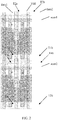
- FIG. 3 is a schematic structural diagram of a circuit layout suitable for a pixel structure with high pixel density according to an embodiment of the present invention. As shown in FIG. 3 , taking anupper left pixel (a first pixel) and alower left pixel (a second pixel) as an example, the semiconductor pattern portions of the gate electrodes of the switching transistor T2a and the switching transistor T4a are overlapped and common used, and the overlapping position forms a strip-shaped pattern T24.
- an OLED panel as a close-range display unit requires the arrangement of pixels to be as close as possible and the size of pixel driving circuits to be as small as possible, to increase the aperture ratio of the pixels.
- the increasing of pixel density causes(the area of) the light-emitting device of each pixel to be reduced, which causes the driving current of the light emitting device to be reduced.
- the driving transistor of the pixel driving circuit needs to be associated with the working voltage, the working ground and the light emitting device, and the channel length of the driving transistorbecomes even longer due to manufacturinglevel, so the control voltage of the gate electrode of the driving transistor needs to be more precise.
- the gate electrode of the driving transistor cannot be stably controlled. If the interference factors are overcome by addinga compensation circuit, it will affect the pixel density and reduce the pixel reliability.
- the pixel structure withhigh pixel density in the embodiments of the invention firstly uses the dual gate FET as the switching transistor to avoid excessive draincurrent (i.e., gate-drain current), and parasitic capacitances such as feedback capacitances are effectively overcome, so as to ensure the stability of the gate control current of the driving transistor.
- FIG. 2 is a schematic structural diagram of a circuit layout suitable for a pixel structure withhigh pixel density according to an embodiment of the present invention.
- the switching transistor T2a of the upper left pixel and the switching transistor T4a of the lower left pixel includedual gate FETs.
- the first gate electrode g1 and the second gate electrode g2 of the switching transistor T2a are connected to the same scan line, scan1, the first gate electrode g1 and the second gate electrode g2 of the switching transistor T4a are connected to the same scan line, scan2, and the source electrodes s of the switching transistor T2a and the switching transistor T4a are connected to the same data line data1.
- the driving transistor T1a of the upper left pixel is adjacent to the switching transistor T4a of the lower left pixel, a pixel pitch between the upper left pixel and the lower left pixel is therefore formed.
- the switching transistor uses a dual gate structure when the channel length of the driving transistor is longer than 16 ⁇ m and the minimum pixel pitchis 35.35 ⁇ m, the maximum PPI of pixelscan only be 719, which is unable to meet the requirements of some VR projects.
- the switching transistor T2a of the upper left pixel and the switching transistor T4a of the lower left pixel includedual gate FETs.
- the first field gate electrode g1 and the second gate electrode g2 of the switching transistor T2a are connected to the same scan line scan1
- the first gate electrode g1 and the second gate electrode g2 of the switching transistor T4a are connected to the same scan line scan2
- the source electrodes s of the switching transistor T2a and the switching transistor T4a are connected to the same data line data1.
- the pixel driving circuits of the upper left pixel and the lower left pixel in the same column and adjacent to each other are horizontally opposed to each other, the switching transistor T2a of the upper left pixel and the switching transistor T4a of the lower left pixel are adjacent to each other.
- the source electrode pattern and the drain electrode pattern,on the active layer, of the switching transistor T2a and the switching transistor T4a are partially overlapped, and a parallel connection between the source electrodes of the switching transistor T2a and the switching transistor T4a andaparallel connection between the drain electrodes of the switching transistor T2a and the switching transistor T4a are formed, so that the switching transistor is selected by means of the scanning line,and signals are input and output by means of the source electrodes and drain electrodes connected in parallel.
- the pixel structure with high pixel density of an embodiment of the present invention utilizes the partial overlapping of semiconductors of the switching transistors of two adjacent pixels in the same column to form parallel connections of input ends and parallel connections of output ends in each row, thereby simplifying the structures of the adjacent switching transistors to reduce the spacing between adjacent switching transistors. Further, the intervals between adjacent pixels in the same column are reduced, and the pixel density is improved.
- a dual gate structure being adopted by switching transistorswhen the channel length of the driving transistor is greater than 16 ⁇ m, the pixel spacing may be less than 35.35 ⁇ m, and the maximum PPI of pixelscan be made to 810, meeting the requirements of the VR projects.
- the main difference between the manufacturing method of the pixel structure with high pixel density according to the embodiments of the present invention and the conventional pixel manufacturing method lies in the manufacturing method of the adjacent switching transistors in the pixel driving circuits of two adjacent pixels in the same column.
- the two switching transistors have a common semiconductor region (i.e., the strip-shaped pattern T24), switching transistors of different pixels are selected by different scanning lines, and the strip-shaped pattern T24 may be applied to corresponding switching transistors.
- This type of switching transistor pattern simplifies the arrangement structures of the switching transistors in adjacent pixels in the same column, reduces the pattern size, and further reduces the pixel pitch.
- the manufacturing method of the pixel structure with high pixel density may simplify the fabrication of the (dual gate) switching transistor in the pixel driving circuit of two adjacent pixels, reduce the pixel pitch, and effectively improve the PPI.
- the pixel driving circuit, the pixel structure and the manufacturing method thereof avoid the adoption of the additional compensation circuit to overcome the interference factor,which causes the pixel complications, and the pixel structure is simplified, and the pixel density is improved. That may be widely used in industrial production.
Landscapes
- Engineering & Computer Science (AREA)
- Physics & Mathematics (AREA)
- General Physics & Mathematics (AREA)
- Theoretical Computer Science (AREA)
- Computer Hardware Design (AREA)
- Nonlinear Science (AREA)
- Crystallography & Structural Chemistry (AREA)
- Optics & Photonics (AREA)
- Chemical & Material Sciences (AREA)
- Mathematical Physics (AREA)
- Control Of Indicators Other Than Cathode Ray Tubes (AREA)
- Devices For Indicating Variable Information By Combining Individual Elements (AREA)
- Electroluminescent Light Sources (AREA)
- Control Of El Displays (AREA)
Abstract
Description
- The present invention claims priority to Chinese patent application No.
2017107604720 filed on Aug. 29, 2017 - The present inventionrelates to the field of display screen display technology, and particularly to a pixel driving circuit, a pixel structure, and a manufacturing method thereof suitable for high pixel density.
- With the development of Virtual Reality (VR) technology, a requirement on the Pixel PerInch(PPI) ofa display panel has also gradually increased. A pixel (or a sub-pixel) is usually composed of a transistor driving circuit and a luminescent material, and the size of the transistor driving circuit needs to be further reduced in order to increase the PPI.
- In view of the above, the embodiments of the present inventionprovide a pixel driving circuit, a pixel structure, and a pixel manufacturing method which are suitable for high pixel density, to solve technical problems that a pixel of anexisting panel isaffected by a pixel driving circuit and the pixel density is too low.
- A pixel driving circuit suitable for high pixel density of the present inventionincludes a switching transistor comprising a dual gate field effect transistor.The dual gate field effect transistor includes a first gate electrode and a second gate electrode, and the first gate electrode and the second gate electrode are connected to a same scan line.
- In an embodiment of the invention, an input end of the switching transistor is a sourceelectrode, and an output end of the switching transistor is a drain electrode.
- In an embodiment of the invention, the first gate electrode and the second gate electrode are of a top gate type, or the first gate electrode and the second gate electrode are of a bottom gate type, or the first gate electrode is of a top gate type and the second gate electrode is of a bottom gate type, or the first gate electrode is of a bottom gate type and the second gate electrode is of a top gate type.
- A pixel structure suitable for high pixel density of the present inventionincludes a first pixel and a second pixel adjacent to the first pixel, the first pixel and the second pixel respectively including the pixel driving circuit suitable for high pixel density, input ends of the switching transistors in the first pixel and the second pixel are connected to the same data line.
- In an embodiment of the invention, a first active region is defined between the first gateelectrode and the second gate electrode of the switching transistor of the first pixel, and a second active region is defined between the first gate electrode and the second gate electrode of the switching transistor of the second pixel, and the first active region and the second active region include a common portion.
- In an embodiment of the invention, the pixel driving circuits of the first pixel and the second pixel are horizontally opposed to each other, and the switching transistors of the pixel driving circuit are adjacent to each other.
- In an embodiment of the invention, each of the first pixel and the second pixel are arranged in a row, the corresponding first pixel and the second pixel corresponding to the first pixel are arranged in a column, the input ends of the switching transistors of the first pixel and the second pixel in the same column are connected to a same data line, and the first gate electrode and the second gate electrode of the switching transistors of the first pixelsin the same row or the second pixelsin the same row are connected to the same scan line.
- The pixel driving circuit further includes a driving transistor and a holding capacitor, a drain electrode of the switching transistor is connected to a gate electrode of the driving transistor, a source electrode of the switching transistor is connected to the data line, and the driving transistor comprises a field effect transistor, a source electrode of the driving transistor is connected to a working voltage, and a drain electrode of the driving transistor is connected to a working ground.
- A method for manufacturing a pixel suitable for high pixel density of the present inventionincludes: forming an active layer.The forming the active layer includes:
- forming a strip-shaped patternonthe active layer, as a common portion pattern of as witching transistor of a pixel driving circuits in adjacent pixels; and
- forming a pattern of a dual gatefield effect transistorextending toward one side of the strip-shaped patternalong a short side of the strip-shaped pattern at both ends of the strip-shaped pattern, and forming a pattern of another dual gate field effect transistorextending toward the other side of the strip-shaped pattern along the short side of the strip-shaped pattern at both ends of the strip-shaped pattern, patterns are used as patternsinthe switching transistors of the pixel driving circuits in the adjacent pixels respectively.
- An embodiment of the inventionfurther includes:
symmetrically forming patterns of the driving transistors in the pixel driving circuits of the adjacent pixels on both sides of the strip-shaped pattern, based on a direction of along sideof the strip-shaped pattern. - The method further includes forming a first insulating layer and a first metal layer on the active layer, and forming a pattern of a scan line on the first metal layer, the dual gate field effect transistor including a first gate electrode and a second a gate electrode, the first gate electrode and the second gate electrode are connected to ascan line.
- The pixel driving circuit with high pixel density according to the embodiments of the present invention, firstly, by means of adopting a dual gatefield effect transistor as a switching transistor, avoidingto use an additional compensation circuit to overcome the interference factor, which may cause pixel complexity and affect the improvement of PPI. In the pixel structure suitable for high pixel density, the gates of the switching transistors of two adjacent pixels in the same column are connected in parallel and a part of the semiconductor crystal in the active region is shared,so that the structures of adjacent switching transistors are simplified to reduce the spacing betweenadjacent switching transistors, and thereby the spacing between adjacent pixels in the same column is reduced, and the pixel density is improved.
- In order to illustrate technical solutions of embodiments of the present inventionor the technical solutions in the prior art more clearly, the accompanying drawings required in the embodiments or the descriptions of the prior art will be briefly described below. Obviously, the accompanying drawings in the following descriptions are some embodiments of the present invention, and those skilled in the art may obtain other drawings according to the accompanying drawings without creative efforts.
-
FIG. 1 is a schematic diagram showing an equivalent circuit of a pixel driving circuit suitable for high pixel density according to an embodiment of the present invention. -
FIG. 2 is a schematic structural diagram of a circuit layout suitable for a pixel structure withhigh pixel density according to an embodiment of the present invention. -
FIG. 3 is a schematic structural diagram of a circuit layout suitable for a pixel structure with high pixel density according to an embodiment of the present invention. - In order to render the purposes, technical solutions and advantages of the embodiments of the present invention more clearly, the technical solutions of the embodiments of the present invention are clearly and completely described in the following with reference to the accompanying drawings of the embodiments of the present invention. Obviously, the described embodiments are parts of the embodiments of the invention, and not all of the embodiments. Based on the embodiments of the present invention, other embodiments obtained by those skilled in the art without creative efforts are within the scope of the present invention.
-
FIG. 1 is a schematic diagram showing an equivalent circuit of a pixel driving circuit suitable for high pixel density according to an embodiment of the present invention. As shown inFIG. 1 , in an embodiment of the present invention, a pixel (or a single sub-pixel) is arranged in a row and a column, and the pixels of each row are connected to a same scan line, and the pixels of each column are connected to a same data line. As shown inFIG. 1 ,four pixels including a upper left pixel, a upper right pixel, a lower left pixel, and a lower right pixel.The upper left pixel and the upper right pixel, deemed as the first pixels, are connected to the scan line scan1, and the lower left pixel and the lower right pixel, deemed as the second pixels, are connected to the scan line scan2, and the upper left pixel and the lower left pixel, deemed as adjacent first and second pixels, are connected to the data line data1, and the upper right pixel and the lower right pixel, deemed as anotheradjacent first and second pixels, are connected to the data line data2. - A pixel structure in an embodiment of the present inventionas shown in
FIG. 1 includes a pixel driving circuit and a light emitting diode (for example, an organic light emitting display made of indium tin oxide), and the pixel driving circuit adopts a 2T1C pixel driving circuit, which includes a switching transistor(for example, a Field Effect Transistor (FET)), a driving transistor(for example, a field effect transistor), and a holding capacitor, in which: - the switching transistor is used for controlling data input(such as a digital signal transmitted by a data line) of an input end (such as asourceelectrode) according to a signal of a scan line connected to a gate electrode;
- the driving transistor is used for receiving, with a gate electrode, a signal output (such as a voltage signal) by an output end (such as a drain electrode)of the switching transistor, and forming an operating current for driving the light emitting diode (in combination with a working power source and a working ground);
- the holding capacitor is used for maintaining a gate voltage of the driving transistor to form a stable operating currentof the driving transistor.
- The drain electrode of the switching transistor is connected to the gate electrode of the driving transistor. The gate electrode of the switching transistor is connected to the scan line. The source electrode of the switching transistor is connected to the data line.The light emitting diode is connected in series with the source electrode or the drain electrode of the driving transistor.The holding capacitor is connected between the gate electrode and the source electrode of the driving transistor or between the gate electrode and the drainelectrode of the driving transistor, depending on the position of the series connection of the light emitting diode. The source electrode of the driving transistor is connected to a working voltage.The drain electrode of the driving transistor is connected to the working ground. Taking the upper left pixel as an example, a gate electrode of a switching transistor T2a is connected to a scan line scan1, a source electrode of the switching transistor T2a is connected to a data line data1, a drain electrode of the switching transistor T2a is connected to a gate electrode of a driving transistor T1a, a source electrode of the driving transistor T1a is connected to the working voltage Vdd, and a drain electrode of the driving transistor T1a is connected in series with the LED, and then connected to the working ground Vss.
- As shown in
FIG. 1 , switching transistors (for example, switching transistors T2a, T2b, T4a, and T4b) of a pixel driving circuit according to an embodiment of the present inventionincludedual gate FETs, and a first gate electrode and a second gate electrode of a dual gate FET are connected to a same scan line. Taking the upper left pixel as an example, the first gate electrode g1 and the second gate electrode g2 included in the switching transistor T2a are connected to the scan line scan1. The gate electrodes of the switching transistor T2a and the switching transistor T2b in the same row are connected to the same scan line scan1. - In an embodiment of the present invention,the first gate electrode g1 and the second gate electrode g2 of the dual gate field effect transistor are of a top gate type. The dual gate FETsadopted by the switching transistors of the pixel driving circuit of the same column of pixels have the same type of gate electrode.
- In an embodiment of the present invention,the first gate electrode g1 and the second gate electrode g2 of the dual gate field effect transistor are of a bottom gate type. The dual gate FETsadopted by the switching transistors of the pixel driving circuit of the same column of pixels have the same type of gate electrode.
- In an embodiment of the present invention,the first gate electrode g1 (or the second gate electrode g2) of the dual gate field effect transistor is of a top gate type, and the second gate electrode g2 (or the first gate electrode g1) is of a bottom gate type. The dual gate FETs adopted by the switching transistors of the pixel driving circuit of the same column of pixels have the same type of gate electrode.
- As shown in
FIG. 1 , in one embodiment of the present invention, two rows of pixels are deemed as a group, and pixel driving circuits of a same column of pixels in the first row of pixels (the first pixels) and the second row of pixels (the second pixels) are horizontally opposed to each other. A common portion is formed between the first gate electrode and the second gate electrode of switching transistorsof the first pixels and the first gate electrode and the second gate electrode of switching transistors of the second pixel. "Horizontally opposed to each other"means that in the pixel driving circuits of the first pixel and the second pixel in the same column, the switching transistor and the driving transistor are located at the same level, and the switching transistor and the driving transistor are symmetrically arranged while the switching transistors are adjacent to each other. Taking the upper left pixel (a first pixel) and the lower left pixel (a second pixel) as an example, the switching transistor T2a in the pixel driving circuit of the upper left pixel and the switching transistor T4a in the pixel driving circuit of the lower left pixel includedual gate FETs, and an active region (a semiconductor of anactive layer) between the first gate electrode g1 and the second gate electrode g2 of the switching transistor T2a and an active region (a semiconductor of anactive layer) between the first gate electrode g1 and the second gate electrode g2 of the switching transistor T4aform common portions(the elliptical areas inFIG. 1 ). -
FIG. 3 is a schematic structural diagram of a circuit layout suitable for a pixel structure with high pixel density according to an embodiment of the present invention. As shown inFIG. 3 , taking anupper left pixel (a first pixel) and alower left pixel (a second pixel) as an example, the semiconductor pattern portions of the gate electrodes of the switching transistor T2a and the switching transistor T4a are overlapped and common used, and the overlapping position forms a strip-shaped pattern T24. - In VR applications, an OLED panel as a close-range display unit requires the arrangement of pixels to be as close as possible and the size of pixel driving circuits to be as small as possible, to increase the aperture ratio of the pixels. However, the increasing of pixel density causes(the area of) the light-emitting device of each pixel to be reduced, which causes the driving current of the light emitting device to be reduced. Meanwhile, the driving transistor of the pixel driving circuit needs to be associated with the working voltage, the working ground and the light emitting device, and the channel length of the driving transistorbecomes even longer due to manufacturinglevel, so the control voltage of the gate electrode of the driving transistor needs to be more precise. However, once the switching transistor of the pixel driving circuit is affected by interference factors such as feedback capacitance,parasitic capacitance and the like of an electron channel, the gate electrode of the driving transistor cannot be stably controlled. If the interference factors are overcome by addinga compensation circuit, it will affect the pixel density and reduce the pixel reliability. The pixel structure withhigh pixel density in the embodiments of the inventionfirstly uses the dual gate FET as the switching transistor to avoid excessive draincurrent (i.e., gate-drain current), and parasitic capacitances such as feedback capacitances are effectively overcome, so as to ensure the stability of the gate control current of the driving transistor.
-
FIG. 2 is a schematic structural diagram of a circuit layout suitable for a pixel structure withhigh pixel density according to an embodiment of the present invention. As shown inFIG. 2 , taking the pixel driving circuits of anupper left pixel (i.e., a first pixel) and alower left pixel (i.e., a second pixel) in the same column and adjacent to each other as an example, the switching transistor T2a of the upper left pixel and the switching transistor T4a of the lower left pixel includedual gate FETs. The first gate electrode g1 and the second gate electrode g2 of the switching transistor T2a are connected to the same scan line, scan1, the first gate electrode g1 and the second gate electrode g2 of the switching transistor T4a are connected to the same scan line, scan2, and the source electrodes s of the switching transistor T2a and the switching transistor T4a are connected to the same data line data1. As shown inFIG. 2 , the driving transistor T1a of the upper left pixel is adjacent to the switching transistor T4a of the lower left pixel, a pixel pitch between the upper left pixel and the lower left pixel is therefore formed. However, if the switching transistor uses a dual gate structure when the channel length of the driving transistor is longer than 16 µm and the minimum pixel pitchis 35.35µm, the maximum PPI of pixelscan only be 719, which is unable to meet the requirements of some VR projects. - As shown in
FIG. 3 , taking the pixel driving circuit of the upper left pixel (i.e., the first pixel) and the lower left pixel (i.e., the second pixel) in the same column and adjacent to each other as an example, the switching transistor T2a of the upper left pixel and the switching transistor T4a of the lower left pixel includedual gate FETs. The first field gate electrode g1 and the second gate electrode g2 of the switching transistor T2a are connected to the same scan line scan1, the first gate electrode g1 and the second gate electrode g2 of the switching transistor T4a are connected to the same scan line scan2, and the source electrodes s of the switching transistor T2a and the switching transistor T4a are connected to the same data line data1. As shown inFIG. 3 , the pixel driving circuits of the upper left pixel and the lower left pixel in the same column and adjacent to each other are horizontally opposed to each other, the switching transistor T2a of the upper left pixel and the switching transistor T4a of the lower left pixel are adjacent to each other. Meanwhile,the source electrode pattern and the drain electrode pattern,on the active layer, of the switching transistor T2a and the switching transistor T4a are partially overlapped, and a parallel connection between the source electrodes of the switching transistor T2a and the switching transistor T4a andaparallel connection between the drain electrodes of the switching transistor T2a and the switching transistor T4a are formed, so that the switching transistor is selected by means of the scanning line,and signals are input and output by means of the source electrodes and drain electrodes connected in parallel. The pixel structure with high pixel density of an embodiment of the present inventionutilizes the partial overlapping of semiconductors of the switching transistors of two adjacent pixels in the same column to form parallel connections of input ends and parallel connections of output ends in each row, thereby simplifying the structures of the adjacent switching transistors to reduce the spacing between adjacent switching transistors. Further, the intervals between adjacent pixels in the same column are reduced, and the pixel density is improved. With the pixel structure with the high pixel density of the embodiments of the invention, a dual gate structure being adopted by switching transistorswhen the channel length of the driving transistor is greater than 16µm, the pixel spacing may be less than 35.35µm, and the maximum PPI of pixelscan be made to 810, meeting the requirements of the VR projects. - Referring to the pixel driving circuit shown in
FIG. 3 , the main difference between the manufacturing method of the pixel structure with high pixel density according to the embodiments of the present invention and the conventional pixel manufacturing method lies in the manufacturing method of the adjacent switching transistors in the pixel driving circuits of two adjacent pixels in the same column. - A method for manufacturing a pixel structure with high pixel density according to an embodiment of the present inventionincludes:
- forming astrip-shaped pattern T24 on an active layer (i.e., a semiconductor layer)as a common pattern of the dual gateelectrodes of the switching transistors in the pixel driving circuits of the adjacent two pixels (i.e., a first pixel and a second pixel) in the same column,the pattern on the active layer usuallybeing formed by a commonly used method such as vapor deposition;
- forming a pattern of a switching transistorat both ends of the strip-shaped pattern T24 on the active layer along a short side toward one side of the strip-shaped pattern T24, the pattern of the switching transistorbeing a pattern of a dual gate field effect transistor;
- forming a pattern of another switching transistor atboth ends of the strip-shaped pattern T24 on the active layer along the short side toward the other side of the strip-shaped pattern T24, the pattern of the switching transistorbeing a pattern of a dual gate field effect transistor;
- symmetrically forming patterns of the driving transistors in the pixel driving circuits of the two adjacent pixels in the same columnon both sides of the strip-shaped pattern T24 on the active layer, based on the directionof the long side of the strip-shaped pattern T24,the pattern on the active layer being usually formed by a commonly used method such as etching.
- Through the above pattern, the two switching transistors have a common semiconductor region (i.e., the strip-shaped pattern T24), switching transistors of different pixels are selected by different scanning lines, and the strip-shaped pattern T24 may be applied to corresponding switching transistors. This type of switching transistor pattern simplifies the arrangement structures of the switching transistors in adjacent pixels in the same column, reduces the pattern size, and further reduces the pixel pitch.
- The method for manufacturing a pixel structure with high pixel density according to an embodiment of the inventionfurther includes:
- forming a first insulating layer and a first metal layer on the active layer, and forming the patterns, on the first metal layer, of a gate electrode, a source electrode, and a drain electrode corresponding to the switching transistor and the driving transistor;
- forming a pattern of scan lines (scan1, scan2) on the first metal layer,the metal layer being formed by a commonly used method such as vapor deposition, and the metal layer pattern being usually formed by a commonly used method such as wet etching;
- forming a second insulating layer and a second metal layer on the first metal layer, forming a contact hole in the second insulating layer, forming a data line (data1, data2) and a power line (Vdd) on the second metal layer, and then completing the connection of a holding capacitor, a power source, and a transparent anode (i.e., the light emitting diode) by way ofcommonly used manufacturing processes.
- The manufacturing method of the pixel structure with high pixel density according to the embodiments of the present inventionmay simplify the fabrication of the (dual gate) switching transistor in the pixel driving circuit of two adjacent pixels, reduce the pixel pitch, and effectively improve the PPI.
- The above are only the preferred embodiments of the present invention, and are not intended to limit the present invention. Any modifications, equivalents, and the like made within the spirit and principles of the present inventionshould be included in the scope of the present invention.
- The pixel driving circuit, the pixel structure and the manufacturing method thereofaccording to the embodiments of the invention avoid the adoption of the additional compensation circuit to overcome the interference factor,which causes the pixel complications, and the pixel structure is simplified, and the pixel density is improved. That may be widely used in industrial production.
Claims (11)
- A pixel driving circuit, comprising:
a switching transistorcomprising a dual gate field effect transistor, the dual gate field effect transistorcomprising a first gate electrode and a second gate electrode, and the first gate electrode and the second gate electrode being connected to a same scan line. - The pixel driving circuit of claim 1, wherein an input end of the switching transistor is a source electrode, and an output end of the switching transistor is a drain electrode.
- The pixel driving circuit of claim 1, wherein the first gate electrode and the second gate electrode are of a top gate type, or the first gate electrode and the second gate electrode are of a bottom gate type, or the first gate electrode is of a top gate type and the second gate electrode is of a bottom gate type, or the first gate electrode is of a bottom gate type and the second gate electrode is of a top gate type.
- A pixel structure, comprisingafirst pixel and a second pixel adjacent to the first pixel, wherein the first pixel and the second pixel respectively comprise the pixel driving circuit according to any one of claims 1 to 3, and input ends of switching transistors in the first pixel and the second pixel are connected to a same data line.
- The pixel structure of claim 4, wherein a first active region is defined between the first gate electrode and the second gate electrode of the switching transistor of the first pixel, and a second active region is defined between the first gate electrode and the second gate electrode of the switching transistor of the second pixel, and the first active region and the second active region comprise a common portion.
- The pixel structure of claim 4, wherein the pixel driving circuit of the first pixel is horizontally opposed to the pixel driving circuit of the second pixel, and the switching transistors of the pixel driving circuit are adjacent to each other.
- The pixel structure of claim 4, wherein each of the first pixel and the second pixel is arranged in a row, the first pixel and the second pixel corresponding to the first pixel are arranged in a column, the input ends of the switching transistors of the first pixel and the second pixel in the same column are connected to a same data line, and the first gate electrode and the second gate electrode of the switching transistorsof the first pixelsin the same row or the second pixelsin the same row are connected to a same scan line.
- The pixel structure of claim 4, wherein the pixel driving circuit further comprises a driving transistor and a holding capacitor, a drain electrode of the switching transistor is connected to a gate electrode of the driving transistor, a source electrode of the switching transistor is connectedtoa data line, the driving transistor comprises a field effect transistor, a source electrode of the driving transistor is connected to a working voltage, and a drain electrode of the driving transistor is connected to aworking ground.
- A method formanufacturinga pixel, comprising:forming an active layer;wherein the forming an active layer comprises:forming a strip-shaped patternon the active layer, as a common portion pattern of a switching transistors of a pixel driving circuits in adjacent pixels;forming a pattern of a dual gate field effect transistorextending toward one side of the strip-shaped patternalong the short sideof the strip-shaped patternat both ends of the strip-shaped pattern, and forming a pattern of another dual gate field effect transistor extending toward the other side of the strip-shaped patternalong the short sideof the strip-shaped pattern at both ends of the strip-shaped pattern, patternsbeing used aspatterns of the switching transistorsin the pixel driving circuitsof the adjacent pixels respectively.
- The method according to claim 9, further comprising:
symmetrically forming patterns of the driving transistors in the pixel driving circuits of the adjacent pixels on both sides of the strip-shaped pattern, based on a direction of along sideof the strip-shaped pattern. - The method according to claim 9, further comprising:
forming a first insulating layer and a first metal layer on the active layer, and forming a pattern of a scan line on the first metal layer, wherein the dual gate field effect transistorcomprises a first gate electrode and a second gate electrode, and the first gate electrode and the second gate electrode are connected to a scan line.
Applications Claiming Priority (2)
| Application Number | Priority Date | Filing Date | Title |
|---|---|---|---|
| CN201710760472.0A CN109427287B (en) | 2017-08-29 | 2017-08-29 | Pixel driving circuit suitable for high pixel density, pixel structure and manufacturing method |
| PCT/CN2018/084880 WO2019041855A1 (en) | 2017-08-29 | 2018-04-27 | Pixel driving circuit, pixel structure and manufacturing method |
Publications (3)
| Publication Number | Publication Date |
|---|---|
| EP3678120A1 true EP3678120A1 (en) | 2020-07-08 |
| EP3678120A4 EP3678120A4 (en) | 2020-09-02 |
| EP3678120B1 EP3678120B1 (en) | 2023-08-16 |
Family
ID=65502055
Family Applications (1)
| Application Number | Title | Priority Date | Filing Date |
|---|---|---|---|
| EP18852156.1A Active EP3678120B1 (en) | 2017-08-29 | 2018-04-27 | Pixel driving circuit, pixel structure and manufacturing method |
Country Status (7)
| Country | Link |
|---|---|
| US (1) | US10997911B2 (en) |
| EP (1) | EP3678120B1 (en) |
| JP (1) | JP6903140B2 (en) |
| KR (1) | KR102148623B1 (en) |
| CN (1) | CN109427287B (en) |
| TW (1) | TWI672810B (en) |
| WO (1) | WO2019041855A1 (en) |
Families Citing this family (10)
| Publication number | Priority date | Publication date | Assignee | Title |
|---|---|---|---|---|
| CN110164380B (en) * | 2019-05-14 | 2021-06-25 | 武汉华星光电半导体显示技术有限公司 | Pixel compensation circuit and OLED display device |
| US10984724B2 (en) | 2019-05-14 | 2021-04-20 | Wuhan China Star Optoelectronics Semiconductor Display Technology Co., Ltd. | Pixel compensation circuit and OLED display device |
| TWI699753B (en) * | 2019-05-21 | 2020-07-21 | 友達光電股份有限公司 | Active device substrate and driving method thereof |
| CN111580293B (en) * | 2020-06-05 | 2021-07-09 | 厦门天马微电子有限公司 | Array substrate, driving method thereof, display panel and display device |
| CN114250498B (en) * | 2020-09-25 | 2023-09-01 | 京东方科技集团股份有限公司 | Anode backboard for 3D printing |
| WO2022062330A1 (en) | 2020-09-25 | 2022-03-31 | 京东方科技集团股份有限公司 | Backplane, and anode backplane for 3d printing |
| CN114250497B (en) * | 2020-09-25 | 2025-03-28 | 京东方科技集团股份有限公司 | 3D Printing System |
| CN115956220B (en) * | 2021-07-20 | 2025-04-08 | 京东方科技集团股份有限公司 | Array substrate, display panel and method for testing array substrate |
| CN114447072B (en) * | 2022-01-19 | 2024-10-18 | 武汉华星光电半导体显示技术有限公司 | Display panel and display terminal |
| CN117136402B (en) * | 2022-03-24 | 2026-04-10 | 京东方科技集团股份有限公司 | Display panel, driving method thereof and display device |
Family Cites Families (36)
| Publication number | Priority date | Publication date | Assignee | Title |
|---|---|---|---|---|
| JP3415727B2 (en) * | 1996-06-11 | 2003-06-09 | シャープ株式会社 | Driving device and driving method for liquid crystal display device |
| US6219113B1 (en) * | 1996-12-17 | 2001-04-17 | Matsushita Electric Industrial Co., Ltd. | Method and apparatus for driving an active matrix display panel |
| US6160281A (en) * | 1997-02-28 | 2000-12-12 | Eastman Kodak Company | Active pixel sensor with inter-pixel function sharing |
| JP2001311965A (en) * | 2000-04-28 | 2001-11-09 | Nec Corp | Active matrix substrate and manufacturing method thereof |
| US6762735B2 (en) * | 2000-05-12 | 2004-07-13 | Semiconductor Energy Laboratory Co., Ltd. | Electro luminescence display device and method of testing the same |
| JP2003114646A (en) * | 2001-08-03 | 2003-04-18 | Semiconductor Energy Lab Co Ltd | Display device and driving method thereof |
| JP3800404B2 (en) * | 2001-12-19 | 2006-07-26 | 株式会社日立製作所 | Image display device |
| KR100532780B1 (en) * | 2003-06-13 | 2005-11-30 | 주식회사 하이닉스반도체 | Method of manufacturing dual gate oxide film |
| US7582534B2 (en) * | 2004-11-18 | 2009-09-01 | International Business Machines Corporation | Chemical doping of nano-components |
| TWI271868B (en) * | 2005-07-08 | 2007-01-21 | Au Optronics Corp | A pixel circuit of the display panel |
| JP2008042043A (en) * | 2006-08-09 | 2008-02-21 | Hitachi Ltd | Display device |
| WO2008130195A1 (en) * | 2007-04-24 | 2008-10-30 | Iucf-Hyu | Display and method of driving the same |
| KR100907255B1 (en) * | 2007-09-18 | 2009-07-10 | 한국전자통신연구원 | Display device provided with organic thin film transistor |
| CN101398582B (en) * | 2007-09-28 | 2011-09-28 | 群康科技(深圳)有限公司 | LCD device |
| KR101450124B1 (en) * | 2007-12-03 | 2014-10-14 | 가부시키가이샤 한도오따이 에네루기 켄큐쇼 | Display device |
| JP5339972B2 (en) * | 2009-03-10 | 2013-11-13 | 株式会社ジャパンディスプレイ | Image display device |
| JP2011022414A (en) * | 2009-07-16 | 2011-02-03 | Sharp Corp | Active matrix display device |
| WO2011064819A1 (en) * | 2009-11-27 | 2011-06-03 | パナソニック株式会社 | Light-emitting display device |
| KR101108176B1 (en) * | 2010-07-07 | 2012-01-31 | 삼성모바일디스플레이주식회사 | Double gate type thin film transistor and organic light emitting display device having same |
| JP5987274B2 (en) * | 2011-07-07 | 2016-09-07 | 大日本印刷株式会社 | Active matrix substrate |
| CN202307893U (en) * | 2011-09-19 | 2012-07-04 | 深圳莱宝高科技股份有限公司 | Array base plate and display panel using same |
| CN103246117B (en) | 2012-02-09 | 2016-09-07 | 上海中航光电子有限公司 | A kind of dot structure of double grid type thin-film transistor LCD device |
| CN103293798B (en) * | 2012-07-13 | 2017-08-25 | 上海天马微电子有限公司 | Array substrate, liquid crystal display and control method thereof |
| CN103227204B (en) * | 2013-04-01 | 2015-07-08 | 南京邮电大学 | Halo-doped bi-material heterogeneous gate graphene strip field effect transistor |
| CN103236245B (en) * | 2013-04-27 | 2015-08-19 | 京东方科技集团股份有限公司 | Shift register cell, shift register and display device |
| CN104424880A (en) * | 2013-08-21 | 2015-03-18 | 昆山工研院新型平板显示技术中心有限公司 | Organic light emitting display device, organic light emitting display, and method for reducing leakage current |
| CN104464607B (en) * | 2013-09-17 | 2017-09-29 | 昆山工研院新型平板显示技术中心有限公司 | The image element circuit and its driving method of OLED |
| KR102216995B1 (en) * | 2014-06-26 | 2021-02-22 | 삼성디스플레이 주식회사 | Organic light emitting display device |
| CN106157880A (en) * | 2015-04-23 | 2016-11-23 | 上海和辉光电有限公司 | OLED pixel compensates circuit |
| KR102332255B1 (en) * | 2015-04-29 | 2021-11-29 | 삼성디스플레이 주식회사 | Display device |
| CN105280141B (en) | 2015-11-11 | 2017-11-07 | 北京大学 | A kind of OLED display pixel circuits and driving method |
| CN106935201B (en) * | 2015-12-31 | 2019-01-18 | 昆山国显光电有限公司 | Pixel circuit and its driving method and active matrix/organic light emitting display |
| CN105633103B (en) * | 2016-04-12 | 2018-12-18 | 京东方科技集团股份有限公司 | A kind of production method of array substrate, display device and array substrate |
| CN105932032A (en) * | 2016-06-16 | 2016-09-07 | 深圳市华星光电技术有限公司 | Array substrate and preparation method therefor |
| CN106558287B (en) * | 2017-01-25 | 2019-05-07 | 上海天马有机发光显示技术有限公司 | Organic light-emitting pixel driving circuit, driving method and organic light-emitting display panel |
| CN106910468B (en) * | 2017-04-28 | 2019-05-10 | 上海天马有机发光显示技术有限公司 | Display panel, display device and driving method of pixel circuit |
-
2017
- 2017-08-29 CN CN201710760472.0A patent/CN109427287B/en active Active
-
2018
- 2018-04-27 WO PCT/CN2018/084880 patent/WO2019041855A1/en not_active Ceased
- 2018-04-27 JP JP2019542632A patent/JP6903140B2/en active Active
- 2018-04-27 EP EP18852156.1A patent/EP3678120B1/en active Active
- 2018-04-27 KR KR1020197021566A patent/KR102148623B1/en active Active
- 2018-05-25 TW TW107117890A patent/TWI672810B/en active
-
2019
- 2019-01-25 US US16/257,686 patent/US10997911B2/en active Active
Also Published As
| Publication number | Publication date |
|---|---|
| CN109427287B (en) | 2020-12-22 |
| JP2020507125A (en) | 2020-03-05 |
| TWI672810B (en) | 2019-09-21 |
| EP3678120A4 (en) | 2020-09-02 |
| KR102148623B1 (en) | 2020-08-26 |
| WO2019041855A1 (en) | 2019-03-07 |
| US10997911B2 (en) | 2021-05-04 |
| TW201914000A (en) | 2019-04-01 |
| JP6903140B2 (en) | 2021-07-14 |
| CN109427287A (en) | 2019-03-05 |
| US20190156744A1 (en) | 2019-05-23 |
| KR20190094246A (en) | 2019-08-12 |
| EP3678120B1 (en) | 2023-08-16 |
Similar Documents
| Publication | Publication Date | Title |
|---|---|---|
| US10997911B2 (en) | Pixel driving circuit, pixel structure and manufacturing method thereof | |
| US20220277691A1 (en) | Display panel and display device | |
| CN114361236B (en) | Electroluminescent display panel and display device | |
| US12328996B2 (en) | Display substrate, method of forming display substrate, and display device | |
| US11997898B2 (en) | Display panel and display device including blocker | |
| US11844251B2 (en) | Display substrate and display device | |
| CN117082924A (en) | Array substrate and display panel | |
| KR20140133339A (en) | Organic light emitting display apparatus and photo mask for making thereof | |
| JP6462035B2 (en) | Backplane substrate and organic light emitting display device using the same | |
| JP2021108366A (en) | Thin film device | |
| US9929225B2 (en) | Display device and a manufacturing method thereof | |
| CN111429843B (en) | Display substrate, display device | |
| EP4131413B1 (en) | Display panel and display apparatus | |
| US11727872B2 (en) | Pixel circuit, display substrate and display device | |
| US20240431160A1 (en) | Display panel and display device | |
| CN114613788B (en) | Display panel | |
| CN114743989B (en) | Array substrate and display panel | |
| CN113133324B (en) | Array substrate and display device | |
| US12161032B2 (en) | Display panel | |
| US12424165B2 (en) | Pixel driving circuit and driving method therefor, display panel, and display device | |
| US20250140191A1 (en) | Display device | |
| US12156429B2 (en) | Array substrate and display device | |
| US20250209997A1 (en) | Display device | |
| US12626664B2 (en) | Array substrate, display panel and display assembly | |
| KR20260059940A (en) | Display device |
Legal Events
| Date | Code | Title | Description |
|---|---|---|---|
| STAA | Information on the status of an ep patent application or granted ep patent |
Free format text: STATUS: THE INTERNATIONAL PUBLICATION HAS BEEN MADE |
|
| PUAI | Public reference made under article 153(3) epc to a published international application that has entered the european phase |
Free format text: ORIGINAL CODE: 0009012 |
|
| STAA | Information on the status of an ep patent application or granted ep patent |
Free format text: STATUS: REQUEST FOR EXAMINATION WAS MADE |
|
| 17P | Request for examination filed |
Effective date: 20190729 |
|
| AK | Designated contracting states |
Kind code of ref document: A1 Designated state(s): AL AT BE BG CH CY CZ DE DK EE ES FI FR GB GR HR HU IE IS IT LI LT LU LV MC MK MT NL NO PL PT RO RS SE SI SK SM TR |
|
| AX | Request for extension of the european patent |
Extension state: BA ME |
|
| A4 | Supplementary search report drawn up and despatched |
Effective date: 20200803 |
|
| RIC1 | Information provided on ipc code assigned before grant |
Ipc: G02F 1/133 20060101ALI20200728BHEP Ipc: G09G 3/3233 20160101ALI20200728BHEP Ipc: G09G 3/20 20060101AFI20200728BHEP |
|
| DAV | Request for validation of the european patent (deleted) | ||
| DAX | Request for extension of the european patent (deleted) | ||
| STAA | Information on the status of an ep patent application or granted ep patent |
Free format text: STATUS: EXAMINATION IS IN PROGRESS |
|
| 17Q | First examination report despatched |
Effective date: 20210518 |
|
| GRAP | Despatch of communication of intention to grant a patent |
Free format text: ORIGINAL CODE: EPIDOSNIGR1 |
|
| STAA | Information on the status of an ep patent application or granted ep patent |
Free format text: STATUS: GRANT OF PATENT IS INTENDED |
|
| GRAS | Grant fee paid |
Free format text: ORIGINAL CODE: EPIDOSNIGR3 |
|
| INTG | Intention to grant announced |
Effective date: 20230616 |
|
| GRAA | (expected) grant |
Free format text: ORIGINAL CODE: 0009210 |
|
| STAA | Information on the status of an ep patent application or granted ep patent |
Free format text: STATUS: THE PATENT HAS BEEN GRANTED |
|
| AK | Designated contracting states |
Kind code of ref document: B1 Designated state(s): AL AT BE BG CH CY CZ DE DK EE ES FI FR GB GR HR HU IE IS IT LI LT LU LV MC MK MT NL NO PL PT RO RS SE SI SK SM TR |
|
| REG | Reference to a national code |
Ref country code: CH Ref legal event code: EP Ref country code: DE Ref legal event code: R096 Ref document number: 602018055644 Country of ref document: DE |
|
| REG | Reference to a national code |
Ref country code: IE Ref legal event code: FG4D |
|
| REG | Reference to a national code |
Ref country code: LT Ref legal event code: MG9D |
|
| REG | Reference to a national code |
Ref country code: NL Ref legal event code: MP Effective date: 20230816 |
|
| REG | Reference to a national code |
Ref country code: AT Ref legal event code: MK05 Ref document number: 1600868 Country of ref document: AT Kind code of ref document: T Effective date: 20230816 |
|
| PG25 | Lapsed in a contracting state [announced via postgrant information from national office to epo] |
Ref country code: GR Free format text: LAPSE BECAUSE OF FAILURE TO SUBMIT A TRANSLATION OF THE DESCRIPTION OR TO PAY THE FEE WITHIN THE PRESCRIBED TIME-LIMIT Effective date: 20231117 |
|
| PG25 | Lapsed in a contracting state [announced via postgrant information from national office to epo] |
Ref country code: IS Free format text: LAPSE BECAUSE OF FAILURE TO SUBMIT A TRANSLATION OF THE DESCRIPTION OR TO PAY THE FEE WITHIN THE PRESCRIBED TIME-LIMIT Effective date: 20231216 |
|
| PG25 | Lapsed in a contracting state [announced via postgrant information from national office to epo] |
Ref country code: SE Free format text: LAPSE BECAUSE OF FAILURE TO SUBMIT A TRANSLATION OF THE DESCRIPTION OR TO PAY THE FEE WITHIN THE PRESCRIBED TIME-LIMIT Effective date: 20230816 Ref country code: RS Free format text: LAPSE BECAUSE OF FAILURE TO SUBMIT A TRANSLATION OF THE DESCRIPTION OR TO PAY THE FEE WITHIN THE PRESCRIBED TIME-LIMIT Effective date: 20230816 Ref country code: PT Free format text: LAPSE BECAUSE OF FAILURE TO SUBMIT A TRANSLATION OF THE DESCRIPTION OR TO PAY THE FEE WITHIN THE PRESCRIBED TIME-LIMIT Effective date: 20231218 Ref country code: NO Free format text: LAPSE BECAUSE OF FAILURE TO SUBMIT A TRANSLATION OF THE DESCRIPTION OR TO PAY THE FEE WITHIN THE PRESCRIBED TIME-LIMIT Effective date: 20231116 Ref country code: NL Free format text: LAPSE BECAUSE OF FAILURE TO SUBMIT A TRANSLATION OF THE DESCRIPTION OR TO PAY THE FEE WITHIN THE PRESCRIBED TIME-LIMIT Effective date: 20230816 Ref country code: LV Free format text: LAPSE BECAUSE OF FAILURE TO SUBMIT A TRANSLATION OF THE DESCRIPTION OR TO PAY THE FEE WITHIN THE PRESCRIBED TIME-LIMIT Effective date: 20230816 Ref country code: LT Free format text: LAPSE BECAUSE OF FAILURE TO SUBMIT A TRANSLATION OF THE DESCRIPTION OR TO PAY THE FEE WITHIN THE PRESCRIBED TIME-LIMIT Effective date: 20230816 Ref country code: IS Free format text: LAPSE BECAUSE OF FAILURE TO SUBMIT A TRANSLATION OF THE DESCRIPTION OR TO PAY THE FEE WITHIN THE PRESCRIBED TIME-LIMIT Effective date: 20231216 Ref country code: HR Free format text: LAPSE BECAUSE OF FAILURE TO SUBMIT A TRANSLATION OF THE DESCRIPTION OR TO PAY THE FEE WITHIN THE PRESCRIBED TIME-LIMIT Effective date: 20230816 Ref country code: GR Free format text: LAPSE BECAUSE OF FAILURE TO SUBMIT A TRANSLATION OF THE DESCRIPTION OR TO PAY THE FEE WITHIN THE PRESCRIBED TIME-LIMIT Effective date: 20231117 Ref country code: FI Free format text: LAPSE BECAUSE OF FAILURE TO SUBMIT A TRANSLATION OF THE DESCRIPTION OR TO PAY THE FEE WITHIN THE PRESCRIBED TIME-LIMIT Effective date: 20230816 Ref country code: AT Free format text: LAPSE BECAUSE OF FAILURE TO SUBMIT A TRANSLATION OF THE DESCRIPTION OR TO PAY THE FEE WITHIN THE PRESCRIBED TIME-LIMIT Effective date: 20230816 |
|
| PG25 | Lapsed in a contracting state [announced via postgrant information from national office to epo] |
Ref country code: PL Free format text: LAPSE BECAUSE OF FAILURE TO SUBMIT A TRANSLATION OF THE DESCRIPTION OR TO PAY THE FEE WITHIN THE PRESCRIBED TIME-LIMIT Effective date: 20230816 |
|
| PG25 | Lapsed in a contracting state [announced via postgrant information from national office to epo] |
Ref country code: ES Free format text: LAPSE BECAUSE OF FAILURE TO SUBMIT A TRANSLATION OF THE DESCRIPTION OR TO PAY THE FEE WITHIN THE PRESCRIBED TIME-LIMIT Effective date: 20230816 |
|
| PG25 | Lapsed in a contracting state [announced via postgrant information from national office to epo] |
Ref country code: SM Free format text: LAPSE BECAUSE OF FAILURE TO SUBMIT A TRANSLATION OF THE DESCRIPTION OR TO PAY THE FEE WITHIN THE PRESCRIBED TIME-LIMIT Effective date: 20230816 Ref country code: RO Free format text: LAPSE BECAUSE OF FAILURE TO SUBMIT A TRANSLATION OF THE DESCRIPTION OR TO PAY THE FEE WITHIN THE PRESCRIBED TIME-LIMIT Effective date: 20230816 Ref country code: ES Free format text: LAPSE BECAUSE OF FAILURE TO SUBMIT A TRANSLATION OF THE DESCRIPTION OR TO PAY THE FEE WITHIN THE PRESCRIBED TIME-LIMIT Effective date: 20230816 Ref country code: EE Free format text: LAPSE BECAUSE OF FAILURE TO SUBMIT A TRANSLATION OF THE DESCRIPTION OR TO PAY THE FEE WITHIN THE PRESCRIBED TIME-LIMIT Effective date: 20230816 Ref country code: DK Free format text: LAPSE BECAUSE OF FAILURE TO SUBMIT A TRANSLATION OF THE DESCRIPTION OR TO PAY THE FEE WITHIN THE PRESCRIBED TIME-LIMIT Effective date: 20230816 Ref country code: CZ Free format text: LAPSE BECAUSE OF FAILURE TO SUBMIT A TRANSLATION OF THE DESCRIPTION OR TO PAY THE FEE WITHIN THE PRESCRIBED TIME-LIMIT Effective date: 20230816 Ref country code: SK Free format text: LAPSE BECAUSE OF FAILURE TO SUBMIT A TRANSLATION OF THE DESCRIPTION OR TO PAY THE FEE WITHIN THE PRESCRIBED TIME-LIMIT Effective date: 20230816 |
|
| REG | Reference to a national code |
Ref country code: DE Ref legal event code: R097 Ref document number: 602018055644 Country of ref document: DE |
|
| PLBE | No opposition filed within time limit |
Free format text: ORIGINAL CODE: 0009261 |
|
| STAA | Information on the status of an ep patent application or granted ep patent |
Free format text: STATUS: NO OPPOSITION FILED WITHIN TIME LIMIT |
|
| 26N | No opposition filed |
Effective date: 20240517 |
|
| PG25 | Lapsed in a contracting state [announced via postgrant information from national office to epo] |
Ref country code: IT Free format text: LAPSE BECAUSE OF FAILURE TO SUBMIT A TRANSLATION OF THE DESCRIPTION OR TO PAY THE FEE WITHIN THE PRESCRIBED TIME-LIMIT Effective date: 20230816 Ref country code: SI Free format text: LAPSE BECAUSE OF FAILURE TO SUBMIT A TRANSLATION OF THE DESCRIPTION OR TO PAY THE FEE WITHIN THE PRESCRIBED TIME-LIMIT Effective date: 20230816 |
|
| PG25 | Lapsed in a contracting state [announced via postgrant information from national office to epo] |
Ref country code: BG Free format text: LAPSE BECAUSE OF FAILURE TO SUBMIT A TRANSLATION OF THE DESCRIPTION OR TO PAY THE FEE WITHIN THE PRESCRIBED TIME-LIMIT Effective date: 20230816 |
|
| PG25 | Lapsed in a contracting state [announced via postgrant information from national office to epo] |
Ref country code: MC Free format text: LAPSE BECAUSE OF FAILURE TO SUBMIT A TRANSLATION OF THE DESCRIPTION OR TO PAY THE FEE WITHIN THE PRESCRIBED TIME-LIMIT Effective date: 20230816 |
|
| PG25 | Lapsed in a contracting state [announced via postgrant information from national office to epo] |
Ref country code: MC Free format text: LAPSE BECAUSE OF FAILURE TO SUBMIT A TRANSLATION OF THE DESCRIPTION OR TO PAY THE FEE WITHIN THE PRESCRIBED TIME-LIMIT Effective date: 20230816 Ref country code: BG Free format text: LAPSE BECAUSE OF FAILURE TO SUBMIT A TRANSLATION OF THE DESCRIPTION OR TO PAY THE FEE WITHIN THE PRESCRIBED TIME-LIMIT Effective date: 20230816 |
|
| REG | Reference to a national code |
Ref country code: CH Ref legal event code: PL |
|
| PG25 | Lapsed in a contracting state [announced via postgrant information from national office to epo] |
Ref country code: LU Free format text: LAPSE BECAUSE OF NON-PAYMENT OF DUE FEES Effective date: 20240427 |
|
| REG | Reference to a national code |
Ref country code: BE Ref legal event code: MM Effective date: 20240430 |
|
| PG25 | Lapsed in a contracting state [announced via postgrant information from national office to epo] |
Ref country code: LU Free format text: LAPSE BECAUSE OF NON-PAYMENT OF DUE FEES Effective date: 20240427 |
|
| PG25 | Lapsed in a contracting state [announced via postgrant information from national office to epo] |
Ref country code: BE Free format text: LAPSE BECAUSE OF NON-PAYMENT OF DUE FEES Effective date: 20240430 |
|
| PG25 | Lapsed in a contracting state [announced via postgrant information from national office to epo] |
Ref country code: BE Free format text: LAPSE BECAUSE OF NON-PAYMENT OF DUE FEES Effective date: 20240430 Ref country code: CH Free format text: LAPSE BECAUSE OF NON-PAYMENT OF DUE FEES Effective date: 20240430 |
|
| PG25 | Lapsed in a contracting state [announced via postgrant information from national office to epo] |
Ref country code: IE Free format text: LAPSE BECAUSE OF NON-PAYMENT OF DUE FEES Effective date: 20240427 |
|
| PGFP | Annual fee paid to national office [announced via postgrant information from national office to epo] |
Ref country code: DE Payment date: 20250411 Year of fee payment: 8 |
|
| PGFP | Annual fee paid to national office [announced via postgrant information from national office to epo] |
Ref country code: GB Payment date: 20250417 Year of fee payment: 8 |
|
| PGFP | Annual fee paid to national office [announced via postgrant information from national office to epo] |
Ref country code: FR Payment date: 20250429 Year of fee payment: 8 |
|
| PG25 | Lapsed in a contracting state [announced via postgrant information from national office to epo] |
Ref country code: CY Free format text: LAPSE BECAUSE OF FAILURE TO SUBMIT A TRANSLATION OF THE DESCRIPTION OR TO PAY THE FEE WITHIN THE PRESCRIBED TIME-LIMIT; INVALID AB INITIO Effective date: 20180427 |
|
| PG25 | Lapsed in a contracting state [announced via postgrant information from national office to epo] |
Ref country code: HU Free format text: LAPSE BECAUSE OF FAILURE TO SUBMIT A TRANSLATION OF THE DESCRIPTION OR TO PAY THE FEE WITHIN THE PRESCRIBED TIME-LIMIT; INVALID AB INITIO Effective date: 20180427 |