EP3677985A1 - Window, method of manufacturing window, and display device including window - Google Patents
Window, method of manufacturing window, and display device including window Download PDFInfo
- Publication number
- EP3677985A1 EP3677985A1 EP19214710.6A EP19214710A EP3677985A1 EP 3677985 A1 EP3677985 A1 EP 3677985A1 EP 19214710 A EP19214710 A EP 19214710A EP 3677985 A1 EP3677985 A1 EP 3677985A1
- Authority
- EP
- European Patent Office
- Prior art keywords
- window
- coating layer
- layer
- exemplary embodiments
- base layer
- Prior art date
- Legal status (The legal status is an assumption and is not a legal conclusion. Google has not performed a legal analysis and makes no representation as to the accuracy of the status listed.)
- Granted
Links
Images




Classifications
-
- G—PHYSICS
- G09—EDUCATION; CRYPTOGRAPHY; DISPLAY; ADVERTISING; SEALS
- G09F—DISPLAYING; ADVERTISING; SIGNS; LABELS OR NAME-PLATES; SEALS
- G09F9/00—Indicating arrangements for variable information in which the information is built-up on a support by selection or combination of individual elements
-
- G—PHYSICS
- G06—COMPUTING OR CALCULATING; COUNTING
- G06F—ELECTRIC DIGITAL DATA PROCESSING
- G06F1/00—Details not covered by groups G06F3/00 - G06F13/00 and G06F21/00
- G06F1/16—Constructional details or arrangements
- G06F1/1613—Constructional details or arrangements for portable computers
- G06F1/1626—Constructional details or arrangements for portable computers with a single-body enclosure integrating a flat display, e.g. Personal Digital Assistants [PDAs]
-
- G—PHYSICS
- G02—OPTICS
- G02F—OPTICAL DEVICES OR ARRANGEMENTS FOR THE CONTROL OF LIGHT BY MODIFICATION OF THE OPTICAL PROPERTIES OF THE MEDIA OF THE ELEMENTS INVOLVED THEREIN; NON-LINEAR OPTICS; FREQUENCY-CHANGING OF LIGHT; OPTICAL LOGIC ELEMENTS; OPTICAL ANALOGUE/DIGITAL CONVERTERS
- G02F1/00—Devices or arrangements for the control of the intensity, colour, phase, polarisation or direction of light arriving from an independent light source, e.g. switching, gating or modulating; Non-linear optics
- G02F1/01—Devices or arrangements for the control of the intensity, colour, phase, polarisation or direction of light arriving from an independent light source, e.g. switching, gating or modulating; Non-linear optics for the control of the intensity, phase, polarisation or colour
- G02F1/13—Devices or arrangements for the control of the intensity, colour, phase, polarisation or direction of light arriving from an independent light source, e.g. switching, gating or modulating; Non-linear optics for the control of the intensity, phase, polarisation or colour based on liquid crystals, e.g. single liquid crystal display cells
- G02F1/133—Constructional arrangements; Operation of liquid crystal cells; Circuit arrangements
- G02F1/1333—Constructional arrangements; Manufacturing methods
- G02F1/133308—Support structures for LCD panels, e.g. frames or bezels
-
- C—CHEMISTRY; METALLURGY
- C03—GLASS; MINERAL OR SLAG WOOL
- C03C—CHEMICAL COMPOSITION OF GLASSES, GLAZES OR VITREOUS ENAMELS; SURFACE TREATMENT OF GLASS; SURFACE TREATMENT OF FIBRES OR FILAMENTS MADE FROM GLASS, MINERALS OR SLAGS; JOINING GLASS TO GLASS OR OTHER MATERIALS
- C03C17/00—Surface treatment of glass, not in the form of fibres or filaments, by coating
- C03C17/006—Surface treatment of glass, not in the form of fibres or filaments, by coating with materials of composite character
- C03C17/007—Surface treatment of glass, not in the form of fibres or filaments, by coating with materials of composite character containing a dispersed phase, e.g. particles, fibres or flakes, in a continuous phase
-
- C—CHEMISTRY; METALLURGY
- C03—GLASS; MINERAL OR SLAG WOOL
- C03C—CHEMICAL COMPOSITION OF GLASSES, GLAZES OR VITREOUS ENAMELS; SURFACE TREATMENT OF GLASS; SURFACE TREATMENT OF FIBRES OR FILAMENTS MADE FROM GLASS, MINERALS OR SLAGS; JOINING GLASS TO GLASS OR OTHER MATERIALS
- C03C17/00—Surface treatment of glass, not in the form of fibres or filaments, by coating
- C03C17/006—Surface treatment of glass, not in the form of fibres or filaments, by coating with materials of composite character
- C03C17/008—Surface treatment of glass, not in the form of fibres or filaments, by coating with materials of composite character comprising a mixture of materials covered by two or more of the groups C03C17/02, C03C17/06, C03C17/22 and C03C17/28
- C03C17/009—Mixtures of organic and inorganic materials, e.g. ormosils and ormocers
-
- C—CHEMISTRY; METALLURGY
- C03—GLASS; MINERAL OR SLAG WOOL
- C03C—CHEMICAL COMPOSITION OF GLASSES, GLAZES OR VITREOUS ENAMELS; SURFACE TREATMENT OF GLASS; SURFACE TREATMENT OF FIBRES OR FILAMENTS MADE FROM GLASS, MINERALS OR SLAGS; JOINING GLASS TO GLASS OR OTHER MATERIALS
- C03C17/00—Surface treatment of glass, not in the form of fibres or filaments, by coating
- C03C17/28—Surface treatment of glass, not in the form of fibres or filaments, by coating with organic material
- C03C17/30—Surface treatment of glass, not in the form of fibres or filaments, by coating with organic material with silicon-containing compounds
-
- C—CHEMISTRY; METALLURGY
- C08—ORGANIC MACROMOLECULAR COMPOUNDS; THEIR PREPARATION OR CHEMICAL WORKING-UP; COMPOSITIONS BASED THEREON
- C08K—Use of inorganic or non-macromolecular organic substances as compounding ingredients
- C08K3/00—Use of inorganic substances as compounding ingredients
- C08K3/34—Silicon-containing compounds
- C08K3/36—Silica
-
- C—CHEMISTRY; METALLURGY
- C08—ORGANIC MACROMOLECULAR COMPOUNDS; THEIR PREPARATION OR CHEMICAL WORKING-UP; COMPOSITIONS BASED THEREON
- C08K—Use of inorganic or non-macromolecular organic substances as compounding ingredients
- C08K7/00—Use of ingredients characterised by shape
- C08K7/22—Expanded, porous or hollow particles
- C08K7/24—Expanded, porous or hollow particles inorganic
- C08K7/26—Silicon- containing compounds
-
- C—CHEMISTRY; METALLURGY
- C09—DYES; PAINTS; POLISHES; NATURAL RESINS; ADHESIVES; COMPOSITIONS NOT OTHERWISE PROVIDED FOR; APPLICATIONS OF MATERIALS NOT OTHERWISE PROVIDED FOR
- C09D—COATING COMPOSITIONS, e.g. PAINTS, VARNISHES OR LACQUERS; FILLING PASTES; CHEMICAL PAINT OR INK REMOVERS; INKS; CORRECTING FLUIDS; WOODSTAINS; PASTES OR SOLIDS FOR COLOURING OR PRINTING; USE OF MATERIALS THEREFOR
- C09D183/00—Coating compositions based on macromolecular compounds obtained by reactions forming in the main chain of the macromolecule a linkage containing silicon, with or without sulfur, nitrogen, oxygen, or carbon only; Coating compositions based on derivatives of such polymers
- C09D183/04—Polysiloxanes
-
- C—CHEMISTRY; METALLURGY
- C09—DYES; PAINTS; POLISHES; NATURAL RESINS; ADHESIVES; COMPOSITIONS NOT OTHERWISE PROVIDED FOR; APPLICATIONS OF MATERIALS NOT OTHERWISE PROVIDED FOR
- C09D—COATING COMPOSITIONS, e.g. PAINTS, VARNISHES OR LACQUERS; FILLING PASTES; CHEMICAL PAINT OR INK REMOVERS; INKS; CORRECTING FLUIDS; WOODSTAINS; PASTES OR SOLIDS FOR COLOURING OR PRINTING; USE OF MATERIALS THEREFOR
- C09D183/00—Coating compositions based on macromolecular compounds obtained by reactions forming in the main chain of the macromolecule a linkage containing silicon, with or without sulfur, nitrogen, oxygen, or carbon only; Coating compositions based on derivatives of such polymers
- C09D183/04—Polysiloxanes
- C09D183/08—Polysiloxanes containing silicon bound to organic groups containing atoms other than carbon, hydrogen, and oxygen
-
- C—CHEMISTRY; METALLURGY
- C09—DYES; PAINTS; POLISHES; NATURAL RESINS; ADHESIVES; COMPOSITIONS NOT OTHERWISE PROVIDED FOR; APPLICATIONS OF MATERIALS NOT OTHERWISE PROVIDED FOR
- C09D—COATING COMPOSITIONS, e.g. PAINTS, VARNISHES OR LACQUERS; FILLING PASTES; CHEMICAL PAINT OR INK REMOVERS; INKS; CORRECTING FLUIDS; WOODSTAINS; PASTES OR SOLIDS FOR COLOURING OR PRINTING; USE OF MATERIALS THEREFOR
- C09D7/00—Features of coating compositions, not provided for in group C09D5/00; Processes for incorporating ingredients in coating compositions
- C09D7/40—Additives
- C09D7/60—Additives non-macromolecular
- C09D7/61—Additives non-macromolecular inorganic
-
- C—CHEMISTRY; METALLURGY
- C09—DYES; PAINTS; POLISHES; NATURAL RESINS; ADHESIVES; COMPOSITIONS NOT OTHERWISE PROVIDED FOR; APPLICATIONS OF MATERIALS NOT OTHERWISE PROVIDED FOR
- C09D—COATING COMPOSITIONS, e.g. PAINTS, VARNISHES OR LACQUERS; FILLING PASTES; CHEMICAL PAINT OR INK REMOVERS; INKS; CORRECTING FLUIDS; WOODSTAINS; PASTES OR SOLIDS FOR COLOURING OR PRINTING; USE OF MATERIALS THEREFOR
- C09D7/00—Features of coating compositions, not provided for in group C09D5/00; Processes for incorporating ingredients in coating compositions
- C09D7/40—Additives
- C09D7/66—Additives characterised by particle size
- C09D7/67—Particle size smaller than 100 nm
-
- C—CHEMISTRY; METALLURGY
- C09—DYES; PAINTS; POLISHES; NATURAL RESINS; ADHESIVES; COMPOSITIONS NOT OTHERWISE PROVIDED FOR; APPLICATIONS OF MATERIALS NOT OTHERWISE PROVIDED FOR
- C09D—COATING COMPOSITIONS, e.g. PAINTS, VARNISHES OR LACQUERS; FILLING PASTES; CHEMICAL PAINT OR INK REMOVERS; INKS; CORRECTING FLUIDS; WOODSTAINS; PASTES OR SOLIDS FOR COLOURING OR PRINTING; USE OF MATERIALS THEREFOR
- C09D7/00—Features of coating compositions, not provided for in group C09D5/00; Processes for incorporating ingredients in coating compositions
- C09D7/40—Additives
- C09D7/70—Additives characterised by shape, e.g. fibres, flakes or microspheres
-
- G—PHYSICS
- G02—OPTICS
- G02B—OPTICAL ELEMENTS, SYSTEMS OR APPARATUS
- G02B1/00—Optical elements characterised by the material of which they are made; Optical coatings for optical elements
- G02B1/10—Optical coatings produced by application to, or surface treatment of, optical elements
-
- G—PHYSICS
- G02—OPTICS
- G02B—OPTICAL ELEMENTS, SYSTEMS OR APPARATUS
- G02B1/00—Optical elements characterised by the material of which they are made; Optical coatings for optical elements
- G02B1/10—Optical coatings produced by application to, or surface treatment of, optical elements
- G02B1/11—Anti-reflection coatings
-
- G—PHYSICS
- G02—OPTICS
- G02B—OPTICAL ELEMENTS, SYSTEMS OR APPARATUS
- G02B1/00—Optical elements characterised by the material of which they are made; Optical coatings for optical elements
- G02B1/10—Optical coatings produced by application to, or surface treatment of, optical elements
- G02B1/11—Anti-reflection coatings
- G02B1/113—Anti-reflection coatings using inorganic layer materials only
-
- G—PHYSICS
- G02—OPTICS
- G02B—OPTICAL ELEMENTS, SYSTEMS OR APPARATUS
- G02B1/00—Optical elements characterised by the material of which they are made; Optical coatings for optical elements
- G02B1/10—Optical coatings produced by application to, or surface treatment of, optical elements
- G02B1/14—Protective coatings, e.g. hard coatings
-
- G—PHYSICS
- G02—OPTICS
- G02F—OPTICAL DEVICES OR ARRANGEMENTS FOR THE CONTROL OF LIGHT BY MODIFICATION OF THE OPTICAL PROPERTIES OF THE MEDIA OF THE ELEMENTS INVOLVED THEREIN; NON-LINEAR OPTICS; FREQUENCY-CHANGING OF LIGHT; OPTICAL LOGIC ELEMENTS; OPTICAL ANALOGUE/DIGITAL CONVERTERS
- G02F1/00—Devices or arrangements for the control of the intensity, colour, phase, polarisation or direction of light arriving from an independent light source, e.g. switching, gating or modulating; Non-linear optics
- G02F1/01—Devices or arrangements for the control of the intensity, colour, phase, polarisation or direction of light arriving from an independent light source, e.g. switching, gating or modulating; Non-linear optics for the control of the intensity, phase, polarisation or colour
- G02F1/13—Devices or arrangements for the control of the intensity, colour, phase, polarisation or direction of light arriving from an independent light source, e.g. switching, gating or modulating; Non-linear optics for the control of the intensity, phase, polarisation or colour based on liquid crystals, e.g. single liquid crystal display cells
- G02F1/133—Constructional arrangements; Operation of liquid crystal cells; Circuit arrangements
- G02F1/1333—Constructional arrangements; Manufacturing methods
- G02F1/133305—Flexible substrates, e.g. plastics, organic film
-
- G—PHYSICS
- G02—OPTICS
- G02F—OPTICAL DEVICES OR ARRANGEMENTS FOR THE CONTROL OF LIGHT BY MODIFICATION OF THE OPTICAL PROPERTIES OF THE MEDIA OF THE ELEMENTS INVOLVED THEREIN; NON-LINEAR OPTICS; FREQUENCY-CHANGING OF LIGHT; OPTICAL LOGIC ELEMENTS; OPTICAL ANALOGUE/DIGITAL CONVERTERS
- G02F1/00—Devices or arrangements for the control of the intensity, colour, phase, polarisation or direction of light arriving from an independent light source, e.g. switching, gating or modulating; Non-linear optics
- G02F1/01—Devices or arrangements for the control of the intensity, colour, phase, polarisation or direction of light arriving from an independent light source, e.g. switching, gating or modulating; Non-linear optics for the control of the intensity, phase, polarisation or colour
- G02F1/13—Devices or arrangements for the control of the intensity, colour, phase, polarisation or direction of light arriving from an independent light source, e.g. switching, gating or modulating; Non-linear optics for the control of the intensity, phase, polarisation or colour based on liquid crystals, e.g. single liquid crystal display cells
- G02F1/133—Constructional arrangements; Operation of liquid crystal cells; Circuit arrangements
- G02F1/1333—Constructional arrangements; Manufacturing methods
- G02F1/133308—Support structures for LCD panels, e.g. frames or bezels
- G02F1/133331—Cover glasses
-
- G—PHYSICS
- G06—COMPUTING OR CALCULATING; COUNTING
- G06F—ELECTRIC DIGITAL DATA PROCESSING
- G06F1/00—Details not covered by groups G06F3/00 - G06F13/00 and G06F21/00
- G06F1/16—Constructional details or arrangements
- G06F1/1613—Constructional details or arrangements for portable computers
- G06F1/1633—Constructional details or arrangements of portable computers not specific to the type of enclosures covered by groups G06F1/1615 - G06F1/1626
- G06F1/1637—Details related to the display arrangement, including those related to the mounting of the display in the housing
- G06F1/1652—Details related to the display arrangement, including those related to the mounting of the display in the housing the display being flexible, e.g. mimicking a sheet of paper, or rollable
-
- G—PHYSICS
- G06—COMPUTING OR CALCULATING; COUNTING
- G06F—ELECTRIC DIGITAL DATA PROCESSING
- G06F1/00—Details not covered by groups G06F3/00 - G06F13/00 and G06F21/00
- G06F1/16—Constructional details or arrangements
- G06F1/1613—Constructional details or arrangements for portable computers
- G06F1/1633—Constructional details or arrangements of portable computers not specific to the type of enclosures covered by groups G06F1/1615 - G06F1/1626
- G06F1/1656—Details related to functional adaptations of the enclosure, e.g. to provide protection against EMI, shock, water, or to host detachable peripherals like a mouse or removable expansions units like PCMCIA cards, or to provide access to internal components for maintenance or to removable storage supports like CDs or DVDs, or to mechanically mount accessories
-
- H—ELECTRICITY
- H10—SEMICONDUCTOR DEVICES; ELECTRIC SOLID-STATE DEVICES NOT OTHERWISE PROVIDED FOR
- H10K—ORGANIC ELECTRIC SOLID-STATE DEVICES
- H10K50/00—Organic light-emitting devices
- H10K50/80—Constructional details
- H10K50/84—Passivation; Containers; Encapsulations
-
- H—ELECTRICITY
- H10—SEMICONDUCTOR DEVICES; ELECTRIC SOLID-STATE DEVICES NOT OTHERWISE PROVIDED FOR
- H10K—ORGANIC ELECTRIC SOLID-STATE DEVICES
- H10K59/00—Integrated devices, or assemblies of multiple devices, comprising at least one organic light-emitting element covered by group H10K50/00
- H10K59/10—OLED displays
- H10K59/12—Active-matrix OLED [AMOLED] displays
-
- H—ELECTRICITY
- H10—SEMICONDUCTOR DEVICES; ELECTRIC SOLID-STATE DEVICES NOT OTHERWISE PROVIDED FOR
- H10K—ORGANIC ELECTRIC SOLID-STATE DEVICES
- H10K59/00—Integrated devices, or assemblies of multiple devices, comprising at least one organic light-emitting element covered by group H10K50/00
- H10K59/80—Constructional details
- H10K59/87—Passivation; Containers; Encapsulations
-
- C—CHEMISTRY; METALLURGY
- C03—GLASS; MINERAL OR SLAG WOOL
- C03C—CHEMICAL COMPOSITION OF GLASSES, GLAZES OR VITREOUS ENAMELS; SURFACE TREATMENT OF GLASS; SURFACE TREATMENT OF FIBRES OR FILAMENTS MADE FROM GLASS, MINERALS OR SLAGS; JOINING GLASS TO GLASS OR OTHER MATERIALS
- C03C2217/00—Coatings on glass
- C03C2217/40—Coatings comprising at least one inhomogeneous layer
- C03C2217/43—Coatings comprising at least one inhomogeneous layer consisting of a dispersed phase in a continuous phase
- C03C2217/44—Coatings comprising at least one inhomogeneous layer consisting of a dispersed phase in a continuous phase characterized by the composition of the continuous phase
- C03C2217/445—Organic continuous phases
-
- C—CHEMISTRY; METALLURGY
- C03—GLASS; MINERAL OR SLAG WOOL
- C03C—CHEMICAL COMPOSITION OF GLASSES, GLAZES OR VITREOUS ENAMELS; SURFACE TREATMENT OF GLASS; SURFACE TREATMENT OF FIBRES OR FILAMENTS MADE FROM GLASS, MINERALS OR SLAGS; JOINING GLASS TO GLASS OR OTHER MATERIALS
- C03C2217/00—Coatings on glass
- C03C2217/40—Coatings comprising at least one inhomogeneous layer
- C03C2217/43—Coatings comprising at least one inhomogeneous layer consisting of a dispersed phase in a continuous phase
- C03C2217/46—Coatings comprising at least one inhomogeneous layer consisting of a dispersed phase in a continuous phase characterized by the dispersed phase
- C03C2217/465—Coatings comprising at least one inhomogeneous layer consisting of a dispersed phase in a continuous phase characterized by the dispersed phase having a specific shape
-
- C—CHEMISTRY; METALLURGY
- C03—GLASS; MINERAL OR SLAG WOOL
- C03C—CHEMICAL COMPOSITION OF GLASSES, GLAZES OR VITREOUS ENAMELS; SURFACE TREATMENT OF GLASS; SURFACE TREATMENT OF FIBRES OR FILAMENTS MADE FROM GLASS, MINERALS OR SLAGS; JOINING GLASS TO GLASS OR OTHER MATERIALS
- C03C2217/00—Coatings on glass
- C03C2217/40—Coatings comprising at least one inhomogeneous layer
- C03C2217/43—Coatings comprising at least one inhomogeneous layer consisting of a dispersed phase in a continuous phase
- C03C2217/46—Coatings comprising at least one inhomogeneous layer consisting of a dispersed phase in a continuous phase characterized by the dispersed phase
- C03C2217/47—Coatings comprising at least one inhomogeneous layer consisting of a dispersed phase in a continuous phase characterized by the dispersed phase consisting of a specific material
- C03C2217/475—Inorganic materials
- C03C2217/478—Silica
-
- C—CHEMISTRY; METALLURGY
- C03—GLASS; MINERAL OR SLAG WOOL
- C03C—CHEMICAL COMPOSITION OF GLASSES, GLAZES OR VITREOUS ENAMELS; SURFACE TREATMENT OF GLASS; SURFACE TREATMENT OF FIBRES OR FILAMENTS MADE FROM GLASS, MINERALS OR SLAGS; JOINING GLASS TO GLASS OR OTHER MATERIALS
- C03C2217/00—Coatings on glass
- C03C2217/70—Properties of coatings
- C03C2217/73—Anti-reflective coatings with specific characteristics
-
- C—CHEMISTRY; METALLURGY
- C03—GLASS; MINERAL OR SLAG WOOL
- C03C—CHEMICAL COMPOSITION OF GLASSES, GLAZES OR VITREOUS ENAMELS; SURFACE TREATMENT OF GLASS; SURFACE TREATMENT OF FIBRES OR FILAMENTS MADE FROM GLASS, MINERALS OR SLAGS; JOINING GLASS TO GLASS OR OTHER MATERIALS
- C03C2217/00—Coatings on glass
- C03C2217/70—Properties of coatings
- C03C2217/73—Anti-reflective coatings with specific characteristics
- C03C2217/732—Anti-reflective coatings with specific characteristics made of a single layer
-
- C—CHEMISTRY; METALLURGY
- C03—GLASS; MINERAL OR SLAG WOOL
- C03C—CHEMICAL COMPOSITION OF GLASSES, GLAZES OR VITREOUS ENAMELS; SURFACE TREATMENT OF GLASS; SURFACE TREATMENT OF FIBRES OR FILAMENTS MADE FROM GLASS, MINERALS OR SLAGS; JOINING GLASS TO GLASS OR OTHER MATERIALS
- C03C2218/00—Methods for coating glass
- C03C2218/10—Deposition methods
- C03C2218/11—Deposition methods from solutions or suspensions
- C03C2218/112—Deposition methods from solutions or suspensions by spraying
-
- C—CHEMISTRY; METALLURGY
- C08—ORGANIC MACROMOLECULAR COMPOUNDS; THEIR PREPARATION OR CHEMICAL WORKING-UP; COMPOSITIONS BASED THEREON
- C08K—Use of inorganic or non-macromolecular organic substances as compounding ingredients
- C08K2201/00—Specific properties of additives
- C08K2201/011—Nanostructured additives
-
- C—CHEMISTRY; METALLURGY
- C08—ORGANIC MACROMOLECULAR COMPOUNDS; THEIR PREPARATION OR CHEMICAL WORKING-UP; COMPOSITIONS BASED THEREON
- C08K—Use of inorganic or non-macromolecular organic substances as compounding ingredients
- C08K7/00—Use of ingredients characterised by shape
- C08K7/16—Solid spheres
- C08K7/18—Solid spheres inorganic
-
- G—PHYSICS
- G06—COMPUTING OR CALCULATING; COUNTING
- G06F—ELECTRIC DIGITAL DATA PROCESSING
- G06F2200/00—Indexing scheme relating to G06F1/04 - G06F1/32
- G06F2200/16—Indexing scheme relating to G06F1/16 - G06F1/18
- G06F2200/163—Indexing scheme relating to constructional details of the computer
- G06F2200/1634—Integrated protective display lid, e.g. for touch-sensitive display in handheld computer
-
- Y—GENERAL TAGGING OF NEW TECHNOLOGICAL DEVELOPMENTS; GENERAL TAGGING OF CROSS-SECTIONAL TECHNOLOGIES SPANNING OVER SEVERAL SECTIONS OF THE IPC; TECHNICAL SUBJECTS COVERED BY FORMER USPC CROSS-REFERENCE ART COLLECTIONS [XRACs] AND DIGESTS
- Y10—TECHNICAL SUBJECTS COVERED BY FORMER USPC
- Y10T—TECHNICAL SUBJECTS COVERED BY FORMER US CLASSIFICATION
- Y10T428/00—Stock material or miscellaneous articles
- Y10T428/24—Structurally defined web or sheet [e.g., overall dimension, etc.]
- Y10T428/24777—Edge feature
Definitions
- Exemplary embodiments generally relate to a window, a method of manufacturing a window, and a display device including a window.
- a variety of mobile electronic devices may use a display device including a liquid crystal display (LCD), an organic light-emitting diode (OLED) display, or the like, such as mobile phones, navigation systems, digital cameras, electronic books, portable game machines, various terminals, etc.
- a typical display device used in such mobile electronic devices may have a transparent cover window (hereinafter, a window), which is provided at the front of a display panel and through which a user can see an image. Since the window may be formed at the outermost position of the device, the window should be resistant to an external environment so as to protect the display panel of (e.g., inside) the display device.
- a structure employing a touch panel having a display screen integrated therewith are being implemented. As such, the surface of the window may be more frequently contacted with a finger or the like than mobile devices utilizing conventional input mechanisms.
- Some exemplary embodiments are capable of providing a window having a simple manufacturing process and a thin thickness.
- Some exemplary embodiments are capable of providing a method of manufacturing a window with a thin thickness and a simple manufacturing process.
- Some exemplary embodiments are capable of providing a display device including a window having a simple manufacturing process and a thin thickness.
- a window includes a base layer and a first coating layer.
- the first coating layer is disposed on a first surface of the base layer.
- the first coating layer is a single layer.
- the first coating layer includes a siloxane-based compound.
- the siloxane-based compound includes fluorine and silica.
- a display device includes a display panel and a window.
- the window includes a base layer and a first coating layer.
- the first coating layer is disposed on the base layer.
- the first coating layer is a single layer.
- the first coating layer includes porous silica and fumed silica.
- a method of manufacturing a window includes preparing a base layer of the window; and forming, via a wet coating process, a first coating layer on a first surface of the base layer.
- the first coating layer is formed of a single layer.
- the first coating layer includes at least two of porous silica, fumed silica, and a siloxane-based compound.
- the siloxane-based compound includes fluorine.
- a process of manufacturing a window is simplified, and, as such, not only may manufacturing time be reduced, but so too may manufacturing costs.
- anti-reflection, anti-glare, and anti-fingerprint functions may be provided by the window, e.g., a surface of the window.
- the illustrated exemplary embodiments are to be understood as providing exemplary features of varying detail of some exemplary embodiments. Therefore, unless otherwise specified, the features, components, modules, layers, films, panels, regions, aspects, etc. (hereinafter individually or collectively referred to as an "element” or “elements”), of the various illustrations may be otherwise combined, separated, interchanged, and/or rearranged without departing from the inventive concepts.
- the X-axis, the Y-axis, and the Z-axis are not limited to three axes of a rectangular coordinate system, and may be interpreted in a broader sense.
- the X-axis, the Y-axis, and the Z-axis may be perpendicular to one another, or may represent different directions that are not perpendicular to one another.
- X, Y, and Z and "at least one selected from the group consisting of X, Y, and Z” may be construed as X only, Y only, Z only, or any combination of two or more of X, Y, and Z, such as, for instance, XYZ, XYY, YZ, and ZZ.
- the term “and/or” includes any and all combinations of one or more of the associated listed items.
- Spatially relative terms such as “beneath,” “below,” “under,” “lower,” “above,” “upper,” “over,” “higher,” “side” (e.g., as in “sidewall”), and the like, may be used herein for descriptive purposes, and, thereby, to describe one element's relationship to another element(s) as illustrated in the drawings.
- Spatially relative terms are intended to encompass different orientations of an apparatus in use, operation, and/or manufacture in addition to the orientation depicted in the drawings. For example, if the apparatus in the drawings is turned over, elements described as “below” or “beneath” other elements or features would then be oriented “above” the other elements or features.
- the exemplary term “below” can encompass both an orientation of above and below.
- the apparatus may be otherwise oriented (e.g., rotated 90 degrees or at other orientations), and, as such, the spatially relative descriptors used herein interpreted accordingly.
- the phrase “on a plane” means viewing the object portion from the top
- the phrase “on (or in) a cross-section” means viewing a cross-section of which the object portion is vertically cut from a side.
- exemplary embodiments are described herein with reference to sectional views, isometric views, perspective views, plan views, and/or exploded illustrations that are schematic illustrations of idealized exemplary embodiments and/or intermediate structures. As such, variations from the shapes of the illustrations as a result of, for example, manufacturing techniques and/or tolerances, are to be expected. Thus, exemplary embodiments disclosed herein should not be construed as limited to the particular illustrated shapes of regions, but are to include deviations in shapes that result from, for instance, manufacturing. To this end, regions illustrated in the drawings may be schematic in nature and shapes of these regions may not reflect the actual shapes of regions of a device, and, as such, are not intended to be limiting.
- each block, unit, and/or module may be implemented by dedicated hardware, or as a combination of dedicated hardware to perform some functions and a processor (e.g., one or more programmed microprocessors and associated circuitry) to perform other functions.
- a processor e.g., one or more programmed microprocessors and associated circuitry
- each block, unit, and/or module of some exemplary embodiments may be physically separated into two or more interacting and discrete blocks, units, and/or modules without departing from the inventive concepts.
- the blocks, units, and/or modules of some exemplary embodiments may be physically combined into more complex blocks, units, and/or modules without departing from the inventive concepts.
- FIG. 1 is a schematic cross-sectional view of a display device according to some exemplary embodiments.
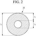
- FIG. 2 is a schematic cross-sectional view of porous silica according to some exemplary embodiments.
- the display device includes a display panel 100 and a window 300 disposed on the display panel 100.
- An adhesive layer 220 adhering the display panel 100 and the window 300 is disposed between the display panel 100 and the window 300.
- the display panel 100 may be flexible, stretchable, foldable, bendable, rollable, and/or otherwise deformable.
- flexible, stretchable, foldable, bendable, rollable, and/or otherwise deformable will be individually and/or collectively referred to as flexible.
- the display panel 100 may have flexibility such that it can be bent, but the display panel 100 is not limited thereto.
- the display panel 100 may be flat or include at least one flat portion and at least one flexible portion without limitation.
- the display panel 100 may be an organic light-emitting display (OLED) panel. Although not shown, the display panel 100 may at least include a substrate, a plurality of thin film transistors disposed on the substrate, and a plurality of electrodes.
- OLED organic light-emitting display
- the display panel 100 may be at least one of a liquid crystal display panel (LCD), a quantum dot organic light-emitting display panel (QD-OLED), an inorganic light-emitting display panel, a quantum dot liquid crystal display panel (QD-LCD), a quantum nano-emitting display panel (QNED), a micro light-emitting display panel, an electrophoretic display panel, an electrowetting display panel, and the like.
- LCD liquid crystal display panel
- QD-OLED quantum dot organic light-emitting display panel
- QD-LCD quantum dot liquid crystal display panel
- QNED quantum nano-emitting display panel
- micro light-emitting display panel an electrophoretic display panel
- electrowetting display panel and the like.
- the adhesive layer 220 is positioned between the display panel 100 and the window 300.
- the adhesive layer 220 combines (or otherwise couples) the display panel 100 and the window 300.
- the adhesive layer 220 may be a transparent polymer resin layer, and for example, may include at least one of an optically clear adhesive (OCA), an optically clear resin (OCR), a pressure sensitive adhesive (PSA), and a super view resin (SVR), but exemplary embodiments are not limited thereto.
- OCA optically clear adhesive
- OCR optically clear resin
- PSA pressure sensitive adhesive
- SVR super view resin
- a light blocking layer 210 may be disposed between the adhesive layer 220 and the window 300.
- the light blocking layer 210 may include a material capable of blocking and/or absorbing light.
- the light blocking layer 210 may be disposed to correspond to a bezel region of the display device according to some exemplary embodiments. According to some exemplary embodiments, the light blocking layer 210 may be omitted.
- the window 300 is disposed on the display panel 100, and may be attached to the display panel 100 by the adhesive layer 220.
- the window 300 may protect the display panel 100 from the outside, e.g., protect the display panel 100 from dust, debris, moisture, impact, etc.
- the window 300 includes a base layer 310 and a first coating layer 330.
- the base layer 310 may have a plate shape.
- the base layer 310 may be a glass substrate or a plastic substrate according to some exemplary embodiments.
- the configuration of the base layer 310 is composed of a single layer, but the base layer 310 may be formed of a plurality of layers.
- the base layer 310 may include, for example, a glass material including a silicate.
- the glass material may further contain (or include) an additional material to provide durability, surface smoothness, and transparency.
- base layer 310 may include at least of one aluminosilicates, borosilicates, boro-aluminosilicates, and the like.
- the base layer 310 may further include at least one of an alkali metal, an alkaline earth metal, and an oxide thereof. It is contemplated, however, that exemplary embodiments are not limited to the aforementioned materials for the base layer 310.
- the base layer 310 may include a first surface 311 facing the first coating layer 330, and a second surface 312 facing the display panel 100. Also, the base layer 310 includes a vertical surface 315 that is perpendicular to the first surface 311 and the second surface 312.
- the first coating layer 330 is disposed on the outer surface of the window 300.
- the first coating layer 330 may overlap the first surface 311 of the base layer 310.
- the first coating layer 330 may be in direct contact with the first surface 311 of the base layer 310, but exemplary embodiments are not limited thereto.
- the first coating layer 330 may be disposed on the first surface 311 on which a user's touch is directly performed.
- the first coating layer 330 may have at least one of an anti-glare, anti-reflective, and anti-fingerprint characteristic or function for preventing (or reducing) at least fingerprints from appearing on the window 300.
- the first coating layer 330 may be a single layer.
- the first coating layer 330 may provide the effects of the anti-glare, the anti-reflective, and/or the anti-fingerprint characteristics through one layer.
- the first coating layer 330 may include at least two of a siloxane-based compound containing fluorine, porous silica, and fumed silica.
- the first coating layer 330 may include a siloxane-based compound containing fluorine and porous silica, a siloxane-based compound containing fluorine and fumed silica, porous silica and fumed silica, and/or a siloxane-based compound containing fluorine, porous silica, and fumed silica.
- the first coating layer 330 may include a cured body of a first solution (or compound).
- the first solution may include at least two among the siloxane-based compound containing fluorine, porous silica, and fumed silica.
- the first solution may include the siloxane-based compound containing fluorine and porous silica, the siloxane-based compound containing fluorine and fumed silica, porous silica and fumed silica, or the siloxane-based compound containing fluorine, porous silica, and fumed silica.
- the siloxane-based compound containing fluorine may include, for example, heptadecafluorodecyltrimethoxysilane, tridecafluorooctyltriethoxysilane, or heptadecafluorodecyl triisopropoxysilane.
- the siloxane-based compound containing fluorine may be included in an amount ranging from about 4 weight percent (wt%) to about 7 wt% for the entire content in the first solution.
- the siloxane-based compound containing fluorine may be included in an amount of about 5 wt% to about 6 wt%, e.g., about 4 wt% to about 5 wt%, for instance about 6 wt% to about 7 wt%, for example, about 4.5 wt% to about 6.5 wt%.
- the first coating layer 330 containing the siloxane-based compound containing fluorine may provide the anti-fingerprint effect to the window 300.
- a contact angle for the first coating layer 330 may increase by the siloxane-based compound containing fluorine.
- the porous silica may include, for example, silicon dioxide.
- the porous silica may be included within the range of about 4 wt% to about 7 wt% for the entire content of the first solution. If the content of the porous silica is out of the above-described content, it may be difficult to simultaneously achieve the anti-glare, anti-reflection, and anti-fingerprint effects of the window 300. Also, The porous silica may be included within the range of about 5 wt% to about 6 wt%, e.g., about 4 wt% to about 5 wt%, for instance about 6 wt% to about 7 wt%, for example, about 4.5 wt% to about 6.5 wt%.
- the porous silica 33 may include hollows.
- the porous silica 33 has a shape having empty spaces formed therein.
- the porous silica 33 may be formed in an annular configuration, but exemplary embodiments are not limited thereto.
- the diameter t1 of the porous silica 33 may be from about 50 nm to about 100 nm, e.g., about 70 nm to about 80 nm, such as about 50 nm to about 70 nm, for instance, about 75 nm to about 100 nm, for example, about 60 nm to about 75 nm.
- the diameter t3 of the hollow included in the porous silica 33 may be from about 30 nm to about 60 nm, such as about 40 nm to about 50 nm, e.g., about 30 nm to about 45 nm, for instance, about 45 nm to about 60 nm, for example, about 45 nm to about 55 nm.
- the thickness t2 of the shell surrounding the hollow may be from about 10 nm to about 30 nm, such as about 15 nm to about 25 nm, e.g., about 20 nm to about 30 nm, for instance, about 10 nm to about 25 nm, for example, about 20 nm to about 25 nm.
- the first coating layer 330 containing porous silica may have the effect (or function) of preventing the reflection by (or form) external light.
- the surface reflectance of the first coating layer 330 including the porous silica may be greater than 0 and less than about 2.5 % and may be greater than 0 and less than about 1.3 % according to exemplary embodiments.
- the fumed silica may include, for example, amorphous fumed silica.
- the fumed silica may be included in an amount from about 0.1 wt% to about 0.5 wt% for the entire content of the first solution, e.g., about 0.2 wt% to about 0.4 wt%, such as about 0.1 wt% to about 0.3 wt%, for instance, about 0.3 wt% to about 0.5 wt%, for example, about 0.25 wt% to about 0.35 wt%. If the content of the fumed silica is out of the above-described content, it may be difficult to simultaneously achieve the anti-glare, anti-reflection, and anti-fingerprint effects of the window 300.
- the diameter of the fumed silica may be from about 5 nm to about 10 nm, e.g., about 6 nm to about 9 nm, such as about 5 nm to about 8 nm, for instance, about 7 nm to about 10 nm, for example, about 7 nm to about 8 nm.
- the first coating layer 330 containing the fumed silica may have the effect of preventing glare.
- the gloss of the window 300, including the first coating layer 330 including the fumed silica may be from about 100 gloss units (GU) to about 120 GU, e.g., 105 GU to about 115 GU, such as 110 GU to about 120 GU, for instance, 100 GU to about 115 GU, for example, 108 GU to about 112 GU.
- GU gloss units
- the first solution may contain at least one of an epoxy silane, an acid catalyst, and a solvent.
- the epoxy silane may include, for example, a trimethoxy silane.
- the epoxy silane may be included in an amount ranging from about 3 wt% to about 5 wt% for the entire content of the first solution, e.g., about 3.5 wt% to about 4.5 wt%, such as about 3 wt% to about 4 wt%., for instance, about 4 wt% to about 5 wt%, for example, about 3.8 wt% to about 4.2 wt%.
- the acid catalyst may include benzene tetracarboxylic anhydride.
- the acid catalyst may be included in an amount from about 0.1 wt% to about 0.5 wt% for the entire content of the first solution, e.g., about 0.2 wt% to about 0.4 wt%, such as about 0.1 wt% to about 0.3 wt%, for instance, about 0.3 wt% to about 0.5 wt%, for example, about 0.25 wt% to about 0.35 wt%.
- the first solution may contain a residual solvent, and the residual solvent may be, for example, propylene glycol methyl ether.
- the viscosity of the first solution may be from about 1.0 centipoise (cps) to about 5.0 cps, e.g., about 2.0 cps to about 4.0 cps, such as about 1.0 cps to about 3.5 cps, for instance, about 3 cps to about 5.0 cps, for example, about 2.5 cps to about 3.5 cps.
- cps centipoise
- the first coating layer 330 may be formed on the base layer 310 by using a wet coating method.
- the first coating layer 330 may be formed using a slip coater, a bar coater, a spin coater, a spray coater, and/or the like, for example.
- the first solution may be coated on the base layer 310 using the spray coater, and the coated solution may be cured at 180°C to 200°C for 30 minutes to form the first coating layer 330.
- a deposition distance deviation may occur depending on a height deviation of the base layer 310 provided during the manufacturing process. As such, a dry coating method formed first coating layer may not be formed uniformly and a color distortion due to the dry coating formed first coating layer may occur.
- the first coating layer 330 when the first coating layer 330 is formed using the wet coating method, according to some exemplary embodiments, the first coating layer 330 may be uniformly formed on the base layer 310. Since the color distortion caused by the window 300 may be reduced, an excellent (or at least improved) quality display device may be provided.
- the first coating layer 330 may include the fumed silica, the porous silica, and the siloxane-based compound containing fluorine, which are contained in one layer.
- the first coating layer 330 according to some exemplary embodiments can have a variety of effects through the single layer, which may provide the window 300 with a simple manufacturing process and excellent quality.
- FIG. 3 is a schematic cross-sectional view of a display device according to some exemplary embodiments. The description of the same configurations as the above-described configurations is omitted.
- the display device may include a housing 400 surrounding the display panel 100 and the window 300_1.
- the housing 400 is not limited to the illustrated form, and may have any form surrounding the display panel 100 and the window 300.
- the window 300_1 includes the base layer 310_1 and the first coating layer 330_1.
- the base layer 310_1 may be a glass substrate or a plastic substrate.
- the base layer 310_1 may include, for example, a glass material including a silicate.
- the glass material may further contain an additional material to provide durability, surface smoothness, and transparency.
- the base layer 310_1 may include at least one of aluminosilicates, borosilicates, boro-aluminosilicates, and the like.
- the base layer 310_1 may further include at least one of an alkali metal, an alkali earth metal, and an oxide thereof, but exemplary embodiments are not limited to the above-mentioned materials.
- the base layer 310_1 includes the first surface 311 facing the first coating layer 330, the second surface 312 facing the display panel 100, and the vertical surface 315 perpendicular to the first surface 311 and the second surface 312.
- the first surface 311 is a surface facing the user (or first coating layer 330_1)
- the second surface 312 is a surface facing the display panel 100 and overlapping the light blocking layer 210 and the adhesive layer 220.
- the base layer 310_1 may include a first inclination surface 313 that is inclined with respect to the first surface 311, e.g., inclined at an angle greater than 0° and less than 90°.
- the first inclination surface 313 connects the first surface 311 and the vertical surface 315.
- the base layer 310_1 may include a second inclination surface 314 that is inclined with respect to the second surface 312, e.g., inclined at an angle greater than 0° and less than 90°.
- the second inclination surface 314 connects the second surface 312 and the vertical surface 315.
- the first coating layer 330_1 may overlap the first surface 311 of the base layer 310. Also, the first coating layer 330_1 may overlap with a portion of the first inclination surface 313, but exemplary embodiments are not limited thereto.
- the first coating layer 330_1 may have an inclined shape along one side of the base layer 310_1, for example, along the first inclination surface 313 of the base layer 310_1.
- the first coating layer 330_1 may be formed of a solution having a predetermined viscosity. In the process of coating and curing the solution, the end of the first coating layer 330_1 may have a tapered shape toward one side of the base layer 310_1. The thickness of the end of the first coating layer 330_1 may be reduced toward the first inclination surface 313 of the base layer 310.
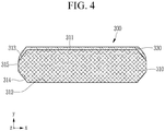
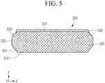
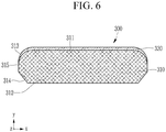
- FIGS. 4 , 5 , and 6 are cross-sectional views of a window according to various exemplary embodiments. The description of the same components as the above-described components is omitted.
- the end of the first coating layer 330_2 may have an inclined shape along the first inclination surface 313.
- the first coating layer 330_2 may be formed of the solution having a predetermined viscosity.
- the end of the first coating layer 330_2 may have a tapered shape toward one side of the base layer 310_1.
- the thickness of the end of the first coating layer 330_2 may be reduced toward the first inclination surface 313 of the base layer 310_1.
- the end of the first coating layer 330_2 may be aligned with the end of the first inclination surface 313.
- exemplary embodiments are not limited thereto.
- the first coating layer 330 2 may completely cover the first inclination surface 313 and the end thereof may be disposed on the vertical surface 315.
- the first inclination surface 313_1 connecting the first surface 311 and the vertical surface 315 of the base layer 310_2 may include a curved surface of a convex shape.
- the first inclination surface 313_1 having the curved surface of the convex shape has been described, exemplary embodiments are not limited thereto.
- the shape of the first inclination surface 313_1 may include any shape having the curved surface of a concave shape or having a curvature.
- the first coating layer 330_1 may partially overlap the first inclination surface 313_1 of the convex shape.
- the end of the first coating layer 330_1 may overlap the first inclination surface 313 of the convex shape.
- the first inclination surface 313_1 connecting the first surface 311 of the base layer 310_2 and the vertical surface 315 may include the curved surface of the convex shape.
- the end of the first coating layer 330_3 may have the inclined shape along the first inclination surface 313_1.
- the first coating layer 330_3 may be formed of the solution having the predetermined viscosity. In the process of coating and curing the solution, the end of the first coating layer 330_3 may have the tapered shape toward one side of the base layer 310_2. The thickness of the end of the first coating layer 330_3 may be reduced toward the first inclination surface 313 of the base layer 310_2.
- the first coating layer 330 3 may overlap the first inclination surface 313_1 of the convex shape.
- the first coating layer 330_3 may completely cover the first inclination surface 313_1 of the convex shape according to some exemplary embodiments.
- the end of the first coating layer 330_3 may be aligned with the end of the first inclination surface 313_1, but exemplary embodiments are not limited thereto.
- the end of the first coating layer 330_3 may be disposed on the vertical surface 315.
- FIG. 7 is a graph showing reflectance of a comparative example and according to some exemplary embodiments.
- FIG. 8 is an image showing color coordinates of a comparative example and according to some exemplary embodiments.
- the exemplary embodiment is a window including a base layer and a first coating layer consisting of one layer
- Comparative Example 1 to Comparative Example 4 show windows separately including a base layer, a surface-treatment layer for the anti-glare, an anti-reflective coating layer, and an anti-fingerprint coating layer.
- Comparative Example 1 to Comparative Example 4 include the same surface-treatment layer and coating layer, but the thickness or performance of the base layer is different.
- the exemplary embodiment exhibits almost constant reflectance (about 1.3 % to about 1.7 %) in the entire wavelength region of about 400 nm to about 700 nm.
- the window according to the exemplary embodiment exhibits uniform reflectance over the entire wavelength region such that there is no distortion of the provided color and the reflection reduction effect of the external light may be excellent.
- the exemplary embodiment has closer color coordinates to a color coordinate center. In other words, it is confirmed that the color purity of the exemplary embodiment is superior to that of the comparative examples.
- the color coordinates (a*, b*) according to the exemplary embodiment may be 0.45 and 0.11, and thus, the appearance of the window represents a neutral color.
- the color coordinates may be -1.55 and -1.55, and as shown in FIG. 8 , the appearance represents a light blue color.
- the color coordinates of the Comparative Example 5 may be -0.07 and -2.06, and it may be confirmed that the appearance represents a light purple color.
- Comparative Example 5 includes the same surface-treatment layer and coating layer as that of the above-described Comparative Example 1 to Comparative Example 4, but the base layer of the window is different. It is noted that Comparative Example 5 is not illustrated in FIG. 8 , but provided in Table 1. Table 1 Gloss Surface Reflection (%) Appearance Contact Angle Surface Hardness (GU) (Degrees) Exemplary Embodiment 104.8 1.31 Neutral 120.6 5H Comparative Example 2 94.5 0.51 Light Blue 119.0 5-6H Comparative Example 5 101.2 0.71 Light Purple 114.5 5-6H
- the gloss according to the exemplary embodiment is about 104.8 GU
- the gloss according to Comparative Example 2 is about 94.5 GU
- the gloss according to Comparative Example 5 is about 101.2 GU. It may be confirmed that even if only one layer is included according to the exemplary embodiment, sufficient gloss is obtained.
- the surface reflection, the contact angle, and the surface hardness in the exemplary embodiment are similar to those in the comparative example. Compared with the comparative example separately including the anti-reflection layer, the anti-fingerprint layer, and the like, it is confirmed that the exemplary embodiment including only one layer also has the sufficient reflection preventing effect, surface hardness, and fingerprint preventing effect (the contact angle).
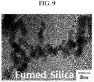
- FIG. 9 is an image of fumed silica according to some exemplary embodiments.
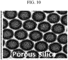
- FIG. 10 is an image of porous silica according to some exemplary embodiments.
- the fumed silica according to some exemplary embodiments has the diameter of about 5 nm to about 10 nm. Also, referring to FIG. 10 , it may be confirmed that the porous silica according to some exemplary embodiments has a spherical shape including the hollow.
- a manufacturing cost may be about one sixth of that of at least one of the comparative examples such that it may be excellent in terms of a manufacturing cost reduction.
Landscapes
- Chemical & Material Sciences (AREA)
- Engineering & Computer Science (AREA)
- Physics & Mathematics (AREA)
- Organic Chemistry (AREA)
- General Physics & Mathematics (AREA)
- Life Sciences & Earth Sciences (AREA)
- Materials Engineering (AREA)
- Theoretical Computer Science (AREA)
- Computer Hardware Design (AREA)
- Optics & Photonics (AREA)
- Wood Science & Technology (AREA)
- Chemical Kinetics & Catalysis (AREA)
- Nonlinear Science (AREA)
- General Engineering & Computer Science (AREA)
- Human Computer Interaction (AREA)
- Inorganic Chemistry (AREA)
- General Chemical & Material Sciences (AREA)
- Geochemistry & Mineralogy (AREA)
- Mathematical Physics (AREA)
- Crystallography & Structural Chemistry (AREA)
- Polymers & Plastics (AREA)
- Composite Materials (AREA)
- Medicinal Chemistry (AREA)
- Health & Medical Sciences (AREA)
- Dispersion Chemistry (AREA)
- Nanotechnology (AREA)
- Microelectronics & Electronic Packaging (AREA)
- Devices For Indicating Variable Information By Combining Individual Elements (AREA)
- Liquid Crystal (AREA)
- Surface Treatment Of Optical Elements (AREA)
- Laminated Bodies (AREA)
Abstract
Description
- Exemplary embodiments generally relate to a window, a method of manufacturing a window, and a display device including a window.
- A variety of mobile electronic devices may use a display device including a liquid crystal display (LCD), an organic light-emitting diode (OLED) display, or the like, such as mobile phones, navigation systems, digital cameras, electronic books, portable game machines, various terminals, etc. A typical display device used in such mobile electronic devices may have a transparent cover window (hereinafter, a window), which is provided at the front of a display panel and through which a user can see an image. Since the window may be formed at the outermost position of the device, the window should be resistant to an external environment so as to protect the display panel of (e.g., inside) the display device. Further, instead of a conventional method in which a switch or keyboard is used as an input device, a structure employing a touch panel having a display screen integrated therewith are being implemented. As such, the surface of the window may be more frequently contacted with a finger or the like than mobile devices utilizing conventional input mechanisms.
- The above information disclosed in this section is only for understanding the background of the inventive concepts, and, therefore, may contain information that does not form prior art.
- Some exemplary embodiments are capable of providing a window having a simple manufacturing process and a thin thickness.
- Some exemplary embodiments are capable of providing a method of manufacturing a window with a thin thickness and a simple manufacturing process.
- Some exemplary embodiments are capable of providing a display device including a window having a simple manufacturing process and a thin thickness.
- Additional aspects will be set forth in the detailed description which follows, and, in part, will be apparent from the disclosure, or may be learned by practice of the inventive concepts.
- According to some exemplary embodiments, a window includes a base layer and a first coating layer. The first coating layer is disposed on a first surface of the base layer. The first coating layer is a single layer. The first coating layer includes a siloxane-based compound. The siloxane-based compound includes fluorine and silica.
- According to some exemplary embodiments, a display device includes a display panel and a window. The window includes a base layer and a first coating layer. The first coating layer is disposed on the base layer. The first coating layer is a single layer. The first coating layer includes porous silica and fumed silica.
- According to some exemplary embodiments, a method of manufacturing a window includes preparing a base layer of the window; and forming, via a wet coating process, a first coating layer on a first surface of the base layer. The first coating layer is formed of a single layer. The first coating layer includes at least two of porous silica, fumed silica, and a siloxane-based compound. The siloxane-based compound includes fluorine.
- According to various exemplary embodiments, a process of manufacturing a window is simplified, and, as such, not only may manufacturing time be reduced, but so too may manufacturing costs. In addition, anti-reflection, anti-glare, and anti-fingerprint functions may be provided by the window, e.g., a surface of the window.
- The foregoing general description and the following detailed description are exemplary and explanatory and are intended to provide further explanation of the claimed subject matter.
- The accompanying drawings, which are included to provide a further understanding of the inventive concepts, and are incorporated in and constitute a part of this specification, illustrate exemplary embodiments of the inventive concepts, and, together with the description, serve to explain principles of the inventive concepts.
-
FIG. 1 is a schematic cross-sectional view of a display device according to some exemplary embodiments. -
FIG. 2 is a schematic cross-sectional view of porous silica according to some exemplary embodiments. -
FIG. 3 is a schematic cross-sectional view of a display device according to some exemplary embodiments. -
FIGS. 4 ,5 , and6 are cross-sectional views of a window according to various exemplary embodiments. -
FIG. 7 is a graph showing reflectance of a comparative example and according to some exemplary embodiments. -
FIG. 8 is an image showing color coordinates of a comparative example and according to some exemplary embodiments. -
FIG. 9 is an image of fumed silica according to some exemplary embodiments. -
FIG. 10 is an image of porous silica according to some exemplary embodiments. - In the following description, for the purposes of explanation, numerous specific details are set forth in order to provide a thorough understanding of various exemplary embodiments. As used herein, the terms "embodiments" and "implementations" are used interchangeably and are non-limiting examples employing one or more of the inventive concepts disclosed herein. It is apparent, however, that various exemplary embodiments may be practiced without these specific details or with one or more equivalent arrangements. In other instances, well-known structures and devices are shown in block diagram form in order to avoid unnecessarily obscuring various exemplary embodiments. Further, various exemplary embodiments may be different, but do not have to be exclusive. For example, specific shapes, configurations, and characteristics of an exemplary embodiment may be used or implemented in another exemplary embodiment without departing from the inventive concepts.
- Unless otherwise specified, the illustrated exemplary embodiments are to be understood as providing exemplary features of varying detail of some exemplary embodiments. Therefore, unless otherwise specified, the features, components, modules, layers, films, panels, regions, aspects, etc. (hereinafter individually or collectively referred to as an "element" or "elements"), of the various illustrations may be otherwise combined, separated, interchanged, and/or rearranged without departing from the inventive concepts.
- The use of cross-hatching and/or shading in the accompanying drawings is generally provided to clarify boundaries between adjacent elements. As such, neither the presence nor the absence of cross-hatching or shading conveys or indicates any preference or requirement for particular materials, material properties, dimensions, proportions, commonalities between illustrated elements, and/or any other characteristic, attribute, property, etc., of the elements, unless specified. Further, in the accompanying drawings, the size and relative sizes of elements may be exaggerated for clarity and/or descriptive purposes. As such, the sizes and relative sizes of the respective elements are not necessarily limited to the sizes and relative sizes shown in the drawings. When an exemplary embodiment may be implemented differently, a specific process order may be performed differently from the described order. For example, two consecutively described processes may be performed substantially at the same time or performed in an order opposite to the described order. Also, like reference numerals denote like elements.
- When an element, such as a layer, is referred to as being "on," "connected to," or "coupled to" another element, it may be directly on, connected to, or coupled to the other element or intervening elements may be present. When, however, an element is referred to as being "directly on," "directly connected to," or "directly coupled to" another element, there are no intervening elements present. Other terms and/or phrases used to describe a relationship between elements should be interpreted in a like fashion, e.g., "between" versus "directly between," "adjacent" versus "directly adjacent," "on" versus "directly on," etc. Further, the term "connected" may refer to physical, electrical, and/or fluid connection. In addition, the X-axis, the Y-axis, and the Z-axis are not limited to three axes of a rectangular coordinate system, and may be interpreted in a broader sense. For example, the X-axis, the Y-axis, and the Z-axis may be perpendicular to one another, or may represent different directions that are not perpendicular to one another. For the purposes of this disclosure, "at least one of X, Y, and Z" and "at least one selected from the group consisting of X, Y, and Z" may be construed as X only, Y only, Z only, or any combination of two or more of X, Y, and Z, such as, for instance, XYZ, XYY, YZ, and ZZ. As used herein, the term "and/or" includes any and all combinations of one or more of the associated listed items.
- Although the terms "first," "second," etc. may be used herein to describe various elements, these elements should not be limited by these terms. These terms are used to distinguish one element from another element. Thus, a first element discussed below could be termed a second element without departing from the teachings of the disclosure.
- Spatially relative terms, such as "beneath," "below," "under," "lower," "above," "upper," "over," "higher," "side" (e.g., as in "sidewall"), and the like, may be used herein for descriptive purposes, and, thereby, to describe one element's relationship to another element(s) as illustrated in the drawings. Spatially relative terms are intended to encompass different orientations of an apparatus in use, operation, and/or manufacture in addition to the orientation depicted in the drawings. For example, if the apparatus in the drawings is turned over, elements described as "below" or "beneath" other elements or features would then be oriented "above" the other elements or features. Thus, the exemplary term "below" can encompass both an orientation of above and below. Furthermore, the apparatus may be otherwise oriented (e.g., rotated 90 degrees or at other orientations), and, as such, the spatially relative descriptors used herein interpreted accordingly. Further, for the purposes of this disclosure, the phrase "on a plane" means viewing the object portion from the top, and the phrase "on (or in) a cross-section" means viewing a cross-section of which the object portion is vertically cut from a side.
- The terminology used herein is for the purpose of describing particular embodiments and is not intended to be limiting. As used herein, the singular forms, "a," "an," and "the" are intended to include the plural forms as well, unless the context clearly indicates otherwise. Moreover, the terms "comprises," "comprising," "includes," and/or "including," when used in this specification, specify the presence of stated features, integers, steps, operations, elements, components, and/or groups thereof, but do not preclude the presence or addition of one or more other features, integers, steps, operations, elements, components, and/or groups thereof. It is also noted that, as used herein, the terms "substantially," "about," and other similar terms, are used as terms of approximation and not as terms of degree, and, as such, are utilized to account for inherent deviations in measured, calculated, and/or provided values that would be recognized by one of ordinary skill in the art.
- Various exemplary embodiments are described herein with reference to sectional views, isometric views, perspective views, plan views, and/or exploded illustrations that are schematic illustrations of idealized exemplary embodiments and/or intermediate structures. As such, variations from the shapes of the illustrations as a result of, for example, manufacturing techniques and/or tolerances, are to be expected. Thus, exemplary embodiments disclosed herein should not be construed as limited to the particular illustrated shapes of regions, but are to include deviations in shapes that result from, for instance, manufacturing. To this end, regions illustrated in the drawings may be schematic in nature and shapes of these regions may not reflect the actual shapes of regions of a device, and, as such, are not intended to be limiting.
- Unless otherwise defined, all terms (including technical and scientific terms) used herein have the same meaning as commonly understood by one of ordinary skill in the art to which this disclosure is a part. Terms, such as those defined in commonly used dictionaries, should be interpreted as having a meaning that is consistent with their meaning in the context of the relevant art and will not be interpreted in an idealized or overly formal sense, unless expressly so defined herein.
- As customary in the field, some exemplary embodiments are described and illustrated in the accompanying drawings in terms of functional blocks, units, and/or modules. Those skilled in the art will appreciate that these blocks, units, and/or modules are physically implemented by electronic (or optical) circuits, such as logic circuits, discrete components, microprocessors, hard-wired circuits, memory elements, wiring connections, and the like, which may be formed using semiconductor-based fabrication techniques or other manufacturing technologies. In the case of the blocks, units, and/or modules being implemented by microprocessors or other similar hardware, they may be programmed and controlled using software (e.g., microcode) to perform various functions discussed herein and may optionally be driven by firmware and/or software. It is also contemplated that each block, unit, and/or module may be implemented by dedicated hardware, or as a combination of dedicated hardware to perform some functions and a processor (e.g., one or more programmed microprocessors and associated circuitry) to perform other functions. Also, each block, unit, and/or module of some exemplary embodiments may be physically separated into two or more interacting and discrete blocks, units, and/or modules without departing from the inventive concepts. Further, the blocks, units, and/or modules of some exemplary embodiments may be physically combined into more complex blocks, units, and/or modules without departing from the inventive concepts.
- Hereinafter, various exemplary embodiments will be explained in detail with reference to the accompanying drawings.
- Now, a display device according to some exemplary embodiments is described with reference to
FIGS. 1 and2 .FIG. 1 is a schematic cross-sectional view of a display device according to some exemplary embodiments.FIG. 2 is a schematic cross-sectional view of porous silica according to some exemplary embodiments. - As shown in
FIG. 1 , the display device according to some exemplary embodiments includes adisplay panel 100 and awindow 300 disposed on thedisplay panel 100. Anadhesive layer 220 adhering thedisplay panel 100 and thewindow 300 is disposed between thedisplay panel 100 and thewindow 300. - The
display panel 100 may be flexible, stretchable, foldable, bendable, rollable, and/or otherwise deformable. Hereinafter, the terms flexible, stretchable, foldable, bendable, rollable, and/or otherwise deformable will be individually and/or collectively referred to as flexible. Thedisplay panel 100 may have flexibility such that it can be bent, but thedisplay panel 100 is not limited thereto. For instance, thedisplay panel 100 may be flat or include at least one flat portion and at least one flexible portion without limitation. - The
display panel 100 may be an organic light-emitting display (OLED) panel. Although not shown, thedisplay panel 100 may at least include a substrate, a plurality of thin film transistors disposed on the substrate, and a plurality of electrodes. - Although the
display panel 100 has been described as being an OLED panel, exemplary embodiments are not limited thereto. According to some exemplary embodiments, thedisplay panel 100 may be at least one of a liquid crystal display panel (LCD), a quantum dot organic light-emitting display panel (QD-OLED), an inorganic light-emitting display panel, a quantum dot liquid crystal display panel (QD-LCD), a quantum nano-emitting display panel (QNED), a micro light-emitting display panel, an electrophoretic display panel, an electrowetting display panel, and the like. - The
adhesive layer 220 is positioned between thedisplay panel 100 and thewindow 300. Theadhesive layer 220 combines (or otherwise couples) thedisplay panel 100 and thewindow 300. Theadhesive layer 220 may be a transparent polymer resin layer, and for example, may include at least one of an optically clear adhesive (OCA), an optically clear resin (OCR), a pressure sensitive adhesive (PSA), and a super view resin (SVR), but exemplary embodiments are not limited thereto. - A
light blocking layer 210 may be disposed between theadhesive layer 220 and thewindow 300. Thelight blocking layer 210 may include a material capable of blocking and/or absorbing light. Thelight blocking layer 210 may be disposed to correspond to a bezel region of the display device according to some exemplary embodiments. According to some exemplary embodiments, thelight blocking layer 210 may be omitted. - The
window 300 is disposed on thedisplay panel 100, and may be attached to thedisplay panel 100 by theadhesive layer 220. Thewindow 300 may protect thedisplay panel 100 from the outside, e.g., protect thedisplay panel 100 from dust, debris, moisture, impact, etc. - The
window 300 according to some exemplary embodiments includes abase layer 310 and afirst coating layer 330. - The
base layer 310 may have a plate shape. Thebase layer 310 may be a glass substrate or a plastic substrate according to some exemplary embodiments. For descriptive and illustrative convenience, the configuration of thebase layer 310 is composed of a single layer, but thebase layer 310 may be formed of a plurality of layers. - The
base layer 310 may include, for example, a glass material including a silicate. The glass material may further contain (or include) an additional material to provide durability, surface smoothness, and transparency. For example,base layer 310 may include at least of one aluminosilicates, borosilicates, boro-aluminosilicates, and the like. Thebase layer 310 may further include at least one of an alkali metal, an alkaline earth metal, and an oxide thereof. It is contemplated, however, that exemplary embodiments are not limited to the aforementioned materials for thebase layer 310. - The
base layer 310 may include afirst surface 311 facing thefirst coating layer 330, and asecond surface 312 facing thedisplay panel 100. Also, thebase layer 310 includes avertical surface 315 that is perpendicular to thefirst surface 311 and thesecond surface 312. - The
first coating layer 330 is disposed on the outer surface of thewindow 300. Thefirst coating layer 330 may overlap thefirst surface 311 of thebase layer 310. Thefirst coating layer 330 may be in direct contact with thefirst surface 311 of thebase layer 310, but exemplary embodiments are not limited thereto. Thefirst coating layer 330 may be disposed on thefirst surface 311 on which a user's touch is directly performed. Thefirst coating layer 330 may have at least one of an anti-glare, anti-reflective, and anti-fingerprint characteristic or function for preventing (or reducing) at least fingerprints from appearing on thewindow 300. - The
first coating layer 330 may be a single layer. Thefirst coating layer 330 may provide the effects of the anti-glare, the anti-reflective, and/or the anti-fingerprint characteristics through one layer. - The
first coating layer 330 may include at least two of a siloxane-based compound containing fluorine, porous silica, and fumed silica. Thefirst coating layer 330 may include a siloxane-based compound containing fluorine and porous silica, a siloxane-based compound containing fluorine and fumed silica, porous silica and fumed silica, and/or a siloxane-based compound containing fluorine, porous silica, and fumed silica. - The
first coating layer 330 may include a cured body of a first solution (or compound). The first solution may include at least two among the siloxane-based compound containing fluorine, porous silica, and fumed silica. The first solution may include the siloxane-based compound containing fluorine and porous silica, the siloxane-based compound containing fluorine and fumed silica, porous silica and fumed silica, or the siloxane-based compound containing fluorine, porous silica, and fumed silica. - The siloxane-based compound containing fluorine may include, for example, heptadecafluorodecyltrimethoxysilane, tridecafluorooctyltriethoxysilane, or heptadecafluorodecyl triisopropoxysilane. The siloxane-based compound containing fluorine may be included in an amount ranging from about 4 weight percent (wt%) to about 7 wt% for the entire content in the first solution. When the content of the siloxane-based compound containing fluorine is out of the above-described content, it may be difficult to simultaneously achieve the anti-glare, anti-reflection, and anti-fingerprint effects of the
window 300. Also, The siloxane-based compound containing fluorine may be included in an amount of about 5 wt% to about 6 wt%, e.g., about 4 wt% to about 5 wt%, for instance about 6 wt% to about 7 wt%, for example, about 4.5 wt% to about 6.5 wt%. - According to some exemplary embodiments, the
first coating layer 330 containing the siloxane-based compound containing fluorine may provide the anti-fingerprint effect to thewindow 300. A contact angle for thefirst coating layer 330 may increase by the siloxane-based compound containing fluorine. - In some exemplary embodiments, the porous silica may include, for example, silicon dioxide. The porous silica may be included within the range of about 4 wt% to about 7 wt% for the entire content of the first solution. If the content of the porous silica is out of the above-described content, it may be difficult to simultaneously achieve the anti-glare, anti-reflection, and anti-fingerprint effects of the
window 300. Also, The porous silica may be included within the range of about 5 wt% to about 6 wt%, e.g., about 4 wt% to about 5 wt%, for instance about 6 wt% to about 7 wt%, for example, about 4.5 wt% to about 6.5 wt%. - The
porous silica 33, as shown inFIG. 2 , may include hollows. Theporous silica 33 has a shape having empty spaces formed therein. For instance, theporous silica 33 may be formed in an annular configuration, but exemplary embodiments are not limited thereto. - The diameter t1 of the
porous silica 33 may be from about 50 nm to about 100 nm, e.g., about 70 nm to about 80 nm, such as about 50 nm to about 70 nm, for instance, about 75 nm to about 100 nm, for example, about 60 nm to about 75 nm. The diameter t3 of the hollow included in theporous silica 33 may be from about 30 nm to about 60 nm, such as about 40 nm to about 50 nm, e.g., about 30 nm to about 45 nm, for instance, about 45 nm to about 60 nm, for example, about 45 nm to about 55 nm. The thickness t2 of the shell surrounding the hollow may be from about 10 nm to about 30 nm, such as about 15 nm to about 25 nm, e.g., about 20 nm to about 30 nm, for instance, about 10 nm to about 25 nm, for example, about 20 nm to about 25 nm. - According to some exemplary embodiments, the
first coating layer 330 containing porous silica may have the effect (or function) of preventing the reflection by (or form) external light. The surface reflectance of thefirst coating layer 330 including the porous silica may be greater than 0 and less than about 2.5 % and may be greater than 0 and less than about 1.3 % according to exemplary embodiments. - The fumed silica according to some exemplary embodiments may include, for example, amorphous fumed silica. The fumed silica may be included in an amount from about 0.1 wt% to about 0.5 wt% for the entire content of the first solution, e.g., about 0.2 wt% to about 0.4 wt%, such as about 0.1 wt% to about 0.3 wt%, for instance, about 0.3 wt% to about 0.5 wt%, for example, about 0.25 wt% to about 0.35 wt%. If the content of the fumed silica is out of the above-described content, it may be difficult to simultaneously achieve the anti-glare, anti-reflection, and anti-fingerprint effects of the
window 300. - The diameter of the fumed silica may be from about 5 nm to about 10 nm, e.g., about 6 nm to about 9 nm, such as about 5 nm to about 8 nm, for instance, about 7 nm to about 10 nm, for example, about 7 nm to about 8 nm.
- According to some exemplary embodiments, the
first coating layer 330 containing the fumed silica may have the effect of preventing glare. The gloss of thewindow 300, including thefirst coating layer 330 including the fumed silica, may be from about 100 gloss units (GU) to about 120 GU, e.g., 105 GU to about 115 GU, such as 110 GU to about 120 GU, for instance, 100 GU to about 115 GU, for example, 108 GU to about 112 GU. - Also, the first solution may contain at least one of an epoxy silane, an acid catalyst, and a solvent.
- The epoxy silane may include, for example, a trimethoxy silane. The epoxy silane may be included in an amount ranging from about 3 wt% to about 5 wt% for the entire content of the first solution, e.g., about 3.5 wt% to about 4.5 wt%, such as about 3 wt% to about 4 wt%., for instance, about 4 wt% to about 5 wt%, for example, about 3.8 wt% to about 4.2 wt%.
- The acid catalyst, for example, may include benzene tetracarboxylic anhydride. The acid catalyst may be included in an amount from about 0.1 wt% to about 0.5 wt% for the entire content of the first solution, e.g., about 0.2 wt% to about 0.4 wt%, such as about 0.1 wt% to about 0.3 wt%, for instance, about 0.3 wt% to about 0.5 wt%, for example, about 0.25 wt% to about 0.35 wt%.
- The first solution may contain a residual solvent, and the residual solvent may be, for example, propylene glycol methyl ether.
- The viscosity of the first solution may be from about 1.0 centipoise (cps) to about 5.0 cps, e.g., about 2.0 cps to about 4.0 cps, such as about 1.0 cps to about 3.5 cps, for instance, about 3 cps to about 5.0 cps, for example, about 2.5 cps to about 3.5 cps.
- The
first coating layer 330 may be formed on thebase layer 310 by using a wet coating method. Thefirst coating layer 330 may be formed using a slip coater, a bar coater, a spin coater, a spray coater, and/or the like, for example. For instance, the first solution may be coated on thebase layer 310 using the spray coater, and the coated solution may be cured at 180°C to 200°C for 30 minutes to form thefirst coating layer 330. If thefirst coating layer 330 is formed using a dry coating method, a deposition distance deviation may occur depending on a height deviation of thebase layer 310 provided during the manufacturing process. As such, a dry coating method formed first coating layer may not be formed uniformly and a color distortion due to the dry coating formed first coating layer may occur. - However, when the
first coating layer 330 is formed using the wet coating method, according to some exemplary embodiments, thefirst coating layer 330 may be uniformly formed on thebase layer 310. Since the color distortion caused by thewindow 300 may be reduced, an excellent (or at least improved) quality display device may be provided. - The
first coating layer 330 according to some exemplary embodiments may include the fumed silica, the porous silica, and the siloxane-based compound containing fluorine, which are contained in one layer. Thefirst coating layer 330 according to some exemplary embodiments can have a variety of effects through the single layer, which may provide thewindow 300 with a simple manufacturing process and excellent quality. - Next, a display device according to some exemplary embodiments is described with reference to
FIG. 3. FIG. 3 is a schematic cross-sectional view of a display device according to some exemplary embodiments. The description of the same configurations as the above-described configurations is omitted. - The display device according to some exemplary embodiments may include a
housing 400 surrounding thedisplay panel 100 and the window 300_1. Thehousing 400 is not limited to the illustrated form, and may have any form surrounding thedisplay panel 100 and thewindow 300. - The window 300_1 according to some exemplary embodiments includes the base layer 310_1 and the first coating layer 330_1.
- The base layer 310_1 may be a glass substrate or a plastic substrate. The base layer 310_1 may include, for example, a glass material including a silicate. The glass material may further contain an additional material to provide durability, surface smoothness, and transparency. For example, the base layer 310_1 may include at least one of aluminosilicates, borosilicates, boro-aluminosilicates, and the like. The base layer 310_1 may further include at least one of an alkali metal, an alkali earth metal, and an oxide thereof, but exemplary embodiments are not limited to the above-mentioned materials.
- According to some exemplary embodiments, the base layer 310_1 includes the
first surface 311 facing thefirst coating layer 330, thesecond surface 312 facing thedisplay panel 100, and thevertical surface 315 perpendicular to thefirst surface 311 and thesecond surface 312. Thefirst surface 311 is a surface facing the user (or first coating layer 330_1), and thesecond surface 312 is a surface facing thedisplay panel 100 and overlapping thelight blocking layer 210 and theadhesive layer 220. - The base layer 310_1 may include a
first inclination surface 313 that is inclined with respect to thefirst surface 311, e.g., inclined at an angle greater than 0° and less than 90°. Thefirst inclination surface 313 connects thefirst surface 311 and thevertical surface 315. The base layer 310_1 may include asecond inclination surface 314 that is inclined with respect to thesecond surface 312, e.g., inclined at an angle greater than 0° and less than 90°. Thesecond inclination surface 314 connects thesecond surface 312 and thevertical surface 315. - The first coating layer 330_1 may overlap the
first surface 311 of thebase layer 310. Also, the first coating layer 330_1 may overlap with a portion of thefirst inclination surface 313, but exemplary embodiments are not limited thereto. - The first coating layer 330_1 may have an inclined shape along one side of the base layer 310_1, for example, along the
first inclination surface 313 of the base layer 310_1. The first coating layer 330_1 may be formed of a solution having a predetermined viscosity. In the process of coating and curing the solution, the end of the first coating layer 330_1 may have a tapered shape toward one side of the base layer 310_1. The thickness of the end of the first coating layer 330_1 may be reduced toward thefirst inclination surface 313 of thebase layer 310. - Next, a display device according to some exemplary embodiments is described with reference to
FIGS. 4 to 6 .FIGS. 4 ,5 , and6 are cross-sectional views of a window according to various exemplary embodiments. The description of the same components as the above-described components is omitted. - First, referring to
FIG. 4 , the end of the first coating layer 330_2 may have an inclined shape along thefirst inclination surface 313. The first coating layer 330_2 may be formed of the solution having a predetermined viscosity. In the process of coating and curing the solution, the end of the first coating layer 330_2 may have a tapered shape toward one side of the base layer 310_1. The thickness of the end of the first coating layer 330_2 may be reduced toward thefirst inclination surface 313 of the base layer 310_1. - Also, the end of the first coating layer 330_2 may be aligned with the end of the
first inclination surface 313. However, exemplary embodiments are not limited thereto. For instance, thefirst coating layer 330 2 may completely cover thefirst inclination surface 313 and the end thereof may be disposed on thevertical surface 315. - Next, referring to
FIG. 5 , the first inclination surface 313_1 connecting thefirst surface 311 and thevertical surface 315 of the base layer 310_2 may include a curved surface of a convex shape. Although the first inclination surface 313_1 having the curved surface of the convex shape has been described, exemplary embodiments are not limited thereto. For instance, the shape of the first inclination surface 313_1 may include any shape having the curved surface of a concave shape or having a curvature. The first coating layer 330_1 may partially overlap the first inclination surface 313_1 of the convex shape. For example, the end of the first coating layer 330_1 may overlap thefirst inclination surface 313 of the convex shape. - Referring to
FIG. 6 , the first inclination surface 313_1 connecting thefirst surface 311 of the base layer 310_2 and thevertical surface 315 may include the curved surface of the convex shape. - The end of the first coating layer 330_3 may have the inclined shape along the first inclination surface 313_1. The first coating layer 330_3 may be formed of the solution having the predetermined viscosity. In the process of coating and curing the solution, the end of the first coating layer 330_3 may have the tapered shape toward one side of the base layer 310_2. The thickness of the end of the first coating layer 330_3 may be reduced toward the
first inclination surface 313 of the base layer 310_2. - The
first coating layer 330 3 may overlap the first inclination surface 313_1 of the convex shape. The first coating layer 330_3 may completely cover the first inclination surface 313_1 of the convex shape according to some exemplary embodiments. The end of the first coating layer 330_3 may be aligned with the end of the first inclination surface 313_1, but exemplary embodiments are not limited thereto. For instance, the end of the first coating layer 330_3 may be disposed on thevertical surface 315. - Next, an exemplary embodiment and a comparative example are described with reference to
FIGS. 7 and8 .FIG. 7 is a graph showing reflectance of a comparative example and according to some exemplary embodiments.FIG. 8 is an image showing color coordinates of a comparative example and according to some exemplary embodiments. - Referring to
FIG. 7 , the exemplary embodiment is a window including a base layer and a first coating layer consisting of one layer, and Comparative Example 1 to Comparative Example 4 show windows separately including a base layer, a surface-treatment layer for the anti-glare, an anti-reflective coating layer, and an anti-fingerprint coating layer. Comparative Example 1 to Comparative Example 4 include the same surface-treatment layer and coating layer, but the thickness or performance of the base layer is different. - As shown in
FIG. 7 , it may be confirmed that the exemplary embodiment exhibits almost constant reflectance (about 1.3 % to about 1.7 %) in the entire wavelength region of about 400 nm to about 700 nm. The window according to the exemplary embodiment exhibits uniform reflectance over the entire wavelength region such that there is no distortion of the provided color and the reflection reduction effect of the external light may be excellent. - On the other hand, in the case of Comparative Example 1 to Comparative Example 4, a reflectance difference of about 5 % is observed depending on the wavelength. In this case, some wavelengths may be excessively reflected compared to other wavelengths, and, as such, the distortion may occur in the color of the light provided to the user.
- Referring to
FIG. 8 , it may be confirmed that the exemplary embodiment has closer color coordinates to a color coordinate center. In other words, it is confirmed that the color purity of the exemplary embodiment is superior to that of the comparative examples. - For example, referring to
FIG. 8 and Table 1 below, the color coordinates (a*, b*) according to the exemplary embodiment may be 0.45 and 0.11, and thus, the appearance of the window represents a neutral color. On the other hand, in the case of Comparative Example 2, the color coordinates may be -1.55 and -1.55, and as shown inFIG. 8 , the appearance represents a light blue color. In case of Comparative Example 3, it may be confirmed that the appearance also represents the light blue color throughFIG. 8 . On the other hand, the color coordinates of the Comparative Example 5 may be -0.07 and -2.06, and it may be confirmed that the appearance represents a light purple color. Comparative Example 5 includes the same surface-treatment layer and coating layer as that of the above-described Comparative Example 1 to Comparative Example 4, but the base layer of the window is different. It is noted that Comparative Example 5 is not illustrated inFIG. 8 , but provided in Table 1.Table 1 Gloss Surface Reflection (%) Appearance Contact Angle Surface Hardness (GU) (Degrees) Exemplary Embodiment 104.8 1.31 Neutral 120.6 5H Comparative Example 2 94.5 0.51 Light Blue 119.0 5-6H Comparative Example 5 101.2 0.71 Light Purple 114.5 5-6H - Also, it is confirmed that the gloss according to the exemplary embodiment is about 104.8 GU, the gloss according to Comparative Example 2 is about 94.5 GU, and the gloss according to Comparative Example 5 is about 101.2 GU. It may be confirmed that even if only one layer is included according to the exemplary embodiment, sufficient gloss is obtained. In addition, it is confirmed that the surface reflection, the contact angle, and the surface hardness in the exemplary embodiment are similar to those in the comparative example. Compared with the comparative example separately including the anti-reflection layer, the anti-fingerprint layer, and the like, it is confirmed that the exemplary embodiment including only one layer also has the sufficient reflection preventing effect, surface hardness, and fingerprint preventing effect (the contact angle).
- Next, the material included in the first coating layer according to some exemplary embodiments is described with reference to
FIGS. 9 and10 .FIG. 9 is an image of fumed silica according to some exemplary embodiments.FIG. 10 is an image of porous silica according to some exemplary embodiments. - Referring to
FIG. 9 , it may be confirmed that the fumed silica according to some exemplary embodiments has the diameter of about 5 nm to about 10 nm. Also, referring toFIG. 10 , it may be confirmed that the porous silica according to some exemplary embodiments has a spherical shape including the hollow. - On the other hand, when the anti-glare treatment is separately performed like in at least one of the comparative examples, and the anti-reflection layer and the anti-fingerprint layer are separately included, the manufacturing cost for the manufacturing process may be considerably increased. According, however, to various exemplary embodiments, a manufacturing cost may be about one sixth of that of at least one of the comparative examples such that it may be excellent in terms of a manufacturing cost reduction.
- Although certain exemplary embodiments and implementations have been described herein, other embodiments and modifications will be apparent from this description.
Claims (15)
- A window (300) comprising:a base layer (310); anda first coating layer (330) disposed on a first surface (311) of the base layer (310),wherein:the first coating layer (330) is a single layer;the first coating layer (330) comprises a siloxane-based compound; andthe siloxane-based compound comprises fluorine and silica.
- The window (300) of claim 1, wherein the silica comprises porous silica and fumed silica.
- The window (300) of claim 2, wherein:the porous silica comprises a hollow; anda diameter of the hollow is from about 30 nm to about 60 nm.
- The window (300) of claim 3, wherein a thickness of a shell surrounding the hollow is from about 10 nm to about 30 nm.
- The window (300) of at least one of claims 2 to 4, wherein the fumed silica is amorphous fumed silica.
- The window (300) of at least one of claims 2 to 5, wherein a diameter of the fumed silica is from about 5 nm to about 10 nm.
- The window (300) of at least one of claims 1 to 6, wherein the siloxane-based compound containing fluorine includes heptadecafluorodecyltrimethoxysilane.
- The window (300) of at least one of claims 1 to 7, wherein an end portion of the first coating layer (330) is inclined along one surface of the base layer (310).
- The window (300) of at least one of claims 1 to 8, wherein the base layer (310) comprises:a second surface (312) overlapping the first surface (311);a vertical surface (315) perpendicular to the first surface (311) and the second surface (312);a first inclination surface (313) connecting the first surface (311) and the vertical surface (315); anda second inclination surface (314) connecting the second surface (312) and the vertical surface (315).
- The window (300) of claim 9, wherein the first coating layer (330) overlaps the first inclination surface (313).
- The window (300) of at least one of claims 9 or 10, wherein the first inclination surface (313) s a curved surface.
- A display device comprising:a display panel (100); anda window (300) overlapping the display panel (100),wherein the window (300) comprises:a base layer (310); anda first coating layer (330) disposed on the base layer (310),wherein:the first coating layer (330) is a single layer; andthe first coating layer (330) comprises porous silica and fumed silica.
- The display device of claim 12, wherein an end portion of the first coating layer (330) is inclined along one surface of the base layer (310).
- A method for manufacturing a window (300), comprising
preparing a base layer (310) of the window (300); and
forming, via a wet coating process, a first coating layer (330) on a first surface (311) of the base layer (310),
wherein:the first coating layer (330) is formed of a single layer;the first coating layer (330) comprises at least two of porous silica, fumed silica, and a siloxane-based compound; andthe siloxane-based compound comprises fluorine. - The method of claim 14, wherein the wet coating process is a spray process.
Applications Claiming Priority (1)
| Application Number | Priority Date | Filing Date | Title |
|---|---|---|---|
| KR1020190000284A KR102594548B1 (en) | 2019-01-02 | 2019-01-02 | Window, manufacturing method thereof and display device comprising the same |
Publications (2)
| Publication Number | Publication Date |
|---|---|
| EP3677985A1 true EP3677985A1 (en) | 2020-07-08 |
| EP3677985B1 EP3677985B1 (en) | 2023-05-10 |
Family
ID=68847982
Family Applications (1)
| Application Number | Title | Priority Date | Filing Date |
|---|---|---|---|
| EP19214710.6A Active EP3677985B1 (en) | 2019-01-02 | 2019-12-10 | Window, method of manufacturing window, and display device including window |
Country Status (6)
| Country | Link |
|---|---|
| US (1) | US11926759B2 (en) |
| EP (1) | EP3677985B1 (en) |
| JP (1) | JP7350251B2 (en) |
| KR (1) | KR102594548B1 (en) |
| CN (1) | CN111462613B (en) |
| TW (1) | TWI845588B (en) |
Families Citing this family (3)
| Publication number | Priority date | Publication date | Assignee | Title |
|---|---|---|---|---|
| KR102669746B1 (en) * | 2019-02-18 | 2024-05-28 | 삼성디스플레이 주식회사 | Cover glass printing pad, method of manufacturing the cover glass using the same and cover glass manufactured by the same |
| KR20220037002A (en) * | 2020-09-16 | 2022-03-24 | 삼성디스플레이 주식회사 | Cover window, method of manufacturing for cover window, display device |
| KR20240084823A (en) * | 2022-12-07 | 2024-06-14 | 엘지디스플레이 주식회사 | Flexible cover window assembly and flexible display apparatus |
Citations (4)
| Publication number | Priority date | Publication date | Assignee | Title |
|---|---|---|---|---|
| JP2011088787A (en) * | 2009-10-22 | 2011-05-06 | Hitachi Maxell Ltd | Composition for antireflection film, antireflection film, method for producing antireflection film, and substrate with antireflection film |
| US20130250414A1 (en) * | 2010-10-22 | 2013-09-26 | Dai Nippon Printing Co., Ltd. | Antiglare film, polarizer, and image display device |
| US20170341451A1 (en) * | 2016-05-30 | 2017-11-30 | Asahi Glass Company, Limited | Plate with printed layer, manufacturing method thereof, and display device |
| US20180185875A1 (en) * | 2015-08-31 | 2018-07-05 | Asahi Glass Company, Limited | Translucent structure, method for manufacturing same, and article |
Family Cites Families (46)
| Publication number | Priority date | Publication date | Assignee | Title |
|---|---|---|---|---|
| KR100551135B1 (en) | 1999-03-09 | 2006-02-10 | 주식회사 새 한 | Manufacturing method of anti-reflective transparent sheet having excellent antifouling properties |
| KR19990068730A (en) | 1999-06-15 | 1999-09-06 | 성필호 | Cover glass used to plat display |
| US20060204655A1 (en) * | 2003-02-06 | 2006-09-14 | Koji Takahashi | Method for producing article having been subjected to low reflection treatment, solution for forming low reflection layer and article having been subjected to low reflection treatment |
| US20090214976A1 (en) | 2005-01-12 | 2009-08-27 | Seiko Epson Corporation | Method of Producing Liquid Developer and Liquid Developer Produced by the Method |
| JPWO2006132351A1 (en) * | 2005-06-09 | 2009-01-08 | 日立化成工業株式会社 | Method for forming antireflection film |
| JP2007182511A (en) * | 2006-01-10 | 2007-07-19 | Toray Ind Inc | Coating material, method for producing the same, and optical article |
| JP2007316213A (en) * | 2006-05-24 | 2007-12-06 | Asahi Kasei Corp | Antireflection film and optical component using the same |
| US20080032053A1 (en) * | 2006-08-04 | 2008-02-07 | Kostantinos Kourtakis | Low refractive index composition |
| JP5217744B2 (en) * | 2007-08-02 | 2013-06-19 | 大日本印刷株式会社 | Antireflection film and method for producing antireflection film |
| KR20090049518A (en) | 2007-11-13 | 2009-05-18 | 주식회사 엘지화학 | Anti-reflective coating composition and anti-reflection film prepared using the same |
| US9073782B2 (en) * | 2009-01-12 | 2015-07-07 | Cleansun Energy Ltd. | Substrate having a self cleaning anti-reflecting coating and method for its preparation |
| JP5564658B2 (en) * | 2009-06-05 | 2014-07-30 | 国立大学法人 香川大学 | Translucent member for display device, method for producing the same, display device using the same, and article |
| KR20110041747A (en) * | 2009-10-16 | 2011-04-22 | 삼화페인트 공업주식회사 | Anti-reflection film water-soluble coating composition and coating system for solar cell |
| WO2011046149A1 (en) * | 2009-10-16 | 2011-04-21 | 大日本印刷株式会社 | Optical film and display panel |
| KR101092573B1 (en) | 2010-04-06 | 2011-12-13 | 주식회사 엘지화학 | Composition for antireflective coating, antireflective film and method for producing same |
| EP2638107A1 (en) * | 2010-11-10 | 2013-09-18 | 3M Innovative Properties Company | Hydrophobic fluorinated coatings |
| US9235240B2 (en) * | 2010-11-11 | 2016-01-12 | Apple Inc. | Insert molding around glass members for portable electronic devices |
| KR101787215B1 (en) * | 2011-03-14 | 2017-10-18 | 아사히 가세이 케미칼즈 가부시키가이샤 | Organic/inorganic composite, manufacturing method therefor, organic/inorganic composite film, manufacturing method therefor, photonic crystal, coating material, thermoplastic composition, micro-structure, optical material, antireflection member, and optical lens |
| EP2703851B1 (en) * | 2011-04-28 | 2016-05-25 | Asahi Glass Company, Limited | Antireflection stack |
| KR101501682B1 (en) | 2011-07-18 | 2015-03-11 | 주식회사 엘지화학 | Anti-Glare Coating Composition Having Improved Anti-Fingerprinting and Anti-Glare Coating Film Prepared Therefrom |
| KR101523819B1 (en) | 2012-09-04 | 2015-05-28 | (주)엘지하우시스 | Anti-reflection coating composition containing siloxane compound, anti-reflection film using the same |
| KR101949561B1 (en) * | 2012-10-12 | 2019-02-18 | 코닝 인코포레이티드 | Articles having retained strength |
| KR101523821B1 (en) * | 2012-10-30 | 2015-05-28 | (주)엘지하우시스 | Anti-reflection coating composition containing siloxane compound, anti-reflection film having controlled surface energy using the same |
| KR101526649B1 (en) * | 2012-11-21 | 2015-06-05 | (주)엘지하우시스 | Antireflection film with excellent optical characteristics having a hard coating layer |
| KR101526650B1 (en) * | 2012-11-21 | 2015-06-05 | (주)엘지하우시스 | Antireflection film with excellent optical characteristics |
| US9573843B2 (en) * | 2013-08-05 | 2017-02-21 | Corning Incorporated | Polymer edge-covered glass articles and methods for making and using same |
| JP2015108733A (en) * | 2013-12-05 | 2015-06-11 | チェイル インダストリーズ インコーポレイテッド | Resin film and manufacturing method therefor |
| KR102292101B1 (en) | 2014-03-18 | 2021-08-24 | 삼성디스플레이 주식회사 | Flexible display device and method for fabricating the same |
| KR20150143974A (en) * | 2014-06-13 | 2015-12-24 | (주)엘지하우시스 | High refractive composition, antireflective film and the method of producing the same |
| JP6348366B2 (en) * | 2014-07-31 | 2018-06-27 | 住友ゴム工業株式会社 | gasket |
| TWI707932B (en) * | 2015-02-03 | 2020-10-21 | 美商道康寧公司 | Hardcoat and related compositions, methods, and articles |
| TWI546559B (en) * | 2015-05-19 | 2016-08-21 | 長興材料工業股份有限公司 | Coating composition for enhancing light transmittance and coating layer formed therefrom |
| US10253190B2 (en) * | 2015-08-25 | 2019-04-09 | University Of Florida Research Foundation, Inc. | Transparent durable superhydrophobic ceramic coating |
| KR20170034557A (en) | 2015-09-21 | 2017-03-29 | 현대자동차주식회사 | A high weather-resistant and water_repellent multi-layer thin film and a method of manufacturing the same |
| KR102294715B1 (en) | 2016-01-13 | 2021-08-26 | 주식회사 엘지화학 | Anti-reflective film and preparation method of the same |
| KR101907253B1 (en) | 2016-03-25 | 2018-10-12 | (주)엘지하우시스 | Manufacturinf method of cover window for display apparatus |
| CN109219842B (en) | 2016-05-31 | 2021-04-09 | Agc株式会社 | Cover glass and display device |
| JP6746410B2 (en) * | 2016-07-13 | 2020-08-26 | 大日本印刷株式会社 | Optical stack |
| CN110632686B (en) * | 2016-07-14 | 2021-10-29 | 株式会社Lg化学 | Anti-reflection film |
| KR102443756B1 (en) * | 2016-08-19 | 2022-09-15 | 에이지씨 가부시키가이샤 | Composition for forming a water-repellent film, a water-repellent film, a substrate and articles with a water-repellent film |
| EP3413100B1 (en) | 2016-09-27 | 2020-11-04 | LG Chem, Ltd. | Antireflection film |
| CN206431594U (en) | 2016-12-21 | 2017-08-22 | 深圳市金立通信设备有限公司 | Display screen cover plate, arc-shaped display screen and terminal |
| JP7139601B2 (en) * | 2017-12-27 | 2022-09-21 | 富士通株式会社 | Housing manufacturing method |
| US11155491B2 (en) * | 2018-04-06 | 2021-10-26 | C-Bond Systems, Llc | Multipurpose solution for strengthening and surface modification of glass substrates |
| US11069729B2 (en) * | 2018-05-01 | 2021-07-20 | Canon Kabushiki Kaisha | Photoelectric conversion device, and equipment |
| US20210277260A1 (en) * | 2018-07-02 | 2021-09-09 | Evonik Operations Gmbh | Surface coating composition with long durability |
-
2019
- 2019-01-02 KR KR1020190000284A patent/KR102594548B1/en active Active
- 2019-03-29 JP JP2019066350A patent/JP7350251B2/en active Active
- 2019-12-10 EP EP19214710.6A patent/EP3677985B1/en active Active
- 2019-12-31 CN CN201911409889.8A patent/CN111462613B/en active Active
- 2019-12-31 TW TW108148677A patent/TWI845588B/en active
- 2019-12-31 US US16/732,030 patent/US11926759B2/en active Active
Patent Citations (4)
| Publication number | Priority date | Publication date | Assignee | Title |
|---|---|---|---|---|
| JP2011088787A (en) * | 2009-10-22 | 2011-05-06 | Hitachi Maxell Ltd | Composition for antireflection film, antireflection film, method for producing antireflection film, and substrate with antireflection film |
| US20130250414A1 (en) * | 2010-10-22 | 2013-09-26 | Dai Nippon Printing Co., Ltd. | Antiglare film, polarizer, and image display device |
| US20180185875A1 (en) * | 2015-08-31 | 2018-07-05 | Asahi Glass Company, Limited | Translucent structure, method for manufacturing same, and article |
| US20170341451A1 (en) * | 2016-05-30 | 2017-11-30 | Asahi Glass Company, Limited | Plate with printed layer, manufacturing method thereof, and display device |
Also Published As
| Publication number | Publication date |
|---|---|
| JP7350251B2 (en) | 2023-09-26 |
| US11926759B2 (en) | 2024-03-12 |
| KR102594548B1 (en) | 2023-10-27 |
| JP2020109460A (en) | 2020-07-16 |
| US20200208013A1 (en) | 2020-07-02 |
| KR20200084487A (en) | 2020-07-13 |
| CN111462613B (en) | 2023-08-04 |
| TW202032223A (en) | 2020-09-01 |
| CN111462613A (en) | 2020-07-28 |
| EP3677985B1 (en) | 2023-05-10 |
| TWI845588B (en) | 2024-06-21 |
Similar Documents
| Publication | Publication Date | Title |
|---|---|---|
| KR102240876B1 (en) | Window and display device comprising the same | |
| US20220118744A1 (en) | Flexible Display Cover, Flexible Display Module, And Flexible Display Apparatus | |
| US10948630B2 (en) | Display apparatus and manufacturing method of window member included in display apparatus | |
| EP3677985B1 (en) | Window, method of manufacturing window, and display device including window | |
| US10003044B2 (en) | Cover window for a display device, and a display device including the same | |
| US10877184B2 (en) | Glass member for display device, method of fabricating the glass member, and display device including the glass member | |
| KR102612059B1 (en) | Cover window for display device and display device comprising the same | |
| US11586242B2 (en) | Protection member for display device, display device including the same and method for fabricating protection member | |
| CN112735278A (en) | Display device | |
| CN114120824A (en) | Display device | |
| CN112420777B (en) | Cover window and display device having the cover window | |
| US20250048914A1 (en) | Foldable display module and foldable display device | |
| CN110391272B (en) | Display device and method of manufacturing the same | |
| US12474739B2 (en) | Window and display device comprising the same | |
| CN222014948U (en) | Display device | |
| CN222233216U (en) | Display device | |
| JP2004504623A (en) | Composite substrate used to protect the display | |
| KR20180031897A (en) | Window member, display apparatus including the same and manufacturing method of the window member | |
| US20230288956A1 (en) | Display device | |
| US20250295004A1 (en) | Display device | |
| US20250207718A1 (en) | Display device | |
| EP3677933B1 (en) | Optical members, methods for producing the same and display devices comprising the same | |
| CN119511421A (en) | Display device and method of manufacturing the same | |
| US11217766B2 (en) | Display cover substrate and display device including same | |
| KR20220164830A (en) | Window and display device including the same |
Legal Events
| Date | Code | Title | Description |
|---|---|---|---|
| PUAI | Public reference made under article 153(3) epc to a published international application that has entered the european phase |
Free format text: ORIGINAL CODE: 0009012 |
|
| STAA | Information on the status of an ep patent application or granted ep patent |
Free format text: STATUS: THE APPLICATION HAS BEEN PUBLISHED |
|
| AK | Designated contracting states |
Kind code of ref document: A1 Designated state(s): AL AT BE BG CH CY CZ DE DK EE ES FI FR GB GR HR HU IE IS IT LI LT LU LV MC MK MT NL NO PL PT RO RS SE SI SK SM TR |
|
| AX | Request for extension of the european patent |
Extension state: BA ME |
|
| STAA | Information on the status of an ep patent application or granted ep patent |
Free format text: STATUS: REQUEST FOR EXAMINATION WAS MADE |
|
| 17P | Request for examination filed |
Effective date: 20210108 |
|
| RBV | Designated contracting states (corrected) |
Designated state(s): AL AT BE BG CH CY CZ DE DK EE ES FI FR GB GR HR HU IE IS IT LI LT LU LV MC MK MT NL NO PL PT RO RS SE SI SK SM TR |
|
| STAA | Information on the status of an ep patent application or granted ep patent |
Free format text: STATUS: EXAMINATION IS IN PROGRESS |
|
| 17Q | First examination report despatched |
Effective date: 20210602 |
|
| GRAP | Despatch of communication of intention to grant a patent |
Free format text: ORIGINAL CODE: EPIDOSNIGR1 |
|
| STAA | Information on the status of an ep patent application or granted ep patent |
Free format text: STATUS: GRANT OF PATENT IS INTENDED |
|
| INTG | Intention to grant announced |
Effective date: 20221125 |
|
| GRAS | Grant fee paid |
Free format text: ORIGINAL CODE: EPIDOSNIGR3 |
|
| GRAA | (expected) grant |
Free format text: ORIGINAL CODE: 0009210 |
|
| STAA | Information on the status of an ep patent application or granted ep patent |
Free format text: STATUS: THE PATENT HAS BEEN GRANTED |
|
| AK | Designated contracting states |
Kind code of ref document: B1 Designated state(s): AL AT BE BG CH CY CZ DE DK EE ES FI FR GB GR HR HU IE IS IT LI LT LU LV MC MK MT NL NO PL PT RO RS SE SI SK SM TR |
|
| REG | Reference to a national code |
Ref country code: GB Ref legal event code: FG4D |
|
| REG | Reference to a national code |
Ref country code: AT Ref legal event code: REF Ref document number: 1567318 Country of ref document: AT Kind code of ref document: T Effective date: 20230515 Ref country code: CH Ref legal event code: EP |
|
| REG | Reference to a national code |
Ref country code: DE Ref legal event code: R096 Ref document number: 602019028688 Country of ref document: DE |
|
| REG | Reference to a national code |
Ref country code: IE Ref legal event code: FG4D |
|
| P01 | Opt-out of the competence of the unified patent court (upc) registered |
Effective date: 20230516 |
|
| REG | Reference to a national code |
Ref country code: NL Ref legal event code: FP |
|
| REG | Reference to a national code |
Ref country code: LT Ref legal event code: MG9D |
|
| REG | Reference to a national code |
Ref country code: AT Ref legal event code: MK05 Ref document number: 1567318 Country of ref document: AT Kind code of ref document: T Effective date: 20230510 |
|
| PG25 | Lapsed in a contracting state [announced via postgrant information from national office to epo] |
Ref country code: SE Free format text: LAPSE BECAUSE OF FAILURE TO SUBMIT A TRANSLATION OF THE DESCRIPTION OR TO PAY THE FEE WITHIN THE PRESCRIBED TIME-LIMIT Effective date: 20230510 Ref country code: PT Free format text: LAPSE BECAUSE OF FAILURE TO SUBMIT A TRANSLATION OF THE DESCRIPTION OR TO PAY THE FEE WITHIN THE PRESCRIBED TIME-LIMIT Effective date: 20230911 Ref country code: NO Free format text: LAPSE BECAUSE OF FAILURE TO SUBMIT A TRANSLATION OF THE DESCRIPTION OR TO PAY THE FEE WITHIN THE PRESCRIBED TIME-LIMIT Effective date: 20230810 Ref country code: ES Free format text: LAPSE BECAUSE OF FAILURE TO SUBMIT A TRANSLATION OF THE DESCRIPTION OR TO PAY THE FEE WITHIN THE PRESCRIBED TIME-LIMIT Effective date: 20230510 Ref country code: AT Free format text: LAPSE BECAUSE OF FAILURE TO SUBMIT A TRANSLATION OF THE DESCRIPTION OR TO PAY THE FEE WITHIN THE PRESCRIBED TIME-LIMIT Effective date: 20230510 |
|
| PG25 | Lapsed in a contracting state [announced via postgrant information from national office to epo] |
Ref country code: RS Free format text: LAPSE BECAUSE OF FAILURE TO SUBMIT A TRANSLATION OF THE DESCRIPTION OR TO PAY THE FEE WITHIN THE PRESCRIBED TIME-LIMIT Effective date: 20230510 Ref country code: PL Free format text: LAPSE BECAUSE OF FAILURE TO SUBMIT A TRANSLATION OF THE DESCRIPTION OR TO PAY THE FEE WITHIN THE PRESCRIBED TIME-LIMIT Effective date: 20230510 Ref country code: LV Free format text: LAPSE BECAUSE OF FAILURE TO SUBMIT A TRANSLATION OF THE DESCRIPTION OR TO PAY THE FEE WITHIN THE PRESCRIBED TIME-LIMIT Effective date: 20230510 Ref country code: LT Free format text: LAPSE BECAUSE OF FAILURE TO SUBMIT A TRANSLATION OF THE DESCRIPTION OR TO PAY THE FEE WITHIN THE PRESCRIBED TIME-LIMIT Effective date: 20230510 Ref country code: IS Free format text: LAPSE BECAUSE OF FAILURE TO SUBMIT A TRANSLATION OF THE DESCRIPTION OR TO PAY THE FEE WITHIN THE PRESCRIBED TIME-LIMIT Effective date: 20230910 Ref country code: HR Free format text: LAPSE BECAUSE OF FAILURE TO SUBMIT A TRANSLATION OF THE DESCRIPTION OR TO PAY THE FEE WITHIN THE PRESCRIBED TIME-LIMIT Effective date: 20230510 Ref country code: GR Free format text: LAPSE BECAUSE OF FAILURE TO SUBMIT A TRANSLATION OF THE DESCRIPTION OR TO PAY THE FEE WITHIN THE PRESCRIBED TIME-LIMIT Effective date: 20230811 |
|
| PG25 | Lapsed in a contracting state [announced via postgrant information from national office to epo] |
Ref country code: FI Free format text: LAPSE BECAUSE OF FAILURE TO SUBMIT A TRANSLATION OF THE DESCRIPTION OR TO PAY THE FEE WITHIN THE PRESCRIBED TIME-LIMIT Effective date: 20230510 |
|
| PG25 | Lapsed in a contracting state [announced via postgrant information from national office to epo] |
Ref country code: SK Free format text: LAPSE BECAUSE OF FAILURE TO SUBMIT A TRANSLATION OF THE DESCRIPTION OR TO PAY THE FEE WITHIN THE PRESCRIBED TIME-LIMIT Effective date: 20230510 |
|
| PG25 | Lapsed in a contracting state [announced via postgrant information from national office to epo] |
Ref country code: SM Free format text: LAPSE BECAUSE OF FAILURE TO SUBMIT A TRANSLATION OF THE DESCRIPTION OR TO PAY THE FEE WITHIN THE PRESCRIBED TIME-LIMIT Effective date: 20230510 Ref country code: SK Free format text: LAPSE BECAUSE OF FAILURE TO SUBMIT A TRANSLATION OF THE DESCRIPTION OR TO PAY THE FEE WITHIN THE PRESCRIBED TIME-LIMIT Effective date: 20230510 Ref country code: RO Free format text: LAPSE BECAUSE OF FAILURE TO SUBMIT A TRANSLATION OF THE DESCRIPTION OR TO PAY THE FEE WITHIN THE PRESCRIBED TIME-LIMIT Effective date: 20230510 Ref country code: EE Free format text: LAPSE BECAUSE OF FAILURE TO SUBMIT A TRANSLATION OF THE DESCRIPTION OR TO PAY THE FEE WITHIN THE PRESCRIBED TIME-LIMIT Effective date: 20230510 Ref country code: DK Free format text: LAPSE BECAUSE OF FAILURE TO SUBMIT A TRANSLATION OF THE DESCRIPTION OR TO PAY THE FEE WITHIN THE PRESCRIBED TIME-LIMIT Effective date: 20230510 Ref country code: CZ Free format text: LAPSE BECAUSE OF FAILURE TO SUBMIT A TRANSLATION OF THE DESCRIPTION OR TO PAY THE FEE WITHIN THE PRESCRIBED TIME-LIMIT Effective date: 20230510 |
|
| REG | Reference to a national code |
Ref country code: DE Ref legal event code: R097 Ref document number: 602019028688 Country of ref document: DE |
|
| PLBE | No opposition filed within time limit |
Free format text: ORIGINAL CODE: 0009261 |
|
| STAA | Information on the status of an ep patent application or granted ep patent |
Free format text: STATUS: NO OPPOSITION FILED WITHIN TIME LIMIT |
|
| 26N | No opposition filed |
Effective date: 20240213 |
|
| PG25 | Lapsed in a contracting state [announced via postgrant information from national office to epo] |
Ref country code: SI Free format text: LAPSE BECAUSE OF FAILURE TO SUBMIT A TRANSLATION OF THE DESCRIPTION OR TO PAY THE FEE WITHIN THE PRESCRIBED TIME-LIMIT Effective date: 20230510 |
|
| PG25 | Lapsed in a contracting state [announced via postgrant information from national office to epo] |
Ref country code: SI Free format text: LAPSE BECAUSE OF FAILURE TO SUBMIT A TRANSLATION OF THE DESCRIPTION OR TO PAY THE FEE WITHIN THE PRESCRIBED TIME-LIMIT Effective date: 20230510 Ref country code: IT Free format text: LAPSE BECAUSE OF FAILURE TO SUBMIT A TRANSLATION OF THE DESCRIPTION OR TO PAY THE FEE WITHIN THE PRESCRIBED TIME-LIMIT Effective date: 20230510 |
|
| REG | Reference to a national code |
Ref country code: CH Ref legal event code: PL |
|
| PG25 | Lapsed in a contracting state [announced via postgrant information from national office to epo] |
Ref country code: LU Free format text: LAPSE BECAUSE OF NON-PAYMENT OF DUE FEES Effective date: 20231210 |
|
| PG25 | Lapsed in a contracting state [announced via postgrant information from national office to epo] |
Ref country code: MC Free format text: LAPSE BECAUSE OF FAILURE TO SUBMIT A TRANSLATION OF THE DESCRIPTION OR TO PAY THE FEE WITHIN THE PRESCRIBED TIME-LIMIT Effective date: 20230510 |
|
| REG | Reference to a national code |
Ref country code: BE Ref legal event code: MM Effective date: 20231231 |
|
| PG25 | Lapsed in a contracting state [announced via postgrant information from national office to epo] |
Ref country code: MC Free format text: LAPSE BECAUSE OF FAILURE TO SUBMIT A TRANSLATION OF THE DESCRIPTION OR TO PAY THE FEE WITHIN THE PRESCRIBED TIME-LIMIT Effective date: 20230510 Ref country code: LU Free format text: LAPSE BECAUSE OF NON-PAYMENT OF DUE FEES Effective date: 20231210 |
|
| REG | Reference to a national code |
Ref country code: IE Ref legal event code: MM4A |
|
| PG25 | Lapsed in a contracting state [announced via postgrant information from national office to epo] |
Ref country code: IE Free format text: LAPSE BECAUSE OF NON-PAYMENT OF DUE FEES Effective date: 20231210 |
|
| PG25 | Lapsed in a contracting state [announced via postgrant information from national office to epo] |
Ref country code: BE Free format text: LAPSE BECAUSE OF NON-PAYMENT OF DUE FEES Effective date: 20231231 |
|
| PG25 | Lapsed in a contracting state [announced via postgrant information from national office to epo] |
Ref country code: CH Free format text: LAPSE BECAUSE OF NON-PAYMENT OF DUE FEES Effective date: 20231231 |
|
| PG25 | Lapsed in a contracting state [announced via postgrant information from national office to epo] |
Ref country code: IE Free format text: LAPSE BECAUSE OF NON-PAYMENT OF DUE FEES Effective date: 20231210 Ref country code: CH Free format text: LAPSE BECAUSE OF NON-PAYMENT OF DUE FEES Effective date: 20231231 Ref country code: BE Free format text: LAPSE BECAUSE OF NON-PAYMENT OF DUE FEES Effective date: 20231231 |
|
| PG25 | Lapsed in a contracting state [announced via postgrant information from national office to epo] |
Ref country code: BG Free format text: LAPSE BECAUSE OF FAILURE TO SUBMIT A TRANSLATION OF THE DESCRIPTION OR TO PAY THE FEE WITHIN THE PRESCRIBED TIME-LIMIT Effective date: 20230510 |
|
| PG25 | Lapsed in a contracting state [announced via postgrant information from national office to epo] |
Ref country code: BG Free format text: LAPSE BECAUSE OF FAILURE TO SUBMIT A TRANSLATION OF THE DESCRIPTION OR TO PAY THE FEE WITHIN THE PRESCRIBED TIME-LIMIT Effective date: 20230510 |
|
| PG25 | Lapsed in a contracting state [announced via postgrant information from national office to epo] |
Ref country code: CY Free format text: LAPSE BECAUSE OF FAILURE TO SUBMIT A TRANSLATION OF THE DESCRIPTION OR TO PAY THE FEE WITHIN THE PRESCRIBED TIME-LIMIT; INVALID AB INITIO Effective date: 20191210 |
|
| PG25 | Lapsed in a contracting state [announced via postgrant information from national office to epo] |
Ref country code: HU Free format text: LAPSE BECAUSE OF FAILURE TO SUBMIT A TRANSLATION OF THE DESCRIPTION OR TO PAY THE FEE WITHIN THE PRESCRIBED TIME-LIMIT; INVALID AB INITIO Effective date: 20191210 |
|
| PG25 | Lapsed in a contracting state [announced via postgrant information from national office to epo] |
Ref country code: TR Free format text: LAPSE BECAUSE OF FAILURE TO SUBMIT A TRANSLATION OF THE DESCRIPTION OR TO PAY THE FEE WITHIN THE PRESCRIBED TIME-LIMIT Effective date: 20230510 |
|
| PGFP | Annual fee paid to national office [announced via postgrant information from national office to epo] |
Ref country code: NL Payment date: 20251120 Year of fee payment: 7 |
|
| PGFP | Annual fee paid to national office [announced via postgrant information from national office to epo] |
Ref country code: DE Payment date: 20251120 Year of fee payment: 7 |
|
| PGFP | Annual fee paid to national office [announced via postgrant information from national office to epo] |
Ref country code: GB Payment date: 20251120 Year of fee payment: 7 |
|
| PGFP | Annual fee paid to national office [announced via postgrant information from national office to epo] |
Ref country code: FR Payment date: 20251125 Year of fee payment: 7 |