EP3675612A1 - Communication device single board and communication device - Google Patents
Communication device single board and communication device Download PDFInfo
- Publication number
- EP3675612A1 EP3675612A1 EP18860074.6A EP18860074A EP3675612A1 EP 3675612 A1 EP3675612 A1 EP 3675612A1 EP 18860074 A EP18860074 A EP 18860074A EP 3675612 A1 EP3675612 A1 EP 3675612A1
- Authority
- EP
- European Patent Office
- Prior art keywords
- communication device
- contact position
- level
- device board
- connector
- Prior art date
- Legal status (The legal status is an assumption and is not a legal conclusion. Google has not performed a legal analysis and makes no representation as to the accuracy of the status listed.)
- Granted
Links
Images




Classifications
-
- H—ELECTRICITY
- H05—ELECTRIC TECHNIQUES NOT OTHERWISE PROVIDED FOR
- H05K—PRINTED CIRCUITS; CASINGS OR CONSTRUCTIONAL DETAILS OF ELECTRIC APPARATUS; MANUFACTURE OF ASSEMBLAGES OF ELECTRICAL COMPONENTS
- H05K7/00—Constructional details common to different types of electric apparatus
- H05K7/14—Mounting supporting structure in casing or on frame or rack
- H05K7/1485—Servers; Data center rooms, e.g. 19-inch computer racks
- H05K7/1487—Blade assemblies, e.g. blade cases or inner arrangements within a blade
-
- H—ELECTRICITY
- H05—ELECTRIC TECHNIQUES NOT OTHERWISE PROVIDED FOR
- H05K—PRINTED CIRCUITS; CASINGS OR CONSTRUCTIONAL DETAILS OF ELECTRIC APPARATUS; MANUFACTURE OF ASSEMBLAGES OF ELECTRICAL COMPONENTS
- H05K7/00—Constructional details common to different types of electric apparatus
- H05K7/14—Mounting supporting structure in casing or on frame or rack
- H05K7/1485—Servers; Data center rooms, e.g. 19-inch computer racks
- H05K7/1488—Cabinets therefor, e.g. chassis or racks or mechanical interfaces between blades and support structures
- H05K7/1489—Cabinets therefor, e.g. chassis or racks or mechanical interfaces between blades and support structures characterized by the mounting of blades therein, e.g. brackets, rails, trays
-
- H—ELECTRICITY
- H05—ELECTRIC TECHNIQUES NOT OTHERWISE PROVIDED FOR
- H05K—PRINTED CIRCUITS; CASINGS OR CONSTRUCTIONAL DETAILS OF ELECTRIC APPARATUS; MANUFACTURE OF ASSEMBLAGES OF ELECTRICAL COMPONENTS
- H05K7/00—Constructional details common to different types of electric apparatus
- H05K7/02—Arrangements of circuit components or wiring on supporting structure
- H05K7/023—Stackable modules
-
- H—ELECTRICITY
- H05—ELECTRIC TECHNIQUES NOT OTHERWISE PROVIDED FOR
- H05K—PRINTED CIRCUITS; CASINGS OR CONSTRUCTIONAL DETAILS OF ELECTRIC APPARATUS; MANUFACTURE OF ASSEMBLAGES OF ELECTRICAL COMPONENTS
- H05K7/00—Constructional details common to different types of electric apparatus
- H05K7/02—Arrangements of circuit components or wiring on supporting structure
- H05K7/026—Multiple connections subassemblies
-
- H—ELECTRICITY
- H05—ELECTRIC TECHNIQUES NOT OTHERWISE PROVIDED FOR
- H05K—PRINTED CIRCUITS; CASINGS OR CONSTRUCTIONAL DETAILS OF ELECTRIC APPARATUS; MANUFACTURE OF ASSEMBLAGES OF ELECTRICAL COMPONENTS
- H05K7/00—Constructional details common to different types of electric apparatus
- H05K7/14—Mounting supporting structure in casing or on frame or rack
- H05K7/1401—Mounting supporting structure in casing or on frame or rack comprising clamping or extracting means
- H05K7/1414—Mounting supporting structure in casing or on frame or rack comprising clamping or extracting means with power interlock
Definitions
- a rack with insertion and removal module may refer to a rack with modular design in which all modules such as service boards, main control boards, network boards, fans and power supply(s) are independent. Signals between the modules are transmitted through connectors and the modules are fixed through structural parts to form a system.
- a circuit board of a module can be fixed in a handle bar component which has a tray structure.
- the handle bar component can be fastened and pulled out by levers which are on the handle bar component.
- An existing rack with insertion and removal module may be assembled by fastening the handle bar component and tightening a screw into an outer side of a structural part so as to ensure that a mating gap between the modules satisfies requirements.
- the present disclosure discloses a communication device board and a communication device to solve the technical problem.
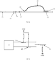
- FIG. 1 is a schematic diagram of a communication device board provided based on an example of the present disclosure, where the communication device board may be applied to a communication device.
- a connector of a communication device board 10 includes a fixed position 11 and a contact position 12, where a level of the fixed position 11 is different from a level of the contact position 12.
- the fixed position 11 is used to be fixedly connected to one end 21 of an inner side of a conductive resilient sheet 20 (e.g., a side close to the communication device board 10), where an outer side of the conductive resilient sheet 20 (e.g., a side facing away from the communication device board 10) is provided with an insulating coating.
- a conductive resilient sheet 20 e.g., a side close to the communication device board 10
- an outer side of the conductive resilient sheet 20 e.g., a side facing away from the communication device board 10.
- the level of the fixed position 11 is different from the level of the contact position 12, when one end 21 of the inner side of the conductive resilient sheet 20 is fixedly connected to the fixed position 11 and the other end 22 of the inner side of the conductive resilient sheet 20 is in contact with the contact position 12, the level of the fixed position 11 or the level of contact position 12 could be changed. Therefore, by detecting transitions of the level of the fixed position 11 or the level of the contact position 12, whether the other end 22 of the inner side of the conductive resilient sheet 20 is in contact with the contact position 12 could be determined. Further, whether the mating gap between the connector of the communication device board 10 and the corresponding connector in the communication device is smaller than the preset threshold range could be determined.
- the mating gap between the connector of the communication device board 10 and the corresponding connector in the communication device is smaller than the preset threshold range.
- FIG. 2 is a schematic diagram of a conductive resilient sheet provided based on an example of the present disclosure.
- the conductive resilient sheet 20 may be made of a metal conductive material, and the outer side of the conductive resilient sheet 20 is provided with an insulating coating.
- the conductive resilient sheet 20 may be deformed when subject to a force, and may be restored to an original state without being subjected to a force.
- one conductive end 21 of the inner side of the conductive resilient sheet 20 is fixedly connected to the fixed position 11 of the connector of the communication device board 10.
- the conductive resilient sheet 20 may be extended due to a force, and a position at which the other end 22 of the inner side of the conductive resilient sheet 20 is in contact with the connector of the communication device board 10 may also be changed.
- the other end 22 of the inner side of the conductive resilient sheet 20 may be in contact with the contact position 12 of the connector of the communication device board 10.
- FIG. 3A is a structural diagram of a communication device board provided based on an example of the present disclosure. As shown in FIG. 3A , on the basis of the communication device board shown in FIG. 2 , the communication device board 10 may also include a logic chip 15.
- the logic chip 15 is connected to the contact position 12, so as to detect a level state transition of the contact position 12 and generate a corresponding level transition signal.
- a circuit diagram, illustrating an operation principle of the communication device board 10 may be as shown in FIG. 3B , where the fixed position 11 of the connector of the communication device board 10 is grounded, and the contact position 12 of the connector is connected to a preset power supply.
- groundings refer to grounding through a resistor and all connections to a power supply refer to the power supply connected through a resistor, unless otherwise specified, which will not be repeated below in the examples of the present disclosure.
- the logic chip 15 detects that the contact position 12 is at a high level.
- the logic chip 15 may detect that the level of the contact position 12 changes from the high level to a low level and stays at the low level.
- a circuit diagram showing a working principle is shown in FIG. 3D .
- the logic chip 15 may generate a corresponding level transition signal (referred to as a first level transition signal), and a user (for example, an administrator) may determine that the communication device board 10 is properly plugged-in based on the first level transition signal.
- the first level transition signal generated by the logic chip 15 may be determined that an abnormality occurs during the insertion. At this time, corresponding measures may be taken based on actual situations.
- a region in which the other end 22 of the inner side of the conductive resilient sheet 20 is in contact with the connector of the communication device board 10 may gradually go close to the fixed position 11 from the contact position 12.
- the connector of the communication device board 10 is gradually separated from the corresponding connector in the communication device, and the mating gap of two connectors is gradually increased.
- the logic chip 15 may detect that the level of the contact position 12 changes from the low level to the high level and stays at the high level state.
- the logic chip 15 may generate a corresponding level transition signal (referred to as a second level transition signal), and a user (for example, an administrator) may determine that the communication device board 10 is unplugged based on the second level transition signal.
- a circuit diagram illustrating an operation principle of the communication device board may be as shown in FIG. 3E , where the fixed position 11 of the connector of the communication device board 10 is connected to a preset power supply, and the contact position 12 is grounded.
- the logic chip 15 detects that the contact position 12 is at a low level.
- the logic chip 15 may detect that the level of the contact position 12 changes from the low level to a high level and stays at the high level state.
- the logic chip 15 may generate a corresponding level transition signal (referred to as a third level transition signal), and a user (for example, an administrator) may determine that the communication device board 10 is properly inserted based on the third level transition signal.
- the third level transition signal generated by the logic chip 15 may be determined that an abnormality occurs during the insertion. At this time, corresponding measures may be taken based on an actual situation.
- the logic chip 15 may generate a corresponding level transition signal (referred to as a fourth level transition signal), and a user (for example, an administrator) may determine that the communication device board 10 is unplugged based on the fourth level transition signal.
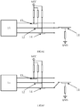
- FIG. 4A is a structural diagram of a communication device board provided based on an example of the present disclosure. As shown in FIG. 4A , on the basis of the communication device board shown in FIG. 3A , the communication device board 10 may also include a contact position 13, where a level of the contact position 13 is different from the level of the fixed position 11.
- the connector of the communication device board 10 may also include another contact position (e.g., the contact position 13 shown in FIG. 4A ), where the contact position 13 is closer to the fixed position 11 than the contact position 12.
- the contact position 13 and the fixed position 11 also have different levels.
- the logic chip 15 may be connected to the contact position 12 and the contact position 13 respectively, so as to detect level state changes of the contact position 12 and the contact position 13 and generate corresponding level transition signals.
- a circuit diagram illustrating an operation principle of the communication device board may be as shown in FIG. 4B , where the fixed position 11 of the connector of the communication device board 10 is grounded, and the contact position 12 and the contact position 13 are connected to a preset power supply.
- the logic chip 15 may detect that the contact position 13 is at a low level, and the contact position 12 is at a high level.
- the other end 22 of the inner side of the conductive resilient sheet 20 gradually goes close to the contact position 12 since the conductive resilient sheet 20 is subject to a force.
- the connector of the communication device board 10 is connected to the corresponding connector in the communication device to a certain extent, the other end 22 of the inner side of the conductive resilient sheet 20 is no longer in contact with the contact position 13, and the contact position 13 is disconnected with the fixed position 11.
- the logic chip 15 may detect that the level of the contact position 13 changes from the low level to a high level and stays at the high level state, while the contact position 12 still stays at the high level state.
- the logic chip 15 may generate a corresponding level transition signal (referred to as a fifth level transition signal), and a user (for example, an administrator) may determine that the connector of the communication device board 10 is already connected to the corresponding connector in the communication device, but does not yet complete the connection (e.g., in an under-mating state in which the mating gap between the connector of the communication device board 10 and the corresponding connector in the communication device is greater than an upper limit of a preset threshold range) based on the fifth level transition signal.
- a user for example, an administrator
- the connector of the communication device board 10 As the communication device board 10 is continuously inserted, the connector of the communication device board 10 is gradually and closely connected to the corresponding connector in the communication device and the other end 22 of the inner side of the conductive resilient sheet 20 continuously goes close to the contact position 12.
- the connector of the communication device board 10 When the connector of the communication device board 10 is properly connected to the corresponding connector in the communication device, that is, the mating gap between the connector of the communication device board 10 and the corresponding connector in the communication device reaches the preset threshold range, the other end 22 of the inner side of the conductive resilient sheet 20 is in contact with the contact position 12, and the contact position 12 is successfully connected to the fixed position 11, as shown in FIG. 4C .
- the logic chip 15 may detect that the level of the contact position 12 changes from the high level to a low level and stays at the low level state and the contact position 13 remains the high level state, a circuit diagram illustrating an operation principle of which may be as shown in FIG. 4D .
- the logic chip 15 may generate a corresponding level transition signal (referred to as a sixth level transition signal), and a user (for example, an administrator) may determine that the communication device board 10 is properly inserted based on the sixth level transition signal.
- level state changes of the contact position 12 and the contact position 13 when the communication device board 10 is unplugged are opposite to those when the communication device board 10 is inserted, and a specific implementation thereof will not be described herein.
- a circuit diagram illustrating an operation principle of a communication device board may be as shown in FIG. 4E , where the fixed position 11 of the connector of the communication device board 10 is connected to a preset power supply, and the contact position 12 and the contact position 13 are grounded.
- the logic chip 15 may detect that the contact position 13 is at a high level, and the contact position 12 is at a low level.
- the other end 22 of the inner side of the conductive resilient sheet 20 gradually goes close to the contact position 12 since the conductive resilient sheet 20 is subject to a force.
- the connector of the communication device board 10 is connected to the corresponding connector in the communication device to a certain extent, the other end 22 of the inner side of the conductive resilient sheet 20 is no longer in contact with the contact position 13, and the contact position 13 is disconnected with the fixed position 11.
- the logic chip 15 may detect that the level of the contact position 13 changes from the high level to a low level and stays at the low level state, while the contact position 12 still stays at the low level state.
- the logic chip 15 may generate a corresponding level transition signal (referred to as a seventh level transition signal), and a user (for example, an administrator) may determine that the connector of the communication device board 10 is already connected to the corresponding connector in the communication device, but does not yet complete the connection based on the seventh level transition signal.
- a user for example, an administrator
- the connector of the communication device board 10 As the communication device board 10 is continuously inserted, the connector of the communication device board 10 is gradually and closely connected to the corresponding connector in the communication device, and the other end 22 of the inner side of the conductive resilient sheet 20 continuously goes close to the contact position 12.
- the connector of the communication device board 10 When the connector of the communication device board 10 is properly connected to the corresponding connector in the communication device, that is, the mating gap between the connector of the communication device board 10 and the corresponding connector in the communication device reaches the preset threshold range, the other end 22 of the inner side of the conductive resilient sheet 20 is in contact with the contact position 12, and the contact position 12 is successfully connected to the fixed position 11.
- the logic chip 15 may detect that the level of the contact position 12 changes from the low level to a high level and stays at the low level state. The contact position 13 still remains the low level state.
- the logic chip 15 may generate a corresponding level transition signal (referred to as an eighth level transition signal), and a user (for example, an administrator) may determine that the communication device board 10 is properly inserted based on the eighth level transition signal.
- level state changes of the contact position 12 and the contact position 13 when the communication device board 10 is removed are opposite to those when the communication device board 10 is inserted, and a specific implementation thereof will not be described herein.
- whether the communication device board 10 is properly inserted or in the under-mating state may be determined by detecting the level changes of the contact position 12 and the contact position 13.
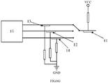
- FIG. 5A is a structural diagram of a communication device board provided based on an example of the present disclosure. As shown in FIG. 5A , on the basis of the communication device board shown in FIG. 3A , the communication device board 10 may also include a contact position 14, where a level of the contact position 14 is different with a level of the fixed position 11.
- the connector of the communication device board 10 may also include another contact position (e.g., the contact position 14 shown in FIG. 5A ).
- the contact position 14 is farther from the fixed position 11 than the contact position 12, and the contact position 14 and the fixed position 11 also have different levels.
- the logic chip 15 may be connected to the contact position 12 and the contact position 14 respectively, so as to detect level state changes of the contact position 12 and the contact position 14 and generate corresponding level transition signals.
- FIG. 5B a circuit diagram illustrating an operation principle of the communication device board may be shown in FIG. 5B , where the fixed position 11 of the connector of the communication device board 10 is grounded, and the contact position 12 and the contact position 14 are connected to a preset power supply.
- the logic chip 15 may detect that the level of the contact position 12 changes from a high level to a low level and stays at the low level state, and the contact position 14 is still at a high level.
- the logic chip 15 may generate a corresponding level transition signal (referred to as a ninth level transition signal), and a user (for example, an administrator) may determine that the communication device board 10 is properly inserted based on the ninth level transition signal.
- the other end 22 of the inner side of the conductive resilient sheet 20 may gradually go close to the contact position 14.
- the connector of the communication device board 10 and the corresponding connector in the communication device are in an over-mating state (that is, the mating gap between the connector of the communication device board 10 and the corresponding connector in the communication device is less than the lower limit of the preset threshold range)
- the other end 22 of the inner side of the conductive resilient sheet 20 is no longer in contact with the contact position 12, but changes to be in contact with the contact position 14.
- the contact position 14 is successfully connected to the fixed position 11, as shown in FIG. 5E .
- the logic chip 15 may detect that the level of the contact position 14 changes from the high level to a low level and stays at the low level state and the contact position 12 changes to the high level.
- a circuit diagram of which may be as shown in FIG. 5F .
- the logic chip 15 may generate a corresponding level transition signal (referred to as a tenth level transition signal), and a user (for example, an administrator) may determine that the communication device board 10 is inserted too tightly based on the tenth level transition signal.
- level state changes of the contact position 12 and the contact position 14 when the communication device board 10 is removed are opposite to those when the communication device board 10 is inserted, and a specific implementation thereof will not be described herein.
- a circuit diagram of the communication device board may be as shown in FIG. 5G , where the fixed position 11 of the connector of the communication device board 10 is connected to a preset power supply, and the contact position 12 and the contact position 14 are grounded.
- level state changes of the contact position 12 and the contact position 14 are opposite to those when the communication device board 10 is inserted in the above manner, and a specific implementation thereof will not be described herein.
- the level state changes of the contact position 12 and the contact position 14 are opposite to the level state changes of the contact position 12 and the contact position when the communication device board 10 is removed in the above manner, and a specific implementation thereof will not be described herein.
- FIG. 6A is a structural diagram of a communication device board provided based on an example of the present disclosure.
- the communication device board 10 may also include a contact position 13 and a contact position 14, where a level of the contact position 13 is different from a level of the fixed position 11 and a level of the contact position 14 is also different from the level of the fixed position 11.
- a circuit diagram illustrating an operation principle of the communication device board may be as shown in FIG. 6B , where the fixed position 11 of the connector of the communication device board 10 is grounded, and the contact position 12, the contact position 13 and the contact position 14 are connected to a preset power supply.
- FIG. 6A when the communication device board 10 is inserted, situations for contact between the other end 22 of the inner side of the conductive resilient sheet 20 and the connector of the communication device board 10 are shown in FIG. 6A , FIG. 6C and FIG. 6D respectively.
- Connection relationships of the circuit diagrams of the communication device board 10 may be as shown in FIG 6B , FIG. 6E and FIG. 6F respectively, where FIG. 6A corresponds to FIG. 6B, FIG. 6C corresponds to FIG. 6E , and FIG. 6D corresponds to FIG. 6F .
- level state changes of the contact position 12, the contact position 13 and the contact position 14 when the communication device board 10 is unplugged are opposite to those when the communication device board 10 is inserted, and a specific implementation thereof will not be described herein.
- a circuit diagram illustrating an operation principle of the communication device board may be as shown in FIG. 6G , where the fixed position 11 of the connector of the communication device board 10 is connected to a preset power supply, and the contact position 12, the contact position 13 and the contact position 14 are grounded.
- whether the communication device board is properly inserted, in the over-mating state, or in the under-mating state may be determined by detecting the level changes of the contact position 12, the contact position 13 and the contact position 14.
- the logic chip 15 may generate a corresponding level transition signal based on the detected level change of each of the contact positions, and then store the level transition signal in a register.
- the corresponding level transition signal may be read from the register by controlling a Center Process Unit (CPU) by a user (for example, an administrator) through corresponding control instructions, and displayed to the user for viewing, so as to accurately obtain the insertion condition of the communication device board.
- CPU Center Process Unit
- the logic chip 15 may directly output the level transition signal, for example, output the generated level transition signal to a CPU.
- the CPU may display the signal to a user in a specified functional interface, so that the user may accurately obtain the insertion condition of the communication device board.
- the fixed position and the contact position with different levels may be arranged on the connector of the communication device board, and the fixed position of the connector of the communication device board is fixedly connected to one end of the inner side of the conductive resilient sheet.
- the mating gap between the connector of the communication device board and the corresponding connector in the communication device is smaller than the preset threshold range, the other end of the inner side of the conductive resilient sheet is in contact with the contact position 12. In this way, whether the communication device board is properly inserted may be determined based on the level change of the contact position 12.
- an example of the present disclosure also provides a communication device, which may include a communication device board described in any one of the above examples.
Landscapes
- Engineering & Computer Science (AREA)
- Microelectronics & Electronic Packaging (AREA)
- Computer Hardware Design (AREA)
- General Engineering & Computer Science (AREA)
- Details Of Connecting Devices For Male And Female Coupling (AREA)
- Mounting Of Printed Circuit Boards And The Like (AREA)
Abstract
Description
- This application claims priority to Chinese Patent Application No.
201710882782.X - A rack with insertion and removal module may refer to a rack with modular design in which all modules such as service boards, main control boards, network boards, fans and power supply(s) are independent. Signals between the modules are transmitted through connectors and the modules are fixed through structural parts to form a system.
- In the rack, a circuit board of a module can be fixed in a handle bar component which has a tray structure. The handle bar component can be fastened and pulled out by levers which are on the handle bar component. Thus, modules of the rack are insertion and removal, the configuration of the modules in rack is flexible. The rack supports redundant modules, and it is convenient to repair and maintain the modules in the rack.
- An existing rack with insertion and removal module may be assembled by fastening the handle bar component and tightening a screw into an outer side of a structural part so as to ensure that a mating gap between the modules satisfies requirements.
-
-
FIG. 1 is a schematic diagram of a communication device board provided based on an example of the present disclosure. -
FIG. 2 is a schematic diagram of a conductive resilient sheet provided based an example of the present disclosure. -
FIGS. 3A-3E are schematic diagrams and circuit diagrams of a communication device board based on a first example. -
FIGS. 4A-4E are schematic diagrams and circuit diagrams of a communication device board based on a second example. -
FIGS. 5A-5G are schematic diagrams and circuit diagrams of a communication device board based on a third example. -
FIGS. 6A-6G are schematic diagrams and circuit diagrams of a communication device board based on a fourth example. - To enable persons skilled in the art to better understand technical solutions in examples of the present disclosure and make the above objects, characteristics and advantages of the examples of the present disclosure more apparent and intelligible, the technical solutions in the examples of the present disclosure will be further described in detail below in conjunction with accompanying drawings.
- In an assembling manner of an existing rack with insertion and removal module, actual connection positions between modules, e.g., connectors between modules, are located in a chassis. Thus, it is very difficult to determine whether a mating gap between modules reaches a design requirement only by external observation. In view of this, the present disclosure discloses a communication device board and a communication device to solve the technical problem.
-
FIG. 1 is a schematic diagram of a communication device board provided based on an example of the present disclosure, where the communication device board may be applied to a communication device. As shown inFIG. 1 , a connector of acommunication device board 10 includes afixed position 11 and acontact position 12, where a level of thefixed position 11 is different from a level of thecontact position 12. - The
fixed position 11 is used to be fixedly connected to oneend 21 of an inner side of a conductive resilient sheet 20 (e.g., a side close to the communication device board 10), where an outer side of the conductive resilient sheet 20 (e.g., a side facing away from the communication device board 10) is provided with an insulating coating. - When the
fixed position 11 is fixedly connected to theend 21 of the inner side of the conductiveresilient sheet 20 and a mating gap between a connector of thecommunication device board 10 and a corresponding connector in a rack is smaller than a preset threshold range, theother end 22 of the inner side of the conductiveresilient sheet 20 is in contact with thecontact position 12. - In an example of the present disclosure, since the level of the
fixed position 11 is different from the level of thecontact position 12, when oneend 21 of the inner side of the conductiveresilient sheet 20 is fixedly connected to thefixed position 11 and theother end 22 of the inner side of the conductiveresilient sheet 20 is in contact with thecontact position 12, the level of thefixed position 11 or the level ofcontact position 12 could be changed. Therefore, by detecting transitions of the level of thefixed position 11 or the level of thecontact position 12, whether theother end 22 of the inner side of the conductiveresilient sheet 20 is in contact with thecontact position 12 could be determined. Further, whether the mating gap between the connector of thecommunication device board 10 and the corresponding connector in the communication device is smaller than the preset threshold range could be determined. - When the connector of the
communication device board 10 and the corresponding connector in the communication device are properly connected, that is, thecommunication device board 10 is properly plugged-in, the mating gap between the connector of thecommunication device board 10 and the corresponding connector in the communication device is smaller than the preset threshold range. -
FIG. 2 is a schematic diagram of a conductive resilient sheet provided based on an example of the present disclosure. The conductiveresilient sheet 20 may be made of a metal conductive material, and the outer side of the conductiveresilient sheet 20 is provided with an insulating coating. The conductiveresilient sheet 20 may be deformed when subject to a force, and may be restored to an original state without being subjected to a force. - Correspondingly, one
conductive end 21 of the inner side of the conductiveresilient sheet 20 is fixedly connected to thefixed position 11 of the connector of thecommunication device board 10. When thecommunication device board 10 is plugged into the communication device, as the connector of thecommunication device board 10 and the corresponding connector in the communication device are gradually tightened, the conductiveresilient sheet 20 may be extended due to a force, and a position at which theother end 22 of the inner side of the conductiveresilient sheet 20 is in contact with the connector of thecommunication device board 10 may also be changed. When thecommunication device board 10 is properly plugged-in, that is, the mating gap between the connector of thecommunication device board 10 and the corresponding connector in the communication device reaches the preset threshold range, theother end 22 of the inner side of the conductiveresilient sheet 20 may be in contact with thecontact position 12 of the connector of thecommunication device board 10. - To enable persons skilled in the art to better understand technical solutions of examples of the present disclosure, the technical solutions of examples of the present disclosure will be described below in conjunction with the specific examples.
-
FIG. 3A is a structural diagram of a communication device board provided based on an example of the present disclosure. As shown inFIG. 3A , on the basis of the communication device board shown inFIG. 2 , thecommunication device board 10 may also include alogic chip 15. - The
logic chip 15 is connected to thecontact position 12, so as to detect a level state transition of thecontact position 12 and generate a corresponding level transition signal. - In one manner of the example, a circuit diagram, illustrating an operation principle of the
communication device board 10, may be as shown inFIG. 3B , where thefixed position 11 of the connector of thecommunication device board 10 is grounded, and thecontact position 12 of the connector is connected to a preset power supply. - It is to be noted that, in examples of the present disclosure, all mentioned groundings refer to grounding through a resistor and all connections to a power supply refer to the power supply connected through a resistor, unless otherwise specified, which will not be repeated below in the examples of the present disclosure.
- In this manner, when the connector of the
communication device board 10 is not connected with the corresponding connector in the communication device, theother end 22 of the inner side of the conductiveresilient sheet 20 is in contact with a region (a region is located between thefixed position 11 and the contact position 12) other than thecontact position 12 of the connector of thecommunication device board 10. At this time, thelogic chip 15 detects that thecontact position 12 is at a high level. - When the
communication device board 10 is plugged into the communication device and the connector of thecommunication device board 10 is gradually and closely connected to the corresponding connector in the communication device, theother end 22 of the inner side of the conductiveresilient sheet 20 gradually goes close to thecontact position 12 since the conductiveresilient sheet 20 is subject to a force. When the connector of thecommunication device board 10 is properly connected to the corresponding connector in the communication device, that is, the mating gap of the connector of thecommunication device board 10 and the corresponding connector in the communication device reaches a preset threshold range, theother end 22 of the inner side of the conductiveresilient sheet 20 is in contact with thecontact position 12, and thecontact position 12 is successfully connected to thefixed position 11, as illustrated inFIG. 3C . At this time, thelogic chip 15 may detect that the level of thecontact position 12 changes from the high level to a low level and stays at the low level. A circuit diagram showing a working principle is shown inFIG. 3D . - When detecting a transition of the level of the
contact position 12 from the high level to the low level, thelogic chip 15 may generate a corresponding level transition signal (referred to as a first level transition signal), and a user (for example, an administrator) may determine that thecommunication device board 10 is properly plugged-in based on the first level transition signal. - It is to be noted that if the first level transition signal generated by the
logic chip 15 is not detected when thecommunication device board 10 is inserted, it may be determined that an abnormality occurs during the insertion. At this time, corresponding measures may be taken based on actual situations. - In this manner, when the
communication device board 10 in a normal working state is unplugged (man-made or malfunction), a region in which theother end 22 of the inner side of the conductiveresilient sheet 20 is in contact with the connector of thecommunication device board 10 may gradually go close to thefixed position 11 from thecontact position 12. As thecommunication device board 10 is unplugged, the connector of thecommunication device board 10 is gradually separated from the corresponding connector in the communication device, and the mating gap of two connectors is gradually increased. When the mating gap between the connector of thecommunication device board 10 and the corresponding connector in the communication device exceeds an upper limit of the preset threshold range, theother end 22 of the inner side of the conductiveresilient sheet 20 is no longer in contact with thecontact position 12, and thecontact position 12 is disconnected with thefixed position 11. At this time, thelogic chip 15 may detect that the level of thecontact position 12 changes from the low level to the high level and stays at the high level state. - When detecting a transition of the level of the
contact position 12 from the low level to the high level, thelogic chip 15 may generate a corresponding level transition signal (referred to as a second level transition signal), and a user (for example, an administrator) may determine that thecommunication device board 10 is unplugged based on the second level transition signal. - In another manner of the example, a circuit diagram illustrating an operation principle of the communication device board may be as shown in
FIG. 3E , where the fixedposition 11 of the connector of thecommunication device board 10 is connected to a preset power supply, and thecontact position 12 is grounded. - In this manner, when the connector of the
communication device board 10 is not connected to the corresponding connector in the communication device, theother end 22 of the inner side of the conductiveresilient sheet 20 is in contact with a region other than thecontact position 12 of the connector of thecommunication device board 10. At this time, thelogic chip 15 detects that thecontact position 12 is at a low level. - When the
communication device board 10 is inserted into the communication device and the connector of thecommunication device board 10 is gradually and closely connected to the corresponding connector in the communication device, theother end 22 of the inner side of the conductiveresilient sheet 20 gradually goes close to thecontact position 12 since the conductiveresilient sheet 20 is subject to a force. When the connector of thecommunication device board 10 is properly connected to the corresponding connector in the communication device, that is, when the mating gap between the connector of thecommunication device board 10 and the corresponding connector in the communication device reaches a preset threshold range, theother end 22 of the inner side of the conductiveresilient sheet 20 is in contact with thecontact position 12, and thecontact position 12 is successfully connected with the fixedposition 11. At this time, thelogic chip 15 may detect that the level of thecontact position 12 changes from the low level to a high level and stays at the high level state. - When detecting a transition of the level of the
contact position 12 from the low level to the high level, thelogic chip 15 may generate a corresponding level transition signal (referred to as a third level transition signal), and a user (for example, an administrator) may determine that thecommunication device board 10 is properly inserted based on the third level transition signal. - It is to be noted that if the third level transition signal generated by the
logic chip 15 is not detected when thecommunication device board 10 is inserted, it may be determined that an abnormality occurs during the insertion. At this time, corresponding measures may be taken based on an actual situation. - In this manner, when the
communication device board 10 in a normal working state is unplugged (man-made or malfunction), a region in which theother end 22 of the inner side of the conductiveresilient sheet 20 is in contact with the connector of thecommunication device board 10 may gradually go close to the fixedposition 11 from thecontact position 12. As thecommunication device board 10 is unplugged, the connector of thecommunication device board 10 is gradually separated from the corresponding connector in the communication device, and the mating gap of two connectors is gradually increased. When the mating gap between the connector of thecommunication device board 10 and the corresponding connector in the communication device exceeds an upper limit of the preset threshold range, theother end 22 of the inner side of the conductiveresilient sheet 20 is no longer in contact with thecontact position 12, and thecontact position 12 is disconnected with the fixedposition 11. At this time, thelogic chip 15 may detect that the level of thecontact position 12 changes from the high level to the low level and stays at the low level state. - When detecting a transition of the level of the
contact position 12 from the high level to the low level, thelogic chip 15 may generate a corresponding level transition signal (referred to as a fourth level transition signal), and a user (for example, an administrator) may determine that thecommunication device board 10 is unplugged based on the fourth level transition signal. - Therefore, in this manner, whether the communication device board is properly inserted or unplugged may be determined by detecting a level change of the
contact position 12. -
FIG. 4A is a structural diagram of a communication device board provided based on an example of the present disclosure. As shown inFIG. 4A , on the basis of the communication device board shown inFIG. 3A , thecommunication device board 10 may also include acontact position 13, where a level of thecontact position 13 is different from the level of the fixedposition 11. - When the fixed
position 11 is fixedly connected to oneend 21 of the inner side of the conductiveresilient sheet 20 and the mating gap between the connector of thecommunication device board 10 and the corresponding connector in the communication device is greater than an upper limit of a preset threshold range, theother end 22 of the inner side of the conductiveresilient sheet 20 is in contact with thecontact position 13. - In this example, to obtain a mating state between the connector of the
communication device board 10 and the corresponding connector in the communication device more accurately, the connector of thecommunication device board 10 may also include another contact position (e.g., thecontact position 13 shown inFIG. 4A ), where thecontact position 13 is closer to the fixedposition 11 than thecontact position 12. Thecontact position 13 and the fixedposition 11 also have different levels. - Correspondingly, the
logic chip 15 may be connected to thecontact position 12 and thecontact position 13 respectively, so as to detect level state changes of thecontact position 12 and thecontact position 13 and generate corresponding level transition signals. - In one manner of the example, a circuit diagram illustrating an operation principle of the communication device board may be as shown in
FIG. 4B , where the fixedposition 11 of the connector of thecommunication device board 10 is grounded, and thecontact position 12 and thecontact position 13 are connected to a preset power supply. - In this manner, when the connector of the
communication device board 10 is not connected to the corresponding connector in the communication device, theother end 22 of the inner side of the conductiveresilient sheet 20 is in contact with thecontact position 13 of the connector of thecommunication device board 10 as shown inFIG. 4A . At this time, thelogic chip 15 may detect that thecontact position 13 is at a low level, and thecontact position 12 is at a high level. - When the
communication device board 10 is plugged into the communication device and the connector of thecommunication device board 10 begins to connect to the corresponding connector in the communication device, theother end 22 of the inner side of the conductiveresilient sheet 20 gradually goes close to thecontact position 12 since the conductiveresilient sheet 20 is subject to a force. When the connector of thecommunication device board 10 is connected to the corresponding connector in the communication device to a certain extent, theother end 22 of the inner side of the conductiveresilient sheet 20 is no longer in contact with thecontact position 13, and thecontact position 13 is disconnected with the fixedposition 11. Thelogic chip 15 may detect that the level of thecontact position 13 changes from the low level to a high level and stays at the high level state, while thecontact position 12 still stays at the high level state. - When detecting a transition of the level of the
contact position 13 from the low level to the high level, thelogic chip 15 may generate a corresponding level transition signal (referred to as a fifth level transition signal), and a user (for example, an administrator) may determine that the connector of thecommunication device board 10 is already connected to the corresponding connector in the communication device, but does not yet complete the connection (e.g., in an under-mating state in which the mating gap between the connector of thecommunication device board 10 and the corresponding connector in the communication device is greater than an upper limit of a preset threshold range) based on the fifth level transition signal. - As the
communication device board 10 is continuously inserted, the connector of thecommunication device board 10 is gradually and closely connected to the corresponding connector in the communication device and theother end 22 of the inner side of the conductiveresilient sheet 20 continuously goes close to thecontact position 12. When the connector of thecommunication device board 10 is properly connected to the corresponding connector in the communication device, that is, the mating gap between the connector of thecommunication device board 10 and the corresponding connector in the communication device reaches the preset threshold range, theother end 22 of the inner side of the conductiveresilient sheet 20 is in contact with thecontact position 12, and thecontact position 12 is successfully connected to the fixedposition 11, as shown inFIG. 4C . At this time, thelogic chip 15 may detect that the level of thecontact position 12 changes from the high level to a low level and stays at the low level state and thecontact position 13 remains the high level state, a circuit diagram illustrating an operation principle of which may be as shown inFIG. 4D . - When detecting a transition of the level of the
contact position 12 from the high level to the low level, thelogic chip 15 may generate a corresponding level transition signal (referred to as a sixth level transition signal), and a user (for example, an administrator) may determine that thecommunication device board 10 is properly inserted based on the sixth level transition signal. - It is to be noted that in this manner, level state changes of the
contact position 12 and thecontact position 13 when thecommunication device board 10 is unplugged are opposite to those when thecommunication device board 10 is inserted, and a specific implementation thereof will not be described herein. - In another manner of the example, a circuit diagram illustrating an operation principle of a communication device board may be as shown in
FIG. 4E , where the fixedposition 11 of the connector of thecommunication device board 10 is connected to a preset power supply, and thecontact position 12 and thecontact position 13 are grounded. - In this manner, when the connector of the
communication device board 10 is not connected to the corresponding connector in the communication device, theother end 22 of the inner side of the conductiveresilient sheet 20 is in contact with thecontact position 13 of the connector of thecommunication device board 10. At this time, thelogic chip 15 may detect that thecontact position 13 is at a high level, and thecontact position 12 is at a low level. - When the
communication device board 10 is plugged into the communication device and the connector of thecommunication device board 10 begins to connect to the corresponding connector in the communication device, theother end 22 of the inner side of the conductiveresilient sheet 20 gradually goes close to thecontact position 12 since the conductiveresilient sheet 20 is subject to a force. When the connector of thecommunication device board 10 is connected to the corresponding connector in the communication device to a certain extent, theother end 22 of the inner side of the conductiveresilient sheet 20 is no longer in contact with thecontact position 13, and thecontact position 13 is disconnected with the fixedposition 11. Thelogic chip 15 may detect that the level of thecontact position 13 changes from the high level to a low level and stays at the low level state, while thecontact position 12 still stays at the low level state. - When detecting a transition of the level of the
contact position 13 from the high level to the low level, thelogic chip 15 may generate a corresponding level transition signal (referred to as a seventh level transition signal), and a user (for example, an administrator) may determine that the connector of thecommunication device board 10 is already connected to the corresponding connector in the communication device, but does not yet complete the connection based on the seventh level transition signal. - As the
communication device board 10 is continuously inserted, the connector of thecommunication device board 10 is gradually and closely connected to the corresponding connector in the communication device, and theother end 22 of the inner side of the conductiveresilient sheet 20 continuously goes close to thecontact position 12. When the connector of thecommunication device board 10 is properly connected to the corresponding connector in the communication device, that is, the mating gap between the connector of thecommunication device board 10 and the corresponding connector in the communication device reaches the preset threshold range, theother end 22 of the inner side of the conductiveresilient sheet 20 is in contact with thecontact position 12, and thecontact position 12 is successfully connected to the fixedposition 11. At this time, thelogic chip 15 may detect that the level of thecontact position 12 changes from the low level to a high level and stays at the low level state. Thecontact position 13 still remains the low level state. - When detecting a transition of the level of the
contact position 12 from the high level to the low level, thelogic chip 15 may generate a corresponding level transition signal (referred to as an eighth level transition signal), and a user (for example, an administrator) may determine that thecommunication device board 10 is properly inserted based on the eighth level transition signal. - It is to be noted that in this manner, level state changes of the
contact position 12 and thecontact position 13 when thecommunication device board 10 is removed are opposite to those when thecommunication device board 10 is inserted, and a specific implementation thereof will not be described herein. - Thus, in this example, whether the
communication device board 10 is properly inserted or in the under-mating state may be determined by detecting the level changes of thecontact position 12 and thecontact position 13. -
FIG. 5A is a structural diagram of a communication device board provided based on an example of the present disclosure. As shown inFIG. 5A , on the basis of the communication device board shown inFIG. 3A , thecommunication device board 10 may also include acontact position 14, where a level of thecontact position 14 is different with a level of the fixedposition 11. - When the fixed
position 11 is fixedly connected to oneend 21 of the inner side of the conductiveresilient sheet 20 and the mating gap between the connector of thecommunication device board 10 and the corresponding connector in the communication device is less than a lower limit of a preset threshold range, theother end 22 of the inner side of the conductiveresilient sheet 20 is in contact with thecontact position 14. - In this example, to obtain a mating state between the connector of the
communication device board 10 and the corresponding connector in the communication device more accurately, the connector of thecommunication device board 10 may also include another contact position (e.g., thecontact position 14 shown inFIG. 5A ). Thecontact position 14 is farther from the fixedposition 11 than thecontact position 12, and thecontact position 14 and the fixedposition 11 also have different levels. - Correspondingly, the
logic chip 15 may be connected to thecontact position 12 and thecontact position 14 respectively, so as to detect level state changes of thecontact position 12 and thecontact position 14 and generate corresponding level transition signals. - In one manner of the example, a circuit diagram illustrating an operation principle of the communication device board may be shown in
FIG. 5B , where the fixedposition 11 of the connector of thecommunication device board 10 is grounded, and thecontact position 12 and thecontact position 14 are connected to a preset power supply. - In this manner, when the
communication device board 10 is inserted into the communication device and the connector of thecommunication device board 10 is gradually and closely connected to the corresponding connector in the communication device, theother end 22 of the inner side of the conductiveresilient sheet 20 gradually goes close to thecontact position 12 since the conductiveresilient sheet 20 is subject to a force. When the connector of thecommunication device board 10 is properly connected to the corresponding connector in the communication device, that is, the mating gap between the connector of thecommunication device board 10 and the corresponding connector in the communication device reaches the preset threshold range, theother end 22 of the inner side of the conductiveresilient sheet 20 is in contact with thecontact position 12, and thecontact position 12 is successfully connected to the fixedposition 11, as shown inFIG. 5C . At this time, thelogic chip 15 may detect that the level of thecontact position 12 changes from a high level to a low level and stays at the low level state, and thecontact position 14 is still at a high level. A circuit diagram of which may be shown inFIG. 5D . - When detecting a transition of the level of the
contact position 12 from the high level to the low level, thelogic chip 15 may generate a corresponding level transition signal (referred to as a ninth level transition signal), and a user (for example, an administrator) may determine that thecommunication device board 10 is properly inserted based on the ninth level transition signal. - In this manner, if the user (for example, the administrator) continues to insert the
communication device board 10 after it is properly inserted, theother end 22 of the inner side of the conductiveresilient sheet 20 may gradually go close to thecontact position 14. When the connector of thecommunication device board 10 and the corresponding connector in the communication device are in an over-mating state (that is, the mating gap between the connector of thecommunication device board 10 and the corresponding connector in the communication device is less than the lower limit of the preset threshold range), theother end 22 of the inner side of the conductiveresilient sheet 20 is no longer in contact with thecontact position 12, but changes to be in contact with thecontact position 14. At this time, thecontact position 14 is successfully connected to the fixedposition 11, as shown inFIG. 5E . At this time, thelogic chip 15 may detect that the level of thecontact position 14 changes from the high level to a low level and stays at the low level state and thecontact position 12 changes to the high level. A circuit diagram of which may be as shown inFIG. 5F . - When detecting a transition of the level of the
contact position 14 from the high level to the low level, thelogic chip 15 may generate a corresponding level transition signal (referred to as a tenth level transition signal), and a user (for example, an administrator) may determine that thecommunication device board 10 is inserted too tightly based on the tenth level transition signal. - It is to be noted that in this manner, level state changes of the
contact position 12 and thecontact position 14 when thecommunication device board 10 is removed are opposite to those when thecommunication device board 10 is inserted, and a specific implementation thereof will not be described herein. - In another manner of the example, a circuit diagram of the communication device board may be as shown in
FIG. 5G , where the fixedposition 11 of the connector of thecommunication device board 10 is connected to a preset power supply, and thecontact position 12 and thecontact position 14 are grounded. - In this manner, when the
communication device board 10 is inserted, level state changes of thecontact position 12 and thecontact position 14 are opposite to those when thecommunication device board 10 is inserted in the above manner, and a specific implementation thereof will not be described herein. Similarly, when thecommunication device board 10 is removed, the level state changes of thecontact position 12 and thecontact position 14 are opposite to the level state changes of thecontact position 12 and the contact position when thecommunication device board 10 is removed in the above manner, and a specific implementation thereof will not be described herein. - Therefore, in this manner, whether the communication device board is properly inserted or in the over-mating state may be determined by detecting the level changes of the
contact position 12 and thecontact position 14. -
FIG. 6A is a structural diagram of a communication device board provided based on an example of the present disclosure. As shown inFIG. 6A , on the basis of the communication device board shown inFIG. 3A , thecommunication device board 10 may also include acontact position 13 and acontact position 14, where a level of thecontact position 13 is different from a level of the fixedposition 11 and a level of thecontact position 14 is also different from the level of the fixedposition 11. - When the fixed
position 11 is fixedly connected to oneend 21 of the inner side of the conductiveresilient sheet 20 and the mating gap between the connector of thecommunication device board 10 and the corresponding connector in the communication device is greater than an upper limit of a preset threshold range, theother end 22 of the inner side of the conductiveresilient sheet 20 is in contact with thecontact position 13. - When the fixed
position 11 is fixedly connected to oneend 21 of the inner side of the conductiveresilient sheet 20 and the mating gap between the connector of thecommunication device board 10 and the corresponding connector in the communication device is less than a lower limit of the preset threshold range, theother end 22 of the inner side of the conductiveresilient sheet 20 is in contact with thecontact position 14. - In a manner of the example, a circuit diagram illustrating an operation principle of the communication device board may be as shown in
FIG. 6B , where the fixedposition 11 of the connector of thecommunication device board 10 is grounded, and thecontact position 12, thecontact position 13 and thecontact position 14 are connected to a preset power supply. - In this manner, when the
communication device board 10 is inserted, situations for contact between theother end 22 of the inner side of the conductiveresilient sheet 20 and the connector of thecommunication device board 10 are shown inFIG. 6A ,FIG. 6C and FIG. 6D respectively. Connection relationships of the circuit diagrams of thecommunication device board 10 may be as shown inFIG 6B ,FIG. 6E and FIG. 6F respectively, whereFIG. 6A corresponds toFIG. 6B, FIG. 6C corresponds toFIG. 6E , andFIG. 6D corresponds toFIG. 6F . - When the
communication device board 10 is inserted, a level change of each of the contact positions 12, 13 and 14 may be referred to the related descriptions in Example 2 and Example 3 respectively, which will not be described in this example of the present disclosure. - It is to be noted that level state changes of the
contact position 12, thecontact position 13 and thecontact position 14 when thecommunication device board 10 is unplugged are opposite to those when thecommunication device board 10 is inserted, and a specific implementation thereof will not be described herein. - In another manner of the example, a circuit diagram illustrating an operation principle of the communication device board may be as shown in
FIG. 6G , where the fixedposition 11 of the connector of thecommunication device board 10 is connected to a preset power supply, and thecontact position 12, thecontact position 13 and thecontact position 14 are grounded. - In this manner, when the
communication device board 10 is inserted, level state changes of thecontact position 12, thecontact position 13 and thecontact position 14 are opposite to those when thecommunication device board 10 is inserted in the above manner, and a specific implementation will not be described herein. Similarly, when thecommunication device board 10 is removed, level state changes of thecontact position 12, thecontact position 13 and thecontact position 14 are opposite to those when thecommunication device board 10 is removed in the above manner, and a specific implementation will not be described herein. - Therefore, in this example, whether the communication device board is properly inserted, in the over-mating state, or in the under-mating state may be determined by detecting the level changes of the
contact position 12, thecontact position 13 and thecontact position 14. - It shall be understood that all of the above examples are merely several specific examples illustrating arrangement of contact positions on the connector of the
communication device board 10, but do not limit the scope of protection of the present disclosure. In examples of the present disclosure, four or more contact positions may also be arranged on the connector of thecommunication device board 10 to obtain insertion condition of thecommunication device board 10 more accurately by detecting a level change of each of the contact positions, and a specific implementation thereof will not be described herein. - In an example of the present disclosure, the
logic chip 15 may generate a corresponding level transition signal based on the detected level change of each of the contact positions, and then store the level transition signal in a register. The corresponding level transition signal may be read from the register by controlling a Center Process Unit (CPU) by a user (for example, an administrator) through corresponding control instructions, and displayed to the user for viewing, so as to accurately obtain the insertion condition of the communication device board. - In another example of the present disclosure, after generating a level transition signal based on the detected level change of each of the contact positions, the
logic chip 15 may directly output the level transition signal, for example, output the generated level transition signal to a CPU. The CPU may display the signal to a user in a specified functional interface, so that the user may accurately obtain the insertion condition of the communication device board. - It may be seen from the above description that, in the technical solutions of the examples of the present disclosure, the fixed position and the contact position with different levels may be arranged on the connector of the communication device board, and the fixed position of the connector of the communication device board is fixedly connected to one end of the inner side of the conductive resilient sheet. When the mating gap between the connector of the communication device board and the corresponding connector in the communication device is smaller than the preset threshold range, the other end of the inner side of the conductive resilient sheet is in contact with the
contact position 12. In this way, whether the communication device board is properly inserted may be determined based on the level change of thecontact position 12. - Further, an example of the present disclosure also provides a communication device, which may include a communication device board described in any one of the above examples.
- After considering the specification and practicing the present disclosure, the persons of skill in the prior art may easily conceive of other implementations of the present disclosure. The present disclosure is intended to include any variations, uses and adaptive changes of the present disclosure. These variations, uses and adaptive changes follow the general principle of the present disclosure and include common knowledge or conventional technical means in the prior art not disclosed in the present disclosure. The specification and examples herein are intended to be illustrative only and the real scope and spirit of the present disclosure are indicated by the claims of the present disclosure.
- It is to be understood that the present disclosure is not limited to the precise structures described above and shown in the accompanying drawings and may be modified or changed without departing from the scope of the present disclosure. The scope of protection of the present disclosure is limited only by the appended claims.
Claims (8)
- A communication device board (10), applied to a communication device, comprising:a connector of the communication device board comprises a fixed position (11) and a first contact position (12), wherein a level of the fixed position (11) is different from a level of the first contact position (12);the fixed position (11) is fixedly connected to a first end (21) of an inner side of a conductive resilient sheet, wherein an outer side of the conductive resilient sheet is provided with an insulating coating;when the fixed position (11) is fixedly connected to the first end (21) of the inner side of the conductive resilient sheet and a mating gap between the connector of the communication device board and a corresponding communication device connector is smaller than a preset threshold range, a second end (22) of the inner side of the conductive resilient sheet is in contact with the first contact position (12).
- The communication device board according to claim 1, wherein
the connector of the communication device board comprises a second contact position (13), wherein a level of the second contact position (13) is different from the level of the fixed position (11);
when the fixed position (11) is fixedly connected to the first end (21) of the inner side of the conductive resilient sheet and the mating gap between the connector of the communication device board and the corresponding communication device connector is larger than an upper limit of the preset threshold range, the second end (22) of the inner side of the conductive resilient sheet is in contact with the second contact position (13). - The communication device board according to claim 1 or claim 2, wherein
the connector of the communication device board comprises a third contact position (14), wherein a level of the third contact position (14) is different from the level of the fixed position (11);
when the fixed position (11) is fixedly connected to the first end (21) of the inner side of the conductive resilient sheet and the mating gap between the connector of the communication device board and the corresponding communication device connector is smaller than a lower limit of the preset threshold range, the second end (22) of the inner side of the conductive resilient sheet is in contact with the third contact position (14). - The communication device board according to claim 1, further comprises a logic chip (15), wherein
the logic chip (15) is connected to the first contact position (12) and configured to detect level transitions of the first contact position (12) and generate different level transition signals. - The communication device board according to claim 4, wherein
the fixed position (11) connects to a preset power supply, and the first contact position (12) connects to ground;
the logic chip (15) connects to the first contact position (12); and
the logic chip (15) is to generate a first level transition signal when detecting a transition of the level of the first contact position (12) from a low level to a high level, and to generate a second level transition signal when detecting a transition of the level of the first contact position (12) from the high level to the low level. - The communication device board according to claim 4, wherein
the fixed position (11) connects to ground, and the first contact position (12) connects to a preset power supply;
the logic chip (15) connects to the first contact position (12); and
the logic chip (15) is to generate a third level transition signal when detecting a transition of the level of the first contact position (12) from a high level to a low level, and to generate a fourth level transition signal when detecting a transition of the level of the first contact position (12) from the low level to the high level. - The communication device board according to claim 4, wherein
the logic chip (15) is also configured to output the generated level transition signals. - A communication device, comprising a communication device board in any one of claim 1 to claim 7.
Applications Claiming Priority (2)
| Application Number | Priority Date | Filing Date | Title |
|---|---|---|---|
| CN201710882782.XA CN108738269B (en) | 2017-09-26 | 2017-09-26 | Communication equipment veneer and communication equipment |
| PCT/CN2018/107576 WO2019062752A1 (en) | 2017-09-26 | 2018-09-26 | Communication device single board and communication device |
Publications (3)
| Publication Number | Publication Date |
|---|---|
| EP3675612A1 true EP3675612A1 (en) | 2020-07-01 |
| EP3675612A4 EP3675612A4 (en) | 2020-10-14 |
| EP3675612B1 EP3675612B1 (en) | 2022-08-31 |
Family
ID=63940198
Family Applications (1)
| Application Number | Title | Priority Date | Filing Date |
|---|---|---|---|
| EP18860074.6A Active EP3675612B1 (en) | 2017-09-26 | 2018-09-26 | Communication device single board and communication device |
Country Status (5)
| Country | Link |
|---|---|
| US (1) | US11439032B2 (en) |
| EP (1) | EP3675612B1 (en) |
| JP (1) | JP6971393B2 (en) |
| CN (1) | CN108738269B (en) |
| WO (1) | WO2019062752A1 (en) |
Families Citing this family (1)
| Publication number | Priority date | Publication date | Assignee | Title |
|---|---|---|---|---|
| TWI779886B (en) * | 2021-10-19 | 2022-10-01 | 和碩聯合科技股份有限公司 | Electronic connector |
Family Cites Families (22)
| Publication number | Priority date | Publication date | Assignee | Title |
|---|---|---|---|---|
| JPH06310220A (en) | 1993-04-21 | 1994-11-04 | Mazda Motor Corp | Connector connection detection device |
| US5991158A (en) * | 1995-05-24 | 1999-11-23 | Dell Usa, L.P. | Slot for mechanically detecting the presence of a computer card |
| MY115876A (en) * | 1995-11-17 | 2003-09-30 | Tesec Kk | Electronic component connector |
| JP2001244016A (en) * | 2000-02-29 | 2001-09-07 | Fujitsu Takamisawa Component Ltd | Card peripheral device |
| DE10052624A1 (en) | 2000-10-24 | 2002-05-08 | Abb Patent Gmbh | Process to monitor presence of a printed circuit board prior to start-up of a modular electronic system |
| EP1289076B1 (en) * | 2001-08-31 | 2005-06-15 | Tyco Electronics AMP GmbH | Coaxial connector for interconnecting printed circuit boards |
| US20040177995A1 (en) | 2003-03-12 | 2004-09-16 | Nexcleon, Inc. | Structures for testing circuits and methods for fabricating the structures |
| US7244125B2 (en) * | 2003-12-08 | 2007-07-17 | Neoconix, Inc. | Connector for making electrical contact at semiconductor scales |
| FR2929482B1 (en) | 2008-04-01 | 2013-07-05 | Thales Sa | COMPUTER WITH SIMPLIFIED ARRANGEMENT, FOR AERONAUTICS |
| CN101742863B (en) | 2008-11-21 | 2011-11-09 | 华为技术有限公司 | Single plate handle bar and communication device using same |
| CN101795421A (en) * | 2010-02-05 | 2010-08-04 | 中兴通讯股份有限公司 | Method and device for judging reliable in-place of single plate |
| CN101840256B (en) | 2010-04-12 | 2013-07-10 | 华为技术有限公司 | Veneer handle bar, veneer and electronic device |
| CN102496794A (en) | 2011-11-16 | 2012-06-13 | 华为技术有限公司 | Blind placement connector, single board, related device and related system |
| CN102630137B (en) | 2012-04-09 | 2015-10-21 | 华为技术有限公司 | Veneer, backboard and communication equipment |
| JP2014038772A (en) * | 2012-08-16 | 2014-02-27 | Fujitsu Component Ltd | Cable connector |
| CN102927895B (en) * | 2012-11-01 | 2014-12-03 | 爱德森(厦门)电子有限公司 | A fast electromagnetic measurement method and sensor device for a gap |
| CN203708364U (en) * | 2013-12-12 | 2014-07-09 | 深圳Tcl新技术有限公司 | Television set |
| CN104717863B (en) | 2013-12-17 | 2017-10-10 | 华为技术有限公司 | Wrench assembly and communication products |
| WO2017074315A1 (en) | 2015-10-27 | 2017-05-04 | Hewlett Packard Enterprise Development Lp | Detection of device connection |
| CN206339601U (en) * | 2016-12-13 | 2017-07-18 | 广州视源电子科技股份有限公司 | Pluggable module detection device |
| CN107086385A (en) | 2017-05-27 | 2017-08-22 | 烽火通信科技股份有限公司 | Possessing prevents the guider for being erroneously inserted function and board |
| JP6930731B2 (en) | 2017-10-25 | 2021-09-01 | 日本圧着端子製造株式会社 | Electrical connector |
-
2017
- 2017-09-26 CN CN201710882782.XA patent/CN108738269B/en active Active
-
2018
- 2018-09-26 WO PCT/CN2018/107576 patent/WO2019062752A1/en not_active Ceased
- 2018-09-26 EP EP18860074.6A patent/EP3675612B1/en active Active
- 2018-09-26 US US16/649,609 patent/US11439032B2/en active Active
- 2018-09-26 JP JP2020517358A patent/JP6971393B2/en active Active
Also Published As
| Publication number | Publication date |
|---|---|
| WO2019062752A1 (en) | 2019-04-04 |
| US11439032B2 (en) | 2022-09-06 |
| JP2020535652A (en) | 2020-12-03 |
| CN108738269A (en) | 2018-11-02 |
| JP6971393B2 (en) | 2021-11-24 |
| EP3675612B1 (en) | 2022-08-31 |
| EP3675612A4 (en) | 2020-10-14 |
| CN108738269B (en) | 2020-02-11 |
| US20200275575A1 (en) | 2020-08-27 |
Similar Documents
| Publication | Publication Date | Title |
|---|---|---|
| CN105096810A (en) | Driving component and display device | |
| WO2022134715A1 (en) | Abnormal power-off protection system and method for child node in complete cabinet server, and device | |
| US11439032B2 (en) | Communication device board and communication device | |
| WO2018107858A1 (en) | System for identifying pluggable module | |
| CN102630137B (en) | Veneer, backboard and communication equipment | |
| CN107272858A (en) | A kind of server adaptive overcurrent protection circuit and adaptive approach | |
| TW201142614A (en) | Server system | |
| CN106909198B (en) | External device, electronic device and electronic system | |
| CN104091126B (en) | Safety controller sub-rack of 2-out-2 vehicle-mounted signal system and storage structure | |
| CN202695893U (en) | L-shaped connector module | |
| CN104615209B (en) | Hard disk expansion apparatus | |
| CN110989791B (en) | Hard disk expander, hard disk assembly and mainboard structure | |
| CN210897705U (en) | Pin header connector with bending and breakage preventing structure | |
| CN109783045B (en) | VGA signal protection system | |
| CN203241994U (en) | Hot-plug control device | |
| US12101546B2 (en) | Hot-pluggable GMSL camera system | |
| CN204790844U (en) | Power supply hot plug circuit for CPCI mainboard input end | |
| US9858135B2 (en) | Method and associated apparatus for managing a storage system | |
| CN102567170B (en) | Server blade mainboard test board | |
| CN109548282B (en) | Guide protection fixing block device | |
| JP5561532B2 (en) | Redundant unit | |
| JP2015159415A (en) | optical cable | |
| US8653377B2 (en) | Microelectronic assemblies | |
| US9655272B2 (en) | Connecting circuit for server back panel | |
| CN208580362U (en) | A kind of arrangements of electric connection and electronic equipment |
Legal Events
| Date | Code | Title | Description |
|---|---|---|---|
| STAA | Information on the status of an ep patent application or granted ep patent |
Free format text: STATUS: THE INTERNATIONAL PUBLICATION HAS BEEN MADE |
|
| PUAI | Public reference made under article 153(3) epc to a published international application that has entered the european phase |
Free format text: ORIGINAL CODE: 0009012 |
|
| STAA | Information on the status of an ep patent application or granted ep patent |
Free format text: STATUS: REQUEST FOR EXAMINATION WAS MADE |
|
| 17P | Request for examination filed |
Effective date: 20200327 |
|
| AK | Designated contracting states |
Kind code of ref document: A1 Designated state(s): AL AT BE BG CH CY CZ DE DK EE ES FI FR GB GR HR HU IE IS IT LI LT LU LV MC MK MT NL NO PL PT RO RS SE SI SK SM TR |
|
| AX | Request for extension of the european patent |
Extension state: BA ME |
|
| A4 | Supplementary search report drawn up and despatched |
Effective date: 20200911 |
|
| RIC1 | Information provided on ipc code assigned before grant |
Ipc: H05K 7/14 20060101ALI20200907BHEP Ipc: H05K 7/02 20060101AFI20200907BHEP |
|
| DAV | Request for validation of the european patent (deleted) | ||
| DAX | Request for extension of the european patent (deleted) | ||
| GRAP | Despatch of communication of intention to grant a patent |
Free format text: ORIGINAL CODE: EPIDOSNIGR1 |
|
| STAA | Information on the status of an ep patent application or granted ep patent |
Free format text: STATUS: GRANT OF PATENT IS INTENDED |
|
| INTG | Intention to grant announced |
Effective date: 20220603 |
|
| GRAS | Grant fee paid |
Free format text: ORIGINAL CODE: EPIDOSNIGR3 |
|
| GRAA | (expected) grant |
Free format text: ORIGINAL CODE: 0009210 |
|
| STAA | Information on the status of an ep patent application or granted ep patent |
Free format text: STATUS: THE PATENT HAS BEEN GRANTED |
|
| AK | Designated contracting states |
Kind code of ref document: B1 Designated state(s): AL AT BE BG CH CY CZ DE DK EE ES FI FR GB GR HR HU IE IS IT LI LT LU LV MC MK MT NL NO PL PT RO RS SE SI SK SM TR |
|
| REG | Reference to a national code |
Ref country code: CH Ref legal event code: EP Ref country code: GB Ref legal event code: FG4D |
|
| REG | Reference to a national code |
Ref country code: AT Ref legal event code: REF Ref document number: 1516272 Country of ref document: AT Kind code of ref document: T Effective date: 20220915 |
|
| REG | Reference to a national code |
Ref country code: DE Ref legal event code: R096 Ref document number: 602018040151 Country of ref document: DE |
|
| REG | Reference to a national code |
Ref country code: IE Ref legal event code: FG4D |
|
| REG | Reference to a national code |
Ref country code: LT Ref legal event code: MG9D |
|
| REG | Reference to a national code |
Ref country code: NL Ref legal event code: MP Effective date: 20220831 |
|
| PG25 | Lapsed in a contracting state [announced via postgrant information from national office to epo] |
Ref country code: SE Free format text: LAPSE BECAUSE OF FAILURE TO SUBMIT A TRANSLATION OF THE DESCRIPTION OR TO PAY THE FEE WITHIN THE PRESCRIBED TIME-LIMIT Effective date: 20220831 Ref country code: RS Free format text: LAPSE BECAUSE OF FAILURE TO SUBMIT A TRANSLATION OF THE DESCRIPTION OR TO PAY THE FEE WITHIN THE PRESCRIBED TIME-LIMIT Effective date: 20220831 Ref country code: NO Free format text: LAPSE BECAUSE OF FAILURE TO SUBMIT A TRANSLATION OF THE DESCRIPTION OR TO PAY THE FEE WITHIN THE PRESCRIBED TIME-LIMIT Effective date: 20221130 Ref country code: LV Free format text: LAPSE BECAUSE OF FAILURE TO SUBMIT A TRANSLATION OF THE DESCRIPTION OR TO PAY THE FEE WITHIN THE PRESCRIBED TIME-LIMIT Effective date: 20220831 Ref country code: LT Free format text: LAPSE BECAUSE OF FAILURE TO SUBMIT A TRANSLATION OF THE DESCRIPTION OR TO PAY THE FEE WITHIN THE PRESCRIBED TIME-LIMIT Effective date: 20220831 Ref country code: FI Free format text: LAPSE BECAUSE OF FAILURE TO SUBMIT A TRANSLATION OF THE DESCRIPTION OR TO PAY THE FEE WITHIN THE PRESCRIBED TIME-LIMIT Effective date: 20220831 |
|
| REG | Reference to a national code |
Ref country code: AT Ref legal event code: MK05 Ref document number: 1516272 Country of ref document: AT Kind code of ref document: T Effective date: 20220831 |
|
| PG25 | Lapsed in a contracting state [announced via postgrant information from national office to epo] |
Ref country code: PL Free format text: LAPSE BECAUSE OF FAILURE TO SUBMIT A TRANSLATION OF THE DESCRIPTION OR TO PAY THE FEE WITHIN THE PRESCRIBED TIME-LIMIT Effective date: 20220831 Ref country code: IS Free format text: LAPSE BECAUSE OF FAILURE TO SUBMIT A TRANSLATION OF THE DESCRIPTION OR TO PAY THE FEE WITHIN THE PRESCRIBED TIME-LIMIT Effective date: 20221231 Ref country code: HR Free format text: LAPSE BECAUSE OF FAILURE TO SUBMIT A TRANSLATION OF THE DESCRIPTION OR TO PAY THE FEE WITHIN THE PRESCRIBED TIME-LIMIT Effective date: 20220831 Ref country code: GR Free format text: LAPSE BECAUSE OF FAILURE TO SUBMIT A TRANSLATION OF THE DESCRIPTION OR TO PAY THE FEE WITHIN THE PRESCRIBED TIME-LIMIT Effective date: 20221201 |
|
| PG25 | Lapsed in a contracting state [announced via postgrant information from national office to epo] |
Ref country code: SM Free format text: LAPSE BECAUSE OF FAILURE TO SUBMIT A TRANSLATION OF THE DESCRIPTION OR TO PAY THE FEE WITHIN THE PRESCRIBED TIME-LIMIT Effective date: 20220831 Ref country code: RO Free format text: LAPSE BECAUSE OF FAILURE TO SUBMIT A TRANSLATION OF THE DESCRIPTION OR TO PAY THE FEE WITHIN THE PRESCRIBED TIME-LIMIT Effective date: 20220831 Ref country code: PT Free format text: LAPSE BECAUSE OF FAILURE TO SUBMIT A TRANSLATION OF THE DESCRIPTION OR TO PAY THE FEE WITHIN THE PRESCRIBED TIME-LIMIT Effective date: 20230102 Ref country code: ES Free format text: LAPSE BECAUSE OF FAILURE TO SUBMIT A TRANSLATION OF THE DESCRIPTION OR TO PAY THE FEE WITHIN THE PRESCRIBED TIME-LIMIT Effective date: 20220831 Ref country code: DK Free format text: LAPSE BECAUSE OF FAILURE TO SUBMIT A TRANSLATION OF THE DESCRIPTION OR TO PAY THE FEE WITHIN THE PRESCRIBED TIME-LIMIT Effective date: 20220831 Ref country code: CZ Free format text: LAPSE BECAUSE OF FAILURE TO SUBMIT A TRANSLATION OF THE DESCRIPTION OR TO PAY THE FEE WITHIN THE PRESCRIBED TIME-LIMIT Effective date: 20220831 Ref country code: AT Free format text: LAPSE BECAUSE OF FAILURE TO SUBMIT A TRANSLATION OF THE DESCRIPTION OR TO PAY THE FEE WITHIN THE PRESCRIBED TIME-LIMIT Effective date: 20220831 |
|
| REG | Reference to a national code |
Ref country code: CH Ref legal event code: PL |
|
| REG | Reference to a national code |
Ref country code: BE Ref legal event code: MM Effective date: 20220930 |
|
| PG25 | Lapsed in a contracting state [announced via postgrant information from national office to epo] |
Ref country code: SK Free format text: LAPSE BECAUSE OF FAILURE TO SUBMIT A TRANSLATION OF THE DESCRIPTION OR TO PAY THE FEE WITHIN THE PRESCRIBED TIME-LIMIT Effective date: 20220831 Ref country code: MC Free format text: LAPSE BECAUSE OF FAILURE TO SUBMIT A TRANSLATION OF THE DESCRIPTION OR TO PAY THE FEE WITHIN THE PRESCRIBED TIME-LIMIT Effective date: 20220831 Ref country code: EE Free format text: LAPSE BECAUSE OF FAILURE TO SUBMIT A TRANSLATION OF THE DESCRIPTION OR TO PAY THE FEE WITHIN THE PRESCRIBED TIME-LIMIT Effective date: 20220831 |
|
| REG | Reference to a national code |
Ref country code: DE Ref legal event code: R097 Ref document number: 602018040151 Country of ref document: DE |
|
| P01 | Opt-out of the competence of the unified patent court (upc) registered |
Effective date: 20230424 |
|
| PG25 | Lapsed in a contracting state [announced via postgrant information from national office to epo] |
Ref country code: NL Free format text: LAPSE BECAUSE OF FAILURE TO SUBMIT A TRANSLATION OF THE DESCRIPTION OR TO PAY THE FEE WITHIN THE PRESCRIBED TIME-LIMIT Effective date: 20220831 Ref country code: LU Free format text: LAPSE BECAUSE OF NON-PAYMENT OF DUE FEES Effective date: 20220926 Ref country code: AL Free format text: LAPSE BECAUSE OF FAILURE TO SUBMIT A TRANSLATION OF THE DESCRIPTION OR TO PAY THE FEE WITHIN THE PRESCRIBED TIME-LIMIT Effective date: 20220831 |
|
| PLBE | No opposition filed within time limit |
Free format text: ORIGINAL CODE: 0009261 |
|
| STAA | Information on the status of an ep patent application or granted ep patent |
Free format text: STATUS: NO OPPOSITION FILED WITHIN TIME LIMIT |
|
| PG25 | Lapsed in a contracting state [announced via postgrant information from national office to epo] |
Ref country code: LI Free format text: LAPSE BECAUSE OF NON-PAYMENT OF DUE FEES Effective date: 20220930 Ref country code: IE Free format text: LAPSE BECAUSE OF NON-PAYMENT OF DUE FEES Effective date: 20220926 Ref country code: CH Free format text: LAPSE BECAUSE OF NON-PAYMENT OF DUE FEES Effective date: 20220930 |
|
| 26N | No opposition filed |
Effective date: 20230601 |
|
| PG25 | Lapsed in a contracting state [announced via postgrant information from national office to epo] |
Ref country code: SI Free format text: LAPSE BECAUSE OF FAILURE TO SUBMIT A TRANSLATION OF THE DESCRIPTION OR TO PAY THE FEE WITHIN THE PRESCRIBED TIME-LIMIT Effective date: 20220831 |
|
| PG25 | Lapsed in a contracting state [announced via postgrant information from national office to epo] |
Ref country code: BE Free format text: LAPSE BECAUSE OF NON-PAYMENT OF DUE FEES Effective date: 20220930 |
|
| PG25 | Lapsed in a contracting state [announced via postgrant information from national office to epo] |
Ref country code: CY Free format text: LAPSE BECAUSE OF FAILURE TO SUBMIT A TRANSLATION OF THE DESCRIPTION OR TO PAY THE FEE WITHIN THE PRESCRIBED TIME-LIMIT Effective date: 20220831 |
|
| PG25 | Lapsed in a contracting state [announced via postgrant information from national office to epo] |
Ref country code: MK Free format text: LAPSE BECAUSE OF FAILURE TO SUBMIT A TRANSLATION OF THE DESCRIPTION OR TO PAY THE FEE WITHIN THE PRESCRIBED TIME-LIMIT Effective date: 20220831 Ref country code: IT Free format text: LAPSE BECAUSE OF FAILURE TO SUBMIT A TRANSLATION OF THE DESCRIPTION OR TO PAY THE FEE WITHIN THE PRESCRIBED TIME-LIMIT Effective date: 20220831 Ref country code: HU Free format text: LAPSE BECAUSE OF FAILURE TO SUBMIT A TRANSLATION OF THE DESCRIPTION OR TO PAY THE FEE WITHIN THE PRESCRIBED TIME-LIMIT; INVALID AB INITIO Effective date: 20180926 |
|
| PG25 | Lapsed in a contracting state [announced via postgrant information from national office to epo] |
Ref country code: TR Free format text: LAPSE BECAUSE OF FAILURE TO SUBMIT A TRANSLATION OF THE DESCRIPTION OR TO PAY THE FEE WITHIN THE PRESCRIBED TIME-LIMIT Effective date: 20220831 |
|
| PG25 | Lapsed in a contracting state [announced via postgrant information from national office to epo] |
Ref country code: BG Free format text: LAPSE BECAUSE OF FAILURE TO SUBMIT A TRANSLATION OF THE DESCRIPTION OR TO PAY THE FEE WITHIN THE PRESCRIBED TIME-LIMIT Effective date: 20220831 |
|
| PG25 | Lapsed in a contracting state [announced via postgrant information from national office to epo] |
Ref country code: MT Free format text: LAPSE BECAUSE OF FAILURE TO SUBMIT A TRANSLATION OF THE DESCRIPTION OR TO PAY THE FEE WITHIN THE PRESCRIBED TIME-LIMIT Effective date: 20220831 |
|
| PGFP | Annual fee paid to national office [announced via postgrant information from national office to epo] |
Ref country code: DE Payment date: 20250122 Year of fee payment: 8 |
|
| PGFP | Annual fee paid to national office [announced via postgrant information from national office to epo] |
Ref country code: GB Payment date: 20250804 Year of fee payment: 8 |
|
| PGFP | Annual fee paid to national office [announced via postgrant information from national office to epo] |
Ref country code: FR Payment date: 20250804 Year of fee payment: 8 |