EP3675159A1 - A semiconductor structure and a method for cutting a semiconductor fin - Google Patents
A semiconductor structure and a method for cutting a semiconductor fin Download PDFInfo
- Publication number
- EP3675159A1 EP3675159A1 EP18248027.7A EP18248027A EP3675159A1 EP 3675159 A1 EP3675159 A1 EP 3675159A1 EP 18248027 A EP18248027 A EP 18248027A EP 3675159 A1 EP3675159 A1 EP 3675159A1
- Authority
- EP
- European Patent Office
- Prior art keywords
- fin
- capping layer
- forming
- layer
- cut
- Prior art date
- Legal status (The legal status is an assumption and is not a legal conclusion. Google has not performed a legal analysis and makes no representation as to the accuracy of the status listed.)
- Granted
Links
Images




Classifications
-
- H—ELECTRICITY
- H10—SEMICONDUCTOR DEVICES; ELECTRIC SOLID-STATE DEVICES NOT OTHERWISE PROVIDED FOR
- H10D—INORGANIC ELECTRIC SEMICONDUCTOR DEVICES
- H10D30/00—Field-effect transistors [FET]
- H10D30/01—Manufacture or treatment
- H10D30/021—Manufacture or treatment of FETs having insulated gates [IGFET]
- H10D30/024—Manufacture or treatment of FETs having insulated gates [IGFET] of fin field-effect transistors [FinFET]
- H10D30/0245—Manufacture or treatment of FETs having insulated gates [IGFET] of fin field-effect transistors [FinFET] by further thinning the channel after patterning the channel, e.g. using sacrificial oxidation on fins
-
- H—ELECTRICITY
- H10—SEMICONDUCTOR DEVICES; ELECTRIC SOLID-STATE DEVICES NOT OTHERWISE PROVIDED FOR
- H10D—INORGANIC ELECTRIC SEMICONDUCTOR DEVICES
- H10D30/00—Field-effect transistors [FET]
- H10D30/01—Manufacture or treatment
- H10D30/021—Manufacture or treatment of FETs having insulated gates [IGFET]
- H10D30/024—Manufacture or treatment of FETs having insulated gates [IGFET] of fin field-effect transistors [FinFET]
-
- H—ELECTRICITY
- H10—SEMICONDUCTOR DEVICES; ELECTRIC SOLID-STATE DEVICES NOT OTHERWISE PROVIDED FOR
- H10D—INORGANIC ELECTRIC SEMICONDUCTOR DEVICES
- H10D30/00—Field-effect transistors [FET]
- H10D30/60—Insulated-gate field-effect transistors [IGFET]
- H10D30/62—Fin field-effect transistors [FinFET]
-
- H—ELECTRICITY
- H10—SEMICONDUCTOR DEVICES; ELECTRIC SOLID-STATE DEVICES NOT OTHERWISE PROVIDED FOR
- H10D—INORGANIC ELECTRIC SEMICONDUCTOR DEVICES
- H10D30/00—Field-effect transistors [FET]
- H10D30/60—Insulated-gate field-effect transistors [IGFET]
- H10D30/751—Insulated-gate field-effect transistors [IGFET] having composition variations in the channel regions
-
- H—ELECTRICITY
- H10—SEMICONDUCTOR DEVICES; ELECTRIC SOLID-STATE DEVICES NOT OTHERWISE PROVIDED FOR
- H10D—INORGANIC ELECTRIC SEMICONDUCTOR DEVICES
- H10D62/00—Semiconductor bodies, or regions thereof, of devices having potential barriers
- H10D62/80—Semiconductor bodies, or regions thereof, of devices having potential barriers characterised by the materials
- H10D62/83—Semiconductor bodies, or regions thereof, of devices having potential barriers characterised by the materials being Group IV materials, e.g. B-doped Si or undoped Ge
- H10D62/832—Semiconductor bodies, or regions thereof, of devices having potential barriers characterised by the materials being Group IV materials, e.g. B-doped Si or undoped Ge being Group IV materials comprising two or more elements, e.g. SiGe
-
- H—ELECTRICITY
- H10—SEMICONDUCTOR DEVICES; ELECTRIC SOLID-STATE DEVICES NOT OTHERWISE PROVIDED FOR
- H10D—INORGANIC ELECTRIC SEMICONDUCTOR DEVICES
- H10D84/00—Integrated devices formed in or on semiconductor substrates that comprise only semiconducting layers, e.g. on Si wafers or on GaAs-on-Si wafers
- H10D84/01—Manufacture or treatment
- H10D84/0123—Integrating together multiple components covered by H10D12/00 or H10D30/00, e.g. integrating multiple IGBTs
- H10D84/0126—Integrating together multiple components covered by H10D12/00 or H10D30/00, e.g. integrating multiple IGBTs the components including insulated gates, e.g. IGFETs
- H10D84/0158—Integrating together multiple components covered by H10D12/00 or H10D30/00, e.g. integrating multiple IGBTs the components including insulated gates, e.g. IGFETs the components including FinFETs
-
- H—ELECTRICITY
- H10—SEMICONDUCTOR DEVICES; ELECTRIC SOLID-STATE DEVICES NOT OTHERWISE PROVIDED FOR
- H10D—INORGANIC ELECTRIC SEMICONDUCTOR DEVICES
- H10D84/00—Integrated devices formed in or on semiconductor substrates that comprise only semiconducting layers, e.g. on Si wafers or on GaAs-on-Si wafers
- H10D84/01—Manufacture or treatment
- H10D84/02—Manufacture or treatment characterised by using material-based technologies
- H10D84/03—Manufacture or treatment characterised by using material-based technologies using Group IV technology, e.g. silicon technology or silicon-carbide [SiC] technology
- H10D84/038—Manufacture or treatment characterised by using material-based technologies using Group IV technology, e.g. silicon technology or silicon-carbide [SiC] technology using silicon technology, e.g. SiGe
-
- H—ELECTRICITY
- H10—SEMICONDUCTOR DEVICES; ELECTRIC SOLID-STATE DEVICES NOT OTHERWISE PROVIDED FOR
- H10D—INORGANIC ELECTRIC SEMICONDUCTOR DEVICES
- H10D86/00—Integrated devices formed in or on insulating or conducting substrates, e.g. formed in silicon-on-insulator [SOI] substrates or on stainless steel or glass substrates
- H10D86/01—Manufacture or treatment
- H10D86/011—Manufacture or treatment comprising FinFETs
-
- H—ELECTRICITY
- H10—SEMICONDUCTOR DEVICES; ELECTRIC SOLID-STATE DEVICES NOT OTHERWISE PROVIDED FOR
- H10D—INORGANIC ELECTRIC SEMICONDUCTOR DEVICES
- H10D30/00—Field-effect transistors [FET]
- H10D30/60—Insulated-gate field-effect transistors [IGFET]
- H10D30/67—Thin-film transistors [TFT]
- H10D30/6729—Thin-film transistors [TFT] characterised by the electrodes
- H10D30/673—Thin-film transistors [TFT] characterised by the electrodes characterised by the shapes, relative sizes or dispositions of the gate electrodes
- H10D30/6735—Thin-film transistors [TFT] characterised by the electrodes characterised by the shapes, relative sizes or dispositions of the gate electrodes having gates fully surrounding the channels, e.g. gate-all-around
-
- H—ELECTRICITY
- H10—SEMICONDUCTOR DEVICES; ELECTRIC SOLID-STATE DEVICES NOT OTHERWISE PROVIDED FOR
- H10D—INORGANIC ELECTRIC SEMICONDUCTOR DEVICES
- H10D30/00—Field-effect transistors [FET]
- H10D30/60—Insulated-gate field-effect transistors [IGFET]
- H10D30/67—Thin-film transistors [TFT]
- H10D30/6757—Thin-film transistors [TFT] characterised by the structure of the channel, e.g. transverse or longitudinal shape or doping profile
Definitions
- the present inventive concept relates to a method for cutting a semiconductor fin extending along a substrate.
- the present inventive concept further relates to a semiconductor structure.
- An example of such building blocks is a semiconductor fin, a three-dimensional (3D) body made of a semiconductor material.
- a common application for semiconductor fins include fin field effect transistors (FINFETs).
- Semiconductor fin fabrication may typically comprise patterning fins in one or more epitaxial semiconductor layers.
- the fins may be defined using single- or multiple patterning techniques such as self-aligned double patterning (SADP) or self-aligned quadruple patterning (SAQP).
- SADP self-aligned double patterning
- SAQP self-aligned quadruple patterning
- Each fin may be said to extend along a respective "fin track".
- the fins may subsequently be subjected to a fin cutting process, wherein transverse cuts or gaps are etched through the fins to form a number of fin parts along each fin track.
- Devices, such as FinFETs may thereafter be formed along the fin parts.
- fins may be formed on a semiconductor substrate made of a material with a different lattice constant than the fins.
- the fins may hence be pre-strained due to the lattice mismatch between the fin and substrate in order to increase carrier mobility in the channel.
- applying a fin cut process to such a pre-strained fin may result in an at least partial relaxation of the lattice structure of the fin parts, especially in the regions of the cuts. This may in turn degrade the electrical properties of the devices to be formed on the fin parts.
- An objective of the present inventive concept is to address this issue. Further and alternative objectives may be understood from the following.
- a method for cutting a semiconductor fin extending along a substrate comprising forming a fin cut mask, the fin cut mask defining a number of masked regions and a number of cut regions, and cutting the fin into a number of fin parts by etching the fin in said cut regions, wherein the method further comprises forming an epitaxial semiconductor capping layer on the fin prior to forming the fin cut mask or on the fin parts subsequent to cutting the fin, wherein a capping layer material and a fin material are lattice mismatched.
- a semiconductor structure comprising a substrate, a number of semiconductor fin parts extending along the substrate, and an epitaxial semiconductor capping layer formed on each fin part, wherein a capping layer material and a fin material are lattice mismatched.
- the present inventive concept allows providing an interface between the fin or fin parts and the capping layer which forms a lattice-mismatched heterojunction.
- the substrate may be a semiconductor substrate providing a pre-strain to the fin. If the epitaxial semiconductor capping layer is formed on the fin prior to cutting the fin, the lattice-mismatch may counteract or limit relaxation of a pre-strained lattice structure of the fin after cutting the fin into a number of fin parts. If the capping layer is formed on the fin parts, subsequent to cutting the fin into a number of fin parts, the lattice-mismatch may recover a pre-strain in the fin parts. In addition, in both scenarios the epitaxial semiconductor capping layer on the fin or fin parts may also be used to apply additional strain to the lattice structure of the respective fin or fin parts.
- the inventive concept advantageously may be applied on a pre-strained fin, it is not limited thereto. Indeed, the capping layer may also be employed to provide strain in a fin, or in fin parts of a cut fin, exhibiting no pre-strain.
- the method may further comprise subsequent to cutting the fin, forming a fill structure by refilling gaps in said cut regions, between fin parts, with an insulating material. Thereby, the fill structure in the cut regions may maintain a separation between the fin parts.
- the fill structure may also provide mechanical support for the fin parts during further processing steps.
- the fill structure may be subjected to an anneal. Thereby the insulating material of the fill structure may solidify.
- the method may further comprise, prior to forming the fin cut mask, forming an insulating layer embedding a bottom portion of the fin, wherein forming the capping layer comprises forming the capping layer on an upper portion of the fin or fin parts protruding above the insulating layer.
- the insulating layer may mask the substrate during the formation of the capping layer and thus counteract capping layer deposition on the substrate (e.g. in regions between fin parts or between the fin and any further fins present on the substrate).
- the insulating layer may further form a shallow trench insulation (STI) and provide electrical insulation towards any neighboring fins present on the substrate.
- STI shallow trench insulation
- the method may further comprise, prior to cutting the fin, forming an insulating layer embedding the fin in the cut regions.
- the insulating layer may be formed on opposite sides of fin in the cut region.
- the insulating layer may provide mechanical support for the capping layer during etching of the fin in the cut region.
- the epitaxial semiconductor capping layer may be formed on the fin prior to forming the fin cut mask, thereby forming a capped fin.
- the capped fin may accordingly comprise cutting the capped fin into a number of capped fin parts by etching the capped fin in said cut regions.
- the capping layer may cover sidewall surfaces of the fin.
- the capping layer may cover a top surface of the fin.
- the capping layer may accordingly form a cladding on the fin.
- the fin cut mask may expose capping layer portions on top surface in the cut regions. Meanwhile, the fin cut mask may mask the capping layer and the fin in the mask regions. Exposed capping layer portions on the top surface may be removed from the fin during the cutting of the fin.
- the capping layer portions and the fin may be etched in a same etch step or in two or more sequential etch steps (e.g. a first etch step for etching the capping layer portions and a second etch step for etching the fin).
- the method may further comprise removing the capping layer in said cut regions during the cutting of the (capped) fin or subsequent to the cutting of the (capped) fin. Thereby, the capping layer in the cut region may be removed to provide electrical separation between the fin parts.
- the method may further comprise forming a fill structure by refilling gaps in said cut regions, between fin parts, with an insulating material, wherein the capping layer is removed in the cut regions subsequent to forming the fill structure.
- the presence of the fill structure may counteract relaxation when the capping layer is removed in the cut regions.
- the fill structure may further be subjected to an anneal.
- the method may further comprise, subsequent to forming the capping layer and prior to forming the fin cut mask, forming a sidewall spacer layer on capping layer portions formed along sidewalls of the fin.
- the sidewall spacer may provide structural support for the fin during the fin cutting.
- the sidewall spacer which may further facilitate simultaneous cutting/etching of the fin and the capping layer by counteracting relaxation, which otherwise could occur when the capping layer is etched in the cut regions.
- an insulating layer may be formed to embed the fin with the capping layer and sidewall spacer layer formed thereon, and exposing an upper surface of the fin.
- the insulating layer may be formed on opposite sides of the fin.
- the insulating layer may be formed along an entire length of the fin and to cover the fin. Thereby, the insulating layer may provide a planar surface on which the fin cut mask may be formed.
- the formation of the insulating layer may provide mechanical support for the sidewall spacer during etching of the fin and/or capping layer in the cut regions.
- the method may further comprise removing the sidewall spacer layer subsequent to cutting the fin. More specifically, the sidewall spacer layer may be removed subsequent to removing the fin cut mask.
- the epitaxial semiconductor capping layer may be formed on the fin parts subsequent to cutting the fin.
- the capping layer may form a cladding on the fin parts i.e. the capping layer may be formed on at least a top surface and sidewall surfaces of each fin part.
- the capping layer may also be formed on end surfaces of each fin part (i.e. the surfaces of the fin parts facing the cut regions).
- the cladding may introduce and/or preserve strain within the fin parts.
- the semiconductor fin may be formed of a silicon (Si) and/or germanium (Ge) comprising material.
- the capping layer may be formed of a silicon and/or germanium material of a different composition than the semiconductor fin.
- the fin may more generally be formed of Si [y] Ge [1-y] and the capping layer may be formed of Si [x] Ge [1-x] where 0 ⁇ x ⁇ 1, 0 ⁇ y ⁇ 1 and x and y are different. The difference in x and y ratios allows the capping layer to introduce strain in the fin.
- the capping layer composition may be similar to the substrate composition.
- the substrate may be a silicon substrate and the capping layer may be of silicon, i.e. consisting of silicon.
- the substrate and the capping layer may be of silicon-germanium, for instance Si 0.5 Ge 0.5 .
- Figures 1-18 schematically illustrate various methods for cutting a fin structure in to a number of fin parts.
- Figure 1 shows in perspective a sectional view of a region of a substrate 110.
- the axis Z denotes a vertical direction, corresponding to a normal direction with respect to an upper surface of the substrate 110.
- the axis X denotes a first horizontal direction along the substrate 110 and the axis Y denotes a second horizontal direction along the substrate 110, perpendicular to the first direction X.
- the relative dimensions of the shown elements such as the height, width or thickness of elements, is merely schematic and may, for the purpose of illustrational clarity, differ from a physical structure.
- a number of semiconductor fins 120 extend along the substrate 110.
- Figure 1 shows two fins 120 however it should be noted that there may be any number of further fins outside the illustrated region.
- Each fin 120 extends in parallel to the X axis.
- Each fin 120 protrudes vertically above the substrate 110, i.e. in parallel to the Z axis.
- a typical height of a fin 120 above the substrate 110 may be in a range from 20 to 200 nm.
- a width of a fin 120 (i.e. along the Y axis) may be in a range from 3 to 30 nm for example.
- the substrate 110 may be any conventional substrate 110, such as a substrate suitable for complementary metal-oxide semiconductor (CMOS) processing.
- the substrate 110 may be a semiconductor substrate such as a Si substrate, a Ge substrate or a silicon-germanium (SiGe) substrate.
- Other examples include a silicon-on-insulator (SOI) substrate, a GeOI substrate or a SiGeOI substrate.
- the fins 120 may be formed of a silicon and/or germanium comprising material, i.e. of silicon-germanium (Si [y] Ge [1-y] and 0 ⁇ y ⁇ 1), depending on the intended application.
- the fins 120 may also be multi-layered fins, e.g. formed of a stack of two or more silicon and/or germanium comprising material layers of different compositions.
- a multi-layered fin may for instance comprise a first layer of Si [yi] Ge [1-y1] with 0 ⁇ y1 ⁇ 1 and a second layer of Si [y2] Ge [1-y2] with 0 ⁇ y2 ⁇ 1 and y2 ⁇ y1, the second layer formed on the first layer.
- the first layer may form a "sacrificial" layer intended to be removed at a later stage of device processing, selectively to the second layer.
- the second layer may form a "channel" layer intended to allow formation of a transistor channel.
- the sacrificial layer may be removed selectively with respect to the channel layer, wherein the second layer may remain to allow formation of a gate structure completely wrapping around the "suspended" second layer.
- fins may comprise a repetitive sequence of such first and second layers to allow formation of vertically stacked channel layers.
- the fins 120 may be formed of a material having a lattice constant different than the substrate 110. Thereby, the fins 120 may be pre-strained due to a lattice mismatch at an interface between the fins 120 and the upper surface of the substrate 110.
- the upper surface of the substrate 110 may be formed by Si and the fins 120 may be formed of Si [y] Ge [1-y] and 0 ⁇ y ⁇ 1, or vice versa.
- a capping layer 140 may be formed on the fins 120 to counteract relaxation of pre-strained fins after a fin cut process. It is however also possible to form the fins 120 without any pre-strain, e.g. by forming the fins 120 of a material not presenting a lattice-mismatch with respect to the upper surface of the substrate 110.
- the fins 120 may be formed in a manner which per se is known in the art, e.g. by patterning the fins 120 in one or more epitaxial semiconductor layers by etching trenches in the semiconductor layer(s).
- the epitaxial semiconductor layer(s) may be formed in an epitaxial growth process on the upper surface of the substrate 110 using e.g. Chemical Vapor Deposition (CVD), metalorganic CVD (MOCVD), molecular beam epitaxy (MBE) or vapor phase epitaxy (VPE) techniques. If the substrate 110 comprises a semiconductor-on-insulator structure, the fins 120 may be patterned directly in the semiconductor layer of the structure.
- a bottom portion of the semiconductor fin 120 may be embedded in an insulating layer 130.
- the insulating layer 130 may cover the substrate 110 in regions adjacent to and in between the fins 120.
- An insulating material e.g. an oxide material such as silicon dioxide or a low-k dielectric material, may be deposited and etched back to define a layer of a desired thickness.
- the insulating layer 130 may for instance form a shallow-trench-insulation (STI), filling lower portions of trenches formed between fins during fin patterning.
- STI shallow-trench-insulation
- the method proceeds by forming an epitaxial capping layer 140 on the fins 120.
- the capping layer 140 covers a top surface and sidewall surfaces of each fin 120.
- the capping layer 140 may accordingly form a cladding on each fin 120. More specifically, the capping layer 140 may be formed on surface portions of each fin 120 exposed above the insulating layer 130.
- the capping layer material and a fin material are lattice mismatched with respect to each other such that an interface between each fin 120 and the capping layer 140 forms a lattice-mismatched heterojunction.
- the capping layer 140 may be formed of a different Si- and/or Ge-comprising material (e.g. Si [x] Ge [1-x] where 0 ⁇ x ⁇ 1 and x ⁇ y).
- the composition of the capping layer 140 may advantageously be different from the composition of the sacrificial layer(s).
- the capping layer 140 may be formed of a material having a lower Ge-content than the fins.
- the capping layer 140 may be formed of a material having a greater Ge-content than the fins.
- the capping layer material may be different from at least one of the layers, e.g. at least each of the one or more second "channel" layers.
- the lattice mismatch between the capping layer 140 and each fin 120 may induce strain in the fin 120.
- the strain may be compressive or tensile, depending on the degree of lattice mismatch.
- Parameters for the capping layer 140 relevant for the strain-inducing function comprise the degree of lattice mismatch with respect to the fins 120 and a thickness of the capping layer 140.
- the capping layer 140 may accordingly be formed with a composition and a thickness such that a desired amount of strain is induced in each fin 120. In a case the fins 120 are pre-strained due to lattice mismatch between the fins 120 and the substrate 110, the capping layer 140 may create additional strain in each fin 120.
- the capping layer 140 may be formed in an epitaxial growth process. Due to the presence of the insulating layer 130, capping layer growth on the upper surface of the substrate 110 may be counteracted wherein the capping layer 140 may be selectively deposited on the surface portions of each fin 120 protruding above the insulating layer 130.
- the substrate 110 may be formed of Si 0.7 Ge 0.3 , the fins 120 may be 7 nm wide and be formed of Si 0.7 Ge 0.3 , and the capping layer 140 may be 3 nm thick and be formed of Si material.
- the substrate 110 may be formed of Si, the fins 120 may be 7 nm wide and be formed of Si, and the capping layer 140 may be 3 nm thick and be formed of Si 0.7 Ge 0.3 material.
- the substrate 110 may be formed of Si, the fins 120 may be 7 nm wide and be formed of Si 0.7 Ge 0.3 , and the capping layer 140 may be 3 nm thick and be formed of Si material.
- the substrate 110 may be formed of Si 0.7 Ge 0.3 , the fins 120 may be may be 7 nm wide and be formed of Si, and the capping layer 140 may be 3 nm thick and be formed of Si 0.7 Ge 0.3 materials. It should be noted that these examples only are provided as illustrative examples and that other compositions and dimensions of the various elements also are possible.
- the fins 120 with the capping layer 140 formed thereon may be embedded and covered in a further insulating layer 150.
- the insulating layer 150 may be formed using any of the techniques and any of the materials discussed in connection with the insulating layer 130.
- the method proceeds by forming a fin cut mask 30 above the fins 120.
- the fin cut mask 30 defines a number of mask regions 10 (in which respective fin parts will remain following fin cutting) and a number of cut regions 20 (in which the fins 120 will be cut by etching). As the fin parts remaining in the mask regions 10 may be used to define active devices, the mask regions may in the following be referred to as active regions 10.
- the region illustrated in Figure 1 shows a single cut region 20, however as would be appreciated by the skilled person a plurality of such cut regions may be defined along the length of each fin 120.
- a length of the cut region 20, defining a separation between two adjacent fin parts 122 may be in a range from 5 to 200 nm, depending on the intended application.
- the fin cut mask 30 may be a photoresist layer with lithographically defined active regions 10 and cut regions 20.
- the fin cut mask 30 may also be a lithographic mask layer stack (a "litho stack"), comprising in a bottom-up-direction for instance a patterning layer (e.g. an organic or non-organic patterning film), one or more transfer layers (e.g. anti-reflective coatings such as SiOC layers or spin-on-glass layers, and a planarization layer such as a spin-on-carbon layer), and a photoresist layer.
- a patterning layer e.g. an organic or non-organic patterning film
- transfer layers e.g. anti-reflective coatings such as SiOC layers or spin-on-glass layers
- planarization layer such as a spin-on-carbon layer
- a pattern may be lithographically defined in the photoresist layer and subsequently transferred into lower layers of the litho stack, in a number of etch steps, and subsequently into the patterning layer.
- the pattern may thereafter be transferred from the patterning layer into the underlying layers, e.g. the insulating layer 150 and the fins 120, as will be described below.
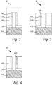
- Figure 2 is a plan view of a cross-section of Figure 1 of one fin 120 along the geometrical line AA' shown in the cut region 20 at a stage subsequent to formation of the fin cut mask 30.
- Figure 2 may be made to one fin 120, the following process steps may be performed in parallel on any further fins.
- the insulating layer 150 has been etched back in the fin cut region 20 to expose a portion of the capping layer 140 covering the upper surface of the fin 120.
- the insulating layer 150 may be etched back using any conventional oxide or dielectric wet or dry etch process allowing etching of the insulating layer 150.
- the exposed portion of the capping layer 140 has thereafter been opened to expose the upper surface of the fin 120.
- the exposed portion of the capping layer 140 may be removed in a wet or vapor etching process. For instance, a HCl-based etching process such as a HCI vapor etch may be used.
- the capping layer 140 may be opened by etching the capping layer material selectively to the fin material forming the upper surface of the fin 120.
- the fin 120 has been cut by etching the fin 120 in the cut region 20.
- the fin 120 has accordingly been cut or divided into a number of fin parts 122 remaining in the active regions 10.
- a perspective view subsequent to the fin cut and removal of the fin cut mask 30 is shown in Figure 5 .
- the fin parts 122 are separated by gaps formed in the cut regions 20.
- a selective etching approach has been used such that the capping layer 140 covering sidewalls of the semiconductor fin 120 is preserved. It should however be noted that the removal of the capping layers 140 and the fins 120 may also be performed in a single etching step i.e.
- the fin 120 may be etched using wet or vapor etching, for instance HCI-vapor etch.
- the presence of the capping layer 140 on the fin parts 122 may ensure that the fin parts 122 form strained fin parts 122.
- the fin cut depth corresponds to the height of the fin 120. I.e. the cut extends completely through the fin 120.
- the material of the insulating layer 150 has the ability to withstand the etching processes during the fin cutting, it is possible to remove the fin cut mask 130 subsequent to opening the insulating layer 150 in the cut regions 20.
- the capped fin 120 may thereafter be cut by etching in the cut regions 20, via the openings in the insulating layer 150, while the insulating layer 150 masks the capped fin 120 in the active regions 10.
- the fin cut mask 30 may be used to define the active regions 10 and the cut regions 20 but need not be used as an etch mask during the fin cutting.
- the fin cut mask 30 may be defined to cover the capped fin in the active regions 10 and expose the capped fin in the cut regions 20, and thereafter be used as an etch mask during the fin cutting.
- Figure 6 shows a plan view of a cross-section of the fin 120 along line A-A' wherein the gap in the cut region 20 has been refilled with a fill structure 160 of an insulating material.
- the fill structure 160 may be formed of a dielectric material such as SiO 2 , Si 3 N 4 , HfO 2 , ZrO 2 . These dielectric materials may be deposited using a CVD, physical vapor deposition (PVD), or atomic layer deposition (ALD) technique.
- PVD physical vapor deposition
- ALD atomic layer deposition
- the fill structure may subsequently be subjected to an anneal step such that the insulating material of the fill structure 160 may solidify. An anneal step may however be omitted if the fill structure 160 is in a solid state already after being deposited.
- the fill structure 160 may be deposited such that a height of the fill structure 160 may be the same as the height of the fin 120, or slightly below. Although in the illustrated process flow, the fin cut mask 30 has been removed prior to forming the fill structure 160, it is also possible to first form the fill structure 160 (and optionally perform the anneal) and thereafter remove the fin cut mask 30.
- the capping layer 140 may also be cut into a number of capping layer parts, each capping layer part formed on a respective fin part 122. The removal of the capping layer 140 may provide electrical insulation of the fin parts 122, for the purpose of subsequent device processing.
- Figure 8 shows a perspective view of the structure of figure 7 after removal of the insulating material 150. As shown in Figure 8 , the gaps in the cut region 20 is filled with the fill structure 160.
- Figures 9-14 show another method for cutting a semiconductor fin.
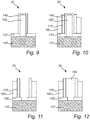
- Figure 9 shows a plan view of a cross-section of a fin 120 and a capping layer 140 within a cut region 20, however at a stage prior to forming the insulating layer 150 and the fin cut mask 30.
- a sidewall spacer 170 has been formed on and along sidewalls of the capped fin 120.
- the sidewall spacer 170 may be formed of an insulating material, for instance a nitride-based material such as Si 3 N 4 , an oxide-based material such as SiO 2 , or an hafnium-based material such as HfO 2 .
- the sidewall spacer 170 may be formed in a sidewall spacer deposition approach.
- a spacer layer may be conformally deposited, e.g. by ALD, to cover the capped fin(s) 120 and the insulating layer 130.
- Spacer layer portions deposited on horizontally oriented surfaces may subsequently be removed using a vertical anisotropic etch step, such that spacer layer portions deposited on vertically oriented surfaces may be preserved to form the sidewall spacer 170.
- the insulating layer 150 may be formed to embed the fin(s) 120 with the capping layer 140 and the sidewall spacer 170 formed thereon.
- the method may then proceed with fin cut mask formation and fin cutting as outlined above.
- the capping layer 140 may be removed in the cut region 20.
- a fill structure 160 may thereafter be formed in the cut region 20, between fin parts, as shown in figure 12 .
- the sidewall spacer 170 has been removed.
- the sidewall spacer 170 may be removed from an entire length of the fin 120.
- Figure 14 shows the resulting structure following removal of the insulating layer 150.
- Figures 15-18 show yet another method for cutting a semiconductor fin 120.
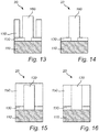
- Figures 15-17 illustrate cutting of a fin into a number of fin parts (fin parts 222, see Figure 18 ) by etching the fin in a cut region 20 without any preceding capping layer formation step.
- Figure 18 shows a perspective view subsequent to the fin cut process and after removal of the insulating material 150.
- a capping layer 140 has been formed on each fin part 222.
- the discussion of the capping layer 140 in connection with the above methods applies correspondingly to this method.
- the capping layer 140 shown in Figure 18 is formed also on the end surfaces of the fin parts 222, which are exposed in/face the cut regions during the capping layer 140 formation. The capping layer 140 may accordingly introduce strain into the fin parts 222.
Landscapes
- Insulated Gate Type Field-Effect Transistor (AREA)
- Thin Film Transistor (AREA)
Abstract
Description
- The present inventive concept relates to a method for cutting a semiconductor fin extending along a substrate. The present inventive concept further relates to a semiconductor structure.
- The ongoing trend for miniaturizing the dimensions of circuit elements and improving their functionalities requires continuous scaling of the feature size of the building blocks of the circuit elements. An example of such building blocks is a semiconductor fin, a three-dimensional (3D) body made of a semiconductor material. A common application for semiconductor fins include fin field effect transistors (FINFETs). Semiconductor fin fabrication may typically comprise patterning fins in one or more epitaxial semiconductor layers. The fins may be defined using single- or multiple patterning techniques such as self-aligned double patterning (SADP) or self-aligned quadruple patterning (SAQP). Each fin may be said to extend along a respective "fin track". The fins may subsequently be subjected to a fin cutting process, wherein transverse cuts or gaps are etched through the fins to form a number of fin parts along each fin track. Devices, such as FinFETs, may thereafter be formed along the fin parts.
- In some applications fins may be formed on a semiconductor substrate made of a material with a different lattice constant than the fins. The fins may hence be pre-strained due to the lattice mismatch between the fin and substrate in order to increase carrier mobility in the channel. However, applying a fin cut process to such a pre-strained fin may result in an at least partial relaxation of the lattice structure of the fin parts, especially in the regions of the cuts. This may in turn degrade the electrical properties of the devices to be formed on the fin parts.
- An objective of the present inventive concept is to address this issue. Further and alternative objectives may be understood from the following.
- According to an aspect of the present inventive concept there is provided a method for cutting a semiconductor fin extending along a substrate, the method comprising forming a fin cut mask, the fin cut mask defining a number of masked regions and a number of cut regions, and cutting the fin into a number of fin parts by etching the fin in said cut regions, wherein the method further comprises forming an epitaxial semiconductor capping layer on the fin prior to forming the fin cut mask or on the fin parts subsequent to cutting the fin, wherein a capping layer material and a fin material are lattice mismatched.
- According to a further aspect of the present inventive concept there is provided a semiconductor structure comprising a substrate, a number of semiconductor fin parts extending along the substrate, and an epitaxial semiconductor capping layer formed on each fin part, wherein a capping layer material and a fin material are lattice mismatched.
- The present inventive concept allows providing an interface between the fin or fin parts and the capping layer which forms a lattice-mismatched heterojunction. The substrate may be a semiconductor substrate providing a pre-strain to the fin. If the epitaxial semiconductor capping layer is formed on the fin prior to cutting the fin, the lattice-mismatch may counteract or limit relaxation of a pre-strained lattice structure of the fin after cutting the fin into a number of fin parts. If the capping layer is formed on the fin parts, subsequent to cutting the fin into a number of fin parts, the lattice-mismatch may recover a pre-strain in the fin parts. In addition, in both scenarios the epitaxial semiconductor capping layer on the fin or fin parts may also be used to apply additional strain to the lattice structure of the respective fin or fin parts.
- Although the inventive concept advantageously may be applied on a pre-strained fin, it is not limited thereto. Indeed, the capping layer may also be employed to provide strain in a fin, or in fin parts of a cut fin, exhibiting no pre-strain.
- The method may further comprise subsequent to cutting the fin, forming a fill structure by refilling gaps in said cut regions, between fin parts, with an insulating material. Thereby, the fill structure in the cut regions may maintain a separation between the fin parts. The fill structure may also provide mechanical support for the fin parts during further processing steps.
- The fill structure may be subjected to an anneal. Thereby the insulating material of the fill structure may solidify.
- The method may further comprise, prior to forming the fin cut mask, forming an insulating layer embedding a bottom portion of the fin, wherein forming the capping layer comprises forming the capping layer on an upper portion of the fin or fin parts protruding above the insulating layer. The insulating layer may mask the substrate during the formation of the capping layer and thus counteract capping layer deposition on the substrate (e.g. in regions between fin parts or between the fin and any further fins present on the substrate). The insulating layer may further form a shallow trench insulation (STI) and provide electrical insulation towards any neighboring fins present on the substrate.
- The method may further comprise, prior to cutting the fin, forming an insulating layer embedding the fin in the cut regions. Thereby, the insulating layer may be formed on opposite sides of fin in the cut region. The insulating layer may provide mechanical support for the capping layer during etching of the fin in the cut region.
- According to some embodiments, the epitaxial semiconductor capping layer may be formed on the fin prior to forming the fin cut mask, thereby forming a capped fin. The capped fin may accordingly comprise cutting the capped fin into a number of capped fin parts by etching the capped fin in said cut regions.
- The capping layer may cover sidewall surfaces of the fin. The capping layer may cover a top surface of the fin. The capping layer may accordingly form a cladding on the fin.
- During the etching of the fin, the fin cut mask may expose capping layer portions on top surface in the cut regions. Meanwhile, the fin cut mask may mask the capping layer and the fin in the mask regions. Exposed capping layer portions on the top surface may be removed from the fin during the cutting of the fin. The capping layer portions and the fin may be etched in a same etch step or in two or more sequential etch steps (e.g. a first etch step for etching the capping layer portions and a second etch step for etching the fin).
- The method may further comprise removing the capping layer in said cut regions during the cutting of the (capped) fin or subsequent to the cutting of the (capped) fin. Thereby, the capping layer in the cut region may be removed to provide electrical separation between the fin parts.
- The method may further comprise forming a fill structure by refilling gaps in said cut regions, between fin parts, with an insulating material, wherein the capping layer is removed in the cut regions subsequent to forming the fill structure. The presence of the fill structure may counteract relaxation when the capping layer is removed in the cut regions. In line with what was described above, the fill structure may further be subjected to an anneal.
- The method may further comprise, subsequent to forming the capping layer and prior to forming the fin cut mask, forming a sidewall spacer layer on capping layer portions formed along sidewalls of the fin. The sidewall spacer may provide structural support for the fin during the fin cutting. The sidewall spacer which may further facilitate simultaneous cutting/etching of the fin and the capping layer by counteracting relaxation, which otherwise could occur when the capping layer is etched in the cut regions.
- Subsequent to forming the sidewall spacer layer, an insulating layer may be formed to embed the fin with the capping layer and sidewall spacer layer formed thereon, and exposing an upper surface of the fin. Thereby, the insulating layer may be formed on opposite sides of the fin. The insulating layer may be formed along an entire length of the fin and to cover the fin. Thereby, the insulating layer may provide a planar surface on which the fin cut mask may be formed. The formation of the insulating layer may provide mechanical support for the sidewall spacer during etching of the fin and/or capping layer in the cut regions.
- The method may further comprise removing the sidewall spacer layer subsequent to cutting the fin. More specifically, the sidewall spacer layer may be removed subsequent to removing the fin cut mask.
- According to some embodiments, the epitaxial semiconductor capping layer may be formed on the fin parts subsequent to cutting the fin. Thereby the capping layer may form a cladding on the fin parts i.e. the capping layer may be formed on at least a top surface and sidewall surfaces of each fin part. The capping layer may also be formed on end surfaces of each fin part (i.e. the surfaces of the fin parts facing the cut regions). As may be understood from the above, the cladding may introduce and/or preserve strain within the fin parts.
- The semiconductor fin may be formed of a silicon (Si) and/or germanium (Ge) comprising material. The capping layer may be formed of a silicon and/or germanium material of a different composition than the semiconductor fin. The fin may more generally be formed of Si[y]Ge[1-y] and the capping layer may be formed of Si[x]Ge[1-x] where 0≤x≤1, 0≤y≤1 and x and y are different. The difference in x and y ratios allows the capping layer to introduce strain in the fin. In general, the capping layer composition may be similar to the substrate composition. For instance, for a p-type device, such as a pFET, the substrate may be a silicon substrate and the capping layer may be of silicon, i.e. consisting of silicon. For an n-type device, such as nFET, the substrate and the capping layer may be of silicon-germanium, for instance Si0.5Ge0.5.
- The above, as well as additional objects, features and advantages of the present inventive concept, will be better understood through the following illustrative and non-limiting detailed description, with reference to the appended drawings. In the drawings like reference numerals will be used for like elements unless stated otherwise.
-
Figures 1-18 schematically illustrate various methods for cutting a fin structure in to a number of fin parts. - Various methods for cutting a fin into a number of fin parts will now be disclosed in connection with
figures 1-18 . -
Figure 1 shows in perspective a sectional view of a region of asubstrate 110. InFigure 1 , the axis Z denotes a vertical direction, corresponding to a normal direction with respect to an upper surface of thesubstrate 110. The axis X denotes a first horizontal direction along thesubstrate 110 and the axis Y denotes a second horizontal direction along thesubstrate 110, perpendicular to the first direction X. It should be noted that in the drawings the relative dimensions of the shown elements, such as the height, width or thickness of elements, is merely schematic and may, for the purpose of illustrational clarity, differ from a physical structure. - A number of
semiconductor fins 120 extend along thesubstrate 110.Figure 1 shows twofins 120 however it should be noted that there may be any number of further fins outside the illustrated region. Eachfin 120 extends in parallel to the X axis. Eachfin 120 protrudes vertically above thesubstrate 110, i.e. in parallel to the Z axis. By way of example, a typical height of afin 120 above thesubstrate 110 may be in a range from 20 to 200 nm. A width of a fin 120 (i.e. along the Y axis) may be in a range from 3 to 30 nm for example. - The
substrate 110 may be anyconventional substrate 110, such as a substrate suitable for complementary metal-oxide semiconductor (CMOS) processing. Thesubstrate 110 may be a semiconductor substrate such as a Si substrate, a Ge substrate or a silicon-germanium (SiGe) substrate. Other examples include a silicon-on-insulator (SOI) substrate, a GeOI substrate or a SiGeOI substrate. - The
fins 120 may be formed of a silicon and/or germanium comprising material, i.e. of silicon-germanium (Si[y]Ge[1-y] and 0≤y≤1), depending on the intended application. Thefins 120 may also be multi-layered fins, e.g. formed of a stack of two or more silicon and/or germanium comprising material layers of different compositions. A multi-layered fin may for instance comprise a first layer of Si[yi]Ge[1-y1] with 0≤y1≤1 and a second layer of Si[y2]Ge[1-y2] with 0≤y2≤1 and y2≠y1, the second layer formed on the first layer. The first layer may form a "sacrificial" layer intended to be removed at a later stage of device processing, selectively to the second layer. The second layer may form a "channel" layer intended to allow formation of a transistor channel. The sacrificial layer may be removed selectively with respect to the channel layer, wherein the second layer may remain to allow formation of a gate structure completely wrapping around the "suspended" second layer. As per se is known in the art, fins may comprise a repetitive sequence of such first and second layers to allow formation of vertically stacked channel layers. - The fins 120 (or at least a bottom-layer thereof in case of multi-layered fins) may be formed of a material having a lattice constant different than the
substrate 110. Thereby, thefins 120 may be pre-strained due to a lattice mismatch at an interface between thefins 120 and the upper surface of thesubstrate 110. For instance, the upper surface of thesubstrate 110 may be formed by Si and thefins 120 may be formed of Si[y]Ge[1-y] and 0≤y<1, or vice versa. As will be further described below, acapping layer 140 may be formed on thefins 120 to counteract relaxation of pre-strained fins after a fin cut process. It is however also possible to form thefins 120 without any pre-strain, e.g. by forming thefins 120 of a material not presenting a lattice-mismatch with respect to the upper surface of thesubstrate 110. - The
fins 120 may be formed in a manner which per se is known in the art, e.g. by patterning thefins 120 in one or more epitaxial semiconductor layers by etching trenches in the semiconductor layer(s). The epitaxial semiconductor layer(s) may be formed in an epitaxial growth process on the upper surface of thesubstrate 110 using e.g. Chemical Vapor Deposition (CVD), metalorganic CVD (MOCVD), molecular beam epitaxy (MBE) or vapor phase epitaxy (VPE) techniques. If thesubstrate 110 comprises a semiconductor-on-insulator structure, thefins 120 may be patterned directly in the semiconductor layer of the structure. - Subsequent to forming the
fins 120, a bottom portion of thesemiconductor fin 120 may be embedded in an insulatinglayer 130. The insulatinglayer 130 may cover thesubstrate 110 in regions adjacent to and in between thefins 120. An insulating material, e.g. an oxide material such as silicon dioxide or a low-k dielectric material, may be deposited and etched back to define a layer of a desired thickness. The insulatinglayer 130 may for instance form a shallow-trench-insulation (STI), filling lower portions of trenches formed between fins during fin patterning. - The method proceeds by forming an
epitaxial capping layer 140 on thefins 120. Thecapping layer 140 covers a top surface and sidewall surfaces of eachfin 120. Thecapping layer 140 may accordingly form a cladding on eachfin 120. More specifically, thecapping layer 140 may be formed on surface portions of eachfin 120 exposed above the insulatinglayer 130. The capping layer material and a fin material are lattice mismatched with respect to each other such that an interface between eachfin 120 and thecapping layer 140 forms a lattice-mismatched heterojunction. For instance, in case of a Si- and/or Ge-comprising fins 120 (Si[y]Ge[1-y]) thecapping layer 140 may be formed of a different Si- and/or Ge-comprising material (e.g. Si[x]Ge[1-x] where 0≤x≤1 and x ≠ y). In case ofmulti-layered fins 120, the composition of thecapping layer 140 may advantageously be different from the composition of the sacrificial layer(s). - By way of example, on
fins 120 of Si[y]Ge[1-y] intended to support p-type device fabrication (e.g. p-type FETs) thecapping layer 140 may be formed of a material having a lower Ge-content than the fins. Conversely, onfins 120 intended to support n-type device fabrication (e.g. n-type FETs) thecapping layer 140 may be formed of a material having a greater Ge-content than the fins. In case ofmulti-layered fins 120 comprising two or more silicon and/or germanium comprising material layers of different compositions, the capping layer material may be different from at least one of the layers, e.g. at least each of the one or more second "channel" layers. - The lattice mismatch between the
capping layer 140 and eachfin 120 may induce strain in thefin 120. The strain may be compressive or tensile, depending on the degree of lattice mismatch. Parameters for thecapping layer 140 relevant for the strain-inducing function comprise the degree of lattice mismatch with respect to thefins 120 and a thickness of thecapping layer 140. Thecapping layer 140 may accordingly be formed with a composition and a thickness such that a desired amount of strain is induced in eachfin 120. In a case thefins 120 are pre-strained due to lattice mismatch between thefins 120 and thesubstrate 110, thecapping layer 140 may create additional strain in eachfin 120. - The
capping layer 140 may be formed in an epitaxial growth process. Due to the presence of the insulatinglayer 130, capping layer growth on the upper surface of thesubstrate 110 may be counteracted wherein thecapping layer 140 may be selectively deposited on the surface portions of eachfin 120 protruding above the insulatinglayer 130. - According to one example, for the case of non-pre-strained
fins 120 for a pFET device, thesubstrate 110 may be formed of Si0.7Ge0.3, thefins 120 may be 7 nm wide and be formed of Si0.7Ge0.3, and thecapping layer 140 may be 3 nm thick and be formed of Si material. According to another example, for the case of non-pre-strainedfins 120 for an nFET device, thesubstrate 110 may be formed of Si, thefins 120 may be 7 nm wide and be formed of Si, and thecapping layer 140 may be 3 nm thick and be formed of Si0.7Ge0.3 material. According to another example, for the case ofpre-strained fins 120 for a pFET device, thesubstrate 110 may be formed of Si, thefins 120 may be 7 nm wide and be formed of Si0.7Ge0.3, and thecapping layer 140 may be 3 nm thick and be formed of Si material. According to another example, for the case ofpre-strained fins 120 for an nFET device, thesubstrate 110 may be formed of Si0.7Ge0.3, thefins 120 may be may be 7 nm wide and be formed of Si, and thecapping layer 140 may be 3 nm thick and be formed of Si0.7Ge0.3 materials. It should be noted that these examples only are provided as illustrative examples and that other compositions and dimensions of the various elements also are possible. - Subsequent to forming the
capping layer 140, thefins 120 with thecapping layer 140 formed thereon may be embedded and covered in a further insulatinglayer 150. The insulatinglayer 150 may be formed using any of the techniques and any of the materials discussed in connection with the insulatinglayer 130. The method proceeds by forming afin cut mask 30 above thefins 120. The fin cutmask 30 defines a number of mask regions 10 (in which respective fin parts will remain following fin cutting) and a number of cut regions 20 (in which thefins 120 will be cut by etching). As the fin parts remaining in themask regions 10 may be used to define active devices, the mask regions may in the following be referred to asactive regions 10. The region illustrated inFigure 1 shows asingle cut region 20, however as would be appreciated by the skilled person a plurality of such cut regions may be defined along the length of eachfin 120. A length of thecut region 20, defining a separation between twoadjacent fin parts 122 may be in a range from 5 to 200 nm, depending on the intended application. - The fin cut
mask 30 may be a photoresist layer with lithographically definedactive regions 10 and cutregions 20. The fin cutmask 30 may also be a lithographic mask layer stack (a "litho stack"), comprising in a bottom-up-direction for instance a patterning layer (e.g. an organic or non-organic patterning film), one or more transfer layers (e.g. anti-reflective coatings such as SiOC layers or spin-on-glass layers, and a planarization layer such as a spin-on-carbon layer), and a photoresist layer. As per se is known in the art, a pattern may be lithographically defined in the photoresist layer and subsequently transferred into lower layers of the litho stack, in a number of etch steps, and subsequently into the patterning layer. The pattern may thereafter be transferred from the patterning layer into the underlying layers, e.g. the insulatinglayer 150 and thefins 120, as will be described below. -
Figure 2 is a plan view of a cross-section ofFigure 1 of onefin 120 along the geometrical line AA' shown in thecut region 20 at a stage subsequent to formation of the fin cutmask 30. Although, reference in the following may be made to onefin 120, the following process steps may be performed in parallel on any further fins. - In
Figure 3 , the insulatinglayer 150 has been etched back in the fin cutregion 20 to expose a portion of thecapping layer 140 covering the upper surface of thefin 120. The insulatinglayer 150 may be etched back using any conventional oxide or dielectric wet or dry etch process allowing etching of the insulatinglayer 150. The exposed portion of thecapping layer 140 has thereafter been opened to expose the upper surface of thefin 120. The exposed portion of thecapping layer 140 may be removed in a wet or vapor etching process. For instance, a HCl-based etching process such as a HCI vapor etch may be used. Thecapping layer 140 may be opened by etching the capping layer material selectively to the fin material forming the upper surface of thefin 120. - In
Figure 4 , thefin 120 has been cut by etching thefin 120 in thecut region 20. Thefin 120 has accordingly been cut or divided into a number offin parts 122 remaining in theactive regions 10. A perspective view subsequent to the fin cut and removal of the fin cutmask 30 is shown inFigure 5 . As shown, thefin parts 122 are separated by gaps formed in thecut regions 20. In the illustrated case, a selective etching approach has been used such that thecapping layer 140 covering sidewalls of thesemiconductor fin 120 is preserved. It should however be noted that the removal of the capping layers 140 and thefins 120 may also be performed in a single etching step i.e. simultaneous etching of thefin 120 and thecapping layer 140, provided the materials of thecapping layer 140 and thefin 120 are not too dissimilar. Thefin 120 may be etched using wet or vapor etching, for instance HCI-vapor etch. In any case, as described above, the presence of thecapping layer 140 on thefin parts 122 may ensure that thefin parts 122 form strainedfin parts 122. In the illustrated case, the fin cut depth corresponds to the height of thefin 120. I.e. the cut extends completely through thefin 120. However, it is also possible to cut the fin by etching partially through the height of thefin 120. For improved fin-to-fin isolation it may however be advantageous to extend the etching even into the underlying substrate, i.e. thereby forming cuts being deeper than the original fin height. - According to a variation, provided the material of the insulating
layer 150 has the ability to withstand the etching processes during the fin cutting, it is possible to remove the fin cutmask 130 subsequent to opening the insulatinglayer 150 in thecut regions 20. The cappedfin 120 may thereafter be cut by etching in thecut regions 20, via the openings in the insulatinglayer 150, while the insulatinglayer 150 masks the cappedfin 120 in theactive regions 10. Accordingly, the fin cutmask 30 may be used to define theactive regions 10 and thecut regions 20 but need not be used as an etch mask during the fin cutting. - It should be noted that it is also possible to etch back the insulating
layer 150 to make the upper surface thereof flush with the upper surface of the capped fin, prior to forming the fin cutmask 30. Accordingly, the fin cutmask 30 may be defined to cover the capped fin in theactive regions 10 and expose the capped fin in thecut regions 20, and thereafter be used as an etch mask during the fin cutting. -
Figure 6 shows a plan view of a cross-section of thefin 120 along line A-A' wherein the gap in thecut region 20 has been refilled with afill structure 160 of an insulating material. Thefill structure 160 may be formed of a dielectric material such as SiO2, Si3N4, HfO2, ZrO2. These dielectric materials may be deposited using a CVD, physical vapor deposition (PVD), or atomic layer deposition (ALD) technique. The fill structure may subsequently be subjected to an anneal step such that the insulating material of thefill structure 160 may solidify. An anneal step may however be omitted if thefill structure 160 is in a solid state already after being deposited. Thefill structure 160 may be deposited such that a height of thefill structure 160 may be the same as the height of thefin 120, or slightly below. Although in the illustrated process flow, the fin cutmask 30 has been removed prior to forming thefill structure 160, it is also possible to first form the fill structure 160 (and optionally perform the anneal) and thereafter remove the fin cutmask 30. - With reference to
Figure 7 , subsequent to forming thefill structure 160, portions of thecapping layer 140 extending through thecut region 10 have been removed by etching. Accordingly, thecapping layer 140 may also be cut into a number of capping layer parts, each capping layer part formed on arespective fin part 122. The removal of thecapping layer 140 may provide electrical insulation of thefin parts 122, for the purpose of subsequent device processing. -
Figure 8 shows a perspective view of the structure offigure 7 after removal of the insulatingmaterial 150. As shown inFigure 8 , the gaps in thecut region 20 is filled with thefill structure 160. -
Figures 9-14 show another method for cutting a semiconductor fin.Figure 9 shows a plan view of a cross-section of afin 120 and acapping layer 140 within acut region 20, however at a stage prior to forming the insulatinglayer 150 and the fin cutmask 30. - In
Figure 10 asidewall spacer 170 has been formed on and along sidewalls of the cappedfin 120. Thesidewall spacer 170 may be formed of an insulating material, for instance a nitride-based material such as Si3N4, an oxide-based material such as SiO2, or an hafnium-based material such as HfO2. Thesidewall spacer 170 may be formed in a sidewall spacer deposition approach. A spacer layer may be conformally deposited, e.g. by ALD, to cover the capped fin(s) 120 and the insulatinglayer 130. Spacer layer portions deposited on horizontally oriented surfaces may subsequently be removed using a vertical anisotropic etch step, such that spacer layer portions deposited on vertically oriented surfaces may be preserved to form thesidewall spacer 170. Subsequent to forming thesidewall spacer 170, the insulatinglayer 150 may be formed to embed the fin(s) 120 with thecapping layer 140 and thesidewall spacer 170 formed thereon. - With reference to
Figure 11 , the method may then proceed with fin cut mask formation and fin cutting as outlined above. As further discussed above, also thecapping layer 140 may be removed in thecut region 20. - A
fill structure 160 may thereafter be formed in thecut region 20, between fin parts, as shown infigure 12 . InFigure 13 thesidewall spacer 170 has been removed. Thesidewall spacer 170 may be removed from an entire length of thefin 120.Figure 14 shows the resulting structure following removal of the insulatinglayer 150. -
Figures 15-18 show yet another method for cutting asemiconductor fin 120.Figures 15-17 illustrate cutting of a fin into a number of fin parts (fin parts 222, seeFigure 18 ) by etching the fin in acut region 20 without any preceding capping layer formation step. -
Figure 18 shows a perspective view subsequent to the fin cut process and after removal of the insulatingmaterial 150. Acapping layer 140 has been formed on eachfin part 222. The discussion of thecapping layer 140 in connection with the above methods applies correspondingly to this method. However, in contrast to the above, thecapping layer 140 shown inFigure 18 is formed also on the end surfaces of thefin parts 222, which are exposed in/face the cut regions during thecapping layer 140 formation. Thecapping layer 140 may accordingly introduce strain into thefin parts 222. - In the above the inventive concept has mainly been described with reference to a limited number of examples. However, as is readily appreciated by a person skilled in the art, other examples than the ones disclosed above are equally possible within the scope of the inventive concept, as defined by the appended claims.
Claims (15)
- A method for cutting a semiconductor fin (120) extending along a substrate (110), the method comprising:forming a fin cut mask (30), the fin cut mask (30) defining a number of masked regions (10) and a number of cut regions (20), andcutting the fin (120) into a number of fin parts (122) by etching the fin (120) in said cut regions (20),wherein the method further comprises forming an epitaxial semiconductor capping layer (140) on the fin (120) prior to forming the fin cut mask (30) or on the fin parts (122) subsequent to cutting the fin (120), wherein a capping layer material and a fin material are lattice mismatched.
- A method according to claim 1, further comprising subsequent to cutting the fin (120), forming a fill structure (160) by refilling gaps in said cut regions (20), between fin parts (122), with an insulating material.
- A method according to claim 2, further comprising subjecting the fill structure (160) to an anneal.
- A method according to any preceding claim, further comprising, prior to forming the fin cut mask (30), forming an insulating layer (130) embedding a bottom portion of the fin (120), wherein forming the capping layer (140) comprises forming the capping layer (140) on an upper portion of the fin (120) or the fin parts (122) protruding above the insulating layer (130).
- A method according to any preceding claim, wherein the epitaxial semiconductor capping layer (140) is formed on the fin (120) prior to forming the fin cut mask (30).
- A method according to claim 5, further comprising removing the capping layer (140) in said cut regions (20) during the cutting of the fin (120) or subsequent to the cutting of the fin (120).
- A method according to claim 6, further comprising, forming a fill structure (160) by refilling gaps in said cut regions (20), between fin parts (122), with an insulating material, wherein the capping layer is removed subsequent to forming the fill structure (160).
- A method according to any of claims 5-7, further comprising, subsequent to forming the capping layer (140) and prior to forming the fin cut mask (30), forming a sidewall spacer layer (170) on capping layer portions (140) formed along sidewalls of the fin (120).
- A method according to claim 8, further comprising, subsequent to forming the sidewall spacer layer (170), forming an insulating layer (150) embedding the fin (120) with the capping layer (140) and sidewall spacer layer (170) formed thereon.
- A method according to claim 8-9, further comprising, removing the sidewall spacer layer (170) subsequent to cutting the fin (120).
- A method according to any of claims 1-4, wherein the epitaxial semiconductor capping layer (140) is formed on the fin parts (122) subsequent to cutting the fin (120).
- A method according to any of the preceding claims, wherein the capping layer (140) is an epitaxial silicon layer or an epitaxial germanium layer.
- A method according to any of the preceding claims, wherein semiconductor fin (120) is formed of a silicon and/or germanium comprising material.
- A method according to any of the preceding claims, wherein the substrate (110) is a semiconductor substrate providing a pre-strain to the fin (120).
- A semiconductor structure comprising:a substrate (110), a number of semiconductor fin parts (122) extending along the substrate, andan epitaxial semiconductor capping layer (140) formed on each fin part (122), wherein a capping layer material and a fin material are lattice mismatched.
Priority Applications (2)
| Application Number | Priority Date | Filing Date | Title |
|---|---|---|---|
| EP18248027.7A EP3675159B1 (en) | 2018-12-27 | 2018-12-27 | A semiconductor structure and a method for cutting a semiconductor fin |
| US16/719,852 US11387350B2 (en) | 2018-12-27 | 2019-12-18 | Semiconductor fin structure and method of fabricating the same |
Applications Claiming Priority (1)
| Application Number | Priority Date | Filing Date | Title |
|---|---|---|---|
| EP18248027.7A EP3675159B1 (en) | 2018-12-27 | 2018-12-27 | A semiconductor structure and a method for cutting a semiconductor fin |
Publications (2)
| Publication Number | Publication Date |
|---|---|
| EP3675159A1 true EP3675159A1 (en) | 2020-07-01 |
| EP3675159B1 EP3675159B1 (en) | 2023-05-24 |
Family
ID=65019281
Family Applications (1)
| Application Number | Title | Priority Date | Filing Date |
|---|---|---|---|
| EP18248027.7A Active EP3675159B1 (en) | 2018-12-27 | 2018-12-27 | A semiconductor structure and a method for cutting a semiconductor fin |
Country Status (2)
| Country | Link |
|---|---|
| US (1) | US11387350B2 (en) |
| EP (1) | EP3675159B1 (en) |
Citations (4)
| Publication number | Priority date | Publication date | Assignee | Title |
|---|---|---|---|---|
| US20050202604A1 (en) * | 2003-02-13 | 2005-09-15 | Zhiyuan Cheng | Integrated semiconductor device and method to make same |
| US20140027816A1 (en) * | 2012-07-27 | 2014-01-30 | Stephen M. Cea | High mobility strained channels for fin-based transistors |
| US20160351590A1 (en) * | 2015-05-27 | 2016-12-01 | International Business Machines Corporation | Preventing strained fin relaxation |
| US20180166570A1 (en) * | 2016-12-12 | 2018-06-14 | Applied Materials, Inc. | Method of forming conformal epitaxial semiconductor cladding material over a fin field effect transistor (finfet) device |
Family Cites Families (10)
| Publication number | Priority date | Publication date | Assignee | Title |
|---|---|---|---|---|
| US8658536B1 (en) | 2012-09-05 | 2014-02-25 | Globalfoundries Inc. | Selective fin cut process |
| US8617996B1 (en) | 2013-01-10 | 2013-12-31 | Globalfoundries Inc. | Fin removal method |
| US9147730B2 (en) | 2014-03-03 | 2015-09-29 | Globalfoundries Inc. | Methods of forming fins for FinFET semiconductor devices and selectively removing some of the fins by performing a cyclical fin cutting process |
| US9704973B2 (en) | 2014-04-01 | 2017-07-11 | Globalfoundries Inc. | Methods of forming fins for FinFET semiconductor devices and the selective removal of such fins |
| US9406680B1 (en) * | 2015-02-13 | 2016-08-02 | Taiwan Semiconductor Manufacturing Co., Ltd. | Semiconductor device including fin structures and manufacturing method thereof |
| US10615255B2 (en) | 2016-02-12 | 2020-04-07 | International Business Machines Corporation | Fin formation for semiconductor device |
| US10483169B2 (en) | 2016-09-29 | 2019-11-19 | Taiwan Semiconductor Manufacturing Company, Ltd. | FinFET cut-last process using oxide trench fill |
| US10128239B2 (en) * | 2016-10-17 | 2018-11-13 | International Business Machines Corporation | Preserving channel strain in fin cuts |
| US10867859B2 (en) * | 2017-11-17 | 2020-12-15 | Taiwan Semiconductor Manufacturing Co., Ltd. | Methods of fabricating semiconductor devices having isolation structures with liners |
| US10600695B2 (en) * | 2018-05-22 | 2020-03-24 | International Business Machines Corporation | Channel strain formation in vertical transport FETS with dummy stressor materials |
-
2018
- 2018-12-27 EP EP18248027.7A patent/EP3675159B1/en active Active
-
2019
- 2019-12-18 US US16/719,852 patent/US11387350B2/en active Active
Patent Citations (4)
| Publication number | Priority date | Publication date | Assignee | Title |
|---|---|---|---|---|
| US20050202604A1 (en) * | 2003-02-13 | 2005-09-15 | Zhiyuan Cheng | Integrated semiconductor device and method to make same |
| US20140027816A1 (en) * | 2012-07-27 | 2014-01-30 | Stephen M. Cea | High mobility strained channels for fin-based transistors |
| US20160351590A1 (en) * | 2015-05-27 | 2016-12-01 | International Business Machines Corporation | Preventing strained fin relaxation |
| US20180166570A1 (en) * | 2016-12-12 | 2018-06-14 | Applied Materials, Inc. | Method of forming conformal epitaxial semiconductor cladding material over a fin field effect transistor (finfet) device |
Also Published As
| Publication number | Publication date |
|---|---|
| US20200212205A1 (en) | 2020-07-02 |
| EP3675159B1 (en) | 2023-05-24 |
| US11387350B2 (en) | 2022-07-12 |
Similar Documents
| Publication | Publication Date | Title |
|---|---|---|
| US12027607B2 (en) | Methods for GAA I/O formation by selective epi regrowth | |
| CN114121807B (en) | Method for forming a transistor structure | |
| US9373704B2 (en) | Multiple-gate semiconductor device and method | |
| TWI419324B (en) | Semiconductor device having three-five-group channel and four-group source drain and manufacturing method thereof | |
| TWI592983B (en) | Method of forming a III-V channel | |
| US9954104B2 (en) | Multiwidth finFET with channel cladding | |
| US9142673B2 (en) | Devices and methods of forming bulk FinFETS with lateral seg for source and drain on dielectrics | |
| US11107812B2 (en) | Method of fabricating stacked semiconductor device | |
| US10615278B2 (en) | Preventing strained fin relaxation | |
| US12484289B2 (en) | Method for forming a stacked transistor device | |
| US11521902B2 (en) | Vertical field-effect transistor (VFET) devices and methods of forming the same | |
| US20150123211A1 (en) | NARROW DIFFUSION BREAK FOR A FIN FIELD EFFECT (FinFET) TRANSISTOR DEVICE | |
| US12520556B2 (en) | Method for forming a semiconductor device | |
| CN105870061B (en) | The method and apparatus of dual resisteance in strained silicon-on-insulator wafers | |
| US11088263B2 (en) | Method of forming vertical field effect transistor device | |
| US11387350B2 (en) | Semiconductor fin structure and method of fabricating the same | |
| US20230197525A1 (en) | Method for Forming a Semiconductor Device Structure | |
| US20200357701A1 (en) | Vertical field-effect transistor (vfet) devices and methods of forming the same | |
| US20250212440A1 (en) | Method for forming a semiconductor structure | |
| US20250212494A1 (en) | Method for Forming a Semiconductor Structure | |
| KR102589730B1 (en) | Field Effect Transistor and Method of fabricating the same |
Legal Events
| Date | Code | Title | Description |
|---|---|---|---|
| PUAI | Public reference made under article 153(3) epc to a published international application that has entered the european phase |
Free format text: ORIGINAL CODE: 0009012 |
|
| STAA | Information on the status of an ep patent application or granted ep patent |
Free format text: STATUS: THE APPLICATION HAS BEEN PUBLISHED |
|
| AK | Designated contracting states |
Kind code of ref document: A1 Designated state(s): AL AT BE BG CH CY CZ DE DK EE ES FI FR GB GR HR HU IE IS IT LI LT LU LV MC MK MT NL NO PL PT RO RS SE SI SK SM TR |
|
| AX | Request for extension of the european patent |
Extension state: BA ME |
|
| STAA | Information on the status of an ep patent application or granted ep patent |
Free format text: STATUS: REQUEST FOR EXAMINATION WAS MADE |
|
| 17P | Request for examination filed |
Effective date: 20201209 |
|
| RBV | Designated contracting states (corrected) |
Designated state(s): AL AT BE BG CH CY CZ DE DK EE ES FI FR GB GR HR HU IE IS IT LI LT LU LV MC MK MT NL NO PL PT RO RS SE SI SK SM TR |
|
| GRAP | Despatch of communication of intention to grant a patent |
Free format text: ORIGINAL CODE: EPIDOSNIGR1 |
|
| STAA | Information on the status of an ep patent application or granted ep patent |
Free format text: STATUS: GRANT OF PATENT IS INTENDED |
|
| INTG | Intention to grant announced |
Effective date: 20221213 |
|
| GRAS | Grant fee paid |
Free format text: ORIGINAL CODE: EPIDOSNIGR3 |
|
| GRAA | (expected) grant |
Free format text: ORIGINAL CODE: 0009210 |
|
| STAA | Information on the status of an ep patent application or granted ep patent |
Free format text: STATUS: THE PATENT HAS BEEN GRANTED |
|
| AK | Designated contracting states |
Kind code of ref document: B1 Designated state(s): AL AT BE BG CH CY CZ DE DK EE ES FI FR GB GR HR HU IE IS IT LI LT LU LV MC MK MT NL NO PL PT RO RS SE SI SK SM TR |
|
| REG | Reference to a national code |
Ref country code: GB Ref legal event code: FG4D |
|
| REG | Reference to a national code |
Ref country code: CH Ref legal event code: EP |
|
| REG | Reference to a national code |
Ref country code: DE Ref legal event code: R096 Ref document number: 602018050143 Country of ref document: DE |
|
| REG | Reference to a national code |
Ref country code: AT Ref legal event code: REF Ref document number: 1570085 Country of ref document: AT Kind code of ref document: T Effective date: 20230615 |
|
| P01 | Opt-out of the competence of the unified patent court (upc) registered |
Effective date: 20230513 |
|
| REG | Reference to a national code |
Ref country code: IE Ref legal event code: FG4D |
|
| REG | Reference to a national code |
Ref country code: LT Ref legal event code: MG9D |
|
| REG | Reference to a national code |
Ref country code: NL Ref legal event code: MP Effective date: 20230524 |
|
| REG | Reference to a national code |
Ref country code: AT Ref legal event code: MK05 Ref document number: 1570085 Country of ref document: AT Kind code of ref document: T Effective date: 20230524 |
|
| PG25 | Lapsed in a contracting state [announced via postgrant information from national office to epo] |
Ref country code: SE Free format text: LAPSE BECAUSE OF FAILURE TO SUBMIT A TRANSLATION OF THE DESCRIPTION OR TO PAY THE FEE WITHIN THE PRESCRIBED TIME-LIMIT Effective date: 20230524 Ref country code: PT Free format text: LAPSE BECAUSE OF FAILURE TO SUBMIT A TRANSLATION OF THE DESCRIPTION OR TO PAY THE FEE WITHIN THE PRESCRIBED TIME-LIMIT Effective date: 20230925 Ref country code: NO Free format text: LAPSE BECAUSE OF FAILURE TO SUBMIT A TRANSLATION OF THE DESCRIPTION OR TO PAY THE FEE WITHIN THE PRESCRIBED TIME-LIMIT Effective date: 20230824 Ref country code: NL Free format text: LAPSE BECAUSE OF FAILURE TO SUBMIT A TRANSLATION OF THE DESCRIPTION OR TO PAY THE FEE WITHIN THE PRESCRIBED TIME-LIMIT Effective date: 20230524 Ref country code: ES Free format text: LAPSE BECAUSE OF FAILURE TO SUBMIT A TRANSLATION OF THE DESCRIPTION OR TO PAY THE FEE WITHIN THE PRESCRIBED TIME-LIMIT Effective date: 20230524 Ref country code: AT Free format text: LAPSE BECAUSE OF FAILURE TO SUBMIT A TRANSLATION OF THE DESCRIPTION OR TO PAY THE FEE WITHIN THE PRESCRIBED TIME-LIMIT Effective date: 20230524 |
|
| PG25 | Lapsed in a contracting state [announced via postgrant information from national office to epo] |
Ref country code: RS Free format text: LAPSE BECAUSE OF FAILURE TO SUBMIT A TRANSLATION OF THE DESCRIPTION OR TO PAY THE FEE WITHIN THE PRESCRIBED TIME-LIMIT Effective date: 20230524 Ref country code: PL Free format text: LAPSE BECAUSE OF FAILURE TO SUBMIT A TRANSLATION OF THE DESCRIPTION OR TO PAY THE FEE WITHIN THE PRESCRIBED TIME-LIMIT Effective date: 20230524 Ref country code: LV Free format text: LAPSE BECAUSE OF FAILURE TO SUBMIT A TRANSLATION OF THE DESCRIPTION OR TO PAY THE FEE WITHIN THE PRESCRIBED TIME-LIMIT Effective date: 20230524 Ref country code: LT Free format text: LAPSE BECAUSE OF FAILURE TO SUBMIT A TRANSLATION OF THE DESCRIPTION OR TO PAY THE FEE WITHIN THE PRESCRIBED TIME-LIMIT Effective date: 20230524 Ref country code: IS Free format text: LAPSE BECAUSE OF FAILURE TO SUBMIT A TRANSLATION OF THE DESCRIPTION OR TO PAY THE FEE WITHIN THE PRESCRIBED TIME-LIMIT Effective date: 20230924 Ref country code: HR Free format text: LAPSE BECAUSE OF FAILURE TO SUBMIT A TRANSLATION OF THE DESCRIPTION OR TO PAY THE FEE WITHIN THE PRESCRIBED TIME-LIMIT Effective date: 20230524 Ref country code: GR Free format text: LAPSE BECAUSE OF FAILURE TO SUBMIT A TRANSLATION OF THE DESCRIPTION OR TO PAY THE FEE WITHIN THE PRESCRIBED TIME-LIMIT Effective date: 20230825 |
|
| PG25 | Lapsed in a contracting state [announced via postgrant information from national office to epo] |
Ref country code: FI Free format text: LAPSE BECAUSE OF FAILURE TO SUBMIT A TRANSLATION OF THE DESCRIPTION OR TO PAY THE FEE WITHIN THE PRESCRIBED TIME-LIMIT Effective date: 20230524 |
|
| PG25 | Lapsed in a contracting state [announced via postgrant information from national office to epo] |
Ref country code: SK Free format text: LAPSE BECAUSE OF FAILURE TO SUBMIT A TRANSLATION OF THE DESCRIPTION OR TO PAY THE FEE WITHIN THE PRESCRIBED TIME-LIMIT Effective date: 20230524 |
|
| PG25 | Lapsed in a contracting state [announced via postgrant information from national office to epo] |
Ref country code: SM Free format text: LAPSE BECAUSE OF FAILURE TO SUBMIT A TRANSLATION OF THE DESCRIPTION OR TO PAY THE FEE WITHIN THE PRESCRIBED TIME-LIMIT Effective date: 20230524 Ref country code: SK Free format text: LAPSE BECAUSE OF FAILURE TO SUBMIT A TRANSLATION OF THE DESCRIPTION OR TO PAY THE FEE WITHIN THE PRESCRIBED TIME-LIMIT Effective date: 20230524 Ref country code: RO Free format text: LAPSE BECAUSE OF FAILURE TO SUBMIT A TRANSLATION OF THE DESCRIPTION OR TO PAY THE FEE WITHIN THE PRESCRIBED TIME-LIMIT Effective date: 20230524 Ref country code: EE Free format text: LAPSE BECAUSE OF FAILURE TO SUBMIT A TRANSLATION OF THE DESCRIPTION OR TO PAY THE FEE WITHIN THE PRESCRIBED TIME-LIMIT Effective date: 20230524 Ref country code: DK Free format text: LAPSE BECAUSE OF FAILURE TO SUBMIT A TRANSLATION OF THE DESCRIPTION OR TO PAY THE FEE WITHIN THE PRESCRIBED TIME-LIMIT Effective date: 20230524 Ref country code: CZ Free format text: LAPSE BECAUSE OF FAILURE TO SUBMIT A TRANSLATION OF THE DESCRIPTION OR TO PAY THE FEE WITHIN THE PRESCRIBED TIME-LIMIT Effective date: 20230524 |
|
| REG | Reference to a national code |
Ref country code: DE Ref legal event code: R097 Ref document number: 602018050143 Country of ref document: DE |
|
| PLBE | No opposition filed within time limit |
Free format text: ORIGINAL CODE: 0009261 |
|
| STAA | Information on the status of an ep patent application or granted ep patent |
Free format text: STATUS: NO OPPOSITION FILED WITHIN TIME LIMIT |
|
| 26N | No opposition filed |
Effective date: 20240227 |
|
| PG25 | Lapsed in a contracting state [announced via postgrant information from national office to epo] |
Ref country code: SI Free format text: LAPSE BECAUSE OF FAILURE TO SUBMIT A TRANSLATION OF THE DESCRIPTION OR TO PAY THE FEE WITHIN THE PRESCRIBED TIME-LIMIT Effective date: 20230524 |
|
| PG25 | Lapsed in a contracting state [announced via postgrant information from national office to epo] |
Ref country code: SI Free format text: LAPSE BECAUSE OF FAILURE TO SUBMIT A TRANSLATION OF THE DESCRIPTION OR TO PAY THE FEE WITHIN THE PRESCRIBED TIME-LIMIT Effective date: 20230524 Ref country code: IT Free format text: LAPSE BECAUSE OF FAILURE TO SUBMIT A TRANSLATION OF THE DESCRIPTION OR TO PAY THE FEE WITHIN THE PRESCRIBED TIME-LIMIT Effective date: 20230524 |
|
| REG | Reference to a national code |
Ref country code: CH Ref legal event code: PL |
|
| PG25 | Lapsed in a contracting state [announced via postgrant information from national office to epo] |
Ref country code: LU Free format text: LAPSE BECAUSE OF NON-PAYMENT OF DUE FEES Effective date: 20231227 |
|
| PG25 | Lapsed in a contracting state [announced via postgrant information from national office to epo] |
Ref country code: MC Free format text: LAPSE BECAUSE OF FAILURE TO SUBMIT A TRANSLATION OF THE DESCRIPTION OR TO PAY THE FEE WITHIN THE PRESCRIBED TIME-LIMIT Effective date: 20230524 |
|
| GBPC | Gb: european patent ceased through non-payment of renewal fee |
Effective date: 20231227 |
|
| REG | Reference to a national code |
Ref country code: BE Ref legal event code: MM Effective date: 20231231 |
|
| PG25 | Lapsed in a contracting state [announced via postgrant information from national office to epo] |
Ref country code: MC Free format text: LAPSE BECAUSE OF FAILURE TO SUBMIT A TRANSLATION OF THE DESCRIPTION OR TO PAY THE FEE WITHIN THE PRESCRIBED TIME-LIMIT Effective date: 20230524 Ref country code: LU Free format text: LAPSE BECAUSE OF NON-PAYMENT OF DUE FEES Effective date: 20231227 |
|
| REG | Reference to a national code |
Ref country code: IE Ref legal event code: MM4A |
|
| PG25 | Lapsed in a contracting state [announced via postgrant information from national office to epo] |
Ref country code: IE Free format text: LAPSE BECAUSE OF NON-PAYMENT OF DUE FEES Effective date: 20231227 |
|
| PG25 | Lapsed in a contracting state [announced via postgrant information from national office to epo] |
Ref country code: GB Free format text: LAPSE BECAUSE OF NON-PAYMENT OF DUE FEES Effective date: 20231227 |
|
| PG25 | Lapsed in a contracting state [announced via postgrant information from national office to epo] |
Ref country code: BE Free format text: LAPSE BECAUSE OF NON-PAYMENT OF DUE FEES Effective date: 20231231 |
|
| PG25 | Lapsed in a contracting state [announced via postgrant information from national office to epo] |
Ref country code: FR Free format text: LAPSE BECAUSE OF NON-PAYMENT OF DUE FEES Effective date: 20231231 |
|
| PG25 | Lapsed in a contracting state [announced via postgrant information from national office to epo] |
Ref country code: CH Free format text: LAPSE BECAUSE OF NON-PAYMENT OF DUE FEES Effective date: 20231231 |
|
| PG25 | Lapsed in a contracting state [announced via postgrant information from national office to epo] |
Ref country code: IE Free format text: LAPSE BECAUSE OF NON-PAYMENT OF DUE FEES Effective date: 20231227 Ref country code: GB Free format text: LAPSE BECAUSE OF NON-PAYMENT OF DUE FEES Effective date: 20231227 Ref country code: FR Free format text: LAPSE BECAUSE OF NON-PAYMENT OF DUE FEES Effective date: 20231231 Ref country code: CH Free format text: LAPSE BECAUSE OF NON-PAYMENT OF DUE FEES Effective date: 20231231 Ref country code: BE Free format text: LAPSE BECAUSE OF NON-PAYMENT OF DUE FEES Effective date: 20231231 |
|
| PG25 | Lapsed in a contracting state [announced via postgrant information from national office to epo] |
Ref country code: BG Free format text: LAPSE BECAUSE OF FAILURE TO SUBMIT A TRANSLATION OF THE DESCRIPTION OR TO PAY THE FEE WITHIN THE PRESCRIBED TIME-LIMIT Effective date: 20230524 |
|
| REG | Reference to a national code |
Ref country code: DE Ref legal event code: R079 Ref document number: 602018050143 Country of ref document: DE Free format text: PREVIOUS MAIN CLASS: H01L0021823400 Ipc: H10D0084830000 |
|
| PG25 | Lapsed in a contracting state [announced via postgrant information from national office to epo] |
Ref country code: BG Free format text: LAPSE BECAUSE OF FAILURE TO SUBMIT A TRANSLATION OF THE DESCRIPTION OR TO PAY THE FEE WITHIN THE PRESCRIBED TIME-LIMIT Effective date: 20230524 |
|
| PG25 | Lapsed in a contracting state [announced via postgrant information from national office to epo] |
Ref country code: CY Free format text: LAPSE BECAUSE OF FAILURE TO SUBMIT A TRANSLATION OF THE DESCRIPTION OR TO PAY THE FEE WITHIN THE PRESCRIBED TIME-LIMIT; INVALID AB INITIO Effective date: 20181227 |
|
| PG25 | Lapsed in a contracting state [announced via postgrant information from national office to epo] |
Ref country code: HU Free format text: LAPSE BECAUSE OF FAILURE TO SUBMIT A TRANSLATION OF THE DESCRIPTION OR TO PAY THE FEE WITHIN THE PRESCRIBED TIME-LIMIT; INVALID AB INITIO Effective date: 20181227 |
|
| PG25 | Lapsed in a contracting state [announced via postgrant information from national office to epo] |
Ref country code: TR Free format text: LAPSE BECAUSE OF FAILURE TO SUBMIT A TRANSLATION OF THE DESCRIPTION OR TO PAY THE FEE WITHIN THE PRESCRIBED TIME-LIMIT Effective date: 20230524 |
|
| PGFP | Annual fee paid to national office [announced via postgrant information from national office to epo] |
Ref country code: DE Payment date: 20251126 Year of fee payment: 8 |