EP3674969A1 - Method and apparatus for recognizing fingerprint logo, and electronic device - Google Patents
Method and apparatus for recognizing fingerprint logo, and electronic device Download PDFInfo
- Publication number
- EP3674969A1 EP3674969A1 EP18921287.1A EP18921287A EP3674969A1 EP 3674969 A1 EP3674969 A1 EP 3674969A1 EP 18921287 A EP18921287 A EP 18921287A EP 3674969 A1 EP3674969 A1 EP 3674969A1
- Authority
- EP
- European Patent Office
- Prior art keywords
- region
- fingerprint
- sub
- regions
- image
- Prior art date
- Legal status (The legal status is an assumption and is not a legal conclusion. Google has not performed a legal analysis and makes no representation as to the accuracy of the status listed.)
- Granted
Links
Images



Classifications
-
- G—PHYSICS
- G06—COMPUTING OR CALCULATING; COUNTING
- G06V—IMAGE OR VIDEO RECOGNITION OR UNDERSTANDING
- G06V40/00—Recognition of biometric, human-related or animal-related patterns in image or video data
- G06V40/10—Human or animal bodies, e.g. vehicle occupants or pedestrians; Body parts, e.g. hands
- G06V40/12—Fingerprints or palmprints
- G06V40/1365—Matching; Classification
-
- G—PHYSICS
- G06—COMPUTING OR CALCULATING; COUNTING
- G06V—IMAGE OR VIDEO RECOGNITION OR UNDERSTANDING
- G06V40/00—Recognition of biometric, human-related or animal-related patterns in image or video data
- G06V40/10—Human or animal bodies, e.g. vehicle occupants or pedestrians; Body parts, e.g. hands
- G06V40/12—Fingerprints or palmprints
- G06V40/1347—Preprocessing; Feature extraction
- G06V40/1353—Extracting features related to minutiae or pores
-
- G—PHYSICS
- G06—COMPUTING OR CALCULATING; COUNTING
- G06V—IMAGE OR VIDEO RECOGNITION OR UNDERSTANDING
- G06V40/00—Recognition of biometric, human-related or animal-related patterns in image or video data
- G06V40/10—Human or animal bodies, e.g. vehicle occupants or pedestrians; Body parts, e.g. hands
- G06V40/12—Fingerprints or palmprints
- G06V40/13—Sensors therefor
- G06V40/1324—Sensors therefor by using geometrical optics, e.g. using prisms
-
- G—PHYSICS
- G06—COMPUTING OR CALCULATING; COUNTING
- G06V—IMAGE OR VIDEO RECOGNITION OR UNDERSTANDING
- G06V40/00—Recognition of biometric, human-related or animal-related patterns in image or video data
- G06V40/10—Human or animal bodies, e.g. vehicle occupants or pedestrians; Body parts, e.g. hands
- G06V40/12—Fingerprints or palmprints
- G06V40/13—Sensors therefor
- G06V40/1318—Sensors therefor using electro-optical elements or layers, e.g. electroluminescent sensing
-
- G—PHYSICS
- G06—COMPUTING OR CALCULATING; COUNTING
- G06V—IMAGE OR VIDEO RECOGNITION OR UNDERSTANDING
- G06V40/00—Recognition of biometric, human-related or animal-related patterns in image or video data
- G06V40/60—Static or dynamic means for assisting the user to position a body part for biometric acquisition
- G06V40/63—Static or dynamic means for assisting the user to position a body part for biometric acquisition by static guides
Definitions
- the present disclosure relates to the field of fingerprint identification, and more particularly, to a method and apparatus for identifying a fingerprint logo and an electronic device.
- under-screen optical fingerprint identification technology under a screen of a liquid crystal display (Liquid Crystal Display, LCD) and an organic light-emitting diode (Organic Light-Emitting Diode, OLED) display.
- LCD Liquid Crystal Display
- OLED Organic Light-Emitting Diode
- a part to be pressed is prompted on a display screen, and mainly includes two patterns: one is a fingerprint logo prompting a user to perform pressing, and the other is a pattern of a captured fingerprint image. If an optical fingerprint image contains logo information, false rejection rate (False Rejection Rate, FRR) of fingerprint identification will be greatly affected.
- FRR False Rejection Rate
- the present disclosure provides a method and apparatus for identifying a fingerprint logo and an electronic device.
- an image of a local region may be firstly captured to determine whether there is a fingerprint logo currently, thereby solving a problem that a fingerprint logo is contained in a fingerprint image, reducing a risk of false fingerprint identification, and meanwhile, reducing FRR and False Acceptance Rate (False Acceptance Rate, FAR).
- a method for identifying a fingerprint logo including:
- fingerprint image capturing is only performed after a fingerprint logo is determined to disappear.
- a first image may be acquired by the optical sensor, and whether there is a fingerprint logo for guiding a user to perform pressing is identified in the first image, and then fingerprint image capturing is performed after the fingerprint logo is determined to disappear, thereby solving a problem that a fingerprint logo is contained in a fingerprint image, reducing a risk of false fingerprint identification, and meanwhile, reducing FRR and FAR, and improving user experience.
- the at least one first region corresponds to the partial region of the photosensitive surface of the optical sensor, that is, fingerprint logo identification may thus be implemented only through an image formed by an optical signal captured by an optical sensor in a local region, thereby improving user usage experience.
- the identifying whether there is the fingerprint logo for guiding the user to perform pressing in the first image according to the first optical signals captured in the at least one first region includes:
- fingerprint logo identification can be implemented through a relationship between light intensity information of at least one first region and a first threshold.
- the light intensity information is at least one of optical signal mean, optical signal standard deviation, optical signal variance, and optical signal weight ratio.
- the method before determining the light intensity information of the at least one first region respectively, the method further includes: performing consistency and/or binarization processing on the first optical signals captured in the at least one first region.
- the method further includes: configuring the first threshold.
- the method further includes:
- each of sub-regions corresponds to a plurality of pixel points, and each of the pixel points captures a first optical signal, that is, first optical signals are captured in each of the sub-regions.
- fingerprint logo identification is performed between different sub-regions in each of at least one first region, and it can be confirmed that there is the fingerprint logo in the first image as long as the fingerprint logo is identified in any first region.
- fingerprint identification can be implemented through difference information between different sub-regions in the first region.
- the determining the difference information between the different sub-regions of the plurality of sub-regions according to the first optical signals of each of the sub-regions includes:
- the light intensity information is at least one of optical signal mean, optical signal standard deviation, optical signal variance, and optical signal weight ratio.
- the method before determining the light intensity information of each of the sub-regions, the method further includes: performing consistency and/or binarization processing on the first optical signals captured in the plurality of sub-regions.
- the light intensity information is optical signal weight ratio, assuming that there are sub-region 1 and sub-region 2, it needs to calculate weight of mean of an optical signal of the sub-region 1 greater than that of an optical signal of the sub-region 2.
- the light intensity information is optical signal variance, assuming that there is a sub-region 1, it needs to calculate variance of an optical signal of the sub-region 1.
- the plurality of sub-regions have different locations and/or shapes.
- the fingerprint logo includes at least one type of fingerprint logo.
- At least one type of fingerprint logo can be identified, that is, fingerprint logos of different electronic devices may be compatible, and fingerprint logos of different models of the same electronic device may be compatible, and actual fingerprint logo types of different models may be adjusted to improve user experience.
- the method further includes: determining the at least one first region according to location information of the fingerprint logo and current type of the fingerprint logo.
- the at least one first region can be determined.
- the method further includes: controlling the optical sensor to capture a fingerprint image.
- the method further includes:
- fingerprint logo disappearing time can be accurately determined, thereby avoiding a fingerprint logo contained in a captured fingerprint image, reducing a risk of false fingerprint identification, and meanwhile, reducing FRR.
- the method for identifying the fingerprint logo may be performed by a micro control unit (Micro Control Unit, MCU) in a fingerprint module including an optical sensor.
- MCU Micro Control Unit
- the MCU may control the optical sensor to capture an optical signal (an image)
- the MCU includes a memory for storing programs and data and a processor for calling and running the programs and the data stored in the memory, and the MCU is configured to perform the method in the first aspect or any of the possible implementation manners of the first aspect.
- the memory included in the above MCU may be a register, and the register may store some related algorithms for calculating mean, variance, standard deviation, and weight ratio, and may also store some algorithms for selection of a first region location, and may also store some parameter configuration information; and the processor in the above MCU calls related information in the register to perform the method in the first aspect or any of the possible implementation manners of the first aspect.
- the method for identifying the fingerprint logo may also be executed by a processor in an electronic device, for example, the processor executes the method in the first aspect or any of the possible implementation manners of the first aspect by some software running on the electronic device.
- the method for identifying the fingerprint logo may be the method in the first aspect or any of the possible implementation manners of the first aspect that is commonly executed by an MCU and a processor.
- an apparatus for identifying a fingerprint logo including:
- the processing unit is configured to:
- the processing unit before the processing unit determines the light intensity information of the at least one first region respectively, the processing unit is further configured to: perform consistency and/or binarization processing on the first optical signals captured in the at least one first region.
- the light intensity information is at least one of optical signal mean, optical signal standard deviation, optical signal variance, and optical signal weight ratio.
- the processing unit is further configured to configure the first threshold.
- the processing unit is further configured to divide each first region into a plurality of sub-regions, where each of the sub-regions corresponds to a plurality of pixel points of the optical sensor;
- the processing unit is configured to:
- the processing unit before the processing unit determines the light intensity information of each of the sub-regions, the processing unit is further configured to perform consistency and/or binarization processing on the first optical signals captured in the plurality of sub-regions.
- the light intensity information is at least one of optical signal mean, optical signal standard deviation, optical signal variance, and optical signal weight ratio.
- the plurality of sub-regions have different locations and/or shapes.
- the fingerprint logo includes at least one type of fingerprint logo.
- the processing unit is further configured to: determine the at least one first region according to location information of the fingerprint logo and current type of the fingerprint logo.
- the processing unit is further configured to control the optical sensor to capture a fingerprint image.
- the acquiring unit is further configured to acquire second optical signals captured by the optical sensor in the at least one first region respectively, where the second optical signals captured in the at least one first region form a second image; and the processing unit is further configured to identify whether there is the fingerprint logo in the second image according to the second optical signals captured in the at least one first region.
- the processing unit is a micro control unit (MCU) in a fingerprint module or a processor in an electronic device, where the fingerprint module includes the optical sensor.
- MCU micro control unit
- an electronic device including:
- a chip where the chip includes an input/output interface, at least one processor, at least one memory and a bus.
- the at least one memory is configured to store an instruction.
- the at least one processor is configured to call the instruction in the at least one memory, to execute the method in the first aspect or any of the possible implementation manners of the first aspect.
- an electronic device including the chip in the fourth aspect.
- a computer storage medium having stored therein program codes, the program codes being operative to indicate execution of the method in the above first aspect or any of the possible implementation manners in the first aspect.
- a computer program product including instructions which cause a computer to execute the method in the above first aspect or any of the possible implementation manners in the first aspect when run on the computer.
- a first image may be acquired by the optical sensor, and whether there is a fingerprint logo for guiding a user to perform pressing is identified in the first image, and then fingerprint image capturing is performed after the fingerprint logo is determined to disappear, thereby solving a problem that a fingerprint logo is contained in a fingerprint image, reducing a risk of false fingerprint identification, and meanwhile, reducing FRR and FAR.
- a solution of identifying a fingerprint logo greatly improves response speed and system reliability, and improves user experience.
- under-display or under-screen Under-display or Under-screen fingerprint identification technology
- the under-screen fingerprint identification technology refers to mounting a fingerprint identification module (such as a fingerprint identification module) under a display screen, so as to realize a fingerprint identification operation in a display region of the display screen without setting a fingerprint capturing region in a region other than the display region on the front of an electronic device.
- Optical under-screen fingerprint identification technology uses light returned from a top surface of a display component of a device for fingerprint sensing and other sensing operations.
- the returned light carries information of an object (e.g., a finger) in contact with the top surface, and by capturing and detecting the returned light, a particular optical sensor module under a display screen is implemented.
- the optical sensor module may be designed to achieve desired optical imaging by properly configuring optical elements for capturing and detecting the returned light.
- FIG. 1 and FIG. 2 are schematic views showing an electronic device 100 to which a fingerprint identification apparatus according to an embodiment of the present disclosure is applicable.
- FIG. 1 is a schematic front view of an electronic device 100
- FIG. 2 is a partial schematic cross-sectional structural view of the electronic device 100 shown in FIG. 1 taken along A-A'.
- the electronic device 100 includes a display screen 120 and an optical fingerprint identification apparatus (hereinafter referred to as a fingerprint identification apparatus in short) 130.
- the optical fingerprint identification apparatus 130 has one or more sensing arrays, and the sensing array(s) is/are disposed at least in a local region under the display screen 120 such that a fingerprint capturing region (or a sensing region) 103 of the optical fingerprint identification apparatus 130 is at least partially located in a display region 102 of the display screen 120.
- an area of the fingerprint capturing region 103 may be different from an area of the sensing array of the optical fingerprint identification apparatus 130.
- the area of the fingerprint capturing region 103 of the optical fingerprint identification apparatus 130 may be greater than the area of the sensing array of the optical fingerprint identification apparatus 130 through a lens imaging light path design, a reflective folding light path design or other light path designs such as light convergence or reflection.
- the area of the fingerprint capturing region 103 of the optical fingerprint identification apparatus 130 may also be designed to be substantially identical with the area of the sensing array of the optical fingerprint identification apparatus 130.
- the fingerprint capturing region 103 is located in the display region 102 of the display screen 120, and thus when a user needs to unlock or perform fingerprint verification on the electronic device, fingerprint input can be implemented as long as a finger is pressed on the fingerprint capturing region 103 located in the display screen 120. Since fingerprint detection can be implemented inside the screen, a front surface of the electronic device 100 in the foregoing structure does not need to specifically reserve a space to set a fingerprint button (such as a Home button), so that a full screen solution can be adopted, that is, the display region 102 of the display screen 120 can be substantially extended to the entire front surface of the electronic device 100.
- a fingerprint button such as a Home button
- the display screen 120 may be a self-emitting display screen, which adopts a self-emitting display unit as a display pixel, such as an organic light-emitting diode (Organic Light-Emitting Diode, OLED) display screen or a micro light-emitting diode (Micro-LED) display screen.
- OLED Organic Light-Emitting Diode
- Micro-LED micro light-emitting diode
- the optical fingerprint identification apparatus 130 may utilize an OLED display unit (that is, an OLED light source) of the OLED display screen 120 that is located in the fingerprint identifying region 103 as an excitation light source for optical fingerprint detection.
- the optical fingerprint identification apparatus 130 may also use an internal light source or an external light source to provide an optical signal for fingerprint detection.
- the optical fingerprint identification apparatus 130 may be applied to a non-self-emitting display screen, such as a liquid crystal display screen or other passive light-emitting display screens.
- a non-self-emitting display screen such as a liquid crystal display screen or other passive light-emitting display screens.
- an optical fingerprint system of the electronic device 100 may further include an excitation light source for optical fingerprint detection.
- the excitation light source may be specifically an infrared light source or a light source of non-visible light of a specific wavelength, which may be disposed under the backlight module of the liquid crystal display screen or disposed in an edge region under a protective cover of the electronic device 100.
- the optical fingerprint identification apparatus 130 may be disposed under the edge region of the liquid crystal panel or the protective cover, so that light for fingerprint detection can reach the optical fingerprint identification apparatus 130 by optical path directing.
- the optical fingerprint identification apparatus 130 may also be disposed under the backlight module, and the backlight module allows light for fingerprint detection to pass through the liquid crystal panel and the backlight module and reach the optical fingerprint identification apparatus 130 by providing a via hole or performing other optical designs on film layers such as a diffusion sheet, a brightening sheet, a reflection sheet, or the like.
- the sensing array of the optical fingerprint identification apparatus 130 may be specifically a photo detector (photo detector) array including a plurality of photo detectors arranged in an array, and the photo detectors may serve as optical sensing units as described above.
- a finger touches, presses, or approaches collectively referred to as touch in the present disclosure for convenience of description
- the fingerprint identifying region 103 When a finger touches, presses, or approaches (collectively referred to as touch in the present disclosure for convenience of description) the fingerprint identifying region 103, light emitted by a display unit of the fingerprint identifying region 103 is reflected by a fingerprint on a finger surface to form reflected light, where reflected light of a ridge of the fingerprint of the finger is different from that of a valley of the fingerprint of the finger, and the reflected light from the display screen 120 is received by the photo detector array and converted into a corresponding electrical signal, that is, a fingerprint detection signal.
- Fingerprint image data can be obtained based on the fingerprint detection signal, and fingerprint matching verification can be further performed,
- the electronic device 100 may further include a transparent protective cover 110, and the cover 110 may specifically be a transparent cover, such as a glass cover or a sapphire cover, which is located on the display screen 120 and covers the front surface of the electronic device 100. Therefore, in the embodiment of the present disclosure, the so-called finger touching, pressing or approaching the display screen 120 may actually refer to the finger touching, pressing or approaching the cover 110 on the display screen 120 or a protective layer covering a surface of the cover 110.
- the electronic device 100 may further include a touch sensor, and the touch sensor may specifically be a touch panel, which may be disposed on a surface of the display screen 120 or may be partially or entirely integrated into an interior of the display screen 120, that is, the display screen 120 is specifically a touch control display screen.
- the touch sensor may specifically be a touch panel, which may be disposed on a surface of the display screen 120 or may be partially or entirely integrated into an interior of the display screen 120, that is, the display screen 120 is specifically a touch control display screen.
- the optical fingerprint identification apparatus 130 includes an optical detection unit 134 and an optical component 132.
- the optical detection unit 134 includes the sensing array, and a readout circuit electrically connected to the sensing array as well as other auxiliary circuits, and may be fabricated on a die (Die) by a semiconductor process. That is, the optical detection unit 134 may be fabricated on an optical imaging chip, an image sensing chip or an optical sensor chip.
- the optical component 132 may be disposed above the sensing array of the optical detection unit 134, and may specifically include a filter (Filter), a light path directing structure, and other optical elements.
- the filter may be used to filter ambient light passing through a finger, and the light path directing structure is mainly used to direct a light path such as collimating, modulating or converging light that propagates downward, thereby implementing directing of the reflected light reflected from the finger surface to the sensing array for optical detection.
- a light path such as collimating, modulating or converging light that propagates downward, thereby implementing directing of the reflected light reflected from the finger surface to the sensing array for optical detection.
- the optical component 132 may be encapsulated in the same optical fingerprint chip with the optical detection unit 134, or the optical component 132 may be disposed outside a chip where the optical detection unit 134 is located, for example the optical component 132 is attached above the chip, or some elements of the optical component 132 are integrated into the chip.
- the light path directing structure of the optical component 132 for example, a light path modulator or a light path collimator fabricated on a semiconductor silicon wafer or other substrates, and the light path modulator or the light path collimator has a plurality of light path modulating units or collimating units, which may be specifically micro-hole arrays.
- a light directing layer may also be an optical lens (Lens) layer having one or more lens units, such as a lens group consisting of one or more aspherical lenses. After optically collimated or converged by the micro-hole arrays or the lens units, a reflected light reflected from a finger is received by the optical sensing units underneath, so that the sensing array may detect a fingerprint image of the finger.
- Lens optical lens
- a circuit board 140 may further be provided under the optical fingerprint identification apparatus 130.
- the optical fingerprint identification apparatus 130 may be soldered to the circuit board 140 through a pad for example, and achieves electrical interconnection and signal transmission with other peripheral circuits or other elements of the electronic device 100 through the circuit board 140.
- the optical fingerprint identification apparatus 130 may receive a control signal of a processing unit of the electronic device 100 through the circuit board 140, and may also output the fingerprint detection signal to the processing unit, a control unit or the like of the electronic device 100 through the circuit board 140.
- the display screen 120 may prompt a part to be pressed, mainly including two patterns: one is a fingerprint logo prompting a user to perform pressing, and the other is a pattern of a captured fingerprint image. If an optical fingerprint image contains logo information, FRR of fingerprint identification will be greatly affected. The presence of the fingerprint logo in the fingerprint image is due to the fact that the fingerprint logo does not completely disappear during an exposure process.
- a method for eliminating a logo in a fingerprint image in an optical fingerprint is mainly to perform a fixed delay on a host side, and issue a fingerprint image capturing command after the fingerprint logo is completely eliminated.
- the above method is a fixed delay method, a time point of fingerprint logo elimination cannot be accurately known, so user experience is reduced.
- an embodiment of the present disclosure provides an improved technical solution. Specifically, a method for identifying a fingerprint logo is provided. Before starting to capture a fingerprint image normally, an image of a local region may be firstly captured to determine whether there is a fingerprint logo currently, thereby solving a problem of a fingerprint logo contained in a fingerprint image, reducing a risk of fingerprint identification, and meanwhile, reducing FRR.
- FIG. 3 is a schematic flowchart of a method 200 for identifying a fingerprint logo according to an embodiment of the present disclosure. As shown in FIG. 3 , the method 200 includes:
- the method 200 may be executed by an electronic device.
- the method 200 may be executed by a processor (such as a central processing unit (Central Processing Unit, CPU)) in the electronic device.
- the processor executes the method 200 through some software running on the electronic device.
- the method 200 may further be executed by a fingerprint identification module including at least one optical sensor.
- the method 200 may be executed by an MCU in the fingerprint identification module.
- the MCU may control the optical sensor to capture an optical signal (an image), and the MCU includes a memory for storing programs and data and a processor for calling and running the programs and the data stored in the memory, and the MCU is configured to execute the method 200.
- the memory included in the above MCU may be a register, and the register may store some related algorithms for calculating mean, variance, standard deviation, and weight ratio, and may also store some algorithms for selection of a first region location, and may also store some parameter configuration information.
- the above MCU may be integrated, for example, on an image processing chip, which may be used to optimize the optical sensor to capture an image.
- the optical sensor in the embodiment of the present disclosure may correspond to the optical detection unit 134 in the optical fingerprint identification apparatus 130 in FIG. 1 , and the method 200 may be applied to an optical fingerprint identification apparatus including a plurality of optical sensors, so as to achieve a large area of fingerprint identification.
- the at least one first region corresponds to the partial region of the photosensitive surface of the optical sensor, that is, fingerprint logo identification may thus be implemented only through an image formed by an optical signal captured by an optical sensor in a local region, thereby improving user usage experience.
- a first image may be acquired by an optical sensor, and whether there is a fingerprint logo for guiding a user to perform pressing is identified in the first image, and then fingerprint image capturing is performed after the fingerprint logo is determined to disappear, thereby solving a problem that a fingerprint logo is contained in a fingerprint image, reducing a risk of false fingerprint identification, and meanwhile, reducing FRR.
- the first optical signals may bear fingerprint information or may not bear fingerprint information. That is, the first image may carry fingerprint information or may not carry fingerprint information.
- the MCU may identify whether there is at least one type of fingerprint logo in the first image.
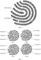
- the MCU may identify whether there are four different types of fingerprint logos as shown in FIG. 4 in the first image.
- the method for identifying the fingerprint logo in the embodiment of the present disclosure may be compatible with fingerprint logos of different electronic devices, and may also be compatible with fingerprint logos of different models of the same electronic device, and may be adjusted based on an actual type of fingerprint logo of a different model, thereby improving user experience.
- the MCU may determine the at least one first region according to location information of the fingerprint logo and current type of the fingerprint logo.
- the MCU can easily know the location information of the fingerprint logo and the current type of the fingerprint logo.
- the MCU can determine the at least one first region.
- the MCU may identify whether there is the fingerprint logo for guiding the user to perform pressing in the first image from the level of the first region according to the first optical signals captured in the at least one first region.
- the MCU determines light intensity information of the at least one first region respectively according to the first optical signals captured in the at least one first region. Further, if there is light intensity information greater than a first threshold in the light intensity information of the at least one first region, the MCU determines that there is the fingerprint logo in the first image; or if there is not light intensity information greater than a first threshold in the light intensity information of the at least one first region, the MCU determines that there is not the fingerprint logo in the first image.
- the MCU determines that there is the fingerprint logo in the first image.
- the MCU determines the light intensity information of the at least one first region respectively.
- the MCU performs consistency and/or binarization processing on the first optical signals captured in the at least one first region.
- the first image can be optimized, thereby making it easier to identify whether there is the fingerprint logo in the first image.
- the light intensity information is at least one of optical signal mean, optical signal standard deviation, optical signal variance, and optical signal weight ratio.
- optical signal mean of the first region 1 is A
- optical signal mean of the first region 2 is B
- mean of all first optical signals captured in the first region 1 is thus solved as A
- mean of all first optical signals captured in the first region 2 is thus solved as B.
- optical signal standard deviation of the first region 1 is C
- optical signal standard deviation of the first region 2 is D
- standard deviation of all first optical signals captured in the first region 1 is thus solved as C
- standard deviation of all first optical signals captured in the first region 2 is thus solved as D.
- optical signal variance of the first region 1 is E, and optical signal variance of the first region 2 is F; and variance of all first optical signals captured in the first region 1 is thus solved as E, and variance of all first optical signals captured in the first region 2 is thus solved as F.
- optical signal weight ratio of the first region 1 is X
- optical signal weight ratio of the first region 2 is Y
- mean of all first optical signals captured in the first region 1 is A, and ratio of an optical signal of which mean is greater than A in all first optical signals captured in the first region 1 is thus X
- mean of all first optical signals captured in the first region 2 is B, and ratio of an optical signal of which mean is greater than B in all first optical signals captured in the first region 2 is thus Y.
- a graphic presented by a shadow is a fingerprint logo.
- the MCU may configure the first threshold.
- different first thresholds may be configured for different information included in the light intensity information.
- different first thresholds may be configured for different types of fingerprint logos.
- fingerprint logo identification can be implemented through a relationship between light intensity information of at least one first region and a first threshold.
- the MCU may identify whether there is the fingerprint logo for guiding the user to perform pressing in the first image from the level of the first region based on the first optical signals captured in the at least one first region.
- the MCU divides each first region into a plurality of sub-regions, and each of the sub-regions corresponds to a plurality of pixel points of the optical sensor. Further, the MCU determines difference information between different sub-regions of the plurality of sub-regions according to the first optical signals of each of the sub-regions, and identifies whether there is the fingerprint logo in the first image according to the difference information between the different sub-regions of the plurality of sub-regions.
- each of the sub-regions corresponds to a plurality of pixel points, and each of the pixel points captures a first optical signal, that is, first optical signals are captured in each of the sub-regions.
- the MCU may determine difference information between different sub-regions in the plurality of sub-regions by the following manners.
- the MCU determines light intensity information of each of the sub-regions according to the first optical signals of each of the sub-regions, and determines the difference information between the different sub-regions of the plurality of sub-regions according to the light intensity information of each of the sub-regions.
- the MCU may identify whether there is the fingerprint logo in the first image through the difference information between the different sub-regions in the first region. Certainly, fingerprint logo identification is performed in each of the at least one first region, and it can be confirmed that there is a fingerprint logo in the first image as long as the fingerprint logo is identified in any first region.
- the MCU may further perform consistency and/or binarization processing on the first optical signals captured in the plurality of sub-regions.
- the first image can be optimized, thereby making it easier to identify whether there is the fingerprint logo in the first image.
- the light intensity information is at least one of optical signal mean, optical signal standard deviation, optical signal variance, and optical signal weight ratio.
- the first region is divided into a sub-region 1 and a sub-region 2.
- optical signal mean of the sub-region 1 is A
- optical signal mean of the sub-region 2 is B
- mean of all first optical signals captured in the sub-region 1 is thus solved as A
- mean of all first optical signals captured in the sub-region 2 is thus solved as B.
- optical signal standard deviation of the sub-region 1 is C
- optical signal standard deviation of the sub-region 2 is D
- standard deviation of all first optical signals captured in the sub-region 1 is thus solved as C
- standard deviation of all first optical signals captured in the sub-region 2 is thus solved as D.
- optical signal variance of the sub-region 1 is E
- optical signal variance of the sub-region 2 is F
- variance of all first optical signals captured in the sub-region 1 is thus solved as E
- variance of all first optical signals captured in the sub-region 2 is thus solved as F.
- optical signal weight ratio of the sub-region 1 is X
- optical signal weight ratio of the sub-region 2 is Y
- mean of all first optical signals captured in the sub-region 1 is A
- mean of all first optical signals captured in the sub-region 2 is B
- ratio of an optical signal of which mean is greater than B in all first optical signals captured in the sub-region 1 is thus X
- ratio of an optical signal of which mean is greater than A in all first optical signals captured in the sub-region 2 is thus Y.
- a graphic presented by a shadow is a fingerprint logo.
- the plurality of sub-regions have different locations and/or shapes.
- the first region may be divided into a sub-region 1, a sub-region 2, and a sub-region 3, and the sub-region 1, the sub-region 2, and the sub-region 3 have four different shapes.
- the first region may be divided into a sub-region 1, a sub-region 2, and a sub-region 3, and the sub-region 1, the sub-region 2, and the sub-region 3 have four different locations.
- the MCU controls the optical sensor to capture a fingerprint image.
- the MCU acquires second optical signals captured by the optical sensor in the at least one first region respectively, where the second optical signals captured in the at least one first region form a second image; and the MCU identifies whether there is the fingerprint logo in the second image according to the second optical signals captured in the at least one first region.
- the MCU needs to re-execute related operations such as image capturing and fingerprint logo identification until the fingerprint logo disappears.
- the at least one first region may be re-determined, and the second optical signals are captured respectively based on the re-determined at least one first region.
- fingerprint logo disappearing time can be accurately determined, thereby avoiding a fingerprint logo contained in a captured fingerprint image, reducing a risk of false fingerprint identification, and meanwhile, reducing FRR.
- a weight analysis method can clearly distinguish fingerprint data with a fingerprint logo and fingerprint data without a fingerprint logo.
- the light intensity information is optical signal weight ratio
- a weight analysis method can clearly distinguish fingerprint data with a fingerprint logo and fingerprint data without a fingerprint logo.
- FIG. 9 in a first region, 78 pixel points are included, optical signals captured thereby are respectively identified as 1-78, and weight ratio analysis is performed on the optical signals captured by the 78 pixel points respectively. It can be seen that weight ratio of fingerprint data with a fingerprint logo is almost maintained at 100, while weight ratio of fingerprint data without a fingerprint logo is largely fluctuated, and the weight ratio is maintained in a range of 0-70.
- FIG. 10 is a schematic block diagram of an apparatus 300 for identifying a fingerprint logo according to an embodiment of the present disclosure. As shown in FIG. 10 , the apparatus 300 for identifying the fingerprint logo includes:
- the processing unit 320 is configured to:
- the processing unit 320 before the processing unit 320 determines the light intensity information of the at least one first region respectively, the processing unit 320 is further configured to: perform consistency and/or binarization processing on the first optical signals captured in the at least one first region.
- the light intensity information is at least one of optical signal mean, optical signal standard deviation, optical signal variance, and optical signal weight ratio.
- the processing unit 320 is further configured to configure the first threshold.
- the processing unit 320 is further configured to divide each first region into a plurality of sub-regions, where each of the sub-regions corresponds to a plurality of pixel points of the optical sensor; and the processing unit 320 is configured to: determine difference information between different sub-regions of the plurality of sub-regions according to the first optical signals of each of the sub-regions; and identify whether there is the fingerprint logo in the first image according to the difference information between the different sub-regions of the plurality of sub-regions.
- the processing unit 320 is configured to:
- the processing unit 320 before the processing unit 320 determines the light intensity information of each of the sub-regions, the processing unit 320 is further configured to perform consistency and/or binarization processing on the first optical signals captured in the plurality of sub-regions.
- the light intensity information is at least one of optical signal mean, optical signal standard deviation, optical signal variance, and optical signal weight ratio.
- the plurality of sub-regions have different locations and/or shapes.
- the fingerprint logo includes at least one type of fingerprint logo.
- the processing unit 320 is further configured to: determine the at least one first region according to location information of the fingerprint logo and current type of the fingerprint logo.
- the processing unit is further configured to control the optical sensor to capture a fingerprint image.
- the acquiring unit 310 is further configured to acquire second optical signals captured by the optical sensor in the at least one first region respectively, where the second optical signals captured in the at least one first region form a second image; and the processing unit 320 is further configured to identify whether there is the fingerprint logo in the second image according to the second optical signals captured in the at least one first region.
- the processing unit 320 is a micro control unit (MCU) in a fingerprint module or a processor in an electronic device, where the fingerprint module includes an optical sensor.
- MCU micro control unit
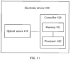
- FIG. 11 is a schematic block diagram of an electronic device 400 according to an embodiment of the present disclosure. As shown in FIG. 11 , the electronic device 400 includes:
- the processor of the embodiment of the present disclosure may be an integrated circuit chip with signal processing capability.
- steps of the foregoing method embodiments may be completed by using an integrated logical circuit of hardware in the processor or an instruction in a form of software.
- the processor may be a general purpose processor, a digital signal processor (Digital Signal Processor, DSP), an application-specific integrated circuit (Application Specific Integrated Circuit, ASIC), a field programmable gate array (Field Programmable Gate Array, FPGA) or another programmable logic device, a discrete gate or transistor logic device, or a discrete hardware component.
- DSP Digital Signal Processor
- ASIC Application Specific Integrated Circuit
- FPGA Field Programmable Gate Array
- the methods, the steps, and the logical block diagrams disclosed in the embodiments of the present disclosure can be implemented or executed.
- the general purpose processor may be a microprocessor or the processor may be any conventional processor or the like. Steps of the methods disclosed in the embodiments of the present disclosure may be directly executed and completed by using a hardware decoding processor, or may be executed and completed by using a combination of hardware and software modules in the decoding processor.
- the software module may be located in a mature storage medium in the art, such as a random access memory, a flash memory, a read-only memory, a programmable read-only memory, an electrically-erasable programmable memory, or a register.
- the storage medium is located in the memory, and the processor reads information in the memory and completes the steps of the foregoing method in combination with hardware of the processor.
- a terminal or an electronic device in an embodiment of the present disclosure may further include a memory; the memory may be either volatile memory or nonvolatile memory, or may include both volatile and nonvolatile memory.
- the non-volatile memory may be a read-only memory (Read-Only Memory, ROM), a programmable read-only memory (Programmable ROM, PROM), an erasable programmable read-only memory (Erasable PROM, EPROM), an electrically erasable programmable read-only memory (Electrically EPROM, EEPROM), or a flash memory.
- the volatile memory may be a random access memory (Random Access Memory, RAM) and used as an external cache.
- RAMs of many forms are available, such as a static random access memory (Static RAM, SRAM), a dynamic random access memory (Dynamic RAM, DRAM), a synchronous dynamic random access memory (Synchronous DRAM, SDRAM), a double data rate synchronous dynamic random access memory (Double Data Rate SDRAM, DDR SDRAM), an enhanced synchronous dynamic random access memory (Enhanced SDRAM, ESDRAM), a synchlink dynamic random access memory (Synchlink DRAM, SLDRAM), and a direct rambus random access memory (Direct Rambus RAM, DR RAM).
- Static RAM static random access memory
- DRAM dynamic random access memory
- DRAM synchronous dynamic random access memory
- SDRAM double data rate synchronous dynamic random access memory
- Enhanced SDRAM, ESDRAM enhanced synchronous dynamic random access memory
- Synchlink DRAM, SLDRAM synchlink dynamic random access memory
- Direct Rambus RAM Direct Rambus RAM
- An embodiment of the present disclosure further provides a computer readable storage medium, where the computer readable storage medium stores one or more programs, and the one or more programs include an instruction.
- the instruction is executed by a portable electronic device that includes a plurality of application programs, the portable electronic device can execute the method in the embodiments shown in FIG. 2 to FIG. 4 .
- the embodiment of the present disclosure also provides a computer program including instructions that, when executed by a computer, cause the computer to execute the method of the embodiments shown in FIG. 2 to FIG. 4 .
- An embodiment of the present disclosure further provides a chip including an input and output interface, at least one processor, at least one memory and a bus, where the at least one memory is configured to store an instruction, the at least one processor is configured to call an instruction in the at least one memory to execute the method of the embodiments shown in FIG. 2 to FIG. 4 .
- the disclosed system, apparatus, and method may be implemented in another manner.
- the described apparatus embodiment is merely an example.
- the described apparatus embodiment is merely an example.
- the unit division is merely logical function division and may be other division in actual implementation.
- a plurality of units or components may be combined or integrated into another system, or some features may be ignored or not performed.
- the displayed or discussed mutual couplings or direct couplings or communication connections may be implemented by using some interfaces.
- the indirect couplings or communication connections between the apparatuses or units may be implemented in electrical, mechanical, or other forms.
- the units described as separate components may or may not be physically separate, and components displayed as units may or may not be physical units, may be located in one position, or may be distributed on multiple network units. Part of or all of the units here may be selected according to a practical need to achieve the objectives of the solutions of the embodiments of the present disclosure.
- functional units in the embodiments of the present disclosure may be integrated into one processing unit, or each of the units may exist alone physically, or two or more units are integrated into one unit.
- the functions When the functions are implemented in the form of a software functional unit and sold or used as an independent product, the functions may be stored in a computer-readable storage medium. Based on such an understanding, the technical solutions of the present disclosure essentially, or the part contributing to the prior art, or some of the technical solutions may be implemented in a form of a software product.
- the software product is stored in a storage medium and includes several instructions for instructing a computer device (which may be a personal computer, a server, a network device, or the like) to perform all or some of the steps of the methods described in the embodiments of the present disclosure.
- the foregoing storage medium includes a variety of media capable of storing program codes, such as a USB disk, a mobile hard disk, a read-only memory (Read-Only Memory, ROM), a random access memory (Random Access Memory, RAM), a magnetic disk, an optical disk.
- program codes such as a USB disk, a mobile hard disk, a read-only memory (Read-Only Memory, ROM), a random access memory (Random Access Memory, RAM), a magnetic disk, an optical disk.
Landscapes
- Engineering & Computer Science (AREA)
- Physics & Mathematics (AREA)
- Human Computer Interaction (AREA)
- General Physics & Mathematics (AREA)
- Multimedia (AREA)
- Theoretical Computer Science (AREA)
- Optics & Photonics (AREA)
- Computer Vision & Pattern Recognition (AREA)
- Image Input (AREA)
Abstract
Description
- The present disclosure relates to the field of fingerprint identification, and more particularly, to a method and apparatus for identifying a fingerprint logo and an electronic device.
- With rapid development of an electronic device industry, especially high-speed development of mobile communication devices (such as mobile phones), biometric identification technology has received more and more attention from people, and practical usage of more convenient under-screen biometric identification technology has become a popular requirement, for example, under-screen optical fingerprint identification technology under a screen of a liquid crystal display (Liquid Crystal Display, LCD) and an organic light-emitting diode (Organic Light-Emitting Diode, OLED) display.
- In the under-screen optical fingerprint identification technology, a part to be pressed is prompted on a display screen, and mainly includes two patterns: one is a fingerprint logo prompting a user to perform pressing, and the other is a pattern of a captured fingerprint image. If an optical fingerprint image contains logo information, false rejection rate (False Rejection Rate, FRR) of fingerprint identification will be greatly affected. At current stage, by performing a fixed delay on a host end, a fingerprint image capturing command is issued only after the logo is completely eliminated. However, since the above method is a fixed delay method, a time point of logo elimination cannot be accurately known, so user experience is reduced.
- The present disclosure provides a method and apparatus for identifying a fingerprint logo and an electronic device. Before starting normal fingerprint image capturing, an image of a local region may be firstly captured to determine whether there is a fingerprint logo currently, thereby solving a problem that a fingerprint logo is contained in a fingerprint image, reducing a risk of false fingerprint identification, and meanwhile, reducing FRR and False Acceptance Rate (False Acceptance Rate, FAR).
- In a first aspect, provided is a method for identifying a fingerprint logo, including:
- acquiring, before an optical sensor captures a fingerprint image, first optical signals captured by the optical sensor in at least one first region respectively, where the first optical signals captured in the at least one first region form a first image, and the at least one first region corresponds to a partial region of a photosensitive surface of the optical sensor; and
- identifying whether there is a fingerprint logo for guiding a user to perform pressing in the first image according to the first optical signals captured in the at least one first region.
- It should be noted that fingerprint image capturing is only performed after a fingerprint logo is determined to disappear.
- Therefore, in a method for identifying a fingerprint logo provided by an embodiment of the present disclosure, before an optical sensor captures a fingerprint image, a first image may be acquired by the optical sensor, and whether there is a fingerprint logo for guiding a user to perform pressing is identified in the first image, and then fingerprint image capturing is performed after the fingerprint logo is determined to disappear, thereby solving a problem that a fingerprint logo is contained in a fingerprint image, reducing a risk of false fingerprint identification, and meanwhile, reducing FRR and FAR, and improving user experience.
- It should be noted that the at least one first region corresponds to the partial region of the photosensitive surface of the optical sensor, that is, fingerprint logo identification may thus be implemented only through an image formed by an optical signal captured by an optical sensor in a local region, thereby improving user usage experience.
- In some possible implementation manners, the identifying whether there is the fingerprint logo for guiding the user to perform pressing in the first image according to the first optical signals captured in the at least one first region includes:
- determining light intensity information of the at least one first region respectively according to the first optical signals captured in the at least one first region; and
- determining that there is the fingerprint logo in the first image if there is light intensity information greater than a first threshold in the light intensity information of the at least one first region; or
- determining that there is not the fingerprint logo in the first image if there is not light intensity information greater than a first threshold in the light intensity information of the at least one first region.
- Therefore, in the embodiment of the present disclosure, fingerprint logo identification can be implemented through a relationship between light intensity information of at least one first region and a first threshold.
- In some possible implementation manners, the light intensity information is at least one of optical signal mean, optical signal standard deviation, optical signal variance, and optical signal weight ratio.
- In some possible implementation manners, before determining the light intensity information of the at least one first region respectively, the method further includes:
performing consistency and/or binarization processing on the first optical signals captured in the at least one first region. - In some possible implementation manners, the method further includes:
configuring the first threshold. - In some possible implementation manners, the method further includes:
- dividing each first region into a plurality of sub-regions, where each of the sub-regions corresponds to a plurality of pixel points of the optical sensor; and
- the identifying whether there is the fingerprint logo for guiding the user to perform pressing in the first image according to the first optical signals captured in the at least one first region includes:
- determining difference information between different sub-regions of the plurality of sub-regions according to the first optical signals of each of the sub-regions; and
- identifying whether there is the fingerprint logo in the first image according to the difference information between the different sub-regions of the plurality of sub-regions.
- It should be understood that each of sub-regions corresponds to a plurality of pixel points, and each of the pixel points captures a first optical signal, that is, first optical signals are captured in each of the sub-regions.
- It should be noted that whether there is the fingerprint logo in the first image is identified according to the difference information between the different sub-regions of the first region. Certainly, fingerprint logo identification is performed between different sub-regions in each of at least one first region, and it can be confirmed that there is the fingerprint logo in the first image as long as the fingerprint logo is identified in any first region.
- Therefore, in the embodiment of the present disclosure, fingerprint identification can be implemented through difference information between different sub-regions in the first region.
- In some possible implementation manners, the determining the difference information between the different sub-regions of the plurality of sub-regions according to the first optical signals of each of the sub-regions includes:
- determining light intensity information of each of the sub-regions according to the first optical signals of each of the sub-regions; and
- determining the difference information between the different sub-regions of the plurality of sub-regions according to the light intensity information of each of the sub-regions.
- In some possible implementation manners, the light intensity information is at least one of optical signal mean, optical signal standard deviation, optical signal variance, and optical signal weight ratio.
- In some possible implementation manners, before determining the light intensity information of each of the sub-regions, the method further includes:
performing consistency and/or binarization processing on the first optical signals captured in the plurality of sub-regions. - It should be understood that, upon determining the light intensity information, some specific algorithms are required to be combined. For example, when the light intensity information is optical signal weight ratio, assuming that there are
sub-region 1 andsub-region 2, it needs to calculate weight of mean of an optical signal of thesub-region 1 greater than that of an optical signal of thesub-region 2. For another example, when the light intensity information is optical signal variance, assuming that there is asub-region 1, it needs to calculate variance of an optical signal of thesub-region 1. - In some possible implementation manners, the plurality of sub-regions have different locations and/or shapes.
- In some possible implementation manners, the fingerprint logo includes at least one type of fingerprint logo.
- Therefore, in the embodiment of the present disclosure, at least one type of fingerprint logo can be identified, that is, fingerprint logos of different electronic devices may be compatible, and fingerprint logos of different models of the same electronic device may be compatible, and actual fingerprint logo types of different models may be adjusted to improve user experience.
- In some possible implementation manners, the method further includes:
determining the at least one first region according to location information of the fingerprint logo and current type of the fingerprint logo. - For example, in combination with some specific location algorithms, and based on location information of the fingerprint logo and current type of the fingerprint logo, the at least one first region can be determined.
- In some possible implementation manners, if there is not the fingerprint logo in the first image, the method further includes:
controlling the optical sensor to capture a fingerprint image. - In some possible implementation manners, if there is the fingerprint logo in the first image, the method further includes:
- acquiring second optical signals captured by the optical sensor in the at least one first region respectively, where the second optical signals captured in the at least one first region form a second image; and
- identifying whether there is the fingerprint logo in the second image according to the second optical signals captured in the at least one first region.
- Therefore, in the embodiment of the present disclosure, fingerprint logo disappearing time can be accurately determined, thereby avoiding a fingerprint logo contained in a captured fingerprint image, reducing a risk of false fingerprint identification, and meanwhile, reducing FRR.
- Optionally, in the embodiment of the present disclosure, the method for identifying the fingerprint logo may be performed by a micro control unit (Micro Control Unit, MCU) in a fingerprint module including an optical sensor. For example, the MCU may control the optical sensor to capture an optical signal (an image), and the MCU includes a memory for storing programs and data and a processor for calling and running the programs and the data stored in the memory, and the MCU is configured to perform the method in the first aspect or any of the possible implementation manners of the first aspect. By adopting the fingerprint logo identification method, software intervening is not needed, so that fingerprint logo identification can be realized without upper layer application perception.
- It should be noted that the memory included in the above MCU may be a register, and the register may store some related algorithms for calculating mean, variance, standard deviation, and weight ratio, and may also store some algorithms for selection of a first region location, and may also store some parameter configuration information; and the processor in the above MCU calls related information in the register to perform the method in the first aspect or any of the possible implementation manners of the first aspect.
- Optionally, in the embodiment of the present disclosure, the method for identifying the fingerprint logo may also be executed by a processor in an electronic device, for example, the processor executes the method in the first aspect or any of the possible implementation manners of the first aspect by some software running on the electronic device.
- Optionally, in the embodiment of the present disclosure, the method for identifying the fingerprint logo may be the method in the first aspect or any of the possible implementation manners of the first aspect that is commonly executed by an MCU and a processor.
- In a second aspect, provided is an apparatus for identifying a fingerprint logo, including:
- an acquiring unit, configured to acquire, before an optical sensor captures a fingerprint image, first optical signals captured by the optical sensor in at least one first region respectively, where the first optical signals captured in the at least one first region form a first image, and the at least one first region corresponds to a partial region of a photosensitive surface of the optical sensor; and
- a processing unit, configured to identify whether there is a fingerprint logo for guiding a user to perform pressing in the first image according to the first optical signals captured in the at least one first region.
- In some possible implementation manners, the processing unit is configured to:
- determine light intensity information of the at least one first region respectively according to the first optical signals captured in the at least one first region; and
- determine that there is the fingerprint logo in the first image if there is light intensity information greater than a first threshold in the light intensity information of the at least one first region; or
- determine that there is not the fingerprint logo in the first image if there is not light intensity information greater than a first threshold in the light intensity information of the at least one first region.
- In some possible implementation manners, before the processing unit determines the light intensity information of the at least one first region respectively, the processing unit is further configured to:
perform consistency and/or binarization processing on the first optical signals captured in the at least one first region. - In some possible implementation manners, the light intensity information is at least one of optical signal mean, optical signal standard deviation, optical signal variance, and optical signal weight ratio.
- In some possible implementation manners, the processing unit is further configured to configure the first threshold.
- In some possible implementation manners, the processing unit is further configured to divide each first region into a plurality of sub-regions, where each of the sub-regions corresponds to a plurality of pixel points of the optical sensor; and
- the processing unit is configured to:
- determine difference information between different sub-regions of the plurality of sub-regions according to the first optical signals of each of the sub-regions; and
- identify whether there is the fingerprint logo in the first image according to the difference information between the different sub-regions of the plurality of sub-regions.
- In some possible implementation manners, the processing unit is configured to:
- determine light intensity information of each of the sub-regions according to the first optical signals of each of the sub-regions; and
- determine the difference information between the different sub-regions of the plurality of sub-regions according to the light intensity information of each of the sub-regions.
- In some possible implementation manners, before the processing unit determines the light intensity information of each of the sub-regions, the processing unit is further configured to perform consistency and/or binarization processing on the first optical signals captured in the plurality of sub-regions.
- In some possible implementation manners, the light intensity information is at least one of optical signal mean, optical signal standard deviation, optical signal variance, and optical signal weight ratio.
- In some possible implementation manners, the plurality of sub-regions have different locations and/or shapes.
- In some possible implementation manners, the fingerprint logo includes at least one type of fingerprint logo.
- In some possible implementation manners, the processing unit is further configured to:
determine the at least one first region according to location information of the fingerprint logo and current type of the fingerprint logo. - In some possible implementation manners, if there is not the fingerprint logo in the first image, the processing unit is further configured to control the optical sensor to capture a fingerprint image.
- In some possible implementation manners, if there is the fingerprint logo in the first image,
the acquiring unit is further configured to acquire second optical signals captured by the optical sensor in the at least one first region respectively, where the second optical signals captured in the at least one first region form a second image; and
the processing unit is further configured to identify whether there is the fingerprint logo in the second image according to the second optical signals captured in the at least one first region. - In some possible implementation manners, the processing unit is a micro control unit (MCU) in a fingerprint module or a processor in an electronic device, where the fingerprint module includes the optical sensor.
- In a third aspect, provided is an electronic device, including:
- an optical sensor configured to capture an image; and
- a controller including a memory for storing programs and data and a processor for calling and running the programs and the data stored in the memory, where the controller is configured to:
execute the method in the above first aspect or any of the possible implementation manners of the first aspect. - In a fourth aspect, provided is a chip, where the chip includes an input/output interface, at least one processor, at least one memory and a bus. The at least one memory is configured to store an instruction. The at least one processor is configured to call the instruction in the at least one memory, to execute the method in the first aspect or any of the possible implementation manners of the first aspect.
- In a fifth aspect, provided is an electronic device including the chip in the fourth aspect.
- In a sixth aspect, provided is a computer storage medium having stored therein program codes, the program codes being operative to indicate execution of the method in the above first aspect or any of the possible implementation manners in the first aspect.
- In a seventh aspect, provided is a computer program product including instructions which cause a computer to execute the method in the above first aspect or any of the possible implementation manners in the first aspect when run on the computer.
- Based on the foregoing technical solutions, in a solution of identifying a fingerprint logo provided by an embodiment of the present disclosure, before an optical sensor captures a fingerprint image, a first image may be acquired by the optical sensor, and whether there is a fingerprint logo for guiding a user to perform pressing is identified in the first image, and then fingerprint image capturing is performed after the fingerprint logo is determined to disappear, thereby solving a problem that a fingerprint logo is contained in a fingerprint image, reducing a risk of false fingerprint identification, and meanwhile, reducing FRR and FAR.
- Further, compared to a solution of a fixed delay to wait for a fingerprint logo to completely disappear, a solution of identifying a fingerprint logo provided by an embodiment of the present disclosure greatly improves response speed and system reliability, and improves user experience.
-
-
FIG. 1 is a schematic plan view of an electronic device to which the present disclosure is applicable. -
FIG. 2 is a partial schematic cross-sectional view of the electronic device shown inFIG. 1 taken along A-A'. -
FIG. 3 is a schematic flowchart of a method for identifying a fingerprint logo according to an embodiment of the present disclosure. -
FIG. 4 is a schematic diagram of multiple types of fingerprint logos according to an embodiment of the present disclosure. -
FIG. 5 is a schematic diagram of two first regions according to an embodiment of the present disclosure. -
FIG. 6 is a schematic diagram of two sub-regions according to an embodiment of the present disclosure. -
FIG. 7 is a schematic diagram of different shapes of a plurality of sub-regions according to an embodiment of the present disclosure. -
FIG. 8 is a schematic diagram of different locations of a plurality of sub-regions according to an embodiment of the present disclosure. -
FIG. 9 is a schematic diagram of weight ratio analysis results according to an embodiment of the present disclosure. -
FIG. 10 is a schematic block diagram of an apparatus for identifying a fingerprint logo according to an embodiment of the present disclosure. -
FIG. 11 is a schematic block diagram of an electronic device according to an embodiment of the present disclosure. - A clear description of technical solutions of embodiments of the present disclosure will be given below in combination with the accompanying drawings in the embodiments of the present disclosure.
- As an electronic device enters an era of full screen, a fingerprint capturing region on the front of the electronic device is squeezed by the full screen, and therefore, under-display or under-screen (Under-display or Under-screen) fingerprint identification technology has gained an increasing attention. The under-screen fingerprint identification technology refers to mounting a fingerprint identification module (such as a fingerprint identification module) under a display screen, so as to realize a fingerprint identification operation in a display region of the display screen without setting a fingerprint capturing region in a region other than the display region on the front of an electronic device.
- Optical under-screen fingerprint identification technology uses light returned from a top surface of a display component of a device for fingerprint sensing and other sensing operations. The returned light carries information of an object (e.g., a finger) in contact with the top surface, and by capturing and detecting the returned light, a particular optical sensor module under a display screen is implemented. The optical sensor module may be designed to achieve desired optical imaging by properly configuring optical elements for capturing and detecting the returned light.
- It should be understood that technical solutions of embodiments of the present disclosure can be applied to various electronic devices, for example, portable or mobile computing devices such as smart phones, notebook computers, tablet computers and game devices, and other electronic devices such as electronic databases, automobiles and automated teller machines (Automated Teller Machine, ATM), which is not limited in the embodiments of the present disclosure.
-
FIG. 1 and FIG. 2 are schematic views showing anelectronic device 100 to which a fingerprint identification apparatus according to an embodiment of the present disclosure is applicable.FIG. 1 is a schematic front view of anelectronic device 100, andFIG. 2 is a partial schematic cross-sectional structural view of theelectronic device 100 shown inFIG. 1 taken along A-A'. - As shown in
FIG. 1 and FIG. 2 , theelectronic device 100 includes adisplay screen 120 and an optical fingerprint identification apparatus (hereinafter referred to as a fingerprint identification apparatus in short) 130. The opticalfingerprint identification apparatus 130 has one or more sensing arrays, and the sensing array(s) is/are disposed at least in a local region under thedisplay screen 120 such that a fingerprint capturing region (or a sensing region) 103 of the opticalfingerprint identification apparatus 130 is at least partially located in adisplay region 102 of thedisplay screen 120. - It should be understood that an area of the
fingerprint capturing region 103 may be different from an area of the sensing array of the opticalfingerprint identification apparatus 130. For example, the area of thefingerprint capturing region 103 of the opticalfingerprint identification apparatus 130 may be greater than the area of the sensing array of the opticalfingerprint identification apparatus 130 through a lens imaging light path design, a reflective folding light path design or other light path designs such as light convergence or reflection. In other alternative implementation manners, if the light path is directed in a manner of light collimation for example, the area of thefingerprint capturing region 103 of the opticalfingerprint identification apparatus 130 may also be designed to be substantially identical with the area of the sensing array of the opticalfingerprint identification apparatus 130. - As shown in
FIG. 1 , thefingerprint capturing region 103 is located in thedisplay region 102 of thedisplay screen 120, and thus when a user needs to unlock or perform fingerprint verification on the electronic device, fingerprint input can be implemented as long as a finger is pressed on thefingerprint capturing region 103 located in thedisplay screen 120. Since fingerprint detection can be implemented inside the screen, a front surface of theelectronic device 100 in the foregoing structure does not need to specifically reserve a space to set a fingerprint button (such as a Home button), so that a full screen solution can be adopted, that is, thedisplay region 102 of thedisplay screen 120 can be substantially extended to the entire front surface of theelectronic device 100. - In one embodiment, the
display screen 120 may be a self-emitting display screen, which adopts a self-emitting display unit as a display pixel, such as an organic light-emitting diode (Organic Light-Emitting Diode, OLED) display screen or a micro light-emitting diode (Micro-LED) display screen. For example, in the case of an OLED display screen, the opticalfingerprint identification apparatus 130 may utilize an OLED display unit (that is, an OLED light source) of theOLED display screen 120 that is located in thefingerprint identifying region 103 as an excitation light source for optical fingerprint detection. - In other embodiments, the optical
fingerprint identification apparatus 130 may also use an internal light source or an external light source to provide an optical signal for fingerprint detection. In this case, the opticalfingerprint identification apparatus 130 may be applied to a non-self-emitting display screen, such as a liquid crystal display screen or other passive light-emitting display screens. For example, in the case of application of a liquid crystal display screen having a backlight module and a liquid crystal panel, in order to support under-screen fingerprint detection of the liquid crystal display screen, an optical fingerprint system of theelectronic device 100 may further include an excitation light source for optical fingerprint detection. The excitation light source may be specifically an infrared light source or a light source of non-visible light of a specific wavelength, which may be disposed under the backlight module of the liquid crystal display screen or disposed in an edge region under a protective cover of theelectronic device 100. The opticalfingerprint identification apparatus 130 may be disposed under the edge region of the liquid crystal panel or the protective cover, so that light for fingerprint detection can reach the opticalfingerprint identification apparatus 130 by optical path directing. Alternatively, the opticalfingerprint identification apparatus 130 may also be disposed under the backlight module, and the backlight module allows light for fingerprint detection to pass through the liquid crystal panel and the backlight module and reach the opticalfingerprint identification apparatus 130 by providing a via hole or performing other optical designs on film layers such as a diffusion sheet, a brightening sheet, a reflection sheet, or the like. - Moreover, the sensing array of the optical
fingerprint identification apparatus 130 may be specifically a photo detector (photo detector) array including a plurality of photo detectors arranged in an array, and the photo detectors may serve as optical sensing units as described above. When a finger touches, presses, or approaches (collectively referred to as touch in the present disclosure for convenience of description) thefingerprint identifying region 103, light emitted by a display unit of thefingerprint identifying region 103 is reflected by a fingerprint on a finger surface to form reflected light, where reflected light of a ridge of the fingerprint of the finger is different from that of a valley of the fingerprint of the finger, and the reflected light from thedisplay screen 120 is received by the photo detector array and converted into a corresponding electrical signal, that is, a fingerprint detection signal. Fingerprint image data can be obtained based on the fingerprint detection signal, and fingerprint matching verification can be further performed, thereby implementing an optical fingerprint identification function in theelectronic device 100. - It should be understood that in a specific implementation, the
electronic device 100 may further include a transparentprotective cover 110, and thecover 110 may specifically be a transparent cover, such as a glass cover or a sapphire cover, which is located on thedisplay screen 120 and covers the front surface of theelectronic device 100. Therefore, in the embodiment of the present disclosure, the so-called finger touching, pressing or approaching thedisplay screen 120 may actually refer to the finger touching, pressing or approaching thecover 110 on thedisplay screen 120 or a protective layer covering a surface of thecover 110. In addition, theelectronic device 100 may further include a touch sensor, and the touch sensor may specifically be a touch panel, which may be disposed on a surface of thedisplay screen 120 or may be partially or entirely integrated into an interior of thedisplay screen 120, that is, thedisplay screen 120 is specifically a touch control display screen. - As an alternative implementation manner, as shown in
FIG. 2 , the opticalfingerprint identification apparatus 130 includes anoptical detection unit 134 and anoptical component 132. Theoptical detection unit 134 includes the sensing array, and a readout circuit electrically connected to the sensing array as well as other auxiliary circuits, and may be fabricated on a die (Die) by a semiconductor process. That is, theoptical detection unit 134 may be fabricated on an optical imaging chip, an image sensing chip or an optical sensor chip. Theoptical component 132 may be disposed above the sensing array of theoptical detection unit 134, and may specifically include a filter (Filter), a light path directing structure, and other optical elements. The filter may be used to filter ambient light passing through a finger, and the light path directing structure is mainly used to direct a light path such as collimating, modulating or converging light that propagates downward, thereby implementing directing of the reflected light reflected from the finger surface to the sensing array for optical detection. - In a specific implementation, the
optical component 132 may be encapsulated in the same optical fingerprint chip with theoptical detection unit 134, or theoptical component 132 may be disposed outside a chip where theoptical detection unit 134 is located, for example theoptical component 132 is attached above the chip, or some elements of theoptical component 132 are integrated into the chip. There are various implementations for the light path directing structure of theoptical component 132, for example, a light path modulator or a light path collimator fabricated on a semiconductor silicon wafer or other substrates, and the light path modulator or the light path collimator has a plurality of light path modulating units or collimating units, which may be specifically micro-hole arrays. Alternatively, a light directing layer may also be an optical lens (Lens) layer having one or more lens units, such as a lens group consisting of one or more aspherical lenses. After optically collimated or converged by the micro-hole arrays or the lens units, a reflected light reflected from a finger is received by the optical sensing units underneath, so that the sensing array may detect a fingerprint image of the finger. - A
circuit board 140, for example, a flexible printed circuit (flexible printed circuit, FPC), may further be provided under the opticalfingerprint identification apparatus 130. The opticalfingerprint identification apparatus 130 may be soldered to thecircuit board 140 through a pad for example, and achieves electrical interconnection and signal transmission with other peripheral circuits or other elements of theelectronic device 100 through thecircuit board 140. For example, the opticalfingerprint identification apparatus 130 may receive a control signal of a processing unit of theelectronic device 100 through thecircuit board 140, and may also output the fingerprint detection signal to the processing unit, a control unit or the like of theelectronic device 100 through thecircuit board 140. - As described above, when under-screen fingerprint identification is implemented based on the optical
fingerprint identification apparatus 130, thedisplay screen 120 may prompt a part to be pressed, mainly including two patterns: one is a fingerprint logo prompting a user to perform pressing, and the other is a pattern of a captured fingerprint image. If an optical fingerprint image contains logo information, FRR of fingerprint identification will be greatly affected. The presence of the fingerprint logo in the fingerprint image is due to the fact that the fingerprint logo does not completely disappear during an exposure process. At current stage, a method for eliminating a logo in a fingerprint image in an optical fingerprint is mainly to perform a fixed delay on a host side, and issue a fingerprint image capturing command after the fingerprint logo is completely eliminated. However, since the above method is a fixed delay method, a time point of fingerprint logo elimination cannot be accurately known, so user experience is reduced. - In order to solve the above technical problem, an embodiment of the present disclosure provides an improved technical solution. Specifically, a method for identifying a fingerprint logo is provided. Before starting to capture a fingerprint image normally, an image of a local region may be firstly captured to determine whether there is a fingerprint logo currently, thereby solving a problem of a fingerprint logo contained in a fingerprint image, reducing a risk of fingerprint identification, and meanwhile, reducing FRR.
-
FIG. 3 is a schematic flowchart of amethod 200 for identifying a fingerprint logo according to an embodiment of the present disclosure. As shown inFIG. 3 , themethod 200 includes: - S210, acquiring, before an optical sensor captures a fingerprint image, first optical signals captured by the optical sensor in at least one first region respectively, where the first optical signals captured in the at least one first region form a first image, and the at least one first region corresponds to a partial region of a photosensitive surface of the optical sensor; and
- S220, identifying whether there is a fingerprint logo for guiding a user to perform pressing in the first image according to the first optical signals captured in the at least one first region.
- It should be understood that, in the embodiment of the present disclosure, the
method 200 may be executed by an electronic device. Specifically, themethod 200 may be executed by a processor (such as a central processing unit (Central Processing Unit, CPU)) in the electronic device. For example, the processor executes themethod 200 through some software running on the electronic device. Themethod 200 may further be executed by a fingerprint identification module including at least one optical sensor. Specifically, themethod 200 may be executed by an MCU in the fingerprint identification module. For example, the MCU may control the optical sensor to capture an optical signal (an image), and the MCU includes a memory for storing programs and data and a processor for calling and running the programs and the data stored in the memory, and the MCU is configured to execute themethod 200. By adopting an MCU to execute a method for identifying a fingerprint logo, software intervening is not needed, so that fingerprint logo identification can be realized without upper layer application perception. - It should be noted that the memory included in the above MCU may be a register, and the register may store some related algorithms for calculating mean, variance, standard deviation, and weight ratio, and may also store some algorithms for selection of a first region location, and may also store some parameter configuration information. The above MCU may be integrated, for example, on an image processing chip, which may be used to optimize the optical sensor to capture an image.
- It should be understood that the optical sensor in the embodiment of the present disclosure may correspond to the
optical detection unit 134 in the opticalfingerprint identification apparatus 130 inFIG. 1 , and themethod 200 may be applied to an optical fingerprint identification apparatus including a plurality of optical sensors, so as to achieve a large area of fingerprint identification. - Hereinafter, description is specifically made by an example that the
method 200 is executed by an MCU. - It should be noted that the at least one first region corresponds to the partial region of the photosensitive surface of the optical sensor, that is, fingerprint logo identification may thus be implemented only through an image formed by an optical signal captured by an optical sensor in a local region, thereby improving user usage experience.
- It should be understood that, by only acquiring the first optical signals captured by the optical sensor in the at least one first region respectively, reading of the first optical signals on the entire optical sensor is avoided, thereby improving rate of reading the sensor and rate of processing the first optical signals, and further, improving efficiency of identifying whether there is the fingerprint logo in the first image.
- In an embodiment of the present disclosure, before capturing a fingerprint image formally, a first image may be acquired by an optical sensor, and whether there is a fingerprint logo for guiding a user to perform pressing is identified in the first image, and then fingerprint image capturing is performed after the fingerprint logo is determined to disappear, thereby solving a problem that a fingerprint logo is contained in a fingerprint image, reducing a risk of false fingerprint identification, and meanwhile, reducing FRR.
- It should be noted that the first optical signals may bear fingerprint information or may not bear fingerprint information. That is, the first image may carry fingerprint information or may not carry fingerprint information.
- Optionally, in some embodiments, the MCU may identify whether there is at least one type of fingerprint logo in the first image. For example, the MCU may identify whether there are four different types of fingerprint logos as shown in
FIG. 4 in the first image. - It should be understood that different electronic devices or different models of the same electronic device may have different types of fingerprint logos, and even an electronic device of the same model may also have different types of fingerprint logos. That is, the method for identifying the fingerprint logo in the embodiment of the present disclosure may be compatible with fingerprint logos of different electronic devices, and may also be compatible with fingerprint logos of different models of the same electronic device, and may be adjusted based on an actual type of fingerprint logo of a different model, thereby improving user experience.
- Optionally, in some embodiments, the MCU may determine the at least one first region according to location information of the fingerprint logo and current type of the fingerprint logo.
- It should be understood that the MCU can easily know the location information of the fingerprint logo and the current type of the fingerprint logo.
- For example, in combination with some specific location algorithms, and based on location information of the fingerprint logo and current type of the fingerprint logo, the MCU can determine the at least one first region.
- Optionally, in some embodiments, the MCU may identify whether there is the fingerprint logo for guiding the user to perform pressing in the first image from the level of the first region according to the first optical signals captured in the at least one first region.
- Specifically, the MCU determines light intensity information of the at least one first region respectively according to the first optical signals captured in the at least one first region. Further, if there is light intensity information greater than a first threshold in the light intensity information of the at least one first region, the MCU determines that there is the fingerprint logo in the first image; or if there is not light intensity information greater than a first threshold in the light intensity information of the at least one first region, the MCU determines that there is not the fingerprint logo in the first image.
- It should be noted that, as long as there is light intensity information greater than the first threshold in any one of the at least one first region, the MCU determines that there is the fingerprint logo in the first image.
- Optionally, before the MCU determines the light intensity information of the at least one first region respectively, the MCU performs consistency and/or binarization processing on the first optical signals captured in the at least one first region.
- It should be noted that, by performing consistency and/or binarization processing on the first optical signals captured in the at least one first region, the first image can be optimized, thereby making it easier to identify whether there is the fingerprint logo in the first image.
- Optionally, the light intensity information is at least one of optical signal mean, optical signal standard deviation, optical signal variance, and optical signal weight ratio.
- As shown in
FIG. 5 , it is assumed that there are afirst region 1 and afirst region 2. For example, optical signal mean of the first region 1 is A, and optical signal mean of the first region 2 is B; and mean of all first optical signals captured in the first region 1 is thus solved as A, and mean of all first optical signals captured in the first region 2 is thus solved as B. For another example, optical signal standard deviation of the first region 1 is C, and optical signal standard deviation of the first region 2 is D; and standard deviation of all first optical signals captured in the first region 1 is thus solved as C, and standard deviation of all first optical signals captured in the first region 2 is thus solved as D. For yet another example, optical signal variance of the first region 1 is E, and optical signal variance of the first region 2 is F; and variance of all first optical signals captured in the first region 1 is thus solved as E, and variance of all first optical signals captured in the first region 2 is thus solved as F. For yet another example, optical signal weight ratio of the first region 1 is X, optical signal weight ratio of the first region 2 is Y, mean of all first optical signals captured in the first region 1 is A, and ratio of an optical signal of which mean is greater than A in all first optical signals captured in the first region 1 is thus X; and mean of all first optical signals captured in the first region 2 is B, and ratio of an optical signal of which mean is greater than B in all first optical signals captured in the first region 2 is thus Y. - It should be noted that, in
FIG. 5 , a graphic presented by a shadow is a fingerprint logo. - Optionally, the MCU may configure the first threshold. For example, different first thresholds may be configured for different information included in the light intensity information. For another example, different first thresholds may be configured for different types of fingerprint logos.
- Therefore, in the embodiment of the present disclosure, fingerprint logo identification can be implemented through a relationship between light intensity information of at least one first region and a first threshold.
- Optionally, in some embodiments, the MCU may identify whether there is the fingerprint logo for guiding the user to perform pressing in the first image from the level of the first region based on the first optical signals captured in the at least one first region.
- Specifically, the MCU divides each first region into a plurality of sub-regions, and each of the sub-regions corresponds to a plurality of pixel points of the optical sensor. Further, the MCU determines difference information between different sub-regions of the plurality of sub-regions according to the first optical signals of each of the sub-regions, and identifies whether there is the fingerprint logo in the first image according to the difference information between the different sub-regions of the plurality of sub-regions.
- It should be understood that each of the sub-regions corresponds to a plurality of pixel points, and each of the pixel points captures a first optical signal, that is, first optical signals are captured in each of the sub-regions.
- Optionally, the MCU may determine difference information between different sub-regions in the plurality of sub-regions by the following manners.
- The MCU determines light intensity information of each of the sub-regions according to the first optical signals of each of the sub-regions, and determines the difference information between the different sub-regions of the plurality of sub-regions according to the light intensity information of each of the sub-regions.
- It should be noted that the MCU may identify whether there is the fingerprint logo in the first image through the difference information between the different sub-regions in the first region. Certainly, fingerprint logo identification is performed in each of the at least one first region, and it can be confirmed that there is a fingerprint logo in the first image as long as the fingerprint logo is identified in any first region.
- Optionally, before the MCU determines the light intensity information of each of the sub-regions, the MCU may further perform consistency and/or binarization processing on the first optical signals captured in the plurality of sub-regions.
- It should be noted that, by performing consistency and/or binarization processing on the first optical signals captured in the plurality of sub-regions, the first image can be optimized, thereby making it easier to identify whether there is the fingerprint logo in the first image.
- Optionally, the light intensity information is at least one of optical signal mean, optical signal standard deviation, optical signal variance, and optical signal weight ratio.
- As shown in
FIG. 6 , it is assumed that the first region is divided into asub-region 1 and asub-region 2. For example, optical signal mean of the sub-region 1 is A, and optical signal mean of the sub-region 2 is B; and mean of all first optical signals captured in the sub-region 1 is thus solved as A, and mean of all first optical signals captured in the sub-region 2 is thus solved as B. For another example, optical signal standard deviation of the sub-region 1 is C, and optical signal standard deviation of the sub-region 2 is D; and standard deviation of all first optical signals captured in the sub-region 1 is thus solved as C, and standard deviation of all first optical signals captured in the sub-region 2 is thus solved as D. For yet another example, optical signal variance of the sub-region 1 is E, and optical signal variance of the sub-region 2 is F; and variance of all first optical signals captured in the sub-region 1 is thus solved as E, and variance of all first optical signals captured in the sub-region 2 is thus solved as F. For yet another example, optical signal weight ratio of the sub-region 1 is X, optical signal weight ratio of the sub-region 2 is Y, mean of all first optical signals captured in the sub-region 1 is A, and mean of all first optical signals captured in the sub-region 2 is B; and ratio of an optical signal of which mean is greater than B in all first optical signals captured in the sub-region 1 is thus X, and ratio of an optical signal of which mean is greater than A in all first optical signals captured in the sub-region 2 is thus Y. - It should be noted that, in
FIG. 6 , a graphic presented by a shadow is a fingerprint logo. - Optionally, the plurality of sub-regions have different locations and/or shapes.
- For example, as shown in
FIG. 7 , the first region may be divided into asub-region 1, asub-region 2, and asub-region 3, and thesub-region 1, thesub-region 2, and thesub-region 3 have four different shapes. - For another example, as shown in
FIG. 8 , the first region may be divided into asub-region 1, asub-region 2, and asub-region 3, and thesub-region 1, thesub-region 2, and thesub-region 3 have four different locations. - Optionally, in some embodiments, if there is not the fingerprint logo in the first image, the MCU controls the optical sensor to capture a fingerprint image.
- Optionally, in some embodiments, if there is the fingerprint logo in the first image, the MCU acquires second optical signals captured by the optical sensor in the at least one first region respectively, where the second optical signals captured in the at least one first region form a second image; and the MCU identifies whether there is the fingerprint logo in the second image according to the second optical signals captured in the at least one first region.
- That is, if it is identified that there is the fingerprint logo in the current image, the MCU needs to re-execute related operations such as image capturing and fingerprint logo identification until the fingerprint logo disappears.
- It should be noted that, in the solution in which the MCU recaptures the second optical signals and identifies whether there is the fingerprint logo in the second image, the at least one first region may be re-determined, and the second optical signals are captured respectively based on the re-determined at least one first region.
- Therefore, in the embodiment of the present disclosure, fingerprint logo disappearing time can be accurately determined, thereby avoiding a fingerprint logo contained in a captured fingerprint image, reducing a risk of false fingerprint identification, and meanwhile, reducing FRR.
- Optionally, as an example, as shown in
FIG. 9 , when the light intensity information is optical signal weight ratio, a weight analysis method can clearly distinguish fingerprint data with a fingerprint logo and fingerprint data without a fingerprint logo. Specifically, as shown inFIG. 9 , in a first region, 78 pixel points are included, optical signals captured thereby are respectively identified as 1-78, and weight ratio analysis is performed on the optical signals captured by the 78 pixel points respectively. It can be seen that weight ratio of fingerprint data with a fingerprint logo is almost maintained at 100, while weight ratio of fingerprint data without a fingerprint logo is largely fluctuated, and the weight ratio is maintained in a range of 0-70. - Optionally, as an example, as shown in the following Table 1, by executing the method for identifying the fingerprint logo of the embodiment of the present disclosure, performance analysis is performed on pure fingerprint data and fingerprint data with a fingerprint logo. When an image of pure fingerprint data is identified by the method for identifying the fingerprint logo of the embodiment of the present disclosure, there are 3 times of misjudgment in 4463 times, that is, it is judged that there is a fingerprint logo for 3 times out of 4463 times. When an image of fingerprint data with a fingerprint logo is identified by the method for identifying the fingerprint logo of the embodiment of the present disclosure, there are 0 time of misjudgment in 193 times, that is, the fingerprint logo can be accurately judged every time.
Table 1 Sample attribute Identification result (misjudgment/total) Pure fingerprint data 3/4463 Fingerprint data with fingerprint logo 0/193 -
FIG. 10 is a schematic block diagram of an apparatus 300 for identifying a fingerprint logo according to an embodiment of the present disclosure. As shown inFIG. 10 , the apparatus 300 for identifying the fingerprint logo includes: - an acquiring
unit 310, configured to acquire, before an optical sensor captures a fingerprint image, first optical signals captured by the optical sensor in at least one first region respectively, where the first optical signals captured in the at least one first region form a first image, and the at least one first region corresponds to a partial region of a photosensitive surface of the optical sensor; and - a
processing unit 320, configured to identify whether there is a fingerprint logo for guiding a user to perform pressing in the first image according to the first optical signals captured in the at least one first region. - In some possible implementation manners, the
processing unit 320 is configured to: - determine light intensity information of the at least one first region respectively according to the first optical signals captured in the at least one first region; and
- determine that there is the fingerprint logo in the first image if there is light intensity information greater than a first threshold in the light intensity information of the at least one first region; or
- determine that there is not the fingerprint logo in the first image if there is not light intensity information greater than a first threshold in the light intensity information of the at least one first region.
- In some possible implementation manners, before the
processing unit 320 determines the light intensity information of the at least one first region respectively, theprocessing unit 320 is further configured to:
perform consistency and/or binarization processing on the first optical signals captured in the at least one first region. - In some possible implementation manners, the light intensity information is at least one of optical signal mean, optical signal standard deviation, optical signal variance, and optical signal weight ratio.
- In some possible implementation manners, the
processing unit 320 is further configured to configure the first threshold. - In some possible implementation manners, the
processing unit 320 is further configured to divide each first region into a plurality of sub-regions, where each of the sub-regions corresponds to a plurality of pixel points of the optical sensor; and
theprocessing unit 320 is configured to:
determine difference information between different sub-regions of the plurality of sub-regions according to the first optical signals of each of the sub-regions; and
identify whether there is the fingerprint logo in the first image according to the difference information between the different sub-regions of the plurality of sub-regions. - In some possible implementation manners, the
processing unit 320 is configured to: - determine light intensity information of each of the sub-regions according to the first optical signals of each of the sub-regions; and
- determine the difference information between the different sub-regions of the plurality of sub-regions according to the light intensity information of each of the sub-regions.
- In some possible implementation manners, before the
processing unit 320 determines the light intensity information of each of the sub-regions, theprocessing unit 320 is further configured to perform consistency and/or binarization processing on the first optical signals captured in the plurality of sub-regions. - In some possible implementation manners, the light intensity information is at least one of optical signal mean, optical signal standard deviation, optical signal variance, and optical signal weight ratio.
- In some possible implementation manners, the plurality of sub-regions have different locations and/or shapes.
- In some possible implementation manners, the fingerprint logo includes at least one type of fingerprint logo.
- In some possible implementation manners, the
processing unit 320 is further configured to:
determine the at least one first region according to location information of the fingerprint logo and current type of the fingerprint logo. - In some possible implementation manners, if there is not the fingerprint logo in the first image, the processing unit is further configured to control the optical sensor to capture a fingerprint image.
- In some possible implementation manners, if there is the fingerprint logo in the first image,
the acquiringunit 310 is further configured to acquire second optical signals captured by the optical sensor in the at least one first region respectively, where the second optical signals captured in the at least one first region form a second image; and
theprocessing unit 320 is further configured to identify whether there is the fingerprint logo in the second image according to the second optical signals captured in the at least one first region. - In some possible implementation manners, the
processing unit 320 is a micro control unit (MCU) in a fingerprint module or a processor in an electronic device, where the fingerprint module includes an optical sensor. -
FIG. 11 is a schematic block diagram of anelectronic device 400 according to an embodiment of the present disclosure. As shown inFIG. 11 , theelectronic device 400 includes: - an
optical sensor 410 configured to capture an image; and - a
controller 420 including amemory 421 for storing programs and data and aprocessor 422 for calling and running the programs and the data stored in the memory, where thecontroller 420 is configured to:
execute the method as shown in the aboveFIG. 3 to FIG. 9 . - It should be understood that the processor of the embodiment of the present disclosure may be an integrated circuit chip with signal processing capability. In an implementation process, steps of the foregoing method embodiments may be completed by using an integrated logical circuit of hardware in the processor or an instruction in a form of software. The processor may be a general purpose processor, a digital signal processor (Digital Signal Processor, DSP), an application-specific integrated circuit (Application Specific Integrated Circuit, ASIC), a field programmable gate array (Field Programmable Gate Array, FPGA) or another programmable logic device, a discrete gate or transistor logic device, or a discrete hardware component. The methods, the steps, and the logical block diagrams disclosed in the embodiments of the present disclosure can be implemented or executed. The general purpose processor may be a microprocessor or the processor may be any conventional processor or the like. Steps of the methods disclosed in the embodiments of the present disclosure may be directly executed and completed by using a hardware decoding processor, or may be executed and completed by using a combination of hardware and software modules in the decoding processor. The software module may be located in a mature storage medium in the art, such as a random access memory, a flash memory, a read-only memory, a programmable read-only memory, an electrically-erasable programmable memory, or a register. The storage medium is located in the memory, and the processor reads information in the memory and completes the steps of the foregoing method in combination with hardware of the processor.
- It is appreciated that, a terminal or an electronic device in an embodiment of the present disclosure may further include a memory; the memory may be either volatile memory or nonvolatile memory, or may include both volatile and nonvolatile memory. The non-volatile memory may be a read-only memory (Read-Only Memory, ROM), a programmable read-only memory (Programmable ROM, PROM), an erasable programmable read-only memory (Erasable PROM, EPROM), an electrically erasable programmable read-only memory (Electrically EPROM, EEPROM), or a flash memory. The volatile memory may be a random access memory (Random Access Memory, RAM) and used as an external cache. By way of example and not limitation, RAMs of many forms are available, such as a static random access memory (Static RAM, SRAM), a dynamic random access memory (Dynamic RAM, DRAM), a synchronous dynamic random access memory (Synchronous DRAM, SDRAM), a double data rate synchronous dynamic random access memory (Double Data Rate SDRAM, DDR SDRAM), an enhanced synchronous dynamic random access memory (Enhanced SDRAM, ESDRAM), a synchlink dynamic random access memory (Synchlink DRAM, SLDRAM), and a direct rambus random access memory (Direct Rambus RAM, DR RAM). It should be noted that the memory in the system and method described in this specification aims to include but is not limited to these memories and any memory of another proper type.
- An embodiment of the present disclosure further provides a computer readable storage medium, where the computer readable storage medium stores one or more programs, and the one or more programs include an instruction. When the instruction is executed by a portable electronic device that includes a plurality of application programs, the portable electronic device can execute the method in the embodiments shown in
FIG. 2 to FIG. 4 . - The embodiment of the present disclosure also provides a computer program including instructions that, when executed by a computer, cause the computer to execute the method of the embodiments shown in
FIG. 2 to FIG. 4 . - An embodiment of the present disclosure further provides a chip including an input and output interface, at least one processor, at least one memory and a bus, where the at least one memory is configured to store an instruction, the at least one processor is configured to call an instruction in the at least one memory to execute the method of the embodiments shown in
FIG. 2 to FIG. 4 . - It should be understood that, in various embodiments of the present disclosure, values of sequence numbers of the above-mentioned various processes do not mean an order of execution which should be determined based upon functionalities and internal logics thereof, rather than setting any limitation to implementation of the embodiment of the present disclosure.
- Those of ordinary skill in the art may be aware that, units and algorithm steps of the examples described in the embodiments disclosed in this paper may be implemented by electronic hardware, or a combination of computer software and the electronic hardware. Whether these functions are executed in hardware or software mode depends on the specific applications and design constraint conditions of the technical solution. Those skilled may implement the described functions by using different methods for each specific application, but this implementation should not be considered to be beyond the scope of the present disclosure.
- Those skilled in the art to which the present disclosure pertains may clearly understand that, for convenience and simplicity of description, the specific working processes of the system, the apparatus and the units described above may refer to corresponding processes in the foregoing method embodiments, and will not be repeated redundantly herein.
- In the several embodiments provided in the present disclosure, it should be understood that the disclosed system, apparatus, and method may be implemented in another manner. For example, the described apparatus embodiment is merely an example. For example, the described apparatus embodiment is merely an example. For example, the unit division is merely logical function division and may be other division in actual implementation. For example, a plurality of units or components may be combined or integrated into another system, or some features may be ignored or not performed. In addition, the displayed or discussed mutual couplings or direct couplings or communication connections may be implemented by using some interfaces. The indirect couplings or communication connections between the apparatuses or units may be implemented in electrical, mechanical, or other forms.
- The units described as separate components may or may not be physically separate, and components displayed as units may or may not be physical units, may be located in one position, or may be distributed on multiple network units. Part of or all of the units here may be selected according to a practical need to achieve the objectives of the solutions of the embodiments of the present disclosure.
- In addition, functional units in the embodiments of the present disclosure may be integrated into one processing unit, or each of the units may exist alone physically, or two or more units are integrated into one unit.
- When the functions are implemented in the form of a software functional unit and sold or used as an independent product, the functions may be stored in a computer-readable storage medium. Based on such an understanding, the technical solutions of the present disclosure essentially, or the part contributing to the prior art, or some of the technical solutions may be implemented in a form of a software product. The software product is stored in a storage medium and includes several instructions for instructing a computer device (which may be a personal computer, a server, a network device, or the like) to perform all or some of the steps of the methods described in the embodiments of the present disclosure. The foregoing storage medium includes a variety of media capable of storing program codes, such as a USB disk, a mobile hard disk, a read-only memory (Read-Only Memory, ROM), a random access memory (Random Access Memory, RAM), a magnetic disk, an optical disk.
- Described above are the specific embodiments of the present disclosure only, but the protection scope of present disclosure is not limited thereto, those skilled who are familiar with the art could readily think of variations or substitutions within the technical scope disclosed by the present disclosure, and these variations or substitutions shall fall within the protection scope of the present disclosure. Therefore, the protection scope of this application shall be subject to the protection scope of the claims.
Claims (30)
- A method for identifying a fingerprint logo, comprising:acquiring, before an optical sensor captures a fingerprint image, first optical signals captured by the optical sensor in at least one first region respectively, wherein the first optical signals captured in the at least one first region form a first image, and the at least one first region corresponds to a partial region of a photosensitive surface of the optical sensor; andidentifying whether there is a fingerprint logo for guiding a user to perform pressing in the first image according to the first optical signals captured in the at least one first region.
- The method according to claim 1, wherein the identifying whether there is the fingerprint logo for guiding the user to perform pressing in the first image according to the first optical signals captured in the at least one first region comprises:determining light intensity information of the at least one first region respectively according to the first optical signals captured in the at least one first region; anddetermining that there is the fingerprint logo in the first image if there is light intensity information greater than a first threshold in the light intensity information of the at least one first region; ordetermining that there is not the fingerprint logo in the first image if there is not light intensity information greater than a first threshold in the light intensity information of the at least one first region.
- The method according to claim 2, wherein before determining the light intensity information of the at least one first region respectively, the method further comprises:
performing consistency and/or binarization processing on the first optical signals captured in the at least one first region. - The method according to claim 2 or 3, wherein the light intensity information is at least one of optical signal mean, optical signal standard deviation, optical signal variance, and optical signal weight ratio.
- The method according to any one of claims 2 to 4, wherein the method further comprises: configuring the first threshold.
- The method according to claim 1, wherein the method further comprises:dividing each first region into a plurality of sub-regions, wherein each of the sub-regions corresponds to a plurality of pixel points of the optical sensor; andthe identifying whether there is the fingerprint logo for guiding the user to perform pressing in the first image according to the first optical signals captured in the at least one first region comprises:determining difference information between different sub-regions of the plurality of sub-regions according to the first optical signals of each of the sub-regions; andidentifying whether there is the fingerprint logo in the first image according to the difference information between the different sub-regions of the plurality of sub-regions.
- The method according to claim 6, wherein the determining the difference information between the different sub-regions of the plurality of sub-regions according to the first optical signals of each of the sub-regions comprises:determining light intensity information of each of the sub-regions according to the first optical signals of each of the sub-regions; anddetermining the difference information between the different sub-regions of the plurality of sub-regions according to the light intensity information of each of the sub-regions.
- The method according to claim 7, wherein before determining the light intensity information of each of the sub-regions, the method further comprises:
performing consistency and/or binarization processing on the first optical signals captured in the plurality of sub-regions. - The method according to claim 7 or 8, wherein the light intensity information is at least one of optical signal mean, optical signal standard deviation, optical signal variance, and optical signal weight ratio.
- The method according to any one of claims 6 to 9, wherein the plurality of sub-regions have different locations and/or shapes.
- The method according to any one of claims 1 to 10, wherein the fingerprint logo comprises at least one type of fingerprint logo.
- The method according to claim 11, wherein the method further comprises:
determining the at least one first region according to location information of the fingerprint logo and current type of the fingerprint logo. - The method according to any one of claims 1 to 12, wherein if there is not the fingerprint logo in the first image, the method further comprises:
controlling the optical sensor to capture a fingerprint image. - The method according to any one of claims 1 to 12, wherein if there is the fingerprint logo in the first image, the method further comprises:acquiring second optical signals captured by the optical sensor in the at least one first region respectively, wherein the second optical signals captured in the at least one first region form a second image; andidentifying whether there is the fingerprint logo in the second image according to the second optical signals captured in the at least one first region.
- An apparatus for identifying a fingerprint logo, comprising:an acquiring unit, configured to acquire, before an optical sensor captures a fingerprint image, first optical signals captured by the optical sensor in at least one first region respectively, wherein the first optical signals captured in the at least one first region form a first image, and the at least one first region corresponds to a partial region of a photosensitive surface of the optical sensor; anda processing unit, configured to identify whether there is a fingerprint logo for guiding a user to perform pressing in the first image according to the first optical signals captured in the at least one first region.
- The apparatus according to claim 15, wherein the processing unit is configured to:determine light intensity information of the at least one first region respectively according to the first optical signals captured in the at least one first region; anddetermine that there is the fingerprint logo in the first image if there is light intensity information greater than a first threshold in the light intensity information of the at least one first region; ordetermine that there is not the fingerprint logo in the first image if there is not light intensity information greater than a first threshold in the light intensity information of the at least one first region.
- The apparatus according to claim 16, wherein before the processing unit determines the light intensity information of the at least one first region respectively, the processing unit is further configured to:
perform consistency and/or binarization processing on the first optical signals captured in the at least one first region. - The apparatus according to claim 16 or 17, wherein the light intensity information is at least one of optical signal mean, optical signal standard deviation, optical signal variance, and optical signal weight ratio.
- The apparatus according to any one of claims 16 to 18, wherein the processing unit is further configured to configure the first threshold.
- The apparatus according to claim 15, wherein the processing unit is further configured to divide each first region into a plurality of sub-regions, wherein each of the sub-regions corresponds to a plurality of pixel points of the optical sensor; and
the processing unit is configured to:determine difference information between different sub-regions of the plurality of sub-regions according to the first optical signals of each of the sub-regions; andidentify whether there is the fingerprint logo in the first image according to the difference information between the different sub-regions of the plurality of sub-regions. - The apparatus according to claim 20, wherein the processing unit is configured to:determine light intensity information of each of the sub-regions according to the first optical signals of each of the sub-regions; anddetermine the difference information between the different sub-regions of the plurality of sub-regions according to the light intensity information of each of the sub-regions.
- The apparatus according to claim 21, wherein before the processing unit determines the light intensity information of each of the sub-regions, the processing unit is further configured to perform consistency and/or binarization processing on the first optical signals captured in the plurality of sub-regions.
- The apparatus according to claim 21 or 22, wherein the light intensity information is at least one of optical signal mean, optical signal standard deviation, optical signal variance, and optical signal weight ratio.
- The apparatus according to any one of claims 20 to 23, wherein the plurality of sub-regions have different locations and/or shapes.
- The apparatus according to any one of claims 15 to 24, wherein the fingerprint logo comprises at least one type of fingerprint logo.
- The apparatus according to claim 25, wherein the processing unit is further configured to:
determine the at least one first region according to location information of the fingerprint logo and current type of the fingerprint logo. - The apparatus according to any one of claims 15 to 26, wherein if there is not the fingerprint logo in the first image, the processing unit is further configured to control the optical sensor to capture a fingerprint image.
- The apparatus according to any one of claims 15 to 26, wherein if there is the fingerprint logo in the first image,
the acquiring unit is further configured to acquire second optical signals captured by the optical sensor in the at least one first region respectively, wherein the second optical signals captured in the at least one first region form a second image; and
the processing unit is further configured to identify whether there is the fingerprint logo in the second image according to the second optical signals captured in the at least one first region. - The apparatus according to any one of claims 15 to 28, wherein the processing unit is a micro control unit, MCU, in a fingerprint module or a processor in an electronic device, wherein the fingerprint module comprises an optical sensor.
- An electronic device, comprising:an optical sensor configured to capture an image; anda controller comprising a memory for storing programs and data and a processor for calling and running the programs and the data stored in the memory, wherein the controller is configured to:
execute the method according to any one of claims 1 to 14.
Applications Claiming Priority (1)
| Application Number | Priority Date | Filing Date | Title |
|---|---|---|---|
| PCT/CN2018/113128 WO2020087374A1 (en) | 2018-10-31 | 2018-10-31 | Method and apparatus for recognizing fingerprint logo, and electronic device |
Publications (3)
| Publication Number | Publication Date |
|---|---|
| EP3674969A1 true EP3674969A1 (en) | 2020-07-01 |
| EP3674969A4 EP3674969A4 (en) | 2020-09-30 |
| EP3674969B1 EP3674969B1 (en) | 2022-03-23 |
Family
ID=65872624
Family Applications (1)
| Application Number | Title | Priority Date | Filing Date |
|---|---|---|---|
| EP18921287.1A Active EP3674969B1 (en) | 2018-10-31 | 2018-10-31 | Method and apparatus for recognizing fingerprint logo, and electronic device |
Country Status (4)
| Country | Link |
|---|---|
| US (1) | US10997393B2 (en) |
| EP (1) | EP3674969B1 (en) |
| CN (1) | CN109564624B (en) |
| WO (1) | WO2020087374A1 (en) |
Families Citing this family (1)
| Publication number | Priority date | Publication date | Assignee | Title |
|---|---|---|---|---|
| CN111914593A (en) * | 2019-05-08 | 2020-11-10 | 上海耕岩智能科技有限公司 | Image acquisition method and device, storage medium and electronic equipment |
Family Cites Families (22)
| Publication number | Priority date | Publication date | Assignee | Title |
|---|---|---|---|---|
| US9342729B2 (en) * | 2010-08-06 | 2016-05-17 | Secugen Corporation | Fake fingerprint detection system |
| US8913801B2 (en) | 2012-06-29 | 2014-12-16 | Apple Inc. | Enrollment using synthetic fingerprint image and fingerprint sensing systems |
| KR102206394B1 (en) * | 2013-12-17 | 2021-01-22 | 삼성전자 주식회사 | Electronic Device And Method for Setting Task Of The Same |
| CN106155504B (en) * | 2015-03-26 | 2019-09-10 | 小米科技有限责任公司 | Mould group awakening method and device |
| KR102396514B1 (en) * | 2015-04-29 | 2022-05-11 | 삼성전자주식회사 | Fingerprint information processing method and electronic device supporting the same |
| US10592717B2 (en) * | 2016-01-29 | 2020-03-17 | Synaptics Incorporated | Biometric imaging with hover detection |
| CN107704839B (en) * | 2016-05-27 | 2021-04-23 | Oppo广东移动通信有限公司 | A fingerprint unlocking method, device, user terminal and media product |
| US10165108B1 (en) * | 2016-10-11 | 2018-12-25 | Amazon Technologies, Inc. | Lock screen optimizations |
| KR102570180B1 (en) * | 2016-11-28 | 2023-08-25 | 엘지디스플레이 주식회사 | Electroluminescent display device integrated with fingerprint sensor |
| CN108122476B (en) * | 2016-11-28 | 2020-05-05 | 上海箩箕技术有限公司 | Method for making mark on mobile phone cover plate and mobile phone |
| CN108229241A (en) * | 2016-12-09 | 2018-06-29 | 上海箩箕技术有限公司 | Display module and its application method |
| EP3416050B1 (en) * | 2016-12-26 | 2022-01-26 | Shenzhen Goodix Technology Co., Ltd. | Method and device for guiding fingerprint recognition |
| CN107067061B (en) * | 2017-01-04 | 2018-11-20 | 陆际文 | A kind of object line code encoding method and system |
| KR102684881B1 (en) * | 2017-01-06 | 2024-07-16 | 삼성전자주식회사 | Method for processing distortion of fingerprint image and apparatus thereof |
| CN108334799A (en) * | 2017-01-18 | 2018-07-27 | 北京小米移动软件有限公司 | Fingerprint identification method and device |
| CN206400421U (en) * | 2017-01-20 | 2017-08-11 | 广东欧珀移动通信有限公司 | Display device and mobile terminal |
| US10615239B2 (en) * | 2017-03-07 | 2020-04-07 | Guangdong Oppo Mobile Telecommunications Corp., Ltd. | Integration of display screen and optical fingerprint sensor |
| EP3407246A1 (en) * | 2017-03-27 | 2018-11-28 | Shenzhen Goodix Technology Co., Ltd. | Method and electronic device for prompting for fingerprint operation |
| CN107566628B (en) * | 2017-08-28 | 2021-10-08 | 京东方科技集团股份有限公司 | Display module, display method and terminal thereof |
| CN108256415A (en) * | 2017-11-30 | 2018-07-06 | 北京集创北方科技股份有限公司 | Fingerprint identification method, device and system, electronic equipment |
| CN108171177A (en) * | 2017-12-29 | 2018-06-15 | 昆山国显光电有限公司 | A kind of fingerprinting operation reminding method and display panel, display device |
| CN108508620B (en) * | 2018-03-12 | 2020-03-06 | Oppo广东移动通信有限公司 | Detection method, detection device and electronic device of laser projection module |
-
2018
- 2018-10-31 CN CN201880002025.1A patent/CN109564624B/en active Active
- 2018-10-31 EP EP18921287.1A patent/EP3674969B1/en active Active
- 2018-10-31 WO PCT/CN2018/113128 patent/WO2020087374A1/en not_active Ceased
-
2019
- 2019-12-06 US US16/706,634 patent/US10997393B2/en active Active
Also Published As
| Publication number | Publication date |
|---|---|
| WO2020087374A1 (en) | 2020-05-07 |
| EP3674969B1 (en) | 2022-03-23 |
| CN109564624B (en) | 2020-09-11 |
| US10997393B2 (en) | 2021-05-04 |
| EP3674969A4 (en) | 2020-09-30 |
| CN109564624A (en) | 2019-04-02 |
| US20200134289A1 (en) | 2020-04-30 |
Similar Documents
| Publication | Publication Date | Title |
|---|---|---|
| EP3674856B1 (en) | Multi-sensor-based on-screen fingerprint collection method and system and electronic device | |
| US10747984B2 (en) | Method and apparatus of fingerprint identification and terminal device | |
| US11157716B2 (en) | Multi-sensor-based under-screen fingerprint capturing method and system and electronic device | |
| US20200097699A1 (en) | Fingerprint identification apparatus and electronic device | |
| WO2020093251A1 (en) | Double sensing area-based fingerprint identification method, fingerprint identification system, and electronic device | |
| CN110705517B (en) | Method for fingerprint identification and electronic equipment | |
| WO2019136757A1 (en) | Pressing detection method and apparatus for fingerprint recognition system, and terminal device | |
| US11048906B2 (en) | Method and apparatus for fingerprint identification and terminal device | |
| CN110036394A (en) | Method, device and terminal device for fingerprint identification | |
| WO2020227989A1 (en) | Fingerprint recognition method, apparatus, and electronic device | |
| CN110785770A (en) | Fingerprint identification method, device and electronic device | |
| CN111242111B (en) | Fingerprint identification method and device and electronic equipment | |
| CN110192201B (en) | Method, apparatus and electronic device for calibrating images | |
| US10997393B2 (en) | Method and apparatus for identifying fingerprint logo and electronic device | |
| WO2019134116A1 (en) | Method for interacting with user interface, and terminal device | |
| WO2020172773A1 (en) | Fingerprint recognition method, apparatus, and electronic device | |
| WO2021217476A1 (en) | Fingerprint identification method, apparatus, and electronic device | |
| WO2020061734A1 (en) | Fingerprint registration method, fingerprint registration device and electronic device | |
| WO2020227938A1 (en) | Method for guiding user to register fingerprint and electronic device | |
| WO2020227992A1 (en) | Fingerprint recognition method and apparatus, and electronic device | |
| WO2020191659A1 (en) | Fingerprint identification method applied below screen of terminal device, and terminal device | |
| CN110199295A (en) | Fingerprint identification method, device and electronic device | |
| WO2020061754A1 (en) | Multi-sensor-based in-screen fingerprint verification method and system, and electronic device | |
| WO2017148506A1 (en) | Method for user authentication |
Legal Events
| Date | Code | Title | Description |
|---|---|---|---|
| STAA | Information on the status of an ep patent application or granted ep patent |
Free format text: STATUS: UNKNOWN |
|
| STAA | Information on the status of an ep patent application or granted ep patent |
Free format text: STATUS: THE INTERNATIONAL PUBLICATION HAS BEEN MADE |
|
| PUAI | Public reference made under article 153(3) epc to a published international application that has entered the european phase |
Free format text: ORIGINAL CODE: 0009012 |
|
| STAA | Information on the status of an ep patent application or granted ep patent |
Free format text: STATUS: REQUEST FOR EXAMINATION WAS MADE |
|
| 17P | Request for examination filed |
Effective date: 20191209 |
|
| AK | Designated contracting states |
Kind code of ref document: A1 Designated state(s): AL AT BE BG CH CY CZ DE DK EE ES FI FR GB GR HR HU IE IS IT LI LT LU LV MC MK MT NL NO PL PT RO RS SE SI SK SM TR |
|
| AX | Request for extension of the european patent |
Extension state: BA ME |
|
| R17P | Request for examination filed (corrected) |
Effective date: 20191209 |
|
| A4 | Supplementary search report drawn up and despatched |
Effective date: 20200827 |
|
| RIC1 | Information provided on ipc code assigned before grant |
Ipc: G06K 9/00 20060101AFI20200821BHEP |
|
| STAA | Information on the status of an ep patent application or granted ep patent |
Free format text: STATUS: EXAMINATION IS IN PROGRESS |
|
| 17Q | First examination report despatched |
Effective date: 20210517 |
|
| GRAP | Despatch of communication of intention to grant a patent |
Free format text: ORIGINAL CODE: EPIDOSNIGR1 |
|
| STAA | Information on the status of an ep patent application or granted ep patent |
Free format text: STATUS: GRANT OF PATENT IS INTENDED |
|
| DAV | Request for validation of the european patent (deleted) | ||
| DAX | Request for extension of the european patent (deleted) | ||
| INTG | Intention to grant announced |
Effective date: 20211124 |
|
| GRAS | Grant fee paid |
Free format text: ORIGINAL CODE: EPIDOSNIGR3 |
|
| GRAA | (expected) grant |
Free format text: ORIGINAL CODE: 0009210 |
|
| STAA | Information on the status of an ep patent application or granted ep patent |
Free format text: STATUS: THE PATENT HAS BEEN GRANTED |
|
| AK | Designated contracting states |
Kind code of ref document: B1 Designated state(s): AL AT BE BG CH CY CZ DE DK EE ES FI FR GB GR HR HU IE IS IT LI LT LU LV MC MK MT NL NO PL PT RO RS SE SI SK SM TR |
|
| REG | Reference to a national code |
Ref country code: GB Ref legal event code: FG4D |
|
| REG | Reference to a national code |
Ref country code: CH Ref legal event code: EP |
|
| REG | Reference to a national code |
Ref country code: DE Ref legal event code: R096 Ref document number: 602018032796 Country of ref document: DE |
|
| REG | Reference to a national code |
Ref country code: IE Ref legal event code: FG4D |
|
| REG | Reference to a national code |
Ref country code: AT Ref legal event code: REF Ref document number: 1477960 Country of ref document: AT Kind code of ref document: T Effective date: 20220415 |
|
| REG | Reference to a national code |
Ref country code: LT Ref legal event code: MG9D |
|
| REG | Reference to a national code |
Ref country code: NL Ref legal event code: MP Effective date: 20220323 |
|
| PG25 | Lapsed in a contracting state [announced via postgrant information from national office to epo] |
Ref country code: SE Free format text: LAPSE BECAUSE OF FAILURE TO SUBMIT A TRANSLATION OF THE DESCRIPTION OR TO PAY THE FEE WITHIN THE PRESCRIBED TIME-LIMIT Effective date: 20220323 Ref country code: RS Free format text: LAPSE BECAUSE OF FAILURE TO SUBMIT A TRANSLATION OF THE DESCRIPTION OR TO PAY THE FEE WITHIN THE PRESCRIBED TIME-LIMIT Effective date: 20220323 Ref country code: NO Free format text: LAPSE BECAUSE OF FAILURE TO SUBMIT A TRANSLATION OF THE DESCRIPTION OR TO PAY THE FEE WITHIN THE PRESCRIBED TIME-LIMIT Effective date: 20220623 Ref country code: LT Free format text: LAPSE BECAUSE OF FAILURE TO SUBMIT A TRANSLATION OF THE DESCRIPTION OR TO PAY THE FEE WITHIN THE PRESCRIBED TIME-LIMIT Effective date: 20220323 Ref country code: HR Free format text: LAPSE BECAUSE OF FAILURE TO SUBMIT A TRANSLATION OF THE DESCRIPTION OR TO PAY THE FEE WITHIN THE PRESCRIBED TIME-LIMIT Effective date: 20220323 Ref country code: BG Free format text: LAPSE BECAUSE OF FAILURE TO SUBMIT A TRANSLATION OF THE DESCRIPTION OR TO PAY THE FEE WITHIN THE PRESCRIBED TIME-LIMIT Effective date: 20220623 |
|
| REG | Reference to a national code |
Ref country code: AT Ref legal event code: MK05 Ref document number: 1477960 Country of ref document: AT Kind code of ref document: T Effective date: 20220323 |
|
| PG25 | Lapsed in a contracting state [announced via postgrant information from national office to epo] |
Ref country code: LV Free format text: LAPSE BECAUSE OF FAILURE TO SUBMIT A TRANSLATION OF THE DESCRIPTION OR TO PAY THE FEE WITHIN THE PRESCRIBED TIME-LIMIT Effective date: 20220323 Ref country code: GR Free format text: LAPSE BECAUSE OF FAILURE TO SUBMIT A TRANSLATION OF THE DESCRIPTION OR TO PAY THE FEE WITHIN THE PRESCRIBED TIME-LIMIT Effective date: 20220624 Ref country code: FI Free format text: LAPSE BECAUSE OF FAILURE TO SUBMIT A TRANSLATION OF THE DESCRIPTION OR TO PAY THE FEE WITHIN THE PRESCRIBED TIME-LIMIT Effective date: 20220323 |
|
| PG25 | Lapsed in a contracting state [announced via postgrant information from national office to epo] |
Ref country code: NL Free format text: LAPSE BECAUSE OF FAILURE TO SUBMIT A TRANSLATION OF THE DESCRIPTION OR TO PAY THE FEE WITHIN THE PRESCRIBED TIME-LIMIT Effective date: 20220323 |
|
| PG25 | Lapsed in a contracting state [announced via postgrant information from national office to epo] |
Ref country code: SM Free format text: LAPSE BECAUSE OF FAILURE TO SUBMIT A TRANSLATION OF THE DESCRIPTION OR TO PAY THE FEE WITHIN THE PRESCRIBED TIME-LIMIT Effective date: 20220323 Ref country code: SK Free format text: LAPSE BECAUSE OF FAILURE TO SUBMIT A TRANSLATION OF THE DESCRIPTION OR TO PAY THE FEE WITHIN THE PRESCRIBED TIME-LIMIT Effective date: 20220323 Ref country code: RO Free format text: LAPSE BECAUSE OF FAILURE TO SUBMIT A TRANSLATION OF THE DESCRIPTION OR TO PAY THE FEE WITHIN THE PRESCRIBED TIME-LIMIT Effective date: 20220323 Ref country code: PT Free format text: LAPSE BECAUSE OF FAILURE TO SUBMIT A TRANSLATION OF THE DESCRIPTION OR TO PAY THE FEE WITHIN THE PRESCRIBED TIME-LIMIT Effective date: 20220725 Ref country code: ES Free format text: LAPSE BECAUSE OF FAILURE TO SUBMIT A TRANSLATION OF THE DESCRIPTION OR TO PAY THE FEE WITHIN THE PRESCRIBED TIME-LIMIT Effective date: 20220323 Ref country code: EE Free format text: LAPSE BECAUSE OF FAILURE TO SUBMIT A TRANSLATION OF THE DESCRIPTION OR TO PAY THE FEE WITHIN THE PRESCRIBED TIME-LIMIT Effective date: 20220323 Ref country code: CZ Free format text: LAPSE BECAUSE OF FAILURE TO SUBMIT A TRANSLATION OF THE DESCRIPTION OR TO PAY THE FEE WITHIN THE PRESCRIBED TIME-LIMIT Effective date: 20220323 Ref country code: AT Free format text: LAPSE BECAUSE OF FAILURE TO SUBMIT A TRANSLATION OF THE DESCRIPTION OR TO PAY THE FEE WITHIN THE PRESCRIBED TIME-LIMIT Effective date: 20220323 |
|
| REG | Reference to a national code |
Ref country code: DE Ref legal event code: R079 Ref document number: 602018032796 Country of ref document: DE Free format text: PREVIOUS MAIN CLASS: G06K0009000000 Ipc: G06V0010000000 |
|
| PG25 | Lapsed in a contracting state [announced via postgrant information from national office to epo] |
Ref country code: PL Free format text: LAPSE BECAUSE OF FAILURE TO SUBMIT A TRANSLATION OF THE DESCRIPTION OR TO PAY THE FEE WITHIN THE PRESCRIBED TIME-LIMIT Effective date: 20220323 Ref country code: IS Free format text: LAPSE BECAUSE OF FAILURE TO SUBMIT A TRANSLATION OF THE DESCRIPTION OR TO PAY THE FEE WITHIN THE PRESCRIBED TIME-LIMIT Effective date: 20220723 Ref country code: AL Free format text: LAPSE BECAUSE OF FAILURE TO SUBMIT A TRANSLATION OF THE DESCRIPTION OR TO PAY THE FEE WITHIN THE PRESCRIBED TIME-LIMIT Effective date: 20220323 |
|
| REG | Reference to a national code |
Ref country code: DE Ref legal event code: R097 Ref document number: 602018032796 Country of ref document: DE |
|
| PLBE | No opposition filed within time limit |
Free format text: ORIGINAL CODE: 0009261 |
|
| STAA | Information on the status of an ep patent application or granted ep patent |
Free format text: STATUS: NO OPPOSITION FILED WITHIN TIME LIMIT |
|
| PG25 | Lapsed in a contracting state [announced via postgrant information from national office to epo] |
Ref country code: DK Free format text: LAPSE BECAUSE OF FAILURE TO SUBMIT A TRANSLATION OF THE DESCRIPTION OR TO PAY THE FEE WITHIN THE PRESCRIBED TIME-LIMIT Effective date: 20220323 |
|
| 26N | No opposition filed |
Effective date: 20230102 |
|
| PG25 | Lapsed in a contracting state [announced via postgrant information from national office to epo] |
Ref country code: SI Free format text: LAPSE BECAUSE OF FAILURE TO SUBMIT A TRANSLATION OF THE DESCRIPTION OR TO PAY THE FEE WITHIN THE PRESCRIBED TIME-LIMIT Effective date: 20220323 Ref country code: MC Free format text: LAPSE BECAUSE OF FAILURE TO SUBMIT A TRANSLATION OF THE DESCRIPTION OR TO PAY THE FEE WITHIN THE PRESCRIBED TIME-LIMIT Effective date: 20220323 |
|
| REG | Reference to a national code |
Ref country code: CH Ref legal event code: PL |
|
| REG | Reference to a national code |
Ref country code: BE Ref legal event code: MM Effective date: 20221031 |
|
| PG25 | Lapsed in a contracting state [announced via postgrant information from national office to epo] |
Ref country code: LU Free format text: LAPSE BECAUSE OF NON-PAYMENT OF DUE FEES Effective date: 20221031 |
|
| PG25 | Lapsed in a contracting state [announced via postgrant information from national office to epo] |
Ref country code: LI Free format text: LAPSE BECAUSE OF NON-PAYMENT OF DUE FEES Effective date: 20221031 Ref country code: IT Free format text: LAPSE BECAUSE OF FAILURE TO SUBMIT A TRANSLATION OF THE DESCRIPTION OR TO PAY THE FEE WITHIN THE PRESCRIBED TIME-LIMIT Effective date: 20220323 Ref country code: FR Free format text: LAPSE BECAUSE OF NON-PAYMENT OF DUE FEES Effective date: 20221031 Ref country code: CH Free format text: LAPSE BECAUSE OF NON-PAYMENT OF DUE FEES Effective date: 20221031 |
|
| PG25 | Lapsed in a contracting state [announced via postgrant information from national office to epo] |
Ref country code: BE Free format text: LAPSE BECAUSE OF NON-PAYMENT OF DUE FEES Effective date: 20221031 |
|
| PG25 | Lapsed in a contracting state [announced via postgrant information from national office to epo] |
Ref country code: IE Free format text: LAPSE BECAUSE OF NON-PAYMENT OF DUE FEES Effective date: 20221031 |
|
| PG25 | Lapsed in a contracting state [announced via postgrant information from national office to epo] |
Ref country code: HU Free format text: LAPSE BECAUSE OF FAILURE TO SUBMIT A TRANSLATION OF THE DESCRIPTION OR TO PAY THE FEE WITHIN THE PRESCRIBED TIME-LIMIT; INVALID AB INITIO Effective date: 20181031 |
|
| PG25 | Lapsed in a contracting state [announced via postgrant information from national office to epo] |
Ref country code: CY Free format text: LAPSE BECAUSE OF FAILURE TO SUBMIT A TRANSLATION OF THE DESCRIPTION OR TO PAY THE FEE WITHIN THE PRESCRIBED TIME-LIMIT Effective date: 20220323 |
|
| PG25 | Lapsed in a contracting state [announced via postgrant information from national office to epo] |
Ref country code: MK Free format text: LAPSE BECAUSE OF FAILURE TO SUBMIT A TRANSLATION OF THE DESCRIPTION OR TO PAY THE FEE WITHIN THE PRESCRIBED TIME-LIMIT Effective date: 20220323 |
|
| PG25 | Lapsed in a contracting state [announced via postgrant information from national office to epo] |
Ref country code: TR Free format text: LAPSE BECAUSE OF FAILURE TO SUBMIT A TRANSLATION OF THE DESCRIPTION OR TO PAY THE FEE WITHIN THE PRESCRIBED TIME-LIMIT Effective date: 20220323 |
|
| PG25 | Lapsed in a contracting state [announced via postgrant information from national office to epo] |
Ref country code: MT Free format text: LAPSE BECAUSE OF FAILURE TO SUBMIT A TRANSLATION OF THE DESCRIPTION OR TO PAY THE FEE WITHIN THE PRESCRIBED TIME-LIMIT Effective date: 20220323 |
|
| PGFP | Annual fee paid to national office [announced via postgrant information from national office to epo] |
Ref country code: GB Payment date: 20250925 Year of fee payment: 8 |
|
| PGFP | Annual fee paid to national office [announced via postgrant information from national office to epo] |
Ref country code: DE Payment date: 20250930 Year of fee payment: 8 |