EP3674898A1 - Konfigurierbares synchronisationssystem zwischen prozessoren - Google Patents
Konfigurierbares synchronisationssystem zwischen prozessoren Download PDFInfo
- Publication number
- EP3674898A1 EP3674898A1 EP19214863.3A EP19214863A EP3674898A1 EP 3674898 A1 EP3674898 A1 EP 3674898A1 EP 19214863 A EP19214863 A EP 19214863A EP 3674898 A1 EP3674898 A1 EP 3674898A1
- Authority
- EP
- European Patent Office
- Prior art keywords
- processor
- notification
- pei
- processors
- instruction
- Prior art date
- Legal status (The legal status is an assumption and is not a legal conclusion. Google has not performed a legal analysis and makes no representation as to the accuracy of the status listed.)
- Granted
Links
Images
Classifications
-
- G—PHYSICS
- G06—COMPUTING OR CALCULATING; COUNTING
- G06F—ELECTRIC DIGITAL DATA PROCESSING
- G06F15/00—Digital computers in general; Data processing equipment in general
- G06F15/16—Combinations of two or more digital computers each having at least an arithmetic unit, a program unit and a register, e.g. for a simultaneous processing of several programs
- G06F15/163—Interprocessor communication
- G06F15/173—Interprocessor communication using an interconnection network, e.g. matrix, shuffle, pyramid, star, snowflake
- G06F15/17306—Intercommunication techniques
- G06F15/17325—Synchronisation; Hardware support therefor
-
- G—PHYSICS
- G06—COMPUTING OR CALCULATING; COUNTING
- G06F—ELECTRIC DIGITAL DATA PROCESSING
- G06F9/00—Arrangements for program control, e.g. control units
- G06F9/06—Arrangements for program control, e.g. control units using stored programs, i.e. using an internal store of processing equipment to receive or retain programs
- G06F9/46—Multiprogramming arrangements
- G06F9/52—Program synchronisation; Mutual exclusion, e.g. by means of semaphores
-
- G—PHYSICS
- G06—COMPUTING OR CALCULATING; COUNTING
- G06F—ELECTRIC DIGITAL DATA PROCESSING
- G06F15/00—Digital computers in general; Data processing equipment in general
- G06F15/16—Combinations of two or more digital computers each having at least an arithmetic unit, a program unit and a register, e.g. for a simultaneous processing of several programs
- G06F15/163—Interprocessor communication
- G06F15/173—Interprocessor communication using an interconnection network, e.g. matrix, shuffle, pyramid, star, snowflake
- G06F15/17306—Intercommunication techniques
-
- G—PHYSICS
- G06—COMPUTING OR CALCULATING; COUNTING
- G06F—ELECTRIC DIGITAL DATA PROCESSING
- G06F9/00—Arrangements for program control, e.g. control units
- G06F9/06—Arrangements for program control, e.g. control units using stored programs, i.e. using an internal store of processing equipment to receive or retain programs
- G06F9/30—Arrangements for executing machine instructions, e.g. instruction decode
- G06F9/30003—Arrangements for executing specific machine instructions
- G06F9/30076—Arrangements for executing specific machine instructions to perform miscellaneous control operations, e.g. NOP
- G06F9/30087—Synchronisation or serialisation instructions
-
- G—PHYSICS
- G06—COMPUTING OR CALCULATING; COUNTING
- G06F—ELECTRIC DIGITAL DATA PROCESSING
- G06F9/00—Arrangements for program control, e.g. control units
- G06F9/06—Arrangements for program control, e.g. control units using stored programs, i.e. using an internal store of processing equipment to receive or retain programs
- G06F9/46—Multiprogramming arrangements
- G06F9/54—Interprogram communication
-
- G—PHYSICS
- G06—COMPUTING OR CALCULATING; COUNTING
- G06F—ELECTRIC DIGITAL DATA PROCESSING
- G06F9/00—Arrangements for program control, e.g. control units
- G06F9/06—Arrangements for program control, e.g. control units using stored programs, i.e. using an internal store of processing equipment to receive or retain programs
- G06F9/46—Multiprogramming arrangements
- G06F9/52—Program synchronisation; Mutual exclusion, e.g. by means of semaphores
- G06F9/522—Barrier synchronisation
Definitions
- the invention relates to the synchronization of several processors executing in parallel threads of the same program sharing the same resource, and more specifically to a point-to-point inter-processor communication system allowing processors to communicate directly with other processors via work registers.
- the figure 1 represents an example of a matrix of 4x4 PE processors that can be integrated on the same chip.
- the processors are then also called “cores" and form a multi-core system.
- the cores or processors PE can be connected to a common bus also connected to a shared memory MEM.
- the memory MEM can contain the code of the programs executed by the processors and the working data of the programs.
- the patent application US2015-0339256 describes a point-to-point inter-processor communication technique, where the processors can be grouped by four neighboring processors, as shown. Each processor in a group is connected to the three other processors in the group by wired point-to-point links. Point-to-point links are designed to allow each processor to directly write a notification to a designated work register of any other processor in the group.
- point-to-point links to which we refer here are physical links which convey bit states directly between registers of the processors. These physical links are not to be confused with generic communication channels between the processors, such as a bus or a network on chip, which also allow data to be transferred between registers, but this is done in software, by executing generic instructions on processors that pass data through shared memory.
- the processors have in their instruction set a group synchronization instruction which simultaneously executes a wait command with a first parameter and a notification command with a second parameter.
- the wait command causes the processor to stop and wait for a bit pattern corresponding to that conveyed in its parameter to appear in an event register.
- the notification command causes the active bits of its parameter to be written directly to the event registers of the other processors in the group. This writing actually takes place only when the processor comes out of its stopped state.
- an inter-processor synchronization system comprising a plurality of processors; a plurality of unidirectional notification lines connecting the processors in a chain; in each processor: a synchronization register having bits respectively associated with the notification lines, connected to record the respective states of upstream notification lines, propagated by an upstream processor, and a gate controlled by a configuration register to propagate the states of the upstream notification lines on downstream notification lines to a downstream processor.
- Each processor can be further configured to selectively activate downstream notification lines based on a parameter of a notification machine instruction executed by the processor.
- Each processor can be further configured to suspend execution of a respective program based on a parameter of a wait machine instruction executed by the processor, the suspension being lifted when the synchronization register contains a bit pattern. assets corresponding to the parameter of the wait instruction.
- Each processor can be further configured to, upon lifting the suspension, reset the synchronization register.
- the wait instruction and the notification instruction can form part of a single machine instruction executable by the processor.
- the configuration register can comprise bits respectively associated with the upstream notification lines, the gate being configured to selectively propagate the states of the upstream notification lines as a function of the respective states of the bits of the configuration register.
- An inter-processor synchronization method may include the steps of connecting a plurality of processors in a chain via lines configured to transmit respective notification bits in the same direction; in a first processor in the chain, sending a notification bit to a second processor, succeeding the first processor in the chain; and in the second processor, depending on the state of a local configuration bit, propagate the notification bit to a third processor, succeeding the second processor in the chain.
- the second processor can implement steps of recording the notification bit in a synchronization register; execute a wait machine instruction with a parameter, causing the processor to stop; and exiting the processor from the stop state when the synchronization register contains a bit pattern corresponding to the parameter of the wait instruction.
- the second processor can also implement steps consisting in executing a notification machine instruction with a parameter; and configuring notification bits to be sent to the third processor according to the parameter of the notification instruction.
- the second processor upon exiting the shutdown state, can reset the synchronization register.
- the known structure of the figure 1 allows synchronization with almost zero latency between the four processors in each group.
- Processors external to a group can also participate in synchronization, but synchronization between the groups then takes place in a software manner via a communication channel shared by all the processors, which significantly increases the latency.
- the figure 2 is a block diagram of an embodiment of a matrix of processors organized according to a synchronization structure which allows any number of processors of the matrix to participate in synchronization with low latency. More specifically, the processors are organized in a configurable chain of point-to-point synchronization links.
- chain is meant that each processor is physically linked to a single other processor which precedes it, or upstream processor, and to a single other processor which succeeds it, or downstream processor.
- each link between two processors can be bidirectional, and the chain can be closed.
- the chain is configured so that each processor is linked to two physically adjacent processors. As shown, the chain can run through the processors in rows, reversing the direction from one row to another.
- Each processor includes a pair of synchronization units, the first FSYNC unit managing the links in a so-called “forward" direction, and the other BSYNC unit managing the links in the reverse direction, called the "rear" direction.
- Each front link FN or rear link BN between two processors can include several physical lines, each intended to convey the state of a bit representing an event or a notification. Such a link with several lines can thus convey several notifications differentiated by the ranks of the lines.
- the FSYNC and BSYNC units extend execution units conventionally provided in a processor, and can be configured to respond to two dedicated machine instructions, namely a standby instruction and a notification instruction.
- the instructions waiting and notification can be part of a single machine instruction called SYNCGROUP group synchronization having two parameters, one identifying waiting channels and the other notification channels. If the standby channel parameter is zero, the instruction behaves like a simple notification instruction. Conversely, if the notification channel parameter is zero, the instruction behaves like a simple wait instruction.
- the execution of a SYNCGROUP instruction has the particularity, if it identifies at least one standby channel, of placing the processor in a standby state before issuing any notification. Notifications are issued as soon as the processor comes out of the standby state.
- the group synchronization instruction can have a composite parameter of 64 bits, divided into 16 notification bits before notifyF, 16 rear notification bits notifyB, 16 bits of waiting channels before waitclrF, and 16 bits of d channels 'wait back waitclrB.
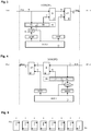
- the figure 3 is a block diagram of an embodiment of a synchronization unit before FSYNC of a processor PEi, where i is the rank of the processor in the chain.
- the processor comprises execution units 10 configured to react to machine instructions executed on the processor, in particular the group synchronization instruction.
- the processor also includes a bench of working registers, among which a register is dedicated to synchronization, which is called an IPE register (“Inter-Processor Event register”).
- IPE register Inter-Processor Event register
- a 64-bit IPE register can have a 16-bit forward event FE field, a 16-bit rear event BE field, a 16-bit FM mode field, and finally a mode BM field 16-bit reverse.
- the FE and FM fields are used, as well as the waitclrF and notifyF parameters of the synchronization instructions.
- the BE and BM fields of the IPE register, and the waitclrB and notifyB parameters are used by the BSYNC unit managing the rear notification link BN and described later.
- the FE field of the IPE register is configured to record the notifications arriving on the 16 incoming notification lines FNin, produced by the previous processor PEi-1. For example, each bit of the FE field, initially at “0”, changes to "1” when the corresponding notification line changes to "1", and the bit remains at “1” even if the line then changes to "0” .
- the 16 bits of the FM mode field of the IPE register form a first entry of an AND gate bit by bit 12, the other entry receiving the 16 incoming notification lines FNin.
- the 16-bit output of gate 12 contributes to the states of the 16 outgoing forward notification lines FNout, going to the following processor PEi + 1.
- the states of the incoming lines FNin can be individually blocked or propagated on the outgoing notification lines FNout according to the bits contained in the FM mode field.
- notifications emitted by the preceding processor PEi-1 can be propagated selectively to the following processor PEi + 1.
- the current processor PEi can also send forward notifications to the next processor.
- the bits of the notifyF parameter of a synchronization instruction executed by the processor PEi are combined at the output of the AND gate 12 by an OR gate bit by bit 14.
- any bit at "1" of the notifyF parameter is transmitted on a corresponding outgoing notification line, independently of the state of the corresponding bit of the output of AND gate 12.
- the processor When a synchronization instruction is executed by the processor PEi with a non-zero waitclrF parameter, the processor is put in a waiting state and the waitclrF parameter determines the condition required to bring the processor out of the waiting state. More specifically, the waitclrF parameter identifies, by respective bit positions, the notifications which must be received by the processor PEi. All incoming notifications are saved in the FE register field, including those that pass through the processor but are not intended for the processor. Thus, the content of the FE field is compared at 16 with the waitclrF parameter, so that the comparison produces a "true” result when the bits at "1" of the FE register field include the bits at "1" of the waitclrF parameter.
- the “true” result is taken into account by the execution units 10 of the processor so that the processor leaves the waiting state and continues the execution of its program. Furthermore, the “true” result of the comparison causes a reset of the bits of the FE register field corresponding to the bits at “1” of the waitclrF parameter so that a new wave of notifications can be taken into account.
- the figure 4 is a block diagram of an embodiment of the rear synchronization unit BSYNC of the processor PEi.
- This unit uses the BE and BM fields of the IPE register, and the waitclrB and notifyB parameters of the synchronization instruction, this to manage the rear notification links BN in a similar way to the unit of the figure 3 .
- the structure is symmetrical to process incoming notification lines BNin coming from the processor PEi + 1, and outgoing notification lines BNout going to the processor PEi-1.
- the FM and BM mode fields of the IPE registers of the processors can be initialized by an operating system at system startup, to configure groups of processors within which the processors synchronize with one another. Preferably, to reduce latency, each group is formed of consecutive processors in the chain.
- each PEi processor can send 16 different notifications to each of its two adjacent processors PEi-1, PEi + 1, and receive 16 different notifications from each of its two adjacent processors.
- all the downstream processors receive a corresponding notification sent by any one of the processors. If the chain is configured as a ring, as is the case with figure 2 , an infinite looping of the propagation is prevented by setting the corresponding bit to 0 in one of the mode fields.
- each processor at the end of a group is at the intersection of two adjacent groups. Indeed, even if this processor does not propagate a notification from one group to the other, it can itself send a notification to each of the groups, and receive a notification from each of the groups.
- the barrier involving at most four processors in a group, is embodied in each processor by a register having a bit for each processor in the group. As soon as a processor reaches the barrier, it notifies the other processors by positioning the bit associated with it in the registers of the other processors, then stops to wait for the other processors to reach the barrier. A stopped processor resumes its activity as soon as all the bits corresponding to the other processors are positioned in its register, starting by resetting the bits of the register.
- the figure 5 illustrates a configuration of the processors of the figure 2 allowing barrier type synchronization involving, for example, a group of eight consecutive processors 0 to 7 of the chain.
- a single front notification line and a single rear notification line can be used between each pair of adjacent processors in the group.
- the notification lines can be different from one pair of processors to another, it is assumed here, for the sake of clarity, that the notification lines used all have the same rank k, where k is between 0 and 15 - One thus uses a front notification line denoted FNk and a rear notification line denoted BNk between the pairs of processors.
- Processors 0 to 7 are all configured not to propagate notifications before FNk, that is to say that the bit of rank k of their register fields FE is 0. In other words, a processor of the group can only receive FNk notification from its immediate predecessor, as shown by right-angled arrows from inside the processors.
- processors 1 to 6 are configured to propagate rear notifications BNk, that is to say that the bit of rank k of their register fields BE is 1. This state is illustrated by horizontal arrows towards the left.
- each processor can always send any notification in both directions, and its register fields FE and BE record the notifications which pass through the processor.
- the processor 7 is illustrated with a bent arrow to the left indicating that it can send a rear notification BNk.
- the first two instructions can be implemented by a single SYNCGROUP instruction with waitclrF and notifyF parameters each identifying only rank k.
- the third instruction can be a SYNCGROUP instruction with all its null parameters except the waitclrB parameter which identifies only the rank k.
- These two instructions can be implemented by two consecutive SYNCGROUP instructions in which all the parameters are zero, except respectively the parameters notifyF and waitclrB, each identifying only the rank k.
- the two instructions can be implemented by a single SYNCGROUP instruction with waitclrF and notifyB parameters each identifying only the rank k.
- Processors 0 to 7 are thus put on hold as they reach the barrier. Processors 1 to 7, starting with executing a wait instruction, do not issue a notification until the barrier is lifted. Only processor 0 begins with a notification instruction FNk as soon as it reaches the barrier, before stopping in turn on a wait.
- the notification FNk sent by the processor 0 is recorded by the processor 1, which leaves its waiting state by sending a notification FNk to the next processor 2.
- Processor 1 is put on hold again, this time for a back notification BNk. Indeed, although processor 1 has reached the barrier, it is not known whether the other downstream processors have reached it.
- processor 7 sends a rear notification BNk to the processor 6, and continues its program.
- the barrier has been reached by all the processors, because the last processor 7 receives a notification only if all the preceding processors have issued one when reaching the barrier.
- This synchronization structure also opens up new perspectives for executing parallel processing, in particular loops whose iterations are not independent. Iterations are independent in a loop when their access to shared data like arrays is done on different elements.
- a classic multi-core structure allows to allocate several processors to execute in parallel several iterations of a loop. For example, each iteration of a loop of the following type is independent and can be assigned to a different core:
- the “barrier” directive designates a function conventionally available in the execution environment of multi-core processors, for example pthread_barrier_wait.
- variable a [2] will contain the new value whereas the first iteration needs the old value.
- the loop is executed by a single core, or else the loop is broken down into two parallel loops passing through a temporary table temp [] in the form:
- variables ii and t1 have a local scope limited to each loop body, while the arrays a [] and b [] are variables of global scope, shared by the processors.
- processor 0 executes:
- processor 7 which executes it:
- processors 0 to 7 are all configured not to propagate notifications before.
- processors 1 through 6 are configured to propagate back notifications.
- the waitclrF and notifyF parameters identify the notification lines used before, all of rank k in the example considered.
- the waitclrB and notifyB parameters identify the rear notification lines used, all also of rank k in the example considered.
- processor 0 executes:
- processor 1 executes in parallel:
- processor 0 reads the old value of the variable a [1]. It is important that this operation takes place before the variable a [1] has received the new value updated by processor 1 on line 8.
- the system is therefore configured and programmed so that line 8 is always executed after line 1.
- processor 0 On line 2, processor 0 notifies processor 1 that it has read the variable a [1]. (On line 3, processor 0 in principle waits for a rear notification to continue: this is issued by the syncgroup (notifyB) instruction executed by processor 7 before it enters the sub-loop.)
- the processor 1 is put on hold after having saved the new value of a [1] in a variable t1, and does not execute line 8 until the notification from processor 0 has been received.
- each processor releases the next processor after reading an old variable value, so that the next processor can update the variable.
- the last processor in the chain issues a back notification (syncgroup (notifyB)) during iteration, which frees the first processor to start a new iteration.
- each processor executes a last notification, which enables the processors still waiting to be unblocked, followed by a barrier-type synchronization necessary as in the case of a parallel loop.
- each processor executes two SYNCGROUP instructions, the first performing an operation of type "notify” and the second an operation of type "waitclr".
- SYNCGROUP instructions the first performing an operation of type "notify”
- waitclr the second an operation of type "waitclr”.
Landscapes
- Engineering & Computer Science (AREA)
- Theoretical Computer Science (AREA)
- Software Systems (AREA)
- Physics & Mathematics (AREA)
- General Engineering & Computer Science (AREA)
- General Physics & Mathematics (AREA)
- Computer Hardware Design (AREA)
- Mathematical Physics (AREA)
- Multi Processors (AREA)
- Hardware Redundancy (AREA)
Applications Claiming Priority (1)
| Application Number | Priority Date | Filing Date | Title |
|---|---|---|---|
| FR1874270A FR3091363B1 (fr) | 2018-12-27 | 2018-12-27 | Système de synchronisation inter-processeurs configurable |
Publications (3)
| Publication Number | Publication Date |
|---|---|
| EP3674898A1 true EP3674898A1 (de) | 2020-07-01 |
| EP3674898C0 EP3674898C0 (de) | 2025-09-24 |
| EP3674898B1 EP3674898B1 (de) | 2025-09-24 |
Family
ID=66690603
Family Applications (1)
| Application Number | Title | Priority Date | Filing Date |
|---|---|---|---|
| EP19214863.3A Active EP3674898B1 (de) | 2018-12-27 | 2019-12-10 | Konfigurierbares synchronisationssystem zwischen prozessoren |
Country Status (4)
| Country | Link |
|---|---|
| US (1) | US12141626B2 (de) |
| EP (1) | EP3674898B1 (de) |
| CN (1) | CN111382112B (de) |
| FR (1) | FR3091363B1 (de) |
Families Citing this family (4)
| Publication number | Priority date | Publication date | Assignee | Title |
|---|---|---|---|---|
| US11720360B2 (en) * | 2020-09-11 | 2023-08-08 | Apple Inc. | DSB operation with excluded region |
| CN112130904B (zh) * | 2020-09-22 | 2024-04-30 | 黑芝麻智能科技(上海)有限公司 | 处理系统、处理器间通信方法、以及共享资源管理方法 |
| CN113227975B (zh) * | 2021-03-31 | 2023-03-17 | 华为技术有限公司 | 一种同步方法及装置 |
| US12332682B2 (en) * | 2021-07-21 | 2025-06-17 | Q.M Technologies Ltd. | System and method for clock synchronization and time transfer between quantum orchestration platform elements |
Citations (3)
| Publication number | Priority date | Publication date | Assignee | Title |
|---|---|---|---|---|
| US5222229A (en) * | 1989-03-13 | 1993-06-22 | International Business Machines | Multiprocessor system having synchronization control mechanism |
| US20120179896A1 (en) * | 2011-01-10 | 2012-07-12 | International Business Machines Corporation | Method and apparatus for a hierarchical synchronization barrier in a multi-node system |
| US20150339256A1 (en) | 2014-05-21 | 2015-11-26 | Kalray | Inter-processor synchronization system |
Family Cites Families (9)
| Publication number | Priority date | Publication date | Assignee | Title |
|---|---|---|---|---|
| US4468734A (en) * | 1982-03-26 | 1984-08-28 | International Business Machines Corporation | Method of purging erroneous signals from closed ring data communication networks capable of repeatedly circulating such signals |
| US5163138A (en) * | 1989-08-01 | 1992-11-10 | Digital Equipment Corporation | Protocol for read write transfers via switching logic by transmitting and retransmitting an address |
| US6618117B2 (en) * | 1997-07-12 | 2003-09-09 | Silverbrook Research Pty Ltd | Image sensing apparatus including a microcontroller |
| US6775799B1 (en) * | 2000-03-17 | 2004-08-10 | Applied Micro Circuits Corporation | Protocol independent performance monitor with selectable FEC encoding and decoding |
| US20050120185A1 (en) * | 2003-12-01 | 2005-06-02 | Sony Computer Entertainment Inc. | Methods and apparatus for efficient multi-tasking |
| GB0407384D0 (en) * | 2004-03-31 | 2004-05-05 | Ignios Ltd | Resource management in a multicore processor |
| US7958497B1 (en) * | 2006-06-07 | 2011-06-07 | Replay Solutions, Inc. | State synchronization in recording and replaying computer programs |
| DE112006003895T5 (de) * | 2006-06-26 | 2009-06-10 | Mitsubishi Electric Corp. | Kommunikationsknoten und Token-Herausgabeverfahren und Token-Ringkommunikationsverfahren in einem Ring-Kommunikationssystem |
| US20120096292A1 (en) * | 2010-10-15 | 2012-04-19 | Mosaid Technologies Incorporated | Method, system and apparatus for multi-level processing |
-
2018
- 2018-12-27 FR FR1874270A patent/FR3091363B1/fr active Active
-
2019
- 2019-12-10 EP EP19214863.3A patent/EP3674898B1/de active Active
- 2019-12-25 CN CN201911353795.3A patent/CN111382112B/zh active Active
- 2019-12-27 US US16/729,118 patent/US12141626B2/en active Active
Patent Citations (3)
| Publication number | Priority date | Publication date | Assignee | Title |
|---|---|---|---|---|
| US5222229A (en) * | 1989-03-13 | 1993-06-22 | International Business Machines | Multiprocessor system having synchronization control mechanism |
| US20120179896A1 (en) * | 2011-01-10 | 2012-07-12 | International Business Machines Corporation | Method and apparatus for a hierarchical synchronization barrier in a multi-node system |
| US20150339256A1 (en) | 2014-05-21 | 2015-11-26 | Kalray | Inter-processor synchronization system |
Also Published As
| Publication number | Publication date |
|---|---|
| EP3674898C0 (de) | 2025-09-24 |
| CN111382112A (zh) | 2020-07-07 |
| US20200210248A1 (en) | 2020-07-02 |
| FR3091363B1 (fr) | 2021-08-06 |
| CN111382112B (zh) | 2025-07-15 |
| EP3674898B1 (de) | 2025-09-24 |
| FR3091363A1 (fr) | 2020-07-03 |
| US12141626B2 (en) | 2024-11-12 |
Similar Documents
| Publication | Publication Date | Title |
|---|---|---|
| EP3674898B1 (de) | Konfigurierbares synchronisationssystem zwischen prozessoren | |
| US10679210B2 (en) | Blockchain transaction commitment ordering | |
| US7676669B2 (en) | Multi-core processor control method | |
| EP0029131B1 (de) | Steuerungsverfahren zur Mittelzuteilung in einem simultan arbeitenden Mehrrechnersystem | |
| CN106462395B (zh) | 多线程处理器架构中的线程等待 | |
| US10528494B2 (en) | Direct memory access (“DMA”) descriptor processing using identifiers assigned to descriptors on DMA engines | |
| FR3072801A1 (fr) | Synchronisation dans une matrice de traitement a paves multiples | |
| EP2947577B1 (de) | Synchronisationssystem zwischen prozessoren | |
| US8281107B2 (en) | Method of sharing coarse grained array and processor using the method | |
| EP2839378A1 (de) | System und verfahren zur verwaltung von cache-kohärenz in einem netzwerk aus mit cache-speichern ausgerüsteten prozessoren | |
| US20190042946A1 (en) | Triggered operations to improve allreduce overlap | |
| US9342564B2 (en) | Distributed processing apparatus and method for processing large data through hardware acceleration | |
| CN108984277A (zh) | 基于gps原子钟的分布式数据库事务处理方法及装置 | |
| FR2865290A1 (fr) | Procede de gestion de donnees dans un processeur matriciel et processeur matriciel mettant en oeuvre ce procede | |
| US20090043991A1 (en) | Scheduling Multithreaded Programming Instructions Based on Dependency Graph | |
| CN106569968B (zh) | 用于可重构处理器的阵列间数据传输结构与调度方法 | |
| CN110135178A (zh) | 区块链验证中的零延迟账本访问技术 | |
| JP3008223B2 (ja) | プロセッサ間の同期処理装置 | |
| US20200210247A1 (en) | Computer System with Concurrency For Multithreaded Applications | |
| EP2431875A1 (de) | Prozessor auf einem elektronischen Chip, der mit einem materiellen Echtzeit-Monitor ausgestattet ist | |
| FR3065550A1 (fr) | Procede d'echange protege de donnees entre deux taches | |
| CN116010121A (zh) | 基于环形链表的多线程消息数据存取方法及装置 | |
| CN115374052A (zh) | 用于可重构密码阵列的任务处理方法及装置 | |
| CN119376684B (zh) | 数据链路处理方法、装置、设备、介质及产品 | |
| FR3045866A1 (fr) | Calculateur comprenant un processeur multi-coeurs et un procede de controle |
Legal Events
| Date | Code | Title | Description |
|---|---|---|---|
| PUAI | Public reference made under article 153(3) epc to a published international application that has entered the european phase |
Free format text: ORIGINAL CODE: 0009012 |
|
| STAA | Information on the status of an ep patent application or granted ep patent |
Free format text: STATUS: THE APPLICATION HAS BEEN PUBLISHED |
|
| AK | Designated contracting states |
Kind code of ref document: A1 Designated state(s): AL AT BE BG CH CY CZ DE DK EE ES FI FR GB GR HR HU IE IS IT LI LT LU LV MC MK MT NL NO PL PT RO RS SE SI SK SM TR |
|
| AX | Request for extension of the european patent |
Extension state: BA ME |
|
| RIN1 | Information on inventor provided before grant (corrected) |
Inventor name: ODINOT, ARNAUD Inventor name: DUPONT DE DINECHIN, BENOIT Inventor name: RAY, VINCENT |
|
| STAA | Information on the status of an ep patent application or granted ep patent |
Free format text: STATUS: REQUEST FOR EXAMINATION WAS MADE |
|
| 17P | Request for examination filed |
Effective date: 20201211 |
|
| RBV | Designated contracting states (corrected) |
Designated state(s): AL AT BE BG CH CY CZ DE DK EE ES FI FR GB GR HR HU IE IS IT LI LT LU LV MC MK MT NL NO PL PT RO RS SE SI SK SM TR |
|
| GRAP | Despatch of communication of intention to grant a patent |
Free format text: ORIGINAL CODE: EPIDOSNIGR1 |
|
| STAA | Information on the status of an ep patent application or granted ep patent |
Free format text: STATUS: GRANT OF PATENT IS INTENDED |
|
| INTG | Intention to grant announced |
Effective date: 20250429 |
|
| GRAS | Grant fee paid |
Free format text: ORIGINAL CODE: EPIDOSNIGR3 |
|
| GRAA | (expected) grant |
Free format text: ORIGINAL CODE: 0009210 |
|
| STAA | Information on the status of an ep patent application or granted ep patent |
Free format text: STATUS: THE PATENT HAS BEEN GRANTED |
|
| AK | Designated contracting states |
Kind code of ref document: B1 Designated state(s): AL AT BE BG CH CY CZ DE DK EE ES FI FR GB GR HR HU IE IS IT LI LT LU LV MC MK MT NL NO PL PT RO RS SE SI SK SM TR |
|
| REG | Reference to a national code |
Ref country code: GB Ref legal event code: FG4D Free format text: NOT ENGLISH |
|
| REG | Reference to a national code |
Ref country code: CH Ref legal event code: EP |
|
| REG | Reference to a national code |
Ref country code: DE Ref legal event code: R096 Ref document number: 602019076056 Country of ref document: DE |
|
| U01 | Request for unitary effect filed |
Effective date: 20251016 |
|
| U07 | Unitary effect registered |
Designated state(s): AT BE BG DE DK EE FI FR IT LT LU LV MT NL PT RO SE SI Effective date: 20251022 |