EP3674756A1 - Display body, anti-counterfeiting thread paper, and anti-counterfeiting medium - Google Patents
Display body, anti-counterfeiting thread paper, and anti-counterfeiting medium Download PDFInfo
- Publication number
- EP3674756A1 EP3674756A1 EP18847815.0A EP18847815A EP3674756A1 EP 3674756 A1 EP3674756 A1 EP 3674756A1 EP 18847815 A EP18847815 A EP 18847815A EP 3674756 A1 EP3674756 A1 EP 3674756A1
- Authority
- EP
- European Patent Office
- Prior art keywords
- display
- visible light
- optical resonance
- counterfeiting
- light
- Prior art date
- Legal status (The legal status is an assumption and is not a legal conclusion. Google has not performed a legal analysis and makes no representation as to the accuracy of the status listed.)
- Granted
Links
Images





Classifications
-
- G—PHYSICS
- G02—OPTICS
- G02B—OPTICAL ELEMENTS, SYSTEMS OR APPARATUS
- G02B5/00—Optical elements other than lenses
- G02B5/008—Surface plasmon devices
-
- G—PHYSICS
- G09—EDUCATION; CRYPTOGRAPHY; DISPLAY; ADVERTISING; SEALS
- G09F—DISPLAYING; ADVERTISING; SIGNS; LABELS OR NAME-PLATES; SEALS
- G09F19/00—Advertising or display means not otherwise provided for
- G09F19/12—Advertising or display means not otherwise provided for using special optical effects
-
- B—PERFORMING OPERATIONS; TRANSPORTING
- B42—BOOKBINDING; ALBUMS; FILES; SPECIAL PRINTED MATTER
- B42D—BOOKS; BOOK COVERS; LOOSE LEAVES; PRINTED MATTER CHARACTERISED BY IDENTIFICATION OR SECURITY FEATURES; PRINTED MATTER OF SPECIAL FORMAT OR STYLE NOT OTHERWISE PROVIDED FOR; DEVICES FOR USE THEREWITH AND NOT OTHERWISE PROVIDED FOR; MOVABLE-STRIP WRITING OR READING APPARATUS
- B42D25/00—Information-bearing cards or sheet-like structures characterised by identification or security features; Manufacture thereof
- B42D25/30—Identification or security features, e.g. for preventing forgery
- B42D25/328—Diffraction gratings; Holograms
-
- B—PERFORMING OPERATIONS; TRANSPORTING
- B42—BOOKBINDING; ALBUMS; FILES; SPECIAL PRINTED MATTER
- B42D—BOOKS; BOOK COVERS; LOOSE LEAVES; PRINTED MATTER CHARACTERISED BY IDENTIFICATION OR SECURITY FEATURES; PRINTED MATTER OF SPECIAL FORMAT OR STYLE NOT OTHERWISE PROVIDED FOR; DEVICES FOR USE THEREWITH AND NOT OTHERWISE PROVIDED FOR; MOVABLE-STRIP WRITING OR READING APPARATUS
- B42D25/00—Information-bearing cards or sheet-like structures characterised by identification or security features; Manufacture thereof
- B42D25/30—Identification or security features, e.g. for preventing forgery
- B42D25/36—Identification or security features, e.g. for preventing forgery comprising special materials
- B42D25/378—Special inks
-
- B—PERFORMING OPERATIONS; TRANSPORTING
- B42—BOOKBINDING; ALBUMS; FILES; SPECIAL PRINTED MATTER
- B42D—BOOKS; BOOK COVERS; LOOSE LEAVES; PRINTED MATTER CHARACTERISED BY IDENTIFICATION OR SECURITY FEATURES; PRINTED MATTER OF SPECIAL FORMAT OR STYLE NOT OTHERWISE PROVIDED FOR; DEVICES FOR USE THEREWITH AND NOT OTHERWISE PROVIDED FOR; MOVABLE-STRIP WRITING OR READING APPARATUS
- B42D25/00—Information-bearing cards or sheet-like structures characterised by identification or security features; Manufacture thereof
- B42D25/30—Identification or security features, e.g. for preventing forgery
- B42D25/36—Identification or security features, e.g. for preventing forgery comprising special materials
- B42D25/378—Special inks
- B42D25/387—Special inks absorbing or reflecting ultraviolet light
-
- G—PHYSICS
- G02—OPTICS
- G02B—OPTICAL ELEMENTS, SYSTEMS OR APPARATUS
- G02B5/00—Optical elements other than lenses
- G02B5/02—Diffusing elements; Afocal elements
-
- G—PHYSICS
- G02—OPTICS
- G02B—OPTICAL ELEMENTS, SYSTEMS OR APPARATUS
- G02B5/00—Optical elements other than lenses
- G02B5/18—Diffraction gratings
- G02B5/1861—Reflection gratings characterised by their structure, e.g. step profile, contours of substrate or grooves, pitch variations, materials
-
- G—PHYSICS
- G09—EDUCATION; CRYPTOGRAPHY; DISPLAY; ADVERTISING; SEALS
- G09F—DISPLAYING; ADVERTISING; SIGNS; LABELS OR NAME-PLATES; SEALS
- G09F3/00—Labels, tag tickets, or similar identification or indication means; Seals; Postage or like stamps
- G09F3/02—Forms or constructions
Definitions
- the present invention relates to a display using optical resonance, such as surface plasmon resonance, and relates to anti-counterfeiting thread paper and an anti-counterfeiting medium to which the display is applied.
- optical resonance such as surface plasmon resonance
- Articles such as valuable securities, certificates, brand products, expensive products, electronic devices or individual certification media are desired to be difficult to counterfeit to protect the value and information of the articles from others.
- displays or media which are difficult to counterfeit may be affixed to such articles.
- media which display image information using a plurality of cells defined by a diffraction grating.
- displays which include a micro-image in specific cells among the plurality of cells.
- the micro-image corresponds to a bitmap pattern having two or more levels and can be observed, for example, by a microscope (e.g., see JP 2008-83226 A ).
- JP 2016-503356 A has an issue that a display exerting a similar watermark effect can be produced by partially and finely providing color-ink printing.
- Embodiments of the present invention have been made in light of the circumstances set forth above and each aim to provide a display capable of preventing production of imitation products by use of color inks and which is capable of more reliably detecting counterfeiting or imitation, and to provide anti-counterfeiting thread paper and an anti-counterfeiting medium to which the display is applied.
- the display that achieves the aim set forth above is a display using optical interaction and including an optical resonance structure layer provided with an embossed layer and a metal layer.
- the metal layer covers bottoms of concavities and tops of convexities of asperities formed in the embossed layer; an optical resonance region, in which the asperities are covered with the metal layer, resonates with incident light;
- the display is provided with fluorescent printing so as to overlap with the optical resonance region, the fluorescent printing permitting visible light to emerge when light outside the visible light range is incident thereon; and a color of visible light emerging due to light outside the visible light range being incident on the fluorescent printing is similar to a color of light transmitted therethrough due to the optical resonance.
- a motif is recorded in conformity with a contour of an optical resonance region of the optical resonance structure layer, the optical resonance region being provided with asperities, and the motif is displayed with a unique color due to optical resonance with visible light.
- the fluorescent printing contains an optical material that allows visible light to emerge when light outside a visible light range is incident on the material.
- light outside the visible light range includes at least any of ultraviolet rays, infrared rays, X-rays and radioactivity.
- a half width of a wavelength peak of visible light produced due to light outside the visible light range being incident on the fluorescent printing is larger than a half width of light transmitted therethrough due to the optical resonance.
- Anti-counterfeiting thread paper is configured by incorporating an anti-counterfeiting thread into a paper layer, the anti-counterfeiting thread including any one of the above displays, the display being provided with an adhesive layer at at least either a first surface or a second surface thereof.
- the anti-counterfeiting thread paper at least either of a front surface and a back surface of the paper layer is provided with a window for exposing the anti-counterfeiting thread incorporated into the paper layer.
- An anti-counterfeiting medium is configured by affixing a display to an article via an adhesive layer, the display being any one of the above displays and being provided with the adhesive layer at at least either a first surface or a second surface thereof.
- the display of any one of the embodiments of the present invention enables observation of both the color due to optical resonance, such as surface plasmon resonance, occurring in the optical resonance structure layer, and the color of the fluorescent printing by simultaneously applying visible light and light outside the visible light range to the display.
- optical resonance such as surface plasmon resonance
- the optical resonance in the optical resonance region of the optical resonance structure layer has low dependency on the light incident angle. Accordingly, there is no color change depending on the observation conditions and thus high visibility is ensured. Therefore, authenticity is easily verified.
- a diffractive structure to the embossed layer enables observation of three luminescent colors, i.e., the luminescent color of optical resonance, such as surface plasmon resonance, occurring in the optical resonance region of the optical resonance structure layer, the luminescent color of the fluorescent printing, and the iridescent color of diffracted light of the diffractive structure.
- the luminescent color of optical resonance such as surface plasmon resonance
- anti-counterfeiting thread paper or an anti-counterfeiting medium that can easily verify authenticity can be produced.
- the counterfeit product may appear to have a similar color when observed; however, when the counterfeit product is observed from the opposite side by holding it up to light, no color change occurs in the counterfeit product.
- the transmitted light develops a completely different color
- the fluorescent printing which develops no color in visible light, develops color when ultraviolet rays are applied thereto.
- any one of the embodiments of the present invention achieves a display capable of preventing production of imitation products by use of color inks and is capable of more reliably detecting counterfeiting or imitation, and achieves anti-counterfeiting thread paper and an anti-counterfeiting medium to which the display is applied.
- information referred to in the following embodiments of the present invention corresponds to any of motifs, characters, numerals, a combination of motifs and characters, a combination of characters and numerals, a combination of numerals and motifs, and a combination of motifs, numerals and characters. Furthermore, symbols, marks, and the like other than the information mentioned above may be used.
- Fig. 1 is a cross-sectional view illustrating an example of a display 10 according to a first embodiment of the present invention.
- the display 10 may include a carrier 1, an optical resonance structure layer 2 and a fluorescent printing 5.
- the carrier 1 holds the optical resonance structure layer 2.
- a plastic film transmitting visible light may be used as a material for the carrier 1.
- the plastic film may absorb ultraviolet rays.
- the plastic film may be a polyethylene terephthalate film, a polyethylene naphthalate film, a polyimide film, a polyethylene film, a polypropylene film, a heat resistant vinyl chloride film, or the like.
- polyethylene terephthalate resin may further be used due to having high heat resistance and a stable thickness.
- the optical resonance structure layer 2 includes an embossed layer 2a laminated to the carrier 1, and a metal layer 4 provided onto the embossed layer 2a.
- the embossed layer 2a has a surface facing away from the carrier 1, on which a microstructure 3 constituted of micro-asperities is formed.
- the region in the optical resonance structure layer 2 where the microstructure 3 is formed is an optical resonance region. In the optical resonance region, the metal layer 4 on the microstructure 3 resonates with light and the light produced by resonance is transmitted, diffused or reflected.
- the embossed layer 2a is formed as a resin layer on one surface of the carrier 1.
- the resin may be a thermoplastic resin, a thermosetting resin, an ultraviolet-curable resin, an electron beam-curable resin, or the like.
- the thermoplastic resin may be an acrylic resin, an epoxy resin, a cellulose resin, a vinyl resin, or the like.
- the resin may be a urethane resin formulated by adding polyisocyanate as a cross-linking agent to an acrylic polyol, polyester polyol or the like having a reactive hydroxyl group for crosslinkage, or a melamine-based resin, a phenol-based resin, or the like.
- the ultraviolet- or electron beam-curable resin may be epoxy (meth)acrylate, urethane (meth)acrylate, or the like. These resins may be applied by a known application method, such as gravure printing, micro gravure printing, or the like.
- the microstructure 3 is formed by pressing a plate, on which a microstructure is formed, against the embossed layer 2a.
- a master plate for the pressing plate having a microstructure may be formed by applying an electron beam to a surface of an electron beam-curable resin, exposing the resin to produce a desired pattern (microstructure pattern) and developing the exposed pattern. Then, a metal film may be formed on a surface of the master plate by electroplating to duplicate the pattern of asperities of the relief master plate, for usage as a pressing plate. Alternatively, the pattern of asperities may be directly formed on a metal plate by using a laser beam, for usage as a pressing plate.
- the microstructure 3 is formed on a surface of the embossed layer 2a by thermally pressing the pressing plate formed by either of the methods against the embossed layer 2a, or by curing an uncured curable resin, with a pressing plate being brought into close contact therewith.
- Resin materials for the embossed layer 2a or methods of forming the microstructure 3 are not limited to those mentioned above.
- the microstructure 3 may have convexities each having a rectangular cross section.
- convexities of the microstructure 3 according the embodiment of the present invention may each have a cross section that is not limited to a rectangular shape but may have a cross section of any desired shape as long as surface plasmon excitation occurs due to entry of visible light into the microstructure 3 and the metal layer 4 and there occurs a phenomenon of changing color before and after entry of visible light due to optical resonance.
- the cross section of the convexities of the microstructure 3 may each have a shape based on a cone, three-sided pyramid, column, rectangular parallelepiped, or the like.
- convexities of the microstructure 3 each have a rectangular cross section as shown in Fig. 1
- surface plasmon excitation may easily occur under conditions that the convexities each have a height H in the range of 20 nm or more and 800 nm, and more preferably 50 nm or more and 600 nm or less, and the convexities, if periodically formed, are arranged at an interval P in the range, for example, of 50 nm or more and 1,000 nm or less, and more preferably 100 nm or more and 600 nm or less.
- the metal layer 4 is formed on the microstructure 3.
- the metal layer 4 may be formed by forming a metal film using a vacuum deposition method. With this method, a film can be formed on the embossed layer 2a without filling the asperities of the microstructure 3.
- Metal or a metal compound used for the metal layer 4 may be gold, silver, titanium nitride, aluminum or the like.
- the vacuum deposition method may be vacuum vapor deposition, sputtering, or the like.
- the metal layer 4 may have a thickness in the range of 20 nm or more and 100 nm or less. To achieve even more suitable light transmittance or to prevent defects, such as cracking, the metal layer 4 may have a thickness in the range of 40 nm or more and 60 nm or less.
- the metal layer 4 may be provided across the surface of the microstructure 3.
- the metal layer 4 may be partially provided to the microstructure 3.
- a metal layer may be provided across the surface of the microstructure 3 first by a vacuum deposition method, followed by selectively etching and removing portions where the metal layer 4 is not required.
- a mask may be used for the selective removal.
- the mask may be obtained by printing, or may be a mask on which an inorganic compound layer is partially formed.
- the partially provided metal layer 4 may have an outer shape of a curve.
- the outer shape may be a geometric pattern.
- the geometric pattern may be a colored geometric pattern.
- the metal layer 4 may also be formed on a portion where the microstructure 3 is not formed.
- the metal layer 4 may have a thickness that is determined considering the influence of this case.
- the thickness of the metal film may vary depending on the surface configuration of an object on which the film is deposited even when the processing conditions are constant.
- a surface configuration is formed with accurate control. Therefore, thickness variation of a metal film to be formed on asperities of various shapes can be estimated at the stage of designing the asperities by conducting verification experiments in advance. Accordingly, if thickness variation occurs in the metal film 4 due to variation in the microscopic asperities, a desired color can be achieved as a result of optical resonance that is caused by surface plasmon excitation or the like which is due to entry of visible light into the optical resonance structure layer 2.
- the fluorescent printing 5 is provided to a surface of the carrier 1 facing away from the optical resonance structure layer 2.
- the fluorescent printing 5 is made of a binder resin comprising an organic polymer material in which a luminescent material is dissolved or dispersed.
- the luminescent material converts light, such as ultraviolet rays, infrared rays, X-rays or radioactivity, outside the range of visible light into visible light and becomes luminous.
- the luminescent material may be a fluorophore or phosphor, or a luminescent material that emits light due to external stimulation. Of these materials, a material that can be easily handled in actual use and emits light when irradiated with ultraviolet rays or infrared rays may be used.
- the binder resin may be an acrylic resin, a vinyl resin, a polyester resin, a urethane resin, or the like.
- Fluorescence refers to emission of light near the visible range caused by external stimulation (excitation).
- excitation external stimulation
- phosphorescence generally refers to emission of light whose duration seen by the eyes after excitation ceases has some duration (about 0.1 second) or more
- luminescence generally refers to emission of light whose duration seen by the eyes is particularly long
- emission of light other than these is generally referred to as fluorescence.
- Any of the materials for fluorescence, phosphorescence and luminescence may be applied to the embodiment of the present invention. However, a fluorescent material may be applied to the embodiment of the present invention due to the desired purpose.
- the fluorescent material may be an inorganic material, an organic material, a complex, or the like.
- Examples of the fluorescent material are as follows.
- a fluorescent agent which emits light when irradiated with ultraviolet rays may be an agent that is excited by ultraviolet rays and has a spectrum peak in the wavelength range of blue, green, red, or the like, when returning to an energy level lower than during excitation.
- An example of the inorganic material may be a material that is obtained by adding a small amount of metal (copper, silver, manganese, bismuth, lead, or the like) as an activator to a high purity fluorophore that is zinc sulfide or a sulfide of an alkaline earth metal to increase emission, followed by high temperature baking.
- the degree of hue, brightness, or color decay can be controlled.
- the organic material include a cyanine dye, a coumarin dye, a rhodamine dye, and the like. Fluorescent sites may be modified on the binder resin.
- a fluorescent agent which emits light when irradiated with infrared rays may be an infrared-visible conversion fluorescent agent which is excited by infrared rays and becomes visibly luminous, or an agent which is excited by infrared rays and becomes luminous with a longer wavelength.
- the infrared-visible conversion fluorescent agent has an extraordinarily peculiar excitation mechanism. This fluorescent agent excites a plurality of infrared photons having small energy to permit them to be visibly luminous.
- These light emission mechanisms may be classified into two types. One is a mechanism which enables high excitation by multistage excitation of activator ions, and the other is a mechanism which enables high excitation by multiple resonance energy transfer from a sensitizer.
- the former is a mechanism that is observed in many host crystals using Er 3+ or Ho 3+ as an activator.
- the latter is a mechanism in which a sensitizer Yb 3+ absorbs infrared rays and excites Er 3+ , Tm 3+ , Ho 3+ or the like in the emission center at a high level by multistage energy transfer.
- the fluorescent printing 5 is formed in a region overlapping with the region where asperities are formed in plan view.
- the fluorescent printing 5 may be formed, in particular, within the region where asperities are formed.
- the color of the emission wavelength of the fluorescent printing 5 may be a color similar to that of light resonating in the optical resonance region.
- the expression "color similar to” refers to a color whose difference in center wavelength of the emission wavelength or the resonance wavelength is 50 nm or less. The difference in this case may be 5 nm or more.
- the transmittance of the emission wavelength range in the resonance wavelength range may be 50% or more. The transmittance in this case may be 95% or less.
- a half width of a wavelength peak of visible light produced due to the light outside the visible light range being incident on the fluorescent printing may be more than a half width of light transmitted therethrough due to the optical resonance.
- the range of light transmitted through the fluorescence wavelength range by optical resonance can be selectively filtered.
- the color of light transmitted through the optical resonance region may be similar to the color of the fluorescent printing 5, but luminance may be different between these colors.
- similar colors may each appear as patterns having different luminance and the impression of the motif may change between front and back.
- the ultraviolet rays that have excited the fluorophore of the fluorescent printing 5 are not transmitted through the metal layer 4 where the asperities are formed. Therefore, the motif of the fluorescent printing 5 can be observed only when ultraviolet rays are applied from the fluorescent printing 5 side, and cannot be observed when ultraviolet rays are applied from the metal layer 4 side.
- Ultraviolet rays that have been applied to the display 10 and have not been absorbed by the fluorescent printing 5 are reflected by the metal layer 4 and can be reused as excitation light for the fluorescent printing 5. Of the light emerging from the fluorescent printing 5, light that has emerged in the direction of the carrier 1 is guided through the carrier 1 and cannot be observed.
- the light incident on the asperities is prevented from being specularly reflected but is transmitted or scattered, and therefore fluorescence is prevented from being guided. Since guided light is observed as being flared, ghosting may occur in the fluorescent motif.
- provision of a plasmon structure to the other surface of the fluorescent printing 5 as in the configuration of the present invention can achieve a clear image without ghosting.
- the metal layer 4 may be partially provided.
- a motif can be formed with or without the effects of the plasmons and the fluorescent printing 5.
- the portions where there is no metal layer 4 may be filled with a resin, such as an adhesive layer, so that fluorescence is guided.
- the surface of the filled-in resin facing away from the metal layer 4 can be an interface with the air.
- the opposite surface via the filled-in resin and the metal layer 4 can also be an interface with the air.
- the metal layer 4 and the motif of the fluorescent printing 5 can be made transparent. With this configuration, fluorescence can be easily guided through the resin with which the fluorescent printing 5 is in contact.
- Fig. 2 is a cross-sectional view illustrating an example of a display 11 according to a second embodiment of the present invention.
- the fluorescent printing 5 is arranged being embedded in the optical resonance structure layer 2 and in contact with the carrier 1.
- the remaining configuration is the same as the display 10.
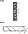
- Fig. 3 is a plan view illustrating the display 10 or 11 observed from the carrier 1 side (observed from the upper side in Fig. 1 or 2 ) in a state in which visible light and light outside the visible light range are applied to the display 10 or 11.
- a region A corresponds to a region that has developed color due to visible light being incident on the microstructure 3 of the optical resonance structure layer 2 and causing optical resonance in the optical resonance structure layer 2.
- the shape of characters "500” corresponds to the shape of the fluorescent printing 5 arranged facing the carrier 1.
- Fig. 3 shows a state in which light outside the visible light range is incident on the fluorescent printing 5 and visible light emerges from the fluorescent printing 5 so that the characters "500" appear.
- the color developed due to optical resonance, such as surface plasmon resonance, in the optical resonance region, and the similar-color light of the fluorescent printing 5 on the back surface can both be observed from the carrier 1 side of the display 10 or 11.
- the optical resonance structure layer 2 has low dependence on the incident light angle. Accordingly, there is little change in color depending on observation conditions and thus high visibility is ensured. Therefore, authenticity can be easily determined.
- Fig. 4 is a partially enlarged cross-sectional view illustrating the optical resonance structure layer 2 as a specific configuration example of the microstructure 3 formed on a surface of the embossed layer 2a facing away from the carrier 1, and the metal layer 4 formed on the microstructure 3.
- the configuration shown in Fig. 4 is common to both of the displays 10 and 11.
- the microstructure 3 has convexities and concavities.
- the metal layer 4 formed on the microstructure 3 covers bottoms of the concavities of the microstructure 3 and tops of the convexities thereof.
- Fig. 4 shows a microstructure 3 whose convexities each have a rectangular cross section.
- the cross section does not have to be precisely rectangular.
- the cross section may be rounded rectangular.
- the cross section of each convexity of the microstructure 3 is not limited to a rectangular shape but may be any desired shape based on a cone, three-sided pyramid, column, rectangular parallelepiped, or the like as long as the surface plasmons are excited due to interaction with visible light that is incident on the metal layer 4 on the microstructure 3 and there occurs a phenomenon in which the observable color is different before and after entry of visible light due to the optical resonance caused by the excited surface plasmons.
- convexities of the microstructure 3 each have a rectangular cross section as shown in Fig. 4
- surface plasmon excitation may easily occur under conditions that the convexities each have a height H in the range of 20 nm or more and 800 nm, and more preferably 50 nm or more and 600 nm or less, and the convexities, if periodically formed, are arranged at an interval P in the range, for example, of 50 nm or more and 1,000 nm or less, and more preferably 100 nm or more and 600 nm or less.
- Fig. 5 is a cross-sectional view illustrating an example of a display 12 according to a third embodiment of the present invention.
- the display 12 is different from the display 10 only in the arrangement position of the fluorescent printing 5. Specifically, in the display 12, the fluorescent printing 5 is arranged facing the metal layer 4.
- Fig. 6 is a plan view of the display 12 observed from the fluorescent printing 5 side (observed from the lower side in Fig. 5 ) in a state in which visible light and light outside the visible light range are applied to the display 12.
- a region B corresponds to a region that has developed color due to visible light being incident on the microstructure 3 of the optical resonance structure layer 2 and causing optical resonance in the optical resonance structure layer 2.
- the shape of characters "500” corresponds to the shape of the fluorescent printing 5 arranged facing the metal layer 4.
- Fig. 3 shows a state in which light outside the visible light range is incident on the fluorescent printing 5 and visible light emerges from the fluorescent printing 5 so that the characters "500" appear.
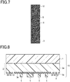
- Fig. 7 is a plan view of the display 12 observed from the carrier 1 side (observed from the upper side in Fig. 5 ) in a state in which visible light and light outside the visible light range are applied to the display 12.
- the characters "500” of Fig. 7 are also in a state in which light outside the visible light range is incident on the fluorescent printing 5 and visible light emerges from the fluorescent printing 5 so that the characters "500” appear.
- the fluorescent printing 5 is not formed on the carrier 1, the characters "500” as observed from the carrier 1 side (observed from the upper side in Fig. 5 ) as shown in Fig. 7 are less luminous, although they are legible, than the characters "500” observed from the fluorescent printing 5 side as shown in Fig. 6 .
- Fig. 8 is a cross-sectional view illustrating an example of a display 13 according to a fourth embodiment of the present invention.
- the display 13 is similar to the display 12. However, in the display 13, the embossed layer 2a is provided with two types of microstructures which are a microstructure 3a and a microstructure 3b.
- the microstructure 3a has a cross section in a sawtooth shape and the microstructure 3b has convexities each having a cross section in a rectangular shape.
- the microstructures 3a and 3b are different in cross-sectional shape.
- the microstructures 3a and 3b may both have a plasmon structure in which optical resonance is caused by visible light, although the produced colors are different.
- either one of the microstructures 3a and 3b may have a plasmon structure and the other one may have a structure that can exert an optical effect other than surface plasmon resonance.
- the structure that can exert an optical effect other than surface plasmon resonance may be a diffractive structure, blazed structure, Fresnel lens structure, moth eye structure, or the like. Such a structure is not particularly limited. Some of the structures mentioned above may be combined with each other.
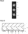
- Fig. 9 is a plan view of the display 13 observed from the carrier 1 side (observed from the upper side in Fig. 8 ) in a state in which visible light and light outside the visible light range are applied to the display 13.
- the microstructure 3a of the display 13 is a diffraction grating that produces diffracted light, while the microstructure 3b is a structure having asperities that generate surface plasmon resonance.
- a region C is a region that produces a color of diffracted light of the microstructure 3a serving as a diffraction grating.
- a region D is a region that produces a color of optical resonance, such as surface plasmon resonance, caused by the microstructure 3b.
- the characters "500" corresponding to the shape of the fluorescent printing 5 are presented by visible light.
- Fig. 10 is a cross-sectional view illustrating an example of a display 14 according to a fifth embodiment of the present invention.
- the display 14 is similar to the display 13. However, in the display 14, the embossed layer 2a is provided with a microstructure 3c and a microstructure 3d in addition to the microstructures 3a and 3b. In other words, the embossed layer 2a is provided with four types of microstructures 3a, 3b, 3c and 3d.
- the microstructures 3a, 3c and 3d of the display 13 are diffraction gratings that produce diffracted light, while the microstructure 3b is a structure having asperities that generate surface plasmon resonance.
- the microstructures 3a, 3c and 3d have grating periods different from each other.
- Fig. 11 is a plan view of the display 14 observed from the carrier 1 side (observed from the upper side in Fig. 10 ) in a state in which visible light and light outside the visible light range are applied to the display 14.
- a region E is a region that produces a color of diffracted light of the microstructure 3a serving as a diffraction grating.
- a region F is a region that produces a color of optical resonance caused by the microstructure 3b.
- a region G is a region that produces a color of diffracted light of the microstructure 3c serving as a diffraction grating.
- a region H is a region that produces a color of diffracted light of the microstructure 3d serving as a diffraction grating.
- a region I is a region that allows a character "0" or "5" corresponding to the shape of the fluorescent printing 5 to appear as a result of light outside the visible light range being incident on the fluorescent printing 5 and visible light emerging from the fluorescent printing 5.
- Fig. 12 is a plan view of the display 14 observed from the carrier 1 side (observed from the upper side in Fig. 10 ) in a state in which only visible light is applied to the display 14.
- the fluorescent printing 5 is not luminous because only visible light is applied and light outside the visible light range is not applied. Accordingly, in Figs. 12 , the region I shown in Fig. 11 does not appear.
- the display 14 allows the specific information of the characters "500” to appear by simultaneously applying both visible light and light outside the visible light range, but can hide part of the specific information of the characters "500” by applying only visible light.
- Fig. 13 is a cross-sectional view illustrating an example of an anti-counterfeiting transfer foil 20 according to a sixth embodiment of the present invention.
- a display according to any one of the embodiments of the present invention described above may be applied to the anti-counterfeiting transfer foil 20.
- the anti-counterfeiting transfer foil 20 in the example shown in Fig. 13 includes the carrier 1 and the optical resonance structure layer 2 of a display according to any one of the embodiments of the present invention. As shown, a release layer 6 is provided between the carrier 1 and the optical resonance structure layer 2, and an adhesive layer 7 is provided to the surface of the metal layer 4.
- the release layer 6 may be obtained by adding a lubricant to a resin.
- the resin may be a thermoplastic resin, a thermosetting resin, a moisture-curable resin, an ultraviolet-curable resin, an electron beam-curable resin, or the like.
- the resin may be an acrylic resin, a polyester resin, or a polyamide-imide resin.
- the lubricant may be a polyethylene powder or a wax, such as carnauba wax. These materials may be applied onto the carrier 1 using a known application method, such as gravure printing, micro gravure, or the like.
- the adhesive layer 7 may be a layer that adheres to the surface of an object to be transferred by heat and pressure and thus may be made of a known tackifying material, a thermosensitive adhesive material, or the like.
- a carrier film is applied to the carrier 1, for use as a film that transfers the display including the optical resonance structure layer 2.
- the display is of a type in which the fluorescent printing 5 is arranged on the surface of the metal layer 4 as shown in Fig. 5 , 8 or 10 (display 12, 13 or 14).
- the display applied to the anti-counterfeiting transfer foil 20 is not limited to the display having such a structure, but may be a display having a structure shown in Fig. 1 or 2 (display 10 or 11).
- Fig. 14 is a cross-sectional view illustrating an example of anti-counterfeiting paper 21 to which the anti-counterfeiting transfer foil 20 has been transferred, and from which the release layer 6 and the carrier 1 have been released.
- the anti-counterfeiting paper 21 shown in Fig. 14 is produced by transferring the anti-counterfeiting transfer foil 20 as shown in Fig. 13 to a transfer target substrate 8. Therefore, the anti-counterfeiting transfer foil 20 is configured by temporarily forming the optical resonance structure layer 2 of the display on the carrier 1, i.e., a carrier film, and then transferring the optical resonance structure layer 2 onto the transfer target substrate 8 made of paper or a plastic film by heat and pressure.
- Fig. 15 is a plan view illustrating an example of the anti-counterfeiting paper 21.
- the anti-counterfeiting paper 21 can be designed as desired.
- a printed layer 30 on which "500 yen" is printed is provided to the ant-counterfeiting paper 21.
- the optical resonance structure layer 2 may be provided in the vertical direction in the figure, i.e., in the longitudinal direction of an anti-counterfeiting thread 25.
- the printing 30 is provided by printing an ink.
- the printing 30 may be a printing of characters or a motif and can be added onto the carrier 1 or the transfer target substrate 8.
- the characters or the motif can be printed by a known printing method, such as offset printing, gravure printing or relief printing, by using a known ink material, such as an offset ink, a gravure ink or a relief ink, suitable for the printing method.
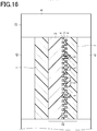
- Fig. 16 is a cross-sectional view illustrating an example of anti-counterfeiting paper 22 according to a seventh embodiment of the present invention.
- the anti-counterfeiting paper 22 shown in Fig. 16 is produced by incorporating an anti-counterfeiting thread 25 into a paper substrate 9 so as to appear from a window.
- the anti-counterfeiting thread 25 has a configuration in which a display according to any one of the embodiments of the present invention described above is provided to at least either of the surface of the carrier 1 and the surface of the metal layer 4 via the adhesive layer 7.
- a portion where the anti-counterfeiting thread 25 is incorporated is provided with windows 40 and 41 at the top and bottom surfaces.
- the anti-counterfeiting thread 25 can be observed from both the front and back surfaces of the anti-counterfeiting paper 22 via the windows 40 and 41.
- the windows 40 and 41 may extend to portions where there is no microstructure 3.
- the material that can be used for the paper substrate 9 may be plant pulp such as of softwood, hardwood, cotton, rice, esparto, bagasse, hemp, flax, kenaf or cannabis, or synthetic fibers made of a plastic material, such as polyethylene terephthalate, polypropylene, polyacrylate or polyvinyl chloride.
- a water-diluted material obtained by beating a plant pulp or synthetic fibers in water is subjected to a paper-making process for entwinement, followed by dehydration and drying.
- the paper obtains interfiber strength due to hydrogen bonds between hydroxyl groups of cellulose that is the material of the paper.
- a loading material of the paper clay, talc, calcium carbonate, titanium dioxide, or the like may be used.
- rosin, alkyl ketene dimer, stearic anhydride, alkenyl succinic anhydride, waxes, or the like may be used.
- a modified starch polyvinyl alcohol, polyacrylamide, urea-formaldehyde, melamine-formaldehyde, polyethyleneimine, or the like may be used. These materials may be added to the water-diluted material as necessary.
- the paper-making method used for the anti-counterfeiting paper 22 may be an existing layering method used for plant fiber paper.
- paper is made by kneading fibers well, which have been sufficiently swollen with a water-diluted material having a material concentration in the range of 0.5% or more and 10% or less, and more preferably 1% or more and 2% or less, and having the kneaded material flow onto a screen or mesh wire part for laying thereon, followed by dehydration and heating of the material to evaporate water.
- a thread including the display according to any one of the embodiments of the present invention is placed between the upper surface and the lower surface of the paper substrate 9.
- Close-contact layering is then performed by dehydration and heating with the three layers being overlapped.
- the front and back of the wire part used for the layering process are provided with desired protrusions, so that the fibers are not placed on the protrusions during the layering process but are placed only on the remaining portions of the screen or mesh.
- the adhesive layer 7, in the case of being incorporated into the paper substrate 9 together with the anti-counterfeiting thread 25, may only need to adhere to the paper substrate at the time of drying during the paper making process.
- a known tackifying material or thermosensitive adhesive material may be used.
- the display configuring the anti-counterfeiting thread 25 shown in Fig. 16 is of a type in which the fluorescent printing 5 is arranged on the surface of the metal layer 4 as shown in Fig. 5 , 8 or 10 (display 12, 13 or 14).
- the configuration of the display is not limited to this but may be the configuration shown in Fig. 1 or 2 (display 10 or 11).
- Fig. 17 is a plan view illustrating an example of a front surface of the anti-counterfeiting paper 22.
- Fig. 18 is a plan view illustrating an example of a back surface of the anti-counterfeiting paper 22.
- the anti-counterfeiting thread 25 is exposed from three square windows 40a, 40b and 40c of the paper substrate 9.
- visible light is incident on the paper, hexangular stellate colored regions K attributed to the microstructure 3 appear.
- metallic glossy regions L due to the metal layer 4 can be observed.
- characters "OK" producing color attributed to the fluorescent printing 5 can be simultaneously observed.
- a window 41 is provided to a position corresponding to the position of the window 40c of the front surface. This window enables observation, from the back surface as well, of a region M having a color attributed to the microstructure 3 or observation of mirror-reversed characters "OK" producing color attributed to the fluorescent printing 5.
- a carrier 1 As a carrier 1, a polyethylene terephthalate (PET) film having a thickness of 50 ⁇ m was used. To one surface of the carrier 1, a fluorescent printing ink comprising the following composition was applied by screen printing and dried to form a fluorescent printing 5 in a shape of characters "500" and having a thickness of 3 ⁇ m.
- PET polyethylene terephthalate
- an optical resonance structure layer ink comprising the following composition was applied by gravure printing and dried to form an optical resonance structure layer 2 having a thickness of 3 ⁇ m.
- a metal plate was prepared as a matrix of a structure having asperities inverse of those of a microstructure 3 which was to be formed for causing surface plasmon excitation.
- This matrix metal plate with a thermal pressure being applied thereto, was pressed against the optical resonance structure layer 2 for embossing.
- a microstructure 3 as desired was formed on the optical resonance structure layer 2.
- a display 10 including an optical resonance structure layer 2 and a fluorescent printing was prepared.
- Acrylic resin 18.0 parts by weight UV luminous fluorescent agent 2.0 parts by weight Cyclohexanone 80.0 parts by weight
- the display 10 obtained in this way was placed on a desk so that the surface where the fluorescent printing 5 had been formed on the carrier 1 faced upward.
- the display 10 in this case was under an environment of natural light, such as sunlight, as visible light, or under an environment of artificial lighting, such as a white fluorescent lamp or a white LED.
- a red color due to optical resonance which was considered to be caused by surface plasmon excitation, was observed.
- artificial lighting such as a white fluorescent lamp or a white LED
- a white fluorescent lamp or a white LED was set up at the back surface of the display 10 (surface facing away from the carrier 1) to observe the illumination light transmitting through the display 10.
- optical resonance which was considered to be caused by surface plasmon excitation, occurred on the back surface, and a green color different from the initially observed color was produced on the observation-side surface.
- a red color is produced on a surface of the display 10 as a result of visible light being incident thereon and exerting wavelength conversion effect of optical resonance that is considered to be caused by surface plasmon excitation
- a green color may be simultaneously observed on the surface of the display 10 facing away from the surface where red color was observed.
- the light transmitted through the surface of the display 10 facing away from the visible light incident surface corresponded to a wavelength obtained by subtracting the wavelength of visible light that was observed on the incident surface from the wavelength of visible light, and that colors that were observed on the front and back surfaces of the display 10 were in a complementary color relationship.
- the counterfeit product may appear to be similarly red when observed; however, when the counterfeit product is observed from the opposite side by holding it up to light, no color change occurs, i.e., the red color remains unchanged, in the counterfeit product.
- the transmitted light is green, that is a completely different color.
- ultraviolet rays are applied to the fluorescent printing 5 which produces no color in visible light, a yellow color is produced therein.
- a carrier 1 As a carrier 1, a polyethylene terephthalate (PET) film having a thickness of 16 ⁇ m was used. To one surface of the carrier 1, a release layer ink comprising the following composition was applied by gravure printing and dried to form a release layer 6 having a thickness of 1 ⁇ m.
- PET polyethylene terephthalate
- an optical resonance structure layer ink comprising the following composition was applied by gravure printing and dried to form an optical resonance structure layer 2 having a thickness of 1 ⁇ m.
- a metal plate was prepared as a matrix of a structure having asperities inverse of those of a microstructure 3 which was to be formed for causing surface plasmon excitation.
- This matrix metal plate with a thermal pressure being applied thereto, was pressed against the optical resonance structure layer 2 for embossing.
- a microstructure 3 as desired was formed on the optical resonance structure layer 2.
- a fluorescent printing ink comprising the following composition was applied onto the metal layer 4 by screen printing and dried to form fluorescent printing 5 in a shape of characters "500" and having a thickness of 2 ⁇ m.
- an adhesive layer ink comprising the following composition was applied onto the fluorescent printing 5 and the entire exposed surface of the metal layer 4 by gravure printing and dried to form an adhesive layer 7 having a thickness of 6 ⁇ m.
- an anti-counterfeiting transfer foil 20 was prepared.
- Acrylic resin 19.5 parts by weight Polyethylene powder 0.5 parts by weight Methyl ethyl ketone 80.0 parts by weight
- Acrylic resin 18.0 parts by weight UV luminous fluorescent agent 2.0 parts by weight Methyl ethyl ketone 80.0 parts by weight
- a relief printing plate made of brass and having a rectangular transfer surface was loaded on a vertical transfer apparatus.
- the anti-counterfeiting transfer foil 20 was placed on OCR paper having a basis weight of 90 g/m 2 and serving as a transfer target substrate 8, so that the carrier 1 would be on top.
- the transfer foil 20 placed on the OCR paper was located right beneath the relief printing plate. Thermal transfer was performed in this state and the carrier 1 that was no longer needed was released to thereby prepare anti-counterfeiting paper 21.
- the anti-counterfeiting paper 21 prepared in this way was placed on a desk so that the surface where the anti-counterfeiting transfer foil 20 had been transferred faced upward.
- the anti-counterfeiting paper 21 in this case was under an environment of direct light, such as sunlight, as visible light, or under an environment of direct light of artificial lighting, such as a fluorescent lamp or a LED.
- direct light such as sunlight
- visible light or under an environment of direct light of artificial lighting, such as a fluorescent lamp or a LED.
- artificial lighting such as a white fluorescent lamp or a white LED
- a white fluorescent lamp or a white LED was set up at the back surface of the anti-counterfeiting paper 21 to observe, from the front surface, the illumination light transmitting through the paper substrate 9 and the display.
- optical resonance which was considered to be caused by surface plasmon excitation, occurred on a surface of the display facing away from the front surface, and a yellow color different from the initially observed color was produced on the observation-side surface.
- a violet color is produced on a surface of the anti-counterfeiting paper 21 as a result of visible light being incident on the display and exerting a wavelength conversion effect of optical resonance that is considered to be caused by surface plasmon excitation
- a yellow color may be simultaneously observed on the surface of the anti-counterfeiting paper 21 facing away from the surface where violet color was observed.
- the light transmitted through the surface of the display of the anti-counterfeiting paper 21 facing away from the visible light incident surface corresponded to a wavelength obtained by subtracting the wavelength of visible light that was observed on the incident surface from the wavelength of visible light, and that colors that were observed on the front and back surfaces of the display were in a complementary color relationship.
- the counterfeit product may appear to be similarly violet when observed; however, when the counterfeit product is observed from the opposite side by holding it up to light, no color change occurs, i.e., the violet color remains unchanged, in the counterfeit product.
- the transmitted light is yellow, that is a completely different color.
- ultraviolet rays are applied to the fluorescent printing 5 which has developed no color in visible light, an orange color is produced in the fluorescent printing 5.
- authenticity can be easily verified by these two inspections.
- a carrier 1 As a carrier 1, a polyethylene terephthalate (PET) film having a thickness of 12 ⁇ m was used. To one surface of the carrier 1, an optical resonance structure layer ink comprising the following composition was applied by gravure printing and dried to form an optical resonance structure layer 2 having a thickness of 1 ⁇ m.
- PET polyethylene terephthalate
- a metal plate was prepared as a matrix of a structure having asperities inverse of those of a microstructure 3 which was to be formed in a hexangular stellate shape (see Fig. 17 ) for causing surface plasmon excitation.
- This matrix metal plate with a thermal pressure being applied thereto, was pressed against the optical resonance structure layer 2 for embossing.
- a microstructure 3 as desired was formed on the optical resonance structure layer 2.
- a fluorescent printing ink comprising the following composition was applied onto the metal layer 4 by screen printing and dried to form fluorescent printing 5 in a shape of characters "500" and having a thickness of 2 ⁇ m.
- an adhesive layer ink comprising the following composition was applied onto the fluorescent printing 5 and the entire exposed surface of the metal layer 4 by gravure printing and dried to form an adhesive layer 7 having a thickness of 3 ⁇ m. Then, slits were cut with a desired strip-like shape in the resultant object. Thus, an anti-counterfeiting thread 25 having a display was prepared.
- softwood pulp was beaten in water and then the concentration was adjusted to 1.5%.
- This softwood pulp was then subjected to a paper-making process for a first time using a paper-making mesh and a manual paper-making device.
- the paper-making mesh in this case had been obtained by processing metal so as to have square windows at portions.
- the anti-counterfeiting thread 25 was placed such that the hexangular stellate shapes of the microstructure 3 would be exposed from the respective square windows.
- the softwood pulp previously subjected to a paper-making process was subjected to a paper-making process for a second time together with the anti-counterfeiting thread 25, followed by dehydration and drying.
- anti-counterfeiting paper 22 as shown in Figs. 16 to 18 having a basis weight of 100 g/m 2 was prepared.
- the anti-counterfeiting thread 25 including a display that is provided with the optical resonance structure layer 2 is incorporated into the paper substrate 9.
- the anti-counterfeiting thread 25 is exposed from the three windows 40a, 40b and 40c on the front surface of the anti-counterfeiting paper 22 and exposed from one window 41 on the back surface thereof. Of these windows, the windows 40c and 41 are in a face-to-face positional relationship sandwiching the anti-counterfeiting thread 25.
- the anti-counterfeiting paper 22 was illuminated from behind the observer in a direct light environment and the anti-counterfeiting thread 25 exposed from the windows 40a, 40b and 40c was examined.
- the portions where the microstructure 3 was formed were each observed to be red in a hexangular stellate shape as indicated by the regions K in Fig. 17 , and the flat portions around the respective stellate shape portions were observed to be metallically glossy due to aluminum as indicated by the regions L.
- the anti-counterfeiting paper 22 when visible light was incident on the microstructure 3, whether the incident surface was the front or back, optical resonance, which was considered to be caused by surface plasmon excitation, occurred on the surface where light was incident to enable observation of a color due to the wavelength conversion effect.
- the fluorescent printing 5 also produced color by application of ultraviolet rays. Production of these colors enabled observation of a motif which was a combination of the color considered to be due to plasmons, with the color due to the fluorescent printing 5.
- the anti-counterfeiting paper 22 facilitated verification of authenticity, while enhancing the anti-counterfeiting effects.
- any one of the embodiments of the present invention provides a display which is capable of preventing production of imitation products by use of color inks and is capable of more reliably detecting counterfeiting or imitation, and provides an anti-counterfeiting transfer foil, anti-counterfeiting paper, anti-counterfeiting thread paper and an anti-counterfeiting medium to which the display is applied.
- the present invention is not limited to the embodiments described above, but may be modified in various ways at the stage of implementation, without departing from the spirit of the present invention. Furthermore, the embodiments of the present invention may be combined with each other. In this case, synergetic effects may be obtained owing to the combinations. Furthermore, the embodiments of the present invention described above include inventions of various stages. Therefore, a plurality of disclosed elements may be appropriately combined so that various inventions can be obtained.
Landscapes
- Physics & Mathematics (AREA)
- General Physics & Mathematics (AREA)
- Engineering & Computer Science (AREA)
- Theoretical Computer Science (AREA)
- Optics & Photonics (AREA)
- Business, Economics & Management (AREA)
- Accounting & Taxation (AREA)
- Marketing (AREA)
- Credit Cards Or The Like (AREA)
- Diffracting Gratings Or Hologram Optical Elements (AREA)
Abstract
Description
- The present invention relates to a display using optical resonance, such as surface plasmon resonance, and relates to anti-counterfeiting thread paper and an anti-counterfeiting medium to which the display is applied.
- Articles such as valuable securities, certificates, brand products, expensive products, electronic devices or individual certification media are desired to be difficult to counterfeit to protect the value and information of the articles from others. For this purpose, displays or media which are difficult to counterfeit may be affixed to such articles.
- As media that are difficult to counterfeit, there are known media which display image information using a plurality of cells defined by a diffraction grating. As this type of media, there are known displays which include a micro-image in specific cells among the plurality of cells. The micro-image corresponds to a bitmap pattern having two or more levels and can be observed, for example, by a microscope (e.g., see
JP 2008-83226 A - Recently, there is also proposed a display in which the diffraction grating is imparted with a watermark verification function using a plasmon effect, for the purpose of imparting the display with a verification function (e.g., see
JP 2016-503356 A - However, the method according to
JP 2016-503356 A - Embodiments of the present invention have been made in light of the circumstances set forth above and each aim to provide a display capable of preventing production of imitation products by use of color inks and which is capable of more reliably detecting counterfeiting or imitation, and to provide anti-counterfeiting thread paper and an anti-counterfeiting medium to which the display is applied.
- The display that achieves the aim set forth above is a display using optical interaction and including an optical resonance structure layer provided with an embossed layer and a metal layer. In the display, the metal layer covers bottoms of concavities and tops of convexities of asperities formed in the embossed layer; an optical resonance region, in which the asperities are covered with the metal layer, resonates with incident light; the display is provided with fluorescent printing so as to overlap with the optical resonance region, the fluorescent printing permitting visible light to emerge when light outside the visible light range is incident thereon; and a color of visible light emerging due to light outside the visible light range being incident on the fluorescent printing is similar to a color of light transmitted therethrough due to the optical resonance.
- In the display, a motif is recorded in conformity with a contour of an optical resonance region of the optical resonance structure layer, the optical resonance region being provided with asperities, and the motif is displayed with a unique color due to optical resonance with visible light.
- In the display, the fluorescent printing contains an optical material that allows visible light to emerge when light outside a visible light range is incident on the material.
- In the display, light outside the visible light range includes at least any of ultraviolet rays, infrared rays, X-rays and radioactivity.
- In the display, a half width of a wavelength peak of visible light produced due to light outside the visible light range being incident on the fluorescent printing is larger than a half width of light transmitted therethrough due to the optical resonance.
- Anti-counterfeiting thread paper is configured by incorporating an anti-counterfeiting thread into a paper layer, the anti-counterfeiting thread including any one of the above displays, the display being provided with an adhesive layer at at least either a first surface or a second surface thereof.
- In the anti-counterfeiting thread paper, at least either of a front surface and a back surface of the paper layer is provided with a window for exposing the anti-counterfeiting thread incorporated into the paper layer.
- An anti-counterfeiting medium is configured by affixing a display to an article via an adhesive layer, the display being any one of the above displays and being provided with the adhesive layer at at least either a first surface or a second surface thereof.
- The display of any one of the embodiments of the present invention enables observation of both the color due to optical resonance, such as surface plasmon resonance, occurring in the optical resonance structure layer, and the color of the fluorescent printing by simultaneously applying visible light and light outside the visible light range to the display. In particular, the optical resonance in the optical resonance region of the optical resonance structure layer has low dependency on the light incident angle. Accordingly, there is no color change depending on the observation conditions and thus high visibility is ensured. Therefore, authenticity is easily verified.
- When only visible light is applied to the display, light emission from the fluorescent printing is no longer observed. Thus, by applying only visible light to the display, part of specific information can be hidden.
- Furthermore, provision of a diffractive structure to the embossed layer enables observation of three luminescent colors, i.e., the luminescent color of optical resonance, such as surface plasmon resonance, occurring in the optical resonance region of the optical resonance structure layer, the luminescent color of the fluorescent printing, and the iridescent color of diffracted light of the diffractive structure.
- Using such a display, anti-counterfeiting thread paper or an anti-counterfeiting medium that can easily verify authenticity can be produced.
- For example, if a display having some color is counterfeited by using some printing method, the counterfeit product may appear to have a similar color when observed; however, when the counterfeit product is observed from the opposite side by holding it up to light, no color change occurs in the counterfeit product. In this regard, in the display according to any one of the embodiments of the present invention, the transmitted light develops a completely different color, and the fluorescent printing, which develops no color in visible light, develops color when ultraviolet rays are applied thereto. Thus, in terms of these two inspections, authenticity is easily verified.
- As described above, any one of the embodiments of the present invention achieves a display capable of preventing production of imitation products by use of color inks and is capable of more reliably detecting counterfeiting or imitation, and achieves anti-counterfeiting thread paper and an anti-counterfeiting medium to which the display is applied.
-
-
Fig. 1 is a cross-sectional view illustrating an example of a display according to a first embodiment of the present invention. -
Fig. 2 is a cross-sectional view illustrating an example of a display according to a second embodiment of the present invention. -
Fig. 3 is a plan view illustrating the display observed when visible light and light outside the visible light range are applied thereto, according to the first or second embodiment of the present invention. -
Fig. 4 is a partial enlarged view illustrating an optical resonance structure layer that is a specific configuration example of a microstructure and a metal layer. -
Fig. 5 is a cross-sectional view illustrating an example of a display according to a third embodiment of the present invention. -
Fig. 6 is a plan view illustrating the display observed from a fluorescent printing side when visible light and light outside the visible light range are applied thereto, according to the third embodiment of the present invention. -
Fig. 7 is a plan view illustrating the display observed from a carrier side when visible light and light outside the visible light range are applied thereto, according to the third embodiment of the present invention. -
Fig. 8 is a cross-sectional view illustrating an example of a display according to a fourth embodiment of the present invention. -
Fig. 9 is a plan view illustrating the display observed from a carrier side when visible light and light outside the visible light range are applied thereto, according to the fourth embodiment of the present invention. -
Fig. 10 is a cross-sectional view illustrating an example of a display according to a fifth embodiment of the present invention. -
Fig. 11 is a plan view illustrating the display observed from a carrier side when visible light and light outside the visible light range are applied thereto, according to the fifth embodiment of the present invention. -
Fig. 12 is a plan view illustrating the display observed from a carrier side when only visible light is applied thereto, according to the fifth embodiment of the present invention. -
Fig. 13 is a cross-sectional view illustrating an example of an anti-counterfeiting transfer foil according to a sixth embodiment of the present invention. -
Fig. 14 is a cross-sectional view illustrating an example of anti-counterfeiting paper to which the anti-counterfeiting transfer foil according to the sixth embodiment of the present invention has been transferred, and from which the release layer and the carrier have been released. -
Fig. 15 is a plan view illustrating an example of anti-counterfeiting paper to which the anti-counterfeiting transfer foil according to the sixth embodiment of the present invention has been transferred. -
Fig. 16 is a cross-sectional view illustrating an example of anti-counterfeiting paper according to a seventh embodiment of the present invention. -
Fig. 17 is a plan view illustrating a front side example of the anti-counterfeiting paper according to the seventh embodiment of the present invention. -
Fig. 18 is a plan view illustrating a rear side example of the anti-counterfeiting paper according to the seventh embodiment of the present invention. - With reference to the drawings, several embodiments of the present invention will be described.
- The reference signs in the drawings used for explaining the embodiments of the present invention are the same between the same components to avoid duplicate description.
- It should be noted that information referred to in the following embodiments of the present invention corresponds to any of motifs, characters, numerals, a combination of motifs and characters, a combination of characters and numerals, a combination of numerals and motifs, and a combination of motifs, numerals and characters. Furthermore, symbols, marks, and the like other than the information mentioned above may be used.
-
Fig. 1 is a cross-sectional view illustrating an example of adisplay 10 according to a first embodiment of the present invention. - Specifically, the
display 10 may include acarrier 1, an opticalresonance structure layer 2 and afluorescent printing 5. - The
carrier 1 holds the opticalresonance structure layer 2. As a material for thecarrier 1, a plastic film transmitting visible light may be used. The plastic film may absorb ultraviolet rays. The plastic film may be a polyethylene terephthalate film, a polyethylene naphthalate film, a polyimide film, a polyethylene film, a polypropylene film, a heat resistant vinyl chloride film, or the like. Of these resins, polyethylene terephthalate resin may further be used due to having high heat resistance and a stable thickness. - The optical
resonance structure layer 2 includes an embossedlayer 2a laminated to thecarrier 1, and ametal layer 4 provided onto the embossedlayer 2a. The embossedlayer 2a has a surface facing away from thecarrier 1, on which amicrostructure 3 constituted of micro-asperities is formed. The region in the opticalresonance structure layer 2 where themicrostructure 3 is formed is an optical resonance region. In the optical resonance region, themetal layer 4 on themicrostructure 3 resonates with light and the light produced by resonance is transmitted, diffused or reflected. - The embossed
layer 2a is formed as a resin layer on one surface of thecarrier 1. The resin may be a thermoplastic resin, a thermosetting resin, an ultraviolet-curable resin, an electron beam-curable resin, or the like. The thermoplastic resin may be an acrylic resin, an epoxy resin, a cellulose resin, a vinyl resin, or the like. The resin may be a urethane resin formulated by adding polyisocyanate as a cross-linking agent to an acrylic polyol, polyester polyol or the like having a reactive hydroxyl group for crosslinkage, or a melamine-based resin, a phenol-based resin, or the like. The ultraviolet- or electron beam-curable resin may be epoxy (meth)acrylate, urethane (meth)acrylate, or the like. These resins may be applied by a known application method, such as gravure printing, micro gravure printing, or the like. - The
microstructure 3 is formed by pressing a plate, on which a microstructure is formed, against the embossedlayer 2a. - A master plate for the pressing plate having a microstructure may be formed by applying an electron beam to a surface of an electron beam-curable resin, exposing the resin to produce a desired pattern (microstructure pattern) and developing the exposed pattern. Then, a metal film may be formed on a surface of the master plate by electroplating to duplicate the pattern of asperities of the relief master plate, for usage as a pressing plate. Alternatively, the pattern of asperities may be directly formed on a metal plate by using a laser beam, for usage as a pressing plate.
- The
microstructure 3 is formed on a surface of the embossedlayer 2a by thermally pressing the pressing plate formed by either of the methods against the embossedlayer 2a, or by curing an uncured curable resin, with a pressing plate being brought into close contact therewith. - Resin materials for the embossed
layer 2a or methods of forming themicrostructure 3 are not limited to those mentioned above. - As shown in
Fig. 1 , themicrostructure 3 may have convexities each having a rectangular cross section. However, convexities of themicrostructure 3 according the embodiment of the present invention may each have a cross section that is not limited to a rectangular shape but may have a cross section of any desired shape as long as surface plasmon excitation occurs due to entry of visible light into themicrostructure 3 and themetal layer 4 and there occurs a phenomenon of changing color before and after entry of visible light due to optical resonance. The cross section of the convexities of themicrostructure 3 may each have a shape based on a cone, three-sided pyramid, column, rectangular parallelepiped, or the like. - When the convexities of the
microstructure 3 each have a rectangular cross section as shown inFig. 1 , surface plasmon excitation may easily occur under conditions that the convexities each have a height H in the range of 20 nm or more and 800 nm, and more preferably 50 nm or more and 600 nm or less, and the convexities, if periodically formed, are arranged at an interval P in the range, for example, of 50 nm or more and 1,000 nm or less, and more preferably 100 nm or more and 600 nm or less. - The
metal layer 4 is formed on themicrostructure 3. Themetal layer 4 may be formed by forming a metal film using a vacuum deposition method. With this method, a film can be formed on the embossedlayer 2a without filling the asperities of themicrostructure 3. Metal or a metal compound used for themetal layer 4 may be gold, silver, titanium nitride, aluminum or the like. The vacuum deposition method may be vacuum vapor deposition, sputtering, or the like. Themetal layer 4 may have a thickness in the range of 20 nm or more and 100 nm or less. To achieve even more suitable light transmittance or to prevent defects, such as cracking, themetal layer 4 may have a thickness in the range of 40 nm or more and 60 nm or less. - The
metal layer 4 may be provided across the surface of themicrostructure 3. Themetal layer 4 may be partially provided to themicrostructure 3. When partially providing themetal layer 4, a metal layer may be provided across the surface of themicrostructure 3 first by a vacuum deposition method, followed by selectively etching and removing portions where themetal layer 4 is not required. A mask may be used for the selective removal. The mask may be obtained by printing, or may be a mask on which an inorganic compound layer is partially formed. The partially providedmetal layer 4 may have an outer shape of a curve. The outer shape may be a geometric pattern. The geometric pattern may be a colored geometric pattern. - The
metal layer 4 may also be formed on a portion where themicrostructure 3 is not formed. Themetal layer 4 may have a thickness that is determined considering the influence of this case. - When the
metal layer 4 is formed by a vacuum deposition method, the thickness of the metal film may vary depending on the surface configuration of an object on which the film is deposited even when the processing conditions are constant. However, in the embodiment of the present invention, such a surface configuration is formed with accurate control. Therefore, thickness variation of a metal film to be formed on asperities of various shapes can be estimated at the stage of designing the asperities by conducting verification experiments in advance. Accordingly, if thickness variation occurs in themetal film 4 due to variation in the microscopic asperities, a desired color can be achieved as a result of optical resonance that is caused by surface plasmon excitation or the like which is due to entry of visible light into the opticalresonance structure layer 2. - The
fluorescent printing 5 is provided to a surface of thecarrier 1 facing away from the opticalresonance structure layer 2. Thefluorescent printing 5 is made of a binder resin comprising an organic polymer material in which a luminescent material is dissolved or dispersed. The luminescent material converts light, such as ultraviolet rays, infrared rays, X-rays or radioactivity, outside the range of visible light into visible light and becomes luminous. The luminescent material may be a fluorophore or phosphor, or a luminescent material that emits light due to external stimulation. Of these materials, a material that can be easily handled in actual use and emits light when irradiated with ultraviolet rays or infrared rays may be used. The binder resin may be an acrylic resin, a vinyl resin, a polyester resin, a urethane resin, or the like. - Fluorescence refers to emission of light near the visible range caused by external stimulation (excitation). When light is classified into three types, i.e. fluorescence, phosphorescence and luminescence, phosphorescence generally refers to emission of light whose duration seen by the eyes after excitation ceases has some duration (about 0.1 second) or more, luminescence generally refers to emission of light whose duration seen by the eyes is particularly long, and emission of light other than these is generally referred to as fluorescence. Any of the materials for fluorescence, phosphorescence and luminescence may be applied to the embodiment of the present invention. However, a fluorescent material may be applied to the embodiment of the present invention due to the desired purpose.
- The fluorescent material may be an inorganic material, an organic material, a complex, or the like. Examples of the fluorescent material are as follows. A fluorescent agent which emits light when irradiated with ultraviolet rays may be an agent that is excited by ultraviolet rays and has a spectrum peak in the wavelength range of blue, green, red, or the like, when returning to an energy level lower than during excitation. An example of the inorganic material may be a material that is obtained by adding a small amount of metal (copper, silver, manganese, bismuth, lead, or the like) as an activator to a high purity fluorophore that is zinc sulfide or a sulfide of an alkaline earth metal to increase emission, followed by high temperature baking. Depending on the combination of the host crystal and the activator, the degree of hue, brightness, or color decay can be controlled. Examples of the organic material include a cyanine dye, a coumarin dye, a rhodamine dye, and the like. Fluorescent sites may be modified on the binder resin.
- A fluorescent agent which emits light when irradiated with infrared rays may be an infrared-visible conversion fluorescent agent which is excited by infrared rays and becomes visibly luminous, or an agent which is excited by infrared rays and becomes luminous with a longer wavelength. The infrared-visible conversion fluorescent agent has an extraordinarily peculiar excitation mechanism. This fluorescent agent excites a plurality of infrared photons having small energy to permit them to be visibly luminous. These light emission mechanisms may be classified into two types. One is a mechanism which enables high excitation by multistage excitation of activator ions, and the other is a mechanism which enables high excitation by multiple resonance energy transfer from a sensitizer. The former is a mechanism that is observed in many host crystals using Er3+ or Ho3+ as an activator. The latter is a mechanism in which a sensitizer Yb3+ absorbs infrared rays and excites Er3+, Tm3+, Ho3+ or the like in the emission center at a high level by multistage energy transfer.
- The
fluorescent printing 5 is formed in a region overlapping with the region where asperities are formed in plan view. Thefluorescent printing 5 may be formed, in particular, within the region where asperities are formed. The color of the emission wavelength of thefluorescent printing 5 may be a color similar to that of light resonating in the optical resonance region. The expression "color similar to" refers to a color whose difference in center wavelength of the emission wavelength or the resonance wavelength is 50 nm or less. The difference in this case may be 5 nm or more. The transmittance of the emission wavelength range in the resonance wavelength range may be 50% or more. The transmittance in this case may be 95% or less. Furthermore, a half width of a wavelength peak of visible light produced due to the light outside the visible light range being incident on the fluorescent printing may be more than a half width of light transmitted therethrough due to the optical resonance. Thus, the range of light transmitted through the fluorescence wavelength range by optical resonance can be selectively filtered. When the color of the emission wavelength of thefluorescent printing 5 is similar to the color of light resonating in the optical resonance region, and thefluorescent printing 5 is observed against the background of the plasmon structure, the plasmon structure reflects light outside the resonance wavelength range. Thus, since the light reflected at thefluorescent printing 5 and the light reflected at the plasmon structure are in a complementary color relationship, thefluorescent printing 5 can be clearly observed. When thefluorescent printing 5 is observed via the plasmon structure, the color of light transmitted through the optical resonance region may be similar to the color of thefluorescent printing 5, but luminance may be different between these colors. Thus, similar colors may each appear as patterns having different luminance and the impression of the motif may change between front and back. - The ultraviolet rays that have excited the fluorophore of the
fluorescent printing 5 are not transmitted through themetal layer 4 where the asperities are formed. Therefore, the motif of thefluorescent printing 5 can be observed only when ultraviolet rays are applied from thefluorescent printing 5 side, and cannot be observed when ultraviolet rays are applied from themetal layer 4 side. Ultraviolet rays that have been applied to thedisplay 10 and have not been absorbed by thefluorescent printing 5 are reflected by themetal layer 4 and can be reused as excitation light for thefluorescent printing 5. Of the light emerging from thefluorescent printing 5, light that has emerged in the direction of thecarrier 1 is guided through thecarrier 1 and cannot be observed. However, the light incident on the asperities is prevented from being specularly reflected but is transmitted or scattered, and therefore fluorescence is prevented from being guided. Since guided light is observed as being flared, ghosting may occur in the fluorescent motif. However, provision of a plasmon structure to the other surface of thefluorescent printing 5 as in the configuration of the present invention can achieve a clear image without ghosting. - The
metal layer 4 may be partially provided. Thus, a motif can be formed with or without the effects of the plasmons and thefluorescent printing 5. In particular, the portions where there is nometal layer 4 may be filled with a resin, such as an adhesive layer, so that fluorescence is guided. Thus, the flaring effect can be partially exerted on purpose. The surface of the filled-in resin facing away from themetal layer 4 can be an interface with the air. The opposite surface via the filled-in resin and themetal layer 4 can also be an interface with the air. Thus, themetal layer 4 and the motif of thefluorescent printing 5 can be made transparent. With this configuration, fluorescence can be easily guided through the resin with which thefluorescent printing 5 is in contact. -
Fig. 2 is a cross-sectional view illustrating an example of adisplay 11 according to a second embodiment of the present invention. - In the
display 11, thefluorescent printing 5 is arranged being embedded in the opticalresonance structure layer 2 and in contact with thecarrier 1. The remaining configuration is the same as thedisplay 10. -
Fig. 3 is a plan view illustrating thedisplay carrier 1 side (observed from the upper side inFig. 1 or 2 ) in a state in which visible light and light outside the visible light range are applied to thedisplay - In
Fig. 3 , a region A corresponds to a region that has developed color due to visible light being incident on themicrostructure 3 of the opticalresonance structure layer 2 and causing optical resonance in the opticalresonance structure layer 2. - In
Fig. 3 , the shape of characters "500" corresponds to the shape of thefluorescent printing 5 arranged facing thecarrier 1.Fig. 3 shows a state in which light outside the visible light range is incident on thefluorescent printing 5 and visible light emerges from thefluorescent printing 5 so that the characters "500" appear. - In the optical resonance region, light having a resonant frequency is reflected, while light from the back surface having a resonant frequency is transmitted. Therefore, as shown in
Fig. 3 , the color developed due to optical resonance, such as surface plasmon resonance, in the optical resonance region, and the similar-color light of thefluorescent printing 5 on the back surface can both be observed from thecarrier 1 side of thedisplay - The optical
resonance structure layer 2 has low dependence on the incident light angle. Accordingly, there is little change in color depending on observation conditions and thus high visibility is ensured. Therefore, authenticity can be easily determined. -
Fig. 4 is a partially enlarged cross-sectional view illustrating the opticalresonance structure layer 2 as a specific configuration example of themicrostructure 3 formed on a surface of the embossedlayer 2a facing away from thecarrier 1, and themetal layer 4 formed on themicrostructure 3. The configuration shown inFig. 4 is common to both of thedisplays microstructure 3 has convexities and concavities. - The
metal layer 4 formed on themicrostructure 3 covers bottoms of the concavities of themicrostructure 3 and tops of the convexities thereof. - As an example,
Fig. 4 shows amicrostructure 3 whose convexities each have a rectangular cross section. The cross section does not have to be precisely rectangular. The cross section may be rounded rectangular. In the embodiment of the present invention, the cross section of each convexity of themicrostructure 3 is not limited to a rectangular shape but may be any desired shape based on a cone, three-sided pyramid, column, rectangular parallelepiped, or the like as long as the surface plasmons are excited due to interaction with visible light that is incident on themetal layer 4 on themicrostructure 3 and there occurs a phenomenon in which the observable color is different before and after entry of visible light due to the optical resonance caused by the excited surface plasmons. - When convexities of the
microstructure 3 each have a rectangular cross section as shown inFig. 4 , surface plasmon excitation may easily occur under conditions that the convexities each have a height H in the range of 20 nm or more and 800 nm, and more preferably 50 nm or more and 600 nm or less, and the convexities, if periodically formed, are arranged at an interval P in the range, for example, of 50 nm or more and 1,000 nm or less, and more preferably 100 nm or more and 600 nm or less. -
Fig. 5 is a cross-sectional view illustrating an example of adisplay 12 according to a third embodiment of the present invention. - The
display 12 is different from thedisplay 10 only in the arrangement position of thefluorescent printing 5. Specifically, in thedisplay 12, thefluorescent printing 5 is arranged facing themetal layer 4. -
Fig. 6 is a plan view of thedisplay 12 observed from thefluorescent printing 5 side (observed from the lower side inFig. 5 ) in a state in which visible light and light outside the visible light range are applied to thedisplay 12. - In
Fig. 6 , a region B corresponds to a region that has developed color due to visible light being incident on themicrostructure 3 of the opticalresonance structure layer 2 and causing optical resonance in the opticalresonance structure layer 2. - In
Fig. 6 , the shape of characters "500" corresponds to the shape of thefluorescent printing 5 arranged facing themetal layer 4.Fig. 3 shows a state in which light outside the visible light range is incident on thefluorescent printing 5 and visible light emerges from thefluorescent printing 5 so that the characters "500" appear. -
Fig. 7 is a plan view of thedisplay 12 observed from thecarrier 1 side (observed from the upper side inFig. 5 ) in a state in which visible light and light outside the visible light range are applied to thedisplay 12. - The characters "500" of
Fig. 7 are also in a state in which light outside the visible light range is incident on thefluorescent printing 5 and visible light emerges from thefluorescent printing 5 so that the characters "500" appear. However, since thefluorescent printing 5 is not formed on thecarrier 1, the characters "500" as observed from thecarrier 1 side (observed from the upper side inFig. 5 ) as shown inFig. 7 are less luminous, although they are legible, than the characters "500" observed from thefluorescent printing 5 side as shown inFig. 6 . -
Fig. 8 is a cross-sectional view illustrating an example of adisplay 13 according to a fourth embodiment of the present invention. - The
display 13 is similar to thedisplay 12. However, in thedisplay 13, the embossedlayer 2a is provided with two types of microstructures which are amicrostructure 3a and amicrostructure 3b. - The
microstructure 3a has a cross section in a sawtooth shape and themicrostructure 3b has convexities each having a cross section in a rectangular shape. Thus, themicrostructures microstructures - Alternatively, either one of the
microstructures -
Fig. 9 is a plan view of thedisplay 13 observed from thecarrier 1 side (observed from the upper side inFig. 8 ) in a state in which visible light and light outside the visible light range are applied to thedisplay 13. Themicrostructure 3a of thedisplay 13 is a diffraction grating that produces diffracted light, while themicrostructure 3b is a structure having asperities that generate surface plasmon resonance. - In
Fig. 9 , a region C is a region that produces a color of diffracted light of themicrostructure 3a serving as a diffraction grating. InFig. 9 , a region D is a region that produces a color of optical resonance, such as surface plasmon resonance, caused by themicrostructure 3b. Inside the region C, the characters "500" corresponding to the shape of thefluorescent printing 5 are presented by visible light. -
Fig. 10 is a cross-sectional view illustrating an example of adisplay 14 according to a fifth embodiment of the present invention. - The
display 14 is similar to thedisplay 13. However, in thedisplay 14, the embossedlayer 2a is provided with a microstructure 3c and amicrostructure 3d in addition to themicrostructures layer 2a is provided with four types ofmicrostructures - The
microstructures display 13 are diffraction gratings that produce diffracted light, while themicrostructure 3b is a structure having asperities that generate surface plasmon resonance. Themicrostructures -
Fig. 11 is a plan view of thedisplay 14 observed from thecarrier 1 side (observed from the upper side inFig. 10 ) in a state in which visible light and light outside the visible light range are applied to thedisplay 14. - In
Fig. 11 , a region E is a region that produces a color of diffracted light of themicrostructure 3a serving as a diffraction grating. A region F is a region that produces a color of optical resonance caused by themicrostructure 3b. A region G is a region that produces a color of diffracted light of the microstructure 3c serving as a diffraction grating. A region H is a region that produces a color of diffracted light of themicrostructure 3d serving as a diffraction grating. A region I is a region that allows a character "0" or "5" corresponding to the shape of thefluorescent printing 5 to appear as a result of light outside the visible light range being incident on thefluorescent printing 5 and visible light emerging from thefluorescent printing 5. -
Fig. 12 is a plan view of thedisplay 14 observed from thecarrier 1 side (observed from the upper side inFig. 10 ) in a state in which only visible light is applied to thedisplay 14. - The
fluorescent printing 5 is not luminous because only visible light is applied and light outside the visible light range is not applied. Accordingly, inFigs. 12 , the region I shown inFig. 11 does not appear. - Thus, the
display 14 allows the specific information of the characters "500" to appear by simultaneously applying both visible light and light outside the visible light range, but can hide part of the specific information of the characters "500" by applying only visible light. -
Fig. 13 is a cross-sectional view illustrating an example of ananti-counterfeiting transfer foil 20 according to a sixth embodiment of the present invention. - A display according to any one of the embodiments of the present invention described above may be applied to the
anti-counterfeiting transfer foil 20. - The
anti-counterfeiting transfer foil 20 in the example shown inFig. 13 includes thecarrier 1 and the opticalresonance structure layer 2 of a display according to any one of the embodiments of the present invention. As shown, arelease layer 6 is provided between thecarrier 1 and the opticalresonance structure layer 2, and anadhesive layer 7 is provided to the surface of themetal layer 4. - The
release layer 6 may be obtained by adding a lubricant to a resin. The resin may be a thermoplastic resin, a thermosetting resin, a moisture-curable resin, an ultraviolet-curable resin, an electron beam-curable resin, or the like. The resin may be an acrylic resin, a polyester resin, or a polyamide-imide resin. The lubricant may be a polyethylene powder or a wax, such as carnauba wax. These materials may be applied onto thecarrier 1 using a known application method, such as gravure printing, micro gravure, or the like. - In the case of the
anti-counterfeiting transfer foil 20, theadhesive layer 7 may be a layer that adheres to the surface of an object to be transferred by heat and pressure and thus may be made of a known tackifying material, a thermosensitive adhesive material, or the like. - In the
anti-counterfeiting transfer foil 20, a carrier film is applied to thecarrier 1, for use as a film that transfers the display including the opticalresonance structure layer 2. - As in the example shown in
Fig. 13 , the display is of a type in which thefluorescent printing 5 is arranged on the surface of themetal layer 4 as shown inFig. 5 ,8 or10 (display anti-counterfeiting transfer foil 20 is not limited to the display having such a structure, but may be a display having a structure shown inFig. 1 or 2 (display 10 or 11). -
Fig. 14 is a cross-sectional view illustrating an example ofanti-counterfeiting paper 21 to which theanti-counterfeiting transfer foil 20 has been transferred, and from which therelease layer 6 and thecarrier 1 have been released. - The
anti-counterfeiting paper 21 shown inFig. 14 is produced by transferring theanti-counterfeiting transfer foil 20 as shown inFig. 13 to atransfer target substrate 8. Therefore, theanti-counterfeiting transfer foil 20 is configured by temporarily forming the opticalresonance structure layer 2 of the display on thecarrier 1, i.e., a carrier film, and then transferring the opticalresonance structure layer 2 onto thetransfer target substrate 8 made of paper or a plastic film by heat and pressure. -
Fig. 15 is a plan view illustrating an example of theanti-counterfeiting paper 21. - The
anti-counterfeiting paper 21 can be designed as desired. InFig. 15 , a printedlayer 30 on which "500 yen" is printed is provided to the ant-counterfeitingpaper 21. For example, as shown inFig. 14 , the opticalresonance structure layer 2 may be provided in the vertical direction in the figure, i.e., in the longitudinal direction of ananti-counterfeiting thread 25. - The
printing 30 is provided by printing an ink. Theprinting 30 may be a printing of characters or a motif and can be added onto thecarrier 1 or thetransfer target substrate 8. The characters or the motif can be printed by a known printing method, such as offset printing, gravure printing or relief printing, by using a known ink material, such as an offset ink, a gravure ink or a relief ink, suitable for the printing method. - When visible light and light outside the visible light range are applied to the
anti-counterfeiting paper 21, there are displayed a color developed region J due to optical resonance being caused by visible light in the optical resonance region, and characters "500 500 500" due to thefluorescent printing 5 developing color with light outside the visible light range. -
Fig. 16 is a cross-sectional view illustrating an example ofanti-counterfeiting paper 22 according to a seventh embodiment of the present invention. - The
anti-counterfeiting paper 22 shown inFig. 16 is produced by incorporating ananti-counterfeiting thread 25 into apaper substrate 9 so as to appear from a window. - The
anti-counterfeiting thread 25 has a configuration in which a display according to any one of the embodiments of the present invention described above is provided to at least either of the surface of thecarrier 1 and the surface of themetal layer 4 via theadhesive layer 7. - In the
paper substrate 9, a portion where theanti-counterfeiting thread 25 is incorporated is provided withwindows - The
anti-counterfeiting thread 25 can be observed from both the front and back surfaces of theanti-counterfeiting paper 22 via thewindows Fig. 16 , thewindows microstructure 3. - The material that can be used for the
paper substrate 9 may be plant pulp such as of softwood, hardwood, cotton, rice, esparto, bagasse, hemp, flax, kenaf or cannabis, or synthetic fibers made of a plastic material, such as polyethylene terephthalate, polypropylene, polyacrylate or polyvinyl chloride. - A water-diluted material obtained by beating a plant pulp or synthetic fibers in water is subjected to a paper-making process for entwinement, followed by dehydration and drying. In this process, the paper obtains interfiber strength due to hydrogen bonds between hydroxyl groups of cellulose that is the material of the paper. As a loading material of the paper, clay, talc, calcium carbonate, titanium dioxide, or the like may be used. As a sizing agent, rosin, alkyl ketene dimer, stearic anhydride, alkenyl succinic anhydride, waxes, or the like may be used. As a paper strength enhancer, a modified starch, polyvinyl alcohol, polyacrylamide, urea-formaldehyde, melamine-formaldehyde, polyethyleneimine, or the like may be used. These materials may be added to the water-diluted material as necessary.
- The paper-making method used for the
anti-counterfeiting paper 22 may be an existing layering method used for plant fiber paper. In the method, paper is made by kneading fibers well, which have been sufficiently swollen with a water-diluted material having a material concentration in the range of 0.5% or more and 10% or less, and more preferably 1% or more and 2% or less, and having the kneaded material flow onto a screen or mesh wire part for laying thereon, followed by dehydration and heating of the material to evaporate water. In this case, before dehydration, a thread including the display according to any one of the embodiments of the present invention is placed between the upper surface and the lower surface of thepaper substrate 9. Close-contact layering is then performed by dehydration and heating with the three layers being overlapped. It should be noted that the front and back of the wire part used for the layering process are provided with desired protrusions, so that the fibers are not placed on the protrusions during the layering process but are placed only on the remaining portions of the screen or mesh. By placing the thread in conformity with the protrusions, the thread can appear from windows after the layering process. - As shown in
Fig. 16 , theadhesive layer 7, in the case of being incorporated into thepaper substrate 9 together with theanti-counterfeiting thread 25, may only need to adhere to the paper substrate at the time of drying during the paper making process. Thus, a known tackifying material or thermosensitive adhesive material may be used. - The display configuring the
anti-counterfeiting thread 25 shown inFig. 16 is of a type in which thefluorescent printing 5 is arranged on the surface of themetal layer 4 as shown inFig. 5 ,8 or10 (display Fig. 1 or 2 (display 10 or 11). -
Fig. 17 is a plan view illustrating an example of a front surface of theanti-counterfeiting paper 22.Fig. 18 is a plan view illustrating an example of a back surface of theanti-counterfeiting paper 22. - As shown in
Fig. 17 , on the front surface of theanti-counterfeiting paper 22, theanti-counterfeiting thread 25 is exposed from threesquare windows paper substrate 9. When visible light is incident on the paper, hexangular stellate colored regions K attributed to themicrostructure 3 appear. In the flat portions where themicrostructure 3 is not formed, metallic glossy regions L due to themetal layer 4 can be observed. When light outside the visible light range is applied in addition to visible light, characters "OK" producing color attributed to thefluorescent printing 5 can be simultaneously observed. - As shown in
Fig. 18 , on the back surface of theanti-counterfeiting paper 22, awindow 41 is provided to a position corresponding to the position of thewindow 40c of the front surface. This window enables observation, from the back surface as well, of a region M having a color attributed to themicrostructure 3 or observation of mirror-reversed characters "OK" producing color attributed to thefluorescent printing 5. - The embodiments of the present invention and advantageous effects thereof will be described by way of specific examples. However, these examples do not limit the application range of the embodiments of the present invention.
- As a
carrier 1, a polyethylene terephthalate (PET) film having a thickness of 50 µm was used. To one surface of thecarrier 1, a fluorescent printing ink comprising the following composition was applied by screen printing and dried to form afluorescent printing 5 in a shape of characters "500" and having a thickness of 3 µm. - Next, on a surface of the
carrier 1 facing away from the surface where thefluorescent printing 5 was formed, an optical resonance structure layer ink comprising the following composition was applied by gravure printing and dried to form an opticalresonance structure layer 2 having a thickness of 3 µm. - Next, a metal plate was prepared as a matrix of a structure having asperities inverse of those of a
microstructure 3 which was to be formed for causing surface plasmon excitation. This matrix metal plate, with a thermal pressure being applied thereto, was pressed against the opticalresonance structure layer 2 for embossing. Thus, amicrostructure 3 as desired was formed on the opticalresonance structure layer 2. - Next, aluminum was vacuum-deposited with a thickness of 60 nm on the
microstructure 3 to provide ametal layer 4 for causing surface plasmon excitation. Thus, adisplay 10 including an opticalresonance structure layer 2 and a fluorescent printing was prepared. -
Acrylic resin 18.0 parts by weight UV luminous fluorescent agent 2.0 parts by weight Cyclohexanone 80.0 parts by weight -
Urethane resin 24.0 parts by weight Silicon-based additive 1.0 parts by weight Methyl ethyl ketone 75.0 parts by weight - The
display 10 obtained in this way was placed on a desk so that the surface where thefluorescent printing 5 had been formed on thecarrier 1 faced upward. Thedisplay 10 in this case was under an environment of natural light, such as sunlight, as visible light, or under an environment of artificial lighting, such as a white fluorescent lamp or a white LED. When the surface was examined in this state, a red color due to optical resonance, which was considered to be caused by surface plasmon excitation, was observed. - When light including ultraviolet rays was applied to the
display 10, characters "500" due to thefluorescent printing 5, as shown inFig. 3 , were observed producing a yellow color. - Furthermore, artificial lighting, such as a white fluorescent lamp or a white LED, was set up at the back surface of the display 10 (surface facing away from the carrier 1) to observe the illumination light transmitting through the
display 10. As a result of the observation, it was confirmed that optical resonance, which was considered to be caused by surface plasmon excitation, occurred on the back surface, and a green color different from the initially observed color was produced on the observation-side surface. - Thus, if a red color is produced on a surface of the
display 10 as a result of visible light being incident thereon and exerting wavelength conversion effect of optical resonance that is considered to be caused by surface plasmon excitation, a green color may be simultaneously observed on the surface of thedisplay 10 facing away from the surface where red color was observed. Thus, it was confirmed that the light transmitted through the surface of thedisplay 10 facing away from the visible light incident surface corresponded to a wavelength obtained by subtracting the wavelength of visible light that was observed on the incident surface from the wavelength of visible light, and that colors that were observed on the front and back surfaces of thedisplay 10 were in a complementary color relationship. - Therefore, if a red-color display is counterfeited by using some printing method, for example, the counterfeit product may appear to be similarly red when observed; however, when the counterfeit product is observed from the opposite side by holding it up to light, no color change occurs, i.e., the red color remains unchanged, in the counterfeit product. In this regard, in the display according to the embodiment of the present invention, the transmitted light is green, that is a completely different color. In addition, when ultraviolet rays are applied to the
fluorescent printing 5 which produces no color in visible light, a yellow color is produced therein. Thus, authenticity can be easily verified by these two inspections. - As a
carrier 1, a polyethylene terephthalate (PET) film having a thickness of 16 µm was used. To one surface of thecarrier 1, a release layer ink comprising the following composition was applied by gravure printing and dried to form arelease layer 6 having a thickness of 1 µm. - Next, to one surface of the
carrier 1, an optical resonance structure layer ink comprising the following composition was applied by gravure printing and dried to form an opticalresonance structure layer 2 having a thickness of 1 µm. - Next, a metal plate was prepared as a matrix of a structure having asperities inverse of those of a
microstructure 3 which was to be formed for causing surface plasmon excitation. This matrix metal plate, with a thermal pressure being applied thereto, was pressed against the opticalresonance structure layer 2 for embossing. Thus, amicrostructure 3 as desired was formed on the opticalresonance structure layer 2. - Next, aluminum was vacuum-deposited with a thickness of 60 nm on the
microstructure 3 to provide ametal layer 4 for causing surface plasmon excitation. - Next, a fluorescent printing ink comprising the following composition was applied onto the
metal layer 4 by screen printing and dried to formfluorescent printing 5 in a shape of characters "500" and having a thickness of 2 µm. - Next, an adhesive layer ink comprising the following composition was applied onto the
fluorescent printing 5 and the entire exposed surface of themetal layer 4 by gravure printing and dried to form anadhesive layer 7 having a thickness of 6 µm. Thus, ananti-counterfeiting transfer foil 20 was prepared. -
Acrylic resin 19.5 parts by weight Polyethylene powder 0.5 parts by weight Methyl ethyl ketone 80.0 parts by weight -
Urethane resin 24.0 parts by weight Silicon-based additive 1.0 parts by weight Methyl ethyl ketone 75.0 parts by weight -
Acrylic resin 18.0 parts by weight UV luminous fluorescent agent 2.0 parts by weight Methyl ethyl ketone 80.0 parts by weight -
15.0 parts by weight Acrylic resin 10.0 parts by weight Methyl ethyl ketone 45.0 parts by weight Toluene 30.0 parts by weight - Finally, a relief printing plate made of brass and having a rectangular transfer surface was loaded on a vertical transfer apparatus. Further, the
anti-counterfeiting transfer foil 20 was placed on OCR paper having a basis weight of 90 g/m2 and serving as atransfer target substrate 8, so that thecarrier 1 would be on top. Thetransfer foil 20 placed on the OCR paper was located right beneath the relief printing plate. Thermal transfer was performed in this state and thecarrier 1 that was no longer needed was released to thereby prepareanti-counterfeiting paper 21. - The
anti-counterfeiting paper 21 prepared in this way was placed on a desk so that the surface where theanti-counterfeiting transfer foil 20 had been transferred faced upward. Theanti-counterfeiting paper 21 in this case was under an environment of direct light, such as sunlight, as visible light, or under an environment of direct light of artificial lighting, such as a fluorescent lamp or a LED. When the surface was examined in this state, a violet color due to optical resonance, which was considered to be caused by surface plasmon excitation, was observed. - When light including ultraviolet rays was applied to the display, characters "500" due to the
fluorescent printing 5, as shown inFig. 15 , were observed producing an orange color. - Furthermore, artificial lighting, such as a white fluorescent lamp or a white LED, was set up at the back surface of the
anti-counterfeiting paper 21 to observe, from the front surface, the illumination light transmitting through thepaper substrate 9 and the display. As a result of the observation, it was confirmed that optical resonance, which was considered to be caused by surface plasmon excitation, occurred on a surface of the display facing away from the front surface, and a yellow color different from the initially observed color was produced on the observation-side surface. - Thus, if a violet color is produced on a surface of the
anti-counterfeiting paper 21 as a result of visible light being incident on the display and exerting a wavelength conversion effect of optical resonance that is considered to be caused by surface plasmon excitation, a yellow color may be simultaneously observed on the surface of theanti-counterfeiting paper 21 facing away from the surface where violet color was observed. Thus, it was confirmed that the light transmitted through the surface of the display of theanti-counterfeiting paper 21 facing away from the visible light incident surface corresponded to a wavelength obtained by subtracting the wavelength of visible light that was observed on the incident surface from the wavelength of visible light, and that colors that were observed on the front and back surfaces of the display were in a complementary color relationship. - Therefore, if a violet-color display is counterfeited by using some printing method, for example, the counterfeit product may appear to be similarly violet when observed; however, when the counterfeit product is observed from the opposite side by holding it up to light, no color change occurs, i.e., the violet color remains unchanged, in the counterfeit product. In this regard, in the display according to the embodiment of the present invention, the transmitted light is yellow, that is a completely different color. In addition, when ultraviolet rays are applied to the
fluorescent printing 5 which has developed no color in visible light, an orange color is produced in thefluorescent printing 5. Thus, authenticity can be easily verified by these two inspections. - As a
carrier 1, a polyethylene terephthalate (PET) film having a thickness of 12 µm was used. To one surface of thecarrier 1, an optical resonance structure layer ink comprising the following composition was applied by gravure printing and dried to form an opticalresonance structure layer 2 having a thickness of 1 µm. - Next, a metal plate was prepared as a matrix of a structure having asperities inverse of those of a
microstructure 3 which was to be formed in a hexangular stellate shape (seeFig. 17 ) for causing surface plasmon excitation. This matrix metal plate, with a thermal pressure being applied thereto, was pressed against the opticalresonance structure layer 2 for embossing. Thus, amicrostructure 3 as desired was formed on the opticalresonance structure layer 2. - Next, aluminum was vacuum-deposited with a thickness of 60 nm on the
microstructure 3 to provide ametal layer 4 for causing surface plasmon excitation. - Next, a fluorescent printing ink comprising the following composition was applied onto the
metal layer 4 by screen printing and dried to formfluorescent printing 5 in a shape of characters "500" and having a thickness of 2 µm. - Next, an adhesive layer ink comprising the following composition was applied onto the
fluorescent printing 5 and the entire exposed surface of themetal layer 4 by gravure printing and dried to form anadhesive layer 7 having a thickness of 3 µm. Then, slits were cut with a desired strip-like shape in the resultant object. Thus, ananti-counterfeiting thread 25 having a display was prepared. - Next, softwood pulp was beaten in water and then the concentration was adjusted to 1.5%. This softwood pulp was then subjected to a paper-making process for a first time using a paper-making mesh and a manual paper-making device. The paper-making mesh in this case had been obtained by processing metal so as to have square windows at portions. On the softwood pulp subjected to a paper-making process, the
anti-counterfeiting thread 25 was placed such that the hexangular stellate shapes of themicrostructure 3 would be exposed from the respective square windows. Then, the softwood pulp previously subjected to a paper-making process was subjected to a paper-making process for a second time together with theanti-counterfeiting thread 25, followed by dehydration and drying. Thus,anti-counterfeiting paper 22 as shown inFigs. 16 to 18 having a basis weight of 100 g/m2 was prepared. - In the
anti-counterfeiting paper 22 prepared in this way, theanti-counterfeiting thread 25 including a display that is provided with the opticalresonance structure layer 2 is incorporated into thepaper substrate 9. Theanti-counterfeiting thread 25 is exposed from the threewindows anti-counterfeiting paper 22 and exposed from onewindow 41 on the back surface thereof. Of these windows, thewindows anti-counterfeiting thread 25. - The
anti-counterfeiting paper 22 was illuminated from behind the observer in a direct light environment and theanti-counterfeiting thread 25 exposed from thewindows microstructure 3 was formed were each observed to be red in a hexangular stellate shape as indicated by the regions K inFig. 17 , and the flat portions around the respective stellate shape portions were observed to be metallically glossy due to aluminum as indicated by the regions L. - When ultraviolet rays were applied to the hexangular stellate shape portions, the characters "500" produced a yellowish green color.
- Furthermore, artificial lighting, such as a white fluorescent lamp or a white LED, was set up at the back surface of the
anti-counterfeiting paper 22 to observe the illumination light transmitted through theanti-counterfeiting thread 25. As a result of the observation, it was confirmed that optical resonance, which was considered to be caused by surface plasmon excitation, occurred on a surface of the display facing away from the front surface as indicated by the region N shown inFig. 18 , and green light different from the initially observed color was transmitted through the hexangular stellate portion on the observation-side surface as indicated by the region K in thewindow 40c shown inFig. 17 . - Thus, in the
anti-counterfeiting paper 22, when visible light was incident on themicrostructure 3, whether the incident surface was the front or back, optical resonance, which was considered to be caused by surface plasmon excitation, occurred on the surface where light was incident to enable observation of a color due to the wavelength conversion effect. At the same time, thefluorescent printing 5 also produced color by application of ultraviolet rays. Production of these colors enabled observation of a motif which was a combination of the color considered to be due to plasmons, with the color due to thefluorescent printing 5. Thus, it was confirmed that theanti-counterfeiting paper 22 facilitated verification of authenticity, while enhancing the anti-counterfeiting effects. - As described above, any one of the embodiments of the present invention provides a display which is capable of preventing production of imitation products by use of color inks and is capable of more reliably detecting counterfeiting or imitation, and provides an anti-counterfeiting transfer foil, anti-counterfeiting paper, anti-counterfeiting thread paper and an anti-counterfeiting medium to which the display is applied.
- The present invention is not limited to the embodiments described above, but may be modified in various ways at the stage of implementation, without departing from the spirit of the present invention. Furthermore, the embodiments of the present invention may be combined with each other. In this case, synergetic effects may be obtained owing to the combinations. Furthermore, the embodiments of the present invention described above include inventions of various stages. Therefore, a plurality of disclosed elements may be appropriately combined so that various inventions can be obtained.
Claims (8)
- A display using optical interaction and comprising an optical resonance structure layer provided with an embossed layer and a metal layer, characterized in that
the metal layer covers bottoms of concavities and tops of convexities of asperities formed in the embossed layer;
an optical resonance region, in which the asperities are covered with the metal layer, resonates with incident light;
the display is provided with fluorescent printing so as to overlap with the optical resonance region, the fluorescent printing permitting visible light to emerge when light outside a visible light range is incident thereon; and
a color of visible light emerging due to light outside the visible light range being incident on the fluorescent printing is similar to a color of light transmitted therethrough due to the optical resonance. - The display according to claim 1, characterized in that a motif is recorded in conformity with a contour of an optical resonance region of the optical resonance structure layer, the optical resonance region being provided with asperities, and the motif is displayed with a unique color due to optical resonance with visible light.
- The display according to claim 2, characterized in that the fluorescent printing contains an optical material that allows visible light to emerge when light outside a visible light range is incident on the material.
- The display according to claim 3, characterized in that light outside the visible light range includes at least any of ultraviolet rays, infrared rays, X-rays and radioactivity.
- The display according to claim 3 or 4, characterized in that a half width of a wavelength peak of visible light produced due to light outside the visible light range being incident on the fluorescent printing is larger than a half width of light transmitted therethrough due to the optical resonance.
- Anti-counterfeiting thread paper characterized in that the anti-counterfeiting thread paper is configured by incorporating an anti-counterfeiting thread into a paper layer, the anti-counterfeiting thread including the display according to any one of claims 1 to 9, the display being provided with an adhesive layer at at least either a first surface or a second surface thereof.
- The anti-counterfeiting thread paper according to claim 6, characterized in that at least either of a front surface and a back surface of the paper layer is provided with a window for exposing the anti-counterfeiting thread incorporated into the paper layer.
- An anti-counterfeiting medium characterized in that the anti-counterfeiting medium is configured by affixing a display to an article via an adhesive layer, the display being a display according to any one of claims 1 to 5 and being provided with the adhesive layer at at least either a first surface or a second surface thereof.
Applications Claiming Priority (2)
| Application Number | Priority Date | Filing Date | Title |
|---|---|---|---|
| JP2017160195 | 2017-08-23 | ||
| PCT/JP2018/031253 WO2019039572A1 (en) | 2017-08-23 | 2018-08-23 | Display body, anti-counterfeit thread paper, and anti-counterfeit medium |
Publications (3)
| Publication Number | Publication Date |
|---|---|
| EP3674756A1 true EP3674756A1 (en) | 2020-07-01 |
| EP3674756A4 EP3674756A4 (en) | 2020-08-26 |
| EP3674756B1 EP3674756B1 (en) | 2022-11-23 |
Family
ID=65438954
Family Applications (1)
| Application Number | Title | Priority Date | Filing Date |
|---|---|---|---|
| EP18847815.0A Active EP3674756B1 (en) | 2017-08-23 | 2018-08-23 | Display body, anti-counterfeiting thread paper, and anti-counterfeiting medium |
Country Status (3)
| Country | Link |
|---|---|
| EP (1) | EP3674756B1 (en) |
| JP (1) | JP7173015B2 (en) |
| WO (1) | WO2019039572A1 (en) |
Family Cites Families (11)
| Publication number | Priority date | Publication date | Assignee | Title |
|---|---|---|---|---|
| DE102005028162A1 (en) * | 2005-02-18 | 2006-12-28 | Giesecke & Devrient Gmbh | Security element for protecting valuable objects, e.g. documents, includes focusing components for enlarging views of microscopic structures as one of two authenication features |
| JP2007072188A (en) * | 2005-09-07 | 2007-03-22 | Dainippon Printing Co Ltd | Hologram, hologram label and hologram transfer foil |
| JP4940858B2 (en) | 2006-09-26 | 2012-05-30 | 凸版印刷株式会社 | display |
| DE102007061979A1 (en) * | 2007-12-21 | 2009-06-25 | Giesecke & Devrient Gmbh | security element |
| DE102009056933A1 (en) * | 2009-12-04 | 2011-06-09 | Giesecke & Devrient Gmbh | Security element with color filter, value document with such a security element and production method of such a security element |
| FR2973917B1 (en) * | 2011-04-08 | 2014-01-10 | Hologram Ind | OPTICAL SECURITY COMPONENT WITH TRANSMISSIVE EFFECT, MANUFACTURE OF SUCH A COMPONENT AND SECURE DOCUMENT EQUIPPED WITH SUCH A COMPONENT |
| JP6225408B2 (en) * | 2011-11-01 | 2017-11-08 | 凸版印刷株式会社 | Display object and its authenticity determination method |
| JP2013174683A (en) * | 2012-02-24 | 2013-09-05 | Toppan Printing Co Ltd | Display body and display body observation method |
| DE102012110630A1 (en) * | 2012-11-06 | 2014-05-08 | Ovd Kinegram Ag | Multi-layer body and method for producing a security element |
| WO2014129202A1 (en) * | 2013-02-21 | 2014-08-28 | 凸版印刷株式会社 | Display and article with label |
| JP6645422B2 (en) * | 2014-03-27 | 2020-02-14 | 凸版印刷株式会社 | Display body and display body observation method |
-
2018
- 2018-08-23 WO PCT/JP2018/031253 patent/WO2019039572A1/en not_active Ceased
- 2018-08-23 JP JP2019537698A patent/JP7173015B2/en active Active
- 2018-08-23 EP EP18847815.0A patent/EP3674756B1/en active Active
Also Published As
| Publication number | Publication date |
|---|---|
| EP3674756B1 (en) | 2022-11-23 |
| JPWO2019039572A1 (en) | 2020-08-06 |
| EP3674756A4 (en) | 2020-08-26 |
| WO2019039572A1 (en) | 2019-02-28 |
| JP7173015B2 (en) | 2022-11-16 |
Similar Documents
| Publication | Publication Date | Title |
|---|---|---|
| RU2647442C2 (en) | Security devices and methods of manufacture thereof | |
| AU2011310652B2 (en) | Security element | |
| CA2790894C (en) | Security device | |
| US20120243744A1 (en) | Security element comprising a substrate bearing an optical structure and a reference pattern, and associated method | |
| EP3770653B1 (en) | Optical element and authentication body | |
| JP2014092645A (en) | Forgery preventive structure, and label, transfer foil and forgery preventive sheet having the same | |
| JP4254367B2 (en) | Transfer sheet and manufacturing method thereof | |
| AU2016293292A1 (en) | Methods of manufacturing security documents and security devices | |
| JP2011218648A (en) | Display body and labeled article | |
| EP3444645B1 (en) | Laminate, personal authentication medium, and method for manufacturing laminate | |
| US10780729B2 (en) | Information recording medium and individual certificate medium | |
| JP2005015963A (en) | Anti-counterfeit paper | |
| JP2009168928A (en) | Display body and article with display body | |
| EP3674756B1 (en) | Display body, anti-counterfeiting thread paper, and anti-counterfeiting medium | |
| JP5742361B2 (en) | Display and printed information | |
| JP6699656B2 (en) | Hologram sheet, stress emission sheet and anti-counterfeit paper | |
| JP5834466B2 (en) | Display and printed information | |
| JP4577117B2 (en) | Method for manufacturing intermediate transfer sheet with anti-counterfeit measures | |
| JP7010353B2 (en) | Transfer foil and its manufacturing method | |
| JP7080952B2 (en) | Transfer foil and its manufacturing method | |
| JP2021047412A (en) | Transfer foil and its manufacturing method | |
| JP2018087389A (en) | Anti-counterfeit paper |
Legal Events
| Date | Code | Title | Description |
|---|---|---|---|
| STAA | Information on the status of an ep patent application or granted ep patent |
Free format text: STATUS: THE INTERNATIONAL PUBLICATION HAS BEEN MADE |
|
| PUAI | Public reference made under article 153(3) epc to a published international application that has entered the european phase |
Free format text: ORIGINAL CODE: 0009012 |
|
| STAA | Information on the status of an ep patent application or granted ep patent |
Free format text: STATUS: REQUEST FOR EXAMINATION WAS MADE |
|
| 17P | Request for examination filed |
Effective date: 20200128 |
|
| AK | Designated contracting states |
Kind code of ref document: A1 Designated state(s): AL AT BE BG CH CY CZ DE DK EE ES FI FR GB GR HR HU IE IS IT LI LT LU LV MC MK MT NL NO PL PT RO RS SE SI SK SM TR |
|
| AX | Request for extension of the european patent |
Extension state: BA ME |
|
| A4 | Supplementary search report drawn up and despatched |
Effective date: 20200727 |
|
| RIC1 | Information provided on ipc code assigned before grant |
Ipc: G02B 5/00 20060101ALI20200721BHEP Ipc: B42D 25/328 20140101ALI20200721BHEP Ipc: B42D 25/387 20140101ALI20200721BHEP Ipc: G02B 5/18 20060101AFI20200721BHEP Ipc: G02B 5/02 20060101ALI20200721BHEP Ipc: G09F 3/02 20060101ALI20200721BHEP Ipc: G09F 19/12 20060101ALI20200721BHEP Ipc: B42D 25/378 20140101ALI20200721BHEP |
|
| DAV | Request for validation of the european patent (deleted) | ||
| DAX | Request for extension of the european patent (deleted) | ||
| GRAP | Despatch of communication of intention to grant a patent |
Free format text: ORIGINAL CODE: EPIDOSNIGR1 |
|
| STAA | Information on the status of an ep patent application or granted ep patent |
Free format text: STATUS: GRANT OF PATENT IS INTENDED |
|
| INTG | Intention to grant announced |
Effective date: 20220412 |
|
| GRAJ | Information related to disapproval of communication of intention to grant by the applicant or resumption of examination proceedings by the epo deleted |
Free format text: ORIGINAL CODE: EPIDOSDIGR1 |
|
| STAA | Information on the status of an ep patent application or granted ep patent |
Free format text: STATUS: REQUEST FOR EXAMINATION WAS MADE |
|
| GRAP | Despatch of communication of intention to grant a patent |
Free format text: ORIGINAL CODE: EPIDOSNIGR1 |
|
| STAA | Information on the status of an ep patent application or granted ep patent |
Free format text: STATUS: GRANT OF PATENT IS INTENDED |
|
| INTC | Intention to grant announced (deleted) | ||
| INTG | Intention to grant announced |
Effective date: 20220916 |
|
| GRAS | Grant fee paid |
Free format text: ORIGINAL CODE: EPIDOSNIGR3 |
|
| GRAA | (expected) grant |
Free format text: ORIGINAL CODE: 0009210 |
|
| STAA | Information on the status of an ep patent application or granted ep patent |
Free format text: STATUS: THE PATENT HAS BEEN GRANTED |
|
| AK | Designated contracting states |
Kind code of ref document: B1 Designated state(s): AL AT BE BG CH CY CZ DE DK EE ES FI FR GB GR HR HU IE IS IT LI LT LU LV MC MK MT NL NO PL PT RO RS SE SI SK SM TR |
|
| REG | Reference to a national code |
Ref country code: GB Ref legal event code: FG4D |
|
| REG | Reference to a national code |
Ref country code: CH Ref legal event code: EP |
|
| REG | Reference to a national code |
Ref country code: AT Ref legal event code: REF Ref document number: 1533475 Country of ref document: AT Kind code of ref document: T Effective date: 20221215 Ref country code: DE Ref legal event code: R096 Ref document number: 602018043470 Country of ref document: DE |
|
| REG | Reference to a national code |
Ref country code: IE Ref legal event code: FG4D |
|
| REG | Reference to a national code |
Ref country code: LT Ref legal event code: MG9D |
|
| REG | Reference to a national code |
Ref country code: NL Ref legal event code: MP Effective date: 20221123 |
|
| REG | Reference to a national code |
Ref country code: AT Ref legal event code: MK05 Ref document number: 1533475 Country of ref document: AT Kind code of ref document: T Effective date: 20221123 |
|
| PG25 | Lapsed in a contracting state [announced via postgrant information from national office to epo] |
Ref country code: SE Free format text: LAPSE BECAUSE OF FAILURE TO SUBMIT A TRANSLATION OF THE DESCRIPTION OR TO PAY THE FEE WITHIN THE PRESCRIBED TIME-LIMIT Effective date: 20221123 Ref country code: PT Free format text: LAPSE BECAUSE OF FAILURE TO SUBMIT A TRANSLATION OF THE DESCRIPTION OR TO PAY THE FEE WITHIN THE PRESCRIBED TIME-LIMIT Effective date: 20230323 Ref country code: NO Free format text: LAPSE BECAUSE OF FAILURE TO SUBMIT A TRANSLATION OF THE DESCRIPTION OR TO PAY THE FEE WITHIN THE PRESCRIBED TIME-LIMIT Effective date: 20230223 Ref country code: LT Free format text: LAPSE BECAUSE OF FAILURE TO SUBMIT A TRANSLATION OF THE DESCRIPTION OR TO PAY THE FEE WITHIN THE PRESCRIBED TIME-LIMIT Effective date: 20221123 Ref country code: FI Free format text: LAPSE BECAUSE OF FAILURE TO SUBMIT A TRANSLATION OF THE DESCRIPTION OR TO PAY THE FEE WITHIN THE PRESCRIBED TIME-LIMIT Effective date: 20221123 Ref country code: ES Free format text: LAPSE BECAUSE OF FAILURE TO SUBMIT A TRANSLATION OF THE DESCRIPTION OR TO PAY THE FEE WITHIN THE PRESCRIBED TIME-LIMIT Effective date: 20221123 Ref country code: AT Free format text: LAPSE BECAUSE OF FAILURE TO SUBMIT A TRANSLATION OF THE DESCRIPTION OR TO PAY THE FEE WITHIN THE PRESCRIBED TIME-LIMIT Effective date: 20221123 |
|
| PG25 | Lapsed in a contracting state [announced via postgrant information from national office to epo] |
Ref country code: RS Free format text: LAPSE BECAUSE OF FAILURE TO SUBMIT A TRANSLATION OF THE DESCRIPTION OR TO PAY THE FEE WITHIN THE PRESCRIBED TIME-LIMIT Effective date: 20221123 Ref country code: PL Free format text: LAPSE BECAUSE OF FAILURE TO SUBMIT A TRANSLATION OF THE DESCRIPTION OR TO PAY THE FEE WITHIN THE PRESCRIBED TIME-LIMIT Effective date: 20221123 Ref country code: LV Free format text: LAPSE BECAUSE OF FAILURE TO SUBMIT A TRANSLATION OF THE DESCRIPTION OR TO PAY THE FEE WITHIN THE PRESCRIBED TIME-LIMIT Effective date: 20221123 Ref country code: IS Free format text: LAPSE BECAUSE OF FAILURE TO SUBMIT A TRANSLATION OF THE DESCRIPTION OR TO PAY THE FEE WITHIN THE PRESCRIBED TIME-LIMIT Effective date: 20230323 Ref country code: HR Free format text: LAPSE BECAUSE OF FAILURE TO SUBMIT A TRANSLATION OF THE DESCRIPTION OR TO PAY THE FEE WITHIN THE PRESCRIBED TIME-LIMIT Effective date: 20221123 Ref country code: GR Free format text: LAPSE BECAUSE OF FAILURE TO SUBMIT A TRANSLATION OF THE DESCRIPTION OR TO PAY THE FEE WITHIN THE PRESCRIBED TIME-LIMIT Effective date: 20230224 |
|
| PG25 | Lapsed in a contracting state [announced via postgrant information from national office to epo] |
Ref country code: NL Free format text: LAPSE BECAUSE OF FAILURE TO SUBMIT A TRANSLATION OF THE DESCRIPTION OR TO PAY THE FEE WITHIN THE PRESCRIBED TIME-LIMIT Effective date: 20221123 |
|
| P01 | Opt-out of the competence of the unified patent court (upc) registered |
Effective date: 20230530 |
|
| PG25 | Lapsed in a contracting state [announced via postgrant information from national office to epo] |
Ref country code: SM Free format text: LAPSE BECAUSE OF FAILURE TO SUBMIT A TRANSLATION OF THE DESCRIPTION OR TO PAY THE FEE WITHIN THE PRESCRIBED TIME-LIMIT Effective date: 20221123 Ref country code: RO Free format text: LAPSE BECAUSE OF FAILURE TO SUBMIT A TRANSLATION OF THE DESCRIPTION OR TO PAY THE FEE WITHIN THE PRESCRIBED TIME-LIMIT Effective date: 20221123 Ref country code: EE Free format text: LAPSE BECAUSE OF FAILURE TO SUBMIT A TRANSLATION OF THE DESCRIPTION OR TO PAY THE FEE WITHIN THE PRESCRIBED TIME-LIMIT Effective date: 20221123 Ref country code: DK Free format text: LAPSE BECAUSE OF FAILURE TO SUBMIT A TRANSLATION OF THE DESCRIPTION OR TO PAY THE FEE WITHIN THE PRESCRIBED TIME-LIMIT Effective date: 20221123 Ref country code: CZ Free format text: LAPSE BECAUSE OF FAILURE TO SUBMIT A TRANSLATION OF THE DESCRIPTION OR TO PAY THE FEE WITHIN THE PRESCRIBED TIME-LIMIT Effective date: 20221123 |
|
| REG | Reference to a national code |
Ref country code: DE Ref legal event code: R097 Ref document number: 602018043470 Country of ref document: DE |
|
| PG25 | Lapsed in a contracting state [announced via postgrant information from national office to epo] |
Ref country code: SK Free format text: LAPSE BECAUSE OF FAILURE TO SUBMIT A TRANSLATION OF THE DESCRIPTION OR TO PAY THE FEE WITHIN THE PRESCRIBED TIME-LIMIT Effective date: 20221123 Ref country code: AL Free format text: LAPSE BECAUSE OF FAILURE TO SUBMIT A TRANSLATION OF THE DESCRIPTION OR TO PAY THE FEE WITHIN THE PRESCRIBED TIME-LIMIT Effective date: 20221123 |
|
| PLBE | No opposition filed within time limit |
Free format text: ORIGINAL CODE: 0009261 |
|
| STAA | Information on the status of an ep patent application or granted ep patent |
Free format text: STATUS: NO OPPOSITION FILED WITHIN TIME LIMIT |
|
| 26N | No opposition filed |
Effective date: 20230824 |
|
| PG25 | Lapsed in a contracting state [announced via postgrant information from national office to epo] |
Ref country code: SI Free format text: LAPSE BECAUSE OF FAILURE TO SUBMIT A TRANSLATION OF THE DESCRIPTION OR TO PAY THE FEE WITHIN THE PRESCRIBED TIME-LIMIT Effective date: 20221123 |
|
| PG25 | Lapsed in a contracting state [announced via postgrant information from national office to epo] |
Ref country code: MC Free format text: LAPSE BECAUSE OF FAILURE TO SUBMIT A TRANSLATION OF THE DESCRIPTION OR TO PAY THE FEE WITHIN THE PRESCRIBED TIME-LIMIT Effective date: 20221123 |
|
| REG | Reference to a national code |
Ref country code: CH Ref legal event code: PL |
|
| PG25 | Lapsed in a contracting state [announced via postgrant information from national office to epo] |
Ref country code: MC Free format text: LAPSE BECAUSE OF FAILURE TO SUBMIT A TRANSLATION OF THE DESCRIPTION OR TO PAY THE FEE WITHIN THE PRESCRIBED TIME-LIMIT Effective date: 20221123 |
|
| PG25 | Lapsed in a contracting state [announced via postgrant information from national office to epo] |
Ref country code: LU Free format text: LAPSE BECAUSE OF NON-PAYMENT OF DUE FEES Effective date: 20230823 |
|
| GBPC | Gb: european patent ceased through non-payment of renewal fee |
Effective date: 20230823 |
|
| PG25 | Lapsed in a contracting state [announced via postgrant information from national office to epo] |
Ref country code: LU Free format text: LAPSE BECAUSE OF NON-PAYMENT OF DUE FEES Effective date: 20230823 Ref country code: CH Free format text: LAPSE BECAUSE OF NON-PAYMENT OF DUE FEES Effective date: 20230831 |
|
| REG | Reference to a national code |
Ref country code: BE Ref legal event code: MM Effective date: 20230831 |
|
| REG | Reference to a national code |
Ref country code: IE Ref legal event code: MM4A |
|
| PG25 | Lapsed in a contracting state [announced via postgrant information from national office to epo] |
Ref country code: IT Free format text: LAPSE BECAUSE OF FAILURE TO SUBMIT A TRANSLATION OF THE DESCRIPTION OR TO PAY THE FEE WITHIN THE PRESCRIBED TIME-LIMIT Effective date: 20221123 |
|
| PG25 | Lapsed in a contracting state [announced via postgrant information from national office to epo] |
Ref country code: IE Free format text: LAPSE BECAUSE OF NON-PAYMENT OF DUE FEES Effective date: 20230823 |
|
| PG25 | Lapsed in a contracting state [announced via postgrant information from national office to epo] |
Ref country code: GB Free format text: LAPSE BECAUSE OF NON-PAYMENT OF DUE FEES Effective date: 20230823 |
|
| PG25 | Lapsed in a contracting state [announced via postgrant information from national office to epo] |
Ref country code: IE Free format text: LAPSE BECAUSE OF NON-PAYMENT OF DUE FEES Effective date: 20230823 Ref country code: GB Free format text: LAPSE BECAUSE OF NON-PAYMENT OF DUE FEES Effective date: 20230823 |
|
| PG25 | Lapsed in a contracting state [announced via postgrant information from national office to epo] |
Ref country code: BE Free format text: LAPSE BECAUSE OF NON-PAYMENT OF DUE FEES Effective date: 20230831 |
|
| PG25 | Lapsed in a contracting state [announced via postgrant information from national office to epo] |
Ref country code: BG Free format text: LAPSE BECAUSE OF FAILURE TO SUBMIT A TRANSLATION OF THE DESCRIPTION OR TO PAY THE FEE WITHIN THE PRESCRIBED TIME-LIMIT Effective date: 20221123 |
|
| PG25 | Lapsed in a contracting state [announced via postgrant information from national office to epo] |
Ref country code: BG Free format text: LAPSE BECAUSE OF FAILURE TO SUBMIT A TRANSLATION OF THE DESCRIPTION OR TO PAY THE FEE WITHIN THE PRESCRIBED TIME-LIMIT Effective date: 20221123 |
|
| PG25 | Lapsed in a contracting state [announced via postgrant information from national office to epo] |
Ref country code: CY Free format text: LAPSE BECAUSE OF FAILURE TO SUBMIT A TRANSLATION OF THE DESCRIPTION OR TO PAY THE FEE WITHIN THE PRESCRIBED TIME-LIMIT; INVALID AB INITIO Effective date: 20180823 |
|
| PG25 | Lapsed in a contracting state [announced via postgrant information from national office to epo] |
Ref country code: HU Free format text: LAPSE BECAUSE OF FAILURE TO SUBMIT A TRANSLATION OF THE DESCRIPTION OR TO PAY THE FEE WITHIN THE PRESCRIBED TIME-LIMIT; INVALID AB INITIO Effective date: 20180823 |
|
| PGFP | Annual fee paid to national office [announced via postgrant information from national office to epo] |
Ref country code: DE Payment date: 20250702 Year of fee payment: 8 |
|
| PGFP | Annual fee paid to national office [announced via postgrant information from national office to epo] |
Ref country code: FR Payment date: 20250703 Year of fee payment: 8 |
|
| PG25 | Lapsed in a contracting state [announced via postgrant information from national office to epo] |
Ref country code: TR Free format text: LAPSE BECAUSE OF FAILURE TO SUBMIT A TRANSLATION OF THE DESCRIPTION OR TO PAY THE FEE WITHIN THE PRESCRIBED TIME-LIMIT Effective date: 20221123 |