EP3674716A1 - Shunt resistor and current detecting device including same - Google Patents
Shunt resistor and current detecting device including same Download PDFInfo
- Publication number
- EP3674716A1 EP3674716A1 EP19778075.2A EP19778075A EP3674716A1 EP 3674716 A1 EP3674716 A1 EP 3674716A1 EP 19778075 A EP19778075 A EP 19778075A EP 3674716 A1 EP3674716 A1 EP 3674716A1
- Authority
- EP
- European Patent Office
- Prior art keywords
- connection element
- interlock
- shunt resistor
- busbar
- busbars
- Prior art date
- Legal status (The legal status is an assumption and is not a legal conclusion. Google has not performed a legal analysis and makes no representation as to the accuracy of the status listed.)
- Granted
Links
- 239000004020 conductor Substances 0.000 claims abstract description 21
- 238000001514 detection method Methods 0.000 claims abstract description 19
- 230000007423 decrease Effects 0.000 claims abstract description 16
- 238000000034 method Methods 0.000 abstract description 4
- 230000002708 enhancing effect Effects 0.000 abstract description 3
- 230000008569 process Effects 0.000 abstract description 3
- 230000003247 decreasing effect Effects 0.000 description 6
- 230000001965 increasing effect Effects 0.000 description 6
- 230000008901 benefit Effects 0.000 description 4
- 230000006870 function Effects 0.000 description 3
- 238000005259 measurement Methods 0.000 description 3
- WHXSMMKQMYFTQS-UHFFFAOYSA-N Lithium Chemical compound [Li] WHXSMMKQMYFTQS-UHFFFAOYSA-N 0.000 description 2
- PXHVJJICTQNCMI-UHFFFAOYSA-N Nickel Chemical compound [Ni] PXHVJJICTQNCMI-UHFFFAOYSA-N 0.000 description 2
- 238000010586 diagram Methods 0.000 description 2
- 230000000694 effects Effects 0.000 description 2
- 229910052744 lithium Inorganic materials 0.000 description 2
- 238000012986 modification Methods 0.000 description 2
- 230000004048 modification Effects 0.000 description 2
- 230000001151 other effect Effects 0.000 description 2
- 230000002411 adverse Effects 0.000 description 1
- OJIJEKBXJYRIBZ-UHFFFAOYSA-N cadmium nickel Chemical compound [Ni].[Cd] OJIJEKBXJYRIBZ-UHFFFAOYSA-N 0.000 description 1
- 230000008859 change Effects 0.000 description 1
- 238000011161 development Methods 0.000 description 1
- 238000007599 discharging Methods 0.000 description 1
- 238000004146 energy storage Methods 0.000 description 1
- 229910052739 hydrogen Inorganic materials 0.000 description 1
- 239000001257 hydrogen Substances 0.000 description 1
- 239000000463 material Substances 0.000 description 1
- 230000003446 memory effect Effects 0.000 description 1
- 229910052759 nickel Inorganic materials 0.000 description 1
- QELJHCBNGDEXLD-UHFFFAOYSA-N nickel zinc Chemical compound [Ni].[Zn] QELJHCBNGDEXLD-UHFFFAOYSA-N 0.000 description 1
- 238000012545 processing Methods 0.000 description 1
- 230000001502 supplementing effect Effects 0.000 description 1
Images


Classifications
-
- G—PHYSICS
- G01—MEASURING; TESTING
- G01R—MEASURING ELECTRIC VARIABLES; MEASURING MAGNETIC VARIABLES
- G01R1/00—Details of instruments or arrangements of the types included in groups G01R5/00 - G01R13/00 and G01R31/00
- G01R1/20—Modifications of basic electric elements for use in electric measuring instruments; Structural combinations of such elements with such instruments
- G01R1/203—Resistors used for electric measuring, e.g. decade resistors standards, resistors for comparators, series resistors, shunts
-
- G—PHYSICS
- G01—MEASURING; TESTING
- G01R—MEASURING ELECTRIC VARIABLES; MEASURING MAGNETIC VARIABLES
- G01R31/00—Arrangements for testing electric properties; Arrangements for locating electric faults; Arrangements for electrical testing characterised by what is being tested not provided for elsewhere
- G01R31/36—Arrangements for testing, measuring or monitoring the electrical condition of accumulators or electric batteries, e.g. capacity or state of charge [SoC]
- G01R31/364—Battery terminal connectors with integrated measuring arrangements
-
- G—PHYSICS
- G01—MEASURING; TESTING
- G01R—MEASURING ELECTRIC VARIABLES; MEASURING MAGNETIC VARIABLES
- G01R1/00—Details of instruments or arrangements of the types included in groups G01R5/00 - G01R13/00 and G01R31/00
- G01R1/20—Modifications of basic electric elements for use in electric measuring instruments; Structural combinations of such elements with such instruments
-
- G—PHYSICS
- G01—MEASURING; TESTING
- G01R—MEASURING ELECTRIC VARIABLES; MEASURING MAGNETIC VARIABLES
- G01R31/00—Arrangements for testing electric properties; Arrangements for locating electric faults; Arrangements for electrical testing characterised by what is being tested not provided for elsewhere
- G01R31/36—Arrangements for testing, measuring or monitoring the electrical condition of accumulators or electric batteries, e.g. capacity or state of charge [SoC]
- G01R31/382—Arrangements for monitoring battery or accumulator variables, e.g. SoC
-
- H—ELECTRICITY
- H01—ELECTRIC ELEMENTS
- H01C—RESISTORS
- H01C1/00—Details
- H01C1/14—Terminals or tapping points or electrodes specially adapted for resistors; Arrangements of terminals or tapping points or electrodes on resistors
-
- H—ELECTRICITY
- H01—ELECTRIC ELEMENTS
- H01M—PROCESSES OR MEANS, e.g. BATTERIES, FOR THE DIRECT CONVERSION OF CHEMICAL ENERGY INTO ELECTRICAL ENERGY
- H01M10/00—Secondary cells; Manufacture thereof
- H01M10/42—Methods or arrangements for servicing or maintenance of secondary cells or secondary half-cells
- H01M10/48—Accumulators combined with arrangements for measuring, testing or indicating the condition of cells, e.g. the level or density of the electrolyte
-
- H—ELECTRICITY
- H01—ELECTRIC ELEMENTS
- H01M—PROCESSES OR MEANS, e.g. BATTERIES, FOR THE DIRECT CONVERSION OF CHEMICAL ENERGY INTO ELECTRICAL ENERGY
- H01M50/00—Constructional details or processes of manufacture of the non-active parts of electrochemical cells other than fuel cells, e.g. hybrid cells
- H01M50/50—Current conducting connections for cells or batteries
- H01M50/502—Interconnectors for connecting terminals of adjacent batteries; Interconnectors for connecting cells outside a battery casing
-
- H—ELECTRICITY
- H01—ELECTRIC ELEMENTS
- H01M—PROCESSES OR MEANS, e.g. BATTERIES, FOR THE DIRECT CONVERSION OF CHEMICAL ENERGY INTO ELECTRICAL ENERGY
- H01M50/00—Constructional details or processes of manufacture of the non-active parts of electrochemical cells other than fuel cells, e.g. hybrid cells
- H01M50/50—Current conducting connections for cells or batteries
- H01M50/528—Fixed electrical connections, i.e. not intended for disconnection
- H01M50/529—Intercell connections through partitions, e.g. in a battery casing
-
- H—ELECTRICITY
- H01—ELECTRIC ELEMENTS
- H01M—PROCESSES OR MEANS, e.g. BATTERIES, FOR THE DIRECT CONVERSION OF CHEMICAL ENERGY INTO ELECTRICAL ENERGY
- H01M50/00—Constructional details or processes of manufacture of the non-active parts of electrochemical cells other than fuel cells, e.g. hybrid cells
- H01M50/50—Current conducting connections for cells or batteries
- H01M50/572—Means for preventing undesired use or discharge
- H01M50/574—Devices or arrangements for the interruption of current
- H01M50/583—Devices or arrangements for the interruption of current in response to current, e.g. fuses
-
- G—PHYSICS
- G01—MEASURING; TESTING
- G01R—MEASURING ELECTRIC VARIABLES; MEASURING MAGNETIC VARIABLES
- G01R15/00—Details of measuring arrangements of the types provided for in groups G01R17/00 - G01R29/00, G01R33/00 - G01R33/26 or G01R35/00
- G01R15/14—Adaptations providing voltage or current isolation, e.g. for high-voltage or high-current networks
- G01R15/146—Measuring arrangements for current not covered by other subgroups of G01R15/14, e.g. using current dividers, shunts, or measuring a voltage drop
-
- Y—GENERAL TAGGING OF NEW TECHNOLOGICAL DEVELOPMENTS; GENERAL TAGGING OF CROSS-SECTIONAL TECHNOLOGIES SPANNING OVER SEVERAL SECTIONS OF THE IPC; TECHNICAL SUBJECTS COVERED BY FORMER USPC CROSS-REFERENCE ART COLLECTIONS [XRACs] AND DIGESTS
- Y02—TECHNOLOGIES OR APPLICATIONS FOR MITIGATION OR ADAPTATION AGAINST CLIMATE CHANGE
- Y02E—REDUCTION OF GREENHOUSE GAS [GHG] EMISSIONS, RELATED TO ENERGY GENERATION, TRANSMISSION OR DISTRIBUTION
- Y02E60/00—Enabling technologies; Technologies with a potential or indirect contribution to GHG emissions mitigation
- Y02E60/10—Energy storage using batteries
Definitions
- the present disclosure relates to a shunt resistor and an apparatus for detecting current including the same, and more particularly, to an improved shunt resistor for enhancing accuracy of current detection in the process of detecting current flowing through the shunt resistor and an apparatus for detecting current including the same.
- Batteries are used in a wide range of applications, and in many cases, large capacity is required in commercial applications in which batteries are widely used in recent years, such as electric-drive vehicles or smart grid systems.
- To increase the capacity of battery packs there may be a method that increases the capacity of secondary batteries or battery cells themselves, but in this case, the capacity increase effect is not so large, and there is a physical limitation on the size expansion of the secondary batteries, and another disadvantage is inconvenient management. Accordingly, generally, a battery pack including battery modules connected in series and in parallel is widely used.
- the unit secondary batteries When secondary batteries are used in the form of an assembly, for example, the unit secondary batteries may be swollen and damaged by overheat in the event that maloperation occurs due to a flow of overcurrent. Accordingly, it is necessary to always measure and monitor the state values of each unit secondary battery such as voltage and temperature in order to prevent each unit secondary battery from being overcharged or overdischarged.
- the state of the battery pack is diagnosed by installing a voltage measuring shunt resistor at a component included in the battery pack such as a bus bar, and calculating the current flowing through the shunt resistor based on the measured voltage value.
- a voltage measuring shunt resistor at a component included in the battery pack such as a bus bar
- calculating the current flowing through the shunt resistor based on the measured voltage value.
- the number of busbars increases, and the battery pack increases in volume and price.
- the volume increase of the battery pack has an adverse influence on high efficiency and high energy density.
- the present disclosure is designed under the background of the conventional art described above, and therefore, the present disclosure is directed to providing an improved shunt resistor for enhancing accuracy of current detection in the process of detecting current flowing through the shunt resistor and an apparatus for detecting current including the same.
- a shunt resistor includes two busbars made of an electrically conductive material and spaced apart a predetermined distance, a first connection element made of an electrically conductive material and configured to be mounted in a first busbar provided on one side among the two busbars, and a second connection element made of an electrically conductive material and configured to be mounted in a second busbar provided on the other side among the two busbars, wherein the first connection element and the second connection element are configured to have an increase or decrease in an area of direct or indirect contact between the first connection element and the second connection element.
- first connection element may include a first interlock that protrudes perpendicular to a lengthwise direction from the first busbar toward the second busbar and is formed in a shape of teeth
- second connection element may include a second interlock that protrudes perpendicular to a lengthwise direction from the second busbar toward the first busbar and is formed in a shape of teeth
- first connection element and the second connection element may be configured to directly contact each other when the first interlock and the second interlock are engaged with each other.
- first interlock may be formed of the teeth protruding upwards
- second interlock may be formed of the teeth protruding downwards
- the teeth of the first interlock and the second interlock may have matching shapes.
- the shunt resistor may be configured to have an increase or decrease in an area of engagement between the first interlock and the second interlock as the first connection element and the second connection element move in the lengthwise direction when the first interlock and the second interlock are engaged with each other.
- At least two teeth may be provided in each of the first interlock and the second interlock, and as the number of engaged teeth changes, the area of engagement between the first interlock and the second interlock may increase or decrease.
- first connection element and the second connection element may include a plurality of protrusion portions which is spaced apart from each other and protrudes in a direction facing each other, the plurality of protrusion portions may be spaced apart in a vertical direction, and the shunt resistor according to an embodiment of the present disclosure may further include at least one resistor bar which is mounted between the first connection element and the second connection element, wherein the at least one resistor bar may be formed in a shape of a plate, with one side mounted between two protrusion portions provided in the first connection element, and the other side mounted between two protrusion portions provided in the second connection element.
- the at least one resistor bar may be configured to be detachable from the first connection element and the second connection element.
- first connection element and the second connection element may be configured such that one surface of the first connection element contacts one surface of the second connection element, and may have a concave portion perpendicular to the lengthwise direction at a center where the first connection element and the second connection element contact, and the shunt resistor according to an embodiment of the present disclosure may further include a resistor block configured to be inserted into the concave portion.
- the concave portion may be formed in a conic shape
- the resistor block may be formed in a plurality of conic shapes in different sizes, and configured to be detachable from the concave portion.
- an apparatus for detecting current includes two busbars made of an electrically conductive material and spaced apart a predetermined distance, a first connection element made of an electrically conductive material and configured to be mounted in a first busbar provided on one side among the two busbars, a second connection element made of an electrically conductive material and configured to be mounted in a second busbar provided on the other side among the two busbars, and a detection unit electrically connected to the first connection element and the second connection element, and configured to detect current flowing between the two busbars using voltage applied between the first connection element and the second connection element, wherein the first connection element and the second connection element may be configured to have an increase or decrease in an area of direct or indirect contact between the first connection element and the second connection element.
- a battery pack according to an embodiment of the present disclosure includes the apparatus for detecting current according to the present disclosure.
- the resistance value of the shunt resistor may be decreased or increased. Additionally, a plurality of resistor bars or resistor blocks having various shapes may be provided to make fine adjustments of the resistance value of the shunt resistor.
- the term “comprises” or “includes” when used in this specification specifies the presence of stated elements, but does not preclude the presence or addition of one or more other elements.
- the term 'detection unit' as used herein refers to a processing unit of at least one function or operation, and this may be implemented by hardware or software alone or in combination.
- FIG. 1 is a schematic diagram showing an apparatus for detecting current connected to components of a battery pack according to an embodiment of the present disclosure
- FIG. 2 is a schematic perspective view showing a shunt resistor according to an embodiment of the present disclosure.
- the shunt resistor 100 may be provided in a battery pack 1 in itself. That is, the battery pack 1 according to the present disclosure may include the shunt resistor 100 or the apparatus for detecting current according to the present disclosure as described below.
- the battery pack 1 may include at least one secondary battery 10, the shunt resistor 100, the apparatus for detecting current, electrical equipment (BMS, relays, fuses, etc.) and a case.
- the shunt resistor 100 may be provided in the battery pack 1. Additionally, the shunt resistor 100 may be electrically connected to one terminal of the secondary battery 10. Additionally, two terminals of the shunt resistor 100 may be electrically connected to a detection unit 200.
- the apparatus for detecting current according to the present disclosure may include the shunt resistor 100 and the detection unit 200.
- the charge/discharge current flowing between the positive terminal of the battery pack 1 and the positive terminal of the secondary battery 10 may flow through the shunt resistor 100.
- the detection unit 200 may detect an amount of current flowing through the shunt resistor 100 by measuring the voltage across the two terminals of the shunt resistor 100.
- the shunt resistor 100 includes two busbars, a first connection element 130 and a second connection element 140.
- the two busbars may be made of an electrically conductive material. Through this configuration, current can flow in the two busbars. Additionally, the two busbars may be spaced apart a predetermined distance.
- the two busbars may include a first busbar 110 provided on one side and a second busbar 120 provided on the other side.
- the first busbar 110 and the second busbar 120 may be spaced apart a predetermined distance in a lengthwise direction on the same plane.
- the lengthwise direction is a direction from the first busbar 110 toward the first connection element 130, and the second connection element 140 and the second busbar 120 may be disposed from the first busbar 110 toward the lengthwise direction.
- the lengthwise direction may include a direction of an imaginary extension line connecting a first connection terminal 111 and a second connection terminal 121.
- the first busbar 110 and the second busbar 120 may include the first connection terminal 111 and the second connection terminal 121.
- the first connection terminal 111 and the second connection terminal 121 may be electrically connected to the detection unit 200.
- the first connection element 130 may be made of an electrically conductive material. Additionally, the first connection element 130 may be configured to be mounted in the first busbar 110 provided on one side among the two busbars. For example, as shown in the configuration of FIG. 2 , the first connection element 130 may be provided between the first busbar 110 and the second busbar 120 to determine the resistance value between the first busbar 110 and the second busbar 120. Preferably, the first connection element 130 and the first busbar 110 may be integrally formed as shown in the configuration of FIG. 2 . That is, the first connection element 130 and the first busbar 110 may be integrally formed with the upper and lower surfaces arranged in parallel on the same plane.
- the second connection element 140 may be made of an electrically conductive material. Additionally, the second connection element 140 may be configured to be mounted in the second busbar 120 provided on the other side among the two busbars. For example, as shown in the configuration of FIG. 2 , the second connection element 140 may be provided between the first busbar 110 and the second busbar 120 to determine the resistance value between the first busbar 110 and the second busbar 120. Preferably, the second connection element 140 and the second busbar 120 may be integrally formed as shown in the configuration of FIG. 2 . That is, the second connection element 140 and the second busbar 120 may be integrally formed with the upper and lower surfaces arranged in parallel on the same plane.
- first connection element 130 may contact one surface of the second connection element 140 as shown in the configuration of FIG. 2 .
- first connection element 130 and the second connection element 140 may be integrally formed.
- the first connection element 130 and the second connection element 140 may be configured to have an increase or decrease in the area of indirect or direct contact between the first connection element 130 and the second connection element 140.
- the voltage across the two terminals of the shunt resistor 100 is measured, and in this instance, in the configuration of FIG. 2 , voltage measured between the first connection terminal 111 and the second connection terminal 121 may be used as the voltage across the two terminals of the shunt resistor 100.
- the first connection element 130 and the second connection element 140 may determine the resistance value between the first connection terminal 111 and the second connection terminal 121 according to the material or shape of the first connection element 130 and the second connection element 140.
- first connection element 130 and the second connection element 140 may contact each other directly or indirectly.
- first connection element 130 and the second connection element 140 contact each other without intervention, this is the case in which the first connection element 130 and the second connection element 140 directly contact each other, and when any other component of an electrically conductive material is inserted between the first connection element 130 and the second connection element 140, this is the case in which the first connection element 130 and the second connection element 140 indirectly contact each other.
- the resistance value between the first connection terminal 111 and the second connection terminal 121 may decrease.
- the resistance value between the first connection terminal 111 and the second connection terminal 121 may increase.
- the shunt resistor 100 may accurately detect the flow of current by decreasing or increasing the resistance value of the shunt resistor 100 very precisely.
- the apparatus for detecting current includes two busbars, a first connection element 130, a second connection element 140 and a detection unit 200.
- the detection unit 200 may be electrically connected to the two terminals of the shunt resistor 100.
- the detection unit 200 may be electrically connected to the first connection element 130 and the second connection element 140.
- the detection unit 200 may be electrically connected to the first connection terminal 111 and the second connection terminal 121.
- the detection unit 200 may detect the current flowing through the shunt resistor 100 using the voltage measured from the two terminals of the shunt resistor 100.
- the detection unit 200 may detect the current flowing between the two busbars using the voltage applied between the first connection element 130 and the second connection element 140.
- the detection unit of the apparatus for detecting current according to the present disclosure may be implemented by a Battery Management System (BMS) provided in the battery pack.
- BMS Battery Management System
- the battery may be a concept that encompasses the battery module or the battery pack.
- FIG. 3 is an exploded perspective view of a shunt resistor according to another embodiment of the present disclosure
- FIG. 4 is an assembled perspective view of the shunt resistor of FIG. 3 .
- the first connection element 130 may include a first interlock. Additionally, the second connection element 140 may include a second interlock.
- the first interlock may protrude perpendicular to the lengthwise direction from the first busbar 110 toward the second busbar 120 and may be formed in the shape of teeth.
- the second interlock may protrude perpendicular to the lengthwise direction from the second busbar 120 toward the first busbar 110, and may be formed in the shape of teeth.
- the first connection element 130 and the second connection element 140 may be configured to directly contact when the first interlock and the second interlock are engaged with each other.
- the first interlock may have the teeth protruding upwards.
- the second interlock may have the teeth protruding downwards.
- the first interlock and the second interlock may have the teeth in shapes that match each other.
- the teeth of the first interlock may protrude downwards and the teeth of the second interlock may protrude upwards, and the first interlock and the second interlock may be engaged with each other.
- the teeth of the first interlock and the teeth of the second interlock may protrude in a diagonal or horizontal direction that is perpendicular to the lengthwise direction, and may be engaged with each other.
- the teeth provided in the first interlock and the second interlock have shapes that match each other, so when the first interlock and the second interlock are engaged with each other, as shown in the configuration of FIG. 4 , the shunt resistor 100 according to an embodiment of the present disclosure may be configured to have no empty space at the area where the first interlock and the second interlock meet each other. That is, according to an embodiment of the present disclosure, when the first interlock and the second interlock are engaged with each other, the first interlock and the second interlock are in close contact with each other, thereby minimizing a resistance loss resulting from spacing, and improving the reliability of voltage and current measurement of the shunt resistor 100.
- the shunt resistor 100 when the first interlock and the second interlock are engaged with each other, may have an increase or decrease in the area of engagement between the first interlock and the second interlock as the first connection element 130 and the second connection element 140 moves in the lengthwise direction.
- the first interlock and the second interlock may be detachable.
- the first interlock and the second interlock may be configured to have an increase or decrease in the area of engagement between the first interlock and the second interlock according to the number of engaged teeth.
- each of the first interlock and the second interlock has three teeth.
- the shunt resistor 100 may be configured to have an increase or decrease in the area of engagement between the first interlock and the second interlock with the changes in the number of engaged teeth.
- the first interlock and the second interlock may have single engagement where each one tooth is engaged.
- the first interlock and the second interlock may have double engagement where each two teeth are engaged.
- the shunt resistor 100 may accurately detect the flow of current by decreasing or increasing the resistance value of the shunt resistor 100 very precisely through adjustment of the number of engaged teeth.
- FIG. 5 is an exploded perspective view of a shunt resistor according to still another embodiment of the present disclosure
- FIG. 6 is an assembled perspective view showing a resistor bar additionally coupled to the shunt resistor of FIG. 5 .
- the first connection element 130 and the second connection element 140 may be spaced apart from each other. Additionally, the first connection element 130 and the second connection element 140 may have protrusion portion. For example, as shown in the configuration of FIG. 5 , the first connection element 130 and the second connection element 140 may have a plurality of protrusion portions that protrudes in directions facing each other. In this case, the plurality of protrusion portions may be spaced apart from each other in the vertical direction. In more detail, the first connection element 130 may have a plurality of first protrusion portions 131 that protrude in a direction facing the second connection element 140.
- the second connection element 140 may have a plurality of second protrusion portions 141 that protrude in a direction facing the first connection element 130.
- the plurality of protrusion portions may be spaced apart in parallel.
- the plurality of protrusion portions may be formed in the shape of a plate with an internal space between two protrusion portions.
- the shunt resistor 100 may further include at least one resistor bar 150.
- the at least one resistor bar 150 may be configured to be mounted between the first connection element 130 and the second connection element 140.
- the at least one resistor bar 150 may be formed in the shape of a plate, with one side mounted between two protrusion portions provided in the first connection element 130, and the other side mounted between two protrusion portions provided in the second connection element 140.
- the resistor bar 150 may be mounted between the first connection element 130 and the second connection element 140 to indirectly connect the first connection element 130 and the second connection element 140.
- the resistor bar 150 may be made of an electrically conductive material. In this case, the current may flow between the first connection element 130 and the second connection element 140 through the resistor bar 150.
- the direction in which the plurality of protrusion portions is spaced apart is not limited to the vertical direction shown in FIGS. 5 and 6 , and the plurality of protrusion portions may be spaced apart in the horizontal or diagonal direction. That is, the plurality of protrusion portions provided in the first connection element 130 may be spaced apart in a direction perpendicular to the direction (the lengthwise direction) facing the second connection element 140. Likewise, the plurality of protrusion portions provided in the second connection element 140 may be spaced apart in a direction perpendicular to the direction (the lengthwise direction) facing the first connection element 130. For example, in addition to the vertical direction shown in FIGS.
- the plurality of protrusion portions provided in the first connection element 130 and the plurality of protrusion portions provided in the second connection element 140 may be spaced apart in the horizontal direction that is perpendicular to the lengthwise direction.
- the resistor bar 150 may be mounted between the protrusion portions provided in the first connection element 130 and the second connection element 140 while standing by 90° rotation around the dashed line shown in the shape shown in FIG. 5 as a rotation axis. That is, the first connection element 130 and the second connection element 140 have the protrusion portions, and may be indirectly connected through the resistor bar 150 mounted between the protrusion portions.
- the plurality of protrusion portions provided in the first connection element 130 and the plurality of protrusion portions provided in the second connection element 140 may be spaced apart in the diagonal direction that is perpendicular to the lengthwise direction.
- the resistor bar 150 may be mounted between the protrusion portions provided in the first connection element 130 and the second connection element 140 by clockwise or counterclockwise rotation around the dashed line shown in the shape shown in FIG. 5 as a rotation axis.
- each of the plurality of resistor bars 150 mounted between the first connection element 130 and the second connection element 140 may be formed to match the size and shape of the protrusion portions of the first connection element 130 and the second connection element 140 where the resistor bars 150 are mounted, and the size of each of the plurality of resistor bars 150 may be different.
- the resistor bars 150 may be inserted in parallel at a predetermined interval between the first connection element 130 and the second connection element 140.
- the protrusion portions provided in the first connection element 130 and the second connection element 140 may be formed in heights that match each other. Additionally, the plurality of protrusion portions may be formed in parallel.
- the at least one resistor bar 150 may be configured to be detachable from the first connection element 130 and the second connection element 140.
- the shunt resistor 100 may be configured to have a decrease or increase in the area of indirect contact between the first connection element 130 and the second connection element 140 with the decreasing or increasing number of resistor bars 150 mounted between the first connection element 130 and the second connection element 140.
- the plurality of resistor bars 150 may be mounted in the plurality of protrusion portions provided in the first connection element 130 and the second connection element 140.
- the shunt resistor 100 may accurately detect the flow of current by decreasing or increasing the resistance value of the shunt resistor 100 very precisely through adjustment of the number of mounted resistor bars 150.
- FIG. 7 is a schematic perspective view showing a shunt resistor according to yet another embodiment of the present disclosure
- FIG. 8 is a schematic cross-sectional view showing different resistor blocks inserted into the shunt resistor of FIG. 7
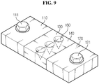
- FIG. 9 is a schematic perspective view showing a shunt resistor according to further another embodiment of the present disclosure.
- first connection element 130 and the second connection element 140 may be configured such that one surface of the first connection element 130 contacts one surface of the second connection element 140.
- first connection element 130 and the second connection element 140 may be integrally formed.
- the shunt resistor 100 may have a concave portion 160 perpendicular to the lengthwise direction at the center where the first connection element 130 and the second connection element 140 contact.
- the concave portion 160 may be formed between the first connection element 130 and the second connection element 140.
- an empty space may be formed between the first connection element 130 and the second connection element 140.
- the first connection element 130 and the second connection element 140 may be distinguished each other around the area where the concave portion 160 is formed.
- the shunt resistor 100 may further include a resistor block 170.
- the resistor block 170 may be configured to be inserted into the concave portion 160.
- the resistor block 170 may be formed to match the shape of the concave portion 160 and inserted into the concave portion 160.
- the resistor block 170 may be made of an electrically conductive material. In this case, the current may flow between the first connection element 130 and the second connection element 140 through the resistor block 170.
- the concave portion 160 may be formed in a conic shape.
- the resistor block 170 may be formed in a conic shape to match the shape of the concave portion 160.
- the resistor block 170 may have a plurality of conic shapes in different sizes.
- the resistor block 170 may be configured to be detachable from the concave portion 160.
- FIG. 8 are schematic cross-sectional views showing that the resistor blocks 170 of conic shapes in different sizes are inserted into the concave portions 160.
- the shape of the concave portion 160 and the resistor block 170 is not limited to the conic shape, and the concave portion 160 and the resistor block 170 may be formed in various shapes, for example, cylinders, rectangular prisms or square or rectangular pyramids.
- the area of indirect contact between the first connection element 130 and the second connection element 140 is smaller than those of (b) and (c), and thus the resistance value between the first connection terminal 111 and the second connection terminal 121 may be higher.
- the area of indirect contact between the first connection element 130 and the second connection element 140 is larger than those of (a) and (b), and thus the resistance value between the first connection terminal 111 and the second connection terminal 121 may be lower.
- the shunt resistor 100 may have a plurality of concave portions 160.
- the plurality of concave portions 160 may be formed between the first connection element 130 and the second connection element 140, and the resistor block 170 may be selectively inserted into the plurality of concave portions 160.
- the resistance value between the first connection element 130 and the second connection element 140 may be adjusted by adjusting the number or size of the resistor block 170 inserted into the plurality of concave portions 160.
- the shunt resistor 100 may accurately detect the flow of current by decreasing or increasing the resistance value of the shunt resistor 100 very precisely through adjustment of the size or the number of inserted resistor blocks 170.
- 'unit' such as 'detection unit' is used herein, it refers to a logical component unit, and it is obvious to those skilled in the art that the term does not necessarily indicate a component that may or should be physically separated.
Abstract
Description
- The present application claims the benefit of Korean Patent Application No.
10-2018-0035972 filed on March 28, 2018 - The present disclosure relates to a shunt resistor and an apparatus for detecting current including the same, and more particularly, to an improved shunt resistor for enhancing accuracy of current detection in the process of detecting current flowing through the shunt resistor and an apparatus for detecting current including the same.
- Recently, there is dramatically growing demand for portable electronic products such as laptop computers, video cameras and mobile phones, and with the extensive development of accumulators for energy storage, robots and satellites, many studies are being made on high performance secondary batteries that can be recharged repeatedly.
- Currently, commercially available secondary batteries include nickel-cadmium batteries, nickel-hydrogen batteries, nickel-zinc batteries, lithium secondary batteries and the like, and among them, lithium secondary batteries have little or no memory effect, and thus they are gaining more attention than nickel-based secondary batteries for their advantages of free charging and discharging, a very low self-discharge rate and high energy density.
- Batteries are used in a wide range of applications, and in many cases, large capacity is required in commercial applications in which batteries are widely used in recent years, such as electric-drive vehicles or smart grid systems. To increase the capacity of battery packs, there may be a method that increases the capacity of secondary batteries or battery cells themselves, but in this case, the capacity increase effect is not so large, and there is a physical limitation on the size expansion of the secondary batteries, and another disadvantage is inconvenient management. Accordingly, generally, a battery pack including battery modules connected in series and in parallel is widely used.
- When secondary batteries are used in the form of an assembly, for example, the unit secondary batteries may be swollen and damaged by overheat in the event that maloperation occurs due to a flow of overcurrent. Accordingly, it is necessary to always measure and monitor the state values of each unit secondary battery such as voltage and temperature in order to prevent each unit secondary battery from being overcharged or overdischarged.
- Conventionally, the state of the battery pack is diagnosed by installing a voltage measuring shunt resistor at a component included in the battery pack such as a bus bar, and calculating the current flowing through the shunt resistor based on the measured voltage value. However, when shunt resistors and measurement devices are used to obtain measured values with high reliability, the number of busbars increases, and the battery pack increases in volume and price. The volume increase of the battery pack has an adverse influence on high efficiency and high energy density.
- Accordingly, because it is necessary to reduce the size of the battery pack in order to improve the efficiency and energy density of the battery pack, there is a need to improve reliability of voltage and current measurement of the shunt resistor.
- The present disclosure is designed under the background of the conventional art described above, and therefore, the present disclosure is directed to providing an improved shunt resistor for enhancing accuracy of current detection in the process of detecting current flowing through the shunt resistor and an apparatus for detecting current including the same.
- These and other objects and advantages of the present disclosure will be understood by the following description and will be apparent from the embodiments of the present disclosure. Further, it will be readily understood that the objects and advantages of the present disclosure can be realized by the means set forth in the appended claims and combinations thereof.
- To achieve the above-described object, a shunt resistor according to an embodiment of the present disclosure includes two busbars made of an electrically conductive material and spaced apart a predetermined distance, a first connection element made of an electrically conductive material and configured to be mounted in a first busbar provided on one side among the two busbars, and a second connection element made of an electrically conductive material and configured to be mounted in a second busbar provided on the other side among the two busbars, wherein the first connection element and the second connection element are configured to have an increase or decrease in an area of direct or indirect contact between the first connection element and the second connection element.
- Additionally, the first connection element may include a first interlock that protrudes perpendicular to a lengthwise direction from the first busbar toward the second busbar and is formed in a shape of teeth, the second connection element may include a second interlock that protrudes perpendicular to a lengthwise direction from the second busbar toward the first busbar and is formed in a shape of teeth, and the first connection element and the second connection element may be configured to directly contact each other when the first interlock and the second interlock are engaged with each other.
- Additionally, the first interlock may be formed of the teeth protruding upwards, the second interlock may be formed of the teeth protruding downwards, and the teeth of the first interlock and the second interlock may have matching shapes.
- Additionally, the shunt resistor according to an embodiment of the present disclosure may be configured to have an increase or decrease in an area of engagement between the first interlock and the second interlock as the first connection element and the second connection element move in the lengthwise direction when the first interlock and the second interlock are engaged with each other.
- Additionally, in the shunt resistor according to an embodiment of the present disclosure, at least two teeth may be provided in each of the first interlock and the second interlock, and as the number of engaged teeth changes, the area of engagement between the first interlock and the second interlock may increase or decrease.
- Additionally, the first connection element and the second connection element may include a plurality of protrusion portions which is spaced apart from each other and protrudes in a direction facing each other, the plurality of protrusion portions may be spaced apart in a vertical direction, and the shunt resistor according to an embodiment of the present disclosure may further include at least one resistor bar which is mounted between the first connection element and the second connection element, wherein the at least one resistor bar may be formed in a shape of a plate, with one side mounted between two protrusion portions provided in the first connection element, and the other side mounted between two protrusion portions provided in the second connection element.
- Additionally, the at least one resistor bar may be configured to be detachable from the first connection element and the second connection element.
- Additionally, the first connection element and the second connection element may be configured such that one surface of the first connection element contacts one surface of the second connection element, and may have a concave portion perpendicular to the lengthwise direction at a center where the first connection element and the second connection element contact, and the shunt resistor according to an embodiment of the present disclosure may further include a resistor block configured to be inserted into the concave portion.
- Additionally, the concave portion may be formed in a conic shape, and the resistor block may be formed in a plurality of conic shapes in different sizes, and configured to be detachable from the concave portion.
- In addition, to achieve the above-described object, an apparatus for detecting current according to an embodiment of the present disclosure includes two busbars made of an electrically conductive material and spaced apart a predetermined distance, a first connection element made of an electrically conductive material and configured to be mounted in a first busbar provided on one side among the two busbars, a second connection element made of an electrically conductive material and configured to be mounted in a second busbar provided on the other side among the two busbars, and a detection unit electrically connected to the first connection element and the second connection element, and configured to detect current flowing between the two busbars using voltage applied between the first connection element and the second connection element, wherein the first connection element and the second connection element may be configured to have an increase or decrease in an area of direct or indirect contact between the first connection element and the second connection element.
- In addition, to achieve the above-described object, a battery pack according to an embodiment of the present disclosure includes the apparatus for detecting current according to the present disclosure.
- According to an aspect of the present disclosure, the resistance value of the shunt resistor may be decreased or increased. Additionally, a plurality of resistor bars or resistor blocks having various shapes may be provided to make fine adjustments of the resistance value of the shunt resistor.
- Particularly, it is possible to detect the current flowing through the shunt resistor by adjusting the resistance value of the shunt resistor conveniently and accurately through selection of the number of resistor bars or resistor blocks.
- The present disclosure may have a variety of other effects, and these and other effects can be understood by the following description and will be apparent from the embodiments of the present disclosure.
- The accompanying drawings illustrate a preferred embodiment of the present disclosure, and together with the following detailed description of the present disclosure, serve to provide a further understanding of the technical aspects of the present disclosure, and thus the present disclosure should not be construed as limited to the drawings.
-
FIG. 1 is a schematic diagram showing an apparatus for detecting current connected to components of a battery pack according to an embodiment of the present disclosure. -
FIG. 2 is a schematic perspective view showing a shunt resistor according to an embodiment of the present disclosure. -
FIG. 3 is an exploded perspective view of a shunt resistor according to another embodiment of the present disclosure. -
FIG. 4 is an assembled perspective view of the shunt resistor ofFIG. 3 . -
FIG. 5 is an exploded perspective view of a shunt resistor according to still another embodiment of the present disclosure. -
FIG. 6 is an assembled perspective view showing a resistor bar additionally coupled to the shunt resistor ofFIG. 5 . -
FIG. 7 is a schematic perspective view showing a shunt resistor according to yet another embodiment of the present disclosure. -
FIG. 8 is a schematic cross-sectional view showing different resistor blocks inserted into the shunt resistor ofFIG. 7 . -
FIG. 9 is a schematic perspective view showing a shunt resistor according to further another embodiment of the present disclosure. - Hereinafter, the preferred embodiments of the present disclosure will be described in detail with reference to the accompanying drawings. Prior to the description, it should be understood that the terms or words used in the specification and the appended claims should not be construed as being limited to general and dictionary meanings, but interpreted based on the meanings and concepts corresponding to the technical aspects of the present disclosure on the basis of the principle that the inventor is allowed to define the terms appropriately for the best explanation.
- Therefore, the embodiments described herein and illustrations shown in the drawings are just a most preferred embodiment of the present disclosure, but not intended to fully describe the technical aspects of the present disclosure, so it should be understood that a variety of other equivalents and modifications could be made thereto at the time of filing the application.
- Additionally, in describing the present disclosure, when it is deemed that a certain detailed description of relevant known elements or functions renders the key subject matter of the present disclosure ambiguous, the detailed description is omitted herein.
- Unless the context clearly indicates otherwise, it will be understood that the term "comprises" or "includes" when used in this specification, specifies the presence of stated elements, but does not preclude the presence or addition of one or more other elements. Additionally, the term 'detection unit' as used herein refers to a processing unit of at least one function or operation, and this may be implemented by hardware or software alone or in combination.
- In addition, throughout the specification, it will be further understood that when an element is referred to as being "connected to" another element, it can be directly connected to the other element or intervening elements may be present.
-
FIG. 1 is a schematic diagram showing an apparatus for detecting current connected to components of a battery pack according to an embodiment of the present disclosure, andFIG. 2 is a schematic perspective view showing a shunt resistor according to an embodiment of the present disclosure. - Referring to
FIGS. 1 and2 , theshunt resistor 100 according to an embodiment of the present disclosure may be provided in abattery pack 1 in itself. That is, thebattery pack 1 according to the present disclosure may include theshunt resistor 100 or the apparatus for detecting current according to the present disclosure as described below. Here, thebattery pack 1 may include at least onesecondary battery 10, theshunt resistor 100, the apparatus for detecting current, electrical equipment (BMS, relays, fuses, etc.) and a case. - For example, as shown in the configuration of
FIG. 1 , theshunt resistor 100 according to the present disclosure may be provided in thebattery pack 1. Additionally, theshunt resistor 100 may be electrically connected to one terminal of thesecondary battery 10. Additionally, two terminals of theshunt resistor 100 may be electrically connected to adetection unit 200. Here, the apparatus for detecting current according to the present disclosure may include theshunt resistor 100 and thedetection unit 200. In more detail, the charge/discharge current flowing between the positive terminal of thebattery pack 1 and the positive terminal of thesecondary battery 10 may flow through theshunt resistor 100. Additionally, thedetection unit 200 may detect an amount of current flowing through theshunt resistor 100 by measuring the voltage across the two terminals of theshunt resistor 100. - The
shunt resistor 100 according to an embodiment of the present disclosure includes two busbars, afirst connection element 130 and asecond connection element 140. - The two busbars may be made of an electrically conductive material. Through this configuration, current can flow in the two busbars. Additionally, the two busbars may be spaced apart a predetermined distance. Here, the two busbars may include a
first busbar 110 provided on one side and asecond busbar 120 provided on the other side. For example, as shown in the configuration ofFIG. 2 , thefirst busbar 110 and thesecond busbar 120 may be spaced apart a predetermined distance in a lengthwise direction on the same plane. Here, the lengthwise direction is a direction from thefirst busbar 110 toward thefirst connection element 130, and thesecond connection element 140 and thesecond busbar 120 may be disposed from thefirst busbar 110 toward the lengthwise direction. For example, referring toFIG. 2 , the lengthwise direction may include a direction of an imaginary extension line connecting afirst connection terminal 111 and asecond connection terminal 121. - Preferably, as shown in the configuration of
FIG. 2 , thefirst busbar 110 and thesecond busbar 120 may include thefirst connection terminal 111 and thesecond connection terminal 121. For example, thefirst connection terminal 111 and thesecond connection terminal 121 may be electrically connected to thedetection unit 200. - The
first connection element 130 may be made of an electrically conductive material. Additionally, thefirst connection element 130 may be configured to be mounted in thefirst busbar 110 provided on one side among the two busbars. For example, as shown in the configuration ofFIG. 2 , thefirst connection element 130 may be provided between thefirst busbar 110 and thesecond busbar 120 to determine the resistance value between thefirst busbar 110 and thesecond busbar 120. Preferably, thefirst connection element 130 and thefirst busbar 110 may be integrally formed as shown in the configuration ofFIG. 2 . That is, thefirst connection element 130 and thefirst busbar 110 may be integrally formed with the upper and lower surfaces arranged in parallel on the same plane. - The
second connection element 140 may be made of an electrically conductive material. Additionally, thesecond connection element 140 may be configured to be mounted in thesecond busbar 120 provided on the other side among the two busbars. For example, as shown in the configuration ofFIG. 2 , thesecond connection element 140 may be provided between thefirst busbar 110 and thesecond busbar 120 to determine the resistance value between thefirst busbar 110 and thesecond busbar 120. Preferably, thesecond connection element 140 and thesecond busbar 120 may be integrally formed as shown in the configuration ofFIG. 2 . That is, thesecond connection element 140 and thesecond busbar 120 may be integrally formed with the upper and lower surfaces arranged in parallel on the same plane. - Additionally, one surface of the
first connection element 130 may contact one surface of thesecond connection element 140 as shown in the configuration ofFIG. 2 . For example, thefirst connection element 130 and thesecond connection element 140 may be integrally formed. - Particularly, the
first connection element 130 and thesecond connection element 140 may be configured to have an increase or decrease in the area of indirect or direct contact between thefirst connection element 130 and thesecond connection element 140. In more detail, to detect the current in theshunt resistor 100 according to the present disclosure, the voltage across the two terminals of theshunt resistor 100 is measured, and in this instance, in the configuration ofFIG. 2 , voltage measured between thefirst connection terminal 111 and thesecond connection terminal 121 may be used as the voltage across the two terminals of theshunt resistor 100. In this case, thefirst connection element 130 and thesecond connection element 140 may determine the resistance value between thefirst connection terminal 111 and thesecond connection terminal 121 according to the material or shape of thefirst connection element 130 and thesecond connection element 140. - For example, the
first connection element 130 and thesecond connection element 140 may contact each other directly or indirectly. In this case, when thefirst connection element 130 and thesecond connection element 140 contact each other without intervention, this is the case in which thefirst connection element 130 and thesecond connection element 140 directly contact each other, and when any other component of an electrically conductive material is inserted between thefirst connection element 130 and thesecond connection element 140, this is the case in which thefirst connection element 130 and thesecond connection element 140 indirectly contact each other. - Additionally, when the area of contact between the
first connection element 130 and thesecond connection element 140 increases, the resistance value between thefirst connection terminal 111 and thesecond connection terminal 121 may decrease. On the contrary, when the area of contact between thefirst connection element 130 and thesecond connection element 140 decreases, the resistance value between thefirst connection terminal 111 and thesecond connection terminal 121 may increase. - Through this configuration, the
shunt resistor 100 according to the present disclosure may accurately detect the flow of current by decreasing or increasing the resistance value of theshunt resistor 100 very precisely. - The apparatus for detecting current according to an embodiment of the present disclosure includes two busbars, a
first connection element 130, asecond connection element 140 and adetection unit 200. A description of the two busbars, thefirst connection element 130 and thesecond connection element 140 overlaps the above description of theshunt resistor 100 and is omitted herein. - As shown in the configuration of
FIG. 1 , thedetection unit 200 may be electrically connected to the two terminals of theshunt resistor 100. In more detail, thedetection unit 200 may be electrically connected to thefirst connection element 130 and thesecond connection element 140. Alternatively, thedetection unit 200 may be electrically connected to thefirst connection terminal 111 and thesecond connection terminal 121. Additionally, thedetection unit 200 may detect the current flowing through theshunt resistor 100 using the voltage measured from the two terminals of theshunt resistor 100. In more detail, thedetection unit 200 may detect the current flowing between the two busbars using the voltage applied between thefirst connection element 130 and thesecond connection element 140. - In this configuration, at least some components of the apparatus for detecting current according to the present disclosure may be implemented by supplementing or adding the functions of the components conventionally included in the battery. For example, the detection unit of the apparatus for detecting current according to the present disclosure may be implemented by a Battery Management System (BMS) provided in the battery pack. Here, the battery may be a concept that encompasses the battery module or the battery pack.
-
FIG. 3 is an exploded perspective view of a shunt resistor according to another embodiment of the present disclosure, andFIG. 4 is an assembled perspective view of the shunt resistor ofFIG. 3 . - Referring to
FIGS. 3 and4 , thefirst connection element 130 according to an embodiment of the present disclosure may include a first interlock. Additionally, thesecond connection element 140 may include a second interlock. - The first interlock may protrude perpendicular to the lengthwise direction from the
first busbar 110 toward thesecond busbar 120 and may be formed in the shape of teeth. Additionally, the second interlock may protrude perpendicular to the lengthwise direction from thesecond busbar 120 toward thefirst busbar 110, and may be formed in the shape of teeth. Particularly, thefirst connection element 130 and thesecond connection element 140 may be configured to directly contact when the first interlock and the second interlock are engaged with each other. - Preferably, as shown in the configuration of
FIG. 3 , the first interlock according to an embodiment of the present disclosure may have the teeth protruding upwards. Additionally, the second interlock may have the teeth protruding downwards. Particularly, the first interlock and the second interlock may have the teeth in shapes that match each other. As opposed to the configuration shown inFIG. 3 , the teeth of the first interlock may protrude downwards and the teeth of the second interlock may protrude upwards, and the first interlock and the second interlock may be engaged with each other. Additionally, the teeth of the first interlock and the teeth of the second interlock may protrude in a diagonal or horizontal direction that is perpendicular to the lengthwise direction, and may be engaged with each other. - In more detail, the teeth provided in the first interlock and the second interlock have shapes that match each other, so when the first interlock and the second interlock are engaged with each other, as shown in the configuration of
FIG. 4 , theshunt resistor 100 according to an embodiment of the present disclosure may be configured to have no empty space at the area where the first interlock and the second interlock meet each other. That is, according to an embodiment of the present disclosure, when the first interlock and the second interlock are engaged with each other, the first interlock and the second interlock are in close contact with each other, thereby minimizing a resistance loss resulting from spacing, and improving the reliability of voltage and current measurement of theshunt resistor 100. - Additionally, preferably, when the first interlock and the second interlock are engaged with each other, the
shunt resistor 100 according to an embodiment of the present disclosure may have an increase or decrease in the area of engagement between the first interlock and the second interlock as thefirst connection element 130 and thesecond connection element 140 moves in the lengthwise direction. In more detail, as shown in the configuration ofFIG. 3 , the first interlock and the second interlock may be detachable. Additionally, the first interlock and the second interlock may be configured to have an increase or decrease in the area of engagement between the first interlock and the second interlock according to the number of engaged teeth. - Particularly, at least two teeth may be provided in each of the first interlock and the second interlock. For example, in the configuration of
FIGS. 3 and4 , each of the first interlock and the second interlock has three teeth. Additionally, theshunt resistor 100 according to an embodiment of the present disclosure may be configured to have an increase or decrease in the area of engagement between the first interlock and the second interlock with the changes in the number of engaged teeth. For example, the first interlock and the second interlock may have single engagement where each one tooth is engaged. Additionally, the first interlock and the second interlock may have double engagement where each two teeth are engaged. - Through this configuration, the
shunt resistor 100 according to the present disclosure may accurately detect the flow of current by decreasing or increasing the resistance value of theshunt resistor 100 very precisely through adjustment of the number of engaged teeth. -
FIG. 5 is an exploded perspective view of a shunt resistor according to still another embodiment of the present disclosure, andFIG. 6 is an assembled perspective view showing a resistor bar additionally coupled to the shunt resistor ofFIG. 5 . - Referring to
FIGS. 5 and6 , thefirst connection element 130 and thesecond connection element 140 according to an embodiment of the present disclosure may be spaced apart from each other. Additionally, thefirst connection element 130 and thesecond connection element 140 may have protrusion portion. For example, as shown in the configuration ofFIG. 5 , thefirst connection element 130 and thesecond connection element 140 may have a plurality of protrusion portions that protrudes in directions facing each other. In this case, the plurality of protrusion portions may be spaced apart from each other in the vertical direction. In more detail, thefirst connection element 130 may have a plurality offirst protrusion portions 131 that protrude in a direction facing thesecond connection element 140. Additionally, thesecond connection element 140 may have a plurality ofsecond protrusion portions 141 that protrude in a direction facing thefirst connection element 130. Particularly, the plurality of protrusion portions may be spaced apart in parallel. Additionally, the plurality of protrusion portions may be formed in the shape of a plate with an internal space between two protrusion portions. Theshunt resistor 100 according to an embodiment of the present disclosure may further include at least oneresistor bar 150. The at least oneresistor bar 150 may be configured to be mounted between thefirst connection element 130 and thesecond connection element 140. In more detail, the at least oneresistor bar 150 may be formed in the shape of a plate, with one side mounted between two protrusion portions provided in thefirst connection element 130, and the other side mounted between two protrusion portions provided in thesecond connection element 140. For example, as shown in the configuration ofFIG. 5 , theresistor bar 150 may be mounted between thefirst connection element 130 and thesecond connection element 140 to indirectly connect thefirst connection element 130 and thesecond connection element 140. Additionally, theresistor bar 150 may be made of an electrically conductive material. In this case, the current may flow between thefirst connection element 130 and thesecond connection element 140 through theresistor bar 150. - However, the direction in which the plurality of protrusion portions is spaced apart is not limited to the vertical direction shown in
FIGS. 5 and6 , and the plurality of protrusion portions may be spaced apart in the horizontal or diagonal direction. That is, the plurality of protrusion portions provided in thefirst connection element 130 may be spaced apart in a direction perpendicular to the direction (the lengthwise direction) facing thesecond connection element 140. Likewise, the plurality of protrusion portions provided in thesecond connection element 140 may be spaced apart in a direction perpendicular to the direction (the lengthwise direction) facing thefirst connection element 130. For example, in addition to the vertical direction shown inFIGS. 5 and6 , the plurality of protrusion portions provided in thefirst connection element 130 and the plurality of protrusion portions provided in thesecond connection element 140 may be spaced apart in the horizontal direction that is perpendicular to the lengthwise direction. In this case, theresistor bar 150 may be mounted between the protrusion portions provided in thefirst connection element 130 and thesecond connection element 140 while standing by 90° rotation around the dashed line shown in the shape shown inFIG. 5 as a rotation axis. That is, thefirst connection element 130 and thesecond connection element 140 have the protrusion portions, and may be indirectly connected through theresistor bar 150 mounted between the protrusion portions. - Additionally, in addition to the vertical direction shown in
FIGS. 5 and6 , the plurality of protrusion portions provided in thefirst connection element 130 and the plurality of protrusion portions provided in thesecond connection element 140 may be spaced apart in the diagonal direction that is perpendicular to the lengthwise direction. In this case, theresistor bar 150 may be mounted between the protrusion portions provided in thefirst connection element 130 and thesecond connection element 140 by clockwise or counterclockwise rotation around the dashed line shown in the shape shown inFIG. 5 as a rotation axis. In this instance, each of the plurality ofresistor bars 150 mounted between thefirst connection element 130 and thesecond connection element 140 may be formed to match the size and shape of the protrusion portions of thefirst connection element 130 and thesecond connection element 140 where the resistor bars 150 are mounted, and the size of each of the plurality of resistor bars 150 may be different. - Preferably, the resistor bars 150 may be inserted in parallel at a predetermined interval between the
first connection element 130 and thesecond connection element 140. In this case, the protrusion portions provided in thefirst connection element 130 and thesecond connection element 140 may be formed in heights that match each other. Additionally, the plurality of protrusion portions may be formed in parallel. - Additionally, preferably, the at least one
resistor bar 150 may be configured to be detachable from thefirst connection element 130 and thesecond connection element 140. Particularly, theshunt resistor 100 according to an embodiment of the present disclosure may be configured to have a decrease or increase in the area of indirect contact between thefirst connection element 130 and thesecond connection element 140 with the decreasing or increasing number ofresistor bars 150 mounted between thefirst connection element 130 and thesecond connection element 140. For example, as shown in the configuration ofFIG. 6 , the plurality of resistor bars 150 may be mounted in the plurality of protrusion portions provided in thefirst connection element 130 and thesecond connection element 140. - Through this configuration, the
shunt resistor 100 according to the present disclosure may accurately detect the flow of current by decreasing or increasing the resistance value of theshunt resistor 100 very precisely through adjustment of the number of mounted resistor bars 150. -
FIG. 7 is a schematic perspective view showing a shunt resistor according to yet another embodiment of the present disclosure, andFIG. 8 is a schematic cross-sectional view showing different resistor blocks inserted into the shunt resistor ofFIG. 7 . Additionally,FIG. 9 is a schematic perspective view showing a shunt resistor according to further another embodiment of the present disclosure. - Referring to
FIGS. 7 to 9 , thefirst connection element 130 and thesecond connection element 140 according to an embodiment of the present disclosure may be configured such that one surface of thefirst connection element 130 contacts one surface of thesecond connection element 140. Alternatively, thefirst connection element 130 and thesecond connection element 140 may be integrally formed. - Additionally, the
shunt resistor 100 according to an embodiment of the present disclosure may have aconcave portion 160 perpendicular to the lengthwise direction at the center where thefirst connection element 130 and thesecond connection element 140 contact. For example, as shown in the configuration ofFIG. 7 , theconcave portion 160 may be formed between thefirst connection element 130 and thesecond connection element 140. In this case, an empty space may be formed between thefirst connection element 130 and thesecond connection element 140. Additionally, when thefirst connection element 130 and thesecond connection element 140 are integrally formed, thefirst connection element 130 and thesecond connection element 140 may be distinguished each other around the area where theconcave portion 160 is formed. - Preferably, the
shunt resistor 100 according to an embodiment of the present disclosure may further include aresistor block 170. Theresistor block 170 may be configured to be inserted into theconcave portion 160. In more detail, theresistor block 170 may be formed to match the shape of theconcave portion 160 and inserted into theconcave portion 160. Additionally, theresistor block 170 may be made of an electrically conductive material. In this case, the current may flow between thefirst connection element 130 and thesecond connection element 140 through theresistor block 170. - In more detail, as shown in the configuration of
FIG. 7 , theconcave portion 160 may be formed in a conic shape. Additionally, theresistor block 170 may be formed in a conic shape to match the shape of theconcave portion 160. - More preferably, the
resistor block 170 according to an embodiment of the present disclosure may have a plurality of conic shapes in different sizes. In this case, theresistor block 170 may be configured to be detachable from theconcave portion 160. For example, (a), (b) and (c) ofFIG. 8 are schematic cross-sectional views showing that the resistor blocks 170 of conic shapes in different sizes are inserted into theconcave portions 160. However, the shape of theconcave portion 160 and theresistor block 170 is not limited to the conic shape, and theconcave portion 160 and theresistor block 170 may be formed in various shapes, for example, cylinders, rectangular prisms or square or rectangular pyramids. - In (a), (b) and (c) of
FIG. 8 , on the basis of the shape of theconcave portion 160, (a) shows that theresistor block 170 of the smallest size is inserted into theconcave portion 160, (b) shows that theresistor block 170 of the intermediate size is inserted into theconcave portion 160, and (c) shows that theresistor block 170 of the largest size is inserted into theconcave portion 160. In the case of (c), the size of theresistor block 170 may match the size of theconcave portion 160. - In more detail, in the case of (a), the area of indirect contact between the
first connection element 130 and thesecond connection element 140 is smaller than those of (b) and (c), and thus the resistance value between thefirst connection terminal 111 and thesecond connection terminal 121 may be higher. On the contrary, in the case of (c), the area of indirect contact between thefirst connection element 130 and thesecond connection element 140 is larger than those of (a) and (b), and thus the resistance value between thefirst connection terminal 111 and thesecond connection terminal 121 may be lower. - Additionally, the
shunt resistor 100 according to an embodiment of the present disclosure may have a plurality ofconcave portions 160. For example, as shown in the configuration ofFIG. 9 , the plurality ofconcave portions 160 may be formed between thefirst connection element 130 and thesecond connection element 140, and theresistor block 170 may be selectively inserted into the plurality ofconcave portions 160. In more detail, the resistance value between thefirst connection element 130 and thesecond connection element 140 may be adjusted by adjusting the number or size of theresistor block 170 inserted into the plurality ofconcave portions 160. - Through this configuration, the
shunt resistor 100 according to the present disclosure may accurately detect the flow of current by decreasing or increasing the resistance value of theshunt resistor 100 very precisely through adjustment of the size or the number of inserted resistor blocks 170. - Meanwhile, the terms importing directions such as up, down, left, right, front and rear are used herein, but this is provided for convenience of description only, and it is obvious to those skilled in the art that the terms may change depending on the position of the stated element or an observer.
- While the present disclosure has been hereinabove described with regard to a limited number of embodiments and drawings, the present disclosure is not limited thereto and various modifications and changes may be made by those skilled in the art within the technical aspects of the present disclosure and the equivalent scope of the appended claims.
- Although the term 'unit' such as 'detection unit' is used herein, it refers to a logical component unit, and it is obvious to those skilled in the art that the term does not necessarily indicate a component that may or should be physically separated.
-
- 1:
- Battery pack
- 10:
- Secondary battery
- 100:
- Shunt resistor
- 110:
- First busbar
- 111:
- First connection terminal
- 120:
- Second busbar
- 121:
- Second connection terminal
- 130:
- First connection element
- 131:
- First protrusion portion
- 140:
- Second connection element
- 141:
- Second protrusion portion
- 150:
- Resistor bar
- 160:
- Concave portion
- 170:
- Resistor block
- 200:
- Detection unit
Claims (11)
- A shunt resistor comprising:two busbars made of an electrically conductive material, and spaced apart a predetermined distance;a first connection element made of an electrically conductive material, and configured to be mounted in a first busbar provided on one side among the two busbars; anda second connection element made of an electrically conductive material, and configured to be mounted in a second busbar provided on the other side among the two busbars,wherein the first connection element and the second connection element are configured to have an increase or decrease in an area of direct or indirect contact between the first connection element and the second connection element.
- The shunt resistor according to claim 1, wherein the first connection element includes a first interlock that protrudes perpendicular to a lengthwise direction from the first busbar toward the second busbar and is formed in a shape of teeth,
the second connection element includes a second interlock that protrudes perpendicular to a lengthwise direction from the second busbar toward the first busbar and is formed in a shape of teeth, and
the first connection element and the second connection element are configured to directly contact each other when the first interlock and the second interlock are engaged with each other. - The shunt resistor according to claim 2, wherein the first interlock is formed of the teeth protruding upwards,
the second interlock is formed of the teeth protruding downwards, and
the teeth of the first interlock and the second interlock have matching shapes. - The shunt resistor according to claim 2, wherein when the first interlock and the second interlock are engaged with each other, an area of engagement between the first interlock and the second interlock increases or decreases as the first connection element and the second connection element move in the lengthwise direction.
- The shunt resistor according to claim 4, wherein at least two teeth are provided in each of the first interlock and the second interlock, and as the number of engaged teeth changes, the area of engagement between the first interlock and the second interlock increases or decreases.
- The shunt resistor according to claim 1, wherein the first connection element and the second connection element include a plurality of protrusion portions which is spaced apart from each other and protrudes in a direction facing each other, and the plurality of protrusion portions is spaced apart in a vertical direction, and
the shunt resistor further comprises:at least one resistor bar which is mounted between the first connection element and the second connection element,wherein the at least one resistor bar is formed in a shape of a plate, with one side mounted between two protrusion portions provided in the first connection element, and the other side mounted between two protrusion portions provided in the second connection element. - The shunt resistor according to claim 6, wherein the at least one resistor bar is configured to be detachable from the first connection element and the second connection element.
- The shunt resistor according to claim 1, wherein the first connection element and the second connection element are configured such that one surface of the first connection element contacts one surface of the second connection element, and have a concave portion perpendicular to the lengthwise direction at a center where the first connection element and the second connection element contact, and
the shunt resistor further comprises:
a resistor block configured to be inserted into the concave portion. - The shunt resistor according to claim 8, wherein the concave portion is formed in a conic shape, and
the resistor block is formed in a plurality of conic shapes in different sizes, and is configured to be detachable from the concave portion. - An apparatus for detecting current, comprising:two busbars made of an electrically conductive material, and spaced apart a predetermined distance;a first connection element made of an electrically conductive material, and configured to be mounted in a first busbar provided on one side among the two busbars;a second connection element made of an electrically conductive material, and configured to be mounted in a second busbar provided on the other side among the two busbars; anda detection unit electrically connected to the first connection element and the second connection element, and configured to detect current flowing between the two busbars using voltage applied between the first connection element and the second connection element,wherein the first connection element and the second connection element are configured to have an increase or decrease in an area of direct or indirect contact between the first connection element and the second connection element.
- A battery pack comprising the apparatus for detecting current according to claim 10.
Applications Claiming Priority (2)
| Application Number | Priority Date | Filing Date | Title |
|---|---|---|---|
| KR1020180035972A KR102312445B1 (en) | 2018-03-28 | 2018-03-28 | Shunt resistor and apparatus for detecting current including the same |
| PCT/KR2019/003452 WO2019190144A1 (en) | 2018-03-28 | 2019-03-25 | Shunt resistor and current detecting device including same |
Publications (3)
| Publication Number | Publication Date |
|---|---|
| EP3674716A1 true EP3674716A1 (en) | 2020-07-01 |
| EP3674716A4 EP3674716A4 (en) | 2021-01-27 |
| EP3674716B1 EP3674716B1 (en) | 2023-06-14 |
Family
ID=68059318
Family Applications (1)
| Application Number | Title | Priority Date | Filing Date |
|---|---|---|---|
| EP19778075.2A Active EP3674716B1 (en) | 2018-03-28 | 2019-03-25 | Shunt resistor and apparatus for detecting current including the same |
Country Status (6)
| Country | Link |
|---|---|
| US (1) | US11320490B2 (en) |
| EP (1) | EP3674716B1 (en) |
| JP (1) | JP7004226B2 (en) |
| KR (1) | KR102312445B1 (en) |
| CN (1) | CN111133321B (en) |
| WO (1) | WO2019190144A1 (en) |
Cited By (1)
| Publication number | Priority date | Publication date | Assignee | Title |
|---|---|---|---|---|
| EP4012727A3 (en) * | 2020-12-10 | 2022-10-12 | Wieland-Werke AG | Measuring resistor, resistor assembly and method for the production of same |
Families Citing this family (2)
| Publication number | Priority date | Publication date | Assignee | Title |
|---|---|---|---|---|
| DE102020214083A1 (en) * | 2020-11-10 | 2022-05-12 | Continental Automotive Gmbh | Resistor assembly and battery sensor with resistor assembly |
| JP2023027569A (en) * | 2021-08-17 | 2023-03-02 | 株式会社デンソー | current sensor |
Family Cites Families (27)
| Publication number | Priority date | Publication date | Assignee | Title |
|---|---|---|---|---|
| JPS5092275U (en) * | 1973-12-22 | 1975-08-04 | ||
| JPS59191673U (en) * | 1983-06-07 | 1984-12-19 | 本田技研工業株式会社 | electrical resistor |
| JP2001349907A (en) | 2000-06-07 | 2001-12-21 | Unisia Jecs Corp | Current detector, manufacturing method of resistance in current detector, and method for adjusting resistance in current detector |
| KR100370589B1 (en) | 2000-12-21 | 2003-02-05 | 박현수 | Shunt-intergrated bus bar |
| CN1319078C (en) | 2003-07-09 | 2007-05-30 | 彭德龙 | Precision shunt resistor and manufacturing method thereof |
| CN2634608Y (en) * | 2003-07-09 | 2004-08-18 | 彭德龙 | Precision shunt resistor |
| JP2005136339A (en) * | 2003-10-31 | 2005-05-26 | Fujikura Ltd | Substrate-jointing method and its jointing structure |
| JP4887749B2 (en) * | 2005-11-15 | 2012-02-29 | パナソニック株式会社 | Resistor manufacturing method |
| JP5263733B2 (en) | 2008-04-24 | 2013-08-14 | コーア株式会社 | Metal plate resistor |
| DE102010051007A1 (en) | 2009-12-03 | 2011-06-16 | Koa Corp., Ina-shi | Shunt resistance and manufacturing process therefor |
| WO2012043591A1 (en) * | 2010-09-30 | 2012-04-05 | 三洋電機株式会社 | Power supply device |
| JP5383721B2 (en) | 2011-01-25 | 2014-01-08 | 中国電力株式会社 | Connection structure between conductor ends |
| WO2013005824A1 (en) | 2011-07-07 | 2013-01-10 | コーア株式会社 | Shunt resistor and manufacturing method thereof |
| EP2732295B1 (en) * | 2011-07-14 | 2015-04-29 | Continental Teves AG & Co. oHG | Current measuring device |
| US9054523B2 (en) | 2012-05-25 | 2015-06-09 | Lsis Co., Ltd. | Current detecting mechanism capable of detecting ground fault for direct current circuit breaker |
| JP5545334B2 (en) | 2012-09-13 | 2014-07-09 | ダイキン工業株式会社 | Electronic circuit equipment |
| KR101393104B1 (en) | 2013-05-14 | 2014-05-09 | (주)에이치엔티 | Busbar inverse symetrical type shunt |
| JP6478459B2 (en) * | 2014-02-03 | 2019-03-06 | Koa株式会社 | Resistor and current detection device |
| JP6305816B2 (en) | 2014-04-11 | 2018-04-04 | Koa株式会社 | Metal plate resistor |
| DE102014011593B4 (en) | 2014-08-01 | 2016-05-04 | Isabellenhütte Heusler Gmbh & Co. Kg | Resistance, in particular low-impedance current measuring resistor |
| JP6384211B2 (en) * | 2014-09-03 | 2018-09-05 | 株式会社デンソー | Shunt resistor |
| JP6643859B2 (en) | 2015-10-15 | 2020-02-12 | サンコール株式会社 | Manufacturing method of shunt resistor |
| JP6695122B2 (en) | 2015-10-15 | 2020-05-20 | サンコール株式会社 | Manufacturing method of shunt resistor |
| JP6687462B2 (en) * | 2016-05-19 | 2020-04-22 | サンコール株式会社 | Shunt resistor and shunt type current detector |
| JP6764692B2 (en) * | 2016-05-24 | 2020-10-07 | Koa株式会社 | Shunt resistor and shunt resistor mounting structure |
| KR101998091B1 (en) | 2016-07-29 | 2019-07-09 | 주식회사 엘지화학 | Apparatus for measuring current using shunt resistor |
| KR101869805B1 (en) | 2016-09-29 | 2018-07-24 | 전자부품연구원 | Anode for a lithium secondary battery, method of the same and lithium secondary battery using the same |
-
2018
- 2018-03-28 KR KR1020180035972A patent/KR102312445B1/en active IP Right Grant
-
2019
- 2019-03-25 EP EP19778075.2A patent/EP3674716B1/en active Active
- 2019-03-25 CN CN201980004715.5A patent/CN111133321B/en active Active
- 2019-03-25 US US16/635,403 patent/US11320490B2/en active Active
- 2019-03-25 WO PCT/KR2019/003452 patent/WO2019190144A1/en unknown
- 2019-03-25 JP JP2020501821A patent/JP7004226B2/en active Active
Cited By (2)
| Publication number | Priority date | Publication date | Assignee | Title |
|---|---|---|---|---|
| EP4012727A3 (en) * | 2020-12-10 | 2022-10-12 | Wieland-Werke AG | Measuring resistor, resistor assembly and method for the production of same |
| US11621107B2 (en) | 2020-12-10 | 2023-04-04 | Wieland-Werke Ag | Resistor assembly and method for producing same |
Also Published As
| Publication number | Publication date |
|---|---|
| EP3674716B1 (en) | 2023-06-14 |
| JP7004226B2 (en) | 2022-01-21 |
| JP2020528140A (en) | 2020-09-17 |
| KR102312445B1 (en) | 2021-10-12 |
| KR20190113378A (en) | 2019-10-08 |
| CN111133321B (en) | 2022-06-14 |
| EP3674716A4 (en) | 2021-01-27 |
| CN111133321A (en) | 2020-05-08 |
| US11320490B2 (en) | 2022-05-03 |
| WO2019190144A1 (en) | 2019-10-03 |
| US20200182936A1 (en) | 2020-06-11 |
Similar Documents
| Publication | Publication Date | Title |
|---|---|---|
| KR102056875B1 (en) | Battery module and battery pack including the same | |
| CN110710025B (en) | Battery pack with improved assembly structure | |
| EP3674716B1 (en) | Shunt resistor and apparatus for detecting current including the same | |
| CN107210404B (en) | Battery module and battery pack including the same | |
| JP5259599B2 (en) | Battery module interface | |
| US8603663B2 (en) | Battery pack | |
| KR101178152B1 (en) | Battery pack of novel structure | |
| EP3128574A1 (en) | Circuit board for secondary battery and battery pack comprising same | |
| EP3709030B1 (en) | Current detection circuit, battery management system, and battery pack | |
| CN104488114A (en) | Secondary battery, and secondary battery module and secondary battery pack comprising the same | |
| US11480474B2 (en) | Apparatus and method for measuring temperature of battery | |
| CN111630398B (en) | Battery management device, and battery pack and vehicle including the same | |
| EP3609015B1 (en) | Apparatus and method for estimating battery temperature | |
| KR20170050508A (en) | Battery module and battery pack including the same | |
| US11454676B2 (en) | Apparatus for estimating state of secondary battery, and battery pack including the same | |
| KR101802926B1 (en) | Battery having Sensing Assembly Structure for Processing Signal of Cell | |
| US11215669B2 (en) | Apparatus and method for measuring voltage | |
| EP4109662A1 (en) | Battery module, battery pack comprising same, and vehicle | |
| KR20150115251A (en) | Battery module array having 2-cell with center frame type module | |
| KR102447552B1 (en) | Apparatus for detecting state of secondary battery | |
| US11705587B2 (en) | Terminal case having the improved function of estimating state of secondary battery | |
| US9618544B2 (en) | System and method for verifying a reference voltage for battery cell monitoring | |
| KR20210055521A (en) | Battery pack for preventing short circuit | |
| JP2013125683A (en) | Storage battery unit, storage battery module, and connection body |
Legal Events
| Date | Code | Title | Description |
|---|---|---|---|
| STAA | Information on the status of an ep patent application or granted ep patent |
Free format text: STATUS: THE INTERNATIONAL PUBLICATION HAS BEEN MADE |
|
| PUAI | Public reference made under article 153(3) epc to a published international application that has entered the european phase |
Free format text: ORIGINAL CODE: 0009012 |
|
| STAA | Information on the status of an ep patent application or granted ep patent |
Free format text: STATUS: REQUEST FOR EXAMINATION WAS MADE |
|
| 17P | Request for examination filed |
Effective date: 20200323 |
|
| AK | Designated contracting states |
Kind code of ref document: A1 Designated state(s): AL AT BE BG CH CY CZ DE DK EE ES FI FR GB GR HR HU IE IS IT LI LT LU LV MC MK MT NL NO PL PT RO RS SE SI SK SM TR |
|
| AX | Request for extension of the european patent |
Extension state: BA ME |
|
| A4 | Supplementary search report drawn up and despatched |
Effective date: 20210112 |
|
| RIC1 | Information provided on ipc code assigned before grant |
Ipc: H01R 25/14 20060101ALI20201221BHEP Ipc: G01R 15/14 20060101ALI20201221BHEP Ipc: H01C 1/14 20060101ALI20201221BHEP Ipc: H01M 10/48 20060101ALI20201221BHEP Ipc: G01R 31/36 20200101ALI20201221BHEP Ipc: H01M 2/20 20060101ALI20201221BHEP Ipc: G01R 31/382 20190101ALI20201221BHEP Ipc: G01R 1/20 20060101AFI20201221BHEP |
|
| DAV | Request for validation of the european patent (deleted) | ||
| DAX | Request for extension of the european patent (deleted) | ||
| RAP1 | Party data changed (applicant data changed or rights of an application transferred) |
Owner name: LG ENERGY SOLUTION LTD. |
|
| RAP3 | Party data changed (applicant data changed or rights of an application transferred) |
Owner name: LG ENERGY SOLUTION, LTD. |
|
| REG | Reference to a national code |
Ref document number: 602019031094 Country of ref document: DE Ref country code: DE Ref legal event code: R079 Free format text: PREVIOUS MAIN CLASS: G01R0001200000 Ipc: H01M0050500000 |
|
| GRAP | Despatch of communication of intention to grant a patent |
Free format text: ORIGINAL CODE: EPIDOSNIGR1 |
|
| STAA | Information on the status of an ep patent application or granted ep patent |
Free format text: STATUS: GRANT OF PATENT IS INTENDED |
|
| RIC1 | Information provided on ipc code assigned before grant |
Ipc: H01C 1/14 20060101ALI20230222BHEP Ipc: G01R 31/382 20190101ALI20230222BHEP Ipc: G01R 31/36 20060101ALI20230222BHEP Ipc: G01R 15/14 20060101ALI20230222BHEP Ipc: G01R 1/20 20060101ALI20230222BHEP Ipc: H01M 50/583 20210101ALI20230222BHEP Ipc: H01M 50/50 20210101AFI20230222BHEP |
|
| INTG | Intention to grant announced |
Effective date: 20230315 |
|
| GRAS | Grant fee paid |
Free format text: ORIGINAL CODE: EPIDOSNIGR3 |
|
| GRAA | (expected) grant |
Free format text: ORIGINAL CODE: 0009210 |
|
| STAA | Information on the status of an ep patent application or granted ep patent |
Free format text: STATUS: THE PATENT HAS BEEN GRANTED |
|
| AK | Designated contracting states |
Kind code of ref document: B1 Designated state(s): AL AT BE BG CH CY CZ DE DK EE ES FI FR GB GR HR HU IE IS IT LI LT LU LV MC MK MT NL NO PL PT RO RS SE SI SK SM TR |
|
| REG | Reference to a national code |
Ref country code: CH Ref legal event code: EP |
|
| P01 | Opt-out of the competence of the unified patent court (upc) registered |
Effective date: 20230516 |
|
| REG | Reference to a national code |
Ref country code: DE Ref legal event code: R096 Ref document number: 602019031094 Country of ref document: DE |
|
| REG | Reference to a national code |
Ref country code: AT Ref legal event code: REF Ref document number: 1579906 Country of ref document: AT Kind code of ref document: T Effective date: 20230715 |
|
| REG | Reference to a national code |
Ref country code: LT Ref legal event code: MG9D |
|
| REG | Reference to a national code |
Ref country code: NL Ref legal event code: MP Effective date: 20230614 |
|
| PG25 | Lapsed in a contracting state [announced via postgrant information from national office to epo] |
Ref country code: SE Free format text: LAPSE BECAUSE OF FAILURE TO SUBMIT A TRANSLATION OF THE DESCRIPTION OR TO PAY THE FEE WITHIN THE PRESCRIBED TIME-LIMIT Effective date: 20230614 Ref country code: NO Free format text: LAPSE BECAUSE OF FAILURE TO SUBMIT A TRANSLATION OF THE DESCRIPTION OR TO PAY THE FEE WITHIN THE PRESCRIBED TIME-LIMIT Effective date: 20230914 Ref country code: ES Free format text: LAPSE BECAUSE OF FAILURE TO SUBMIT A TRANSLATION OF THE DESCRIPTION OR TO PAY THE FEE WITHIN THE PRESCRIBED TIME-LIMIT Effective date: 20230614 |
|
| REG | Reference to a national code |
Ref country code: AT Ref legal event code: MK05 Ref document number: 1579906 Country of ref document: AT Kind code of ref document: T Effective date: 20230614 |
|
| PG25 | Lapsed in a contracting state [announced via postgrant information from national office to epo] |
Ref country code: RS Free format text: LAPSE BECAUSE OF FAILURE TO SUBMIT A TRANSLATION OF THE DESCRIPTION OR TO PAY THE FEE WITHIN THE PRESCRIBED TIME-LIMIT Effective date: 20230614 Ref country code: NL Free format text: LAPSE BECAUSE OF FAILURE TO SUBMIT A TRANSLATION OF THE DESCRIPTION OR TO PAY THE FEE WITHIN THE PRESCRIBED TIME-LIMIT Effective date: 20230614 Ref country code: LV Free format text: LAPSE BECAUSE OF FAILURE TO SUBMIT A TRANSLATION OF THE DESCRIPTION OR TO PAY THE FEE WITHIN THE PRESCRIBED TIME-LIMIT Effective date: 20230614 Ref country code: LT Free format text: LAPSE BECAUSE OF FAILURE TO SUBMIT A TRANSLATION OF THE DESCRIPTION OR TO PAY THE FEE WITHIN THE PRESCRIBED TIME-LIMIT Effective date: 20230614 Ref country code: HR Free format text: LAPSE BECAUSE OF FAILURE TO SUBMIT A TRANSLATION OF THE DESCRIPTION OR TO PAY THE FEE WITHIN THE PRESCRIBED TIME-LIMIT Effective date: 20230614 Ref country code: GR Free format text: LAPSE BECAUSE OF FAILURE TO SUBMIT A TRANSLATION OF THE DESCRIPTION OR TO PAY THE FEE WITHIN THE PRESCRIBED TIME-LIMIT Effective date: 20230915 |
|
| PG25 | Lapsed in a contracting state [announced via postgrant information from national office to epo] |
Ref country code: FI Free format text: LAPSE BECAUSE OF FAILURE TO SUBMIT A TRANSLATION OF THE DESCRIPTION OR TO PAY THE FEE WITHIN THE PRESCRIBED TIME-LIMIT Effective date: 20230614 |
|
| PG25 | Lapsed in a contracting state [announced via postgrant information from national office to epo] |
Ref country code: SK Free format text: LAPSE BECAUSE OF FAILURE TO SUBMIT A TRANSLATION OF THE DESCRIPTION OR TO PAY THE FEE WITHIN THE PRESCRIBED TIME-LIMIT Effective date: 20230614 |
|
| PG25 | Lapsed in a contracting state [announced via postgrant information from national office to epo] |
Ref country code: IS Free format text: LAPSE BECAUSE OF FAILURE TO SUBMIT A TRANSLATION OF THE DESCRIPTION OR TO PAY THE FEE WITHIN THE PRESCRIBED TIME-LIMIT Effective date: 20231014 |
|
| PG25 | Lapsed in a contracting state [announced via postgrant information from national office to epo] |
Ref country code: SM Free format text: LAPSE BECAUSE OF FAILURE TO SUBMIT A TRANSLATION OF THE DESCRIPTION OR TO PAY THE FEE WITHIN THE PRESCRIBED TIME-LIMIT Effective date: 20230614 Ref country code: SK Free format text: LAPSE BECAUSE OF FAILURE TO SUBMIT A TRANSLATION OF THE DESCRIPTION OR TO PAY THE FEE WITHIN THE PRESCRIBED TIME-LIMIT Effective date: 20230614 Ref country code: RO Free format text: LAPSE BECAUSE OF FAILURE TO SUBMIT A TRANSLATION OF THE DESCRIPTION OR TO PAY THE FEE WITHIN THE PRESCRIBED TIME-LIMIT Effective date: 20230614 Ref country code: PT Free format text: LAPSE BECAUSE OF FAILURE TO SUBMIT A TRANSLATION OF THE DESCRIPTION OR TO PAY THE FEE WITHIN THE PRESCRIBED TIME-LIMIT Effective date: 20231016 Ref country code: IS Free format text: LAPSE BECAUSE OF FAILURE TO SUBMIT A TRANSLATION OF THE DESCRIPTION OR TO PAY THE FEE WITHIN THE PRESCRIBED TIME-LIMIT Effective date: 20231014 Ref country code: EE Free format text: LAPSE BECAUSE OF FAILURE TO SUBMIT A TRANSLATION OF THE DESCRIPTION OR TO PAY THE FEE WITHIN THE PRESCRIBED TIME-LIMIT Effective date: 20230614 Ref country code: CZ Free format text: LAPSE BECAUSE OF FAILURE TO SUBMIT A TRANSLATION OF THE DESCRIPTION OR TO PAY THE FEE WITHIN THE PRESCRIBED TIME-LIMIT Effective date: 20230614 Ref country code: AT Free format text: LAPSE BECAUSE OF FAILURE TO SUBMIT A TRANSLATION OF THE DESCRIPTION OR TO PAY THE FEE WITHIN THE PRESCRIBED TIME-LIMIT Effective date: 20230614 |
|
| PG25 | Lapsed in a contracting state [announced via postgrant information from national office to epo] |
Ref country code: PL Free format text: LAPSE BECAUSE OF FAILURE TO SUBMIT A TRANSLATION OF THE DESCRIPTION OR TO PAY THE FEE WITHIN THE PRESCRIBED TIME-LIMIT Effective date: 20230614 |