EP3673584B1 - Elektronische vorrichtung und verfahren zur bereitstellung eines rückkopplungspfades eines übertragungssignals - Google Patents
Elektronische vorrichtung und verfahren zur bereitstellung eines rückkopplungspfades eines übertragungssignals Download PDFInfo
- Publication number
- EP3673584B1 EP3673584B1 EP18878586.9A EP18878586A EP3673584B1 EP 3673584 B1 EP3673584 B1 EP 3673584B1 EP 18878586 A EP18878586 A EP 18878586A EP 3673584 B1 EP3673584 B1 EP 3673584B1
- Authority
- EP
- European Patent Office
- Prior art keywords
- circuit
- signal
- transmission
- electronic device
- path
- Prior art date
- Legal status (The legal status is an assumption and is not a legal conclusion. Google has not performed a legal analysis and makes no representation as to the accuracy of the status listed.)
- Active
Links
Images


Classifications
-
- H—ELECTRICITY
- H04—ELECTRIC COMMUNICATION TECHNIQUE
- H04B—TRANSMISSION
- H04B7/00—Radio transmission systems, i.e. using radiation field
- H04B7/02—Diversity systems; Multi-antenna system, i.e. transmission or reception using multiple antennas
- H04B7/04—Diversity systems; Multi-antenna system, i.e. transmission or reception using multiple antennas using two or more spaced independent antennas
- H04B7/0404—Diversity systems; Multi-antenna system, i.e. transmission or reception using multiple antennas using two or more spaced independent antennas the mobile station comprising multiple antennas, e.g. to provide uplink diversity
-
- H—ELECTRICITY
- H04—ELECTRIC COMMUNICATION TECHNIQUE
- H04B—TRANSMISSION
- H04B1/00—Details of transmission systems, not covered by a single one of groups H04B3/00 - H04B13/00; Details of transmission systems not characterised by the medium used for transmission
- H04B1/38—Transceivers, i.e. devices in which transmitter and receiver form a structural unit and in which at least one part is used for functions of transmitting and receiving
- H04B1/40—Circuits
-
- H—ELECTRICITY
- H04—ELECTRIC COMMUNICATION TECHNIQUE
- H04B—TRANSMISSION
- H04B1/00—Details of transmission systems, not covered by a single one of groups H04B3/00 - H04B13/00; Details of transmission systems not characterised by the medium used for transmission
-
- H—ELECTRICITY
- H04—ELECTRIC COMMUNICATION TECHNIQUE
- H04B—TRANSMISSION
- H04B1/00—Details of transmission systems, not covered by a single one of groups H04B3/00 - H04B13/00; Details of transmission systems not characterised by the medium used for transmission
- H04B1/005—Details of transmission systems, not covered by a single one of groups H04B3/00 - H04B13/00; Details of transmission systems not characterised by the medium used for transmission adapting radio receivers, transmitters andtransceivers for operation on two or more bands, i.e. frequency ranges
- H04B1/0064—Details of transmission systems, not covered by a single one of groups H04B3/00 - H04B13/00; Details of transmission systems not characterised by the medium used for transmission adapting radio receivers, transmitters andtransceivers for operation on two or more bands, i.e. frequency ranges with separate antennas for the more than one band
-
- H—ELECTRICITY
- H04—ELECTRIC COMMUNICATION TECHNIQUE
- H04B—TRANSMISSION
- H04B1/00—Details of transmission systems, not covered by a single one of groups H04B3/00 - H04B13/00; Details of transmission systems not characterised by the medium used for transmission
- H04B1/38—Transceivers, i.e. devices in which transmitter and receiver form a structural unit and in which at least one part is used for functions of transmitting and receiving
- H04B1/3827—Portable transceivers
- H04B1/3888—Arrangements for carrying or protecting transceivers
-
- H—ELECTRICITY
- H04—ELECTRIC COMMUNICATION TECHNIQUE
- H04B—TRANSMISSION
- H04B1/00—Details of transmission systems, not covered by a single one of groups H04B3/00 - H04B13/00; Details of transmission systems not characterised by the medium used for transmission
- H04B1/38—Transceivers, i.e. devices in which transmitter and receiver form a structural unit and in which at least one part is used for functions of transmitting and receiving
- H04B1/40—Circuits
- H04B1/401—Circuits for selecting or indicating operating mode
-
- H—ELECTRICITY
- H04—ELECTRIC COMMUNICATION TECHNIQUE
- H04B—TRANSMISSION
- H04B17/00—Monitoring; Testing
- H04B17/10—Monitoring; Testing of transmitters
- H04B17/11—Monitoring; Testing of transmitters for calibration
- H04B17/14—Monitoring; Testing of transmitters for calibration of the whole transmission and reception path, e.g. self-test loop-back
-
- H—ELECTRICITY
- H04—ELECTRIC COMMUNICATION TECHNIQUE
- H04B—TRANSMISSION
- H04B7/00—Radio transmission systems, i.e. using radiation field
- H04B7/02—Diversity systems; Multi-antenna system, i.e. transmission or reception using multiple antennas
- H04B7/04—Diversity systems; Multi-antenna system, i.e. transmission or reception using multiple antennas using two or more spaced independent antennas
- H04B7/0413—MIMO systems
- H04B7/0417—Feedback systems
-
- H—ELECTRICITY
- H04—ELECTRIC COMMUNICATION TECHNIQUE
- H04B—TRANSMISSION
- H04B1/00—Details of transmission systems, not covered by a single one of groups H04B3/00 - H04B13/00; Details of transmission systems not characterised by the medium used for transmission
- H04B1/38—Transceivers, i.e. devices in which transmitter and receiver form a structural unit and in which at least one part is used for functions of transmitting and receiving
- H04B1/3805—Transceivers, i.e. devices in which transmitter and receiver form a structural unit and in which at least one part is used for functions of transmitting and receiving with built-in auxiliary receivers
- H04B2001/3811—Split configuration of transmission devices
-
- H—ELECTRICITY
- H04—ELECTRIC COMMUNICATION TECHNIQUE
- H04B—TRANSMISSION
- H04B7/00—Radio transmission systems, i.e. using radiation field
- H04B7/02—Diversity systems; Multi-antenna system, i.e. transmission or reception using multiple antennas
- H04B7/04—Diversity systems; Multi-antenna system, i.e. transmission or reception using multiple antennas using two or more spaced independent antennas
- H04B7/0413—MIMO systems
Definitions
- 5G communication systems are considered to be implemented on ultra-high frequency bands (mmWave), such as, e.g., 60GHz.
- mmWave ultra-high frequency bands
- the following techniques are taken into account for the 5G communication system: beamforming, massive MIMO, full dimensional MIMO (FD-MIMO), array antenna, analog beamforming, and large-scale antenna.
- 5G communication system also being developed are various technologies for the 5G communication system to have an enhanced network, such as evolved or advanced small cell, cloud radio access network (cloud RAN), ultra-dense network, device-to-device (D2D) communication, wireless backhaul, moving network, cooperative communication, coordinated multi-point (CoMP), and reception interference cancellation.
- cloud RAN cloud radio access network
- D2D device-to-device
- CoMP coordinated multi-point
- FSK hybrid frequency shift keying
- QAM quadrature amplitude modulation
- SWSC sliding window superposition coding
- ACM advanced coding modulation
- FBMC filter bank multi-carrier
- NOMA non-orthogonal multiple access
- SCMA sparse code multiple access
- Wireless communication devices for 5G communication are capable of supporting communication in an ultra-high frequency (e.g., mmWave) band based on multiple antennas (e.g., MIMO, etc.).
- the wireless communication device may include RF signal processing circuits for processing transmitted and received signals for each of a plurality of antennas.
- the RF signal processing circuits may include various circuit configurations for signal processing in an ultra-high frequency band.
- a wireless communication device may include a circuit configuration that processes a feedback signal for monitoring an output signal (i.e., the transmission signal).
- US 2008/285637 A1 discloses a device for calibrating MIMO systems.
- the calibration circuit comprises at least a first and a second input/output port, each arranged for being connected to a different transmitter/receiver pair of a multiple input multiple output (MIMO) system.
- the circuit further comprises at least a third and a fourth input/output port, each arranged for being connected to a different antenna.
- the circuit further comprises an attenuator having a first attenuator port and a second attenuator port.
- the circuit further comprises a first and a second non-reciprocal switch, the first switch being arranged for establishing a connection between the first input/output port and either the third input/output port or the first attenuator port, and the second switch arranged for establishing a connection between the second input/output port and either the fourth input/output port or the second attenuator port.
- An aspect of the present disclosure provides an interconnect of a plurality of RF circuits and delivers a feedback signal of any one of the RF circuits through a reception path of another RF circuit, when implementing a feedback path for delivering a feedback signal in an electronic device.
- an electronic device according to claim 1 is provided.
- FIG. 1 is a block diagram of an electronic device 101 in a network environment 100 according to an embodiment.
- the electronic device 101 may include a processor 120, a memory 130, an input device 150, a sound output device 155, a display device 160, an audio module 170, a sensor module 176, an interface 177, a haptic module 179, a camera module 180, a power management module 188, a battery 189, a communication module 190, a subscriber identification module (SIM) 196, an antenna module 197, and a connection terminal 178.
- the electronic device 101 may exclude at least one (e.g., the display device 160 or the camera module 180) of the components or add other components. Some components may be integrated together, e.g., the sensor module 176 (e.g., a fingerprint sensor, an iris sensor, or an illuminance sensor) may be embedded in the display device 160 (e.g., a display).
- the auxiliary processor 123 may include an auxiliary processor 123 (e.g., a graphics processing unit (GPU), an image signal processor, a sensor hub processor, or a communication processor) that consumes less power than the main processor 121 or is specified for a designated function.
- the auxiliary processor 123 may be operated separately from or embedded in the main processor 121.
- the auxiliary processor 123 may control at least some functions or states related to at least one (e.g., the display device 160, the sensor module 176, or the communication module 190) of the components of the electronic device 101, instead of the main processor 121 while the main processor 121 is in an inactive (e.g., sleep) state or along with the main processor 121 while the main processor 121 is in an active state (e.g., performing an application).
- the auxiliary processor 123 e.g., an image signal processor or a communication processor
- the input device 150 may be a device for receiving a command or data, which is to be used for a component (e.g., the processor 120) of the electronic device 101, from outside (e.g., a user) of the electronic device 101.
- the input device 50 may include, e.g., a microphone, a mouse, or a keyboard.
- the interface 177 may support a designated protocol enabling a wired or wireless connection with the first electronic device 102.
- the interface 177 may include a high definition multimedia interface (HDMI), a universal serial bus (USB) interface, a secure digital (SD) card interface, or an audio interface.
- HDMI high definition multimedia interface
- USB universal serial bus
- SD secure digital
- the haptic module 179 may convert an electrical signal into a mechanical stimulus (e.g., a vibration or motion) or electrical stimulus which may be recognized by a user via a tactile sensation or kinesthetic sensation.
- the haptic module 179 may include, e.g., a motor, a piezoelectric element, or an electric stimulator.
- the wireless communication module 192 may differentiate and authenticate the electronic device 101 in the communication network using user information stored in the subscriber identification module 196.
- At least some of the above-described components may be coupled mutually and communicate signals (e.g., commands or data) therebetween via an inter-peripheral communication scheme (e.g., a bus, a general purpose input and output (GPIO), a serial peripheral interface (SPI), or a mobile industry processor interface (MIPI)).
- an inter-peripheral communication scheme e.g., a bus, a general purpose input and output (GPIO), a serial peripheral interface (SPI), or a mobile industry processor interface (MIPI)
- commands or data may be transmitted or received between the electronic device 101 and the external second electronic device 104 via the server 108 coupled with the second network 199.
- Each of the first electronic device 102 and the second electronic device 104 may be a device of the same type as or a different type than the electronic device 101. Some or all of the operations performed by the electronic device 101 may be performed in another electronic device or a plurality of other electronic devices.
- the electronic device 101 may request an external electronic device to perform at least some functions associated with the function or the service, instead of or in addition to executing the function or the service.
- the external electronic device having received the request may execute the requested function or additional function and deliver the execution result to the electronic device 101.
- the electronic device 101 may then process or further process the received result to provide the requested function or service.
- cloud computing distributed computing, or client-server computing may be used.
- the electronic device 101 may be one of various types of electronic devices.
- the electronic devices may include, for example, a portable communication device (e.g., a smart phone), a computer, a portable multimedia device, a portable medical device, a camera, a wearable device, or a home appliance.
- a portable communication device e.g., a smart phone
- a computer e.g., a laptop, a desktop, a tablet, or a portable multimedia device.
- portable medical device e.g., a portable medical device
- camera e.g., a camera
- a wearable device e.g., a smart bracelet
- each of such phrases as “A or B,” “at least one of A and B,” “at least one of A or B,” “A, B, or C,” “at least one of A, B, and C,” and “at least one of A, B, or C,” may include all possible combinations of the items enumerated together in a corresponding one of the phrases.
- such terms as “1st”, “2nd,” “first” and “second” may be used to simply distinguish a corresponding component from another component, but is not intended to limit the components in another aspect (e.g., importance or order).
- Various embodiments as set forth herein may be implemented as software (e.g., the program 140) including one or more instructions that are stored in a storage medium (e.g., the internal memory 136 or the external memory 138) that is readable by a machine (e.g., the electronic device 101).
- the machine may invoke stored instructions from the storage medium and operate according to the invoked instructions, and may include an electronic device 101 according to the disclosed embodiments.
- the processor 120 When the instructions are executed by a processor 120, the processor may perform functions corresponding to the instructions.
- the one or more instructions may include code generated by a complier or code executable by an interpreter.
- the machine-readable storage medium may be provided in the form of a non-transitory storage medium.
- non-transitory indicates that the storage medium is a tangible device, but does not include a signal (e.g., an electromagnetic wave), and this term does not differentiate between where data is semi-permanently stored in the storage medium and where the data is temporarily stored in the storage medium.
- a signal e.g., an electromagnetic wave
- each component e.g., a module or a program of the above-described components may include a single entity or multiple entities, and one or more of the above-described components may be omitted, or one or more other components may be added.
- a plurality of components e.g., modules or programs
- the integrated component may still perform one or more functions of each of the plurality of components in the same or similar manner as they are performed by a corresponding one of the plurality of components before the integration.
- FIG. 2 is a perspective view of a front surface of a mobile electronic device according to an embodiment
- FIG. 3 is a perspective view of a rear surface of the electronic device of FIG. 2 .
- the audio modules 203, 207, and 214 may include the microphone holes 203 and the speaker holes 207 and 214. Inside the microphone hole 203 may be arranged a microphone for obtaining external sound, and may also be arranged a plurality of microphones for sensing a direction of the sound in an embodiment.
- the speaker holes 207 and 214 may include an external speaker hole 207 and a call receiver hole 214.
- the speaker holes 207 and 214 and the microphone hole 203 may be implemented as one hole or a speaker may be included without the speaker holes 207 and 214 (e.g., a piezo speaker).
- an electronic device 400 may include a side bezel structure 410, a first support member 411 (e.g., a bracket), a front plate 420, a display 430, a printed circuit board (PCB) 440, a battery 450, a plurality of antenna modules 491, 492, 493, and 494, a second support member 460 (e.g., a rear case), an antenna 470, and a rear plate 480.
- the electronic device 400 may exclude at least one (e.g., the first support member 411 or the second support member 460) of the components or add other components. At least one of the components of the electronic device 400 may be the same as or similar with at least one of the components of the electronic device 200 of FIG. 2 or FIG. 3 , and a description thereof is not repeated here.
- the first support member 411 is arranged inside the electronic device 400 and is connected with the side bezel structure 410 or is formed as one piece with the side bezel structure 410.
- the first support member 411 may be formed of, for example, a metal material and/or a non-metallic (e.g., polymer) material.
- the first support member 411 is coupled with the display 430 on a surface thereof and with the PCB 440 on another surface thereof.
- On the PCB 440 are mounted a processor, a memory, and/or an interface.
- the processor may include one or more of, for example, a central processing unit, an application processor, a graphic processor, an image signal processor, a sensor hub processor, and a communication processor (CP).
- CP communication processor
- the interface may include, for example, an HDMI, a USB, an SD card interface, and/or an audio interface.
- the interface may electrically or physically connect, for example, the electronic device 200 with an external electronic device, and may include an USB connector, an SD card/multi-media card (MMC) connector, or an audio connector.
- MMC multi-media card
- the battery 450 may be a device for supplying power to at least one component of the electronic device 400.
- the battery 450 may include, e.g., a primary cell which is not rechargeable, a secondary cell which is rechargeable, or a fuel cell. At least a part of the battery 400 may be arranged on substantially the same plane as, for example, the PCB 440.
- the battery 450 is arranged as one piece inside the electronic device 400 or is arranged removably from the electronic device 400.
- the antenna 470 is arranged between the rear plate 480 and the battery 450.
- the antenna 470 may include, for example, a near field communication (NFC) antenna, a wireless charging antenna, and/or a magnetic secure transmission (MST) antenna.
- the antenna 470 may perform short-range communication or wirelessly transmit and receive power needed for charging, with, for example, an external device.
- An antenna structure may be formed by a part or a combination of the side bezel structure 410 and/or the first support member 411.
- the side bezel structure 410, the first support member 411, and the second support member 460 may form the housing 210 as a whole.
- the housing 210 may support the PCB 440 and the plurality of antenna modules 491 through 494.
- the housing 210 may have the shape of a substantially flat plate.
- a part of the housing 210, e.g., at least a part of an edge thereof may have the shape of a curved surface.
- the rear plate 480 may be a part of the housing 210.
- the housing 210 and the rear plate 480 are described as separate components, but the rear plate 480 may form a uni-body with the housing 210 or may be a part of the housing 210.
- the plurality of antenna modules 491 through 494 may include four antenna modules, for example, a first antenna module 491, a second antenna module 492, a third antenna module 493, and a fourth antenna module 493.
- the first antenna module 491 and the second antenna module 492 may be implemented to transmit and receive RF signals (referred to as frequency signals A and B) having different characteristics for MIMO implementation.
- the first antenna module 491 and the third antenna module 493 may be configured to transmit and receive RF signals (referred to as frequency signals A1 and A2) having identical characteristics for diversity implementation, for example, at the same time.
- the second antenna module 492 and the fourth antenna module 494 may be configured to transmit and receive RF signals (referred to as frequency signals B1 and B2) having identical characteristics for diversity implementation, for example, at the same time.
- the plurality of antenna modules may include only two antenna modules, for example, the first antenna module 491 and the second antenna module 492, but in an example illustrated in FIG. 2 and other accompanying drawings, four antenna modules are included to implement MIMO and diversity at the same time.
- the second antenna module 492 may be arranged at a second position that is separated from the first position inside or on the housing 210.
- the first antenna module 491 and the third antenna module 493 may be arranged considering a distance therebetween corresponding to diversity characteristics.
- the second antenna module 492 and the fourth antenna module 494 may also be arranged considering a distance therebetween inside or on the housing 210.
- the housing 210 may include a front plate and a rear plate that is directed opposite to the front plate with respect to a radiation direction of the plurality of antenna modules 491 through 494.
- the housing 210 may have a rectangular shape including a first side having a first length, a second side having a second length longer than the first length, a third side having the first length, and a fourth side having the second length.
- the first antenna module 491 and the second antenna module 492 are arranged closer to the first side than the third side.
- the third antenna module 493 and the fourth antenna module 494 may be arranged closer to the third side than the first side when viewed from the top of the front plate of the housing 210.
- the first antenna module 492 and the third antenna module 493 may be arranged diagonally to each other when viewed from the top of the front plate of the housing 210 in the rectangular shape.
- the second antenna module 492 and the fourth antenna module 494 may be arranged diagonally to each other when viewed from the top of the front plate of the housing 210.
- the plurality of antenna modules 491 through 494 may be connected with an antenna element and a part of a wireless communication circuit that is connected with the antenna element to process transmission and reception signals of ultra-high frequencies.
- the antenna element may be implemented as, for example, a patch-type radiation element array (e.g., a 4x4 radiation element array).
- a chip having a part of the wireless communication circuit implemented therein may have a structure in which the chip is coupled for example, through PCB wiring, in a side surface or a lower side (a rear side with respect to the radiation direction) of the patch-type radiation element array.
- FIGs. 5 and 6 are illustrations of a structure of an antenna module according to an embodiment, and show an example of a structure applicable to, for example, the plurality of antenna modules 491 to 494 of FIG. 4 .
- the antenna element formed on the first surface of the PCB may include a total of 16 radiation elements including 8 patch-type radiation elements 591 formed around the center of the first surface, 4 dipole-type radiation elements 592a formed on a widthwise side surface of the PCB, and 4 dipole-type radiation elements 592b formed on a longitudinal side surface of the PCB.
- the chip 693 implementing a part of the wireless communication circuit, a coaxial cable connector 695 for connection with a main PCB (the PCB 440 of FIG. 4 ), and a board-to-board (B-to-B) connector 694 may be formed on the second surface of the PCB.
- the PCB of the antenna module is connected with the main PCB through the coaxial cable by using the coaxial cable connector 695, and the coaxial cable is used mainly for transmission and reception RF signal delivery. Power or other control signals may be delivered through the B-to-B connector 694.
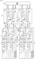
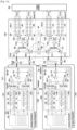
- FIG. 7 is a block diagram of a circuit configuration for providing a feedback path of a transmission signal in an electronic device according to an embodiment, showing a structure of a plurality of antenna modules 701, 702, 703, and 704 and a source RF circuit 707.
- the structure illustrated in FIG. 7 corresponds to the wireless communication module 192 of FIG. 1 .
- FIG. 8 is an illustration of a layout structural of the block diagram of FIG. 7 , schematically showing a structure in which the plurality of antenna modules 701, 702, 703, and 704 and the source RF circuit 707 are arranged in the housing 210.
- feedback coaxial cables implementing a main part of a feedback path are indicated by dotted lines.
- each of the plurality of antenna modules 701, 702, 703, and 704 may include an antenna element and an RF circuit.
- the first antenna module 701 may include a first antenna element 351 and a first RF circuit 711
- the second antenna module 702 may include a second antenna element 352 and a second RF circuit 712.
- each of a third antenna module 703 and a fourth antenna module 704 may include an antenna element.
- the wireless communication circuit for transmitting and receiving an ultra-high frequency radio signal by being electrically connected to the first antenna element 351 and the second antenna element 352 of the first antenna module 701 and the second antenna module 702, respectively, may include a digital modem 708 (e.g., a digital wireless modem).
- the wireless communication circuit may include the source RF circuit 707 that is electrically connected to the digital modem 708 and is configured to generate an IF signal.
- the wireless communication circuit may include the first RF circuit 711, that receives a signal transmitted from the source RF circuit 707, for example, an IF signal, to transmit a transmission signal through the first antenna element 351 and the second RF circuit 712 that receives a transmission signal from the RF circuit 707 to transmit the transmission signal through the second antenna element 352.
- the wireless communication circuit may include RF circuits connected with antenna elements of the third antenna module 703 and the fourth antenna module 704.
- the digital modem 708 may perform modulation/demodulation and channel encoding/decoding with respect to transmission and reception signals, for example, in a digital stage.
- the second antenna element 352 When the first antenna element 351 is arranged at the first position of the housing 210, the second antenna element 352 may be arranged at the second position that is separated from the first position of the housing 210.
- the first RF circuit 711 may be arranged at a third position that is closer to the first position than to the second position.
- the second RF circuit 712 may be arranged at a fourth position that is closer to the second position than to the first position.
- the first antenna element 351 and the first RF circuit 711 are installed adjacent to each other and are coupled through PCB wiring.
- the second antenna element 352 and the second RF circuit 712 may be coupled through PCB wiring.
- the antenna element (e.g., the third antenna element) of the third antenna module 703 may be arranged at a fifth position that is separated from the first position to the fourth position in the housing 210.
- the antenna element (e.g., the fourth antenna element) of the fourth antenna module 704 may be arranged at a sixth position that is separated from the first position to the fifth position in the housing 210.
- the RF circuit (e.g., the third RF circuit) of the third antenna module 703 may be arranged at a seventh position that is close to the fifth position.
- the RF circuit (e.g., the fourth RF circuit) of the fourth antenna module 704 may be arranged at an eighth position that is close to the sixth position.
- the source RF circuit 707 is connected with the first through fourth antenna modules 701, 702, 703, and 704 (respective RF circuits included therein) through a first electrical path 301, a second electrical path 302, a fourth electrical path 303, and a fifth electrical path 304, respectively.
- the first, second, fourth, and fifth electrical paths 301, 302, 303, and 304 may be formed using coaxial cables.
- Respective coaxial cables connecting the source RF circuit 707 with the first through fourth antenna modules 701, 702, 703, and 704 may be designed in their types, lengths, and so forth based on optimal arrangement, signal loss, and phase delay of a signal.
- At least one of the first, second, fourth, and fifth electrical paths 301, 302, 303, and 304 may be implemented using a coaxial cable.
- the first antenna element 351 may be, for example, a radiation element array (4x4 radiation element array) including 16 radiation elements.
- the at least one RF transmission/reception signal processing circuit may include a plurality of, for example, 16 transmission/reception signal processing circuits 326-1, ..., 326-n to process transmission/reception signals for the respective radiation elements of the first antenna element 351.
- the first RF circuit 711 may include a frequency up/down converter for up-converting a transmission signal (e.g., an IF signal) transmitted from the source RF circuit 707 into a radio signal (an RF signal) in an ultra-high frequency band or down-converting a reception signal in the ultra-high frequency band into an IF signal.
- the frequency up/down converter may include a local signal generator 323, a reception mixer 324, a transmission mixer 327, or the like.
- the frequency up/down converter may not be included in the first RF circuit 711.
- the local signal generator 323 of the frequency up/down converter that may be included in the first RF circuit 711 may be configured to generate a local signal therein, but may also be configured to generate a local signal LO_A by using (e.g., frequency multiplication) a reference local signal transmitted from the source RF circuit 707 for signal synchronization as in an example of FIG. 7 .
- the at least one RF transmission/reception signal processing circuits may include 16 transmission/reception signal processing circuits 336-1, ..., 336-n. Between the transmission/reception transition switch 332 and the plurality of transmission/reception signal processing circuits 336-1, ..., 336-n is provided a combiner 335-1 and a divider 335-2 for dividing and combining 16 transmission/reception signals.
- RF circuits included in the third antenna module 703 and the fourth antenna module 704 may include configurations corresponding to the first RF circuit 711 and the second RF circuit 712.
- the transmission ABB 368 may receive I/Q signals converted by a digital-to-analog converter (DAC) from the digital modem 708 and perform filtering, amplification, or the like.
- the transmission ABB 368 may include, for example, a flexible low pass filter (FLPF), a programmable gain-controlled amplifier (PGCA), or the like.
- the first source RF circuit 307-1 may be configured to deliver transmission/reception signals to the first antenna module 701 and the third antenna module 703 for diversity implementation.
- a connection path between the transmission/reception transition switch 363 and the first antenna module 701 and the third antenna module 703 may include a combiner/divider 362 that may be implemented as a 2-way combiner/divider.
- the first through fourth RF circuits 711, 712, ..., of the first through fourth antenna modules 701, 702, 703, and 704 and the source RF circuit 707 may be configured as described above. However, such configurations are merely examples, and various circuit configurations for generating, converting, amplifying or filtering an IF frequency and an RF frequency in a general wireless communication technique may be added or changed.
- the source RF circuit 707 may selectively operate any one of a group of the first antenna module 701 and the third antenna module 703 and a group of the second antenna module 702 and the fourth antennal module 704, based on a current propagation environment, transmission characteristics, and so forth, according to MIMO. For example, any one of the first RF circuit 711 of the first antenna module 701 and the second RF circuit 712 of the second antenna module 702 may operate selectively (e.g., alternately). For example, any one of a third RF circuit of the third antenna module 703 and a fourth RF circuit of the fourth antenna module 704 may operate selectively (e.g., alternately).
- the first RF circuit 711 of the first antenna module 701 may be configured to transmit a feedback signal (e.g., a first feedback signal) associated with a transmission signal thereof to the source RF circuit 707 through an electrical path connecting the second antenna module 702 with the source RF circuit 707, for example, the second electrical path 302, by using the third electrical path 731.
- the second RF circuit 712 of the second antenna module 702 may be configured to transmit a feedback signal (e.g., a second feedback signal) associated with a transmission signal thereof to the source RF circuit 707 through an electrical path connecting the first antenna module 701 with the source RF circuit 707, for example, the first electrical path 301, by using the third electrical path 731.
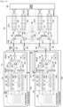
- Internal circuit configurations of the first through fourth antenna modules 701, 702, 703, and 704 and the first through fourth RF circuits 711, 712,... thereof according to the embodiment illustrated in FIGs. 11 and 12 may be the same as or similar with that illustrated in FIG. 7 .
- the antenna module 1301 may include the first antenna element 351 and the first RF circuit 1311.
- the second antenna module 1302 may include the second antenna element 352 and the second RF circuit 1312.
- the first through fourth antenna modules 1301, 1302, 1303, and 1304 (and internal RF circuits thereof) may be connected with the source RF circuit 707 through coaxial cables forming respective electrical paths.
- Basic configurations and operations for processing transmission/reception signals in the respective RF circuits 1311, 1312, ..., and the source RF circuit 707 may be the same as or similar with corresponding configurations and operations shown in FIG. 7 .
- the first RF circuit 1311 may include a first coupler included in a wireless signal transmission path, a first switch 1313 electrically connected to the first coupler and a first end of the third electrical path 1331, or a second switch 1315 included in a wireless signal reception path.
- the second RF circuit 1312 may include a second coupler included in the wireless signal transmission path, a second switch 1323 electrically connected to the first coupler and a second end of the third electrical path 1331, or a fourth switch 1325 included in the wireless signal reception path.
- the second coupler may include a plurality of (e.g., 16) sub couplers 1324-1, ..., 1324-n for coupling a part of a transmission signal for each of a plurality of (e.g., 16) radiation elements included in the second antenna element 352 and branching the same, or a combiner 1320 for combining signals of the plurality of the sub couplers 1324-1, ..., 1324-n.
- a plurality of (e.g., 16) sub couplers 1324-1, ..., 1324-n for coupling a part of a transmission signal for each of a plurality of (e.g., 16) radiation elements included in the second antenna element 352 and branching the same, or a combiner 1320 for combining signals of the plurality of the sub couplers 1324-1, ..., 1324-n.
- a coupling structure of a feedback path according to the embodiment illustrated in FIG. 13 may provide a feedback signal with respect to a radio signal finally transmitted from an immediately previous stage of an antenna element, thereby providing a more accurate feedback signal in relation to a transmission signal depending on circumstances.
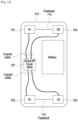
- the first and second RF circuits 1411 and 1412 in the first and second antenna modules 1401 and 1402 may not include frequency-up/down converters for frequency-up/down conversion.
- a first source RF circuit 1407-1 of the source RF circuit 1407 may include an additional local signal generator 1423, a reception mixer 1424, a transmission mixer 1427, and so forth to convert a transmission IF signal back into an RF signal and to convert a reception RF signal into an IF signal.
- a second source RF circuit 1407-2 of the source RF circuit 1407 may also include an additional local signal generator 1433, a reception mixer 1434, a transmission mixer 1437, and so forth.
- related components including the third electrical path 731 for forming a feedback path of a transmission signal between the first antenna module 1401 and the second antenna module 1402 and related components including the sixth electrical path 732 for forming a feedback path of a transmission signal between the third antenna module 1403 and the fourth antenna module 1404 may be the same as or similar with the structure of the embodiment illustrated in FIG. 7 .
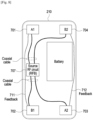
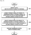
- FIG. 15 is a flowchart of a method of providing a feedback path of a transmission signal in an electronic device according to an embodiment.
- the operations illustrated in FIG. 15 may be performed under control of, for example, a source RF circuit, a digital modem, or other separate external control processes.
- the electronic device identifies an active/inactive state of a plurality of antennas (e.g., a plurality of antenna modules or a plurality of antenna elements) in step (also can be referred to be operation) 1501.
- a plurality of antennas e.g., a plurality of antenna modules or a plurality of antenna elements
- step 1503 the electronic device connects a feedback signal with respect to a transmission signal of an antenna currently in the active state with a path of a reception signal of an antenna currently in the inactive state, based on the identified result.
- step 1505 the electronic device identifies the feedback signal with respect to the transmission signal of the antenna currently in the active state through the connected path of the reception signal of the antenna in the inactive state.
- step 1507 the electronic device performs associated transmission control operations such as output magnitude adjustment or the like with respect to the transmission signal based on the identified feedback signal.
- the electronic device may alternately identify the active/inactive states of the plurality of antennas.
- an IF frequency band and an RF frequency band are described as, for example, an 11 GHz band and a 28 GHz band in various embodiments of the present disclosure, the RF frequency band may also be applied to process a radio signal in various bands such as a 38 GHz band, a 60 GHz band, and so forth in various embodiments.
- each antenna module is described as transmitting and receiving an RF signal in the same frequency band, but various embodiments of the present disclosure may also be applied to a case with different frequency bands. For example, when the first antenna module processes 28 GHz and the second antenna module processes 39 GHz and they process an RF signal obtained by multiplication by a reference local signal having the same frequency, then a feedback path therebetween may also be formed.
- An antenna element to which various embodiments is applied is implemented as a patch-type radiation element array in the foregoing description, but the radiation element array may be a dipole type or a hybrid type in which a patch type and a dipole type are partially implemented.
- an electronic device may also be provided in which a housing is at least partially formed of a metal material and at least a part of the metal material part is implemented with a plurality of antenna elements, and also in this case, at least some of various embodiments may be applied.
- an electronic device includes the housing 210, the first antenna element 351 arranged at a first position inside or on the housing, the second antenna element 352 arranged at a second position, which is separated from the first position, inside or on the housing, and a wireless communication circuit arranged inside the housing and electrically connected to the first antenna element and the second antenna element, in which the wireless communication circuit includes the digital modem 708, the source RF circuit 707 electrically connected to the digital modem 708 and configured to generate an IF signal, the first RF circuit 711 arranged at a third position closer to the first position than to the second position, the second RF circuit 712 arranged at a fourth position closer to the second position than to the first position, the first RF circuit and the second RF circuit being configured to alternately receive a signal transmitted from the source RF circuit to transmit a transmission signal through the first antenna element and the second antenna element, respectively, a first electrical path between the source RF circuit and the first RF circuit, a second electrical path between the source RF circuit and the second
- At least one of the first electrical path, the second electrical path, or the third electrical path 731 may include a coaxial cable.
- the first RF circuit 711 includes a first RF transmission path, a first RF reception path, the first coupler 714 included on the first RF transmission path, the first switch 713 electrically connected to the first coupler and a first end of the third electrical path, and the second switch 715 included on the first RF reception path and electrically connected to the first switch, and the first RF circuit is configured to provide a first feedback signal from the first coupler through the first switch, the third electrical path, and the second electrical path, while transmitting the transmission signal through the first antenna element.
- the second RF circuit 712 includes a second RF transmission path, a second RF reception path, the second coupler 724 included on the second RF transmission path, the third switch 723 electrically connected to the second coupler and a second end of the third electrical path, and the second switch 725 included on the first RF reception path and electrically connected to the first switch, and the first RF circuit is configured to provide a first feedback signal from the first coupler through the first switch, the third electrical path, and the second electrical path, while transmitting the transmission signal through the first antenna element.
- At least one of the first switch 713 or the third switch 723 includes an SPDT switch.
- the IF signal has a frequency between 5 GHz and 6 GHz, and the transmission signal has a frequency between 25 GHz and 30 GHz.
- the electronic device may further include a third antenna element arranged at a fifth position, which is separated from the first through fourth positions, inside or on the housing 210 and a fourth second antenna element arranged at a sixth position, which is separated from the first through fifth positions, inside or on the housing, in which the wireless communication circuit includes a third RF circuit arranged at a seventh position that is closest to the fifth position among the first through sixth positions, a fourth RF circuit arranged at an eighth position that is closest to the sixth position among the first through seventh positions, the third RF circuit and the fourth RF circuit being configured to alternately receive a signal transmitted from the source RF circuit to transmit a transmission signal through the third antenna element and the fourth antenna element, respectively, a fourth electrical path between the source RF circuit and the third RF circuit, a fifth electrical path between the source RF circuit and the fourth RF circuit, and the sixth electrical path 732 between the third RF circuit and the fourth RF circuit, in which the third RF circuit may be configured to transmit a third feedback associated with the transmission signal
- the housing 210 may include a front plate and a rear plate directed in a direction opposite to the front plate, and the housing may have a rectangular shape including a first side having a first length, a second side having a second length longer than the first length, a third side having the first length, and a fourth side having the second length, and the first RF circuit and the second RF circuit may be closer to the first side than to the third side, and the third RF circuit and the fourth RF circuit may be closer to the third side than to the first side.
- the first RF circuit 711 and the third RF circuit may be arranged diagonally when viewed from a top of the front plate of the housing, and are configured to transmit transmission signals at the same time.
- the second RF circuit 212 and the fourth RF circuit may be arranged diagonally when viewed from the top of the front plate of the housing, and may be configured not to transmit the transmission signals when the first RF circuit and the third RF circuit transmit the transmission signals.
- the first antenna element 351 may include a plurality of radiation elements
- the first coupler may include the plurality of sub couplers 1314-1, ..., 1314-n provided for each of the plurality of radiation elements and the combiner 1310 configured to combine signals of the plurality of sub couplers.
- the source RF circuit 707 may be configured to generate an RF signal by using the IF signal.
- a method for providing a feedback path of a transmission signal in an electronic device includes operation 1501 of identifying active/inactive states of a plurality of antennas, operation 1503 of connecting a feedback signal with respect to a transmission signal of an antenna currently in the active state with a path of a reception signal of an antenna currently in the inactive state, and operation 1505 of identifying the feedback signal with respect to the transmission signal of the antenna currently in the active state through the path of the reception signal of the antenna currently in the inactive state.
- the active/inactive states of the plurality of antennas may be set alternately.
- an apparatus for providing a feedback path of a transmission signal in an electronic device includes a first antenna element, a second antenna element, a first RF circuit configured to process a radio signal transmitted and received through the first antenna element, a second RF circuit configured to process a radio signal transmitted and received through the second antenna element, the first feedback electrical path 731 electrically connecting the first RF circuit with the second RF circuit, the first coupler 714 included on the first RF circuit, the first switch 713 electrically connected to the first coupler and a first end of the first feedback electrical path, the second switch 715 included on a reception path of the first RF circuit and electrically connected to the first switch, the second coupler 724 included on a transmission path of the second RF circuit, the third switch 723 electrically connected to the second coupler and a second end of the first feedback electrical path, and the fourth switch 725 included on a reception path of the second RF circuit and electrically connected to the third switch.
- transmission operations of the first RF circuit 711 and the second RF circuit 712 may be performed alternately, and the first RF circuit 711 may be configured to provide a first feedback signal coupled from the first coupler to the second RF circuit 712 through the first switch and the first feedback electrical path, while transmitting the transmission signal through the first antenna element, and the second RF circuit 712 is configured to receive the first feedback signal provided from the first RF circuit on a reception path of the second RF circuit through the third switch and the fourth switch.
- the second RF circuit 712 may be configured to provide a second feedback signal coupled from the second coupler to the first RF circuit through the third switch and the first feedback electrical path, while transmitting the transmission signal through the second antenna element 352, and the first RF circuit 711 may be configured to receive the second feedback signal provided from the second RF circuit on a reception path of the first RF circuit through the first switch and the second switch.
- the first feedback path 731 may include a coaxial cable.
- At least one of the first through fourth switches 713, 715, 723, and 725 may include an SPDT switch.
- the electronic device and the method for providing the feedback path of the transmission signal in the electronic device may reduce some components for processing an ultra-high frequency signal (and a feedback signal), thereby reducing a loss in an internal space of the electronic device and improving the mounting property of the feedback path.
Landscapes
- Engineering & Computer Science (AREA)
- Computer Networks & Wireless Communication (AREA)
- Signal Processing (AREA)
- Physics & Mathematics (AREA)
- Electromagnetism (AREA)
- Telephone Set Structure (AREA)
- Transceivers (AREA)
Claims (9)
- Elektronische Vorrichtung (200), die Folgendes umfasst:ein Gehäuse (210);ein erstes Antennenelement (351), das an einer ersten Position innerhalb des Gehäuses (210) oder an diesem angeordnet ist;ein zweites Antennenelement (352), das an einer zweiten Position, die von der ersten Position getrennt ist, innerhalb des Gehäuses (210) oder an diesem angeordnet ist; undeine drahtlose Kommunikationsschaltung, die innerhalb des Gehäuses (210) angeordnet und elektrisch mit dem ersten Antennenelement (351) und dem zweiten Antennenelement (352) verbunden ist,wobei die drahtlose Kommunikationsschaltung Folgendes umfasst:ein drahtloses Modem (708);eine Quellen-Hochfrequenzschaltung (HF-Schaltung) (707), die elektrisch mit dem drahtlosen Modem (708) verbunden und so ausgelegt ist, dass sie ein Zwischenfrequenzsignal (IF-Signal, Intermediate Frequency) erzeugt;eine erste HF-Schaltung (711), die an einer dritten Position näher an der ersten Position als an der zweiten Position angeordnet ist;eine zweite HF-Schaltung (712), die an einer vierten Position näher an der zweiten Position als an der ersten Position angeordnet ist, wobei die erste HF-Schaltung (711) und die zweite HF-Schaltung (712) so ausgelegt sind, dass sie abwechselnd ein von der Quellen-HF-Schaltung (707) übertragenes Signal empfangen, um ein Übertragungssignal über das erste Antennenelement (351) bzw. das zweite Antennenelement (352) zu übertragen;einen ersten elektrischen Pfad (301) zwischen der Quellen-HF-Schaltung (707) und der ersten HF-Schaltung (711);einen zweiten elektrischen Pfad (302) zwischen der Quellen-HF-Schaltung (707) und der zweiten HF-Schaltung (712); undeinen dritten elektrischen Pfad (731; 1331) zwischen der ersten HF-Schaltung (711) und der zweiten HF-Schaltung (712),wobei die erste HF-Schaltung (711) so ausgelegt ist, dass sie eine erste Rückkopplung, die mit dem von ihr stammenden Übertragungssignal verbunden ist, über den dritten elektrischen Pfad (731; 1331) und den zweiten elektrischen Pfad (302) an die Quellen-HF-Schaltung (707) überträgt, und wobei die zweite HF-Schaltung (712) so ausgelegt ist, dass sie eine zweite Rückkopplung, die mit dem von ihr stammenden Übertragungssignal verbunden ist, über den dritten elektrischen Pfad (731; 1331) und den ersten elektrischen Pfad (301) an die Quellen-HF-Schaltung (707) überträgt;dadurch gekennzeichnet, dass die erste HF-Schaltung (711) Folgendes umfasst:einen ersten HF-Übertragungspfad;einen ersten HF-Empfangspfad;einen ersten Koppler (714), der in dem ersten HF-Übertragungspfad enthalten ist;einen ersten Schalter (713; 1313), der elektrisch mit dem ersten Koppler (714) und einem ersten Ende des dritten elektrischen Pfads (731; 1331) verbunden ist; undeinen zweiten Schalter (715; 1315), der in dem ersten HF-Empfangspfad vorhanden ist und elektrisch mit dem ersten Schalter (713; 1313) verbunden ist, undwobei die erste HF-Schaltung (711) so ausgelegt ist, dass sie ein von dem ersten Koppler (714) stammendes erstes Rückkopplungssignal über den ersten Schalter (713; 1313), den dritten elektrischen Pfad (731; 1331) und den zweiten elektrischen Pfad (302) bereitstellt, während das Übertragungssignal über das erste Antennenelement (351) übertragen wird.
- Elektronische Vorrichtung (200) nach Anspruch 1, wobei die zweite HF-Schaltung (712) Folgendes umfasst:einen zweiten HF-Übertragungspfad;einen zweiten HF-Empfangspfad;einen zweiten Koppler (724), der in dem zweiten HF-Übertragungspfad enthalten ist;einen dritten Schalter (723), der elektrisch mit dem zweiten Koppler (724) und einem zweiten Ende des dritten elektrischen Pfads (731; 1331) verbunden ist; undeinen vierten Schalter (725; 1325), der in dem zweiten HF-Empfangspfad vorhanden ist und elektrisch mit dem dritten Schalter (713) verbunden ist, undwobei die zweite HF-Schaltung (712) so ausgelegt ist, dass sie ein zweites Rückkopplungssignal von dem zweiten Koppler (724) über den dritten Schalter (723), den dritten elektrischen Pfad (731; 1331), den ersten Schalter (713; 1313) und den ersten elektrischen Pfad (301) bereitstellt, während das Übertragungssignal durch das zweite Antennenelement (352) übertragen wird.
- Elektronische Vorrichtung (200) nach Anspruch 1, die ferner Folgendes umfasst:ein drittes Antennenelement (353), das an einer fünften Position, die von der ersten, zweiten, dritten und vierten Position getrennt ist, innerhalb des Gehäuses (210) oder an diesem angeordnet ist; undein viertes Antennenelement (354), das an einer sechsten Position, die von der ersten, zweiten, dritten, vierten und fünften Position getrennt ist, innerhalb des Gehäuses (210) oder an diesem angeordnet ist,wobei die drahtlose Kommunikationsschaltung Folgendes umfasst:eine dritte HF-Schaltung, die an einer siebten Position angeordnet ist, die der fünften Position unter der ersten, zweiten, dritten, vierten, fünften und sechsten Position am nächsten ist;eine vierte HF-Schaltung, die an einer achten Position angeordnet ist, die der sechsten Position unter der ersten bis siebten Position am nächsten ist, wobei die dritte HF-Schaltung und die vierte HF-Schaltung so ausgelegt sind, dass sie abwechselnd ein von der Quellen-HF-Schaltung (707) übertragenes Signal empfangen, um ein Übertragungssignal über das dritte Antennenelement (353) bzw. das vierte Antennenelement (354) zu übertragen;einen vierten elektrischen Pfad (303) zwischen der Quellen-HF-Schaltung (707) und der dritten HF-Schaltung;einen fünften elektrischen Pfad (304) zwischen der Quellen-HF-Schaltung (707) und der vierten HF-Schaltung; undeinen sechsten elektrischen Pfad (732; 1332) zwischen der dritten HF-Schaltung und der vierten HF-Schaltung,wobei die dritte HF-Schaltung so ausgelegt ist, dass sie eine dritte Rückkopplung, die mit dem von ihr stammenden Übertragungssignal verbunden ist, über den sechsten elektrischen Pfad (732; 1332) und den fünften elektrischen Pfad (304) an die Quellen-HF-Schaltung (707) überträgt, undwobei die vierte HF-Schaltung so ausgelegt ist, dass sie eine vierte Rückkopplung, die mit dem von ihr stammenden Übertragungssignal verbunden ist, über den sechsten elektrischen Pfad (732; 1332) und den vierten elektrischen Pfad (303) an den HF-Quellenschaltkreis (707) überträgt.
- Elektronische Vorrichtung (200) nach Anspruch 3, wobei das Gehäuse (210) eine vordere Platte (210A) und eine in eine Richtung entgegengesetzt zu der vorderen Platte (210A) gerichtete hintere Platte (210B) umfasst,wobei das Gehäuse (210) eine rechteckige Form aufweist, die eine erste Seite mit einer ersten Länge, eine zweite Seite mit einer zweiten Länge, die größer als die erste Länge ist, eine dritte Seite mit der ersten Länge und eine vierte Seite mit der zweiten Länge umfasst,wobei die erste HF-Schaltung (711) und die zweite HF-Schaltung (712) näher an der ersten Seite liegen als an der dritten Seite, undwobei die dritte HF-Schaltung und die vierte HF-Schaltung näher an der dritten Seite als an der ersten Seite liegen.
- Elektronische Vorrichtung (200) nach Anspruch 4, wobei die erste HF-Schaltung (711) und die dritte HF-Schaltung von einer Oberseite der vorderen Platte (210A) des Gehäuses (210) aus gesehen diagonal angeordnet sind und so ausgelegt sind, dass sie gleichzeitig Übertragungssignale übertragen.
- Elektronische Vorrichtung (200) nach Anspruch 5, wobei die zweite HF-Schaltung (712) und die vierte HF-Schaltung von der Oberseite der vorderen Platte (210A) des Gehäuses (210) aus gesehen diagonal angeordnet sind und so ausgelegt sind, dass sie die Übertragungssignale nicht übertragen, wenn die erste HF-Schaltung (711) und die dritte HF-Schaltung die Übertragungssignale übertragen.
- Elektronische Vorrichtung (200) nach Anspruch 1, wobei die erste Antenne (351) eine Vielzahl von Strahlungselementen umfasst, und
der erste Koppler (714) Folgendes umfasst:eine Vielzahl von Unterkopplern (1314-1, ..., 1314-n), die für jedes aus der Vielzahl von Strahlungselementen vorgesehen sind; undeinen Kombinierer (1310), der so ausgelegt ist, dass er Signale der Vielzahl von Unterkopplern (1314-1, ..., 1314-n) kombiniert. - Elektronische Vorrichtung (200) nach Anspruch 2, wobei die zweite Antenne (352) eine Vielzahl von Strahlungselementen umfasst, und
der zweite Koppler (724) Folgendes umfasst:eine Vielzahl von Unterkopplern (1324-1, ..., 1324-n), die für jedes aus der Vielzahl von Strahlungselementen der zweiten Antenne (352) vorgesehen sind; undeinen Kombinierer (1320), der so ausgelegt ist, dass er Signale der Vielzahl von Unterkopplern (1314-1, ..., 1314-n) kombiniert. - Elektronische Vorrichtung (200) nach Anspruch 1, wobei die Quellen-HF-Schaltung (707) so ausgelegt ist, dass sie unter Verwendung des IF-Signals ein RF-Signal erzeugt.
Applications Claiming Priority (2)
| Application Number | Priority Date | Filing Date | Title |
|---|---|---|---|
| KR1020170154920A KR102495595B1 (ko) | 2017-11-20 | 2017-11-20 | 전자 장치 및 전자 장치에서의 송신 신호의 피드백 경로 제공 방법 |
| PCT/KR2018/014178 WO2019098783A1 (en) | 2017-11-20 | 2018-11-19 | Electronic device and method for providing feedback path of transmission signal |
Publications (3)
| Publication Number | Publication Date |
|---|---|
| EP3673584A1 EP3673584A1 (de) | 2020-07-01 |
| EP3673584A4 EP3673584A4 (de) | 2020-10-14 |
| EP3673584B1 true EP3673584B1 (de) | 2023-12-27 |
Family
ID=66532641
Family Applications (1)
| Application Number | Title | Priority Date | Filing Date |
|---|---|---|---|
| EP18878586.9A Active EP3673584B1 (de) | 2017-11-20 | 2018-11-19 | Elektronische vorrichtung und verfahren zur bereitstellung eines rückkopplungspfades eines übertragungssignals |
Country Status (4)
| Country | Link |
|---|---|
| US (1) | US10608706B2 (de) |
| EP (1) | EP3673584B1 (de) |
| KR (1) | KR102495595B1 (de) |
| WO (1) | WO2019098783A1 (de) |
Families Citing this family (6)
| Publication number | Priority date | Publication date | Assignee | Title |
|---|---|---|---|---|
| US10615839B2 (en) * | 2018-02-13 | 2020-04-07 | Murata Manufacturing Co., Ltd. | High-frequency-signal transceiver circuit |
| KR102758032B1 (ko) * | 2019-08-02 | 2025-01-21 | 삼성전자주식회사 | Fpcb를 포함하는 전자 장치 |
| WO2021025471A1 (en) * | 2019-08-05 | 2021-02-11 | Samsung Electronics Co., Ltd. | Antenna module and electronic device for using the antenna module |
| US11005519B1 (en) * | 2020-05-01 | 2021-05-11 | UTVATE Corporation | Isolation methods for full-duplex antenna systems |
| EP4354742A1 (de) * | 2022-10-12 | 2024-04-17 | Nokia Technologies Oy | Flexibler empfang |
| WO2024085663A1 (ko) * | 2022-10-19 | 2024-04-25 | 삼성전자 주식회사 | 보안 연결을 제공하는 전자 장치 및 그 동작 방법 |
Family Cites Families (16)
| Publication number | Priority date | Publication date | Assignee | Title |
|---|---|---|---|---|
| EP1791278A1 (de) * | 2005-11-29 | 2007-05-30 | Interuniversitair Microelektronica Centrum (IMEC) | Verfahren und Vorrichtung zum Eichen von MIMO-Systemen |
| US8045926B2 (en) * | 2008-10-15 | 2011-10-25 | Nokia Siemens Networks Oy | Multi-transceiver architecture for advanced Tx antenna monitoring and calibration in MIMO and smart antenna communication systems |
| US20100309901A1 (en) * | 2009-06-03 | 2010-12-09 | Harris Corporation | Systems and methods for maintaining a controlled power output at an antenna port over a range of frequencies defined by two or more frequency bands |
| US8295212B2 (en) * | 2009-08-05 | 2012-10-23 | Alcatel Lucent | System and method for TDD/TMA with hybrid bypass switch of receiving amplifier |
| GB2476252B (en) * | 2009-12-17 | 2012-10-24 | Socowave Technologies Ltd | Communication unit, integrated circuit and method of diverse polarisation |
| WO2011119659A1 (en) * | 2010-03-23 | 2011-09-29 | Rf Micro Devices, Inc. | Adaptive antenna neutralization network |
| JP6156907B2 (ja) * | 2013-01-15 | 2017-07-05 | 国立研究開発法人情報通信研究機構 | 無線装置 |
| US20140242914A1 (en) * | 2013-02-22 | 2014-08-28 | Samsung Electronics Co., Ltd. | Method and apparatus for calibrating multiple antenna arrays |
| KR102323130B1 (ko) * | 2013-11-27 | 2021-11-10 | 삼성전자 주식회사 | 하이브리드 빔포밍 기반 오픈-루프 mimo 전송 방법 및 장치 |
| WO2015166305A1 (en) * | 2014-04-30 | 2015-11-05 | Telefonaktiebolaget L M Ericsson (Publ) | Multi-sector antenna integrated radio unit |
| KR102302259B1 (ko) | 2015-03-31 | 2021-09-15 | 삼성전자주식회사 | 다중 안테나를 사용하는 시스템에서 채널을 추정하여 rf 빔을 선택하는 방법 및 장치 |
| US20160308276A1 (en) * | 2015-04-14 | 2016-10-20 | Dell Products L.P. | System and method for dynamic switching of antennas |
| KR102459683B1 (ko) * | 2015-07-09 | 2022-10-28 | 삼성전자주식회사 | 무선 주파수 모듈에서의 교정장치 및 방법 |
| US10103431B2 (en) * | 2016-04-21 | 2018-10-16 | Google Llc | Phased array antenna calibration |
| US10670699B2 (en) * | 2017-09-07 | 2020-06-02 | Nxp B.V. | RF radar device BIST using noise injection |
| US10910714B2 (en) * | 2017-09-11 | 2021-02-02 | Qualcomm Incorporated | Configurable power combiner and splitter |
-
2017
- 2017-11-20 KR KR1020170154920A patent/KR102495595B1/ko active Active
-
2018
- 2018-11-19 WO PCT/KR2018/014178 patent/WO2019098783A1/en not_active Ceased
- 2018-11-19 EP EP18878586.9A patent/EP3673584B1/de active Active
- 2018-11-20 US US16/196,490 patent/US10608706B2/en not_active Expired - Fee Related
Also Published As
| Publication number | Publication date |
|---|---|
| KR20190057678A (ko) | 2019-05-29 |
| US10608706B2 (en) | 2020-03-31 |
| US20190158154A1 (en) | 2019-05-23 |
| EP3673584A4 (de) | 2020-10-14 |
| KR102495595B1 (ko) | 2023-02-06 |
| EP3673584A1 (de) | 2020-07-01 |
| WO2019098783A1 (en) | 2019-05-23 |
Similar Documents
| Publication | Publication Date | Title |
|---|---|---|
| EP3673584B1 (de) | Elektronische vorrichtung und verfahren zur bereitstellung eines rückkopplungspfades eines übertragungssignals | |
| US11342981B2 (en) | Electronic device including antenna module | |
| EP3584943B1 (de) | Elektronische vorrichtung mit einer mehrzahl von schaltern, die selektiv eine antenne mit einer mehrzahl von speiseanschlüssen mit einer kommunikationsschaltung verbinden, und ansteuerungsverfahren dafür | |
| US11831072B2 (en) | Antenna module using metal bezel and electronic device including thereof | |
| US11800667B2 (en) | Antenna and electronic device including same | |
| EP4044440B1 (de) | Elektronische vorrichtung und antennenumschaltverfahren dafür | |
| US11101827B2 (en) | Electronic device comprising antenna and method for transmitting or receiving signal | |
| US12047137B2 (en) | Electronic device for detecting external object using antenna array and operation method thereof | |
| US10666335B2 (en) | Method of selecting beam and electronic device thereof | |
| KR20200045661A (ko) | 플렉서블 인쇄 회로 기판의 그라운드 층 및 인쇄 회로 기판의 그라운드 층을 전기적으로 연결하는 도전성 구조체를 포함하는 전자 장치 | |
| US11323146B2 (en) | Device and method for calibrating communication module | |
| US20210036434A1 (en) | Electronic device having fpcb | |
| EP3764472B1 (de) | Verfahren zur verarbeitung von signalen unter verwendung von hochfrequenzketten und elektronische vorrichtung dafür | |
| US12542575B2 (en) | Electronic device for processing radio signal and operating method thereof | |
| US11456714B2 (en) | Electronic device for processing radio signal and operating method thereof | |
| US11284478B2 (en) | Electronic device for transmitting data according to communication scheme selected on basis of signal strength from multiple communication schemes and method for operating same | |
| EP4206718A1 (de) | Positionierungsverfahren mit mehreren vorrichtungen und elektronische vorrichtung dafür | |
| US12542997B2 (en) | Method and device for processing audio data obtained via microphone and audio data received via external device into single audio stream | |
| KR20220064874A (ko) | 무선 신호를 처리하기 위한 전자 장치 및 그의 동작 방법 | |
| EP4568121A1 (de) | Elektronische vorrichtung mit mehreren antennen | |
| KR20210029046A (ko) | 전자 장치에서의 빔 측정 방법 및 전자 장치 | |
| US20240223225A1 (en) | Electronic device for processing radio signal for plurality of communication systems and operating method thereof | |
| EP4351020A1 (de) | Elektronische vorrichtung mit einem an eine antenne in einer drahtlosen umgebung angeschlossenen koppler | |
| US11909435B2 (en) | Method for multi-band communication and electronic device thereof | |
| KR20240018328A (ko) | 무선 환경 내에서 안테나와 연결된 커플러를 포함하는 전자 장치 |
Legal Events
| Date | Code | Title | Description |
|---|---|---|---|
| STAA | Information on the status of an ep patent application or granted ep patent |
Free format text: STATUS: THE INTERNATIONAL PUBLICATION HAS BEEN MADE |
|
| PUAI | Public reference made under article 153(3) epc to a published international application that has entered the european phase |
Free format text: ORIGINAL CODE: 0009012 |
|
| STAA | Information on the status of an ep patent application or granted ep patent |
Free format text: STATUS: REQUEST FOR EXAMINATION WAS MADE |
|
| 17P | Request for examination filed |
Effective date: 20200327 |
|
| AK | Designated contracting states |
Kind code of ref document: A1 Designated state(s): AL AT BE BG CH CY CZ DE DK EE ES FI FR GB GR HR HU IE IS IT LI LT LU LV MC MK MT NL NO PL PT RO RS SE SI SK SM TR |
|
| AX | Request for extension of the european patent |
Extension state: BA ME |
|
| A4 | Supplementary search report drawn up and despatched |
Effective date: 20200910 |
|
| RIC1 | Information provided on ipc code assigned before grant |
Ipc: H04B 1/40 20150101AFI20200904BHEP Ipc: H04B 7/0413 20170101ALN20200904BHEP Ipc: H04B 17/14 20150101ALI20200904BHEP |
|
| DAV | Request for validation of the european patent (deleted) | ||
| DAX | Request for extension of the european patent (deleted) | ||
| STAA | Information on the status of an ep patent application or granted ep patent |
Free format text: STATUS: EXAMINATION IS IN PROGRESS |
|
| 17Q | First examination report despatched |
Effective date: 20211123 |
|
| REG | Reference to a national code |
Ref country code: DE Free format text: PREVIOUS MAIN CLASS: H04B0007040400 Ipc: H04B0001400000 Ref country code: DE Ref legal event code: R079 Ref document number: 602018063402 Country of ref document: DE Free format text: PREVIOUS MAIN CLASS: H04B0007040400 Ipc: H04B0001400000 |
|
| RIC1 | Information provided on ipc code assigned before grant |
Ipc: H04B 7/0413 20170101ALN20230628BHEP Ipc: H04B 17/14 20150101ALI20230628BHEP Ipc: H04B 1/40 20150101AFI20230628BHEP |
|
| GRAP | Despatch of communication of intention to grant a patent |
Free format text: ORIGINAL CODE: EPIDOSNIGR1 |
|
| STAA | Information on the status of an ep patent application or granted ep patent |
Free format text: STATUS: GRANT OF PATENT IS INTENDED |
|
| INTG | Intention to grant announced |
Effective date: 20230811 |
|
| GRAS | Grant fee paid |
Free format text: ORIGINAL CODE: EPIDOSNIGR3 |
|
| GRAA | (expected) grant |
Free format text: ORIGINAL CODE: 0009210 |
|
| STAA | Information on the status of an ep patent application or granted ep patent |
Free format text: STATUS: THE PATENT HAS BEEN GRANTED |
|
| AK | Designated contracting states |
Kind code of ref document: B1 Designated state(s): AL AT BE BG CH CY CZ DE DK EE ES FI FR GB GR HR HU IE IS IT LI LT LU LV MC MK MT NL NO PL PT RO RS SE SI SK SM TR |
|
| REG | Reference to a national code |
Ref country code: GB Ref legal event code: FG4D |
|
| REG | Reference to a national code |
Ref country code: CH Ref legal event code: EP |
|
| REG | Reference to a national code |
Ref country code: DE Ref legal event code: R096 Ref document number: 602018063402 Country of ref document: DE |
|
| REG | Reference to a national code |
Ref country code: IE Ref legal event code: FG4D |
|
| PG25 | Lapsed in a contracting state [announced via postgrant information from national office to epo] |
Ref country code: GR Free format text: LAPSE BECAUSE OF FAILURE TO SUBMIT A TRANSLATION OF THE DESCRIPTION OR TO PAY THE FEE WITHIN THE PRESCRIBED TIME-LIMIT Effective date: 20240328 |
|
| REG | Reference to a national code |
Ref country code: LT Ref legal event code: MG9D |
|
| PG25 | Lapsed in a contracting state [announced via postgrant information from national office to epo] |
Ref country code: LT Free format text: LAPSE BECAUSE OF FAILURE TO SUBMIT A TRANSLATION OF THE DESCRIPTION OR TO PAY THE FEE WITHIN THE PRESCRIBED TIME-LIMIT Effective date: 20231227 |
|
| PG25 | Lapsed in a contracting state [announced via postgrant information from national office to epo] |
Ref country code: ES Free format text: LAPSE BECAUSE OF FAILURE TO SUBMIT A TRANSLATION OF THE DESCRIPTION OR TO PAY THE FEE WITHIN THE PRESCRIBED TIME-LIMIT Effective date: 20231227 |
|
| PG25 | Lapsed in a contracting state [announced via postgrant information from national office to epo] |
Ref country code: LT Free format text: LAPSE BECAUSE OF FAILURE TO SUBMIT A TRANSLATION OF THE DESCRIPTION OR TO PAY THE FEE WITHIN THE PRESCRIBED TIME-LIMIT Effective date: 20231227 Ref country code: GR Free format text: LAPSE BECAUSE OF FAILURE TO SUBMIT A TRANSLATION OF THE DESCRIPTION OR TO PAY THE FEE WITHIN THE PRESCRIBED TIME-LIMIT Effective date: 20240328 Ref country code: FI Free format text: LAPSE BECAUSE OF FAILURE TO SUBMIT A TRANSLATION OF THE DESCRIPTION OR TO PAY THE FEE WITHIN THE PRESCRIBED TIME-LIMIT Effective date: 20231227 Ref country code: ES Free format text: LAPSE BECAUSE OF FAILURE TO SUBMIT A TRANSLATION OF THE DESCRIPTION OR TO PAY THE FEE WITHIN THE PRESCRIBED TIME-LIMIT Effective date: 20231227 Ref country code: BG Free format text: LAPSE BECAUSE OF FAILURE TO SUBMIT A TRANSLATION OF THE DESCRIPTION OR TO PAY THE FEE WITHIN THE PRESCRIBED TIME-LIMIT Effective date: 20240327 |
|
| REG | Reference to a national code |
Ref country code: NL Ref legal event code: MP Effective date: 20231227 |
|
| REG | Reference to a national code |
Ref country code: AT Ref legal event code: MK05 Ref document number: 1645498 Country of ref document: AT Kind code of ref document: T Effective date: 20231227 |
|
| PG25 | Lapsed in a contracting state [announced via postgrant information from national office to epo] |
Ref country code: NL Free format text: LAPSE BECAUSE OF FAILURE TO SUBMIT A TRANSLATION OF THE DESCRIPTION OR TO PAY THE FEE WITHIN THE PRESCRIBED TIME-LIMIT Effective date: 20231227 |
|
| PG25 | Lapsed in a contracting state [announced via postgrant information from national office to epo] |
Ref country code: SE Free format text: LAPSE BECAUSE OF FAILURE TO SUBMIT A TRANSLATION OF THE DESCRIPTION OR TO PAY THE FEE WITHIN THE PRESCRIBED TIME-LIMIT Effective date: 20231227 Ref country code: RS Free format text: LAPSE BECAUSE OF FAILURE TO SUBMIT A TRANSLATION OF THE DESCRIPTION OR TO PAY THE FEE WITHIN THE PRESCRIBED TIME-LIMIT Effective date: 20231227 Ref country code: NO Free format text: LAPSE BECAUSE OF FAILURE TO SUBMIT A TRANSLATION OF THE DESCRIPTION OR TO PAY THE FEE WITHIN THE PRESCRIBED TIME-LIMIT Effective date: 20240327 Ref country code: NL Free format text: LAPSE BECAUSE OF FAILURE TO SUBMIT A TRANSLATION OF THE DESCRIPTION OR TO PAY THE FEE WITHIN THE PRESCRIBED TIME-LIMIT Effective date: 20231227 Ref country code: LV Free format text: LAPSE BECAUSE OF FAILURE TO SUBMIT A TRANSLATION OF THE DESCRIPTION OR TO PAY THE FEE WITHIN THE PRESCRIBED TIME-LIMIT Effective date: 20231227 Ref country code: HR Free format text: LAPSE BECAUSE OF FAILURE TO SUBMIT A TRANSLATION OF THE DESCRIPTION OR TO PAY THE FEE WITHIN THE PRESCRIBED TIME-LIMIT Effective date: 20231227 |
|
| PG25 | Lapsed in a contracting state [announced via postgrant information from national office to epo] |
Ref country code: IS Free format text: LAPSE BECAUSE OF FAILURE TO SUBMIT A TRANSLATION OF THE DESCRIPTION OR TO PAY THE FEE WITHIN THE PRESCRIBED TIME-LIMIT Effective date: 20240427 |
|
| PG25 | Lapsed in a contracting state [announced via postgrant information from national office to epo] |
Ref country code: AT Free format text: LAPSE BECAUSE OF FAILURE TO SUBMIT A TRANSLATION OF THE DESCRIPTION OR TO PAY THE FEE WITHIN THE PRESCRIBED TIME-LIMIT Effective date: 20231227 Ref country code: CZ Free format text: LAPSE BECAUSE OF FAILURE TO SUBMIT A TRANSLATION OF THE DESCRIPTION OR TO PAY THE FEE WITHIN THE PRESCRIBED TIME-LIMIT Effective date: 20231227 |
|
| PG25 | Lapsed in a contracting state [announced via postgrant information from national office to epo] |
Ref country code: SK Free format text: LAPSE BECAUSE OF FAILURE TO SUBMIT A TRANSLATION OF THE DESCRIPTION OR TO PAY THE FEE WITHIN THE PRESCRIBED TIME-LIMIT Effective date: 20231227 |
|
| PG25 | Lapsed in a contracting state [announced via postgrant information from national office to epo] |
Ref country code: SM Free format text: LAPSE BECAUSE OF FAILURE TO SUBMIT A TRANSLATION OF THE DESCRIPTION OR TO PAY THE FEE WITHIN THE PRESCRIBED TIME-LIMIT Effective date: 20231227 Ref country code: SK Free format text: LAPSE BECAUSE OF FAILURE TO SUBMIT A TRANSLATION OF THE DESCRIPTION OR TO PAY THE FEE WITHIN THE PRESCRIBED TIME-LIMIT Effective date: 20231227 Ref country code: RO Free format text: LAPSE BECAUSE OF FAILURE TO SUBMIT A TRANSLATION OF THE DESCRIPTION OR TO PAY THE FEE WITHIN THE PRESCRIBED TIME-LIMIT Effective date: 20231227 Ref country code: IT Free format text: LAPSE BECAUSE OF FAILURE TO SUBMIT A TRANSLATION OF THE DESCRIPTION OR TO PAY THE FEE WITHIN THE PRESCRIBED TIME-LIMIT Effective date: 20231227 Ref country code: IS Free format text: LAPSE BECAUSE OF FAILURE TO SUBMIT A TRANSLATION OF THE DESCRIPTION OR TO PAY THE FEE WITHIN THE PRESCRIBED TIME-LIMIT Effective date: 20240427 Ref country code: EE Free format text: LAPSE BECAUSE OF FAILURE TO SUBMIT A TRANSLATION OF THE DESCRIPTION OR TO PAY THE FEE WITHIN THE PRESCRIBED TIME-LIMIT Effective date: 20231227 Ref country code: CZ Free format text: LAPSE BECAUSE OF FAILURE TO SUBMIT A TRANSLATION OF THE DESCRIPTION OR TO PAY THE FEE WITHIN THE PRESCRIBED TIME-LIMIT Effective date: 20231227 Ref country code: AT Free format text: LAPSE BECAUSE OF FAILURE TO SUBMIT A TRANSLATION OF THE DESCRIPTION OR TO PAY THE FEE WITHIN THE PRESCRIBED TIME-LIMIT Effective date: 20231227 |
|
| PG25 | Lapsed in a contracting state [announced via postgrant information from national office to epo] |
Ref country code: PL Free format text: LAPSE BECAUSE OF FAILURE TO SUBMIT A TRANSLATION OF THE DESCRIPTION OR TO PAY THE FEE WITHIN THE PRESCRIBED TIME-LIMIT Effective date: 20231227 Ref country code: PT Free format text: LAPSE BECAUSE OF FAILURE TO SUBMIT A TRANSLATION OF THE DESCRIPTION OR TO PAY THE FEE WITHIN THE PRESCRIBED TIME-LIMIT Effective date: 20240429 |
|
| PG25 | Lapsed in a contracting state [announced via postgrant information from national office to epo] |
Ref country code: PT Free format text: LAPSE BECAUSE OF FAILURE TO SUBMIT A TRANSLATION OF THE DESCRIPTION OR TO PAY THE FEE WITHIN THE PRESCRIBED TIME-LIMIT Effective date: 20240429 Ref country code: PL Free format text: LAPSE BECAUSE OF FAILURE TO SUBMIT A TRANSLATION OF THE DESCRIPTION OR TO PAY THE FEE WITHIN THE PRESCRIBED TIME-LIMIT Effective date: 20231227 |
|
| REG | Reference to a national code |
Ref country code: DE Ref legal event code: R097 Ref document number: 602018063402 Country of ref document: DE |
|
| PG25 | Lapsed in a contracting state [announced via postgrant information from national office to epo] |
Ref country code: DK Free format text: LAPSE BECAUSE OF FAILURE TO SUBMIT A TRANSLATION OF THE DESCRIPTION OR TO PAY THE FEE WITHIN THE PRESCRIBED TIME-LIMIT Effective date: 20231227 |
|
| PG25 | Lapsed in a contracting state [announced via postgrant information from national office to epo] |
Ref country code: DK Free format text: LAPSE BECAUSE OF FAILURE TO SUBMIT A TRANSLATION OF THE DESCRIPTION OR TO PAY THE FEE WITHIN THE PRESCRIBED TIME-LIMIT Effective date: 20231227 |
|
| PLBE | No opposition filed within time limit |
Free format text: ORIGINAL CODE: 0009261 |
|
| STAA | Information on the status of an ep patent application or granted ep patent |
Free format text: STATUS: NO OPPOSITION FILED WITHIN TIME LIMIT |
|
| 26N | No opposition filed |
Effective date: 20240930 |
|
| PG25 | Lapsed in a contracting state [announced via postgrant information from national office to epo] |
Ref country code: SI Free format text: LAPSE BECAUSE OF FAILURE TO SUBMIT A TRANSLATION OF THE DESCRIPTION OR TO PAY THE FEE WITHIN THE PRESCRIBED TIME-LIMIT Effective date: 20231227 |
|
| REG | Reference to a national code |
Ref country code: CH Ref legal event code: PL |
|
| PG25 | Lapsed in a contracting state [announced via postgrant information from national office to epo] |
Ref country code: MC Free format text: LAPSE BECAUSE OF FAILURE TO SUBMIT A TRANSLATION OF THE DESCRIPTION OR TO PAY THE FEE WITHIN THE PRESCRIBED TIME-LIMIT Effective date: 20231227 |
|
| PG25 | Lapsed in a contracting state [announced via postgrant information from national office to epo] |
Ref country code: LU Free format text: LAPSE BECAUSE OF NON-PAYMENT OF DUE FEES Effective date: 20241119 |
|
| REG | Reference to a national code |
Ref country code: CH Ref legal event code: PL |
|
| PG25 | Lapsed in a contracting state [announced via postgrant information from national office to epo] |
Ref country code: CH Free format text: LAPSE BECAUSE OF NON-PAYMENT OF DUE FEES Effective date: 20241130 |
|
| REG | Reference to a national code |
Ref country code: BE Ref legal event code: MM Effective date: 20241130 |
|
| PG25 | Lapsed in a contracting state [announced via postgrant information from national office to epo] |
Ref country code: BE Free format text: LAPSE BECAUSE OF NON-PAYMENT OF DUE FEES Effective date: 20241130 |
|
| PG25 | Lapsed in a contracting state [announced via postgrant information from national office to epo] |
Ref country code: FR Free format text: LAPSE BECAUSE OF NON-PAYMENT OF DUE FEES Effective date: 20241130 |
|
| PG25 | Lapsed in a contracting state [announced via postgrant information from national office to epo] |
Ref country code: IE Free format text: LAPSE BECAUSE OF NON-PAYMENT OF DUE FEES Effective date: 20241119 |
|
| PGFP | Annual fee paid to national office [announced via postgrant information from national office to epo] |
Ref country code: DE Payment date: 20251002 Year of fee payment: 8 |
|
| PGFP | Annual fee paid to national office [announced via postgrant information from national office to epo] |
Ref country code: GB Payment date: 20251001 Year of fee payment: 8 |
|
| PG25 | Lapsed in a contracting state [announced via postgrant information from national office to epo] |
Ref country code: HU Free format text: LAPSE BECAUSE OF FAILURE TO SUBMIT A TRANSLATION OF THE DESCRIPTION OR TO PAY THE FEE WITHIN THE PRESCRIBED TIME-LIMIT; INVALID AB INITIO Effective date: 20181119 |
|
| PG25 | Lapsed in a contracting state [announced via postgrant information from national office to epo] |
Ref country code: CY Free format text: LAPSE BECAUSE OF FAILURE TO SUBMIT A TRANSLATION OF THE DESCRIPTION OR TO PAY THE FEE WITHIN THE PRESCRIBED TIME-LIMIT; INVALID AB INITIO Effective date: 20181119 |