EP3673325B1 - Integriertes faraday-drehgelenk - Google Patents
Integriertes faraday-drehgelenk Download PDFInfo
- Publication number
- EP3673325B1 EP3673325B1 EP18848653.4A EP18848653A EP3673325B1 EP 3673325 B1 EP3673325 B1 EP 3673325B1 EP 18848653 A EP18848653 A EP 18848653A EP 3673325 B1 EP3673325 B1 EP 3673325B1
- Authority
- EP
- European Patent Office
- Prior art keywords
- waveguide
- waveguide component
- optical waveguide
- component
- sections
- Prior art date
- Legal status (The legal status is an assumption and is not a legal conclusion. Google has not performed a legal analysis and makes no representation as to the accuracy of the status listed.)
- Active
Links
Images


Classifications
-
- G—PHYSICS
- G02—OPTICS
- G02F—OPTICAL DEVICES OR ARRANGEMENTS FOR THE CONTROL OF LIGHT BY MODIFICATION OF THE OPTICAL PROPERTIES OF THE MEDIA OF THE ELEMENTS INVOLVED THEREIN; NON-LINEAR OPTICS; FREQUENCY-CHANGING OF LIGHT; OPTICAL LOGIC ELEMENTS; OPTICAL ANALOGUE/DIGITAL CONVERTERS
- G02F1/00—Devices or arrangements for the control of the intensity, colour, phase, polarisation or direction of light arriving from an independent light source, e.g. switching, gating or modulating; Non-linear optics
- G02F1/01—Devices or arrangements for the control of the intensity, colour, phase, polarisation or direction of light arriving from an independent light source, e.g. switching, gating or modulating; Non-linear optics for the control of the intensity, phase, polarisation or colour
- G02F1/09—Devices or arrangements for the control of the intensity, colour, phase, polarisation or direction of light arriving from an independent light source, e.g. switching, gating or modulating; Non-linear optics for the control of the intensity, phase, polarisation or colour based on magneto-optical elements, e.g. exhibiting Faraday effect
- G02F1/095—Devices or arrangements for the control of the intensity, colour, phase, polarisation or direction of light arriving from an independent light source, e.g. switching, gating or modulating; Non-linear optics for the control of the intensity, phase, polarisation or colour based on magneto-optical elements, e.g. exhibiting Faraday effect in an optical waveguide structure
- G02F1/0955—Devices or arrangements for the control of the intensity, colour, phase, polarisation or direction of light arriving from an independent light source, e.g. switching, gating or modulating; Non-linear optics for the control of the intensity, phase, polarisation or colour based on magneto-optical elements, e.g. exhibiting Faraday effect in an optical waveguide structure used as non-reciprocal devices, e.g. optical isolators, circulators
-
- G—PHYSICS
- G02—OPTICS
- G02B—OPTICAL ELEMENTS, SYSTEMS OR APPARATUS
- G02B6/00—Light guides; Structural details of arrangements comprising light guides and other optical elements, e.g. couplings
- G02B6/10—Light guides; Structural details of arrangements comprising light guides and other optical elements, e.g. couplings of the optical waveguide type
- G02B6/12—Light guides; Structural details of arrangements comprising light guides and other optical elements, e.g. couplings of the optical waveguide type of the integrated circuit kind
- G02B6/126—Light guides; Structural details of arrangements comprising light guides and other optical elements, e.g. couplings of the optical waveguide type of the integrated circuit kind using polarisation effects
-
- G—PHYSICS
- G02—OPTICS
- G02F—OPTICAL DEVICES OR ARRANGEMENTS FOR THE CONTROL OF LIGHT BY MODIFICATION OF THE OPTICAL PROPERTIES OF THE MEDIA OF THE ELEMENTS INVOLVED THEREIN; NON-LINEAR OPTICS; FREQUENCY-CHANGING OF LIGHT; OPTICAL LOGIC ELEMENTS; OPTICAL ANALOGUE/DIGITAL CONVERTERS
- G02F1/00—Devices or arrangements for the control of the intensity, colour, phase, polarisation or direction of light arriving from an independent light source, e.g. switching, gating or modulating; Non-linear optics
- G02F1/01—Devices or arrangements for the control of the intensity, colour, phase, polarisation or direction of light arriving from an independent light source, e.g. switching, gating or modulating; Non-linear optics for the control of the intensity, phase, polarisation or colour
- G02F1/0136—Devices or arrangements for the control of the intensity, colour, phase, polarisation or direction of light arriving from an independent light source, e.g. switching, gating or modulating; Non-linear optics for the control of the intensity, phase, polarisation or colour for the control of polarisation, e.g. state of polarisation [SOP] control, polarisation scrambling, TE-TM mode conversion or separation
Definitions
- the non-linear devices the generally low non-linear effect and the need for a high power pump source pose a major problem to on-chip integration.
- the isolators relying on electro-optical effects require a cumbersome space and time dependent modulation scheme and have so far only been shown to work with insufficient suppression ratios.
- Materials with strong magneto-optical activity prove to be very difficult to introduce into integrated photonic circuits. Either these materials show a very low effect or too high optical losses or they pose other problems like the crystal lattice mismatch between silicon and the magneto-optical material.
- the Faraday rotation of silicon is 15°/cm/T at 1.55 ⁇ m which is roughly two orders of magnitude lower than what can be achieved with iron garnets. Assuming a biasing field of 0.5 T, a 6 cm long waveguide is needed to achieve the 45° Faraday rotation necessary for an optical isolator.
- ZHANG CUI ET AL "Monolithically-Integrated TE-mode 1 D Silicon-onInsulator Isolators using Seedlayer-Free Garnet", SCIENTIFIC REPORTS, vol. 7, no. 1, 19 July 2017 (2017-07-19 ), presents an optical waveguide component for providing Faraday rotation to a plane of polarization of linearly polarized light propagating in said waveguide component (TE mode isolator), wherein said waveguide component is made of silicon and having linear waveguide section and a magnetic field generator generating a magnetic field ( Figure 1 ) parallel to the linear waveguide section.
- Morichetti Francesco ET AL "Modelling of Polarization Rotation in Bent Waveguides", 8th International Conference on Transparent Optical Networks - ICTON 2006. Nottingham, United Kingdom, June 18-22, 2006, pages 261-261 , aims to show that the process of polarization conversion in the bend strictly depends on the characteristics of the straight waveguide. Matteo Cherchi ET AL: "Dramatic size reduction of waveguide bends on a micron-scale silicon photonic platform", Optics Express, vol. 21, no.
- US 2003/206681 A1 presents an integrating elements for optical fiber communication systems based on photonic multi-bandgap quasi-crystals having optimized transfer functions.
- US 2007/147725 A1 presents a coupled-waveguide electro-optic switch based on polarisation conversion.
- US 2005/275944 A1 presents optical films and methods of making the same.
- US 2016/011438 A1 presents an on-chip optical polarization controller.
- a polarization dependent isolator, or Faraday isolator 10 as shown in Fig. 1 is made of three main parts, an input polarizer 11 (here polarized vertically), a Faraday rotator 12 and an output polarizer 13, also called analyzer, here polarized at 45°.
- Light traveling in the forward direction becomes polarized vertically by the input polarizer.
- the Faraday rotator will rotate the polarization by 45°.
- the analyzer then enables the light to be transmitted through the isolator.
- Light traveling in the backward direction becomes polarized at 45° by the analyzer.
- the Faraday rotator will again rotate the polarization by 45°. This means the light is polarized horizontally (the rotation is sensitive to direction of propagation). Since the polarizer is vertically aligned, the light will be extinguished.
- a magnetic field B applied to the Faraday rotator in Fig. 1 causes a rotation in the polarization of the light due to the Faraday effect.
- the angle of rotation is ⁇ and d is the length of the rotator.
- the values are chosen to give a rotation of 45°.
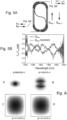
- Fig. 2 is shown the evolution of the polarization for a folded Faraday rotator.
- part A of Fig. 2 is shown a standard Faraday rotator as used for an optical isolator.
- the left part 21 depicts a wave travelling in forward direction; the right part 22 shows a wave traveling in backward direction.
- the polarization will be rotated clockwise to 45° in this example.
- the wave vector k and bias field are opposite.
- the initial polarization of the wave vector in guide 22 is 135°
- the polarization rotation with respect to the wave vector k is counter-clockwise.
- part B two Faraday rotators 23, 24 are connected by a bend 25 that preserves the polarization state.
- the net Faraday rotation is in this case zero.
- part C a similar Faraday rotator assembly is shown as in B, but now the rotators 26, 27 are connected with a birefringent bend 28, that accumulates a 180° phase-shift between the vertical and horizontal polarization.
- the polarization rotation in the two parts adds up to 90° or 270°, depending on the direction of the 180° phase- shift.
- Birefringence is the property of optically non-isotropic transparent materials that the refractive index depends on the polarization direction, i.e. the direction of the electric field. For example, it is observed for crystalline quartz, calcite, sapphire and ruby and in nonlinear crystal materials like LiNbO 3 , LBO and KTP. Often birefringence results from non-cubic crystal structures. In other cases, originally isotropic materials (e.g. crystals with cubic structure and glasses) can become anisotropic due to the application of mechanical stress, or sometimes by application of a strong electric field; both can break their original symmetry.
- birefringence may result from an elliptical shape of the fiber core, from asymmetries of the fiber design or from mechanical stress, e.g. caused by bending.
- form-birefringence can be easily achieved by designing suitable waveguide shapes (e.g. a rectangular strip waveguide), so to ensure different effective index for the two orthogonally polarized (quasi TE and quasi TM) eigenmodes.
- strain and bends can play an important role in mode birefringence, but a key advantage of integrated waveguides is that, once all parameters are known, changing the waveguide shape enable a total control of the birefringence, also in presence of strain and bends.
- the magneto-optical activity of silicon can be exploited through either of two effects: the magneto-optical phase shift or Faraday rotation.
- silicon is usually the material with the highest refractive index used in integrated photonic systems and therefore serves as waveguide core material.
- the high index contrast between silicon in the core and the cladding materials such as silica ensures that the optical wave is to a large part concentrated in the silicon. This is advantageous as it ensures compact dimension and high optical field strengths.
- a magneto-optical phase shift needs asymmetry in the electro-magnetic field distribution. Because the field is concentrated in silicon, the field distribution is symmetric and the magneto-optical phase shift is very small.
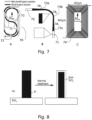
- the waveguide 33 is wound as a double spiral having counter-propagating counter clock-wise and clock-wise branches 34 and 35 respectively.
- Each opposite linear section 36a, 36b of the same turn is combined with bent sections 37a, 37b, each providing a phase-shift that compensates for the cancellation of Faraday rotation between counter-propagating waves in adjacent parallel linear sections of the waveguide, in the same manner as in Fig. 3A .
- FIG. 4 is shown in more detail a spiral for Faraday rotation
- Fig. 5 shows an experimental setup for a spiral with birefringent bends.
- a study on an integrated silicon Faraday rotator operating at 1.55 ⁇ m wavelength is now discussed, with reference to Figs. 4 and 5 .
- ⁇ ⁇ 2 ⁇ 2 + ⁇ / 2 _ 2
- ⁇ the mismatch of propagation constants between the TE- and TM-mode
- ⁇ the coupling constant between the two modes, which is for strong mode overlap equal to the Faraday rotation given in rad/m.
- the first problem can be mitigated by increasing the magnetic biasing field and thereby increasing ⁇ .
- both problems can be resolved by suppressing the unwanted birefringence. If the birefringence is due to shape inaccuracies the aspect ratio of the square cross-section can be altered with a thin conformal coating done with atomic layer deposition. The strain birefringence can thus be reduced by suppressing the birefringence in the linear section of the spiral, e.g. by thermally tuning the device.
- d ⁇ dT is -5( m ⁇ K ) -1 .
- This means one can compensate for a change in width of: 500 1 / m ⁇ d ⁇ d width ⁇ 1 2.66 nm .
- Larger errors in width can be compensated by oxidizing the outer part of the waveguide. For this approach, one may omit the silica top cladding in the bend and oxidize the surface of the waveguide, see Fig. 8 .
- Fig. 10 shows an alternative approach to avoid cancellation of the Faraday rotation, based on making the magnetic field B to bend or follow the waveguide spiral shape on a chip 93.
- it could be realized with a simple electric wire 94, but as strong magnetic fields in the order of 1 Tesla are needed for this practical Faraday rotation, it would be difficult to achieve with a single wire.
- a more promising approach is shown in Fig. 11 , where a toroidal wire 95 and an iron core 96 extending to the outside of the toroid, to come as close as possible to the waveguides.
- the spiral waveguide could also be sandwiched between two such electromagnets.
Landscapes
- Physics & Mathematics (AREA)
- Nonlinear Science (AREA)
- General Physics & Mathematics (AREA)
- Optics & Photonics (AREA)
- Engineering & Computer Science (AREA)
- Power Engineering (AREA)
- Microelectronics & Electronic Packaging (AREA)
- Optical Modulation, Optical Deflection, Nonlinear Optics, Optical Demodulation, Optical Logic Elements (AREA)
- Optical Integrated Circuits (AREA)
Claims (13)
- Optische Wellenleiterkomponente (30, 33) zum Bereitstellen einer Faraday-Rotation einer Polarisationsebene von linear polarisiertem Licht, das sich in der Wellenleiterkomponente (30, 33) ausbreitet, wobei die Wellenleiterkomponente (30, 33) aus Silizium hergestellt ist und gefaltete oder gewickelte Abschnitte (73) aufweist, die parallel zu einem von außen angelegten Magnetfeld verlaufen, wobei die Wellenleiterkomponente (30, 33) doppelbrechende gebogene Abschnitte (32, 37a, 37b) umfasst, dadurch gekennzeichnet, dass die doppelbrechenden gebogenen Abschnitte Biegungen basierend auf Totalinnenreflexionsspiegeln umfassen, um einen minimalen Platzbedarf zu erreichen.
- Optische Wellenleiterkomponente (33) nach Anspruch 1, wobei die Wellenleiterkomponente (33) als Spirale auf einer Ebene der Komponente (33) gewickelt ist.
- Optische Wellenleiterkomponente (30) nach Anspruch 1, wobei die Wellenleiterkomponente (30) in Mäanderform auf einer Ebene der Komponente (30) gewickelt ist, wodurch benachbarte lineare Abschnitte (31a, 31b), die parallel zueinander sind, mit gebogenen Abschnitten (32) der Wellenleiterkomponente (30) kombiniert sind, wobei die gebogenen Abschnitte (32) eine Phasenverschiebung zwischen parallelen Abschnitten (31a, 31b) mit gegenläufigem Licht bereitstellen, welche die Aufhebung von Faraday-Rotation zwischen gegenläufigen Wellen kompensiert.
- Optische Wellenleiterkomponente (33) nach Anspruch 2, wobei die Wellenleiterkomponente (33) als Doppelspirale gewickelt ist, die gegen den Uhrzeigersinn und im Uhrzeigersinn gegenläufige Zweige (34, 35) aufweist, wodurch gegenüberliegende lineare Wellenleiterabschnitte (36a, 36b) derselben Windung mit gebogenen Abschnitten (37a, 37b) der Wellenleiterkomponente (33) kombiniert sind, wobei jeder von dem gebogenen Abschnitt (37a, 37b) eine Phasenverschiebung bereitstellt, welche die Aufhebung von Faraday-Rotation zwischen gegenläufigen Wellen in dem gegenüberliegenden parallelen linearen Abschnitt (36a, 36b) derselben Windung des Wellenleiters kompensiert.
- Optische Wellenleiterkomponente (33) nach Anspruch 2, wobei die Wellenleiterkomponente (33) als eine einzelne Spirale gewickelt ist, die einen gegen den Uhrzeigersinn oder im Uhrzeigersinn verlaufenden Zweig (34, 35) aufweist.
- Optische Wellenleiterkomponente (30, 33) nach einem der Ansprüche 1-5, wobei die Wellenleiterkomponente (30, 33) abwechselnde lineare Abschnitte (31a, 31b, 36a, 36b) und gebogene Abschnitte (32, 37a, 37b) umfasst, wobei die linearen Abschnitte (31a, 31b, 36a, 36b) aus nicht doppelbrechendem Wellenleitermaterial bestehen und die gebogenen Abschnitte (32, 37a, 37b) aus doppelbrechendem Wellenleitermaterial bestehen, das eine Phasenverschiebung von 180° zwischen gegenläufigen Abschnitten (31a, 31b, 36a, 36b) bereitstellt.
- Optische Wellenleiterkomponente (30, 33) nach einem der Ansprüche 1-6, wobei das linear polarisierte Licht aus den grundlegenden transversalen elektrischen und transversalen magnetischen Moden besteht.
- Optische Wellenleiterkomponente (30, 33) nach einem der Ansprüche 1-7, wobei doppelbrechende gebogene Abschnitte (32, 37a, 37b) der Wellenleiterkomponente (30, 33) Biegungen mit einer zunehmenden Krümmung in der Ausbreitungsrichtung, wie etwa Eulersche Knicke umfassen.
- Optische Wellenleiterkomponente (30, 33) nach einem der Ansprüche 1-8, wobei die Doppelbrechung eines optischen Wellenleiterabschnitts durch thermische Oxidation des Siliziummaterials in dem Wellenleiterabschnitt gesteuert wird.
- Optische Wellenleiterkomponente (30, 33) nach einem der Ansprüche 1-9, wobei die Doppelbrechung eines optischen Wellenleiterabschnitts durch Ätzen des Siliziummaterials in dem Wellenleiterabschnitt gesteuert wird.
- Optische Wellenleiterkomponente (30, 33) nach einem der Ansprüche 1-10, wobei die Doppelbrechung eines optischen Wellenleiterabschnitts durch die Abscheidung einer Mantelschicht, z. B. Si3N4, gesteuert wird, um in dem Wellenleiterabschnitt Spannung zu induzieren.
- Optische Wellenleiterkomponente nach einem der Ansprüche 1-11, wobei die Doppelbrechung eines optischen Wellenleiterabschnitts durch eine Atomlagenabscheidung (ALD) gesteuert wird,
- Optische Wellenleiterkomponente (30, 33) nach einem der Ansprüche 1-12, wobei die Doppelbrechung eines optischen Wellenleiterabschnitts durch die Abscheidung piezoelektrischer Materialien zur aktiven Steuerung der Spannung in dem Wellenleiterabschnitt gesteuert wird.
Applications Claiming Priority (2)
| Application Number | Priority Date | Filing Date | Title |
|---|---|---|---|
| US201762548467P | 2017-08-22 | 2017-08-22 | |
| PCT/FI2018/050595 WO2019038477A1 (en) | 2017-08-22 | 2018-08-22 | INTEGRATED FARADAY ROTATOR |
Publications (4)
| Publication Number | Publication Date |
|---|---|
| EP3673325A1 EP3673325A1 (de) | 2020-07-01 |
| EP3673325A4 EP3673325A4 (de) | 2021-05-05 |
| EP3673325B1 true EP3673325B1 (de) | 2024-11-20 |
| EP3673325C0 EP3673325C0 (de) | 2024-11-20 |
Family
ID=65439972
Family Applications (1)
| Application Number | Title | Priority Date | Filing Date |
|---|---|---|---|
| EP18848653.4A Active EP3673325B1 (de) | 2017-08-22 | 2018-08-22 | Integriertes faraday-drehgelenk |
Country Status (5)
| Country | Link |
|---|---|
| US (1) | US11506919B2 (de) |
| EP (1) | EP3673325B1 (de) |
| JP (1) | JP2020531910A (de) |
| CN (1) | CN111247478A (de) |
| WO (1) | WO2019038477A1 (de) |
Families Citing this family (5)
| Publication number | Priority date | Publication date | Assignee | Title |
|---|---|---|---|---|
| US11275210B1 (en) | 2018-12-07 | 2022-03-15 | PsiQuantum Corp. | Waveguide couplers for multi-mode waveguides |
| US11635570B1 (en) | 2019-02-08 | 2023-04-25 | PsiQuantum Corp. | Multi-mode multi-pass delay |
| US11391890B1 (en) * | 2019-05-15 | 2022-07-19 | PsiQuantum Corp. | Multi-mode spiral delay device |
| US11886058B2 (en) * | 2019-05-24 | 2024-01-30 | Rockley Photonics Limited | Optical isolator |
| JPWO2024048747A1 (de) * | 2022-08-31 | 2024-03-07 |
Citations (7)
| Publication number | Priority date | Publication date | Assignee | Title |
|---|---|---|---|---|
| US4733938A (en) * | 1981-11-09 | 1988-03-29 | The Board Of Trustees Of The Leland Stanford Junior University | Magneto-optic rotator |
| US20030206681A1 (en) * | 2002-05-02 | 2003-11-06 | Vyoptics, Inc. | Integrating element for optical fiber communication systems based on photonic multi-bandgap quasi-crystals having optimized transfer functions |
| US20050275944A1 (en) * | 2004-06-11 | 2005-12-15 | Wang Jian J | Optical films and methods of making the same |
| JP2007155967A (ja) * | 2005-12-02 | 2007-06-21 | Nippon Telegr & Teleph Corp <Ntt> | 電磁波偏波面回転装置 |
| US20070147725A1 (en) * | 2003-04-30 | 2007-06-28 | Paolo Crespi | Coupled-waveguide electro-optic switch based on polarisation conversion |
| US20140217269A1 (en) * | 2013-02-01 | 2014-08-07 | The Board Of Trustees Of The Leland Stanford Junior University | Coupled waveguides for slow light sensor applications |
| US20160011438A1 (en) * | 2013-02-25 | 2016-01-14 | Ohio State Innovation Foundation | On-chip optical polarization controller |
Family Cites Families (8)
| Publication number | Priority date | Publication date | Assignee | Title |
|---|---|---|---|---|
| US4615582A (en) * | 1981-11-09 | 1986-10-07 | The Board Of Trustees Of The Leland Stanford Junior University | Magneto-optic rotator for providing additive Faraday rotations in a loop of optical fiber |
| US6738396B2 (en) * | 2001-07-24 | 2004-05-18 | Gsi Lumonics Ltd. | Laser based material processing methods and scalable architecture for material processing |
| JP3979138B2 (ja) * | 2001-12-20 | 2007-09-19 | 住友電気工業株式会社 | 光アイソレータおよび偏光子 |
| US20030202770A1 (en) | 2002-01-03 | 2003-10-30 | Garito Anthony F. | Optical waveguide amplifiers |
| FI20020698A0 (fi) | 2002-04-11 | 2002-04-11 | Valtion Teknillinen | Integroidun optisen piirin valokanava ja menetelmä valokanavan valmistamiseksi |
| JP2009210797A (ja) * | 2008-03-04 | 2009-09-17 | Nippon Telegr & Teleph Corp <Ntt> | 電磁波偏波面回転装置 |
| US8837877B2 (en) | 2011-08-11 | 2014-09-16 | Massachusetts Institute Of Technology | Patterned non-reciprocal optical resonator |
| FI124843B (fi) * | 2012-10-18 | 2015-02-13 | Teknologian Tutkimuskeskus Vtt | Taivutettu optinen aaltojohde |
-
2018
- 2018-08-22 CN CN201880054922.7A patent/CN111247478A/zh active Pending
- 2018-08-22 EP EP18848653.4A patent/EP3673325B1/de active Active
- 2018-08-22 JP JP2020511226A patent/JP2020531910A/ja active Pending
- 2018-08-22 WO PCT/FI2018/050595 patent/WO2019038477A1/en not_active Ceased
- 2018-08-22 US US16/640,736 patent/US11506919B2/en active Active
Patent Citations (7)
| Publication number | Priority date | Publication date | Assignee | Title |
|---|---|---|---|---|
| US4733938A (en) * | 1981-11-09 | 1988-03-29 | The Board Of Trustees Of The Leland Stanford Junior University | Magneto-optic rotator |
| US20030206681A1 (en) * | 2002-05-02 | 2003-11-06 | Vyoptics, Inc. | Integrating element for optical fiber communication systems based on photonic multi-bandgap quasi-crystals having optimized transfer functions |
| US20070147725A1 (en) * | 2003-04-30 | 2007-06-28 | Paolo Crespi | Coupled-waveguide electro-optic switch based on polarisation conversion |
| US20050275944A1 (en) * | 2004-06-11 | 2005-12-15 | Wang Jian J | Optical films and methods of making the same |
| JP2007155967A (ja) * | 2005-12-02 | 2007-06-21 | Nippon Telegr & Teleph Corp <Ntt> | 電磁波偏波面回転装置 |
| US20140217269A1 (en) * | 2013-02-01 | 2014-08-07 | The Board Of Trustees Of The Leland Stanford Junior University | Coupled waveguides for slow light sensor applications |
| US20160011438A1 (en) * | 2013-02-25 | 2016-01-14 | Ohio State Innovation Foundation | On-chip optical polarization controller |
Non-Patent Citations (2)
| Title |
|---|
| MATTEO CHERCHI ET AL: "Dramatic size reduction of waveguide bends on a micron-scale silicon photonic platform", OPTICS EXPRESS, vol. 21, no. 15, 18 July 2013 (2013-07-18), pages 17814, XP055253507, DOI: 10.1364/OE.21.017814 * |
| MORICHETTI FRANCESCO ET AL: "Modelling of Polarization Rotation in Bent Waveguides", 8TH INTERNATIONAL CONFERENCE ON TRANSPARENT OPTICAL NETWORKS - ICTON 2006. NOTTINGHAM, UNITED KINGDOM, JUNE 18-22, 2006, 18 June 2006 (2006-06-18), pages 261 - 261, XP093040031, ISBN: 978-1-4244-0236-6, Retrieved from the Internet <URL:https://ieeexplore.ieee.org/stampPDF/getPDF.jsp?tp=&arnumber=4013918&ref=aHR0cHM6Ly93d3cuZ29vZ2xlLmNvbS8=> DOI: 10.1109/ICTON.2006.248464 * |
Also Published As
| Publication number | Publication date |
|---|---|
| US20200192134A1 (en) | 2020-06-18 |
| CN111247478A (zh) | 2020-06-05 |
| EP3673325A4 (de) | 2021-05-05 |
| US11506919B2 (en) | 2022-11-22 |
| WO2019038477A1 (en) | 2019-02-28 |
| JP2020531910A (ja) | 2020-11-05 |
| EP3673325A1 (de) | 2020-07-01 |
| EP3673325C0 (de) | 2024-11-20 |
Similar Documents
| Publication | Publication Date | Title |
|---|---|---|
| EP3673325B1 (de) | Integriertes faraday-drehgelenk | |
| Bi et al. | On-chip optical isolation in monolithically integrated non-reciprocal optical resonators | |
| Shoji et al. | Optical nonreciprocal devices based on magneto-optical phase shift in silicon photonics | |
| US9075251B2 (en) | Integrated photonic devices with reduced sensitivity to external influences | |
| US20100238536A1 (en) | Integrated silicon/silicon-germanium magneto-optic isolator | |
| US8837877B2 (en) | Patterned non-reciprocal optical resonator | |
| US20080267557A1 (en) | Integrated Magneto-Optical Devices for Uni-Directional Optical Resonator Systems | |
| EP1980895A1 (de) | Optischer isolator | |
| Mitsuya et al. | Demonstration of a silicon waveguide optical circulator | |
| Shahwar et al. | Polarization management in silicon photonics | |
| Jalas et al. | Faraday rotation in silicon waveguides | |
| Heidari et al. | Design and analysis of a graphene magneto-plasmon waveguide for plasmonic mode switch | |
| Kono et al. | A novel finite-element method for nonreciprocal magneto-photonic crystal waveguides | |
| Takei et al. | Design and simulation of silicon waveguide optical circulator employing nonreciprocal phase shift | |
| JP5223092B2 (ja) | 偏波無依存光アイソレータ | |
| Li et al. | Compact and low loss magneto-optical waveguide isolator for TE mode based on lithium niobate on insulator | |
| Abadian et al. | Integrated magneto-plasmonic isolation enhancement based on coupled resonances in subwavelength gold grating | |
| Bouchemat et al. | Mode conversion in magneto photonic crystal fibre | |
| Tummidi et al. | An ultra-compact waveguide polarizer based on “anti-magic widths” | |
| US20250123507A1 (en) | Phase-matched nonreciprocal polarization rotating waveguide device and optical isolator/optical circulator using thereof | |
| US20120057819A1 (en) | Photonic devices having degenerate or split spectral band edges and methods for using the same | |
| KR102898220B1 (ko) | 편광 모드 제어형 비가역 광 도파로 소자 및 이를 이용한 광 아이솔레이터 및 광 서큘레이터 소자 | |
| Mizumoto et al. | Silicon waveguide optical nonreciprocal devices based on magneto-optical phase shift | |
| Xu et al. | Polarization-insensitive MMI-coupled ring resonators in silicon-on-insulator using cladding stress engineering | |
| CN120010142B (zh) | 一种基于磁性光子晶体光纤的光隔离器 |
Legal Events
| Date | Code | Title | Description |
|---|---|---|---|
| STAA | Information on the status of an ep patent application or granted ep patent |
Free format text: STATUS: THE INTERNATIONAL PUBLICATION HAS BEEN MADE |
|
| PUAI | Public reference made under article 153(3) epc to a published international application that has entered the european phase |
Free format text: ORIGINAL CODE: 0009012 |
|
| STAA | Information on the status of an ep patent application or granted ep patent |
Free format text: STATUS: REQUEST FOR EXAMINATION WAS MADE |
|
| 17P | Request for examination filed |
Effective date: 20200219 |
|
| AK | Designated contracting states |
Kind code of ref document: A1 Designated state(s): AL AT BE BG CH CY CZ DE DK EE ES FI FR GB GR HR HU IE IS IT LI LT LU LV MC MK MT NL NO PL PT RO RS SE SI SK SM TR |
|
| AX | Request for extension of the european patent |
Extension state: BA ME |
|
| DAV | Request for validation of the european patent (deleted) | ||
| DAX | Request for extension of the european patent (deleted) | ||
| A4 | Supplementary search report drawn up and despatched |
Effective date: 20210409 |
|
| RIC1 | Information provided on ipc code assigned before grant |
Ipc: G02F 1/095 20060101AFI20210401BHEP Ipc: G02B 6/125 20060101ALI20210401BHEP Ipc: G02B 6/126 20060101ALI20210401BHEP |
|
| STAA | Information on the status of an ep patent application or granted ep patent |
Free format text: STATUS: EXAMINATION IS IN PROGRESS |
|
| 17Q | First examination report despatched |
Effective date: 20230425 |
|
| GRAP | Despatch of communication of intention to grant a patent |
Free format text: ORIGINAL CODE: EPIDOSNIGR1 |
|
| STAA | Information on the status of an ep patent application or granted ep patent |
Free format text: STATUS: GRANT OF PATENT IS INTENDED |
|
| RIC1 | Information provided on ipc code assigned before grant |
Ipc: G02B 6/126 20060101ALI20240521BHEP Ipc: G02F 1/095 20060101AFI20240521BHEP |
|
| INTG | Intention to grant announced |
Effective date: 20240619 |
|
| GRAS | Grant fee paid |
Free format text: ORIGINAL CODE: EPIDOSNIGR3 |
|
| GRAA | (expected) grant |
Free format text: ORIGINAL CODE: 0009210 |
|
| STAA | Information on the status of an ep patent application or granted ep patent |
Free format text: STATUS: THE PATENT HAS BEEN GRANTED |
|
| RAP3 | Party data changed (applicant data changed or rights of an application transferred) |
Owner name: TEKNOLOGIAN TUTKIMUSKESKUS VTT OY |
|
| RIN1 | Information on inventor provided before grant (corrected) |
Inventor name: EICH, MANFRED Inventor name: AALTO, TIMO Inventor name: HARJANNE, MIKKO Inventor name: JALAS, DIRK Inventor name: PETROV, ALEXANDER Inventor name: CHERCHI, MATTEO |
|
| AK | Designated contracting states |
Kind code of ref document: B1 Designated state(s): AL AT BE BG CH CY CZ DE DK EE ES FI FR GB GR HR HU IE IS IT LI LT LU LV MC MK MT NL NO PL PT RO RS SE SI SK SM TR |
|
| REG | Reference to a national code |
Ref country code: GB Ref legal event code: FG4D |
|
| REG | Reference to a national code |
Ref country code: CH Ref legal event code: EP |
|
| REG | Reference to a national code |
Ref country code: DE Ref legal event code: R096 Ref document number: 602018076811 Country of ref document: DE |
|
| REG | Reference to a national code |
Ref country code: IE Ref legal event code: FG4D |
|
| U01 | Request for unitary effect filed |
Effective date: 20241121 |
|
| U07 | Unitary effect registered |
Designated state(s): AT BE BG DE DK EE FI FR IT LT LU LV MT NL PT RO SE SI Effective date: 20241127 |
|
| PG25 | Lapsed in a contracting state [announced via postgrant information from national office to epo] |
Ref country code: HR Free format text: LAPSE BECAUSE OF FAILURE TO SUBMIT A TRANSLATION OF THE DESCRIPTION OR TO PAY THE FEE WITHIN THE PRESCRIBED TIME-LIMIT Effective date: 20241120 Ref country code: IS Free format text: LAPSE BECAUSE OF FAILURE TO SUBMIT A TRANSLATION OF THE DESCRIPTION OR TO PAY THE FEE WITHIN THE PRESCRIBED TIME-LIMIT Effective date: 20250320 |
|
| PG25 | Lapsed in a contracting state [announced via postgrant information from national office to epo] |
Ref country code: ES Free format text: LAPSE BECAUSE OF FAILURE TO SUBMIT A TRANSLATION OF THE DESCRIPTION OR TO PAY THE FEE WITHIN THE PRESCRIBED TIME-LIMIT Effective date: 20241120 |
|
| PG25 | Lapsed in a contracting state [announced via postgrant information from national office to epo] |
Ref country code: NO Free format text: LAPSE BECAUSE OF FAILURE TO SUBMIT A TRANSLATION OF THE DESCRIPTION OR TO PAY THE FEE WITHIN THE PRESCRIBED TIME-LIMIT Effective date: 20250220 |
|
| PG25 | Lapsed in a contracting state [announced via postgrant information from national office to epo] |
Ref country code: GR Free format text: LAPSE BECAUSE OF FAILURE TO SUBMIT A TRANSLATION OF THE DESCRIPTION OR TO PAY THE FEE WITHIN THE PRESCRIBED TIME-LIMIT Effective date: 20250221 |
|
| PG25 | Lapsed in a contracting state [announced via postgrant information from national office to epo] |
Ref country code: PL Free format text: LAPSE BECAUSE OF FAILURE TO SUBMIT A TRANSLATION OF THE DESCRIPTION OR TO PAY THE FEE WITHIN THE PRESCRIBED TIME-LIMIT Effective date: 20241120 |
|
| PG25 | Lapsed in a contracting state [announced via postgrant information from national office to epo] |
Ref country code: RS Free format text: LAPSE BECAUSE OF FAILURE TO SUBMIT A TRANSLATION OF THE DESCRIPTION OR TO PAY THE FEE WITHIN THE PRESCRIBED TIME-LIMIT Effective date: 20250220 |
|
| PG25 | Lapsed in a contracting state [announced via postgrant information from national office to epo] |
Ref country code: SM Free format text: LAPSE BECAUSE OF FAILURE TO SUBMIT A TRANSLATION OF THE DESCRIPTION OR TO PAY THE FEE WITHIN THE PRESCRIBED TIME-LIMIT Effective date: 20241120 |
|
| PG25 | Lapsed in a contracting state [announced via postgrant information from national office to epo] |
Ref country code: SK Free format text: LAPSE BECAUSE OF FAILURE TO SUBMIT A TRANSLATION OF THE DESCRIPTION OR TO PAY THE FEE WITHIN THE PRESCRIBED TIME-LIMIT Effective date: 20241120 |
|
| PG25 | Lapsed in a contracting state [announced via postgrant information from national office to epo] |
Ref country code: CZ Free format text: LAPSE BECAUSE OF FAILURE TO SUBMIT A TRANSLATION OF THE DESCRIPTION OR TO PAY THE FEE WITHIN THE PRESCRIBED TIME-LIMIT Effective date: 20241120 |
|
| PLBE | No opposition filed within time limit |
Free format text: ORIGINAL CODE: 0009261 |
|
| STAA | Information on the status of an ep patent application or granted ep patent |
Free format text: STATUS: NO OPPOSITION FILED WITHIN TIME LIMIT |
|
| U20 | Renewal fee for the european patent with unitary effect paid |
Year of fee payment: 8 Effective date: 20250827 |
|
| PGFP | Annual fee paid to national office [announced via postgrant information from national office to epo] |
Ref country code: GB Payment date: 20250820 Year of fee payment: 8 |
|
| 26N | No opposition filed |
Effective date: 20250821 |