EP3671720B1 - Real-time on-chip data transfer system - Google Patents
Real-time on-chip data transfer system Download PDFInfo
- Publication number
- EP3671720B1 EP3671720B1 EP19210427.1A EP19210427A EP3671720B1 EP 3671720 B1 EP3671720 B1 EP 3671720B1 EP 19210427 A EP19210427 A EP 19210427A EP 3671720 B1 EP3671720 B1 EP 3671720B1
- Authority
- EP
- European Patent Office
- Prior art keywords
- payload
- csi
- data
- loopback
- signal
- Prior art date
- Legal status (The legal status is an assumption and is not a legal conclusion. Google has not performed a legal analysis and makes no representation as to the accuracy of the status listed.)
- Active
Links
- 238000012546 transfer Methods 0.000 title claims description 16
- 239000000872 buffer Substances 0.000 claims description 163
- 230000005540 biological transmission Effects 0.000 claims description 33
- 238000000034 method Methods 0.000 claims description 20
- 238000012937 correction Methods 0.000 claims description 11
- 230000004044 response Effects 0.000 claims description 10
- 230000001172 regenerating effect Effects 0.000 claims description 3
- 238000012856 packing Methods 0.000 claims description 2
- 230000007704 transition Effects 0.000 description 38
- 238000010586 diagram Methods 0.000 description 19
- 230000011664 signaling Effects 0.000 description 8
- 230000001934 delay Effects 0.000 description 6
- 230000000977 initiatory effect Effects 0.000 description 4
- 238000012360 testing method Methods 0.000 description 4
- 238000012545 processing Methods 0.000 description 2
- 230000001360 synchronised effect Effects 0.000 description 2
- 230000003139 buffering effect Effects 0.000 description 1
- 125000004122 cyclic group Chemical group 0.000 description 1
- 230000006870 function Effects 0.000 description 1
- 238000005259 measurement Methods 0.000 description 1
- 238000012986 modification Methods 0.000 description 1
- 230000004048 modification Effects 0.000 description 1
Images


Classifications
-
- G—PHYSICS
- G09—EDUCATION; CRYPTOGRAPHY; DISPLAY; ADVERTISING; SEALS
- G09G—ARRANGEMENTS OR CIRCUITS FOR CONTROL OF INDICATING DEVICES USING STATIC MEANS TO PRESENT VARIABLE INFORMATION
- G09G3/00—Control arrangements or circuits, of interest only in connection with visual indicators other than cathode-ray tubes
- G09G3/006—Electronic inspection or testing of displays and display drivers, e.g. of LED or LCD displays
-
- H—ELECTRICITY
- H04—ELECTRIC COMMUNICATION TECHNIQUE
- H04L—TRANSMISSION OF DIGITAL INFORMATION, e.g. TELEGRAPHIC COMMUNICATION
- H04L49/00—Packet switching elements
- H04L49/90—Buffering arrangements
- H04L49/9042—Separate storage for different parts of the packet, e.g. header and payload
-
- G—PHYSICS
- G06—COMPUTING; CALCULATING OR COUNTING
- G06F—ELECTRIC DIGITAL DATA PROCESSING
- G06F3/00—Input arrangements for transferring data to be processed into a form capable of being handled by the computer; Output arrangements for transferring data from processing unit to output unit, e.g. interface arrangements
- G06F3/14—Digital output to display device ; Cooperation and interconnection of the display device with other functional units
- G06F3/147—Digital output to display device ; Cooperation and interconnection of the display device with other functional units using display panels
-
- G—PHYSICS
- G09—EDUCATION; CRYPTOGRAPHY; DISPLAY; ADVERTISING; SEALS
- G09G—ARRANGEMENTS OR CIRCUITS FOR CONTROL OF INDICATING DEVICES USING STATIC MEANS TO PRESENT VARIABLE INFORMATION
- G09G5/00—Control arrangements or circuits for visual indicators common to cathode-ray tube indicators and other visual indicators
- G09G5/003—Details of a display terminal, the details relating to the control arrangement of the display terminal and to the interfaces thereto
- G09G5/006—Details of the interface to the display terminal
-
- G—PHYSICS
- G09—EDUCATION; CRYPTOGRAPHY; DISPLAY; ADVERTISING; SEALS
- G09G—ARRANGEMENTS OR CIRCUITS FOR CONTROL OF INDICATING DEVICES USING STATIC MEANS TO PRESENT VARIABLE INFORMATION
- G09G5/00—Control arrangements or circuits for visual indicators common to cathode-ray tube indicators and other visual indicators
- G09G5/36—Control arrangements or circuits for visual indicators common to cathode-ray tube indicators and other visual indicators characterised by the display of a graphic pattern, e.g. using an all-points-addressable [APA] memory
- G09G5/39—Control of the bit-mapped memory
- G09G5/395—Arrangements specially adapted for transferring the contents of the bit-mapped memory to the screen
-
- H—ELECTRICITY
- H04—ELECTRIC COMMUNICATION TECHNIQUE
- H04L—TRANSMISSION OF DIGITAL INFORMATION, e.g. TELEGRAPHIC COMMUNICATION
- H04L49/00—Packet switching elements
- H04L49/30—Peripheral units, e.g. input or output ports
- H04L49/3063—Pipelined operation
-
- H—ELECTRICITY
- H04—ELECTRIC COMMUNICATION TECHNIQUE
- H04L—TRANSMISSION OF DIGITAL INFORMATION, e.g. TELEGRAPHIC COMMUNICATION
- H04L49/00—Packet switching elements
- H04L49/55—Prevention, detection or correction of errors
- H04L49/552—Prevention, detection or correction of errors by ensuring the integrity of packets received through redundant connections
-
- H—ELECTRICITY
- H04—ELECTRIC COMMUNICATION TECHNIQUE
- H04L—TRANSMISSION OF DIGITAL INFORMATION, e.g. TELEGRAPHIC COMMUNICATION
- H04L49/00—Packet switching elements
- H04L49/90—Buffering arrangements
- H04L49/901—Buffering arrangements using storage descriptor, e.g. read or write pointers
-
- H—ELECTRICITY
- H04—ELECTRIC COMMUNICATION TECHNIQUE
- H04L—TRANSMISSION OF DIGITAL INFORMATION, e.g. TELEGRAPHIC COMMUNICATION
- H04L7/00—Arrangements for synchronising receiver with transmitter
- H04L7/02—Speed or phase control by the received code signals, the signals containing no special synchronisation information
- H04L7/033—Speed or phase control by the received code signals, the signals containing no special synchronisation information using the transitions of the received signal to control the phase of the synchronising-signal-generating means, e.g. using a phase-locked loop
- H04L7/0331—Speed or phase control by the received code signals, the signals containing no special synchronisation information using the transitions of the received signal to control the phase of the synchronising-signal-generating means, e.g. using a phase-locked loop with a digital phase-locked loop [PLL] processing binary samples, e.g. add/subtract logic for correction of receiver clock
-
- H—ELECTRICITY
- H04—ELECTRIC COMMUNICATION TECHNIQUE
- H04N—PICTORIAL COMMUNICATION, e.g. TELEVISION
- H04N5/00—Details of television systems
- H04N5/04—Synchronising
- H04N5/06—Generation of synchronising signals
- H04N5/067—Arrangements or circuits at the transmitter end
-
- G—PHYSICS
- G09—EDUCATION; CRYPTOGRAPHY; DISPLAY; ADVERTISING; SEALS
- G09G—ARRANGEMENTS OR CIRCUITS FOR CONTROL OF INDICATING DEVICES USING STATIC MEANS TO PRESENT VARIABLE INFORMATION
- G09G2320/00—Control of display operating conditions
- G09G2320/06—Adjustment of display parameters
- G09G2320/0693—Calibration of display systems
-
- G—PHYSICS
- G09—EDUCATION; CRYPTOGRAPHY; DISPLAY; ADVERTISING; SEALS
- G09G—ARRANGEMENTS OR CIRCUITS FOR CONTROL OF INDICATING DEVICES USING STATIC MEANS TO PRESENT VARIABLE INFORMATION
- G09G2330/00—Aspects of power supply; Aspects of display protection and defect management
- G09G2330/12—Test circuits or failure detection circuits included in a display system, as permanent part thereof
-
- G—PHYSICS
- G09—EDUCATION; CRYPTOGRAPHY; DISPLAY; ADVERTISING; SEALS
- G09G—ARRANGEMENTS OR CIRCUITS FOR CONTROL OF INDICATING DEVICES USING STATIC MEANS TO PRESENT VARIABLE INFORMATION
- G09G2370/00—Aspects of data communication
- G09G2370/10—Use of a protocol of communication by packets in interfaces along the display data pipeline
Definitions
- the present invention relates generally to system-on-chips (SoCs) with high-speed serial interfaces, and, more particularly, to a system for transferring data between two high speed serial interfaces on a SoC.
- SoCs system-on-chips
- SoCs have two or more high-speed serial interfaces (HSSIs), and in certain scenarios, it is desirable to transfer data from the pads of one HSSI directly to the other HSSI.
- HSSIs high-speed serial interfaces
- MIPI-CSI2 Mobile Industry Processor Interface - Camera Serial Interface
- MIPI-CSI2 Mobile Industry Processor Interface - Camera Serial Interface
- MIPI-CSI2 Mobile Industry Processor Interface - Camera Serial Interface
- MIPI-CSI2 Mobile Industry Processor Interface - Camera Serial Interface
- US 2017/0201746 A1 discloses a system on chip including a display serial interface host device, a camera serial interface host device, a first register and a loopback control circuit, the first register configured to store a first flag indicating whether the system on chip is operating in a loopback mode or a non-loopback mode.
- the MIPI Alliance Specification for M-PHY, Version 1.00.00, 8 February 2011 discloses a serial interface technology with high bandwidth capabilities, developed in particular for mobile applications.
- US 2009/315899 A1 discloses a graphics multi-media integrated circuit connected to a host processor over two serial links: a half duplex bi-directional serial link which accords to a protocol defined for a display serial interface, and a uni-directional serial link which accords to a compatible protocol defined for a camera serial interface.
- a system-on-chip having two or more high-speed serial interfaces
- the SoC comprising: a camera serial interface (CSI) receiver adapted to receive sensor data via a first serial interface and to generate a data packet that includes a payload; a loopback buffer connected to the CSI receiver, wherein the CSI receiver is adapted to write the payload into the loopback buffer; and a CSI transmitter connected between a second serial interface and the loopback buffer, characterized in that:
- the CSI receiver may comprises: a first digital physical layer (DPHY) connected to an external camera sensor by way of the first interface for receiving the sensor data and a first clock signal, wherein the first DPHY outputs the sensor data, and generates active, sync, and valid signals, wherein the active signal is generated when the first DPHY is ready to transmit the sensor data, the sync signal is generated to synchronize a transmission frequency of the sensor data with a frequency of the first clock signal, and the valid signal is generated when the sensor data is valid; a first CSI controller connected to the first DPHY for receiving the sensor data and the active, sync, and valid signals, wherein the first CSI controller (i) generates the data packet, (ii) separates the payload and the packet header, (iii) outputs the payload and the packet header, (iv) performs error correction on the data packet to generate an error signal, and (v) generates an end of packet (EOP) signal, wherein the error signal indicates an error in the data packet
- the first loopback controller may comprise: an error handler connected to the first CSI controller for receiving the packet header, the payload, the EOP signal, and the error signal, and outputting the packet header, the EOP signal, and the payload, wherein the error handler outputs the packet header and the payload when the error signal indicates that the data packet does not include an error; a first pipeline controller connected to the error handler for receiving the packet header and the EOP signal, wherein the first pipeline controller (i) decodes the type of the data packet from the packet header, (ii) outputs the packet header and the EOP signal, and (iii) generates a write control signal, wherein the first pipeline controller receives the EOP signal from the error handler when the error handler receives the complete payload; a first buffer connected to the first pipeline controller for receiving the packet header and the EOP signal, wherein the first buffer provides the packet header and the EOP signal to the CSI transmitter; a data formatter connected to the error handler and the first pipeline controller for receiving
- the CSI transmitter may comprise: a second loopback controller connected to the first loopback controller for reading the packet header, and receiving the EOP signal, wherein the second loopback controller also is connected to the loopback buffer for receiving the formatted payload, wherein the second loopback controller (i) unpacks the formatted payload to regenerate the payload and (ii) output the packet header; a second CSI controller connected to the second loopback controller for receiving the packet header and the payload, wherein the second CSI controller combines the packet header and the payload to regenerate the data packet and generates loopback data and a request signal for requesting high speed transmission of the loopback data, wherein a format of the loopback data is the same as a format of the sensor data; a second DPHY that receives a second clock signal, and is connected to the second CSI controller for receiving the request signal and the loopback data, wherein the second DPHY transmits a ready signal to the second CSI controller and the second CSI controller provides the loopback data to the second
- the second loopback controller may comprise: a header read controller connected to the first buffer for reading the packet header and receiving the EOP signal, wherein the header read controller (i) identifies a size of the payload and (ii) outputs the packet header and payload size information; a second pipeline controller that receives a status signal, and is connected to the header read controller for receiving the packet header, wherein the second pipeline controller generates a read control signal; a data read controller connected to the header read controller, the second pipeline controller, and the loopback buffer for receiving the payload size information, the read control signal, and the formatted payload, respectively, and outputting the formatted payload, wherein the data read controller reads the formatted payload from the loopback buffer based on the size information and the read control signal; and a data un-formatter connected to the data read controller for receiving the formatted payload, wherein the data un-formatter (i) unpacks the formatted payload to regenerate the payload and (ii) generates the status signal, where
- the SoC may further comprise a primary system memory connected to the CSI receiver, wherein the CSI receiver writes the payload into the primary system memory.
- the CSI receiver may further comprise a system memory write interface connected to the first CSI controller for receiving the packet header, the payload, the EOP signal, and the error signal, wherein the CSI receiver writes the payload into the primary system memory.
- a method for data transfer in a system-on-chip that includes a camera serial interface (CSI) receiver connected to a first high-speed serial interface (HSSI), a loopback buffer, and a CSI transmitter connected to a second high-speed serial interface (HSSI), the method comprising:
- the method may further comprise: receiving, by the CSI receiver, sensor data and a first clock signal from an external camera sensor over the first HSSI; generating, by the CSI receiver, valid and sync signals, wherein the sync signal is generated to synchronize a transmission frequency of the sensor data with a frequency of the first clock signal, and the valid signal is generated when the sensor data is valid; performing, by the CSI receiver, error correction on the data packet; separating, by the CSI receiver, the packet header and the payload of the data packet; writing, by the CSI receiver, the payload into the loopback buffer; and transmitting, by the CSI receiver, the packet header to the CSI transmitter.
- the steps of writing the payload and transmitting the packet header may further comprise: decoding, by the CSI receiver, a type of the data packet from the packet header; packing, by the CSI receiver, the payload to generate a formatted payload when the type of the data packet is a long packet, wherein the payload written by the CSI receiver into the loopback buffer is the formatted payload; and communicating, by the CSI receiver, an end of packet (EOP) signal to the CSI transmitter, wherein the EOP signal indicates an end of the data packet.
- EOP end of packet
- the method may further comprise: reading, by the CSI transmitter, the formatted payload from the loopback buffer; regenerating, by the CSI transmitter, the payload; combining, by the CSI transmitter, the regenerated payload and the packet header to regenerate the data packet; generating, by the CSI transmitter, loopback data and a request signal for requesting high speed transmission of the loopback data, wherein the loopback data has the same format as the sensor data; generating, by the CSI transmitter, a ready signal in response to the request signal; and outputting the loopback data over the second HSSI by the CSI transmitter.
- the step of regenerating the payload may further comprise: identifying, by the CSI transmitter, a size of the payload; generating, by the CSI transmitter, a read control signal; reading, by the CSI transmitter, the formatted payload from the loopback buffer based on the size of the payload and the read control signal; and unpacking, by the CSI transmitter, the formatted payload to regenerate the payload.
- the method may further comprise writing, by the CSI receiver, the payload into a primary system memory of the SoC.
- SoC system-on-chip
- the CSI receiver receives sensor data and generates a data packet that includes a payload.
- the loopback buffer is connected to the CSI receiver.
- the CSI receiver writes the payload into the loopback buffer.
- the CSI transmitter is connected to the loopback buffer for reading the payload.
- the CSI transmitter reads the payload when at least one of a threshold capacity of the loopback buffer is reached and the payload is received completely by the loopback buffer.
- SoC system-on-chip
- the SoC includes a CSI receiver, a loopback buffer, and a CSI transmitter.
- the method includes generating a data packet that includes a payload and writing the payload to the loopback buffer.
- the method further includes reading the payload from the loopback buffer when at least one of a threshold capacity of the loopback buffer is reached and the payload is received completely by the loopback buffer.
- SoC system-on-chip
- the CSI receiver receives sensor data and generates a data packet that includes a payload.
- the loopback buffer is connected to the CSI receiver.
- the CSI receiver writes the payload into the loopback buffer.
- the CSI transmitter is connected to the loopback buffer for reading the payload.
- the CSI transmitter generates loopback data and reads the payload when at least one of a threshold capacity of the loopback buffer is reached and the payload is received completely by the loopback buffer.
- a format of the loopback data is the same as a format of the sensor data.
- Various embodiments of the present invention provide a method and system for transferring data between two high-speed serial interfaces (HSSI) in a SoC without using system memory.
- the SoC includes a CSI receiver connected to one HSSI, a loopback buffer, and a CSI transmitter connected to another HSSI.
- the CSI receiver receives raw sensor data from the first HSSI and generates a data packet including a header and a payload.
- the CSI receiver then writes the payload of the data packet into the loopback buffer.
- the CSI transmitter reads the payload from the loopback buffer when at least one of the threshold capacity is reached and the payload is received completely by the loopback buffer.
- the CSI transmitter also generates loopback data based on the amount of payload data read by the CSI transmitter.
- the sensor data and the loopback data both have the same format.
- the method and system eliminate the need to use system memory for data transfers between two HSSI. Further, as the loopback data and the sensor data have the same format, there is no need to convert the format of the loopback data to the format of the sensor data.
- system 100 a block diagram of a system for data transfer 100 (hereinafter referred to as "system 100"), in accordance with an embodiment of the present invention is shown.
- the system 100 may be implemented in integrated circuits like SoCs and used for automotive applications such as a connected car, consumer applications such as a home security system, or industrial applications such as an industrial robotics.
- the system 100 includes a system-on-chip (SoC) 102 connected to an external camera sensor 104 and a processor 106.
- SoC system-on-chip
- the system 100 acts as a measurement interface, and in another embodiment, the system 100 acts as a repeater interface.
- the processor 106 is shown as being external to the SoC 102, in other embodiments, the processor 106 is included in the SoC 102.
- the external camera sensor 104 captures an image or a video and outputs raw sensor data in a camera serial interface (CSI) format.
- the external camera sensor 104 further outputs a first clock signal at a first frequency for synchronizing the transmission frequency of the sensor data with the first frequency.
- CSI camera serial interface
- the sensor data is received by the SOC 102 in real-time via a first high-speed serial interface (HSSI).
- the sensor data is processed by the SoC 102 to generate loopback data, which is in the same format as that of the sensor data (i.e., in the CSI format).
- the SoC 102 generates a second clock signal at a second frequency for synchronizing the transmission frequency of the loopback data with the second frequency.
- the second frequency is equal to the first frequency.
- the loopback data is then output at the second frequency over a second HSSI by the SoC 102.
- the signals and data that are received and generated by the SoC 102 are further shown in the timing diagram of FIG. 9 .
- the SoC 102 includes a CSI receiver 108, a loopback buffer 110, a CSI transmitter 112, and a primary system memory 114.
- the CSI receiver 108 is a CSI-2 interface defined by the Mobile Industry Processor Interface (MIPI) protocol.
- the CSI-2 interface supports low power (LP) and high speed (HS) signaling modes.
- the CSI receiver 108 is connected to the external camera sensor 104 via the first HSSI (i.e., MIPI-CSI2) to receive the sensor data and the first clock signal.
- the CSI receiver 108 generates a data packet from the sensor data.
- the data packet may be a short or long packet type.
- the data packet includes a packet header, a payload and, for a long type packet, a packet footer.
- the packet header includes a data identifier (ID), a word count (WC), and an error correction code (ECC).
- the WC specifies a size of the payload.
- the ID includes a virtual channel identifier (VC) and a data type (DT) value.
- the VC specifies a virtual channel over which the sensor data is received.
- the DT value specifies a format of the payload and the type of the data packet.
- the packet footer includes a checksum of the payload, which is used for correcting cyclic redundancy check (CRC) errors.
- the CSI receiver 108 separates the packet header and the payload and outputs the packet header and the payload. When the data packet is a short packet, the data packet includes the packet header.
- the loopback buffer 110 is a dual-port first-in first-out (FIFO) memory.
- the loopback buffer 110 is connected to the CSI receiver 108 to receive the payload by way of a write interface and buffers or stores the payload for a short period of time.
- a depth of the loopback buffer 110 is based on various delays in the system 100 such as the time required to write the payload into the loopback buffer 110 and the time required to read the payload from the loopback buffer 110.
- the depth of the loopback buffer 110 also is based on a delay in handling HS signaling and delays in clock uncertainties of the CSI receiver 108 and the CSI transmitter 112.
- a threshold capacity of the loopback buffer 110 is based on the depth of the loopback buffer 110. The threshold capacity is the point to which the buffer may be filled without causing an overflow.
- the buffer 110 has a threshold capacity such that an overflow of the payload is avoided while the loopback buffer 110 is receiving the payload.
- the CSI transmitter 112 is connected to the CSI receiver 108 by way of a command FIFO read interface, which allows the transmitter 112 to read the packet header from the receiver 108.
- the CSI transmitter 112 also is connected to the loopback buffer 110 by way of a read interface.
- the CSI transmitter 112 identifies the size of the payload using the packet header. Based on the identified size, the CSI transmitter 112 determines whether the size of the payload is equal to the buffer threshold capacity by comparing the identified size with an amount of the payload stored in the loopback buffer 110. To determine the amount of the payload stored in the loopback buffer 110, the CSI transmitter 112 checks addresses that are pointed to by a read pointer and a write pointer of the loopback buffer 110. The addresses pointed to are used to determine the amount of the payload stored in the loopback buffer 110.
- the CSI transmitter 112 reads the payload from the loopback buffer 110 when at least one of the size of the payload equals the threshold capacity (i.e., if the threshold capacity of the loopback buffer 110 is reached) and the size of the payload equals the amount of the payload stored in the loopback buffer 110 (i.e., if the loopback buffer 110 has received the entire payload).
- the threshold capacity i.e., if the threshold capacity of the loopback buffer 110 is reached
- the size of the payload equals the amount of the payload stored in the loopback buffer 110 (i.e., if the loopback buffer 110 has received the entire payload).
- the CSI transmitter 112 regenerates the data packet by combining the packet header and the payload.
- the CSI transmitter 112 then generates the loopback data and the second clock signal based on the data packet.
- the loopback data is transmitted at the second clock frequency to components (such as the processor 106) by way of the second HSSI.
- components such as the processor 106
- the primary system memory 114 is a main memory of the SoC 102.
- the primary system memory 114 is connected to the CSI receiver 108 to receive the payload.
- the payload is thus stored in the system memory 114 and may be used when a display operation to display video or image data is performed.
- the system 100 does not use the system memory 114 to transfer data between either the CSI receiver 108 and the CSI transmitter 112, or the first and second HSSIs.
- the processor 106 is connected to the SoC 102 to receive the loopback data and the second clock signal. In one embodiment, the processor 106 is used to test the SoC 102 by comparing the sensor data and the loopback data to determine whether the sensor data matches the loopback data. If the loopback data does not match the sensor data, the processor 106 indicates that the SoC 102 may have a fault. If the loopback data matches the sensor data, the processor 106 determines that the SoC 102 is functioning correctly.
- the CSI receiver 108 includes a first digital physical layer (DPHY) 202, a first CSI controller 204, a first loopback controller 206, and a system memory write interface 208.
- DPHY digital physical layer
- the first DPHY 202 is connected to the first HSSI and operates in accordance with the MIPI protocol.
- the first DPHY 202 may include multiple DPHY masters or multiple DPHY slaves that enable the first DPHY 202 to operate in a master or slave mode. In one embodiment of the present invention, the first DPHY 202 operates in the slave mode.
- the first DPHY 202 is connected to the external camera sensor 104 for receiving the first clock signal by way of a first clock lane of an interface.
- the first clock lane includes positive and negative clock lines.
- the first DPHY 202 further receives the sensor data from the external camera sensor 104 by way of multiple data lanes.
- Each data lane includes a positive data line (D P ) and a negative data line (D N ).
- D P positive data line
- D N negative data line
- each data lane carries a corresponding part of the sensor data at a high data rate (such as 2.5 gigabit per second (Gbps)) and is driven by a low-swing differential signal.
- Gbps gigabit per second
- each data lane carries signals at a low data rate (such as 10 megabits per second (Mbps)).
- a data lane that has a positive line and a negative line means refers to a differential signal.
- the first DPHY 202 generates an active signal when it is ready for transmission of the sensor data, and a sync signal to synchronize the sensor data transmission frequency with the first frequency.
- the first DPHY 202 further determines whether the sensor data is valid, i.e ., the first DPHY 202 determines whether the received sensor data is in the CSI format. On determining that the sensor data is valid, the first DPHY 202 generates a valid signal ( e.g ., at a logic high state). In one embodiment, if the sensor data received by the first DPHY 202 is invalid, the first DPHY 202 generates the valid signal at logic low state and transmits the low valid signal to the first CSI controller 204.
- the first CSI controller 204 is connected to the first DPHY 202 to receive the sensor data in a byte format by way of multiple data lanes of a first PHY protocol interface (PPI).
- the first CSI controller 204 further receives active, sync, and valid signals from the first DPHY 202.
- the first CSI controller 204 unpacks each byte of the sensor data into pixels to generate the data packet.
- the first CSI controller 204 performs error correction on the data packet and generates an error signal.
- the first CSI controller 204 detects errors (such as an ECC error, CRC error, or a high-speed exit error) in the data packet and activates the error signal. If the data packet is error free, then the CSI controller 204 does not activate the error signal.
- the first CSI controller 204 further generates a header valid signal that indicates whether the packet header is valid ( i.e ., the packet header is error-free). Similarly, the first CSI controller 204 generates a data valid signal when it determines that the payload is valid ( i.e ., the payload is error-free).
- the first CSI controller 204 generates an SOP signal and an EOP signal, which indicate a start of the data packet and an end of the data packet, respectively.
- the error signal, the header valid signal, the data valid signal, the SOP signal, and the EOP signal are control signals generated by the first CSI controller 204.
- the first CSI controller 204 separates and outputs the packet header and the payload of the data packet.
- the first loopback controller 206 is connected to the first CSI controller 204 to receive the packet header, the payload, and the control signals.
- the first loopback controller 206 includes an error handler 210, a first pipeline controller 212, a first buffer 214, a data formatter 216, and a second buffer 218.
- the error handler 210 is connected to the first CSI controller 204 to receive the packet header, the payload, and the control signals.
- the error handler 210 receives the data packet based on the SOP signal.
- the error signal, the header valid signal, and the data valid signal are used to indicate an erroneous data packet, an invalid header, and an invalid payload, respectively, in which case the error handler 210 discards the data packet.
- the error handler 210 may further generate default data based on the data packet to maintain continuity of data flow. If no error is indicated, then the error handler 210 outputs the packet header, the payload, and the EOP signal.
- the first pipeline controller 212 is connected to the error handler 210 to receive the packet header and the EOP signal. Based on the packet header, the first pipeline controller 212 decodes the data packet type, such a long or short packet. The first pipeline controller 212 identifies a format of the payload from the packet header. For a long packet type and based on the identified format, the first pipeline controller 212 will generate a write control signal.
- the first buffer 214 is connected to the first pipeline controller 212, which writes the packet header and the EOP signal to the first buffer 214.
- the first buffer 214 is a FIFO memory that buffers (i.e., stores) the packet header for a short period of time.
- the CSI transmitter 112 reads the packet header and the EOP signal from the first buffer 214.
- the data formatter 216 is connected to the error handler 210 to receive the payload.
- the data formatter 216 also is connected to the first pipeline controller 212 to receive the write control signal. If the first pipeline controller 212 identifies the packet as a long type packet, then the first pipeline controller 212 writes the packet header into the first buffer 214 and transmits the write control signal to the data formatter 216.
- the data formatter 216 includes a FIFO buffer (not shown) that temporarily stores the payload data.
- the data formatter 216 further receives the write control signal, which indicates an amount of the payload to be packed by the data formatter 216.
- the amount of the payload to be packed is based on the format of the payload. For example, if the payload is RGB format, then the amount of the payload to be packed is 1 byte. In another example, if the payload is a RAW format, then the amount of the payload to be packed is 3 bytes.
- the data formatter 216 thus packs (i.e., compresses) the payload to generate a formatted payload.
- the second buffer 218 preferably comprises a FIFO memory that is used to buffer the formatted payload data.
- the second buffer 218 is connected to the data formatter 216 to receive the formatted payload data.
- the second buffer 218 writes the formatted payload data into the loopback buffer 110.
- the system memory write interface 208 is connected to the first CSI controller 204 to receive the packet header, the payload, and the control signals.
- the system memory write interface 208 writes the payload into the primary system memory 114, based on the error signal. If the error signal indicates that there is an error in the data packet, then the system memory write interface 208 may discard the payload. If the error signal indicates that the data packet is error-free, then the system memory write interface 208 writes the payload into the primary system memory 114.
- the CSI transmitter 112 includes a second loopback controller 302, a second CSI controller 304, a phase locked loop (PLL) 306, and a second DPHY 308.
- PLL phase locked loop
- the second loopback controller 302 is connected to the loopback buffer 110 to receive the formatted payload data.
- the second loopback controller 302 also is connected to the first loopback controller 206 for reading the packet header.
- the first loopback controller 206 further communicates the EOP signal to the second loopback controller 302.
- the second loopback controller 302 includes a header read controller 310, a second pipeline controller 312, a data read controller 314, and a data un-formatter 316.
- the header read controller 310 is connected to the first buffer 214 to read the packet header and receive the EOP signal. Based on the packet header, the header read controller 310 identifies the size of the payload. The header read controller 310 outputs the packet header and payload size information.
- the second pipeline controller 312 is connected to the header read controller 310 to receive the packet header.
- the second pipeline controller 312 identifies the format of the payload from the packet header and generates a read control signal.
- the read control signal indicates an amount of the formatted payload to be read by the data read controller 314. For example, if the payload is in RGB format, then the amount of the formatted payload to be read is 1 byte. In another example, if the payload is in RAW format, then the amount of the formatted payload to be read is 3 bytes.
- the data read controller 314 is connected to the header read controller 310 and the second pipeline controller 312 to receive the size information and the read control signal, respectively.
- the data read controller 314 also is connected to the loopback buffer 110 to read the formatted payload based on the size information and the read control signal.
- the data read controller 314 reads the formatted payload from the loopback buffer 110 when the data read controller 314 determines that the size of the formatted payload stored in the loopback buffer 110 equals the size of the payload identified from the size information or equals the threshold capacity of the loopback buffer 110.
- the data un-formatter 316 is connected to the data read controller 314 to receive the formatted payload data.
- the data un-formatter 316 includes a second FIFO memory (not shown) for buffering the formatted payload data.
- the data un-formatter 316 unpacks, i.e. , decompresses the formatted payload data to regenerate the payload data.
- the data un-formatter 316 When the amount of the formatted payload data buffered by the second FIFO is less than a threshold capacity of the second FIFO, the data un-formatter 316 generates a status signal.
- the second pipeline controller 312 also is connected to the data un-formatter 316 to receive the status signal. Based on the value of the status signal, the second pipeline controller 312 generates the read control signal for the data read controller 314 to avoid an underflow of the formatted payload in the second FIFO.
- the second CSI controller 304 is connected to the data un-formatter 316 and the second pipeline controller 312 to receive the payload and the packet header, respectively.
- the second CSI controller 304 combines the packet header and the payload to re-generate the data packet.
- the second CSI controller 304 also packs ( i.e ., converts) the payload data of the regenerated data packet (which is in a pixel format to a byte format) to generate the loopback data.
- the transmission of the packet header and the payload between the second loopback controller 302 and the second CSI controller 304 is based on data signals such as a command request signal, a command acknowledgement signal, a read signal, and a read enable signal.
- the packet header of a short packet may include a command such as a frame start command or a frame end command.
- the frame start command indicates a start of an image frame of a video that includes multiple data packets.
- the frame end command indicates an end of the image frame of the video.
- the second pipeline controller 312 generates the command request signal to request transmission of the command and provides the command request signal to the second CSI controller 304.
- the second CSI controller 304 In response to the command request signal, the second CSI controller 304 generates a command acknowledgement signal, which indicates that the second CSI controller 304 is ready to receive the command.
- the second pipeline controller 312 also generates read enable and read enable last signals.
- the read enable signal indicates transmission of the payload by the second loopback controller 302 to the second CSI controller 304 and the read enable last signal indicates transmission of a last byte of the payload by the second loopback controller 302 to the second pipeline controller 312.
- the second DPHY 308 is connected to the second HSSI and operates according to the MIPI protocol.
- the second DPHY 308 may include multiple DPHY masters or multiple DPHY slaves that enable the first DPHY 202 to operate in a master or slave mode.
- the first DPHY 202 operates in the master mode.
- the second DPHY 308 is connected to the PLL 306 and the second CSI controller 304 to receive the second clock signal and the request signal, respectively.
- the second CSI controller 304 generates the request signal for requesting high speed transmission of the loopback data.
- the second CSI controller 304 provides the request signal to the first DPHY over a second PPI.
- the second DPHY 308 generates a ready signal and transmits the ready signal to the second CSI controller 304 when the second DPHY 308 is ready for high speed transmission of the loopback.
- the second CSI controller 304 transmits the loopback data to the second DPHY 308 over the second PPI.
- the second DPHY 308 thus receives the loopback data and transmits the loopback data at a high speed.
- the second DPHY 308 transmits the second clock signal and the loopback data over a second clock lane and multiple data lanes to the processor 106, respectively.
- the second clock lane includes positive and negative clock lines. Further, each data lane includes positive and negative data lines (i.e., for differential signaling).
- FIG. 4 a timing diagram 400 illustrating an operation of the first DPHY 202, in accordance with an embodiment of the present invention is shown. From time T 0 -T 2 , the active, valid, and sync signals are at logic low state.
- the first DPHY 202 From time T 2 -T 3 , the first DPHY 202 generates the active signal (e.g ., at logic high state) when the first DPHY 202 is ready for transmission of the sensor data.
- the first DPHY 202 also generates the sync signal ( e.g ., at logic high state) for synchronizing the frequency of transmission of the sensor data with the first frequency.
- the valid signal remains low.
- the sync signal transitions from high to low.
- the active signal remains high and the first DPHY 202 initiates the transmission of the sensor data to the first CSI controller 204.
- the first DPHY 202 generates the valid signal ( e.g ., at logic high state).
- the first CSI controller 204 receives a first data byte 'B1' of the sensor data from the first DPHY 202.
- the first DPHY 202 transmits the remaining data bytes 'B 2 -C' of the sensor data to the first CSI controller 204.
- FIG. 5 a timing diagram 500 illustrating an operation of the first CSI controller 204, in accordance with an embodiment of the present invention, is shown.
- the header valid signal is at logic low state.
- the SOP, EOP, and data valid signals also are at logic low state. Further, a number of pixels in the payload are specified by a pixel count. From time T 2 -T 3 , the header valid signal transitions from low to high.
- the first CSI controller 204 transmits the packet header to the first loopback controller 206.
- the first CSI controller 204 further communicates the DT, WC, and VC corresponding to the data packet.
- the DT may be 02
- the WC may be 08
- the VC may be 0.
- the header valid signal transitions from high to low.
- the SOP, EOP, and data valid signals remain low. Further, the error handler 210 receives the DT, WC, and VC.
- FIG. 6 a timing diagram 600 illustrating an operation of the second CSI controller 304, in accordance with an embodiment of the present invention, is shown.
- the command request and command acknowledgement signals are at logic low state.
- the read enable and read enable last signals also are at logic low state.
- the second CSI controller 304 receives the command request signal, which is at logic high state, and the transmission of the command by the second pipeline controller 312 to the second CSI controller 304 is initiated.
- the command acknowledgement signal transitions from low to high.
- the second CSI controller 304 receives the command 2a000a.
- the second CSI controller 304 receives a first even byte, such as 00, and a first odd byte, such as 01, of the payload.
- the read enable signal transitions from high to low.
- the second CSI controller 304 receives second and third even bytes, such as 02 and 04, and second and third odd bytes, such as 03 and 05, of the payload.
- the read enable signal remains at logic high state and the read enable last signal transitions from low to high.
- the second CSI controller 304 receives a fourth even byte, such as 06, and a fourth odd byte, such as 07, of the payload.
- the second CSI controller 304 receives a last even byte of the payload such as 08, and a last odd byte, such as 09, of the payload.
- the read enable and read enable last signals transition from high to low.
- FIG. 7 a timing diagram 700 illustrating an operation of the second DPHY 308, in accordance with an embodiment of the present invention, is shown.
- the second CSI controller 304 From time T 2 -T 3 , the second CSI controller 304 generates the request signal (e.g., at logic high state) for high speed transmission of the loopback data.
- the second DPHY 308 receives the request signal and the second CSI controller 304 initiates transmission of a first data byte 'B 1 ' to the second DPHY 308.
- the time period T 3 -T 5 is a time duration between the reception of the request signal and generation of the ready signal by the second CSI controller 304.
- the second DPHY 308 From time T 4 -T 5 , the second DPHY 308 generates the ready signal in response to the request signal.
- the second DPHY 308 receives the first data byte 'B 1 ' of the loopback data from the second CSI controller 304.
- the second DPHY 308 receives the remaining data bytes 'B 2 -B n ' of the loopback data from the second CSI controller 304.
- the ready signal transitions from high to low as the request signal is low.
- the second DPHY 308 exits the high-speed transmission state.
- the time from T 14 -T 16 is the time required by the second CSI controller 304 to terminate the high-speed transmission state.
- FIG. 8 a timing diagram 800 illustrating an operation of the CSI transmitter 112, in accordance with an embodiment of the present invention, is shown.
- a start-of-transmission (SOT) sequence as defined in the MIPI protocol is performed before initiating high speed transmission of data.
- the CSI transmitter 112 transitions from a stop state (LP-11) to a HS mode by way of the SOT sequence.
- LP-11 stop state
- a first signal (D P0 ) transmitted over D P is at logic high state and a second signal (D N0 ) over D N is at logic high state.
- the CSI transmitter 112 is in the stop state (LP-11) of the SOT sequence.
- the CSI transmitter 112 is in a HS request state (LP-01) of the SOT sequence.
- T N0 transitions from high to low, whereas D P0 remains low.
- the CSI transmitter 112 is in a HS prepare state (LP-00) of the SOT sequence.
- the time period T 2 -T 4 i.e., T LPX , is the time required for initiating the HS request state.
- the CSI transmitter 112 transitions from the LP mode to the HS mode.
- the time period T 4 -T 6 i.e ., T HS-PREPARE , is the time required for initiating the HS prepare state.
- the time period T 6 -T 8 i.e ., T HS-ZERO , is the time required for initiating the HS-0 state of the SOT sequence.
- the time period T 4 -T 7 i.e., T HS-SETTLE , is the time period during which an HS receiver (not shown) in the processor 106 ignores any transitions of D P0 and D N0 .
- the CSI transmitter 112 transmits a synchronous code to synchronize the transmission frequency of high-speed data with the second frequency.
- the time period T 8 -T 11 i.e., T HS-SYNC , is the time required to transmit the synchronous code.
- the CSI transmitter 112 transmits a first data byte of the loopback data.
- the CSI transmitter 112 initiates transmission of the loopback data.
- the CSI transmitter 112 transmits the remaining data bytes of the loopback data.
- the CSI transmitter 112 drives a flipped last data byte of the loopback data immediately after transmitting the last byte of the loopback data.
- the time period T 16 -T 18 i.e ., T HS-TRAIL , is the time for which the CSI transmitter 112 drives the flipped last data byte of the loopback data.
- the time period T 18 -T 20 is the time required for the CSI transmitter 112 to exit the HS mode.
- the time period T 16 -T 19 i.e ., T HS-EOT , is the time required for the CSI transmitter 112 to initiate end-of-transmission sequence defined in the MIPI protocol.
- the time period T 18 -T 19 i.e ., T REOT , is 30%-85% rise time of D P0 or D N0 in the LP signaling mode.
- the time period T 17 -T 19 i.e ., T HS-SKIP , is the time period during which the HS receiver ignores any transitions of D P0 and D N0 .
- the delay in handling HS signaling is based on at least one of the T HS-TRAIL and the T HS-EXIT , the start-up time, the shut-down time, and the time required to transition from the stop state to the HS request state.
- the delays in clock uncertainties of the CSI receiver 108 and the CSI transmitter 112 are based on parts-per-million (ppm) differences in the frequencies of the first and second clock signals.
- a delay in the logic pipeline and synchronization of the loopback data occurs due to the time required by the second CSI controller 304 to provide the request signal to the second DPHY 308, the time period between reception of the command request signal and the payload by the second CSI controller 304, and a time required to synchronize the loopback data.
- the depth of the loopback buffer 110 is determined based on the delays in handling HS signaling, clock uncertainties, and logic pipeline and synchronization of the loopback data at different data rates such as 2.5 Gbps or 10 Mbps.
- the SoC 102 receives the first clock signal as first positive and negative clock signals (CLK1 P and CLK1 N ) over the first clock lane.
- the SoC 102 also receives the sensor data as first through third positive and negative input signals (D1 P0 -D1 P2 and D1 N0 -D1 N2 ) over first through third data lanes.
- the SoC 102 transmits the second clock signal as the second positive and negative clock signals (CLK2 P and CLK2 N ) of the second clock lane, and the loopback data as fourth through sixth positive and negative output signals (D2 P0 -D2 P2 and D2 N0 -D2 N2 ) over fourth through sixth data lanes. Based on the sensor data, the SoC 102 receives the D1 P0 -D1 P2 and D1 N0 -D1 N2 and transmits the D2 P0 -D2 P2 and D2 N0 -D2 N2 .
- the D1 P0 -D1 P2 and D1 N0 -D1 N2 are at logic high state, and D2 P0 -D2 P2 and D2 N0 -D2 N2 are at logic high state.
- D1 P0 -D1 P2 transition from high to low, D1 N0 -D1 N2 remain high, and D2 P0 -D2 P2 and D2 N0 -D2 N2 also remain high.
- D1 P0 -D1 P2 remain low
- D1 N0 -D1 N2 transition from high to low
- D2 P0 -D2 P2 and D2 N0 -D2 N2 remain high.
- D1 P0 -D1 P2 and D1 N0 -D1 N2 remain low, D2 P0 -D2 P2 transition from high to low, and D2 N0 -D2 N2 remain high.
- D1 P0 -D1 P2 remain low, D1 N0 -D1 N2 transition from low to high, D2 P0 -D2 P2 remain low, and D2 N0 -D2 N2 transition from high to low.
- D1 P0 -D1 P2 transition from low to high, D1 N0 -D1 N2 remain high, and D2 P0 -D2 P2 and D2 N0 -D2 N2 remain low.
- D1 P0 -D1 P2 remain high, D1 N0 -D1 N2 transition high to low, D2 P0 -D2 P2 remain low, and D2 N0 -D2 N2 transition from low to high.
- D1 P0 -D1 P2 remain high, D1 N0 -D1 N2 remain low, D2 P0 -D2 P2 transition from low to high, and D2 N0 -D2 N2 remain high.
- D1 P0 -D1 P2 remain high, D1 N0 -D1 N2 transition from low to high, D2 P0 -D2 P2 remain high, and D2 N0 -D2 N2 transition from high to low.
- D1 P0 -D1 P2 transition from high to low, D1 N0 -D1 N2 and D2 P0 -D2 P2 remain high, and D2 N0 -D2 N2 remain low.
- D1 P0 -D1 P2 remain low
- D1 N0 -D1 N2 and D2 P0 -D2 P2 remain high
- D2 N0 -D2 N2 transition from low to high.
- D1 P0 -D1 P2 remain low, D1 N0 -D1 N2 remain high, D2 P0 -D2 P2 remain high, and D2 N0 -D2 N2 remain high.
- D1 P0 -D1 P2 remain low, D1 N0 -D1 N2 transition from high to low, D2 P0 -D2 P2 remain high, and D2 N0 -D2 N2 remain high.
- D1 P0 -D1 P2 remain low, D1 N0 -D1 N2 remain low, D2 P0 -D2 P2 remain high, and D2 N0 -D2 N2 remain high.
- D1 P0 -D1 P2 remain at low, D1 N0 -D1 N2 transition from low to high, D2 P0 -D2 P2 remain high, and D2 N0 -D2 N2 remain at high.
- D1 P0 -D1 P2 remain low, D1 N0 -D1 N2 remain high, D2 P0 -D2 P2 transition from high to low, and D2 N0 -D2 N2 remain high.
- D1 P0 -D1 P2 remain low, D1 N0 -D1 N2 remain high, D2 P0 -D2 P2 remain low, and D2 N0 -D2 N2 transition from high to low.
- D1 P0 -D1 P2 remain at low, D1 N0 -D1 N2 remain high, D2 P0 -D2 P2 remain low. The D2 N0 -D2 N2 remain low.
- D1 P0 -D1 P2 remain low, D1 N0 -D1 N2 remain high, D2 P0 -D2 P2 remain low, and D2 N0 -D2 N2 transition from low to high.
- D1 P0 -D1 P2 remain low, D1 N0 -D1 N2 remain high, D2 P0 -D2 P2 remain low, and D2 N0 -D2 N2 remain high.
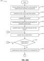
- FIGS. 10A-10F a flowchart 1000 illustrating a method for data transfer on the SoC 102, in accordance with an embodiment of the present invention, is shown.
- the CSI receiver 108 receives the sensor data and the first clock signal from the external camera sensor 104, i.e ., the first DPHY 202 receives the sensor data and the first clock signal.
- the first DPHY 202 generates the active, valid, and sync signals based on the sensor data.
- the first CSI controller 204 generates the data packet based on the sensor data received from the first DPHY 202.
- the first CSI controller 204 performs error correction on the data packet to generate the error signal.
- the first CSI controller 204 separates the packet header and the payload of the data packet and steps 1012 and 1014 are executed.
- the system memory write interface 208 writes the payload into the primary system memory 114.
- the first pipeline controller 212 decodes the type of the data packet based on the packet header.
- the first pipeline controller 212 receives the data packet from the error handler 210.
- the first pipeline controller 212 determines if the data packet is a long packet. If at step 1016, the first pipeline controller 212 determines that the data packet is a long packet, step 1018 is executed.
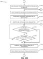
- the packet header of the data packet is communicated by the CSI receiver 108 to the CSI transmitter 112 over the command FIFO read interface.
- the first pipeline controller 212 writes the packet header of the long data packet into the first buffer 214.
- the first buffer 214 communicates the packet header of the long packet to the header read controller 310 of the CSI transmitter 112.
- the data formatter 216 packs the payload received from the error handler 210 to generate the formatted payload, and steps 1022 and 1024 are executed.
- the data formatter 216 writes the formatted payload into the second buffer 218.
- the formatted payload is written into the loopback buffer 110 by the second buffer 218 and step 1026 is executed.
- the header read controller 310 of the CSI transmitter 112 reads the packet header of the data packet from the first buffer 214.
- the header read controller 310 identifies the size of the payload from the packet header and step 1032 is executed.
- the data formatter 216 determines if the data packet is complete. If at step 1024, the data formatter 216 determines that the data packet is complete, step 1030 is executed. At step 1030, the CSI receiver 108 communicates the EOP signal to the CSI transmitter 112 and step 1032 is executed. However, if at step 1024, the data formatter 216 determines that the data packet is incomplete, step 1020 is executed.
- the CSI transmitter 112 determines if the payload is received completely by the loopback buffer 110. If at step 1032, the CSI transmitter 112 determines that the payload is not received completely by the loopback buffer 110, step 1034 is executed.
- the CSI transmitter 112 determines if the loopback buffer 110 is filled up to the threshold capacity. If at step 1034, the CSI transmitter 112 determines that the loopback buffer 110 is not filled up to the threshold capacity, step 1032 is executed. However, if at step 1034, the loopback buffer 110 determines that the loopback buffer 110 is filled up to the threshold capacity, step 1036 is executed. If at step 1032, the CSI transmitter 112 determines that the payload is received completely by the loopback buffer 110, step 1036 is executed.
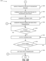
- the second pipeline controller 312 of the CSI transmitter 112 generates a read control signal.
- the second pipeline controller 312 receives the packet header of the data packet from the header read controller 310.
- the second pipeline controller 312 identifies the format of the payload and generates the read control signal.
- the data read controller 314 reads the formatted payload from the loopback buffer 110.
- the data read controller 314 further provides the formatted payload to the data un-formatter 316.
- the data un-formatter 316 unpacks the formatted payload to regenerate the payload.
- the data formatter 216 provides the regenerated payload to the second CSI controller 304.
- the second CSI controller 304 combines the packet header and the payload to regenerate the data packet.
- the second CSI controller 304 generates the loopback data based on the data packet and step 1046 is performed.
- the second CSI controller 304 generates the request signal for high speed transmission of the loopback data and step 1050 is executed.
- the second CSI controller 304 provides the request signal to the second DPHY 308 for requesting high speed transmission of the loopback data.
- step 1016 if the first pipeline controller 212 determines that the data packet is not a long packet, i.e., the data packet is a short packet, step 1048 is executed.
- step 1048 the first buffer 214 communicates the packet header of the data packet to the header read controller 310 and step 1046 is executed.
- the first buffer 214 receives the packet header of the data packet from the first pipeline controller 212.
- the second CSI controller 304 determines if the ready signal is generated by the second DPHY 308.
- the second DPHY 308 generates the ready signal in response to the request signal. If at step 1050, the second CSI controller 304 determines that the ready signal is generated by the second DPHY 308, step 1052 is executed. However, if at step 1050, the second CSI controller 304 determines that the ready signal is not generated by the second DPHY 308, the second CSI controller 304 waits for the generation of the ready signal.
- the CSI transmitter 112 outputs the loopback data.
- the second CSI controller 304 transmits the loopback data to the second DPHY 308 in response to the ready signal.
- the second DPHY 308 further transmits the loopback data to the processor 106.
- the CSI transmitter 112 determines if it has received the EOP signal from the CSI receiver 108. If at step 1054, the CSI transmitter 112 determines that it has received the EOP signal from the CSI receiver 108, step 1056 is executed. However, if at step 1054, the CSI transmitter 112 determines that it has not received the EOP signal from the CSI receiver 108, step 1052 is executed.
- the second CSI controller 304 exits the high-speed transmission of the loopback data.
- aforementioned method for data transfer on the SoC 102 may be performed for multiple data packets generated by the CSI receiver 108 based on the received sensor data in real-time.
- the multiple data packets are regenerated by the CSI transmitter 112 in real-time.
- the system 100 enables the transfer of the payload in real-time by way of the loopback buffer 110 from the CSI receiver 108 to the CSI transmitter 112.
- the primary system memory 114 is not used for the data transfer between the CSI receiver 108 and the CSI transmitter 112.
- the need to convert the loopback data to a format of the sensor data is eliminated.
- delays in the system 100 are reduced as there is no need to convert the format of the loopback data.
- the system 100 further compensates for frequency offset of the ppm differences between the first and second clock frequencies by transmitting the payload from the CSI receiver 108 to the CSI transmitter 112 through the loopback buffer 110.
- a system and method for real-time data transfer on a system-on-chip allows MIPI-CSI (camera serial interface) data received on a first interface to be output on another MIPI-CSI interface without using system memory or delaying the loopback path.
- the system includes a CSI receiver, a loopback buffer, and a CSI transmitter.
- the loopback buffer is used for the data transfer between the CSI receiver and the CSI transmitter.
- the CSI transmitter receives a payload included in a data packet from the CSI receiver by way of the loopback buffer.
- the CSI receiver communicates a packet header of the data packet to the CSI transmitter.
- the CSI transmitter reads the payload from the loopback buffer based on the packet header and at least one of a buffer threshold capacity and payload size.
Description
- The present invention relates generally to system-on-chips (SoCs) with high-speed serial interfaces, and, more particularly, to a system for transferring data between two high speed serial interfaces on a SoC.
- Many SoCs have two or more high-speed serial interfaces (HSSIs), and in certain scenarios, it is desirable to transfer data from the pads of one HSSI directly to the other HSSI. However, some standards, such as MIPI-CSI2 (Mobile Industry Processor Interface - Camera Serial Interface) standards do not allow pad to pad or traditional high-speed serial loopback methods. For such systems, if the received MIPI-CSI2 data is to be continuously monitored, the loopback path must have data tapped at locations different from the pad. Typically, to loopback the data, the data is tapped at the system memory, where it is stored for processing purposes. However, this requires a lot of system memory space and causes latencies due to additional system memory reads being performed to loopback the data.
- For operations such as testing the SoC, data output from a DSI (Digital Serial Interface) is compared with data provided to a CSI. However, as the DSI output data is in DSI format and the CSI data is in CSI format, the DSI format data must be converted to the CSI format for comparison, which causes additional processing delay.
Accordingly, it would be advantageous to have a system capable of transferring or looping back data between two or more HSSIs in real-time that does not require system memory and does not introduce long delays. - Abdennadher & Shaikh, in "Practices in High-Speed IO Testing", 2016 21st IEEE European Test Symposium (ETS), disclose a loopback BIST implementation in a typical PCIe interface.
-
US 2017/0201746 A1 discloses a system on chip including a display serial interface host device, a camera serial interface host device, a first register and a loopback control circuit, the first register configured to store a first flag indicating whether the system on chip is operating in a loopback mode or a non-loopback mode. - The MIPI Alliance Specification for M-PHY, Version 1.00.00, 8 February 2011, discloses a serial interface technology with high bandwidth capabilities, developed in particular for mobile applications.
-
US 2009/315899 A1 discloses a graphics multi-media integrated circuit connected to a host processor over two serial links: a half duplex bi-directional serial link which accords to a protocol defined for a display serial interface, and a uni-directional serial link which accords to a compatible protocol defined for a camera serial interface. - Aspects of the disclosure are defined in the accompanying claims. In a first aspect there is provided a system-on-chip (SoC) having two or more high-speed serial interfaces, the SoC comprising: a camera serial interface (CSI) receiver adapted to receive sensor data via a first serial interface and to generate a data packet that includes a payload; a loopback buffer connected to the CSI receiver, wherein the CSI receiver is adapted to write the payload into the loopback buffer; and a CSI transmitter connected between a second serial interface and the loopback buffer, characterized in that:
- the SoC is adapted to determine a threshold capacity of the loopback buffer based on the depth of the loopback buffer, said threshold capacity being a point to which the buffer may be filled without causing an overflow;
- the data packet generated by the CSI receiver further includes a packet header, the packet header including a data identifier, a word count and an error correction code, the word count specifying a size of the payload,
- wherein the CSI transmitter is configured to:
- receive the packet header from the CSI receiver;
- identify the size of the payload using the packet header;
- determine whether the size of the payload stored in the loopback buffer is equal to the size of the payload identified from the size information by comparing the identified size with an amount of the payload stored in the loopback buffer or is equal to the threshold capacity of the loopback buffer;
- read the payload from the loopback buffer when at least one of the threshold capacity of the loopback buffer is reached and the payload is received completely by the loopback buffer; and
- transmit the read payload over the second serial interface.
- In one or more embodiments, the CSI receiver may comprises: a first digital physical layer (DPHY) connected to an external camera sensor by way of the first interface for receiving the sensor data and a first clock signal, wherein the first DPHY outputs the sensor data, and generates active, sync, and valid signals, wherein the active signal is generated when the first DPHY is ready to transmit the sensor data, the sync signal is generated to synchronize a transmission frequency of the sensor data with a frequency of the first clock signal, and the valid signal is generated when the sensor data is valid; a first CSI controller connected to the first DPHY for receiving the sensor data and the active, sync, and valid signals, wherein the first CSI controller (i) generates the data packet, (ii) separates the payload and the packet header, (iii) outputs the payload and the packet header, (iv) performs error correction on the data packet to generate an error signal, and (v) generates an end of packet (EOP) signal, wherein the error signal indicates an error in the data packet and the EOP signal indicates an end of the data packet; and a first loopback controller connected to the first CSI controller for receiving the packet header, the payload, the EOP signal, and the error signal, wherein the first loopback controller (i) decodes a type of the data packet from the packet header, (ii) packs the payload to generate a formatted payload, and (iii) communicates the packet header and the EOP signal to the CSI transmitter, wherein the payload written by the CSI receiver into the loopback buffer is the formatted payload.
- In one or more embodiments, the first loopback controller may comprise: an error handler connected to the first CSI controller for receiving the packet header, the payload, the EOP signal, and the error signal, and outputting the packet header, the EOP signal, and the payload, wherein the error handler outputs the packet header and the payload when the error signal indicates that the data packet does not include an error; a first pipeline controller connected to the error handler for receiving the packet header and the EOP signal, wherein the first pipeline controller (i) decodes the type of the data packet from the packet header, (ii) outputs the packet header and the EOP signal, and (iii) generates a write control signal, wherein the first pipeline controller receives the EOP signal from the error handler when the error handler receives the complete payload; a first buffer connected to the first pipeline controller for receiving the packet header and the EOP signal, wherein the first buffer provides the packet header and the EOP signal to the CSI transmitter; a data formatter connected to the error handler and the first pipeline controller for receiving the payload and the write control signal, respectively, wherein the data formatter packs the payload based on the write control signal to generate the formatted payload when the type of the data packet is a long packet; and a second buffer connected to the data formatter for receiving the formatted payload, wherein the second buffer writes the formatted payload to the loopback buffer.
- In one or more embodiments, the CSI transmitter may comprise: a second loopback controller connected to the first loopback controller for reading the packet header, and receiving the EOP signal, wherein the second loopback controller also is connected to the loopback buffer for receiving the formatted payload, wherein the second loopback controller (i) unpacks the formatted payload to regenerate the payload and (ii) output the packet header; a second CSI controller connected to the second loopback controller for receiving the packet header and the payload, wherein the second CSI controller combines the packet header and the payload to regenerate the data packet and generates loopback data and a request signal for requesting high speed transmission of the loopback data, wherein a format of the loopback data is the same as a format of the sensor data; a second DPHY that receives a second clock signal, and is connected to the second CSI controller for receiving the request signal and the loopback data, wherein the second DPHY transmits a ready signal to the second CSI controller and the second CSI controller provides the loopback data to the second DPHY in response to the ready signal, and then the second DPHY outputs the loopback data over the second serial interface; and a phase locked loop (PLL) connected to the second DPHY for providing the second clock signal to the second DPHY, wherein a frequency of the second clock signal is equal to the frequency of the first clock signal.
- In one or more embodiments, the second loopback controller may comprise: a header read controller connected to the first buffer for reading the packet header and receiving the EOP signal, wherein the header read controller (i) identifies a size of the payload and (ii) outputs the packet header and payload size information; a second pipeline controller that receives a status signal, and is connected to the header read controller for receiving the packet header, wherein the second pipeline controller generates a read control signal; a data read controller connected to the header read controller, the second pipeline controller, and the loopback buffer for receiving the payload size information, the read control signal, and the formatted payload, respectively, and outputting the formatted payload, wherein the data read controller reads the formatted payload from the loopback buffer based on the size information and the read control signal; and a data un-formatter connected to the data read controller for receiving the formatted payload, wherein the data un-formatter (i) unpacks the formatted payload to regenerate the payload and (ii) generates the status signal, wherein the status signal indicates a status of unpacking the payload by the data un-formatter.
- In one or more embodiments, the SoC may further comprise a primary system memory connected to the CSI receiver, wherein the CSI receiver writes the payload into the primary system memory.
- In one or more embodiments, the CSI receiver may further comprise a system memory write interface connected to the first CSI controller for receiving the packet header, the payload, the EOP signal, and the error signal, wherein the CSI receiver writes the payload into the primary system memory.
- In a second aspect, there is provided a method for data transfer in a system-on-chip (SoC) that includes a camera serial interface (CSI) receiver connected to a first high-speed serial interface (HSSI), a loopback buffer, and a CSI transmitter connected to a second high-speed serial interface (HSSI), the method comprising:
- generating, by the CSI receiver, a data packet from data received over the first HSSI, wherein the data packet includes a payload and a packet header, the packet header including a data identifier, a word count and an error correction code, the word count specifying a size of the payload;
- writing, by the CSI receiver, the payload into the loopback buffer;
- determining a threshold capacity of the loopback buffer based on the depth of the loopback buffer, said threshold capacity being a point to which the buffer may be filled without causing an overflow;
- receiving, by the CSI transmitter, the packet header;
- identifying, by the CSI transmitter, the size of the payload using the packet header;
- determining by the CSI transmitter whether the size of the payload stored in the loopback buffer is equal to the size of the payload identified from the size information by comparing the identified size with an amount of the payload stored in the loopback buffer or is equal to the threshold capacity of the loopback buffer; and reading, by the CSI transmitter, the payload from the loopback buffer when at least one of the threshold capacity of the loopback buffer is reached and the payload is received completely by the loopback buffer, and transmitting the payload over the second HSSI.
- In one or more embodiments, the method may further comprise: receiving, by the CSI receiver, sensor data and a first clock signal from an external camera sensor over the first HSSI; generating, by the CSI receiver, valid and sync signals, wherein the sync signal is generated to synchronize a transmission frequency of the sensor data with a frequency of the first clock signal, and the valid signal is generated when the sensor data is valid; performing, by the CSI receiver, error correction on the data packet; separating, by the CSI receiver, the packet header and the payload of the data packet; writing, by the CSI receiver, the payload into the loopback buffer; and transmitting, by the CSI receiver, the packet header to the CSI transmitter.
- In one or more embodiments, the steps of writing the payload and transmitting the packet header may further comprise: decoding, by the CSI receiver, a type of the data packet from the packet header; packing, by the CSI receiver, the payload to generate a formatted payload when the type of the data packet is a long packet, wherein the payload written by the CSI receiver into the loopback buffer is the formatted payload; and communicating, by the CSI receiver, an end of packet (EOP) signal to the CSI transmitter, wherein the EOP signal indicates an end of the data packet.
- In one or more embodiments, the method may further comprise: reading, by the CSI transmitter, the formatted payload from the loopback buffer; regenerating, by the CSI transmitter, the payload; combining, by the CSI transmitter, the regenerated payload and the packet header to regenerate the data packet; generating, by the CSI transmitter, loopback data and a request signal for requesting high speed transmission of the loopback data, wherein the loopback data has the same format as the sensor data; generating, by the CSI transmitter, a ready signal in response to the request signal; and outputting the loopback data over the second HSSI by the CSI transmitter.
- In one or more embodiments, the step of regenerating the payload may further comprise: identifying, by the CSI transmitter, a size of the payload; generating, by the CSI transmitter, a read control signal; reading, by the CSI transmitter, the formatted payload from the loopback buffer based on the size of the payload and the read control signal; and unpacking, by the CSI transmitter, the formatted payload to regenerate the payload.
- In one or more embodiments, the method may further comprise writing, by the CSI receiver, the payload into a primary system memory of the SoC.
- The following detailed description of the preferred embodiments of the present invention will be better understood when read in conjunction with the appended drawings.
-
FIG. 1 is a block diagram of a system for data transfer in accordance with an embodiment of the present invention; -
FIG. 2 is a block diagram of an embodiment of a camera serial interface (CSI) receiver of the system ofFIG. 1 ; -
FIG. 3 is a block diagram of an embodiment of a CSI transmitter of the system ofFIG. 1 ; -
FIG. 4 is a timing diagram illustrating an operation of a first DPHY of the CSI receiver ofFIG. 2 in accordance with an embodiment of the present invention; -
FIG. 5 is a timing diagram illustrating an operation of a first CSI controller of the CSI receiver ofFIG. 2 in accordance with an embodiment of the present invention; -
FIG. 6 is a timing diagram illustrating an operation of a second CSI controller of the CSI transmitter ofFIG. 3 in accordance with an embodiment of the present invention; -
FIG. 7 is a timing diagram illustrating an operation of a second DPHY of the CSI transmitter ofFIG. 3 in accordance with an embodiment of the present invention; -
FIG. 8 is a timing diagram illustrating an operation of the CSI transmitter ofFIG. 1 in accordance with an embodiment of the present invention; -
FIG. 9 is a timing diagram illustrating an operation of a SoC ofFIG. 1 in accordance with an embodiment of the present invention; and -
FIGS. 10A-10F are a flow chart illustrating a method for data transfer on the SoC ofFIG. 1 , in accordance with an embodiment of the present invention. - The detailed description of the appended drawings is intended as a description of the currently preferred embodiments of the present invention, and is not intended to represent the only form in which the present invention may be practiced. It is to be understood that the same functions may be accomplished by different embodiments that are intended to be encompassed within the scope of the present invention, which is defined by the appended claims.
- Disclosed herein is a system-on-chip (SoC) including a camera serial interface (CSI) receiver, a loopback buffer, and a CSI transmitter. The CSI receiver receives sensor data and generates a data packet that includes a payload. The loopback buffer is connected to the CSI receiver. The CSI receiver writes the payload into the loopback buffer. The CSI transmitter is connected to the loopback buffer for reading the payload. The CSI transmitter reads the payload when at least one of a threshold capacity of the loopback buffer is reached and the payload is received completely by the loopback buffer.
- Also disclosed herein is a method for data transfer in a system-on-chip (SoC), where the SoC includes a CSI receiver, a loopback buffer, and a CSI transmitter. The method includes generating a data packet that includes a payload and writing the payload to the loopback buffer. The method further includes reading the payload from the loopback buffer when at least one of a threshold capacity of the loopback buffer is reached and the payload is received completely by the loopback buffer.
- Also disclosed herein is a system-on-chip (SoC) that includes a CSI receiver, a loopback buffer, and a CSI transmitter. The CSI receiver receives sensor data and generates a data packet that includes a payload. The loopback buffer is connected to the CSI receiver. The CSI receiver writes the payload into the loopback buffer. The CSI transmitter is connected to the loopback buffer for reading the payload. The CSI transmitter generates loopback data and reads the payload when at least one of a threshold capacity of the loopback buffer is reached and the payload is received completely by the loopback buffer. A format of the loopback data is the same as a format of the sensor data.
- Various embodiments of the present invention provide a method and system for transferring data between two high-speed serial interfaces (HSSI) in a SoC without using system memory. The SoC includes a CSI receiver connected to one HSSI, a loopback buffer, and a CSI transmitter connected to another HSSI. The CSI receiver receives raw sensor data from the first HSSI and generates a data packet including a header and a payload. The CSI receiver then writes the payload of the data packet into the loopback buffer. The CSI transmitter reads the payload from the loopback buffer when at least one of the threshold capacity is reached and the payload is received completely by the loopback buffer. The CSI transmitter also generates loopback data based on the amount of payload data read by the CSI transmitter. The sensor data and the loopback data both have the same format.
- The method and system eliminate the need to use system memory for data transfers between two HSSI. Further, as the loopback data and the sensor data have the same format, there is no need to convert the format of the loopback data to the format of the sensor data.
- Referring now to
FIG. 1 , a block diagram of a system for data transfer 100 (hereinafter referred to as "system 100"), in accordance with an embodiment of the present invention is shown. Thesystem 100 may be implemented in integrated circuits like SoCs and used for automotive applications such as a connected car, consumer applications such as a home security system, or industrial applications such as an industrial robotics. Thesystem 100 includes a system-on-chip (SoC) 102 connected to anexternal camera sensor 104 and aprocessor 106. In one embodiment, thesystem 100 acts as a measurement interface, and in another embodiment, thesystem 100 acts as a repeater interface. Although theprocessor 106 is shown as being external to theSoC 102, in other embodiments, theprocessor 106 is included in theSoC 102. - The
external camera sensor 104 captures an image or a video and outputs raw sensor data in a camera serial interface (CSI) format. Theexternal camera sensor 104 further outputs a first clock signal at a first frequency for synchronizing the transmission frequency of the sensor data with the first frequency. - The sensor data is received by the
SOC 102 in real-time via a first high-speed serial interface (HSSI). The sensor data is processed by theSoC 102 to generate loopback data, which is in the same format as that of the sensor data (i.e., in the CSI format). TheSoC 102 generates a second clock signal at a second frequency for synchronizing the transmission frequency of the loopback data with the second frequency. In a preferred embodiment, the second frequency is equal to the first frequency. The loopback data is then output at the second frequency over a second HSSI by theSoC 102. The signals and data that are received and generated by theSoC 102 are further shown in the timing diagram ofFIG. 9 . - The
SoC 102 includes aCSI receiver 108, aloopback buffer 110, aCSI transmitter 112, and aprimary system memory 114. In one embodiment, theCSI receiver 108 is a CSI-2 interface defined by the Mobile Industry Processor Interface (MIPI) protocol. The CSI-2 interface supports low power (LP) and high speed (HS) signaling modes. TheCSI receiver 108 is connected to theexternal camera sensor 104 via the first HSSI (i.e., MIPI-CSI2) to receive the sensor data and the first clock signal. TheCSI receiver 108 generates a data packet from the sensor data. The data packet may be a short or long packet type. - The data packet includes a packet header, a payload and, for a long type packet, a packet footer. The packet header includes a data identifier (ID), a word count (WC), and an error correction code (ECC). The WC specifies a size of the payload. The ID includes a virtual channel identifier (VC) and a data type (DT) value. The VC specifies a virtual channel over which the sensor data is received. The DT value specifies a format of the payload and the type of the data packet. The packet footer includes a checksum of the payload, which is used for correcting cyclic redundancy check (CRC) errors. The
CSI receiver 108 separates the packet header and the payload and outputs the packet header and the payload. When the data packet is a short packet, the data packet includes the packet header. - In a presently preferred embodiment, the
loopback buffer 110 is a dual-port first-in first-out (FIFO) memory. Theloopback buffer 110 is connected to theCSI receiver 108 to receive the payload by way of a write interface and buffers or stores the payload for a short period of time. - A depth of the
loopback buffer 110 is based on various delays in thesystem 100 such as the time required to write the payload into theloopback buffer 110 and the time required to read the payload from theloopback buffer 110. The depth of theloopback buffer 110 also is based on a delay in handling HS signaling and delays in clock uncertainties of theCSI receiver 108 and theCSI transmitter 112. A threshold capacity of theloopback buffer 110 is based on the depth of theloopback buffer 110. The threshold capacity is the point to which the buffer may be filled without causing an overflow. In the presently preferred embodiment, thebuffer 110 has a threshold capacity such that an overflow of the payload is avoided while theloopback buffer 110 is receiving the payload. - The
CSI transmitter 112 is connected to theCSI receiver 108 by way of a command FIFO read interface, which allows thetransmitter 112 to read the packet header from thereceiver 108. TheCSI transmitter 112 also is connected to theloopback buffer 110 by way of a read interface. - The
CSI transmitter 112 identifies the size of the payload using the packet header. Based on the identified size, theCSI transmitter 112 determines whether the size of the payload is equal to the buffer threshold capacity by comparing the identified size with an amount of the payload stored in theloopback buffer 110. To determine the amount of the payload stored in theloopback buffer 110, theCSI transmitter 112 checks addresses that are pointed to by a read pointer and a write pointer of theloopback buffer 110. The addresses pointed to are used to determine the amount of the payload stored in theloopback buffer 110. TheCSI transmitter 112 reads the payload from theloopback buffer 110 when at least one of the size of the payload equals the threshold capacity (i.e., if the threshold capacity of theloopback buffer 110 is reached) and the size of the payload equals the amount of the payload stored in the loopback buffer 110 (i.e., if theloopback buffer 110 has received the entire payload). - The
CSI transmitter 112 regenerates the data packet by combining the packet header and the payload. TheCSI transmitter 112 then generates the loopback data and the second clock signal based on the data packet. The loopback data is transmitted at the second clock frequency to components (such as the processor 106) by way of the second HSSI. Thus, using thereceiver 108,buffer 110 andtransmitter 112, theSoC 102 is able to receive data from one HSSI and output the data over a second HSSI without using thesystem memory 114. - The
primary system memory 114 is a main memory of theSoC 102. Theprimary system memory 114 is connected to theCSI receiver 108 to receive the payload. The payload is thus stored in thesystem memory 114 and may be used when a display operation to display video or image data is performed. In accordance with the present invention, thesystem 100 does not use thesystem memory 114 to transfer data between either theCSI receiver 108 and theCSI transmitter 112, or the first and second HSSIs. - The
processor 106 is connected to theSoC 102 to receive the loopback data and the second clock signal. In one embodiment, theprocessor 106 is used to test theSoC 102 by comparing the sensor data and the loopback data to determine whether the sensor data matches the loopback data. If the loopback data does not match the sensor data, theprocessor 106 indicates that theSoC 102 may have a fault. If the loopback data matches the sensor data, theprocessor 106 determines that theSoC 102 is functioning correctly. - Referring now to
FIG. 2 , a block diagram of theCSI receiver 108, in accordance with an embodiment of the present invention, is shown. TheCSI receiver 108 includes a first digital physical layer (DPHY) 202, afirst CSI controller 204, afirst loopback controller 206, and a systemmemory write interface 208. - The
first DPHY 202 is connected to the first HSSI and operates in accordance with the MIPI protocol. Thefirst DPHY 202 may include multiple DPHY masters or multiple DPHY slaves that enable thefirst DPHY 202 to operate in a master or slave mode. In one embodiment of the present invention, thefirst DPHY 202 operates in the slave mode. - The
first DPHY 202 is connected to theexternal camera sensor 104 for receiving the first clock signal by way of a first clock lane of an interface. The first clock lane includes positive and negative clock lines. Thefirst DPHY 202 further receives the sensor data from theexternal camera sensor 104 by way of multiple data lanes. Each data lane includes a positive data line (DP) and a negative data line (DN). During HS signaling mode, each data lane carries a corresponding part of the sensor data at a high data rate (such as 2.5 gigabit per second (Gbps)) and is driven by a low-swing differential signal. In the LP signaling mode, each data lane carries signals at a low data rate (such as 10 megabits per second (Mbps)). It will be understood by those of skill in the art that a data lane that has a positive line and a negative line means refers to a differential signal. - The
first DPHY 202 generates an active signal when it is ready for transmission of the sensor data, and a sync signal to synchronize the sensor data transmission frequency with the first frequency. Thefirst DPHY 202 further determines whether the sensor data is valid, i.e., thefirst DPHY 202 determines whether the received sensor data is in the CSI format. On determining that the sensor data is valid, thefirst DPHY 202 generates a valid signal (e.g., at a logic high state). In one embodiment, if the sensor data received by thefirst DPHY 202 is invalid, thefirst DPHY 202 generates the valid signal at logic low state and transmits the low valid signal to thefirst CSI controller 204. - The
first CSI controller 204 is connected to thefirst DPHY 202 to receive the sensor data in a byte format by way of multiple data lanes of a first PHY protocol interface (PPI). Thefirst CSI controller 204 further receives active, sync, and valid signals from thefirst DPHY 202. Thefirst CSI controller 204 unpacks each byte of the sensor data into pixels to generate the data packet. - To determine whether the data packet includes any errors, the
first CSI controller 204 performs error correction on the data packet and generates an error signal. In one embodiment, thefirst CSI controller 204 detects errors (such as an ECC error, CRC error, or a high-speed exit error) in the data packet and activates the error signal. If the data packet is error free, then theCSI controller 204 does not activate the error signal. Thefirst CSI controller 204 further generates a header valid signal that indicates whether the packet header is valid (i.e., the packet header is error-free). Similarly, thefirst CSI controller 204 generates a data valid signal when it determines that the payload is valid (i.e., the payload is error-free). Thefirst CSI controller 204 generates an SOP signal and an EOP signal, which indicate a start of the data packet and an end of the data packet, respectively. The error signal, the header valid signal, the data valid signal, the SOP signal, and the EOP signal are control signals generated by thefirst CSI controller 204. Thefirst CSI controller 204 separates and outputs the packet header and the payload of the data packet. - The
first loopback controller 206 is connected to thefirst CSI controller 204 to receive the packet header, the payload, and the control signals. In a presently preferred embodiment, thefirst loopback controller 206 includes anerror handler 210, afirst pipeline controller 212, afirst buffer 214, adata formatter 216, and asecond buffer 218. - The
error handler 210 is connected to thefirst CSI controller 204 to receive the packet header, the payload, and the control signals. Theerror handler 210 receives the data packet based on the SOP signal. The error signal, the header valid signal, and the data valid signal are used to indicate an erroneous data packet, an invalid header, and an invalid payload, respectively, in which case theerror handler 210 discards the data packet. Theerror handler 210 may further generate default data based on the data packet to maintain continuity of data flow. If no error is indicated, then theerror handler 210 outputs the packet header, the payload, and the EOP signal. - The
first pipeline controller 212 is connected to theerror handler 210 to receive the packet header and the EOP signal. Based on the packet header, thefirst pipeline controller 212 decodes the data packet type, such a long or short packet. Thefirst pipeline controller 212 identifies a format of the payload from the packet header. For a long packet type and based on the identified format, thefirst pipeline controller 212 will generate a write control signal. - The
first buffer 214 is connected to thefirst pipeline controller 212, which writes the packet header and the EOP signal to thefirst buffer 214. In the presently preferred embodiment, thefirst buffer 214 is a FIFO memory that buffers (i.e., stores) the packet header for a short period of time. TheCSI transmitter 112 reads the packet header and the EOP signal from thefirst buffer 214. - The data formatter 216 is connected to the
error handler 210 to receive the payload. The data formatter 216 also is connected to thefirst pipeline controller 212 to receive the write control signal. If thefirst pipeline controller 212 identifies the packet as a long type packet, then thefirst pipeline controller 212 writes the packet header into thefirst buffer 214 and transmits the write control signal to thedata formatter 216. - The data formatter 216 includes a FIFO buffer (not shown) that temporarily stores the payload data. The data formatter 216 further receives the write control signal, which indicates an amount of the payload to be packed by the
data formatter 216. The amount of the payload to be packed is based on the format of the payload. For example, if the payload is RGB format, then the amount of the payload to be packed is 1 byte. In another example, if the payload is a RAW format, then the amount of the payload to be packed is 3 bytes. The data formatter 216 thus packs (i.e., compresses) the payload to generate a formatted payload. - The
second buffer 218 preferably comprises a FIFO memory that is used to buffer the formatted payload data. Thesecond buffer 218 is connected to the data formatter 216 to receive the formatted payload data. Thesecond buffer 218 writes the formatted payload data into theloopback buffer 110. - The system
memory write interface 208 is connected to thefirst CSI controller 204 to receive the packet header, the payload, and the control signals. The systemmemory write interface 208 writes the payload into theprimary system memory 114, based on the error signal. If the error signal indicates that there is an error in the data packet, then the systemmemory write interface 208 may discard the payload. If the error signal indicates that the data packet is error-free, then the systemmemory write interface 208 writes the payload into theprimary system memory 114. - Referring now to
FIG. 3 , a block diagram of theCSI transmitter 112, in accordance with an embodiment of the present invention, is shown. TheCSI transmitter 112 includes asecond loopback controller 302, asecond CSI controller 304, a phase locked loop (PLL) 306, and asecond DPHY 308. - The
second loopback controller 302 is connected to theloopback buffer 110 to receive the formatted payload data. Thesecond loopback controller 302 also is connected to thefirst loopback controller 206 for reading the packet header. Thefirst loopback controller 206 further communicates the EOP signal to thesecond loopback controller 302. Thesecond loopback controller 302 includes a header readcontroller 310, asecond pipeline controller 312, a data readcontroller 314, and adata un-formatter 316. - The header read
controller 310 is connected to thefirst buffer 214 to read the packet header and receive the EOP signal. Based on the packet header, the header readcontroller 310 identifies the size of the payload. The header readcontroller 310 outputs the packet header and payload size information. - The
second pipeline controller 312 is connected to the header readcontroller 310 to receive the packet header. Thesecond pipeline controller 312 identifies the format of the payload from the packet header and generates a read control signal. The read control signal indicates an amount of the formatted payload to be read by the data readcontroller 314. For example, if the payload is in RGB format, then the amount of the formatted payload to be read is 1 byte. In another example, if the payload is in RAW format, then the amount of the formatted payload to be read is 3 bytes. - The data read
controller 314 is connected to the header readcontroller 310 and thesecond pipeline controller 312 to receive the size information and the read control signal, respectively. The data readcontroller 314 also is connected to theloopback buffer 110 to read the formatted payload based on the size information and the read control signal. The data readcontroller 314 reads the formatted payload from theloopback buffer 110 when the data readcontroller 314 determines that the size of the formatted payload stored in theloopback buffer 110 equals the size of the payload identified from the size information or equals the threshold capacity of theloopback buffer 110. - The data un-formatter 316 is connected to the data read
controller 314 to receive the formatted payload data. The data un-formatter 316 includes a second FIFO memory (not shown) for buffering the formatted payload data. The data un-formatter 316 unpacks, i.e., decompresses the formatted payload data to regenerate the payload data. When the amount of the formatted payload data buffered by the second FIFO is less than a threshold capacity of the second FIFO, the data un-formatter 316 generates a status signal. - The
second pipeline controller 312 also is connected to the data un-formatter 316 to receive the status signal. Based on the value of the status signal, thesecond pipeline controller 312 generates the read control signal for the data readcontroller 314 to avoid an underflow of the formatted payload in the second FIFO. - The
second CSI controller 304 is connected to the data un-formatter 316 and thesecond pipeline controller 312 to receive the payload and the packet header, respectively. Thesecond CSI controller 304 combines the packet header and the payload to re-generate the data packet. Thesecond CSI controller 304 also packs (i.e., converts) the payload data of the regenerated data packet (which is in a pixel format to a byte format) to generate the loopback data. - The transmission of the packet header and the payload between the
second loopback controller 302 and thesecond CSI controller 304 is based on data signals such as a command request signal, a command acknowledgement signal, a read signal, and a read enable signal. The packet header of a short packet may include a command such as a frame start command or a frame end command. The frame start command indicates a start of an image frame of a video that includes multiple data packets. The frame end command indicates an end of the image frame of the video. - The
second pipeline controller 312 generates the command request signal to request transmission of the command and provides the command request signal to thesecond CSI controller 304. In response to the command request signal, thesecond CSI controller 304 generates a command acknowledgement signal, which indicates that thesecond CSI controller 304 is ready to receive the command. Thesecond pipeline controller 312 also generates read enable and read enable last signals. The read enable signal indicates transmission of the payload by thesecond loopback controller 302 to thesecond CSI controller 304 and the read enable last signal indicates transmission of a last byte of the payload by thesecond loopback controller 302 to thesecond pipeline controller 312. - The
second DPHY 308 is connected to the second HSSI and operates according to the MIPI protocol. Thesecond DPHY 308 may include multiple DPHY masters or multiple DPHY slaves that enable thefirst DPHY 202 to operate in a master or slave mode. In one embodiment, thefirst DPHY 202 operates in the master mode. - The
second DPHY 308 is connected to thePLL 306 and thesecond CSI controller 304 to receive the second clock signal and the request signal, respectively. Thesecond CSI controller 304 generates the request signal for requesting high speed transmission of the loopback data. Thesecond CSI controller 304 provides the request signal to the first DPHY over a second PPI. In response to the request signal, thesecond DPHY 308 generates a ready signal and transmits the ready signal to thesecond CSI controller 304 when thesecond DPHY 308 is ready for high speed transmission of the loopback. In response to the ready signal, thesecond CSI controller 304 transmits the loopback data to thesecond DPHY 308 over the second PPI. Thesecond DPHY 308 thus receives the loopback data and transmits the loopback data at a high speed. - The
second DPHY 308 transmits the second clock signal and the loopback data over a second clock lane and multiple data lanes to theprocessor 106, respectively. The second clock lane includes positive and negative clock lines. Further, each data lane includes positive and negative data lines (i.e., for differential signaling). - Referring now to
FIG. 4 , a timing diagram 400 illustrating an operation of thefirst DPHY 202, in accordance with an embodiment of the present invention is shown. From time T0-T2, the active, valid, and sync signals are at logic low state. - From time T2-T3, the
first DPHY 202 generates the active signal (e.g., at logic high state) when thefirst DPHY 202 is ready for transmission of the sensor data. Thefirst DPHY 202 also generates the sync signal (e.g., at logic high state) for synchronizing the frequency of transmission of the sensor data with the first frequency. The valid signal remains low. - From time T3-T4, the sync signal transitions from high to low. The active signal remains high and the
first DPHY 202 initiates the transmission of the sensor data to thefirst CSI controller 204. Thefirst DPHY 202 generates the valid signal (e.g., at logic high state). Thefirst CSI controller 204 receives a first data byte 'B1' of the sensor data from thefirst DPHY 202. - From time T4-T12, the active signal and the valid signal remain high. Thus, the
first DPHY 202 transmits the remaining data bytes 'B2-C' of the sensor data to thefirst CSI controller 204. - From time T12-T13, the active and valid signals transition from high to low.
- From time T13-T16, the active, valid, and sync signals continue to remain low.
- Referring now to
FIG. 5 , a timing diagram 500 illustrating an operation of thefirst CSI controller 204, in accordance with an embodiment of the present invention, is shown. - From time T0-T2, the header valid signal is at logic low state. The SOP, EOP, and data valid signals also are at logic low state. Further, a number of pixels in the payload are specified by a pixel count. From time T2-T3, the header valid signal transitions from low to high. The
first CSI controller 204 transmits the packet header to thefirst loopback controller 206. Thefirst CSI controller 204 further communicates the DT, WC, and VC corresponding to the data packet. For example, the DT may be 02, the WC may be 08, and the VC may be 0. - From time T3-T4, the header valid signal transitions from high to low. The SOP, EOP, and data valid signals remain low. Further, the
error handler 210 receives the DT, WC, and VC. - From time T4-T16, the header valid, SOP, EOP, and data valid signals remain low.
- Referring now to
FIG. 6 , a timing diagram 600 illustrating an operation of thesecond CSI controller 304, in accordance with an embodiment of the present invention, is shown. - From time T0-T1, the command request and command acknowledgement signals are at logic low state. The read enable and read enable last signals also are at logic low state.
- From time T1-T2, the
second CSI controller 304 receives the command request signal, which is at logic high state, and the transmission of the command by thesecond pipeline controller 312 to thesecond CSI controller 304 is initiated. - From time T2-T3, the command acknowledgement signal transitions from low to high. Thus, the
second CSI controller 304 receives the command 2a000a. - From time T3-T4, the command request and command acknowledgement signals transition from high to low.
- From time T4-T5, the read enable signal transitions from low to high.
- From time T5-T6, the
second CSI controller 304 receives a first even byte, such as 00, and a first odd byte, such as 01, of the payload. The read enable signal transitions from high to low. - From time T6-T7, the read enable signal transitions from low to high.
- From time T7-T9, the read enable signal remains at logic high state. The
second CSI controller 304 receives second and third even bytes, such as 02 and 04, and second and third odd bytes, such as 03 and 05, of the payload. - From time T9-T10, the read enable signal remains at logic high state and the read enable last signal transitions from low to high. The
second CSI controller 304 receives a fourth even byte, such as 06, and a fourth odd byte, such as 07, of the payload. - From time T10-T11, the
second CSI controller 304 receives a last even byte of the payload such as 08, and a last odd byte, such as 09, of the payload. The read enable and read enable last signals transition from high to low. - From time T11-T16, the command request, command acknowledgement, read enable, and read enable last signals remain low.
- Referring now to
FIG. 7 , a timing diagram 700 illustrating an operation of thesecond DPHY 308, in accordance with an embodiment of the present invention, is shown. - From time T0-T2, the request and ready signals are at logic low state.
- From time T2-T3, the
second CSI controller 304 generates the request signal (e.g., at logic high state) for high speed transmission of the loopback data. Thesecond DPHY 308 receives the request signal and thesecond CSI controller 304 initiates transmission of a first data byte 'B1' to thesecond DPHY 308. - From time T3-T4, the request signal remains high and the ready signal remains low. The time period T3-T5, i.e., start-up time, is a time duration between the reception of the request signal and generation of the ready signal by the
second CSI controller 304. - From time T4-T5, the
second DPHY 308 generates the ready signal in response to the request signal. Thesecond DPHY 308 receives the first data byte 'B1' of the loopback data from thesecond CSI controller 304. - From time T5-T12, the request signal and the ready signal remain high. Thus, the
second DPHY 308 receives the remaining data bytes 'B2-Bn' of the loopback data from thesecond CSI controller 304. - From time T12-T13, the request signal transitions from high to low and the ready signal remains at high.
- From time T13-T14, the ready signal transitions from high to low as the request signal is low. The
second DPHY 308 exits the high-speed transmission state. - From time T14-T16, the request signal and the ready signal remain low. The time from T14-T16, i.e., shut-down time, is the time required by the
second CSI controller 304 to terminate the high-speed transmission state. - Referring now to
FIG. 8 , a timing diagram 800 illustrating an operation of theCSI transmitter 112, in accordance with an embodiment of the present invention, is shown. A start-of-transmission (SOT) sequence as defined in the MIPI protocol is performed before initiating high speed transmission of data. TheCSI transmitter 112 transitions from a stop state (LP-11) to a HS mode by way of the SOT sequence. - From time T0-T1, a first signal (DP0) transmitted over DP is at logic high state and a second signal (DN0) over DN is at logic high state. Thus, the
CSI transmitter 112 is in the stop state (LP-11) of the SOT sequence. - From time T1-T3, DP0 transitions from high to low and DN0 remains at high. Thus, the
CSI transmitter 112 is in a HS request state (LP-01) of the SOT sequence. - From time T3-T5, DN0 transitions from high to low, whereas DP0 remains low. Thus, the
CSI transmitter 112 is in a HS prepare state (LP-00) of the SOT sequence. The time period T2-T4, i.e., TLPX, is the time required for initiating the HS request state. - From time T5-T6, the
CSI transmitter 112 transitions from the LP mode to the HS mode. The time period T4-T6, i.e., THS-PREPARE, is the time required for initiating the HS prepare state. - From time T6-T8, the
CSI transmitter 112 enters the high-speed mode of data transmission. The time period T6-T8, i.e., THS-ZERO, is the time required for initiating the HS-0 state of the SOT sequence. The time period T4-T7, i.e., THS-SETTLE, is the time period during which an HS receiver (not shown) in theprocessor 106 ignores any transitions of DP0 and DN0. - From time T8-T11, the
CSI transmitter 112 transmits a synchronous code to synchronize the transmission frequency of high-speed data with the second frequency. The time period T8-T11, i.e., THS-SYNC, is the time required to transmit the synchronous code. - From time T41-T12, the
CSI transmitter 112 transmits a first data byte of the loopback data. Thus, theCSI transmitter 112 initiates transmission of the loopback data. - From time T12-T16, the
CSI transmitter 112 transmits the remaining data bytes of the loopback data. - From time T16-T18, the
CSI transmitter 112 drives a flipped last data byte of the loopback data immediately after transmitting the last byte of the loopback data. The time period T16-T18, i.e., THS-TRAIL, is the time for which theCSI transmitter 112 drives the flipped last data byte of the loopback data. - From time T18-T20, the
CSI transmitter 112 exits the HS mode and enters the stop state (LP-11). The time period T18-T20, i.e., THS-EXIT, is the time required for theCSI transmitter 112 to exit the HS mode. The time period T16-T19, i.e., THS-EOT, is the time required for theCSI transmitter 112 to initiate end-of-transmission sequence defined in the MIPI protocol. The time period T18-T19, i.e., TREOT, is 30%-85% rise time of DP0 or DN0 in the LP signaling mode. The time period T17-T19, i.e., THS-SKIP, is the time period during which the HS receiver ignores any transitions of DP0 and DN0. - The delay in handling HS signaling is based on at least one of the THS-TRAIL and the THS-EXIT, the start-up time, the shut-down time, and the time required to transition from the stop state to the HS request state. The delays in clock uncertainties of the
CSI receiver 108 and theCSI transmitter 112 are based on parts-per-million (ppm) differences in the frequencies of the first and second clock signals. A delay in the logic pipeline and synchronization of the loopback data occurs due to the time required by thesecond CSI controller 304 to provide the request signal to thesecond DPHY 308, the time period between reception of the command request signal and the payload by thesecond CSI controller 304, and a time required to synchronize the loopback data. The depth of theloopback buffer 110 is determined based on the delays in handling HS signaling, clock uncertainties, and logic pipeline and synchronization of the loopback data at different data rates such as 2.5 Gbps or 10 Mbps. - Referring now to
FIG. 9 , a timing diagram 900 illustrating an operation of theSoC 102, in accordance with an embodiment of the present invention, is shown. In this operation, theSoC 102 receives the first clock signal as first positive and negative clock signals (CLK1P and CLK1N) over the first clock lane. TheSoC 102 also receives the sensor data as first through third positive and negative input signals (D1P0-D1P2 and D1N0-D1N2) over first through third data lanes. TheSoC 102 transmits the second clock signal as the second positive and negative clock signals (CLK2P and CLK2N) of the second clock lane, and the loopback data as fourth through sixth positive and negative output signals (D2P0-D2P2 and D2N0-D2N2) over fourth through sixth data lanes. Based on the sensor data, theSoC 102 receives the D1P0-D1P2 and D1N0-D1N2 and transmits the D2P0-D2P2 and D2N0-D2N2. - At time T0, the D1P0-D1P2 and D1N0-D1N2 are at logic high state, and D2P0-D2P2 and D2N0-D2N2 are at logic high state.
- At time T1, D1P0-D1P2 transition from high to low, D1N0-D1N2 remain high, and D2P0-D2P2 and D2N0-D2N2 also remain high.
- At time T2, D1P0-D1P2 remain low, D1N0-D1N2 transition from high to low, and D2P0-D2P2 and D2N0-D2N2 remain high.
- At time T2, D1P0-D1P2 and D1N0-D1N2 remain low, D2P0-D2P2 transition from high to low, and D2N0-D2N2 remain high.
- At time T4, D1P0-D1P2 remain low, D1N0-D1N2 transition from low to high, D2P0-D2P2 remain low, and D2N0-D2N2 transition from high to low.
- At time T5, D1P0-D1P2 transition from low to high, D1N0-D1N2 remain high, and D2P0-D2P2 and D2N0-D2N2 remain low.
- At time T6, D1P0-D1P2 remain high, D1N0-D1N2 transition high to low, D2P0-D2P2 remain low, and D2N0-D2N2 transition from low to high.
- At time T7, D1P0-D1P2 remain high, D1N0-D1N2 remain low, D2P0-D2P2 transition from low to high, and D2N0-D2N2 remain high.
- At time T8, D1P0-D1P2 remain high, D1N0-D1N2 transition from low to high, D2P0-D2P2 remain high, and D2N0-D2N2 transition from high to low.
- At time Tg, D1P0-D1P2 transition from high to low, D1N0-D1N2 and D2P0-D2P2 remain high, and D2N0-D2N2 remain low.
- At time T10, D1P0-D1P2 remain low, D1N0-D1N2 and D2P0-D2P2 remain high, and D2N0-D2N2 transition from low to high.
- At time T11, D1P0-D1P2 remain low, D1N0-D1N2 remain high, D2P0-D2P2 remain high, and D2N0-D2N2 remain high.
- At time T12, D1P0-D1P2 remain low, D1N0-D1N2 transition from high to low, D2P0-D2P2 remain high, and D2N0-D2N2 remain high.
- At time T12, D1P0-D1P2 remain low, D1N0-D1N2 remain low, D2P0-D2P2 remain high, and D2N0-D2N2 remain high.
- At time T14, D1P0-D1P2 remain at low, D1N0-D1N2 transition from low to high, D2P0-D2P2 remain high, and D2N0-D2N2 remain at high.
- At time T15, D1P0-D1P2 remain low, D1N0-D1N2 remain high, D2P0-D2P2 transition from high to low, and D2N0-D2N2 remain high.
- At time T16, D1P0-D1P2 remain low, D1N0-D1N2 remain high, D2P0-D2P2 remain low, and D2N0-D2N2 transition from high to low.
- At time T17, D1P0-D1P2 remain at low, D1N0-D1N2 remain high, D2P0-D2P2 remain low. The D2N0-D2N2 remain low.
- At time T18, D1P0-D1P2 remain low, D1N0-D1N2 remain high, D2P0-D2P2 remain low, and D2N0-D2N2 transition from low to high.
- At time T19, D1P0-D1P2 remain low, D1N0-D1N2 remain high, D2P0-D2P2 remain low, and D2N0-D2N2 remain high.
- Referring now to
FIGS. 10A-10F , aflowchart 1000 illustrating a method for data transfer on theSoC 102, in accordance with an embodiment of the present invention, is shown. - At
step 1002, theCSI receiver 108 receives the sensor data and the first clock signal from theexternal camera sensor 104, i.e., thefirst DPHY 202 receives the sensor data and the first clock signal. Atstep 1004, thefirst DPHY 202 generates the active, valid, and sync signals based on the sensor data. - At
step 1006, thefirst CSI controller 204 generates the data packet based on the sensor data received from thefirst DPHY 202. Atstep 1008, thefirst CSI controller 204 performs error correction on the data packet to generate the error signal. - At
step 1010, thefirst CSI controller 204 separates the packet header and the payload of the data packet andsteps step 1012, the systemmemory write interface 208 writes the payload into theprimary system memory 114. Atstep 1014, thefirst pipeline controller 212 decodes the type of the data packet based on the packet header. Thefirst pipeline controller 212 receives the data packet from theerror handler 210. Atstep 1016, thefirst pipeline controller 212 determines if the data packet is a long packet. If atstep 1016, thefirst pipeline controller 212 determines that the data packet is a long packet,step 1018 is executed. - At
step 1018, the packet header of the data packet is communicated by theCSI receiver 108 to theCSI transmitter 112 over the command FIFO read interface. Thefirst pipeline controller 212 writes the packet header of the long data packet into thefirst buffer 214. Thefirst buffer 214 communicates the packet header of the long packet to the header readcontroller 310 of theCSI transmitter 112. Atstep 1020, the data formatter 216 packs the payload received from theerror handler 210 to generate the formatted payload, andsteps second buffer 218. - At
step 1022, the formatted payload is written into theloopback buffer 110 by thesecond buffer 218 andstep 1026 is executed. Atstep 1026, the header readcontroller 310 of theCSI transmitter 112 reads the packet header of the data packet from thefirst buffer 214. Atstep 1028, the header readcontroller 310 identifies the size of the payload from the packet header andstep 1032 is executed. - At
step 1024, the data formatter 216 determines if the data packet is complete. If atstep 1024, the data formatter 216 determines that the data packet is complete,step 1030 is executed. Atstep 1030, theCSI receiver 108 communicates the EOP signal to theCSI transmitter 112 andstep 1032 is executed. However, if atstep 1024, the data formatter 216 determines that the data packet is incomplete,step 1020 is executed. - At
step 1032, theCSI transmitter 112 determines if the payload is received completely by theloopback buffer 110. If atstep 1032, theCSI transmitter 112 determines that the payload is not received completely by theloopback buffer 110,step 1034 is executed. - At
step 1034, theCSI transmitter 112 determines if theloopback buffer 110 is filled up to the threshold capacity. If atstep 1034, theCSI transmitter 112 determines that theloopback buffer 110 is not filled up to the threshold capacity,step 1032 is executed. However, if atstep 1034, theloopback buffer 110 determines that theloopback buffer 110 is filled up to the threshold capacity,step 1036 is executed. If atstep 1032, theCSI transmitter 112 determines that the payload is received completely by theloopback buffer 110,step 1036 is executed. - At
step 1036, thesecond pipeline controller 312 of theCSI transmitter 112 generates a read control signal. Thesecond pipeline controller 312 receives the packet header of the data packet from the header readcontroller 310. Thesecond pipeline controller 312 identifies the format of the payload and generates the read control signal. - At
step 1038, the data readcontroller 314 reads the formatted payload from theloopback buffer 110. The data readcontroller 314 further provides the formatted payload to thedata un-formatter 316. Atstep 1040, the data un-formatter 316 unpacks the formatted payload to regenerate the payload. The data formatter 216 provides the regenerated payload to thesecond CSI controller 304. - At
step 1042, thesecond CSI controller 304 combines the packet header and the payload to regenerate the data packet. Atstep 1044, thesecond CSI controller 304 generates the loopback data based on the data packet andstep 1046 is performed. Atstep 1046, thesecond CSI controller 304 generates the request signal for high speed transmission of the loopback data andstep 1050 is executed. Thesecond CSI controller 304 provides the request signal to thesecond DPHY 308 for requesting high speed transmission of the loopback data. - At
step 1016, if thefirst pipeline controller 212 determines that the data packet is not a long packet, i.e., the data packet is a short packet,step 1048 is executed. Atstep 1048, thefirst buffer 214 communicates the packet header of the data packet to the header readcontroller 310 andstep 1046 is executed. Thefirst buffer 214 receives the packet header of the data packet from thefirst pipeline controller 212. - At
step 1050, thesecond CSI controller 304 determines if the ready signal is generated by thesecond DPHY 308. Thesecond DPHY 308 generates the ready signal in response to the request signal. If atstep 1050, thesecond CSI controller 304 determines that the ready signal is generated by thesecond DPHY 308,step 1052 is executed. However, if atstep 1050, thesecond CSI controller 304 determines that the ready signal is not generated by thesecond DPHY 308, thesecond CSI controller 304 waits for the generation of the ready signal. - At
step 1052, theCSI transmitter 112 outputs the loopback data. Thesecond CSI controller 304 transmits the loopback data to thesecond DPHY 308 in response to the ready signal. Thesecond DPHY 308 further transmits the loopback data to theprocessor 106. Atstep 1054, theCSI transmitter 112 determines if it has received the EOP signal from theCSI receiver 108. If atstep 1054, theCSI transmitter 112 determines that it has received the EOP signal from theCSI receiver 108,step 1056 is executed. However, if atstep 1054, theCSI transmitter 112 determines that it has not received the EOP signal from theCSI receiver 108,step 1052 is executed. Atstep 1056, thesecond CSI controller 304 exits the high-speed transmission of the loopback data. - It will be apparent to a person having ordinary skill in the art that aforementioned method for data transfer on the
SoC 102 may be performed for multiple data packets generated by theCSI receiver 108 based on the received sensor data in real-time. The multiple data packets are regenerated by theCSI transmitter 112 in real-time. - The
system 100 enables the transfer of the payload in real-time by way of theloopback buffer 110 from theCSI receiver 108 to theCSI transmitter 112. Thus, theprimary system memory 114 is not used for the data transfer between theCSI receiver 108 and theCSI transmitter 112. Further, as the sensor data and the loopback data are in the same format, the need to convert the loopback data to a format of the sensor data is eliminated. Additionally, delays in thesystem 100 are reduced as there is no need to convert the format of the loopback data. Thesystem 100 further compensates for frequency offset of the ppm differences between the first and second clock frequencies by transmitting the payload from theCSI receiver 108 to theCSI transmitter 112 through theloopback buffer 110. - A system and method for real-time data transfer on a system-on-chip (SoC) allows MIPI-CSI (camera serial interface) data received on a first interface to be output on another MIPI-CSI interface without using system memory or delaying the loopback path. The system includes a CSI receiver, a loopback buffer, and a CSI transmitter. The loopback buffer is used for the data transfer between the CSI receiver and the CSI transmitter. The CSI transmitter receives a payload included in a data packet from the CSI receiver by way of the loopback buffer. The CSI receiver communicates a packet header of the data packet to the CSI transmitter. The CSI transmitter reads the payload from the loopback buffer based on the packet header and at least one of a buffer threshold capacity and payload size.
- While various embodiments of the present invention have been illustrated and described, it will be clear that the present invention is not limited to these embodiments only. Numerous modifications will be apparent to those skilled in the art, without departing from the scope of the present invention, as defined by the claims.
Claims (11)
- A system-on-chip, SoC, (102) having two or more high-speed serial interfaces, the SoC (102) comprising:a camera serial interface, CSI, receiver (108) adapted to receive sensor data via a first serial interface and to generate a data packet that includes a payload;a loopback buffer (110) connected to the CSI receiver (108), said buffer having a depth, wherein the CSI receiver (108) is adapted to write the payload into the loopback buffer (110); anda CSI transmitter (112) connected between a second serial interface and the loopback buffer (110),characterized in that:the SoC (102) is adapted to determine a threshold capacity of the loopback buffer (110) based on the depth of the loopback buffer, said threshold capacity being a point to which the buffer may be filled without causing an overflow;the data packet generated by the CSI receiver (108) further includes a packet header, the packet header including a data identifier, a word count and an error correction code, the word count specifying a size of the payload;the CSI transmitter (112) is configured to:receive the packet header from the CSI receiver (108) ;identify the size of the payload using the packet header;determine whether the size of the payload stored in the loopback buffer (110) is equal to the size of the payload identified from the size information by comparing the identified size with an amount of the payload stored in the loopback buffer (110) or is equal to the threshold capacity of the loopback buffer (110);read the payload from the loopback buffer (110) when at least one of the threshold capacity of the loopback buffer (110) is reached and the payload is received completely by the loopback buffer (110); andtransmit the read payload over the second serial interface.
- The SoC (102) of claim 1, wherein the CSI receiver (108) comprises:a first digital physical layer, DPHY, connected to an external camera sensor by way of the first interface for receiving the sensor data and a first clock signal, wherein the first DPHY outputs the sensor data, and generates active, sync, and valid signals, wherein the active signal is generated when the first DPHY is ready to transmit the sensor data, the sync signal is generated to synchronize a transmission frequency of the sensor data with a frequency of the first clock signal, and the valid signal is generated when the sensor data is valid;a first CSI controller connected to the first DPHY for receiving the sensor data and the active, sync, and valid signals, wherein the first CSI controller: i) generates the data packet; ii) separates the payload and the packet header; iii) outputs the payload and the packet header; iv) performs error correction on the data packet to generate an error signal; and v) generates an end of packet, EOP, signal, wherein the error signal indicates an error in the data packet and the EOP signal indicates an end of the data packet; anda first loopback controller connected to the first CSI controller for receiving the packet header, the payload, the EOP signal, and the error signal, wherein the first loopback controller: i) decodes a type of the data packet from the packet header; ii) packs the payload to generate a formatted payload; and iii) communicates the packet header and the EOP signal to the CSI transmitter, wherein the payload written by the CSI receiver into the loopback buffer (110) is the formatted payload.
- The SoC of claim 2, wherein the first loopback controller comprises:an error handler connected to the first CSI controller for receiving the packet header, the payload, the EOP signal, and the error signal, and outputting the packet header, the EOP signal, and the payload, wherein the error handler outputs the packet header and the payload when the error signal indicates that the data packet does not include an error;a first pipeline controller connected to the error handler for receiving the packet header and the EOP signal, wherein the first pipeline controller: i) decodes the type of the data packet from the packet header; ii) outputs the packet header and the EOP signal; and iii) generates a write control signal, wherein the first pipeline controller receives the EOP signal from the error handler when the error handler receives the complete payload;a first buffer connected to the first pipeline controller for receiving the packet header and the EOP signal, wherein the first buffer provides the packet header and the EOP signal to the CSI transmitter (112);a data formatter connected to the error handler and the first pipeline controller for receiving the payload and the write control signal, respectively, wherein the data formatter packs the payload based on the write control signal to generate the formatted payload when the type of the data packet is a long packet; anda second buffer connected to the data formatter for receiving the formatted payload, wherein the second buffer writes the formatted payload to the loopback buffer.
- The SoC of claim 3, wherein the CSI transmitter (112) comprises:a second loopback controller connected to the first loopback controller for reading the packet header, and receiving the EOP signal, wherein the second loopback controller also is connected to the loopback buffer for receiving the formatted payload, wherein the second loopback controller: i) unpacks the formatted payload to regenerate the payload; and ii) outputs the packet header;a second CSI controller connected to the second loopback controller for receiving the packet header and the payload, wherein the second CSI controller combines the packet header and the payload to regenerate the data packet and generates loopback data and a request signal for requesting high speed transmission of the loopback data, wherein a format of the loopback data is the same as a format of the sensor data;a second DPHY that receives a second clock signal, and is connected to the second CSI controller for receiving the request signal and the loopback data, wherein the second DPHY transmits a ready signal to the second CSI controller and the second CSI controller provides the loopback data to the second DPHY in response to the ready signal, and then the second DPHY outputs the loopback data over the second serial interface; anda phase locked loop, PLL, connected to the second DPHY for providing the second clock signal to the second DPHY, wherein a frequency of the second clock signal is equal to the frequency of the first clock signal.
- The SoC of claim 4, wherein the second loopback controller comprises:a header read controller connected to the first buffer for reading the packet header and receiving the EOP signal, wherein the header read controller: i) identifies the size of the payload; and ii) outputs the packet header and payload size information;a second pipeline controller that receives a status signal, and is connected to the header read controller for receiving the packet header, wherein the second pipeline controller generates a read control signal;a data read controller connected to the header read controller, the second pipeline controller, and the loopback buffer for receiving the payload size information, the read control signal, and the formatted payload, respectively, and outputting the formatted payload, wherein the data read controller reads the formatted payload from the loopback buffer based on the size information and the read control signal; anda data un-formatter connected to the data read controller for receiving the formatted payload, wherein the data un-formatter: i) unpacks the formatted payload to regenerate the payload; and ii) generates the status signal, wherein the status signal indicates a status of unpacking the payload by the data un-formatter.
- The SoC (102) of any of claims 2 to 5, further comprising a primary system memory connected to the CSI receiver, wherein the CSI receiver writes the payload into the primary system memory.
- The SoC of claim 6, wherein the CSI receiver further comprises a system memory write interface connected to the first CSI controller for receiving the packet header, the payload, the EOP signal, and the error signal, wherein the CSI receiver writes the payload into the primary system memory.
- A method for data transfer in a system-on-chip, SoC, (102) that includes a camera serial interface, CSI, receiver (108) connected to a first high-speed serial interface, HSSI, a loopback buffer (110), and a CSI transmitter (112) connected to a second high-speed serial interface, HSSI, the method comprising:generating, by the CSI receiver (108), a data packet from data received over the first HSSI, wherein the data packet includes a payload and a packet header, the packet header including a data identifier, a word count and an error correction code, the word count specifying a size of the payload;writing, by the CSI receiver, the payload into the loopback buffer;determining a threshold capacity of the loopback buffer (110) based on the depth of the loopback buffer, said threshold capacity being a point to which the buffer may be filled without causing an overflow;receiving, by the CSI transmitter (112), the packet header;identifying, by the CSI transmitter (112), the size of the payload using the packet header;determining by the CSI transmitter (112) whether the size of the payload stored in the loopback buffer (110) is equal to the size of the payload identified from the size information by comparing the identified size with an amount of the payload stored in the loopback buffer (110) or is equal to the threshold capacity of the loopback buffer (110); andreading, by the CSI transmitter (112), the payload from the loopback buffer when at least one of the threshold capacity of the loopback buffer (110) is reached and the payload is received completely by the loopback buffer (110), and transmitting the payload over the second HSSI.
- The method of claim 8, further comprising:receiving, by the CSI receiver (108), sensor data and a first clock signal from an external camera sensor (104) over the first HSSI;generating, by the CSI receiver (108), valid and sync signals, wherein the sync signal is generated to synchronize a transmission frequency of the sensor data with a frequency of the first clock signal, and the valid signal is generated when the sensor data is valid;performing, by the CSI receiver (108), error correction on the data packet;separating, by the CSI receiver (108), the packet header and the payload of the data packet;writing, by the CSI receiver (108), the payload into the loopback buffer; andtransmitting, by the CSI receiver (108), the packet header to the CSI transmitter (112).
- The method of claim 9, wherein the steps of writing the payload and transmitting the packet header further comprise:decoding, by the CSI receiver (108), a type of the data packet from the packet header;packing, by the CSI receiver (108), the payload to generate a formatted payload when the type of the data packet is a long packet, wherein the payload written by the CSI receiver (108) into the loopback buffer (110) is the formatted payload; andcommunicating, by the CSI receiver (108), an end of packet, EOP, signal to the CSI transmitter (112), wherein the EOP signal indicates an end of the data packet.
- The method of claim 10, further comprising:reading, by the CSI transmitter (112), the formatted payload from the loopback buffer (110);regenerating, by the CSI transmitter (112), the payload;combining, by the CSI transmitter (112), the regenerated payload and the packet header to regenerate the data packet;generating, by the CSI transmitter (112), loopback data and a request signal for requesting high speed transmission of the loopback data, wherein the loopback data has the same format as the sensor data;generating, by the CSI transmitter (112), a ready signal in response to the request signal; andoutputting the loopback data over the second HSSI by the CSI transmitter (112).
Applications Claiming Priority (1)
| Application Number | Priority Date | Filing Date | Title |
|---|---|---|---|
| US16/222,671 US10862830B2 (en) | 2018-12-17 | 2018-12-17 | Real-time on-chip data transfer system |
Publications (2)
| Publication Number | Publication Date |
|---|---|
| EP3671720A1 EP3671720A1 (en) | 2020-06-24 |
| EP3671720B1 true EP3671720B1 (en) | 2023-08-16 |
Family
ID=68621186
Family Applications (1)
| Application Number | Title | Priority Date | Filing Date |
|---|---|---|---|
| EP19210427.1A Active EP3671720B1 (en) | 2018-12-17 | 2019-11-20 | Real-time on-chip data transfer system |
Country Status (2)
| Country | Link |
|---|---|
| US (1) | US10862830B2 (en) |
| EP (1) | EP3671720B1 (en) |
Citations (1)
| Publication number | Priority date | Publication date | Assignee | Title |
|---|---|---|---|---|
| US20090315899A1 (en) * | 2008-06-18 | 2009-12-24 | Ati Technologies Ulc | Graphics multi-media ic and method of its operation |
Family Cites Families (3)
| Publication number | Priority date | Publication date | Assignee | Title |
|---|---|---|---|---|
| US8352793B2 (en) | 2008-08-15 | 2013-01-08 | Apple Inc. | Device testing method and architecture |
| US9977477B2 (en) | 2014-09-26 | 2018-05-22 | Intel Corporation | Adapting operating parameters of an input/output (IO) interface circuit of a processor |
| KR102466160B1 (en) * | 2016-01-08 | 2022-11-14 | 삼성전자주식회사 | System on chip and integrated chip performing data loopback operation, and mobile device having the same |
-
2018
- 2018-12-17 US US16/222,671 patent/US10862830B2/en active Active
-
2019
- 2019-11-20 EP EP19210427.1A patent/EP3671720B1/en active Active
Patent Citations (1)
| Publication number | Priority date | Publication date | Assignee | Title |
|---|---|---|---|---|
| US20090315899A1 (en) * | 2008-06-18 | 2009-12-24 | Ati Technologies Ulc | Graphics multi-media ic and method of its operation |
Also Published As
| Publication number | Publication date |
|---|---|
| US20200195589A1 (en) | 2020-06-18 |
| US10862830B2 (en) | 2020-12-08 |
| EP3671720A1 (en) | 2020-06-24 |
Similar Documents
| Publication | Publication Date | Title |
|---|---|---|
| US7079528B2 (en) | Data communication method | |
| US7328399B2 (en) | Synchronous serial data communication bus | |
| US5301186A (en) | High speed transmission line interface | |
| US20170117979A1 (en) | Alternating pseudo-random binary sequence seeds for mipi csi-2 c-phy | |
| WO2013111010A1 (en) | Chip-to-chip communications | |
| JPS63296540A (en) | Multiprotocol communication controller in single integrated circuit microcontroller | |
| JP2008294757A (en) | Data transmitting apparatus, data sending apparatus, data receiving apparatus and data transmission system | |
| JP2005130358A (en) | Signal transmitter and transmitting method | |
| WO2022100515A1 (en) | Data transmission method and electronic device | |
| KR20200130140A (en) | Communication systems with serial peripheral interface functionality | |
| US6516420B1 (en) | Data synchronizer using a parallel handshaking pipeline wherein validity indicators generate and send acknowledgement signals to a different clock domain | |
| JP2003069603A (en) | Packet communication controller | |
| US6580711B1 (en) | Serial interface circuit and signal processing method of the same | |
| EP3671720B1 (en) | Real-time on-chip data transfer system | |
| JP2005260368A (en) | Data transfer control apparatus and electronic equipment | |
| US11729030B2 (en) | De-skew circuit, de-skew method, and receiver | |
| US20230199306A1 (en) | Communication device and communication system | |
| CN111970499B (en) | Multi-path 3G-SDI optical transmitter and receiver data demultiplexing method based on RGIF VDMA | |
| US11399084B2 (en) | Hot plugging of sensor | |
| TW202310594A (en) | Method for error handling of an interconnection protocol, controller and storage device | |
| WO1990004294A1 (en) | Method and apparatus for detecting impending overflow and/or underrun of elasticity buffer | |
| CN115280730A (en) | Communication device and communication system | |
| JP2005084792A (en) | Data communication unit | |
| CN114564441B (en) | System on chip, data processing method and computer equipment | |
| US11777627B2 (en) | Serial communication apparatus and serial communication method that are capable of efficiently eliminating a timing lag between serial, data transferred via a plurality of routes in serial communication |
Legal Events
| Date | Code | Title | Description |
|---|---|---|---|
| PUAI | Public reference made under article 153(3) epc to a published international application that has entered the european phase |
Free format text: ORIGINAL CODE: 0009012 |
|
| STAA | Information on the status of an ep patent application or granted ep patent |
Free format text: STATUS: THE APPLICATION HAS BEEN PUBLISHED |
|
| AK | Designated contracting states |
Kind code of ref document: A1 Designated state(s): AL AT BE BG CH CY CZ DE DK EE ES FI FR GB GR HR HU IE IS IT LI LT LU LV MC MK MT NL NO PL PT RO RS SE SI SK SM TR |
|
| AX | Request for extension of the european patent |
Extension state: BA ME |
|
| STAA | Information on the status of an ep patent application or granted ep patent |
Free format text: STATUS: REQUEST FOR EXAMINATION WAS MADE |
|
| 17P | Request for examination filed |
Effective date: 20210111 |
|
| RBV | Designated contracting states (corrected) |
Designated state(s): AL AT BE BG CH CY CZ DE DK EE ES FI FR GB GR HR HU IE IS IT LI LT LU LV MC MK MT NL NO PL PT RO RS SE SI SK SM TR |
|
| STAA | Information on the status of an ep patent application or granted ep patent |
Free format text: STATUS: EXAMINATION IS IN PROGRESS |
|
| 17Q | First examination report despatched |
Effective date: 20211216 |
|
| GRAP | Despatch of communication of intention to grant a patent |
Free format text: ORIGINAL CODE: EPIDOSNIGR1 |
|
| STAA | Information on the status of an ep patent application or granted ep patent |
Free format text: STATUS: GRANT OF PATENT IS INTENDED |
|
| INTG | Intention to grant announced |
Effective date: 20230517 |
|
| GRAS | Grant fee paid |
Free format text: ORIGINAL CODE: EPIDOSNIGR3 |
|
| GRAA | (expected) grant |
Free format text: ORIGINAL CODE: 0009210 |
|
| STAA | Information on the status of an ep patent application or granted ep patent |
Free format text: STATUS: THE PATENT HAS BEEN GRANTED |
|
| AK | Designated contracting states |
Kind code of ref document: B1 Designated state(s): AL AT BE BG CH CY CZ DE DK EE ES FI FR GB GR HR HU IE IS IT LI LT LU LV MC MK MT NL NO PL PT RO RS SE SI SK SM TR |
|
| REG | Reference to a national code |
Ref country code: CH Ref legal event code: EP |
|
| REG | Reference to a national code |
Ref country code: DE Ref legal event code: R096 Ref document number: 602019035008 Country of ref document: DE |
|
| REG | Reference to a national code |
Ref country code: IE Ref legal event code: FG4D |
|
| P01 | Opt-out of the competence of the unified patent court (upc) registered |
Effective date: 20230907 |
|
| REG | Reference to a national code |
Ref country code: LT Ref legal event code: MG9D |
|
| REG | Reference to a national code |
Ref country code: NL Ref legal event code: MP Effective date: 20230816 |
|
| REG | Reference to a national code |
Ref country code: AT Ref legal event code: MK05 Ref document number: 1600872 Country of ref document: AT Kind code of ref document: T Effective date: 20230816 |
|
| PG25 | Lapsed in a contracting state [announced via postgrant information from national office to epo] |
Ref country code: GR Free format text: LAPSE BECAUSE OF FAILURE TO SUBMIT A TRANSLATION OF THE DESCRIPTION OR TO PAY THE FEE WITHIN THE PRESCRIBED TIME-LIMIT Effective date: 20231117 |
|
| PG25 | Lapsed in a contracting state [announced via postgrant information from national office to epo] |
Ref country code: IS Free format text: LAPSE BECAUSE OF FAILURE TO SUBMIT A TRANSLATION OF THE DESCRIPTION OR TO PAY THE FEE WITHIN THE PRESCRIBED TIME-LIMIT Effective date: 20231216 |
|
| PG25 | Lapsed in a contracting state [announced via postgrant information from national office to epo] |
Ref country code: SE Free format text: LAPSE BECAUSE OF FAILURE TO SUBMIT A TRANSLATION OF THE DESCRIPTION OR TO PAY THE FEE WITHIN THE PRESCRIBED TIME-LIMIT Effective date: 20230816 Ref country code: RS Free format text: LAPSE BECAUSE OF FAILURE TO SUBMIT A TRANSLATION OF THE DESCRIPTION OR TO PAY THE FEE WITHIN THE PRESCRIBED TIME-LIMIT Effective date: 20230816 Ref country code: PT Free format text: LAPSE BECAUSE OF FAILURE TO SUBMIT A TRANSLATION OF THE DESCRIPTION OR TO PAY THE FEE WITHIN THE PRESCRIBED TIME-LIMIT Effective date: 20231218 Ref country code: NO Free format text: LAPSE BECAUSE OF FAILURE TO SUBMIT A TRANSLATION OF THE DESCRIPTION OR TO PAY THE FEE WITHIN THE PRESCRIBED TIME-LIMIT Effective date: 20231116 Ref country code: NL Free format text: LAPSE BECAUSE OF FAILURE TO SUBMIT A TRANSLATION OF THE DESCRIPTION OR TO PAY THE FEE WITHIN THE PRESCRIBED TIME-LIMIT Effective date: 20230816 Ref country code: LV Free format text: LAPSE BECAUSE OF FAILURE TO SUBMIT A TRANSLATION OF THE DESCRIPTION OR TO PAY THE FEE WITHIN THE PRESCRIBED TIME-LIMIT Effective date: 20230816 Ref country code: LT Free format text: LAPSE BECAUSE OF FAILURE TO SUBMIT A TRANSLATION OF THE DESCRIPTION OR TO PAY THE FEE WITHIN THE PRESCRIBED TIME-LIMIT Effective date: 20230816 Ref country code: IS Free format text: LAPSE BECAUSE OF FAILURE TO SUBMIT A TRANSLATION OF THE DESCRIPTION OR TO PAY THE FEE WITHIN THE PRESCRIBED TIME-LIMIT Effective date: 20231216 Ref country code: HR Free format text: LAPSE BECAUSE OF FAILURE TO SUBMIT A TRANSLATION OF THE DESCRIPTION OR TO PAY THE FEE WITHIN THE PRESCRIBED TIME-LIMIT Effective date: 20230816 Ref country code: GR Free format text: LAPSE BECAUSE OF FAILURE TO SUBMIT A TRANSLATION OF THE DESCRIPTION OR TO PAY THE FEE WITHIN THE PRESCRIBED TIME-LIMIT Effective date: 20231117 Ref country code: FI Free format text: LAPSE BECAUSE OF FAILURE TO SUBMIT A TRANSLATION OF THE DESCRIPTION OR TO PAY THE FEE WITHIN THE PRESCRIBED TIME-LIMIT Effective date: 20230816 Ref country code: AT Free format text: LAPSE BECAUSE OF FAILURE TO SUBMIT A TRANSLATION OF THE DESCRIPTION OR TO PAY THE FEE WITHIN THE PRESCRIBED TIME-LIMIT Effective date: 20230816 |
|
| PGFP | Annual fee paid to national office [announced via postgrant information from national office to epo] |
Ref country code: DE Payment date: 20231019 Year of fee payment: 5 |
|
| PG25 | Lapsed in a contracting state [announced via postgrant information from national office to epo] |
Ref country code: PL Free format text: LAPSE BECAUSE OF FAILURE TO SUBMIT A TRANSLATION OF THE DESCRIPTION OR TO PAY THE FEE WITHIN THE PRESCRIBED TIME-LIMIT Effective date: 20230816 |