EP3671337B1 - Display device with electrochromic material - Google Patents
Display device with electrochromic material Download PDFInfo
- Publication number
- EP3671337B1 EP3671337B1 EP19206359.2A EP19206359A EP3671337B1 EP 3671337 B1 EP3671337 B1 EP 3671337B1 EP 19206359 A EP19206359 A EP 19206359A EP 3671337 B1 EP3671337 B1 EP 3671337B1
- Authority
- EP
- European Patent Office
- Prior art keywords
- substrate
- layer
- conductive film
- film coating
- display pattern
- Prior art date
- Legal status (The legal status is an assumption and is not a legal conclusion. Google has not performed a legal analysis and makes no representation as to the accuracy of the status listed.)
- Active
Links
Images

Classifications
-
- G—PHYSICS
- G02—OPTICS
- G02F—OPTICAL DEVICES OR ARRANGEMENTS FOR THE CONTROL OF LIGHT BY MODIFICATION OF THE OPTICAL PROPERTIES OF THE MEDIA OF THE ELEMENTS INVOLVED THEREIN; NON-LINEAR OPTICS; FREQUENCY-CHANGING OF LIGHT; OPTICAL LOGIC ELEMENTS; OPTICAL ANALOGUE/DIGITAL CONVERTERS
- G02F1/00—Devices or arrangements for the control of the intensity, colour, phase, polarisation or direction of light arriving from an independent light source, e.g. switching, gating or modulating; Non-linear optics
- G02F1/01—Devices or arrangements for the control of the intensity, colour, phase, polarisation or direction of light arriving from an independent light source, e.g. switching, gating or modulating; Non-linear optics for the control of the intensity, phase, polarisation or colour
- G02F1/15—Devices or arrangements for the control of the intensity, colour, phase, polarisation or direction of light arriving from an independent light source, e.g. switching, gating or modulating; Non-linear optics for the control of the intensity, phase, polarisation or colour based on an electrochromic effect
- G02F1/1506—Devices or arrangements for the control of the intensity, colour, phase, polarisation or direction of light arriving from an independent light source, e.g. switching, gating or modulating; Non-linear optics for the control of the intensity, phase, polarisation or colour based on an electrochromic effect caused by electrodeposition, e.g. electrolytic deposition of an inorganic material on or close to an electrode
- G02F1/1508—Devices or arrangements for the control of the intensity, colour, phase, polarisation or direction of light arriving from an independent light source, e.g. switching, gating or modulating; Non-linear optics for the control of the intensity, phase, polarisation or colour based on an electrochromic effect caused by electrodeposition, e.g. electrolytic deposition of an inorganic material on or close to an electrode using a solid electrolyte
-
- G—PHYSICS
- G02—OPTICS
- G02F—OPTICAL DEVICES OR ARRANGEMENTS FOR THE CONTROL OF LIGHT BY MODIFICATION OF THE OPTICAL PROPERTIES OF THE MEDIA OF THE ELEMENTS INVOLVED THEREIN; NON-LINEAR OPTICS; FREQUENCY-CHANGING OF LIGHT; OPTICAL LOGIC ELEMENTS; OPTICAL ANALOGUE/DIGITAL CONVERTERS
- G02F1/00—Devices or arrangements for the control of the intensity, colour, phase, polarisation or direction of light arriving from an independent light source, e.g. switching, gating or modulating; Non-linear optics
- G02F1/01—Devices or arrangements for the control of the intensity, colour, phase, polarisation or direction of light arriving from an independent light source, e.g. switching, gating or modulating; Non-linear optics for the control of the intensity, phase, polarisation or colour
- G02F1/15—Devices or arrangements for the control of the intensity, colour, phase, polarisation or direction of light arriving from an independent light source, e.g. switching, gating or modulating; Non-linear optics for the control of the intensity, phase, polarisation or colour based on an electrochromic effect
- G02F1/1514—Devices or arrangements for the control of the intensity, colour, phase, polarisation or direction of light arriving from an independent light source, e.g. switching, gating or modulating; Non-linear optics for the control of the intensity, phase, polarisation or colour based on an electrochromic effect characterised by the electrochromic material, e.g. by the electrodeposited material
- G02F1/1516—Devices or arrangements for the control of the intensity, colour, phase, polarisation or direction of light arriving from an independent light source, e.g. switching, gating or modulating; Non-linear optics for the control of the intensity, phase, polarisation or colour based on an electrochromic effect characterised by the electrochromic material, e.g. by the electrodeposited material comprising organic material
- G02F1/15165—Polymers
-
- G—PHYSICS
- G02—OPTICS
- G02F—OPTICAL DEVICES OR ARRANGEMENTS FOR THE CONTROL OF LIGHT BY MODIFICATION OF THE OPTICAL PROPERTIES OF THE MEDIA OF THE ELEMENTS INVOLVED THEREIN; NON-LINEAR OPTICS; FREQUENCY-CHANGING OF LIGHT; OPTICAL LOGIC ELEMENTS; OPTICAL ANALOGUE/DIGITAL CONVERTERS
- G02F1/00—Devices or arrangements for the control of the intensity, colour, phase, polarisation or direction of light arriving from an independent light source, e.g. switching, gating or modulating; Non-linear optics
- G02F1/01—Devices or arrangements for the control of the intensity, colour, phase, polarisation or direction of light arriving from an independent light source, e.g. switching, gating or modulating; Non-linear optics for the control of the intensity, phase, polarisation or colour
- G02F1/15—Devices or arrangements for the control of the intensity, colour, phase, polarisation or direction of light arriving from an independent light source, e.g. switching, gating or modulating; Non-linear optics for the control of the intensity, phase, polarisation or colour based on an electrochromic effect
-
- G—PHYSICS
- G02—OPTICS
- G02F—OPTICAL DEVICES OR ARRANGEMENTS FOR THE CONTROL OF LIGHT BY MODIFICATION OF THE OPTICAL PROPERTIES OF THE MEDIA OF THE ELEMENTS INVOLVED THEREIN; NON-LINEAR OPTICS; FREQUENCY-CHANGING OF LIGHT; OPTICAL LOGIC ELEMENTS; OPTICAL ANALOGUE/DIGITAL CONVERTERS
- G02F1/00—Devices or arrangements for the control of the intensity, colour, phase, polarisation or direction of light arriving from an independent light source, e.g. switching, gating or modulating; Non-linear optics
- G02F1/01—Devices or arrangements for the control of the intensity, colour, phase, polarisation or direction of light arriving from an independent light source, e.g. switching, gating or modulating; Non-linear optics for the control of the intensity, phase, polarisation or colour
- G02F1/15—Devices or arrangements for the control of the intensity, colour, phase, polarisation or direction of light arriving from an independent light source, e.g. switching, gating or modulating; Non-linear optics for the control of the intensity, phase, polarisation or colour based on an electrochromic effect
- G02F1/153—Constructional details
-
- G—PHYSICS
- G02—OPTICS
- G02F—OPTICAL DEVICES OR ARRANGEMENTS FOR THE CONTROL OF LIGHT BY MODIFICATION OF THE OPTICAL PROPERTIES OF THE MEDIA OF THE ELEMENTS INVOLVED THEREIN; NON-LINEAR OPTICS; FREQUENCY-CHANGING OF LIGHT; OPTICAL LOGIC ELEMENTS; OPTICAL ANALOGUE/DIGITAL CONVERTERS
- G02F1/00—Devices or arrangements for the control of the intensity, colour, phase, polarisation or direction of light arriving from an independent light source, e.g. switching, gating or modulating; Non-linear optics
- G02F1/01—Devices or arrangements for the control of the intensity, colour, phase, polarisation or direction of light arriving from an independent light source, e.g. switching, gating or modulating; Non-linear optics for the control of the intensity, phase, polarisation or colour
- G02F1/15—Devices or arrangements for the control of the intensity, colour, phase, polarisation or direction of light arriving from an independent light source, e.g. switching, gating or modulating; Non-linear optics for the control of the intensity, phase, polarisation or colour based on an electrochromic effect
- G02F1/163—Operation of electrochromic cells, e.g. electrodeposition cells; Circuit arrangements therefor
-
- G—PHYSICS
- G02—OPTICS
- G02F—OPTICAL DEVICES OR ARRANGEMENTS FOR THE CONTROL OF LIGHT BY MODIFICATION OF THE OPTICAL PROPERTIES OF THE MEDIA OF THE ELEMENTS INVOLVED THEREIN; NON-LINEAR OPTICS; FREQUENCY-CHANGING OF LIGHT; OPTICAL LOGIC ELEMENTS; OPTICAL ANALOGUE/DIGITAL CONVERTERS
- G02F1/00—Devices or arrangements for the control of the intensity, colour, phase, polarisation or direction of light arriving from an independent light source, e.g. switching, gating or modulating; Non-linear optics
- G02F1/01—Devices or arrangements for the control of the intensity, colour, phase, polarisation or direction of light arriving from an independent light source, e.g. switching, gating or modulating; Non-linear optics for the control of the intensity, phase, polarisation or colour
- G02F1/15—Devices or arrangements for the control of the intensity, colour, phase, polarisation or direction of light arriving from an independent light source, e.g. switching, gating or modulating; Non-linear optics for the control of the intensity, phase, polarisation or colour based on an electrochromic effect
- G02F2001/164—Devices or arrangements for the control of the intensity, colour, phase, polarisation or direction of light arriving from an independent light source, e.g. switching, gating or modulating; Non-linear optics for the control of the intensity, phase, polarisation or colour based on an electrochromic effect the electrolyte is made of polymers
Definitions
- the invention generally relates to display devices utilizing electrochromic material.
- Electrochromism generally refers to a reversible change in optical properties of a material upon application of a potential.
- electrochromic materials could change the transmittance, reflectance, absorptance, and/or emittance under the applied voltage.
- Electrochromic materials are useful for a variety of applications, including photovoltaic devices, field effect transistors, organic light emitting diodes, general printed electronics, anti-glare window and display systems, etc.
- US2002/0141033A1 discloses an apparatus and method of creating electrically modifiable images using a computer printer.
- One or more ink reservoirs of a printer cartridge are filled with electrochromic ink and electrochromic patterns can be printed on a surface using standard ink application methods.
- JPS6070419A discloses an electrochromic display device with a polymer containing an electrolyte having a pigment having a polarity opposite to that of the band of the electrochromic material.
- the invention provides a multi-layer display device including electrochromic material and a method to form a multi-layer display device including electrochromic materials as set out in the accompanying claims.
- An electrolyte is necessary in electrochromic device to provide mobile ions to dope and/or dedope the electrochromic material.
- the electrolyte exists in the form of a liquid.
- the liquid form possesses many disadvantages in actual applications. For example, it's difficult to assemble the device with liquid inside without leaking. Accordingly, it may be advantageous to use a solid polymer electrolyte.
- the solid polymer electrolyte could be dissolved in certain solvents and solution-deposited onto the substrate at room temperature. After the evaporation of the solvent, the polymer electrolyte becomes solid.
- the solid polymer electrolyte is distinguishable from aforementioned conventional liquid electrolytes, as well as gel polymer electrolytes including an ionic liquid therein in terms of the following advantages.
- the solid polymer electrolyte (i) has sufficient mechanical strength yet is versatile in shape so as to allow easy formation into thin films, and thin-film shaped products; (ii) avoids issues related to adhesion and print processing affecting conventional electrolytes; (iii) provides stable contact between the electrolyte/electrode interfaces (those with and without the electrochromic material coating thereon); (iv) avoids the problem of leakage commonly associated with liquid electrolytes; (v) has desirable non-toxic and non-flammable properties; (vi) avoids problems associated with evaporation due to its lack of vapor pressure; (vii) exhibits improved ion conductivities as compared to convention polymer electrolytes, which leads to faster switching time of the electrochromic device. Examples of solid state electrolyte in use with electrochromic devices are shown in U.
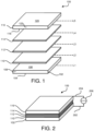
- FIG. 1 A simplified schematic of a multi-layer display device 100 with an electrochromic material is shown in FIG. 1 , in accordance with one or more implementations. For clarity purposes only, the various layers of the display device 100 in FIG. 1 are shown spaced apart (e.g., prior to lamination).
- the display device 100 includes a first layer "L1", a second layer “L2", a third layer “L3”, a fourth layer “L4', a fifth layer “L5", and possibly other layers.
- the second layer L2, the third layer L3, the fourth layer L4 are interposed (e.g., sandwiched) between the first layer L1 and the fifth layer L5.
- the first layer L1 comprises a first substrate 102 and possibly other components.
- the first substrate 102 depicts a display pattern (not shown in FIG. 1 ) formed by a conductive film coating and the display pattern may be formed on the first substrate 102 via photolithography and/or other patterning techniques.
- the first substrate 102 includes a first surface 104, a second surface 106 opposite the first surface 104, peripheral side edge 108 communicating between the first surface 104 and the second surface 106, a first conductive film coating (not shown ) on the second surface 106 and possibly other surfaces, and possibly other components.
- the display pattern is formed on the second surface 106 of the first substrate 102.
- the first conductive film coating may include indium tin oxide (ITO) and/or other materials. The thickness of the first substrate 102 may be dictated by the peripheral side edge 108.
- the fifth layer L5 comprises a second substrate 116 and possibly other components.
- the second substrate 116 may be devoid of depictions of patterns (e.g., a "non-patterned" substrate).
- the second substrate 116 includes a third surface 118, a fourth surface 120 opposite the third surface 118, peripheral side edge 122 communicating between the third surface 118 and the fourth surface 120, a second conductive film coating (not shown ) on the third surface, and possibly other components.
- the second conductive film coating may include indium tin oxide (ITO) and/or other materials.
- the second layer L2 comprises an electrochromic polymer 110 and possibly other components.
- the electrochromic polymer 110 may include a conductive polymer such as one or more of poly-3,4-ethylenedioxy thiophene (PEDOT), poly-2,2'-bithiophene, polypyrrole, polyaniline (PANI), polythiopene, polyisothianaphthene, poly(o-aminophenol), polypyridine, polyindole, polycarbazole, polyquinone, octacyanophthalocyanine, combinations thereof, and/or other polymer.
- PEDOT poly-3,4-ethylenedioxy thiophene
- PANI polyaniline
- PANI polyaniline
- polythiopene polyisothianaphthene
- poly(o-aminophenol) polypyridine
- polyindole polycarbazole
- polyquinone octacyanophthalocyanine
- combinations thereof and/or other polymer.
- the electrochromic polymer 110 may include other material such as one or more of as viologen, anthraquinone, phenocyazine, combinations thereof, and/or other material. In some implementations, the electrochromic polymer 110 may include a multicolored electrochromic polymer.
- the electrochromic polymer 110 is deposited on the second surface 106 of the first substrate 102.
- the electrochromic polymer 110 may be deposited via a wet coating process and/or other techniques.
- the wet coating process may include one or more of spin-coating, spray-coating, slot-die coating, dip-coating, blade-coating, meyer bar-coating, gravure-coating, ink-jet printing, screen printing, and/or other technique.
- the thickness of the electrochromic polymer 110 may depend on an extinction coefficient of the polymer.
- the third layer L3 comprises a solid state electrolyte 112 and possibly other components.
- the solid state electrolyte 112 may include one or more of Ta 2 O 5 , MgF, Li 3 N, LiPO 4 , LiBO 2 -Li 2 SO 4 , and/or other solid state electrolyte.
- the solid state electrolyte 112 may be deposited on either the electrochromic polymer 110 (prior to or after the electrochromic polymer 110 is deposited on the second surface 106) or the charge storage layer 114 (prior to or after the charge storage layer 114 is deposited on the third surface 118).
- a polymer based electrolyte may comprise one or more of an electrolyte salt (e.g., LiTFSI, LiPF 6 , LiBF 4 , LiClO 4 , LiCF 3 SO 3 , LiN(CF 3 SO 2 ) 2 , LiSbFg, LiAsF 6 , LiN(CF 3 CF 2 SO 2 ) 2 , (C 2 H 5 ) 4 NBF 4 , (C 2 H 5 ) 3 CH 3 NBF 4 , LiI, etc.), a polymer matrix (e.g., polyethylene oxide, poly(vinylidene fluoride( PVDF), poly(methyl methacrylate) (PMMA), polyethylene oxide (PEO), poly(acrylonitrile) (PAN), polyvinyl nitrile, etc.), one or more optional plasticizers (e.g., glutaronitrile, succinonitrile, adiponitrile, fumaronitrile, etc.), and/or other components.
- the fourth layer L4 comprises a charge storage layer 114 and possibly other components.
- the charge storage layer 114 is deposited on the third surface 118 of the second substrate 116.
- the charge storage layer 114 may include one or more of vanadium oxide, binary oxides (e.g., CoO, IrO 2 , MnO, NiO, and PrO x ), ternary oxides (e.g., Ce x V y O z ), and/or other materials.
- the charge storage layer 114 may be deposited on the third surface 118 via a wet coating process and/or other techniques.
- the first substrate 102 of the first layer and the second substrate 116 of the fifth layer are laminated together to form the multi-layer display device 100.
- the first substrate 102 and the second substrate 116 are laminated together with the second surface 106 of the first substrate 102 facing toward the third surface 118 of the second substrate 116.
- the first substrate 102 and the second substrate 116 may each have about an equal width, length, and/or thickness as one another; however, this need not be the case in other implementations.
- the first substrate 102, the electrochromic polymer 110, the solid state electrolyte 112, the charge storage layer 114, and/or the second substrate 116 may each have about an equal width, length, and/or thickness as one another; however, this need not be the case in other implementations.
- one or more of the electrochromic polymer 110, the solid state electrolyte 112, and/or the charge storage layer 114 may comprise films with minimal to no appreciably thickness.
- the thickness may vary between 10 ⁇ m and 100 ⁇ m.
- the size of the substrates may be larger than, smaller than, or of comparable thickness as other layers.
- the display device 100 may include one or more electrical leads coupled to the first conductive film coating of the first substrate 102 and/or the second conductive film coating of the second substrate 116.
- a first electrical lead 202 may be coupled to the first conductive film coating of the first substrate 102 and/or a second electrical lead 204 may be coupled the second conductive film coating of the second substrate 116.
- An application of a voltage 206 between the first substrate and the second substrate causes a change in transmission and/or reflectance of light through the display device 100 such that the display pattern on the first substrate 102 is displayed in a transparent state.
- An application of a reversed voltage between the first substrate and the second substrate causes a change in transmission and/or reflectance of light through the display device 100 such that the display pattern on the first substrate 102 is hidden.
- the first substrate 102 and/or second substrate 116 may comprise a rigid (non-pliant) material; a semi-rigid (semi-pliant) material; a pliant/flexible material, and/or combinations thereof.
- the first substrate 102 and/or second substrate 116 may comprise a transparent material.
- the first substrate 102 and/or second substrate 116 may be one or more of a transparent glass substrate, plastic substrate (e.g., PVC, EVA, PET, and/or other plastic), and/or other material.
- surfaces of the first substrate 102 and/or second substrate 116 to which the material may be deposited may be substantially flat, comprise one or more curved portions, and/or have any desired configuration/shape/dimensions as would be appreciated by skilled artisans upon reading the present disclosure.
- the corresponding dimensions e.g., width, height, etc.
- the corresponding dimensions may be about equal to one another and/or have other shapes.
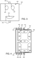
- FIG. 3 illustrates a substrate 300 depicting a display pattern 302, in accordance with one or more implementations.
- the substrate 300 includes a conductive film coating 304, 305, and/or 307 forming the display pattern 302.
- the display pattern 302 may be formed on the substrate 300 through photolithography and/or other techniques.
- the display pattern 302 forms an image.
- the image formed by display pattern 302 may comprise a smiley face.
- the substrate 300 may further include one or more electrical leads (e.g., first lead 306 and/or second lead 308) coupled to the conductive film coating 304, 305, and/or 307 forming the display pattern 302.
- FIG. 4 illustrates a substrate 400 depicting a display pattern 402, in accordance with one or more implementations.
- the display pattern 402 is formed of one or more segments of conductive film coating.
- the one or more segments may include one or more of a first segment 404, a second segment 406, a third segment 408, a fourth segment 410, a fifth segment 412, a sixth segment 414, a seventh segment 416, and/or other segments.
- electrochromic polymers may be deposited on top of the segments. Since the polymers may only needed on the conductive film coating segments, selective deposition of the electrochromic polymers may be performed.
- the selective deposition may include one or more of ink-jet printing, screen printing, and/or other techniques.
- blanket printing techniques may be used.
- the blanket printing techniques may include one or more of spin-coating, spray-coating, slot-die coating, dip-coating, blade-coating, meyer bar-coating, gravure-coating, and/or other techniques.
- the display pattern 402 may form an image wherein individual segments may be individually controlled.
- the image formed by display pattern 402 may comprise a pattern where display of individual segments and/or sets of segments may reproduce numbers between "0" and "9.”
- the substrate 400 may further include individual electrical leads coupled to individual ones of the segments to facilitate control of individual segments.
- a first set of leads 418 may be coupled to the first segment 404
- a second set of leads 420 may be coupled to the second segment 406
- a third set of leads 422 may be coupled to the third segment 408
- a fourth set of leads 424 may be coupled to the fourth segment 410
- a fifth set of leads 426 may be coupled to the fifth segment 412
- a sixth set of leads 428 may be coupled to the sixth segment 414
- a seventh set of leads 430 may be coupled to the seventh segment 416
- leads may be coupled to the segments and/or other segments.
- the display device may be connected to a display driver/controller by a cable (not shown).
- the display driver may control each segment individually.
- the driver may apply a positive and/or a negative (e.g., reversed) voltage to individual segments to alter the optical state of the polymer on the individual segments. By doing that, a number may be shown on the display device.
- the display pattern in said example not according to the present invention described with respect to FIG. 4 is considered as a "positive" image, like a photo.
- the display device When no image is shown, the display device is in a transparent state.
- the segments of the display pattern are turned to non-transparent state.
- Another variation of the display device, according to an embodiment of the present invention is to make "negative" image, like the developed film.
- the display device When no image is shown, the display device is in a non-transparent state.
- the segments are turned to a transparent state.
- the electrochromic polymer is blanket-deposited on the patterned substrate, possibly through wet coating process. There is no need to selectively deposit the polymer on top of the conducted film coated segment. The rest process is the same as that in making a positive image display as described herein an further with respect to FIG. 5 .
- FIG. 5 illustrates a flowchart of a method 500 to form a multi-layer display device including electrochromic materials, in accordance with one or more implementations.
- the method 500 may be implemented to construct one or more implementations of a display device described herein, such as those described with reference to FIG. 1-4 .
- the method 500 may be carried out in any desired environment, and may include more or less steps than those described and/or illustrated in FIG. 5 .
- the method 500 includes an operation 502 of providing a first substrate depicting a display pattern.
- the first substrate forms a layer of the display device.
- the first substrate includes a first surface, a second surface opposite the first surface, a first conductive film coating on the second surface, and possibly other components.
- the method 500 may include an operation (not shown) of forming the display pattern on the second surface of the first substrate via photolithography and/or other techniques.
- an electrochromic polymer is deposited on the first substrate.
- the electrochromic polymer forms a layer of the display device.
- Depositing the electrochromic polymer on the first substrate comprises depositing the electrochromic polymer on the second surface of the first substrate.
- a second substrate is provided.
- the second substrate forms a layer of the display device.
- the second substrate includes a third surface, a fourth surface opposite the third surface, a second conductive film covering on the third surface, and possibly other components.
- a charge storage layer is deposited on the second substrate.
- the charge storage layer forms a layer of the display device.
- Depositing the charge storage layer on the second substrate comprises depositing the charge storage layer on the third surface of the second substrate.
- a solid state electrolyte is interposed (e.g., sandwiched) between the first substrate and the second substrate.
- the solid state electrolyte forms a layer of the display device.
- the solid state electrolyte is deposited on either the electrochromic polymer or the charge storage layer.
- the first substrate and the second substrate are laminated together.
- Laminating the first substrate and the second substrate together comprises laminating the first substrate to the second substrate with the second surface of the first substrate facing toward the third surface of the second substrate.
- method 500 may include one or more other operations.
- the one or more other operations may include one or more of coupling one or more electrical leads to the first conductive film coating and/or the second conductive film coating.
- the method according to an embodiment of the present invention further comprises applying a voltage between the first substrate and the second substrate to cause a change in transmission and/or reflectance of light through the display device such that the display pattern on the first substrate is displayed in a transparent state; and applying a reversed voltage to cause the display pattern to to return to a non-transparent state so that no image is shown.
- the first substrate and/or the second substrate may comprise a transparent material.
- the first substrate and/or the second substrate may be transparent glass.
- the first substrate and/or the second substrate may comprise a rigid (non-pliant) material; a semi-rigid (semi-pliant) material; a pliant/flexible material; and/or combinations thereof.
- Implementations of the methods and systems disclosed herein may be used in various applications, devices, industries etc. For instance, several exemplary methods for integrating one or more electrochromic films onto and/or within a substrate structure have been presented herein. Such methods allow for a low cost, reproducible, and convenient process by which an end user may integrate the electrochromic film(s) with a display device.
Landscapes
- Physics & Mathematics (AREA)
- Nonlinear Science (AREA)
- General Physics & Mathematics (AREA)
- Optics & Photonics (AREA)
- Chemical & Material Sciences (AREA)
- Chemical Kinetics & Catalysis (AREA)
- Electrochemistry (AREA)
- Inorganic Chemistry (AREA)
- Electrochromic Elements, Electrophoresis, Or Variable Reflection Or Absorption Elements (AREA)
Description
- The invention generally relates to display devices utilizing electrochromic material.
- Electrochromism generally refers to a reversible change in optical properties of a material upon application of a potential. In particular, electrochromic materials could change the transmittance, reflectance, absorptance, and/or emittance under the applied voltage.
- Electrochromic materials are useful for a variety of applications, including photovoltaic devices, field effect transistors, organic light emitting diodes, general printed electronics, anti-glare window and display systems, etc.
-
US2002/0141033A1 discloses an apparatus and method of creating electrically modifiable images using a computer printer. One or more ink reservoirs of a printer cartridge are filled with electrochromic ink and electrochromic patterns can be printed on a surface using standard ink application methods. -
JPS6070419A - The invention provides a multi-layer display device including electrochromic material and a method to form a multi-layer display device including electrochromic materials as set out in the accompanying claims.
- An electrolyte is necessary in electrochromic device to provide mobile ions to dope and/or dedope the electrochromic material. Generally, the electrolyte exists in the form of a liquid. Conventionally, the liquid form possesses many disadvantages in actual applications. For example, it's difficult to assemble the device with liquid inside without leaking. Accordingly, it may be advantageous to use a solid polymer electrolyte. The solid polymer electrolyte could be dissolved in certain solvents and solution-deposited onto the substrate at room temperature. After the evaporation of the solvent, the polymer electrolyte becomes solid. The solid polymer electrolyte is distinguishable from aforementioned conventional liquid electrolytes, as well as gel polymer electrolytes including an ionic liquid therein in terms of the following advantages. The solid polymer electrolyte (i) has sufficient mechanical strength yet is versatile in shape so as to allow easy formation into thin films, and thin-film shaped products; (ii) avoids issues related to adhesion and print processing affecting conventional electrolytes; (iii) provides stable contact between the electrolyte/electrode interfaces (those with and without the electrochromic material coating thereon); (iv) avoids the problem of leakage commonly associated with liquid electrolytes; (v) has desirable non-toxic and non-flammable properties; (vi) avoids problems associated with evaporation due to its lack of vapor pressure; (vii) exhibits improved ion conductivities as compared to convention polymer electrolytes, which leads to faster switching time of the electrochromic device. Examples of solid state electrolyte in use with electrochromic devices are shown in
U.S. Patent Application No. US 15/487,325 filed on April 13, 2017 US 15/729,115 filed October 10, 2017 - Preferred and non-limiting implementations of the invention may be more readily understood by referring to the accompanying drawings in which:
-
FIG. 1 illustrates a schematic of a multi-layer display device, in accordance with one or more implementations -
FIG. 2 is a simplified schematic of a multi-layer display device laminated together, in accordance with one or more implementations -
FIG. 3 illustrates a substrate depicting a display pattern, in accordance with one or more implementations. -
FIG. 4 illustrates a substrate depicting a display pattern, in accordance with one or more implementations. -
FIG. 5 is a flowchart of a method to form a multi-layer display device including electrochromic materials, in accordance with one or more implementations. - In the following description, certain specific details are set forth in order to provide a thorough understanding of various implementations of the invention. However, one skilled in the art will understand that the invention may be practiced without these details. Moreover, while various implementations of the invention are disclosed herein, many adaptations and modifications may be made within the scope of the invention in accordance with the common general knowledge of those skilled in this art. Such
- Unless the context requires otherwise, throughout the present specification and claims, the word "comprise" and variations thereof, such as, "comprises" and "comprising" are to be construed in an open, inclusive sense, that is as "including, but not limited to." Recitation of numeric ranges of values throughout the specification is intended to serve as a shorthand notation of referring individually to each separate value falling within the range inclusive of the values defining the range, and each separate value is incorporated in the specification as it were individually recited herein. Additionally, the singular forms "a," "an" and "the" include plural referents unless the context clearly dictates otherwise.
- Reference throughout this specification to "some implementation" or "an implementation" means that a particular feature, structure, or characteristic described in connection with the implementation is included in at least one implementation of the present invention. Thus, the appearances of the phrases "in an implementation" or "in some implementations" in various places throughout this specification are not necessarily all referring to the same implementation, but may be in some instances. Furthermore, the particular features, structures, or characteristics may be combined in any suitable manner in one or more implementations.
- A simplified schematic of a
multi-layer display device 100 with an electrochromic material is shown inFIG. 1 , in accordance with one or more implementations. For clarity purposes only, the various layers of thedisplay device 100 inFIG. 1 are shown spaced apart (e.g., prior to lamination). - As shown in
FIG. 1 , thedisplay device 100 includes a first layer "L1", a second layer "L2", a third layer "L3", a fourth layer "L4', a fifth layer "L5", and possibly other layers. The second layer L2, the third layer L3, the fourth layer L4 are interposed (e.g., sandwiched) between the first layer L1 and the fifth layer L5. - The first layer L1 comprises a
first substrate 102 and possibly other components.
Thefirst substrate 102 depicts a display pattern (not shown inFIG. 1 ) formed by a conductive film coating and the display pattern may be formed on thefirst substrate 102 via photolithography and/or other patterning techniques. Thefirst substrate 102 includes afirst surface 104, asecond surface 106 opposite thefirst surface 104,peripheral side edge 108 communicating between thefirst surface 104 and thesecond surface 106, a first conductive film coating (not shown ) on thesecond surface 106 and possibly other surfaces, and possibly other components. The display pattern is formed on thesecond surface 106 of thefirst substrate 102. The first conductive film coating may include indium tin oxide (ITO) and/or other materials. The thickness of thefirst substrate 102 may be dictated by theperipheral side edge 108. - The fifth layer L5 comprises a
second substrate 116 and possibly other components. Thesecond substrate 116 may be devoid of depictions of patterns (e.g., a "non-patterned" substrate). Thesecond substrate 116 includes athird surface 118, afourth surface 120 opposite thethird surface 118,peripheral side edge 122 communicating between thethird surface 118 and thefourth surface 120, a second conductive film coating (not shown ) on the third surface, and possibly other components.
The second conductive film coating may include indium tin oxide (ITO) and/or other materials. - The second layer L2 comprises an
electrochromic polymer 110 and possibly other components. Theelectrochromic polymer 110 may include a conductive polymer such as one or more of poly-3,4-ethylenedioxy thiophene (PEDOT), poly-2,2'-bithiophene, polypyrrole, polyaniline (PANI), polythiopene, polyisothianaphthene, poly(o-aminophenol), polypyridine, polyindole, polycarbazole, polyquinone, octacyanophthalocyanine, combinations thereof, and/or other polymer. In some implementations, theelectrochromic polymer 110 may include other material such as one or more of as viologen, anthraquinone, phenocyazine, combinations thereof, and/or other material. In some implementations, theelectrochromic polymer 110 may include a multicolored electrochromic polymer. - The
electrochromic polymer 110 is deposited on thesecond surface 106 of thefirst substrate 102. Theelectrochromic polymer 110 may be deposited via a wet coating process and/or other techniques. The wet coating process may include one or more of spin-coating, spray-coating, slot-die coating, dip-coating, blade-coating, meyer bar-coating, gravure-coating, ink-jet printing, screen printing, and/or other technique. The thickness of theelectrochromic polymer 110 may depend on an extinction coefficient of the polymer. - The third layer L3 comprises a
solid state electrolyte 112 and possibly other components. Thesolid state electrolyte 112 may include one or more of Ta2O5, MgF, Li3N, LiPO4, LiBO2-Li2SO4, and/or other solid state electrolyte. Thesolid state electrolyte 112 may be deposited on either the electrochromic polymer 110 (prior to or after theelectrochromic polymer 110 is deposited on the second surface 106) or the charge storage layer 114 (prior to or after thecharge storage layer 114 is deposited on the third surface 118). - In some implementations, a polymer based electrolyte may comprise one or more of an electrolyte salt (e.g., LiTFSI, LiPF6, LiBF4, LiClO4, LiCF3SO3, LiN(CF3SO2)2, LiSbFg, LiAsF6, LiN(CF3CF2SO2)2, (C2H5)4NBF4, (C2H5)3CH3NBF4, LiI, etc.), a polymer matrix (e.g., polyethylene oxide, poly(vinylidene fluoride( PVDF), poly(methyl methacrylate) (PMMA), polyethylene oxide (PEO), poly(acrylonitrile) (PAN), polyvinyl nitrile, etc.), one or more optional plasticizers (e.g., glutaronitrile, succinonitrile, adiponitrile, fumaronitrile, etc.), and/or other components.
- The fourth layer L4 comprises a
charge storage layer 114 and possibly other components. Thecharge storage layer 114 is deposited on thethird surface 118 of thesecond substrate 116. Thecharge storage layer 114 may include one or more of vanadium oxide, binary oxides (e.g., CoO, IrO2, MnO, NiO, and PrOx), ternary oxides (e.g., CexVyOz), and/or other materials. Thecharge storage layer 114 may be deposited on thethird surface 118 via a wet coating process and/or other techniques. - As shown in
FIG. 2 , thefirst substrate 102 of the first layer and thesecond substrate 116 of the fifth layer are laminated together to form themulti-layer display device 100. Thefirst substrate 102 and thesecond substrate 116 are laminated together with thesecond surface 106 of thefirst substrate 102 facing toward thethird surface 118 of thesecond substrate 116. - In some implementations, the
first substrate 102 and thesecond substrate 116 may each have about an equal width, length, and/or thickness as one another; however, this need not be the case in other implementations. In some implementations, thefirst substrate 102, theelectrochromic polymer 110, thesolid state electrolyte 112, thecharge storage layer 114, and/or thesecond substrate 116 may each have about an equal width, length, and/or thickness as one another; however, this need not be the case in other implementations. By way of non-limiting illustration, in some implementations one or more of theelectrochromic polymer 110, thesolid state electrolyte 112, and/or thecharge storage layer 114 may comprise films with minimal to no appreciably thickness. In some implementations, the thickness may vary between 10 µm and 100 µm. In some implementations, the size of the substrates may be larger than, smaller than, or of comparable thickness as other layers. - In some implementations, the
display device 100 may include one or more electrical leads coupled to the first conductive film coating of thefirst substrate 102 and/or the second conductive film coating of thesecond substrate 116. By way of non-limiting illustration, as shown inFIG. 2 , a firstelectrical lead 202 may be coupled to the first conductive film coating of thefirst substrate 102 and/or a secondelectrical lead 204 may be coupled the second conductive film coating of thesecond substrate 116. An application of avoltage 206 between the first substrate and the second substrate causes a change in transmission and/or reflectance of light through thedisplay device 100 such that the display pattern on thefirst substrate 102 is displayed in a transparent state. An application of a reversed voltage between the first substrate and the second substrate causes a change in transmission and/or reflectance of light through thedisplay device 100 such that the display pattern on thefirst substrate 102 is hidden. - In some implementations, the
first substrate 102 and/orsecond substrate 116 may comprise a rigid (non-pliant) material; a semi-rigid (semi-pliant) material; a pliant/flexible material, and/or combinations thereof. In some implementations, thefirst substrate 102 and/orsecond substrate 116 may comprise a transparent material. In some implementations, thefirst substrate 102 and/orsecond substrate 116 may be one or more of a transparent glass substrate, plastic substrate (e.g., PVC, EVA, PET, and/or other plastic), and/or other material. - In some implementations, surfaces of the
first substrate 102 and/orsecond substrate 116 to which the material may be deposited may be substantially flat, comprise one or more curved portions, and/or have any desired configuration/shape/dimensions as would be appreciated by skilled artisans upon reading the present disclosure. - In some implementations, the corresponding dimensions (e.g., width, height, etc.) of one or more of: the
first substrate 102, theelectrochromic polymer 110, thesolid state electrolyte 112, thecharge storage layer 114, thesecond substrate 116, may be about equal to one another and/or have other shapes. -
FIG. 3 illustrates asubstrate 300 depicting adisplay pattern 302, in accordance with one or more implementations. Thesubstrate 300 includes aconductive film coating display pattern 302. Thedisplay pattern 302 may be formed on thesubstrate 300 through photolithography and/or other techniques. Thedisplay pattern 302 forms an image. InFIG. 3 , for illustrative purposes, the image formed bydisplay pattern 302 may comprise a smiley face. Thesubstrate 300 may further include one or more electrical leads (e.g.,first lead 306 and/or second lead 308) coupled to theconductive film coating display pattern 302. -
FIG. 4 illustrates asubstrate 400 depicting adisplay pattern 402, in accordance with one or more implementations. Thedisplay pattern 402 is formed of one or more segments of conductive film coating. The one or more segments may include one or more of afirst segment 404, asecond segment 406, athird segment 408, afourth segment 410, afifth segment 412, asixth segment 414, aseventh segment 416, and/or other segments. In an example not according to the present invention, after the segments are patterned, electrochromic polymers may be deposited on top of the segments. Since the polymers may only needed on the conductive film coating segments, selective deposition of the electrochromic polymers may be performed. The selective deposition may include one or more of ink-jet printing, screen printing, and/or other techniques. In some implementations of said example not according to the present invention, with the assistance of a mask, blanket printing techniques may be used. The blanket printing techniques may include one or more of spin-coating, spray-coating, slot-die coating, dip-coating, blade-coating, meyer bar-coating, gravure-coating, and/or other techniques. - The
display pattern 402 may form an image wherein individual segments may be individually controlled. InFIG. 4 , for illustrative purposes, the image formed bydisplay pattern 402 may comprise a pattern where display of individual segments and/or sets of segments may reproduce numbers between "0" and "9." Thesubstrate 400 may further include individual electrical leads coupled to individual ones of the segments to facilitate control of individual segments. By way of non-limiting illustration, a first set ofleads 418 may be coupled to thefirst segment 404, a second set ofleads 420 may be coupled to thesecond segment 406, a third set ofleads 422 may be coupled to thethird segment 408, a fourth set ofleads 424 may be coupled to thefourth segment 410, a fifth set ofleads 426 may be coupled to thefifth segment 412, a sixth set ofleads 428 may be coupled to thesixth segment 414, a seventh set ofleads 430 may be coupled to theseventh segment 416, and/or leads may be coupled to the segments and/or other segments. - After the display device is completed utilizing the substrate of
FIG. 4 , the display device may be connected to a display driver/controller by a cable (not shown). The display driver may control each segment individually. Depending on the number to be shown on the display device, the driver may apply a positive and/or a negative (e.g., reversed) voltage to individual segments to alter the optical state of the polymer on the individual segments. By doing that, a number may be shown on the display device. - It is noted that the display pattern in said example not according to the present invention described with respect to
FIG. 4 is considered as a "positive" image, like a photo. When no image is shown, the display device is in a transparent state. When the display pattern is to be shown, the segments of the display pattern are turned to non-transparent state. Another variation of the display device, according to an embodiment of the present invention, is to make "negative" image, like the developed film. When no image is shown, the display device is in a non-transparent state. When display pattern is to be shown, the segments are turned to a transparent state. To make such display device according to an embodiment of the present invention, the electrochromic polymer is blanket-deposited on the patterned substrate, possibly through wet coating process. There is no need to selectively deposit the polymer on top of the conducted film coated segment. The rest process is the same as that in making a positive image display as described herein an further with respect toFIG. 5 . -
FIG. 5 illustrates a flowchart of amethod 500 to form a multi-layer display device including electrochromic materials, in accordance with one or more implementations. Themethod 500 may be implemented to construct one or more implementations of a display device described herein, such as those described with reference toFIG. 1-4 . Themethod 500 may be carried out in any desired environment, and may include more or less steps than those described and/or illustrated inFIG. 5 . - As shown in
FIG. 5 , themethod 500 includes anoperation 502 of providing a first substrate depicting a display pattern. The first substrate forms a layer of the display device. The first substrate includes a first surface, a second surface opposite the first surface, a first conductive film coating on the second surface, and possibly other components. Themethod 500 may include an operation (not shown) of forming the display pattern on the second surface of the first substrate via photolithography and/or other techniques. - At an
operation 504, an electrochromic polymer is deposited on the first substrate. The electrochromic polymer forms a layer of the display device.
Depositing the electrochromic polymer on the first substrate comprises depositing the electrochromic polymer on the second surface of the first substrate. - At an
operation 506, a second substrate is provided. The second substrate forms a layer of the display device. The second substrate includes a third surface, a fourth surface opposite the third surface, a second conductive film covering on the third surface, and possibly other components. - At an
operation 508, a charge storage layer is deposited on the second substrate. The charge storage layer forms a layer of the display device. Depositing the charge storage layer on the second substrate comprises depositing the charge storage layer on the third surface of the second substrate. - At an
operation 510, a solid state electrolyte is interposed (e.g., sandwiched) between the first substrate and the second substrate. The solid state electrolyte forms a layer of the display device. - At an
operation 512, the solid state electrolyte is deposited on either the electrochromic polymer or the charge storage layer. - At an
operation 514, the first substrate and the second substrate are laminated together. Laminating the first substrate and the second substrate together comprises laminating the first substrate to the second substrate with the second surface of the first substrate facing toward the third surface of the second substrate. - Although not specifically shown,
method 500 may include one or more other operations. The one or more other operations may include one or more of coupling one or more electrical leads to the first conductive film coating and/or the second conductive film coating. In any case, the method according to an embodiment of the present invention further comprises applying a voltage between the first substrate and the second substrate to cause a change in transmission and/or reflectance of light through the display device such that the display pattern on the first substrate is displayed in a transparent state; and applying a reversed voltage to cause the display pattern to to return to a non-transparent state so that no image is shown. - In some implementations, the first substrate and/or the second substrate may comprise a transparent material. In an implementation, the first substrate and/or the second substrate may be transparent glass.
- In some implementations, the first substrate and/or the second substrate may comprise a rigid (non-pliant) material; a semi-rigid (semi-pliant) material; a pliant/flexible material; and/or combinations thereof.
- Implementations of the methods and systems disclosed herein may be used in various applications, devices, industries etc. For instance, several exemplary methods for integrating one or more electrochromic films onto and/or within a substrate structure have been presented herein. Such methods allow for a low cost, reproducible, and convenient process by which an end user may integrate the electrochromic film(s) with a display device.
- The invention described and claimed herein is not to be limited in scope by the specific preferred implementations disclosed herein, as these implementations are intended as illustrations of several aspects of the invention. Indeed, various modifications of the invention in addition to those shown and described herein will become apparent to those skilled in the art from the foregoing description. Such modifications may possibly fall within the scope of the appended claims.
Claims (10)
- A multi-layer display device (100) including electrochromic material, the display device comprising:a first layer comprising a first substrate (102; 300; 400) depicting a display pattern, wherein the first substrate (102; 300; 400) includes:a first surface (104);a second surface (106) opposite the first surface (104); anda first conductive film coating (304, 305 ,307; 404, 406, 408, 410, 412, 414, 416) on the second surface (106), and wherein the first conductive film coating (304, 305, 307; 404, 406, 408, 410, 412, 414, 416) forms the display pattern (302; 402);a second layer comprising an electrochromic polymer (110) deposited on the second surface (106) of the first substrate, whereinthe second surface (106) of the first substrate includes a first part coated by the first conductive film coating (304, 305, 307; 404, 406, 408, 410, 412, 414, 416) and a second part that is not coated by the first conductive film coating, wherein the electrochromic polymer (110) is deposited onto the first and second parts of the second surface;a third layer comprising a solid state electrolyte (112);a fourth layer comprising a charge storage layer (114);a fifth layer comprising a second substrate (116);wherein the second layer, the third layer, and the fourth layer are interposed between the first layer and the fifth layer;the second substrate (116) includes a third surface (118), a fourth surface (120) opposite the third surface (118), and a second conductive film covering on the third surface (118);the charge storage layer (114) is deposited on the third surface (118) of the second substrate;the solid state electrolyte (112) is deposited on either the electrochromic polymer (110) or the charge storage layer (114);the first substrate (102; 300; 400) and the second substrate (116) are laminated together with the second surface (106) of the first substrate facing toward the third surface (118) of the second substrate; andwherein, an application of a voltage between the first substrate (102; 300; 400) and the second substrate (116) causes a change in transmission or reflectance of light through the display device (100) such that the display pattern on the first substrate (102; 300; 400) is displayed in a transparent state, said display pattern depicting an image, and, wherein, if a reversed voltage is applied, the display device returns to a non-transparent state and no image is shown.
- The device of claim 1, further including one or more electrical leads (202, 204; 306, 308; 418, 420, 422, 424, 426, 428, 430) coupled to the first conductive film coating (304, 305, 307; 404, 406, 408, 410, 412, 414, 416) and the second conductive film coating.
- The device of claim 1, wherein the display pattern is formed on the second surface (106) of the first substrate via photolithography.
- The device of any one of the preceding claims, wherein the second substrate (116) is devoid of depictions of patterns.
- The device of any one of the preceding claims, wherein the first substrate (102; 300; 400) and/or the second substrate (116) are rigid or flexible.
- A method to form a multi-layer display device (100) including electrochromic materials, the method comprising:providing a first substrate (102; 300; 400) depicting a display pattern, the first substrate (102; 300; 400) forming a first layer, wherein the first substrate (102; 300; 400) includes:a first surface (104);a second surface (106) opposite the first surface (104); anda first conductive film coating (304, 305 ,307; 404, 406, 408, 410, 412, 414, 416) on the second surface (106), and wherein the first conductive film coating (304, 305, 307; 404, 406, 408, 410, 412, 414, 416) forms the display pattern;depositing an electrochromic polymer (110) on the second surface (106) of the first substrate, wherein the second surface (106) includes a first part coated by the first conductive film coating (304, 305, 307; 404, 406, 408, 410, 412, 414, 416) and a second part that is not coated by the first conductive film coating (304, 305, 307; 404, 406, 408, 410, 412, 414, 416), and the electrochromic polymer (110) is deposited onto the first and second parts of the second surface, and the electrochromic polymer (110) forms a second layer;providing a second substrate (116) including a third surface (118), a fourth surface (120) opposite the third surface (118), and a second conductive film covering on the third surface (118), the second substrate (116) forming a third layer;depositing a charge storage layer (114) on the third surface (118) of second substrate (116), the charge storage layer (114) forming a fourth layer;interposing a solid state electrolyte (112) between the first substrate (102; 300; 400) and the second substrate (116), the solid state electrolyte (112) forming a fifth layer;depositing the solid state electrolyte (112) on either the electrochromic polymer (110) or the charge storage layer (114); andlaminating the first substrate (102; 300; 400) to the second substrate (116) with the second surface (106) of the first substrate facing toward the third surface (118) of the second substrate, wherein an application of a voltage between the first substrate (102; 300; 400) and the second substrate (116) causes a change in transmission or reflectance of light through the display device such thatthe display pattern on the first substrate (102; 300; 400) is displayed in a transparent state, said display pattern depicting an image, and, wherein, if a reversed voltage is applied, the display device returns to a non-transparent state and no image is shown.
- The method of claim 6, further comprising:
coupling one or more electrical leads (202, 204; 306, 308; 418, 420, 422, 424, 426, 428, 430) to the first conductive film coating (304, 305, 307; 404, 406, 408, 410, 412, 414, 416) and the second conductive film coating. - The method of claim 6, further comprising:
forming the display pattern on the second surface (106) of the first substrate via photolithography. - The method of claims 6 to 8, wherein the first substrate (102; 300; 400) and/or the second substrate (116) are rigid or flexible.
- The method of any one of claims 6 to 9, wherein the depositing an electrochromic polymer (110) comprises wet coating the electrochromic polymer (110) on an entirety of the second surface (106).
Applications Claiming Priority (1)
| Application Number | Priority Date | Filing Date | Title |
|---|---|---|---|
| US16/222,701 US10983408B2 (en) | 2018-12-17 | 2018-12-17 | Display device with electrochromic material |
Publications (2)
| Publication Number | Publication Date |
|---|---|
| EP3671337A1 EP3671337A1 (en) | 2020-06-24 |
| EP3671337B1 true EP3671337B1 (en) | 2024-03-27 |
Family
ID=68424708
Family Applications (1)
| Application Number | Title | Priority Date | Filing Date |
|---|---|---|---|
| EP19206359.2A Active EP3671337B1 (en) | 2018-12-17 | 2019-10-30 | Display device with electrochromic material |
Country Status (4)
| Country | Link |
|---|---|
| US (1) | US10983408B2 (en) |
| EP (1) | EP3671337B1 (en) |
| CN (1) | CN111338148A (en) |
| ES (1) | ES2977645T3 (en) |
Families Citing this family (1)
| Publication number | Priority date | Publication date | Assignee | Title |
|---|---|---|---|---|
| KR102227394B1 (en) | 2012-12-24 | 2021-03-11 | 프레제니우스 메디칼 케어 홀딩스 인코퍼레이티드 | Portable dialysis machine with improved reservoir heating system |
Citations (1)
| Publication number | Priority date | Publication date | Assignee | Title |
|---|---|---|---|---|
| JPS6070419A (en) * | 1983-09-28 | 1985-04-22 | Toshiba Corp | Production of electrocoloring display element |
Family Cites Families (9)
| Publication number | Priority date | Publication date | Assignee | Title |
|---|---|---|---|---|
| US6501587B1 (en) * | 2000-09-27 | 2002-12-31 | Board Of Regents, The University Of Texas System | Method of creating color-changing displays |
| KR20060053111A (en) * | 2004-11-11 | 2006-05-19 | 주식회사 엘지화학 | Electrochromic mirror or window with information display |
| TWI273131B (en) | 2005-12-29 | 2007-02-11 | Ind Tech Res Inst | Electrochromic film |
| WO2010003138A1 (en) * | 2008-07-03 | 2010-01-07 | Ajjer Llc | Novel electrochromic materials, devices and applications of the same |
| JP2010054597A (en) * | 2008-08-26 | 2010-03-11 | Riso Kagaku Corp | Display device |
| EP2730973A1 (en) * | 2012-11-09 | 2014-05-14 | Acreo Swedish ICT AB | Fixed image display device and method of manufacturing the same |
| KR101552230B1 (en) * | 2014-04-24 | 2015-09-11 | 주식회사 티지오테크 | Heating Glass Panel Comprising Patterned Portion |
| CN107850816A (en) * | 2015-07-10 | 2018-03-27 | 唯景公司 | Bird-Friendly Electrochromic Devices |
| EP3281710A1 (en) | 2016-08-10 | 2018-02-14 | voestalpine Stahl GmbH | Coil coating method and metal strip |
-
2018
- 2018-12-17 US US16/222,701 patent/US10983408B2/en active Active
-
2019
- 2019-10-30 ES ES19206359T patent/ES2977645T3/en active Active
- 2019-10-30 EP EP19206359.2A patent/EP3671337B1/en active Active
- 2019-11-28 CN CN201911189584.0A patent/CN111338148A/en active Pending
Patent Citations (1)
| Publication number | Priority date | Publication date | Assignee | Title |
|---|---|---|---|---|
| JPS6070419A (en) * | 1983-09-28 | 1985-04-22 | Toshiba Corp | Production of electrocoloring display element |
Also Published As
| Publication number | Publication date |
|---|---|
| US20200192172A1 (en) | 2020-06-18 |
| EP3671337A1 (en) | 2020-06-24 |
| ES2977645T3 (en) | 2024-08-28 |
| US10983408B2 (en) | 2021-04-20 |
| CN111338148A (en) | 2020-06-26 |
Similar Documents
| Publication | Publication Date | Title |
|---|---|---|
| US20240083809A1 (en) | Integration of electrochromic films on a substrate | |
| JP5589801B2 (en) | Electrochromic display device and manufacturing method thereof | |
| JP5139323B2 (en) | Electrochromic display element and manufacturing method thereof | |
| US7158277B2 (en) | Electrochemical device | |
| US11969970B2 (en) | Electrochromic films with edge protection | |
| JP2016105150A (en) | Electrochromic device and manufacturing method of the same | |
| JP2010224240A (en) | Electrochromic display element and manufacturing method thereof | |
| US12543503B2 (en) | Piezoelectric films including ionic liquids and methods of making piezoelectric films including ionic liquids | |
| CN108604035B (en) | Integration of electrochromic films on substrates | |
| EP3537211A1 (en) | Method for changing the optical state of an electrochromic device | |
| KR102589425B1 (en) | Piezo electrophoretic display | |
| US10983408B2 (en) | Display device with electrochromic material | |
| KR102091612B1 (en) | Electrochromic device with enhanced discoloration rate and method of fabricating the same | |
| JP6582607B2 (en) | Electrochromic device, method for manufacturing the same, and electrochromic light control glasses | |
| US20250189856A1 (en) | Electrochromic device for camouflage | |
| KR102022784B1 (en) | Electrochromic device and fabricating method of the same, and electrolyte of the same | |
| JP2009053497A (en) | Electrochromic display element and manufacturing method thereof | |
| EP4211512B1 (en) | Electrochromic device | |
| JP2023134942A (en) | Laminated structure, lens, method for manufacturing a layered structure, and method for manufacturing a curved layered structure | |
| US20250172847A1 (en) | Piezo-Electrophoretic Films and Displays, and Methods for Manufacturing the Same | |
| US20250258417A1 (en) | Piezo-Electrophoretic Films and Displays, and Methods for Manufacturing the Same |
Legal Events
| Date | Code | Title | Description |
|---|---|---|---|
| PUAI | Public reference made under article 153(3) epc to a published international application that has entered the european phase |
Free format text: ORIGINAL CODE: 0009012 |
|
| STAA | Information on the status of an ep patent application or granted ep patent |
Free format text: STATUS: REQUEST FOR EXAMINATION WAS MADE |
|
| 17P | Request for examination filed |
Effective date: 20191030 |
|
| AK | Designated contracting states |
Kind code of ref document: A1 Designated state(s): AL AT BE BG CH CY CZ DE DK EE ES FI FR GB GR HR HU IE IS IT LI LT LU LV MC MK MT NL NO PL PT RO RS SE SI SK SM TR |
|
| AX | Request for extension of the european patent |
Extension state: BA ME |
|
| STAA | Information on the status of an ep patent application or granted ep patent |
Free format text: STATUS: EXAMINATION IS IN PROGRESS |
|
| 17Q | First examination report despatched |
Effective date: 20211025 |
|
| GRAP | Despatch of communication of intention to grant a patent |
Free format text: ORIGINAL CODE: EPIDOSNIGR1 |
|
| STAA | Information on the status of an ep patent application or granted ep patent |
Free format text: STATUS: GRANT OF PATENT IS INTENDED |
|
| INTG | Intention to grant announced |
Effective date: 20231010 |
|
| GRAS | Grant fee paid |
Free format text: ORIGINAL CODE: EPIDOSNIGR3 |
|
| GRAA | (expected) grant |
Free format text: ORIGINAL CODE: 0009210 |
|
| STAA | Information on the status of an ep patent application or granted ep patent |
Free format text: STATUS: THE PATENT HAS BEEN GRANTED |
|
| AK | Designated contracting states |
Kind code of ref document: B1 Designated state(s): AL AT BE BG CH CY CZ DE DK EE ES FI FR GB GR HR HU IE IS IT LI LT LU LV MC MK MT NL NO PL PT RO RS SE SI SK SM TR |
|
| REG | Reference to a national code |
Ref country code: GB Ref legal event code: FG4D |
|
| REG | Reference to a national code |
Ref country code: CH Ref legal event code: EP |
|
| REG | Reference to a national code |
Ref country code: DE Ref legal event code: R096 Ref document number: 602019048928 Country of ref document: DE |
|
| REG | Reference to a national code |
Ref country code: IE Ref legal event code: FG4D |
|
| PG25 | Lapsed in a contracting state [announced via postgrant information from national office to epo] |
Ref country code: LT Free format text: LAPSE BECAUSE OF FAILURE TO SUBMIT A TRANSLATION OF THE DESCRIPTION OR TO PAY THE FEE WITHIN THE PRESCRIBED TIME-LIMIT Effective date: 20240327 |
|
| REG | Reference to a national code |
Ref country code: LT Ref legal event code: MG9D |
|
| PG25 | Lapsed in a contracting state [announced via postgrant information from national office to epo] |
Ref country code: GR Free format text: LAPSE BECAUSE OF FAILURE TO SUBMIT A TRANSLATION OF THE DESCRIPTION OR TO PAY THE FEE WITHIN THE PRESCRIBED TIME-LIMIT Effective date: 20240628 |
|
| PG25 | Lapsed in a contracting state [announced via postgrant information from national office to epo] |
Ref country code: HR Free format text: LAPSE BECAUSE OF FAILURE TO SUBMIT A TRANSLATION OF THE DESCRIPTION OR TO PAY THE FEE WITHIN THE PRESCRIBED TIME-LIMIT Effective date: 20240327 Ref country code: RS Free format text: LAPSE BECAUSE OF FAILURE TO SUBMIT A TRANSLATION OF THE DESCRIPTION OR TO PAY THE FEE WITHIN THE PRESCRIBED TIME-LIMIT Effective date: 20240627 |
|
| PG25 | Lapsed in a contracting state [announced via postgrant information from national office to epo] |
Ref country code: RS Free format text: LAPSE BECAUSE OF FAILURE TO SUBMIT A TRANSLATION OF THE DESCRIPTION OR TO PAY THE FEE WITHIN THE PRESCRIBED TIME-LIMIT Effective date: 20240627 Ref country code: NO Free format text: LAPSE BECAUSE OF FAILURE TO SUBMIT A TRANSLATION OF THE DESCRIPTION OR TO PAY THE FEE WITHIN THE PRESCRIBED TIME-LIMIT Effective date: 20240627 Ref country code: LT Free format text: LAPSE BECAUSE OF FAILURE TO SUBMIT A TRANSLATION OF THE DESCRIPTION OR TO PAY THE FEE WITHIN THE PRESCRIBED TIME-LIMIT Effective date: 20240327 Ref country code: HR Free format text: LAPSE BECAUSE OF FAILURE TO SUBMIT A TRANSLATION OF THE DESCRIPTION OR TO PAY THE FEE WITHIN THE PRESCRIBED TIME-LIMIT Effective date: 20240327 Ref country code: GR Free format text: LAPSE BECAUSE OF FAILURE TO SUBMIT A TRANSLATION OF THE DESCRIPTION OR TO PAY THE FEE WITHIN THE PRESCRIBED TIME-LIMIT Effective date: 20240628 Ref country code: FI Free format text: LAPSE BECAUSE OF FAILURE TO SUBMIT A TRANSLATION OF THE DESCRIPTION OR TO PAY THE FEE WITHIN THE PRESCRIBED TIME-LIMIT Effective date: 20240327 Ref country code: BG Free format text: LAPSE BECAUSE OF FAILURE TO SUBMIT A TRANSLATION OF THE DESCRIPTION OR TO PAY THE FEE WITHIN THE PRESCRIBED TIME-LIMIT Effective date: 20240327 |
|
| REG | Reference to a national code |
Ref country code: NL Ref legal event code: MP Effective date: 20240327 |
|
| REG | Reference to a national code |
Ref country code: ES Ref legal event code: FG2A Ref document number: 2977645 Country of ref document: ES Kind code of ref document: T3 Effective date: 20240828 |
|
| PG25 | Lapsed in a contracting state [announced via postgrant information from national office to epo] |
Ref country code: SE Free format text: LAPSE BECAUSE OF FAILURE TO SUBMIT A TRANSLATION OF THE DESCRIPTION OR TO PAY THE FEE WITHIN THE PRESCRIBED TIME-LIMIT Effective date: 20240327 Ref country code: LV Free format text: LAPSE BECAUSE OF FAILURE TO SUBMIT A TRANSLATION OF THE DESCRIPTION OR TO PAY THE FEE WITHIN THE PRESCRIBED TIME-LIMIT Effective date: 20240327 |
|
| PG25 | Lapsed in a contracting state [announced via postgrant information from national office to epo] |
Ref country code: NL Free format text: LAPSE BECAUSE OF FAILURE TO SUBMIT A TRANSLATION OF THE DESCRIPTION OR TO PAY THE FEE WITHIN THE PRESCRIBED TIME-LIMIT Effective date: 20240327 |
|
| REG | Reference to a national code |
Ref country code: AT Ref legal event code: MK05 Ref document number: 1670479 Country of ref document: AT Kind code of ref document: T Effective date: 20240327 |
|
| PG25 | Lapsed in a contracting state [announced via postgrant information from national office to epo] |
Ref country code: NL Free format text: LAPSE BECAUSE OF FAILURE TO SUBMIT A TRANSLATION OF THE DESCRIPTION OR TO PAY THE FEE WITHIN THE PRESCRIBED TIME-LIMIT Effective date: 20240327 |
|
| PG25 | Lapsed in a contracting state [announced via postgrant information from national office to epo] |
Ref country code: IS Free format text: LAPSE BECAUSE OF FAILURE TO SUBMIT A TRANSLATION OF THE DESCRIPTION OR TO PAY THE FEE WITHIN THE PRESCRIBED TIME-LIMIT Effective date: 20240727 |
|
| PG25 | Lapsed in a contracting state [announced via postgrant information from national office to epo] |
Ref country code: PT Free format text: LAPSE BECAUSE OF FAILURE TO SUBMIT A TRANSLATION OF THE DESCRIPTION OR TO PAY THE FEE WITHIN THE PRESCRIBED TIME-LIMIT Effective date: 20240729 Ref country code: SM Free format text: LAPSE BECAUSE OF FAILURE TO SUBMIT A TRANSLATION OF THE DESCRIPTION OR TO PAY THE FEE WITHIN THE PRESCRIBED TIME-LIMIT Effective date: 20240327 |
|
| PG25 | Lapsed in a contracting state [announced via postgrant information from national office to epo] |
Ref country code: EE Free format text: LAPSE BECAUSE OF FAILURE TO SUBMIT A TRANSLATION OF THE DESCRIPTION OR TO PAY THE FEE WITHIN THE PRESCRIBED TIME-LIMIT Effective date: 20240327 Ref country code: CZ Free format text: LAPSE BECAUSE OF FAILURE TO SUBMIT A TRANSLATION OF THE DESCRIPTION OR TO PAY THE FEE WITHIN THE PRESCRIBED TIME-LIMIT Effective date: 20240327 |
|
| PG25 | Lapsed in a contracting state [announced via postgrant information from national office to epo] |
Ref country code: AT Free format text: LAPSE BECAUSE OF FAILURE TO SUBMIT A TRANSLATION OF THE DESCRIPTION OR TO PAY THE FEE WITHIN THE PRESCRIBED TIME-LIMIT Effective date: 20240327 |
|
| PG25 | Lapsed in a contracting state [announced via postgrant information from national office to epo] |
Ref country code: PL Free format text: LAPSE BECAUSE OF FAILURE TO SUBMIT A TRANSLATION OF THE DESCRIPTION OR TO PAY THE FEE WITHIN THE PRESCRIBED TIME-LIMIT Effective date: 20240327 |
|
| PG25 | Lapsed in a contracting state [announced via postgrant information from national office to epo] |
Ref country code: SK Free format text: LAPSE BECAUSE OF FAILURE TO SUBMIT A TRANSLATION OF THE DESCRIPTION OR TO PAY THE FEE WITHIN THE PRESCRIBED TIME-LIMIT Effective date: 20240327 |
|
| PG25 | Lapsed in a contracting state [announced via postgrant information from national office to epo] |
Ref country code: SM Free format text: LAPSE BECAUSE OF FAILURE TO SUBMIT A TRANSLATION OF THE DESCRIPTION OR TO PAY THE FEE WITHIN THE PRESCRIBED TIME-LIMIT Effective date: 20240327 Ref country code: SK Free format text: LAPSE BECAUSE OF FAILURE TO SUBMIT A TRANSLATION OF THE DESCRIPTION OR TO PAY THE FEE WITHIN THE PRESCRIBED TIME-LIMIT Effective date: 20240327 Ref country code: RO Free format text: LAPSE BECAUSE OF FAILURE TO SUBMIT A TRANSLATION OF THE DESCRIPTION OR TO PAY THE FEE WITHIN THE PRESCRIBED TIME-LIMIT Effective date: 20240327 Ref country code: PT Free format text: LAPSE BECAUSE OF FAILURE TO SUBMIT A TRANSLATION OF THE DESCRIPTION OR TO PAY THE FEE WITHIN THE PRESCRIBED TIME-LIMIT Effective date: 20240729 Ref country code: PL Free format text: LAPSE BECAUSE OF FAILURE TO SUBMIT A TRANSLATION OF THE DESCRIPTION OR TO PAY THE FEE WITHIN THE PRESCRIBED TIME-LIMIT Effective date: 20240327 Ref country code: IS Free format text: LAPSE BECAUSE OF FAILURE TO SUBMIT A TRANSLATION OF THE DESCRIPTION OR TO PAY THE FEE WITHIN THE PRESCRIBED TIME-LIMIT Effective date: 20240727 Ref country code: EE Free format text: LAPSE BECAUSE OF FAILURE TO SUBMIT A TRANSLATION OF THE DESCRIPTION OR TO PAY THE FEE WITHIN THE PRESCRIBED TIME-LIMIT Effective date: 20240327 Ref country code: CZ Free format text: LAPSE BECAUSE OF FAILURE TO SUBMIT A TRANSLATION OF THE DESCRIPTION OR TO PAY THE FEE WITHIN THE PRESCRIBED TIME-LIMIT Effective date: 20240327 Ref country code: AT Free format text: LAPSE BECAUSE OF FAILURE TO SUBMIT A TRANSLATION OF THE DESCRIPTION OR TO PAY THE FEE WITHIN THE PRESCRIBED TIME-LIMIT Effective date: 20240327 |
|
| REG | Reference to a national code |
Ref country code: DE Ref legal event code: R097 Ref document number: 602019048928 Country of ref document: DE |
|
| PG25 | Lapsed in a contracting state [announced via postgrant information from national office to epo] |
Ref country code: DK Free format text: LAPSE BECAUSE OF FAILURE TO SUBMIT A TRANSLATION OF THE DESCRIPTION OR TO PAY THE FEE WITHIN THE PRESCRIBED TIME-LIMIT Effective date: 20240327 |
|
| PG25 | Lapsed in a contracting state [announced via postgrant information from national office to epo] |
Ref country code: DK Free format text: LAPSE BECAUSE OF FAILURE TO SUBMIT A TRANSLATION OF THE DESCRIPTION OR TO PAY THE FEE WITHIN THE PRESCRIBED TIME-LIMIT Effective date: 20240327 |
|
| PLBE | No opposition filed within time limit |
Free format text: ORIGINAL CODE: 0009261 |
|
| STAA | Information on the status of an ep patent application or granted ep patent |
Free format text: STATUS: NO OPPOSITION FILED WITHIN TIME LIMIT |
|
| 26N | No opposition filed |
Effective date: 20250103 |
|
| PG25 | Lapsed in a contracting state [announced via postgrant information from national office to epo] |
Ref country code: SI Free format text: LAPSE BECAUSE OF FAILURE TO SUBMIT A TRANSLATION OF THE DESCRIPTION OR TO PAY THE FEE WITHIN THE PRESCRIBED TIME-LIMIT Effective date: 20240327 |
|
| REG | Reference to a national code |
Ref country code: CH Ref legal event code: PL |
|
| PG25 | Lapsed in a contracting state [announced via postgrant information from national office to epo] |
Ref country code: MC Free format text: LAPSE BECAUSE OF FAILURE TO SUBMIT A TRANSLATION OF THE DESCRIPTION OR TO PAY THE FEE WITHIN THE PRESCRIBED TIME-LIMIT Effective date: 20240327 |
|
| PG25 | Lapsed in a contracting state [announced via postgrant information from national office to epo] |
Ref country code: LU Free format text: LAPSE BECAUSE OF NON-PAYMENT OF DUE FEES Effective date: 20241030 Ref country code: BE Free format text: LAPSE BECAUSE OF NON-PAYMENT OF DUE FEES Effective date: 20241031 |
|
| PG25 | Lapsed in a contracting state [announced via postgrant information from national office to epo] |
Ref country code: CH Free format text: LAPSE BECAUSE OF NON-PAYMENT OF DUE FEES Effective date: 20241031 |
|
| REG | Reference to a national code |
Ref country code: BE Ref legal event code: MM Effective date: 20241031 |
|
| PG25 | Lapsed in a contracting state [announced via postgrant information from national office to epo] |
Ref country code: IE Free format text: LAPSE BECAUSE OF NON-PAYMENT OF DUE FEES Effective date: 20241030 |
|
| PGFP | Annual fee paid to national office [announced via postgrant information from national office to epo] |
Ref country code: DE Payment date: 20251029 Year of fee payment: 7 |
|
| PGFP | Annual fee paid to national office [announced via postgrant information from national office to epo] |
Ref country code: GB Payment date: 20251027 Year of fee payment: 7 |
|
| PGFP | Annual fee paid to national office [announced via postgrant information from national office to epo] |
Ref country code: IT Payment date: 20251021 Year of fee payment: 7 |
|
| PGFP | Annual fee paid to national office [announced via postgrant information from national office to epo] |
Ref country code: FR Payment date: 20251027 Year of fee payment: 7 |
|
| PGFP | Annual fee paid to national office [announced via postgrant information from national office to epo] |
Ref country code: ES Payment date: 20251103 Year of fee payment: 7 |
|
| PG25 | Lapsed in a contracting state [announced via postgrant information from national office to epo] |
Ref country code: HU Free format text: LAPSE BECAUSE OF FAILURE TO SUBMIT A TRANSLATION OF THE DESCRIPTION OR TO PAY THE FEE WITHIN THE PRESCRIBED TIME-LIMIT; INVALID AB INITIO Effective date: 20191030 |
|
| PG25 | Lapsed in a contracting state [announced via postgrant information from national office to epo] |
Ref country code: CY Free format text: LAPSE BECAUSE OF FAILURE TO SUBMIT A TRANSLATION OF THE DESCRIPTION OR TO PAY THE FEE WITHIN THE PRESCRIBED TIME-LIMIT; INVALID AB INITIO Effective date: 20191030 |